WO2020026401A1 - Dispositif à semi-conducteur à large bande interdite et dispositif de conversion de puissance - Google Patents
Dispositif à semi-conducteur à large bande interdite et dispositif de conversion de puissance Download PDFInfo
- Publication number
- WO2020026401A1 WO2020026401A1 PCT/JP2018/028993 JP2018028993W WO2020026401A1 WO 2020026401 A1 WO2020026401 A1 WO 2020026401A1 JP 2018028993 W JP2018028993 W JP 2018028993W WO 2020026401 A1 WO2020026401 A1 WO 2020026401A1
- Authority
- WO
- WIPO (PCT)
- Prior art keywords
- region
- band gap
- wide band
- electrode
- semiconductor device
- Prior art date
Links
- 239000004065 semiconductor Substances 0.000 title claims abstract description 137
- 238000006243 chemical reaction Methods 0.000 title claims description 37
- 238000000605 extraction Methods 0.000 claims abstract description 124
- 239000012535 impurity Substances 0.000 claims abstract description 43
- 238000009825 accumulation Methods 0.000 claims abstract description 30
- 238000003860 storage Methods 0.000 claims description 62
- 239000002344 surface layer Substances 0.000 claims description 35
- HBMJWWWQQXIZIP-UHFFFAOYSA-N silicon carbide Chemical group [Si+]#[C-] HBMJWWWQQXIZIP-UHFFFAOYSA-N 0.000 claims description 21
- 229910010271 silicon carbide Inorganic materials 0.000 claims description 19
- 238000000926 separation method Methods 0.000 claims description 11
- 230000004888 barrier function Effects 0.000 claims description 4
- 238000005516 engineering process Methods 0.000 abstract description 13
- 230000010354 integration Effects 0.000 abstract description 3
- 239000011229 interlayer Substances 0.000 description 24
- 239000010410 layer Substances 0.000 description 14
- 230000000694 effects Effects 0.000 description 12
- 230000000630 rising effect Effects 0.000 description 12
- 230000007704 transition Effects 0.000 description 12
- 238000000034 method Methods 0.000 description 11
- 230000015572 biosynthetic process Effects 0.000 description 10
- 229910052751 metal Inorganic materials 0.000 description 10
- 239000002184 metal Substances 0.000 description 10
- 239000000463 material Substances 0.000 description 8
- 239000000969 carrier Substances 0.000 description 7
- 238000004519 manufacturing process Methods 0.000 description 7
- 229920002120 photoresistant polymer Polymers 0.000 description 6
- 238000010438 heat treatment Methods 0.000 description 5
- VYPSYNLAJGMNEJ-UHFFFAOYSA-N Silicium dioxide Chemical compound O=[Si]=O VYPSYNLAJGMNEJ-UHFFFAOYSA-N 0.000 description 4
- 229910052782 aluminium Inorganic materials 0.000 description 4
- 238000005229 chemical vapour deposition Methods 0.000 description 4
- 230000005684 electric field Effects 0.000 description 4
- 238000002513 implantation Methods 0.000 description 4
- 238000005468 ion implantation Methods 0.000 description 4
- XLOMVQKBTHCTTD-UHFFFAOYSA-N Zinc monoxide Chemical compound [Zn]=O XLOMVQKBTHCTTD-UHFFFAOYSA-N 0.000 description 3
- 230000006378 damage Effects 0.000 description 3
- 238000002347 injection Methods 0.000 description 3
- 239000007924 injection Substances 0.000 description 3
- 238000000059 patterning Methods 0.000 description 3
- 238000000206 photolithography Methods 0.000 description 3
- 229910021332 silicide Inorganic materials 0.000 description 3
- FVBUAEGBCNSCDD-UHFFFAOYSA-N silicide(4-) Chemical compound [Si-4] FVBUAEGBCNSCDD-UHFFFAOYSA-N 0.000 description 3
- 238000004544 sputter deposition Methods 0.000 description 3
- XKRFYHLGVUSROY-UHFFFAOYSA-N Argon Chemical compound [Ar] XKRFYHLGVUSROY-UHFFFAOYSA-N 0.000 description 2
- IJGRMHOSHXDMSA-UHFFFAOYSA-N Atomic nitrogen Chemical compound N#N IJGRMHOSHXDMSA-UHFFFAOYSA-N 0.000 description 2
- 238000000137 annealing Methods 0.000 description 2
- 238000010586 diagram Methods 0.000 description 2
- 150000002500 ions Chemical class 0.000 description 2
- 238000004518 low pressure chemical vapour deposition Methods 0.000 description 2
- 230000004048 modification Effects 0.000 description 2
- 238000012986 modification Methods 0.000 description 2
- 229910052757 nitrogen Inorganic materials 0.000 description 2
- 230000003071 parasitic effect Effects 0.000 description 2
- 230000000149 penetrating effect Effects 0.000 description 2
- 229910021420 polycrystalline silicon Inorganic materials 0.000 description 2
- 229910052814 silicon oxide Inorganic materials 0.000 description 2
- 229910052719 titanium Inorganic materials 0.000 description 2
- 238000001039 wet etching Methods 0.000 description 2
- 208000032368 Device malfunction Diseases 0.000 description 1
- JMASRVWKEDWRBT-UHFFFAOYSA-N Gallium nitride Chemical compound [Ga]#N JMASRVWKEDWRBT-UHFFFAOYSA-N 0.000 description 1
- BUGBHKTXTAQXES-UHFFFAOYSA-N Selenium Chemical compound [Se] BUGBHKTXTAQXES-UHFFFAOYSA-N 0.000 description 1
- XUIMIQQOPSSXEZ-UHFFFAOYSA-N Silicon Chemical compound [Si] XUIMIQQOPSSXEZ-UHFFFAOYSA-N 0.000 description 1
- 239000000654 additive Substances 0.000 description 1
- 229910045601 alloy Inorganic materials 0.000 description 1
- 239000000956 alloy Substances 0.000 description 1
- XAGFODPZIPBFFR-UHFFFAOYSA-N aluminium Chemical compound [Al] XAGFODPZIPBFFR-UHFFFAOYSA-N 0.000 description 1
- 229910052786 argon Inorganic materials 0.000 description 1
- 230000015556 catabolic process Effects 0.000 description 1
- 150000004770 chalcogenides Chemical class 0.000 description 1
- 239000012141 concentrate Substances 0.000 description 1
- 239000000470 constituent Substances 0.000 description 1
- 238000010411 cooking Methods 0.000 description 1
- 229910003460 diamond Inorganic materials 0.000 description 1
- 239000010432 diamond Substances 0.000 description 1
- 238000005530 etching Methods 0.000 description 1
- 230000005669 field effect Effects 0.000 description 1
- 239000007789 gas Substances 0.000 description 1
- 229910052737 gold Inorganic materials 0.000 description 1
- 230000012447 hatching Effects 0.000 description 1
- 230000006698 induction Effects 0.000 description 1
- 239000011261 inert gas Substances 0.000 description 1
- 229910052750 molybdenum Inorganic materials 0.000 description 1
- 229910052759 nickel Inorganic materials 0.000 description 1
- 150000004767 nitrides Chemical class 0.000 description 1
- 230000001590 oxidative effect Effects 0.000 description 1
- 238000010248 power generation Methods 0.000 description 1
- 230000009467 reduction Effects 0.000 description 1
- 229910052711 selenium Inorganic materials 0.000 description 1
- 239000011669 selenium Substances 0.000 description 1
- SBIBMFFZSBJNJF-UHFFFAOYSA-N selenium;zinc Chemical compound [Se]=[Zn] SBIBMFFZSBJNJF-UHFFFAOYSA-N 0.000 description 1
- 229910052710 silicon Inorganic materials 0.000 description 1
- 239000010703 silicon Substances 0.000 description 1
- 235000012239 silicon dioxide Nutrition 0.000 description 1
- 239000000377 silicon dioxide Substances 0.000 description 1
- 239000002356 single layer Substances 0.000 description 1
- 229910052720 vanadium Inorganic materials 0.000 description 1
- 238000007740 vapor deposition Methods 0.000 description 1
- 239000011787 zinc oxide Substances 0.000 description 1
Images


Classifications
-
- H—ELECTRICITY
- H01—ELECTRIC ELEMENTS
- H01L—SEMICONDUCTOR DEVICES NOT COVERED BY CLASS H10
- H01L29/00—Semiconductor devices specially adapted for rectifying, amplifying, oscillating or switching and having potential barriers; Capacitors or resistors having potential barriers, e.g. a PN-junction depletion layer or carrier concentration layer; Details of semiconductor bodies or of electrodes thereof ; Multistep manufacturing processes therefor
- H01L29/66—Types of semiconductor device ; Multistep manufacturing processes therefor
- H01L29/68—Types of semiconductor device ; Multistep manufacturing processes therefor controllable by only the electric current supplied, or only the electric potential applied, to an electrode which does not carry the current to be rectified, amplified or switched
- H01L29/70—Bipolar devices
- H01L29/72—Transistor-type devices, i.e. able to continuously respond to applied control signals
- H01L29/739—Transistor-type devices, i.e. able to continuously respond to applied control signals controlled by field-effect, e.g. bipolar static induction transistors [BSIT]
- H01L29/7393—Insulated gate bipolar mode transistors, i.e. IGBT; IGT; COMFET
- H01L29/7395—Vertical transistors, e.g. vertical IGBT
- H01L29/7396—Vertical transistors, e.g. vertical IGBT with a non planar surface, e.g. with a non planar gate or with a trench or recess or pillar in the surface of the emitter, base or collector region for improving current density or short circuiting the emitter and base regions
- H01L29/7397—Vertical transistors, e.g. vertical IGBT with a non planar surface, e.g. with a non planar gate or with a trench or recess or pillar in the surface of the emitter, base or collector region for improving current density or short circuiting the emitter and base regions and a gate structure lying on a slanted or vertical surface or formed in a groove, e.g. trench gate IGBT
-
- H—ELECTRICITY
- H01—ELECTRIC ELEMENTS
- H01L—SEMICONDUCTOR DEVICES NOT COVERED BY CLASS H10
- H01L29/00—Semiconductor devices specially adapted for rectifying, amplifying, oscillating or switching and having potential barriers; Capacitors or resistors having potential barriers, e.g. a PN-junction depletion layer or carrier concentration layer; Details of semiconductor bodies or of electrodes thereof ; Multistep manufacturing processes therefor
- H01L29/02—Semiconductor bodies ; Multistep manufacturing processes therefor
- H01L29/06—Semiconductor bodies ; Multistep manufacturing processes therefor characterised by their shape; characterised by the shapes, relative sizes, or dispositions of the semiconductor regions ; characterised by the concentration or distribution of impurities within semiconductor regions
- H01L29/0603—Semiconductor bodies ; Multistep manufacturing processes therefor characterised by their shape; characterised by the shapes, relative sizes, or dispositions of the semiconductor regions ; characterised by the concentration or distribution of impurities within semiconductor regions characterised by particular constructional design considerations, e.g. for preventing surface leakage, for controlling electric field concentration or for internal isolations regions
- H01L29/0607—Semiconductor bodies ; Multistep manufacturing processes therefor characterised by their shape; characterised by the shapes, relative sizes, or dispositions of the semiconductor regions ; characterised by the concentration or distribution of impurities within semiconductor regions characterised by particular constructional design considerations, e.g. for preventing surface leakage, for controlling electric field concentration or for internal isolations regions for preventing surface leakage or controlling electric field concentration
- H01L29/0611—Semiconductor bodies ; Multistep manufacturing processes therefor characterised by their shape; characterised by the shapes, relative sizes, or dispositions of the semiconductor regions ; characterised by the concentration or distribution of impurities within semiconductor regions characterised by particular constructional design considerations, e.g. for preventing surface leakage, for controlling electric field concentration or for internal isolations regions for preventing surface leakage or controlling electric field concentration for increasing or controlling the breakdown voltage of reverse biased devices
- H01L29/0615—Semiconductor bodies ; Multistep manufacturing processes therefor characterised by their shape; characterised by the shapes, relative sizes, or dispositions of the semiconductor regions ; characterised by the concentration or distribution of impurities within semiconductor regions characterised by particular constructional design considerations, e.g. for preventing surface leakage, for controlling electric field concentration or for internal isolations regions for preventing surface leakage or controlling electric field concentration for increasing or controlling the breakdown voltage of reverse biased devices by the doping profile or the shape or the arrangement of the PN junction, or with supplementary regions, e.g. junction termination extension [JTE]
- H01L29/0619—Semiconductor bodies ; Multistep manufacturing processes therefor characterised by their shape; characterised by the shapes, relative sizes, or dispositions of the semiconductor regions ; characterised by the concentration or distribution of impurities within semiconductor regions characterised by particular constructional design considerations, e.g. for preventing surface leakage, for controlling electric field concentration or for internal isolations regions for preventing surface leakage or controlling electric field concentration for increasing or controlling the breakdown voltage of reverse biased devices by the doping profile or the shape or the arrangement of the PN junction, or with supplementary regions, e.g. junction termination extension [JTE] with a supplementary region doped oppositely to or in rectifying contact with the semiconductor containing or contacting region, e.g. guard rings with PN or Schottky junction
-
- H—ELECTRICITY
- H01—ELECTRIC ELEMENTS
- H01L—SEMICONDUCTOR DEVICES NOT COVERED BY CLASS H10
- H01L29/00—Semiconductor devices specially adapted for rectifying, amplifying, oscillating or switching and having potential barriers; Capacitors or resistors having potential barriers, e.g. a PN-junction depletion layer or carrier concentration layer; Details of semiconductor bodies or of electrodes thereof ; Multistep manufacturing processes therefor
- H01L29/02—Semiconductor bodies ; Multistep manufacturing processes therefor
- H01L29/06—Semiconductor bodies ; Multistep manufacturing processes therefor characterised by their shape; characterised by the shapes, relative sizes, or dispositions of the semiconductor regions ; characterised by the concentration or distribution of impurities within semiconductor regions
- H01L29/0684—Semiconductor bodies ; Multistep manufacturing processes therefor characterised by their shape; characterised by the shapes, relative sizes, or dispositions of the semiconductor regions ; characterised by the concentration or distribution of impurities within semiconductor regions characterised by the shape, relative sizes or dispositions of the semiconductor regions or junctions between the regions
- H01L29/0692—Surface layout
- H01L29/0696—Surface layout of cellular field-effect devices, e.g. multicellular DMOS transistors or IGBTs
-
- H—ELECTRICITY
- H01—ELECTRIC ELEMENTS
- H01L—SEMICONDUCTOR DEVICES NOT COVERED BY CLASS H10
- H01L29/00—Semiconductor devices specially adapted for rectifying, amplifying, oscillating or switching and having potential barriers; Capacitors or resistors having potential barriers, e.g. a PN-junction depletion layer or carrier concentration layer; Details of semiconductor bodies or of electrodes thereof ; Multistep manufacturing processes therefor
- H01L29/02—Semiconductor bodies ; Multistep manufacturing processes therefor
- H01L29/12—Semiconductor bodies ; Multistep manufacturing processes therefor characterised by the materials of which they are formed
- H01L29/16—Semiconductor bodies ; Multistep manufacturing processes therefor characterised by the materials of which they are formed including, apart from doping materials or other impurities, only elements of Group IV of the Periodic Table
- H01L29/1608—Silicon carbide
-
- H—ELECTRICITY
- H01—ELECTRIC ELEMENTS
- H01L—SEMICONDUCTOR DEVICES NOT COVERED BY CLASS H10
- H01L29/00—Semiconductor devices specially adapted for rectifying, amplifying, oscillating or switching and having potential barriers; Capacitors or resistors having potential barriers, e.g. a PN-junction depletion layer or carrier concentration layer; Details of semiconductor bodies or of electrodes thereof ; Multistep manufacturing processes therefor
- H01L29/40—Electrodes ; Multistep manufacturing processes therefor
- H01L29/41—Electrodes ; Multistep manufacturing processes therefor characterised by their shape, relative sizes or dispositions
- H01L29/417—Electrodes ; Multistep manufacturing processes therefor characterised by their shape, relative sizes or dispositions carrying the current to be rectified, amplified or switched
-
- H—ELECTRICITY
- H01—ELECTRIC ELEMENTS
- H01L—SEMICONDUCTOR DEVICES NOT COVERED BY CLASS H10
- H01L29/00—Semiconductor devices specially adapted for rectifying, amplifying, oscillating or switching and having potential barriers; Capacitors or resistors having potential barriers, e.g. a PN-junction depletion layer or carrier concentration layer; Details of semiconductor bodies or of electrodes thereof ; Multistep manufacturing processes therefor
- H01L29/40—Electrodes ; Multistep manufacturing processes therefor
- H01L29/43—Electrodes ; Multistep manufacturing processes therefor characterised by the materials of which they are formed
- H01L29/47—Schottky barrier electrodes
-
- H—ELECTRICITY
- H01—ELECTRIC ELEMENTS
- H01L—SEMICONDUCTOR DEVICES NOT COVERED BY CLASS H10
- H01L29/00—Semiconductor devices specially adapted for rectifying, amplifying, oscillating or switching and having potential barriers; Capacitors or resistors having potential barriers, e.g. a PN-junction depletion layer or carrier concentration layer; Details of semiconductor bodies or of electrodes thereof ; Multistep manufacturing processes therefor
- H01L29/66—Types of semiconductor device ; Multistep manufacturing processes therefor
- H01L29/66007—Multistep manufacturing processes
- H01L29/66075—Multistep manufacturing processes of devices having semiconductor bodies comprising group 14 or group 13/15 materials
- H01L29/66227—Multistep manufacturing processes of devices having semiconductor bodies comprising group 14 or group 13/15 materials the devices being controllable only by the electric current supplied or the electric potential applied, to an electrode which does not carry the current to be rectified, amplified or switched, e.g. three-terminal devices
- H01L29/66234—Bipolar junction transistors [BJT]
- H01L29/66325—Bipolar junction transistors [BJT] controlled by field-effect, e.g. insulated gate bipolar transistors [IGBT]
- H01L29/66333—Vertical insulated gate bipolar transistors
-
- H—ELECTRICITY
- H01—ELECTRIC ELEMENTS
- H01L—SEMICONDUCTOR DEVICES NOT COVERED BY CLASS H10
- H01L29/00—Semiconductor devices specially adapted for rectifying, amplifying, oscillating or switching and having potential barriers; Capacitors or resistors having potential barriers, e.g. a PN-junction depletion layer or carrier concentration layer; Details of semiconductor bodies or of electrodes thereof ; Multistep manufacturing processes therefor
- H01L29/66—Types of semiconductor device ; Multistep manufacturing processes therefor
- H01L29/68—Types of semiconductor device ; Multistep manufacturing processes therefor controllable by only the electric current supplied, or only the electric potential applied, to an electrode which does not carry the current to be rectified, amplified or switched
- H01L29/70—Bipolar devices
- H01L29/72—Transistor-type devices, i.e. able to continuously respond to applied control signals
- H01L29/739—Transistor-type devices, i.e. able to continuously respond to applied control signals controlled by field-effect, e.g. bipolar static induction transistors [BSIT]
- H01L29/7393—Insulated gate bipolar mode transistors, i.e. IGBT; IGT; COMFET
- H01L29/7395—Vertical transistors, e.g. vertical IGBT
-
- H—ELECTRICITY
- H01—ELECTRIC ELEMENTS
- H01L—SEMICONDUCTOR DEVICES NOT COVERED BY CLASS H10
- H01L29/00—Semiconductor devices specially adapted for rectifying, amplifying, oscillating or switching and having potential barriers; Capacitors or resistors having potential barriers, e.g. a PN-junction depletion layer or carrier concentration layer; Details of semiconductor bodies or of electrodes thereof ; Multistep manufacturing processes therefor
- H01L29/66—Types of semiconductor device ; Multistep manufacturing processes therefor
- H01L29/68—Types of semiconductor device ; Multistep manufacturing processes therefor controllable by only the electric current supplied, or only the electric potential applied, to an electrode which does not carry the current to be rectified, amplified or switched
- H01L29/76—Unipolar devices, e.g. field effect transistors
- H01L29/772—Field effect transistors
- H01L29/78—Field effect transistors with field effect produced by an insulated gate
Definitions
- the technology disclosed in the present specification relates to a wide band gap semiconductor device and a power conversion device.
- MOSFETs metal-oxide-semiconductor field-effect transistors
- IGBTs Insulated gate bipolar transistors
- a voltage drop due to a hole current flowing in a P-type base region when shifting from an ON state in which a main current flows to an OFF state in which a main current does not flow is represented by N
- the built-in voltage between the emitter region having a relatively high concentration of impurity (N + ) and the base region of the P-type is exceeded, the parasitic thyristor is turned on, and furthermore, the latch-up state in which current continues to flow
- N + concentration of impurity
- Patent Document 1 in an IGBT having a trench gate, a dummy cell that allows a hole current to flow to an emitter electrode is formed in addition to a main cell that allows a main current to flow. Furthermore, a structure having a rectifying element connected in series is disclosed in the dummy cell.
- the built-in voltage of the rectifying element is about 0.7 V, which corresponds to the built-in potential of a PN junction of Si.
- the PN junction between the emitter region and the base region is formed of Si
- the PN junction has a built-in voltage of about 0.7 V as in the case of the rectifier.
- a voltage of 0.7 V is applied to the rectifying element to conduct the voltage
- a voltage of about 0.7 V may be applied to the PN junction between the emitter region and the base region to conduct the rectifying element.
- the IGBT and the rectifying element are made of a PN junction of SiC, and both have a built-in voltage of about 2.5 V, so that sufficient latch-up withstand capability cannot be obtained.
- the IGBT can be made of SiC and the rectifying element can be made of Si to make a difference in the built-in voltage.
- the IGBT and the rectifying element cannot be formed densely, the resistance value per unit area is reduced. It cannot be reduced.
- the rectifying element is provided outside the device. Therefore, an electrode (specifically, a diverter electrode) different from the gate electrode or the emitter electrode is required to connect the P-type region in the dummy cell and the rectifying element.
- the diverter electrode and the rectifying element are connected by, for example, a method such as wire bonding. For this reason, an electrode pad having a relatively large area (specifically, a diverter electrode pad) needs to be formed on the device, and integration has been difficult.
- the technology disclosed in the present specification has been made in order to solve the problems described above, and provides a technology that can obtain sufficient latch-up withstand capability and can be integrated. The purpose is to do so.
- a drift region including a wide band gap semiconductor of a first conductivity type, and a wide band gap of a second conductivity type formed on a lower surface of the drift region.
- a collector region made of a semiconductor, a charge accumulation region formed on a top surface of the drift region and having a higher impurity concentration than the drift region, made of a first conductivity type wide band gap semiconductor; and the charge accumulation region
- a base region of the second conductivity type which is formed partially on the surface layer of the charge storage region, and is formed apart from the base region on the surface layer of the charge storage region, and has a higher impurity concentration than the base region;
- a first conductivity type emitter region having a material concentration, a Schottky electrode formed in contact with the charge extraction region and Schottky-connected to the charge extraction region, the charge
- a conversion circuit that has the above-described wide band gap semiconductor device, and that converts input power and outputs the converted power.
- FIG. 1 is a cross-sectional view schematically showing an example of a configuration of an IGBT as a semiconductor device according to an embodiment.
- FIG. 3 is a plan view schematically showing an example of a configuration of a semiconductor device according to an embodiment when an upper electrode and a dielectric film formed after semiconductor element formation are omitted.
- FIG. 3 is a plan view schematically showing an example of a configuration of a semiconductor device according to an embodiment when unit cells are arranged in a comb shape.
- FIG. 11 is a plan view schematically showing an example of a configuration of a semiconductor device according to an embodiment when unit cells are arranged in a ladder shape.
- FIG. 1 is a cross-sectional view schematically showing an example of a configuration of an IGBT as a semiconductor device according to an embodiment.
- FIG. 3 is a plan view schematically showing an example of a configuration of a semiconductor device according to an embodiment when an upper electrode and a dielectric film formed after semiconductor element formation are omitted.
- FIG. 3
- FIG. 11 is a plan view schematically showing an example of a configuration of a semiconductor device according to an embodiment when unit cells are arranged in a stripe shape.
- FIG. 2 is a cross-sectional view schematically illustrating an example of a configuration of an IGBT according to the embodiment.
- FIG. 2 is a cross-sectional view schematically illustrating an example of a configuration of an IGBT according to the embodiment.
- FIG. 2 is a cross-sectional view schematically illustrating an example of a configuration of an IGBT according to the embodiment.
- FIG. 3 is a plan view schematically showing an example of a configuration of a semiconductor device according to an embodiment when an upper electrode and a dielectric film formed after semiconductor element formation are omitted.
- FIG. 3 is a plan view schematically showing an example of a configuration of a semiconductor device according to an embodiment when an upper electrode and a dielectric film formed after semiconductor element formation are omitted.
- FIG. 3 is a plan view schematically showing an example of a configuration of a semiconductor device according to an embodiment when an upper electrode and a dielectric film formed after semiconductor element formation are omitted.
- FIG. 2 is a cross-sectional view schematically illustrating an example of a configuration of an IGBT according to the embodiment.
- 1 is a diagram conceptually illustrating an example of a configuration of a power conversion system including a power conversion device according to an embodiment.
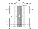
- FIG. 1 is a sectional view schematically showing an example of the configuration of an IGBT 100 as a semiconductor device according to the present embodiment.
- FIG. 2 is a plan view schematically showing an example of the configuration of the semiconductor device according to the present embodiment when the upper electrode and the dielectric film formed after the formation of the semiconductor element are omitted.
- FIG. 1 corresponds to a section taken along the line AA ′ in FIG.
- FIG. 2 illustrates an example in which the unit cells are arranged in a lattice shape.
- the arrangement of the unit cells may also be a case where the unit cells are arranged in a comb shape, a case where the unit cells are arranged in a ladder shape, or It is also assumed that they are arranged in stripes.
- FIG. 3 is a plan view schematically showing an example of the configuration of the semiconductor device according to the present embodiment when the unit cells are arranged in a comb shape.
- FIG. 4 is a plan view schematically showing an example of the configuration of the semiconductor device according to the present embodiment when the unit cells are arranged in a ladder shape.
- FIG. 5 is a plan view schematically showing an example of the configuration of the semiconductor device according to the present embodiment when the unit cells are arranged in a stripe shape.
- FIG. 1 corresponds to a cross section taken along line A-A ′ in each of FIGS. 3, 4, and 5.
- the IGBT 100 includes a P-type collector region 10 having a relatively high concentration (P + ) of P-type impurities and one main surface of the collector region 10 (that is, the upper surface). And an N-type charge accumulation region 21 laminated on the upper surface of the drift region 20.
- the charge accumulation region 21 has a higher impurity concentration than the drift region 20.
- the semiconductor material used for the IGBT 100 is a wide band gap semiconductor having a larger band gap than a silicon semiconductor, and may be, for example, silicon carbide.
- a wide band gap semiconductor generally refers to a semiconductor having a forbidden band width of about 2 eV or more, a group 3 nitride such as gallium nitride (GaN), a group 2 oxide such as zinc oxide (ZnO), and selenium.
- Group 2 chalcogenides such as zinc oxide (ZnSe), diamond, and silicon carbide (SiC) are known.
- SiC silicon carbide
- a planar gate type SiC-IGBT in which the channel region is formed perpendicular to the thickness direction of IGBT 100 (that is, the vertical direction in FIG. 1) will be described as an example.
- a plurality of base regions 30 made of a P-type wide band gap semiconductor are selectively provided.
- An emitter region 40 made of an N-type wide band gap semiconductor is formed on each surface layer of the base region 30 at a position inside the outer periphery of the base region 30 at a predetermined interval.
- the emitter region 40 has a higher impurity concentration than the charge storage region 21.
- a well contact region 31 made of a low-resistance P-type wide band gap semiconductor is formed inside each emitter region 40.
- Well contact region 31 is formed to reach base region 30 from the upper surface of emitter region 40.
- a charge extraction region 32 made of a P-type wide band gap semiconductor is formed so as to be separated from the base region 30.
- the charge extraction region 32 has a higher impurity concentration than the base region 30.
- An ohmic electrode 70 is formed over a part of the upper surface of the emitter region 40 and a part of the upper surface of the well contact region 31.
- the ohmic electrode 70 is in ohmic connection with the wide band gap semiconductor.
- Schottky electrode 71 is formed on the upper surface of the charge extraction region 32. Schottky electrode 71 is Schottky-connected to P-type silicon carbide semiconductor layer (charge extraction region 32).
- the rising voltage when a forward voltage is applied to the Schottky connection is set to be, for example, 0.2 V or more and 2.0 V or less.
- the rising voltage may be, for example, 1.0 V.
- the gate insulating film 50 is formed over the upper surface of the base region 30 and the upper surface of the charge extraction region 32. Gate insulating film 50 is formed in contact with base region 30 at a position sandwiched between charge storage region 21 and emitter region 40. Further, a gate electrode 60 is formed via a gate insulating film 50 at a position overlapping the base region 30 in plan view. Further, an interlayer insulating film 55 is formed to cover the gate electrode 60.
- the emitter electrode 80 is formed so as to cover the open upper surface of the ohmic electrode 70, the open upper surface of the Schottky electrode 71, and the upper surface of the interlayer insulating film 55.
- the emitter electrode 80 is electrically connected to the ohmic electrode 70 and the Schottky electrode 71.
- An interlayer insulating film 55 is formed between the emitter electrode 80 and the gate electrode 60.
- a collector electrode 81 is formed on the lower surface of the collector region 10.
- FIG. 2 is a plan view schematically showing an example of the configuration of the semiconductor device according to the present embodiment.
- the IGBT 100 has an emitter region 40 surrounding the well contact region 31. Further, a base region 30 is formed surrounding the emitter region 40. Further, a charge storage region 21 is formed surrounding the base region 30.
- Each cell region is two-dimensionally arranged in the horizontal direction and the vertical direction in FIG.
- a charge extraction region 32 is formed in a region where a cell region is not formed.
- the charge extraction region 32 is formed in a region extending in the left-right direction where no cell region is formed and a region extending in the vertical direction where no cell region is formed.
- FIG. 3 is a plan view schematically showing an example of the configuration of the semiconductor device according to the present embodiment when the unit cells are arranged in a comb shape.
- an emitter region 40A is formed with a well contact region 31A interposed therebetween.
- base region 30A is formed with emitter region 40A interposed therebetween.
- a charge accumulation region 21A is formed with the base region 30A interposed therebetween.
- the comb-shaped cell regions thus formed are formed apart from each other, and a charge extraction region 32A is formed in a region between the cell regions.
- FIG. 4 is a plan view schematically showing an example of the configuration of the semiconductor device according to the present embodiment when the unit cells are arranged in a ladder shape.
- the emitter region 40B is formed with the well contact region 31B formed intermittently in the longitudinal direction.
- base region 30B is formed with emitter region 40B interposed therebetween.
- the charge accumulation region 21B is formed with the base region 30B interposed therebetween.
- the ladder-shaped cell regions thus formed are formed apart from each other, and a charge extraction region 32B is formed in a region between the cell regions.
- FIG. 5 is a plan view schematically showing an example of a configuration of a semiconductor device according to the present embodiment when unit cells are arranged in a stripe shape.
- an emitter region 40C is formed with a well contact region 31C formed intermittently in the longitudinal direction.
- the base region 30C is formed in partial contact with the well contact region 31C while sandwiching the emitter region 40C.
- a charge storage region 21C is formed with the base region 30C interposed therebetween.
- the stripe-shaped cell regions thus formed are formed apart from each other, and a charge extraction region 32C is formed in a region between the cell regions.
- an impurity concentration is, for example, 5 ⁇ 10 13 cm ⁇ 3 or more and 1 ⁇ 10 15 cm ⁇ 3 or less, for example, on the upper surface of the collector region 10 by a chemical vapor deposition (CVD) method.
- CVD chemical vapor deposition
- a drift region 20 made of N-type silicon carbide having a thickness of, for example, 50 ⁇ m or more and 200 ⁇ m or less is epitaxially grown.
- collector region 10 is a (0001) plane in which the plane orientation of the first main surface has an off angle, and is made of P-type, low-resistance silicon carbide having a 4H polytype. .
- the charge accumulation region 21 having an impurity concentration of, for example, 1 ⁇ 10 15 cm ⁇ 3 or more and 1 ⁇ 10 17 cm ⁇ 3 or less, and a film thickness of, for example, 1 ⁇ m or more and 10 ⁇ m or less, Epitaxial growth is performed on the upper surface of the drift region 20.
- an injection mask is formed in a predetermined region on the upper surface of the charge accumulation region 21 by using a photoresist or the like. Then, Al (aluminum), which is a P-type impurity, is ion-implanted.
- the depth of the Al ion implantation is, for example, 0.5 ⁇ m or more and 3 ⁇ m or less.
- the impurity concentration of ion-implanted Al is, for example, in the range of 1 ⁇ 10 17 cm ⁇ 3 or more and 1 ⁇ 10 19 cm ⁇ 3 or less, and the impurity concentration of the charge storage region 21 (first impurity Concentration) (second impurity concentration).
- the implantation mask is removed.
- the region into which Al has been ion-implanted becomes the base region 30.
- the depth of the Al ion implantation is, for example, 0.5 ⁇ m or more and 3 ⁇ m or less.
- the impurity concentration of ion-implanted Al is, for example, in the range of 1 ⁇ 10 17 cm ⁇ 3 or more and 1 ⁇ 10 19 cm ⁇ 3 or less, and the impurity concentration of the charge storage region 21 (first impurity Concentration) and higher than the impurity concentration of the base region 30 (second impurity concentration).
- the implantation mask is removed.
- the region into which Al is ion-implanted becomes the well contact region 31 and the charge extraction region 32.
- the width of the charge extraction region 32 when viewed in the section A-A ′ in FIG. 2 is, for example, 0.3 times or more and 0.5 times or less the width of the base region 30.
- N nitrogen
- the ion implantation depth of N is smaller than the thickness of the base region 30.
- the impurity concentration of the ion-implanted N is, for example, in the range of 1 ⁇ 10 18 cm ⁇ 3 or more and 1 ⁇ 10 21 cm ⁇ 3 or less, and the P-type impurity concentration of the base region 30 (second impurity). Impurity concentration).
- the region showing N-type among the regions into which N has been implanted becomes the emitter region 40.
- annealing is performed in a temperature range of, for example, 1300 ° C. or more and 1900 ° C. or less, for example, for 30 seconds or more and 1 hour or less in an inert gas atmosphere such as an argon (Ar) gas using a heat treatment apparatus.
- an inert gas atmosphere such as an argon (Ar) gas
- the ion-implanted Al and N are electrically activated.
- a field insulating film made of silicon dioxide of 5 ⁇ m or more and 2 ⁇ m or less is formed.
- the field insulating film at a position substantially corresponding to the active region may be removed by photolithography or etching.
- a silicon oxide film that is a gate insulating film 50 having a desired thickness is formed by thermally oxidizing the surface of the silicon carbide semiconductor layer that is not covered with the field insulating film.
- a polycrystalline silicon film having conductivity is formed on the upper surface of the gate insulating film 50 and the upper surface of the field insulating film by using a low-pressure CVD method.
- the gate electrode 60 is formed by patterning the formed polycrystalline silicon film.
- an interlayer insulating film 55 made of silicon oxide is formed by using a low pressure CVD method.
- a metal film containing Ni as a main component is formed in the contact hole by a sputtering method or the like. Thereafter, for example, heat treatment is performed at a temperature of not less than 600 ° C. and not more than 1100 ° C. to cause the metal film containing Ni as a main component to react with the silicon carbide semiconductor layer in the contact hole, thereby forming a silicon carbide semiconductor layer. Silicide is formed between the gate electrode and the metal film.
- the remaining metal film other than the silicide formed by the heat treatment is removed by wet etching.
- the ohmic electrode 70 is formed by the silicide thus formed.
- a metal film containing Al and Ti as main components is formed on the lower surface of the collector region 10, and a heat treatment is performed. By doing so, a back ohmic electrode (not shown here) is formed on the back side of the collector region 10.
- the interlayer insulating film 55 and the gate insulating film 50 on the upper surface of the charge extraction region 32 are removed by using patterning with a photoresist or the like.
- a metal film to be the Schottky electrode 71 is deposited by a sputtering method or the like, and the Schottky electrode 71 is formed on the upper surface of the charge extraction region 32 in the contact hole by patterning with a photoresist or the like.
- the metal film serving as the Schottky electrode 71 may be formed as a single-layer film containing Al, Mo, Au, Ti, Ni, V, or the like, or may be formed as a multilayer film in which these are combined. Good.
- a wiring metal such as Al is formed on the surface of the element thus far processed by sputtering or vapor deposition. Then, by processing the wiring metal into a predetermined shape by photolithography technology, an emitter electrode 80 that contacts the ohmic electrode 70 and the Schottky electrode 71 on the emitter side is formed, and a gate that contacts the gate electrode 60 is formed. A pad and a gate wiring are formed.
- the IGBT 100 shown in FIG. 1 can be obtained.
- the first state is a state in which a positive voltage is applied to the collector electrode 81 with respect to the emitter electrode 80 and a positive voltage equal to or higher than the threshold value is applied to the gate electrode 60. Call.
- a Schottky barrier diode (SBD) formed between the charge extraction region 32 and the Schottky electrode 71 has a threshold voltage (for example, SBD) although a forward voltage is applied to the Schottky barrier diode (SBD). 1.0V). Therefore, no current flows in the relevant location.
- SBD Schottky barrier diode
- Electrons flowing from the emitter electrode 80 to the collector electrode 81 are supplied from the ohmic electrode 70, the emitter region 40, the base region 30, the charge storage region 21 from the emitter electrode 80 in accordance with an electric field formed by a positive voltage applied to the collector electrode 81. , Drift region 20, and further, through collector region 10, to reach collector electrode 81.
- the holes flowing from the collector electrode 81 to the emitter electrode 80 are separated from the collector region 81, the drift region 20, the charge storage region 21, and the base region 30 in accordance with the electric field formed by the positive voltage applied to the collector electrode 81. , The emitter region 40, and further reach the emitter electrode 80 via the ohmic electrode 70.
- the structure according to the present embodiment can lower the on-resistance as compared with the case where the charge storage region 21 is not formed.
- the voltage applied between the emitter electrode 80 and the collector electrode 81 is called an on-voltage, and the value obtained by dividing the on-voltage by the density of the on-current is called an on-resistance.
- the on-resistance is equal to the sum of the resistances of the paths through which the electrons and holes flow.
- the product of the square of the on-current and the on-resistance is equal to the conduction loss consumed by the IGBT during conduction. Therefore, the on-resistance is preferably low.
- the ON current flows only through the active region where the channel region exists, and does not flow through the termination region and the invalid region other than the active region.
- the second state is a case where a high voltage is applied to the collector electrode 81 with respect to the emitter electrode 80 and a voltage equal to or lower than the threshold value is applied to the gate electrode 60, which is hereinafter referred to as an “off state”.
- the voltage of the gate electrode 60 is substantially equal to the voltage of the emitter electrode 80, a high voltage is applied between the gate electrode 60 and the collector electrode 81.
- a reverse bias is applied to the PN junction formed between the base region 30 and the charge storage region 21 in the active region, and the PN junction is thicker toward the charge storage region 21 and the drift region 20 having relatively low concentrations.
- the depletion layer spreads.
- application of a high voltage to the gate insulating film 50 is suppressed.
- the third state is a transition from the ON state to the OFF state, and is hereinafter referred to as a “turn-off transition period”.
- a mode for example, a latch-up mode
- IGBT IGBT
- the width of the carrier when passing through the junction / field / effect / transistor (JFET) region is reduced, but the JFET region is higher than the drift region 20 by the charge accumulation region 21. Because of the concentration, the conductivity can be kept low.
- the structure having the Schottky connection is formed in the same cell as the base region 30, the integration of the element is smaller than in the case where a rectifying element as shown in Patent Document 1 is formed outside the cell. It becomes possible. Therefore, the resistance per unit area can be reduced.
- the gate insulating film 50 Reliability is improved.
- the depletion layer extending from the charge extraction region 32 is connected to the depletion layer extending from the base region 30 and expands, and the electric field that tends to concentrate on the corner between the lower surface and the side surface of the base region 30 is dispersed. As a result, the avalanche voltage can be increased.
- the built-in voltage of the PN junction formed at the interface between emitter region 40 and base region 30 is, for example, 2.5 V.
- the value of the built-in voltage of the Schottky junction formed between the Schottky electrode 71 and the charge extraction region 32 is, for example, a value larger than 1.0 V.
- holes are generally discharged by a Schottky junction having a lower built-in voltage than a PN junction. Since the PN junction and the Schottky connection are connected in parallel, the Schottky connection becomes conductive before a voltage of 2.5 V is applied to the PN junction. Therefore, a voltage of, for example, 1.0 V or more is not applied to the PN connection due to a voltage drop in the drift region 20 or the like. As a result, since the PN junction does not operate and the latch-up mode does not occur, the latch-up tolerance increases.
- FIG. 6 is a sectional view schematically showing an example of the configuration of IGBT 200 according to the present embodiment. As illustrated in FIG. 6, the IGBT 200 has a similar configuration to the IGBT 100 illustrated as an example in the first embodiment.
- the IGBT 200 includes the collector region 10, the drift region 20, and the charge storage region 21.
- a trench gate type SiC-IGBT in which the channel region is formed horizontally with respect to the thickness direction of IGBT 200 (that is, the vertical direction in FIG. 6) will be described as an example.
- a plurality of base regions 30D made of a P-type wide band gap semiconductor are provided on the surface layer of the charge storage region 21.
- An emitter region 40D made of an N-type wide band gap semiconductor is formed on each surface layer of the base region 30D.
- a well contact region 31D made of a low-resistance P-type wide band gap semiconductor is formed inside each emitter region 40D.
- the trench 210 is formed from the upper surface of the emitter region 40D to a position deeper than the base region 30D.
- the gate insulating film 50D is formed in the trench 210 so as to cover the side surface of the base region 30D sandwiched between the charge storage region 21 and the emitter region 40D.
- a Schottky electrode 71D is formed on the upper surface of the charge extraction region 32D. Schottky electrode 71D is Schottky-connected to P-type silicon carbide semiconductor layer (charge extraction region 32D).
- the rising voltage when a forward voltage is applied to the Schottky connection is set to be, for example, 0.2 V or more and 2.0 V or less.
- the rising voltage may be, for example, 1.0 V.
- the trench 210 extends from the upper surface of the emitter region 40D, penetrates the emitter region 40D, and reaches a position deeper than the lower surface of the base region 30D and the lower surface of the charge extraction region 32D.
- An insulating film 50D is formed.
- the charge extraction region 32D is formed between the adjacent trenches 210. Although the charge extraction region 32D in FIG. 6 is formed in contact with the trench 210, the charge extraction region 32D may be formed separately from the trench 210.
- ⁇ Gate electrode 60 ⁇ / b> D surrounded by gate insulating film 50 ⁇ / b> D is formed in trench 210. Further, an interlayer insulating film 55D is formed on the upper surface of the gate electrode 60D.
- the emitter electrode 80D is electrically connected to the emitter region 40D, the well contact region 31D, and the Schottky electrode 71D.
- An interlayer insulating film 55D is formed between the emitter electrode 80D and the gate electrode 60D.
- a collector electrode 81 is formed on the lower surface of the collector region 10.
- holes are generally discharged by a Schottky junction having a lower built-in voltage than a PN junction. Since the PN junction and the Schottky connection are connected in parallel, the Schottky connection becomes conductive before a voltage of 2.5 V is applied to the PN junction. Therefore, a voltage of 1.0 V or more is not applied to the PN connection due to a voltage drop in the drift region 20 or the like. As a result, since the PN junction does not operate and the latch-up mode does not occur, the latch-up tolerance increases.
- the pitch per unit cell (cell pitch) can be reduced. Therefore, unit cells can be integrated for a limited device area, and a low on-resistance can be realized in an on state.
- FIG. 7 is a sectional view schematically showing an example of the configuration of IGBT 201 according to the present embodiment. As illustrated in FIG. 7, the IGBT 201 has a similar configuration to the IGBT 200 illustrated in the first embodiment.
- the IGBT 201 includes the collector region 10, the drift region 20, and the charge storage region 21.
- a trench gate type SiC-IGBT in which a channel region is formed horizontally with respect to the thickness direction of IGBT 201 (that is, the vertical direction in FIG. 7) will be described as an example.
- a plurality of base regions 30D are provided on the surface layer of the charge storage region 21.
- An emitter region 40D is formed on each surface layer of the base region 30D.
- a well contact region 31D is formed inside each emitter region 40D.
- a Schottky electrode 71E is formed on the side surface of the charge extraction region 32E opposite to the trench 210. Schottky electrode 71E is Schottky-connected to P-type silicon carbide semiconductor layer (charge extraction region 32E).
- the rising voltage when a forward voltage is applied to the Schottky connection is set to be, for example, 0.2 V or more and 2.0 V or less.
- the rising voltage may be, for example, 1.0 V.
- the trench 210 penetrates the emitter region 40D from the upper surface of the charge storage region 21 and further reaches a position deeper than the lower surface of the base region 30D and the lower surface of the charge extraction region 32E.
- a gate insulating film 50D is formed.
- the charge extraction region 32E is formed between the adjacent trenches 210. Although the charge extraction region 32E in FIG. 7 is formed in contact with the trench 210, the charge extraction region 32E may be formed apart from the trench 210.
- ⁇ Gate electrode 60 ⁇ / b> D surrounded by gate insulating film 50 ⁇ / b> D is formed in trench 210. Further, an interlayer insulating film 55D is formed on the upper surface of the gate electrode 60D.
- the upper surface of the opened emitter region 40D, the opened upper surface of the well contact region 31D, the opened side surface of the Schottky electrode 71E, and the upper surface of the interlayer insulating film 55D are covered with the emitter.
- An electrode 80E is formed.
- the emitter electrode 80E is formed in a dummy trench 220 formed from the upper surface of the charge extraction region 32E and penetrating the charge extraction region 32E.
- the Schottky electrode 71E is formed on the side surface of the charge extraction region 32E in the dummy trench 220.
- the emitter electrode 80E is electrically connected to the emitter region 40D, the well contact region 31D, and the Schottky electrode 71E in the dummy trench 220.
- An interlayer insulating film 55D is formed between the emitter electrode 80E and the gate electrode 60D.
- a collector electrode 81 is formed on the lower surface of the collector region 10.
- the Schottky electrode 71E is formed horizontally with respect to the thickness direction of the IGBT 201.
- the size (specifically, depth, width, and depth) of the dummy trench 220 can be changed as appropriate.
- the size of the dummy trench 220 may be the same as the size of the trench 210 including the gate electrode 60D.
- holes are generally discharged by a Schottky junction having a lower built-in voltage than a PN junction. Since the PN junction and the Schottky connection are connected in parallel, the Schottky connection becomes conductive before a voltage of 2.5 V is applied to the PN junction. Therefore, a voltage of 1.0 V or more is not applied to the PN connection due to a voltage drop in the drift region 20 or the like. As a result, since the PN junction does not operate and the latch-up mode does not occur, the latch-up tolerance increases.
- the planar size of the charge extraction region 32E can be reduced. Therefore, the pitch per unit cell (cell pitch) can be reduced. As a result, unit cells can be integrated for a limited device area, and a low on-resistance can be realized in an on-state.
- ⁇ Third embodiment> A wide band gap semiconductor device and a method of manufacturing the wide band gap semiconductor device according to the present embodiment will be described.
- the same components as those described in the above-described embodiment will be denoted by the same reference numerals, and detailed description thereof will be omitted as appropriate. .
- the charge storage region 21 is formed on the entire upper surface of the drift region 20 by epitaxial growth.
- the manner of forming the charge storage region is not limited to such a case.
- FIG. 8 is a cross-sectional view schematically showing an example of the configuration of IGBT 202 according to the present embodiment.
- the IGBT 202 includes the collector region 10, the drift region 20, and the charge storage region 21F partially laminated on the upper surface of the drift region 20.
- a plurality of base regions 30 are provided on the surface layer of the charge storage region 21F.
- An emitter region 40 is formed on each surface layer of the base region 30.
- a well contact region 31 is formed inside each emitter region 40.
- a charge extraction region 32 is formed on the surface layer of the charge accumulation region 21F.
- the charge accumulation region 21 ⁇ / b> F is formed on the upper surface of the drift region 20 with the N-type separation region 22 in contact immediately below a part of the charge extraction region 32.
- the impurity concentration of N-type separation region 22 is, for example, equal to the impurity concentration of drift region 20.
- An ohmic electrode 70 is formed over a part of the upper surface of the emitter region 40 and a part of the upper surface of the well contact region 31. Further, a Schottky electrode 71 is formed on the upper surface of the charge extraction region 32.
- the rising voltage when a forward voltage is applied to the Schottky connection is set to be, for example, 0.2 V or more and 2.0 V or less.
- the rising voltage may be, for example, 1.0 V.
- the gate insulating film 50 is formed over the upper surface of the base region 30 and the upper surface of the charge extraction region 32. Further, a gate electrode 60 is formed via a gate insulating film 50 at a position overlapping the base region 30 in plan view. Further, an interlayer insulating film 55 is formed to cover the gate electrode 60.
- the emitter electrode 80 is formed so as to cover the open upper surface of the ohmic electrode 70, the open upper surface of the Schottky electrode 71, and the upper surface of the interlayer insulating film 55.
- a collector electrode 81 is formed on the lower surface of the collector region 10.
- the method of forming the charge storage region 21F is not limited to epitaxial growth.
- an implantation mask is formed on the upper surface of the drift region 20 by using a photoresist or the like at a position where the N-type separation region 22 is to be formed. Then, N, which is an N-type impurity, is ion-implanted. At this time, the depth of the N ion implantation is, for example, not less than 1.0 ⁇ m and not more than 3 ⁇ m. After that, the implantation mask is removed.
- the region into which the N ions are implanted becomes the charge storage region 21F, and the region into which the N ions are not implanted becomes the N-type separation region 22.
- dV / dt is extremely large during the turn-off transition period, for example, 2.5 V is applied to the PN junction formed at the interface between the emitter region 40 and the base region 30 having the structure shown in FIG.
- the above voltage drop may occur, and a latch-up mode may occur.
- the N-type separation region 22 is formed immediately below a part of the charge extraction region 32, so that the potential wall at the interface between the drift region 20 and the charge accumulation region 21F is reduced. Reduced. Therefore, many holes flow to the Schottky connection during the transitional period of turn-off, so that the latch-up tolerance can be increased.
- FIG. 9 is a plan view schematically showing an example of the configuration of the semiconductor device according to the present embodiment when the upper electrode and the dielectric film formed after the formation of the semiconductor element are omitted.
- the IGBT 300 has an emitter region 40 surrounding the well contact region 31. Further, a base region 30 is formed surrounding the emitter region 40. Further, a charge storage region 21 is formed surrounding the base region 30.
- Each cell region is two-dimensionally arranged in the horizontal direction and the vertical direction in FIG.
- a charge extraction region 32G is formed in a region where no cell region is formed.
- the charge extraction region 32G includes a region extending in the left-right direction where no cell region is formed, and a region extending in the left-right direction where no cell region is formed, except for an intersection region between a region extending in the left-right direction where no cell region is formed and a region extending in the vertical direction where no cell region is formed. And a region extending in the vertical direction that is not formed.
- the charge extraction region 32G is formed between the nearest cell regions (that is, between the upper and lower cell regions in FIG. 9 and between the left and right cell regions in FIG. 9), It is not formed between diagonally located cell regions in plan view.
- FIG. 10 is a cross-sectional view schematically showing an example of the configuration of IGBT 300 according to the present embodiment.
- FIG. 10 corresponds to a B-B ′ section in FIG. 9 is the same as the structure shown in FIG. 1 except that the charge extraction region 32 is replaced by the charge extraction region 32G.
- the IGBT 300 includes the collector region 10, the drift region 20, and the charge storage region 21.
- a plurality of base regions 30 are provided on the surface layer of the charge storage region 21.
- An emitter region 40 is formed on each surface layer of the base region 30.
- a well contact region 31 is formed inside each emitter region 40.
- An ohmic electrode 70 is formed over a part of the upper surface of the emitter region 40 and a part of the upper surface of the well contact region 31.
- the gate insulating film 50 is formed over the upper surface of the base region 30. Further, a gate electrode 60 is formed via a gate insulating film 50 at a position overlapping the base region 30 in plan view. Further, an interlayer insulating film 55 is formed to cover the gate electrode 60.
- the emitter electrode 80 is formed to cover the open upper surface of the ohmic electrode 70 and the upper surface of the interlayer insulating film 55.
- Emitter electrode 80 is electrically connected to ohmic electrode 70.
- An interlayer insulating film 55 is formed between the emitter electrode 80 and the gate electrode 60.
- a collector electrode 81 is formed on the lower surface of the collector region 10.
- the charge extraction region 32G is formed near the base region 30. Therefore, the amount of holes flowing to the base region 30 can be reduced. Therefore, the latch-up tolerance can be increased.
- FIG. 11 is a plan view schematically showing an example of the configuration of the semiconductor device according to the present embodiment when the upper electrode and the dielectric film formed after the formation of the semiconductor element are omitted.
- the IGBT 400 has the emitter region 40 surrounding the well contact region 31. Further, a base region 30 is formed surrounding the emitter region 40. Further, a charge storage region 21 is formed surrounding the base region 30.
- the respective cell regions thus formed are formed apart from each other.
- the respective cell regions are two-dimensionally arranged in the horizontal direction and the vertical direction in FIG.
- a charge extraction region 32H is formed in a region where no cell region is formed.
- the charge extracting region 32H is formed in a region extending in the left-right direction where no cell region is formed and a region extending in the vertical direction where no cell region is formed.
- the charge extraction region 32H has a smaller area in plan view than the charge extraction region 32 in FIG. 2, for example. Specifically, the charge extraction region 32H is formed only in a part in the width direction of a region extending in the left-right direction where no cell region is formed, and has a smaller width than the charge extraction region 32 in FIG. Similarly, the charge extraction region 32H is formed only in a part in the width direction of the region extending in the vertical direction where the cell region is not formed, and has a smaller width than the charge extraction region 32 in FIG.
- the area of the region where the charge extraction region 32H is formed is, for example, 0.05 times or more and 0.5 times or less of the sum of the areas of the base region 30, the emitter region 40, and the well contact region 31. I do.
- FIG. 12 is a cross-sectional view schematically showing an example of the configuration of IGBT 400 according to the present embodiment.
- FIG. 12 corresponds to a section taken along line A-A ′ in FIG.
- the IGBT 400 includes the collector region 10, the drift region 20, and the charge storage region 21.
- a plurality of base regions 30 are provided on the surface layer of the charge storage region 21.
- An emitter region 40 is formed on each surface layer of the base region 30.
- a well contact region 31 is formed inside each emitter region 40.
- a charge extraction region 32H made of a P-type wide band gap semiconductor is formed so as to be separated from the base region 30.
- An ohmic electrode 70 is formed over a part of the upper surface of the emitter region 40 and a part of the upper surface of the well contact region 31.
- a Schottky electrode 71H is formed on the upper surface of the charge extraction region 32H.
- Schottky electrode 71H is Schottky-connected to P-type silicon carbide semiconductor layer (charge extraction region 32H).
- the rising voltage when a forward voltage is applied to the Schottky connection is set to be, for example, 0.2 V or more and 2.0 V or less.
- the rising voltage may be, for example, 1.0 V.
- the gate insulating film 50 is formed over the upper surface of the base region 30 and the upper surface of the charge extraction region 32H. Further, a gate electrode 60 is formed via a gate insulating film 50 at a position overlapping the base region 30 in plan view. Further, an interlayer insulating film 55 is formed to cover the gate electrode 60.
- An emitter electrode 80H is formed to cover the upper surface of the opened ohmic electrode 70, the upper surface of the opened Schottky electrode 71H, and the upper surface of the interlayer insulating film 55.
- the emitter electrode 80H is electrically connected to the ohmic electrode 70 and the Schottky electrode 71H.
- An interlayer insulating film 55 is formed between the emitter electrode 80H and the gate electrode 60.
- a collector electrode 81 is formed on the lower surface of the collector region 10.
- the area of the region where the Schottky electrode 71H is formed in plan view is smaller than the area of the region where the ohmic electrode 70 is formed in plan view. Even if it is small, the effect of increasing the latch-up tolerance during the turn-off transition period can be obtained.
- FIG. 13 is a plan view schematically showing an example of the configuration of the semiconductor device according to the present embodiment when the upper electrode and the dielectric film formed after the formation of the semiconductor element are omitted.
- the IGBT 500 has an emitter region 40 surrounding the well contact region 31. Further, a base region 30 is formed surrounding the emitter region 40. Further, a charge storage region 21 is formed surrounding the base region 30.
- Each cell region is two-dimensionally arranged in the horizontal direction and the vertical direction in FIG.
- the charge extraction region 32I is formed in a region where no cell region is formed.
- the charge extraction region 32I is a portion of a region extending in the left-right direction where no cell region is formed, except for an intersection region between a region extending in the left-right direction where no cell region is formed and a region extending in the vertical direction where no cell region is formed, It is formed in a part of the region extending in the vertical direction where the region is not formed.
- the charge extraction region 32I is formed between the nearest cell regions (that is, between the upper and lower cell regions in FIG. 13 and between the left and right cell regions in FIG. 13). It is not formed between diagonally located cell regions in plan view.
- the charge extraction region 32I is formed only in a part of the regions between the nearest cell regions, and is not formed between all the nearest cell regions.
- FIG. 14 is a plan view schematically showing an example of the configuration of the semiconductor device according to the present embodiment when the upper electrode and the dielectric film formed after the formation of the semiconductor element are omitted.
- the IGBT 600 has the emitter region 40 surrounding the well contact region 31. Further, a base region 30 is formed surrounding the emitter region 40. Further, a charge storage region 21 is formed surrounding the base region 30. The cell regions thus formed are two-dimensionally spaced apart from each other, and a charge extraction region 32J is partially formed in a region between the cell regions.
- the charge extraction region 32J is disposed in a place where a cell region is formed, replacing the cell region. 14, the cell regions and the charge extraction regions 32J are alternately arranged in the up-down direction and the left-right direction in FIG.
- FIG. 15 is a cross-sectional view schematically showing an example of the configuration of IGBT 600 according to the present embodiment.
- FIG. 15 corresponds to a section taken along line C-C ′ in FIG.
- the IGBT 600 includes a collector region 10, a drift region 20, and a charge storage region 21.
- a base region 30 is provided on the surface layer of the charge storage region 21.
- An emitter region 40 is formed on the surface of the base region 30.
- a well contact region 31 is formed inside the emitter region 40.
- a charge extraction region 32J made of a P-type wide band gap semiconductor is formed so as to be separated from the base region 30.
- An ohmic electrode 70 is formed over a part of the upper surface of the emitter region 40 and a part of the upper surface of the well contact region 31.
- a Schottky electrode 71J is formed on the upper surface of the charge extraction region 32J. Schottky electrode 71J is Schottky-connected to P-type silicon carbide semiconductor layer (charge extraction region 32J).
- the rising voltage when a forward voltage is applied to the Schottky connection is set to be, for example, 0.2 V or more and 2.0 V or less.
- the rising voltage may be, for example, 1.0 V.
- a gate insulating film 50 is formed over the upper surface of the base region 30 and the upper surface of the charge extraction region 32J. Further, a gate electrode 60 is formed via a gate insulating film 50 at a position overlapping the base region 30 in plan view. Further, an interlayer insulating film 55 is formed to cover the gate electrode 60.
- the emitter electrode 80J is formed so as to cover the open upper surface of the ohmic electrode 70, the open upper surface of the Schottky electrode 71J, and the upper surface of the interlayer insulating film 55.
- the emitter electrode 80J is electrically connected to the ohmic electrode 70 and the Schottky electrode 71J.
- An interlayer insulating film 55 is formed between the emitter electrode 80J and the gate electrode 60.
- a collector electrode 81 is formed on the lower surface of the collector region 10.
- the semiconductor device according to the above-described embodiment is applied to a power converter.
- the power converter to be applied is not limited to a specific application, but a case where the power converter is applied to a three-phase inverter will be described below.
- FIG. 16 is a diagram conceptually showing an example of the configuration of a power conversion system including the power conversion device according to the present embodiment.
- the power conversion system includes a power supply 1100, a power conversion device 1200, and a load 1300.
- Power supply 1100 is a DC power supply, and supplies DC power to power converter 1200.
- the power supply 1100 can be composed of various types, and for example, can be composed of a DC system, a solar battery, a storage battery, or the like. Further, the power supply 1100 can be configured with a rectifier circuit or an AC-DC converter connected to an AC system. Further, power supply 1100 may be configured by a DC-DC converter that converts DC power output from a DC system into predetermined power.
- the power conversion device 1200 is a three-phase inverter connected between the power supply 1100 and the load 1300.
- the power converter 1200 converts DC power supplied from the power supply 1100 into AC power, and further supplies the AC power to the load 1300.
- the power conversion device 1200 converts a DC power into an AC power and outputs the converted power and a drive signal for driving each switching element of the conversion circuit 1201.
- the driving circuit 1202 includes an output driving circuit 1202 and a control circuit 1203 that outputs a control signal for controlling the driving circuit 1202 to the driving circuit 1202.
- the load 1300 is a three-phase electric motor driven by the AC power supplied from the power converter 1200.
- the load 1300 is not limited to a specific use, but is a motor mounted on various electric devices, for example, a motor used for a hybrid vehicle, an electric vehicle, a railway vehicle, an elevator, or an air conditioner. It is.
- the conversion circuit 1201 includes a switching element and a free wheel diode (not shown here).
- the switching element performs a switching operation, the DC power supplied from the power supply 1100 is converted into AC power, and is further supplied to the load 1300.
- the conversion circuit 1201 is a two-level three-phase full-bridge circuit, and includes six switching elements and each switching element. And six freewheel diodes connected in anti-parallel.
- the semiconductor device in any of the above-described embodiments is applied to at least one of each switching element and each freewheeling diode in the conversion circuit 1201.
- the six switching elements are connected in series every two switching elements to form upper and lower arms, and each upper and lower arm forms each phase (ie, U phase, V phase, and W phase) of the full bridge circuit.
- the output terminals of the upper and lower arms (that is, the three output terminals of the conversion circuit 1201) are connected to the load 1300.
- the drive circuit 1202 generates a drive signal for driving the switching element of the conversion circuit 1201, and further supplies the drive signal to the control electrode of the switching element of the conversion circuit 1201. Specifically, a drive signal for turning on the switching element and a drive signal for turning off the switching element are output to control electrodes of the respective switching elements based on a control signal output from a control circuit 1203 described later. I do.
- the drive signal is a voltage signal higher than the threshold voltage of the switching element (that is, ON signal).
- the drive signal is lower than the threshold voltage of the switching element. (That is, an off signal).
- the control circuit 1203 controls the switching element of the conversion circuit 1201 so that desired power is supplied to the load 1300. Specifically, based on the power to be supplied to the load 1300, a time during which each switching element of the conversion circuit 1201 is to be turned on (that is, an on-time) is calculated. For example, the conversion circuit 1201 can be controlled by PWM control that modulates the ON time of the switching element according to the voltage to be output.
- control circuit 1203 issues a control command to the drive circuit 1202 such that an ON signal is output to the switching element to be turned on at each time and an OFF signal is output to the switching element to be turned off at each time. That is, a control signal is output.
- the drive circuit 1202 outputs an ON signal or an OFF signal as a drive signal to a control electrode of each switching element based on the control signal.
- the semiconductor device according to any of the above-described embodiments is applied as a switching element of the conversion circuit 1201. Therefore, it is possible to stabilize the on-resistance after an energization cycle. it can.
- the semiconductor device in any of the embodiments described above may be applied to a three-level or multi-level power converter.
- the semiconductor device according to any of the above-described embodiments may be applied to a single-phase inverter.
- the semiconductor device in any of the above-described embodiments can be applied to a DC-DC converter or an AC-DC converter.
- the power converter to which the semiconductor device according to any of the embodiments described above is applied is not limited to the case where the load described above is an electric motor. It can also be used as a power supply for a cooking machine, induction heating cooker or non-contact power supply system.
- a power conversion device to which the semiconductor device in any of the above-described embodiments is applied can also be used as a power conditioner in a solar power generation system, a power storage system, or the like.
- the replacement may be made over a plurality of embodiments. That is, a configuration in which the same effects are obtained by combining the respective configurations illustrated in the different embodiments may be employed.
- the wide band gap semiconductor device includes the drift region 20 made of the first conductivity type (ie, N type) wide band gap semiconductor (for example, silicon carbide), and the drift region.
- a collector region 10 made of a second-conductivity-type (ie, P-type) wide bandgap semiconductor, a charge accumulation region 21 made of an N-type wide-bandgap semiconductor, and a P-type base formed on the lower surface of the base 20. It includes a region 30, a P-type charge extraction region 32, an N-type emitter region 40, a Schottky electrode 71, a gate insulating film 50, a gate electrode 60, an emitter electrode 80, and a collector electrode 81.
- the charge accumulation region 21 is formed on the upper surface of the drift region 20.
- the charge accumulation region 21 has a higher impurity concentration than the drift region 20.
- the base region 30 is partially formed in the surface layer of the charge storage region 21.
- the charge extraction region 32 is formed on the surface layer of the charge accumulation region 21 so as to be separated from the base region 30.
- the charge extraction region 32 has a higher impurity concentration than the base region 30.
- Emitter region 40 is partially formed in the surface layer of base region 30.
- the emitter region 40 has a higher impurity concentration than the charge storage region 21.
- the Schottky electrode 71 is formed in contact with the charge extraction region 32. Further, the Schottky electrode 71 is in Schottky connection with the charge extraction region 32.
- Gate insulating film 50 is formed in contact with base region 30 at a position sandwiched between charge storage region 21 and emitter region 40.
- Gate electrode 60 is formed in contact with gate insulating film 50.
- the emitter electrode 80 is formed to cover the Schottky electrode 71 and the emitter region 40.
- Collector electrode 81 is formed on the lower surface of collector region 10.
- the Schottky connection is conducted at a lower voltage than the PN connection at the interface between the base region and the emitter region, so that a voltage higher than the built-in voltage is not applied to the PN junction.
- the latch-up tolerance increases, and the reliability of the wide band gap semiconductor device improves.
- the structure having the Schottky connection is formed in the same cell as the base region 30, the elements can be integrated. Therefore, the resistance per unit area can be reduced.
- the built-in voltage of the Schottky barrier diode formed between Schottky electrode 71 and charge extraction region 32 is such that the built-in voltage is between base region 30 and emitter region 40. It is smaller than the built-in voltage of the diode formed.
- the Schottky connection becomes conductive before a voltage of 2.5 V is applied to the PN junction. Therefore, a voltage of, for example, 1.0 V or more is not applied to the PN connection due to a voltage drop in the drift region 20 or the like. As a result, since the PN junction does not operate and the latch-up mode does not occur, the latch-up tolerance increases.
- the wide band gap semiconductor device includes the N-type separation region 22 formed in contact with a part of the lower surface of the charge extraction region 32. Then, the impurity concentration of the separation region 22 is equal to the impurity concentration of the drift region 20. According to such a configuration, the N-type separation region 22 is formed directly below a part of the charge extraction region 32, so that the potential wall at the interface between the drift region 20 and the charge accumulation region 21F is reduced. . Therefore, many holes flow to the Schottky connection during the transitional period of turn-off, so that the latch-up tolerance can be increased.
- a plurality of base regions 30 are arranged on the surface layer of the charge storage region 21 in plan view.
- the plurality of base regions 30 are two-dimensionally arranged in a first direction and a second direction orthogonal to the first direction in plan view.
- the region extending in the first direction and the base region is not arranged is the first region, and the region extending in the second direction and the base region is not arranged is the second region, the charge extraction is performed.
- the region 32 is formed in the first region and the second region in plan view.
- the Schottky connection is conducted at a lower voltage than the PN connection at the interface between the base region and the emitter region, so that a voltage higher than the built-in voltage is not applied to the PN junction.
- the latch-up tolerance increases, and the reliability of the wide band gap semiconductor device improves.
- the charge extraction region 32H is formed in a part of the first region in the width direction and a part of the second region in the width direction in plan view. You. According to such a configuration, since the area in plan view of the region where the charge extraction region 32H is formed is smaller than the charge extraction region 32 in FIG. 2, for example, when carriers pass through the JFET region in the ON state. The width of the path widens.
- the wide bandgap semiconductor device includes the P-type well contact region 31 formed from the upper surface of the emitter region 40 to the base region 30.
- the area of the charge extraction region 32H in plan view is 0.05 times or more of the sum of the area of the base region 30, the area of the emitter region 40, and the area of the well contact region 31 in plan view, and 0.5 Less than twice. According to such a configuration, since the area in plan view of the region where the charge extraction region 32H is formed is smaller than the charge extraction region 32 in FIG. 2, for example, when carriers pass through the JFET region in the ON state. The width of the path increases. Therefore, the resistance of the JFET can be reduced.
- the area of the region where the Schottky electrode 71H is formed in plan view is smaller than the area of the region where the ohmic electrode 70 is formed in plan view. Even if it is small, the effect of increasing the latch-up tolerance during the turn-off transition period can be obtained.
- the first region extending in the first direction and having no base region is arranged, and the second region extending in the second direction and having no base region arranged.
- the charge extraction region 32G is formed in the first region and the second region excluding the intersection region in plan view.
- the region where the charge extraction region 32G is formed is limited to only between the cell regions located closest to each other (that is, in the vicinity of the base region 30 in FIG. 9). The width of the path when carriers pass through the JFET region is increased. Therefore, the resistance of the JFET can be reduced.
- the charge extraction region 32G is formed near the base region 30. Therefore, the amount of holes flowing to the base region 30 can be reduced. Therefore, the latch-up tolerance can be increased.
- the charge extraction region 32I is formed in a part of the first region and a part of the second region except the intersection region in plan view. According to such a configuration, the width of carriers passing through the JFET region in the ON state is increased. Therefore, the resistance of the JFET can be reduced. Further, since there is a large difference in the built-in voltage between the PN junction and the Schottky junction, even if the area of the region where the charge extracting region 32I is formed in a plan view is small, the effect of increasing the latch-up withstand voltage during the turn-off transition period is obtained. .
- a plurality of base regions 30 are arranged on the surface layer of the charge storage region 21 in plan view.
- the plurality of base regions 30 are two-dimensionally arranged in a first direction and a second direction orthogonal to the first direction in plan view.
- the charge extraction region 32J is formed by replacing a part of the plurality of base regions 30 arranged.
- the Schottky connection is conducted at a lower voltage than the PN connection at the interface between the base region and the emitter region, so that a voltage higher than the built-in voltage is not applied to the PN junction.
- the latch-up tolerance increases, and the reliability of the wide band gap semiconductor device improves.
- the wide bandgap semiconductor device includes trench 210 formed from the upper surface of emitter region 40D to a position deeper than base region 30D.
- the gate insulating film 50D is formed in the trench 210 so as to cover the side surface of the base region 30D sandwiched between the charge storage region 21 and the emitter region 40D.
- the gate electrode 60D is formed in the trench 210 so as to be surrounded by the gate insulating film 50D. According to such a configuration, the pitch per unit cell (cell pitch) can be reduced. Therefore, unit cells can be integrated for a limited device area, and a low on-resistance can be realized in an on state.
- the wide band gap semiconductor device includes the dummy trench 220 formed from the upper surface of the charge extraction region 32E to a position deeper than the charge extraction region 32E. Then, the emitter electrode 80E is also formed in the dummy trench 220. The Schottky electrode 71E is formed in the dummy trench 220. The Schottky electrode 71E is formed in contact with the side surface of the charge extraction region 32. According to such a configuration, Schottky electrode 71E is formed horizontally with respect to the thickness direction of IGBT 201. Therefore, the size of the dummy trench 220 can be appropriately changed. Further, the planar size of the charge extraction region 32E can be reduced. Therefore, the pitch per unit cell (cell pitch) can be reduced. As a result, unit cells can be integrated for a limited device area, and a low on-resistance can be realized in the on state.
- the wide band gap semiconductor is a silicon carbide semiconductor. According to such a configuration, it is possible to realize a semiconductor device with high withstand voltage, high frequency, and high output.
- the power conversion device includes the conversion circuit 1201, the drive circuit 1202, and the control circuit 1203.
- the conversion circuit 1201 has a wide band gap semiconductor device.
- the conversion circuit 1201 converts input power and outputs the converted power.
- the drive circuit 1202 outputs a drive signal for driving the wide band gap semiconductor device to the wide band gap semiconductor device.
- the control circuit 1203 outputs a control signal for controlling the drive circuit 1202 to the drive circuit 1202.
- the Schottky connection is conducted at a lower voltage than the PN connection at the interface between the base region and the emitter region, a voltage higher than the built-in voltage is not applied to the PN junction. As a result, the latch-up tolerance increases, and the reliability of the power conversion device improves. Further, since the structure having the Schottky connection is formed in the same cell as the base region, the elements can be integrated. Therefore, the resistance per unit area can be reduced.
- each component in the above-described embodiment is a conceptual unit, and one component includes a plurality of structures within the scope of the technology disclosed in this specification. And a case where one component corresponds to a part of a structure, and a case where a plurality of components are provided in one structure.
- each component in the above-described embodiment includes a structure having another structure or shape as long as the same function is exhibited.
- the material includes other additives, such as an alloy. Shall be included.
Landscapes
- Engineering & Computer Science (AREA)
- Microelectronics & Electronic Packaging (AREA)
- Power Engineering (AREA)
- Physics & Mathematics (AREA)
- Ceramic Engineering (AREA)
- Condensed Matter Physics & Semiconductors (AREA)
- General Physics & Mathematics (AREA)
- Computer Hardware Design (AREA)
- Manufacturing & Machinery (AREA)
- Electrodes Of Semiconductors (AREA)
- Metal-Oxide And Bipolar Metal-Oxide Semiconductor Integrated Circuits (AREA)
Abstract
L'invention concerne une technologie dans laquelle une résistance de verrouillage suffisante peut être obtenue et une intégration est possible. Ce dispositif à semi-conducteur à large bande interdite comprend : une région collectrice (10) ; une région d'accumulation de charge (21) qui a une concentration d'impuretés supérieure à celle d'une région de dérive ; une région de base (30) ; une région d'extraction de charge (32) qui a une concentration d'impuretés supérieure à celle de la région de base ; une région émettrice (40) ; une électrode de Schottky (71) ; un film d'isolation de grille (50) ; une électrode de grille (60) ; une électrode émettrice (80) ; et une électrode collectrice (81).
Priority Applications (3)
| Application Number | Priority Date | Filing Date | Title |
|---|---|---|---|
| US16/973,057 US11282948B2 (en) | 2018-08-02 | 2018-08-02 | Wide band gap semiconductor device and power conversion apparatus |
| JP2020533987A JP6984021B2 (ja) | 2018-08-02 | 2018-08-02 | ワイドバンドギャップ半導体装置、および、電力変換装置 |
| PCT/JP2018/028993 WO2020026401A1 (fr) | 2018-08-02 | 2018-08-02 | Dispositif à semi-conducteur à large bande interdite et dispositif de conversion de puissance |
Applications Claiming Priority (1)
| Application Number | Priority Date | Filing Date | Title |
|---|---|---|---|
| PCT/JP2018/028993 WO2020026401A1 (fr) | 2018-08-02 | 2018-08-02 | Dispositif à semi-conducteur à large bande interdite et dispositif de conversion de puissance |
Publications (1)
| Publication Number | Publication Date |
|---|---|
| WO2020026401A1 true WO2020026401A1 (fr) | 2020-02-06 |
Family
ID=69230646
Family Applications (1)
| Application Number | Title | Priority Date | Filing Date |
|---|---|---|---|
| PCT/JP2018/028993 WO2020026401A1 (fr) | 2018-08-02 | 2018-08-02 | Dispositif à semi-conducteur à large bande interdite et dispositif de conversion de puissance |
Country Status (3)
| Country | Link |
|---|---|
| US (1) | US11282948B2 (fr) |
| JP (1) | JP6984021B2 (fr) |
| WO (1) | WO2020026401A1 (fr) |
Cited By (4)
| Publication number | Priority date | Publication date | Assignee | Title |
|---|---|---|---|---|
| CN111640783A (zh) * | 2020-04-20 | 2020-09-08 | 北京天岳京成电子科技有限公司 | 多种元胞设计的复合PiN肖特基二极管 |
| JP2022056498A (ja) * | 2020-09-30 | 2022-04-11 | 三菱電機株式会社 | 半導体装置 |
| WO2022259409A1 (fr) * | 2021-06-09 | 2022-12-15 | 三菱電機株式会社 | Dispositif à semi-conducteur en carbure de silicium |
| JP7462587B2 (ja) | 2021-03-25 | 2024-04-05 | 三菱電機株式会社 | 半導体装置の製造方法 |
Families Citing this family (4)
| Publication number | Priority date | Publication date | Assignee | Title |
|---|---|---|---|---|
| JP2022093077A (ja) * | 2020-12-11 | 2022-06-23 | 株式会社デンソー | 半導体装置とその製造方法 |
| CN114300543B (zh) * | 2022-03-10 | 2022-06-07 | 安建科技(深圳)有限公司 | 一种电子抽取型续流二极管器件及其制备方法 |
| CN115939179B (zh) * | 2023-03-15 | 2023-06-06 | 青岛嘉展力芯半导体有限责任公司 | 晶体管及其制备方法、电子装置 |
| CN116417507B (zh) * | 2023-03-31 | 2024-01-12 | 瑶芯微电子科技(上海)有限公司 | 一种集成肖特基接触的igbt器件结构及其制备方法 |
Citations (3)
| Publication number | Priority date | Publication date | Assignee | Title |
|---|---|---|---|---|
| JPH10335649A (ja) * | 1997-05-27 | 1998-12-18 | Mitsubishi Electric Corp | 半導体装置およびその製造方法 |
| JPH11345969A (ja) * | 1998-06-01 | 1999-12-14 | Toshiba Corp | 電力用半導体装置 |
| JP2018073911A (ja) * | 2016-10-26 | 2018-05-10 | 株式会社デンソー | 半導体装置 |
Family Cites Families (13)
| Publication number | Priority date | Publication date | Assignee | Title |
|---|---|---|---|---|
| JPH0620141B2 (ja) | 1985-03-28 | 1994-03-16 | 株式会社東芝 | 導電変調型mosfet |
| JP3271396B2 (ja) | 1993-11-04 | 2002-04-02 | 富士電機株式会社 | 絶縁ゲート型バイポーラトランジスタ |
| US5742076A (en) * | 1996-06-05 | 1998-04-21 | North Carolina State University | Silicon carbide switching devices having near ideal breakdown voltage capability and ultralow on-state resistance |
| US6303410B1 (en) * | 1998-06-01 | 2001-10-16 | North Carolina State University | Methods of forming power semiconductor devices having T-shaped gate electrodes |
| JP2000164859A (ja) | 1998-11-25 | 2000-06-16 | Sanken Electric Co Ltd | 半導体装置及びその製造方法 |
| JP3435635B2 (ja) | 1999-10-27 | 2003-08-11 | 株式会社豊田中央研究所 | 絶縁ゲート型半導体装置、およびその製造方法ならびにインバータ回路 |
| JP2002100774A (ja) | 2000-09-25 | 2002-04-05 | Toshiba Corp | 高耐圧半導体装置 |
| JP3927111B2 (ja) | 2002-10-31 | 2007-06-06 | 株式会社東芝 | 電力用半導体装置 |
| US8835987B2 (en) | 2007-02-27 | 2014-09-16 | Cree, Inc. | Insulated gate bipolar transistors including current suppressing layers |
| US9337270B2 (en) * | 2013-12-19 | 2016-05-10 | Infineon Technologies Ag | Semiconductor device |
| CN105900221B (zh) * | 2014-02-28 | 2019-01-22 | 三菱电机株式会社 | 半导体装置以及半导体装置的制造方法 |
| CN109478513B (zh) * | 2016-07-19 | 2021-09-28 | 三菱电机株式会社 | 半导体装置及其制造方法 |
| JP7052322B2 (ja) * | 2017-11-28 | 2022-04-12 | 富士電機株式会社 | 炭化珪素半導体装置および炭化珪素半導体装置の製造方法 |
-
2018
- 2018-08-02 JP JP2020533987A patent/JP6984021B2/ja active Active
- 2018-08-02 US US16/973,057 patent/US11282948B2/en active Active
- 2018-08-02 WO PCT/JP2018/028993 patent/WO2020026401A1/fr active Application Filing
Patent Citations (3)
| Publication number | Priority date | Publication date | Assignee | Title |
|---|---|---|---|---|
| JPH10335649A (ja) * | 1997-05-27 | 1998-12-18 | Mitsubishi Electric Corp | 半導体装置およびその製造方法 |
| JPH11345969A (ja) * | 1998-06-01 | 1999-12-14 | Toshiba Corp | 電力用半導体装置 |
| JP2018073911A (ja) * | 2016-10-26 | 2018-05-10 | 株式会社デンソー | 半導体装置 |
Cited By (5)
| Publication number | Priority date | Publication date | Assignee | Title |
|---|---|---|---|---|
| CN111640783A (zh) * | 2020-04-20 | 2020-09-08 | 北京天岳京成电子科技有限公司 | 多种元胞设计的复合PiN肖特基二极管 |
| CN111640783B (zh) * | 2020-04-20 | 2023-01-24 | 元山(济南)电子科技有限公司 | 多种元胞设计的复合PiN肖特基二极管 |
| JP2022056498A (ja) * | 2020-09-30 | 2022-04-11 | 三菱電機株式会社 | 半導体装置 |
| JP7462587B2 (ja) | 2021-03-25 | 2024-04-05 | 三菱電機株式会社 | 半導体装置の製造方法 |
| WO2022259409A1 (fr) * | 2021-06-09 | 2022-12-15 | 三菱電機株式会社 | Dispositif à semi-conducteur en carbure de silicium |
Also Published As
| Publication number | Publication date |
|---|---|
| US20210273083A1 (en) | 2021-09-02 |
| JPWO2020026401A1 (ja) | 2021-02-15 |
| US11282948B2 (en) | 2022-03-22 |
| JP6984021B2 (ja) | 2021-12-17 |
Similar Documents
| Publication | Publication Date | Title |
|---|---|---|
| WO2020026401A1 (fr) | Dispositif à semi-conducteur à large bande interdite et dispositif de conversion de puissance | |
| CN110709997B (zh) | 半导体装置以及电力变换装置 | |
| CN110352497B (zh) | 碳化硅半导体装置以及电力变换装置 | |
| JP6929404B2 (ja) | 炭化珪素半導体装置および電力変換装置 | |
| US11063122B2 (en) | Silicon carbide semiconductor device and power conversion device | |
| KR101309674B1 (ko) | 절연 게이트형 바이폴라 트랜지스터와 그 제조방법 | |
| JP6735950B1 (ja) | 炭化珪素半導体装置、電力変換装置および炭化珪素半導体装置の製造方法 | |
| CN111466031B (zh) | 碳化硅半导体装置以及电力变换装置 | |
| JP7170781B2 (ja) | 炭化珪素半導体装置および電力変換装置 | |
| JP6641523B2 (ja) | 半導体装置および電力変換装置 | |
| CN111480239B (zh) | 碳化硅半导体装置以及电力变换装置 | |
| WO2022168240A1 (fr) | Dispositif à semi-conducteur au carbure de silicium et dispositif de conversion de puissance | |
| US10283460B2 (en) | Semiconductor device, manufacturing method thereof, and electric power conversion device | |
| CN111162073B (zh) | 碳化硅半导体装置及电力转换装置 | |
| CN115956296A (zh) | 半导体装置、电力变换装置以及半导体装置的制造方法 | |
| CN115668510A (zh) | 碳化硅半导体装置以及电力变换装置 | |
| JP7370476B2 (ja) | 炭化珪素半導体装置の製造方法、炭化珪素半導体装置および電力変換装置 | |
| US11894428B2 (en) | Silicon carbide semiconductor device and power converter | |
| US20230378342A1 (en) | Semiconductor device and power conversion device | |
| US20230139229A1 (en) | Semiconductor device and power converter | |
| WO2022264212A1 (fr) | Dispositif à semi-conducteur au carbure de silicium et convertisseur de puissance électrique utilisant un dispositif à semi-conducteur au carbure de silicium | |
| CN115699329A (zh) | 半导体装置以及电力变换装置 |
Legal Events
| Date | Code | Title | Description |
|---|---|---|---|
| 121 | Ep: the epo has been informed by wipo that ep was designated in this application |
Ref document number: 18928252 Country of ref document: EP Kind code of ref document: A1 |
|
| ENP | Entry into the national phase |
Ref document number: 2020533987 Country of ref document: JP Kind code of ref document: A |
|
| NENP | Non-entry into the national phase |
Ref country code: DE |
|
| 122 | Ep: pct application non-entry in european phase |
Ref document number: 18928252 Country of ref document: EP Kind code of ref document: A1 |