WO2020009083A1 - ペン入力デバイス用表面材及びペン入力デバイス - Google Patents
ペン入力デバイス用表面材及びペン入力デバイス Download PDFInfo
- Publication number
- WO2020009083A1 WO2020009083A1 PCT/JP2019/026201 JP2019026201W WO2020009083A1 WO 2020009083 A1 WO2020009083 A1 WO 2020009083A1 JP 2019026201 W JP2019026201 W JP 2019026201W WO 2020009083 A1 WO2020009083 A1 WO 2020009083A1
- Authority
- WO
- WIPO (PCT)
- Prior art keywords
- display
- value
- pen
- input device
- particles
- Prior art date
- Legal status (The legal status is an assumption and is not a legal conclusion. Google has not performed a legal analysis and makes no representation as to the accuracy of the status listed.)
- Ceased
Links
Images
Classifications
-
- G—PHYSICS
- G02—OPTICS
- G02B—OPTICAL ELEMENTS, SYSTEMS OR APPARATUS
- G02B5/00—Optical elements other than lenses
- G02B5/02—Diffusing elements; Afocal elements
- G02B5/0205—Diffusing elements; Afocal elements characterised by the diffusing properties
- G02B5/0236—Diffusing elements; Afocal elements characterised by the diffusing properties the diffusion taking place within the volume of the element
- G02B5/0242—Diffusing elements; Afocal elements characterised by the diffusing properties the diffusion taking place within the volume of the element by means of dispersed particles
-
- G—PHYSICS
- G02—OPTICS
- G02B—OPTICAL ELEMENTS, SYSTEMS OR APPARATUS
- G02B5/00—Optical elements other than lenses
- G02B5/02—Diffusing elements; Afocal elements
- G02B5/0273—Diffusing elements; Afocal elements characterized by the use
- G02B5/0294—Diffusing elements; Afocal elements characterized by the use adapted to provide an additional optical effect, e.g. anti-reflection or filter
-
- G—PHYSICS
- G02—OPTICS
- G02B—OPTICAL ELEMENTS, SYSTEMS OR APPARATUS
- G02B27/00—Optical systems or apparatus not provided for by any of the groups G02B1/00 - G02B26/00, G02B30/00
- G02B27/48—Laser speckle optics
-
- G—PHYSICS
- G06—COMPUTING OR CALCULATING; COUNTING
- G06F—ELECTRIC DIGITAL DATA PROCESSING
- G06F3/00—Input arrangements for transferring data to be processed into a form capable of being handled by the computer; Output arrangements for transferring data from processing unit to output unit, e.g. interface arrangements
- G06F3/01—Input arrangements or combined input and output arrangements for interaction between user and computer
- G06F3/03—Arrangements for converting the position or the displacement of a member into a coded form
- G06F3/041—Digitisers, e.g. for touch screens or touch pads, characterised by the transducing means
Definitions
- the present invention relates to a pen input device surface material and a pen input device.
- a film for the pen input device is arranged in order to realize, for example, a writing feeling as if writing with a pen on paper.
- the input surface of the film for pen input devices is required to have an appropriate resistance to the pen. For this reason, as disclosed in Patent Document 1, for example, a film for a pen input device in which irregularities are formed on an input surface by dispersing particles having a certain particle size in a base portion has been developed.
- a method of suppressing the glare for example, a method of reducing the lens effect by reducing the unevenness of the input surface can be considered, but there is a possibility that the writing quality of the surface material for the pen input device may be reduced.
- the present invention provides a pen input device surface material that can suppress glare generated when the device is attached to a display and has excellent writing taste, and a pen input device that can suppress glare and have excellent writing taste.
- the purpose is to make the device available.
- a surface material for a pen input device has an uneven surface input by a pen, and has an absolute height of 1.0 ⁇ m when measured by a scanning white light interference microscope.
- the above-mentioned unevenness is formed on the uneven surface, and the value of the surface roughness Sa in the range where the absolute height of the uneven surface is less than 1.0 ⁇ m as measured by the microscope is 0.10 or more. It is set to a value in the range of 16 or less.
- the unevenness having an absolute height of 1.0 ⁇ m or more as measured by a scanning white interference microscope is formed on the uneven surface, so that the unevenness having an appropriate size is formed on the uneven surface. For this reason, when inputting to an uneven surface with a pen, the vibration and acceleration of the pen are close to the vibration and acceleration of the pen when writing on paper with the pen, and an excellent writing quality close to the writing quality of paper is obtained.
- the value of the surface roughness Sa in a range where the absolute height of the uneven surface as measured by a scanning white interference microscope is less than 1.0 ⁇ m is set to a value in a range of 0.10 or more and 0.16 or less. Thereby, minute unevenness is formed on the uneven surface, and the lens effect due to the unevenness on the uneven surface is reduced. Thereby, when the surface material is mounted on the display, the occurrence of glare of the display due to the pixels being enlarged by the lens effect due to the unevenness of the uneven surface is suppressed.
- a sheet-like base member, and a coat layer that covers one surface of the base member, and a surface disposed on the opposite side of the coat layer from the base member side may be the uneven surface.
- the coat layer has a base portion extending along the one surface of the base member, and first and second particles dispersed in the base portion, wherein the average particle size of the first particles is
- the average particle diameter of the second particles may be set to a value in a range from 0.4 ⁇ m to less than 0.6 ⁇ m.
- the first particles may be acrylic particles
- the second particles may be silica particles.
- the haze value of the coat layer may be set to a value within a range from 8% to 39%.
- the standard deviation of the brightness distribution of the display when mounted on the surface of the display may be set to a value in a range of 0 or more and 10 or less.
- the value of the standard deviation of the luminance distribution of the display indicates the degree of variation of the bright spots on the display, and is an objective index capable of quantitatively evaluating the glare of the display. For this reason, according to the above configuration, by setting the value of the standard deviation to a value in the range of 0 or more and 10 or less, glare of the display via the surface material for the pen input device can be favorably suppressed.
- Surface roughness rolling circle maximum waviness W EM of the uneven surface as determined by the shape measuring machine 8.0 or 12.0 may be set to the value of the range.
- the rolling circle maximum undulation W EM of the uneven surface in this way, when inputting with the pen to the pen input device surface material, the pen vibrates due to the vibration of the pen when the pen is caught and separated from each holding area. And the pen acceleration are close to the amplitude of the pen vibration and the pen acceleration due to the vibration of the pen when writing on the paper with the pen, and the writing quality closer to the writing quality of the paper is obtained. Therefore, it is possible to obtain a surface material for a pen input device having a better writing taste.
- the sharpness of a transmitted image with an optical comb width of 0.5 mm may be set to a value in the range of 45% or more and 100% or less. This makes it possible to realize a surface material for a pen input device that can suppress glare of the display while having excellent writing quality and can transmit light emitted from the display well.
- a pen input device is a pen input device including a display, and an input surface input by a pen at a position overlapping a display area of the display, wherein the dynamic friction coefficient of the input surface is , 0.24 or more and 0.26 or less, and the standard deviation of the luminance distribution of the display is set to a value between 0 and 10 or less.
- each aspect of the present invention it is possible to suppress glare generated when the display device is mounted on a display, and to have a surface material for a pen input device having excellent writing taste, and to suppress glare and have excellent writing taste. Can be provided.
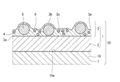
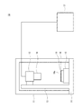
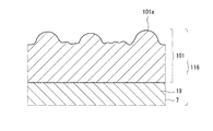
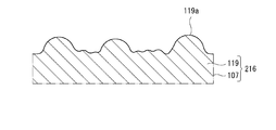
- FIG. 2 is a schematic sectional view of the pen input device according to the first embodiment. It is a schematic diagram of a glare inspection machine. It is a typical sectional view of the pen input device concerning a 2nd embodiment. It is a typical sectional view of the pen input device concerning a 3rd embodiment.
- FIG. 1 is a schematic sectional view of the pen input device 16 according to the first embodiment.
- the pen input device 16 includes a device unit 7 and a surface material 1 for a pen input device (hereinafter, simply referred to as a surface material 1).
- the device unit 7 has a display 19.
- the device unit 7 is, for example, a smartphone, but is not limited thereto.
- the surface material 1 includes, for example, a sheet-like base member 2 and a coat layer 3 that covers one surface of the base member 2.
- the surface material 1 has light transmittance, and the total light transmittance is set to a value in the range of 88% to 100% as an example.
- the surface material 1 is a film here, its thickness is not limited. Therefore, the surface material 1 may be, for example, a plate member.
- the base member 2 is a transparent member, supports the coat layer 3 on one surface, and is mounted on the display surface 19a of the display 19 of the device unit 7 on the other surface.
- the material of the base member 2 is, for example, polyethylene terephthalate (PET), but is not limited thereto.
- PET polyethylene terephthalate
- the base member 2 is a film here, its thickness is not limited. Therefore, the base member 2 may be, for example, a plate member.
- the coat layer 3 is a transparent layer, and is disposed so as to cover one surface of the base member 2 (the upper surface 2a located on the side opposite to the display surface 19a).
- the coat layer 3 has an uneven surface 3a arranged on the side opposite to the base member 2 side.
- the uneven surface 3a is an input surface input by a pen for a pen input device.
- the material of the tip portion of the pen can be appropriately set, and is, for example, polyacetal (POM).
- the thickness of the coat layer 3 is not limited.
- the surface material 1 irregularities having an absolute height of 1.0 ⁇ m or more as measured by a scanning white interference microscope are formed on the uneven surface 3a, and the absolute height of the uneven surface 3a as measured by the microscope is reduced.
- the value of the surface roughness (arithmetic mean roughness) Sa in the range of less than 1.0 ⁇ m is set to a value in the range of 0.10 or more and 0.16 or less.
- the surface roughness Sa referred to here is obtained by expanding the arithmetic average roughness Ra defined by JIS B # 0601 three-dimensionally and dividing the volume of a portion surrounded by the curved surface forming the surface shape and the average surface by the measured area. Is defined as Further, according to the scanning white light interference microscope, the surface shape of the uneven surface 3a can be confirmed without contact, and the surface roughness Sa can be measured.
- the surface material 1, the rolling circle maximum waviness W EM of the uneven surface 3a as measured by a surface roughness shape measuring machine is set to a value in the range of 8.0 to 12.0.
- the surface material 1 has a standard deviation of the luminance distribution of the display 19 when mounted on the surface of the display 19 set to a value in a range of 0 or more and 10 or less. This measurement can be performed in accordance with, for example, JIS B 0610.
- the coat layer 3 of the present embodiment has a base portion 4 extending along the upper surface 2 a of the base member 2, and first particles 5 and second particles 6 dispersed in the base portion 4.
- the base portion 4 is made of a resin material.
- the first particles 5 are acrylic particles
- the second particles 6 are silica particles (nano-silica particles).
- the average particle size of the first particles 5 is set to a value in a range from 10 ⁇ m to 15 ⁇ m.
- the average particle diameter of the second particles 6 is set to a value in a range from 0.4 ⁇ m to less than 0.6 ⁇ m.
- the average particle diameter of the second particles 6 is set to 0.5 ⁇ m.
- the average particle size referred to in this specification refers to a 50% volume average particle size in a Coulter counter method.
- the haze value of the coat layer 3 is set to a value in the range of 8% or more and 39% or less.
- the particles 5 and 6 are held in the base portion 4 in a state of being dispersed inside the base portion 4 and covered by the base portion 4.
- the base portion 4 covers the particles 5 and 6 and partially protrudes at a position corresponding to the particles 5 and 6 on the side opposite to the base member 2 side.
- the base portion 4 has protrusions 3b and 3c.
- the protruding portion 3 b protrudes from a peripheral area of the position at a position corresponding to the first particle 5 to a side opposite to the base member 2.
- the protruding portion 3 c protrudes from a peripheral region of the position on the opposite side to the base member 2 at a position corresponding to the second particle 6.
- the protrusion 3b is larger than the protrusion 3c.
- a plurality of protrusions 3b and 3c are dispersedly arranged along the uneven surface 3a of the coat layer 3.
- at least one protrusion 3c is arranged on the uneven surface 3a of the coat layer 3 between a pair of adjacent protrusions 3b.
- the dynamic friction coefficient of the surface (the uneven surface 3a) of the surface material 1 opposite to the display 19 side is set to a value in the range of 0.24 or more and 0.26 or less. Further, as described above, the standard deviation of the luminance distribution of the display 19 when the surface material 1 is mounted on the surface of the display 19 (display surface 19a) is set to a value in the range of 0 to 10.
- the surface material 1 has the uneven surface 3a input by the pen. Then, irregularities having an absolute height of 1.0 ⁇ m or more as measured by a scanning white interference microscope are formed on the uneven surface 3a, and the absolute height of the uneven surface 3a as measured by the microscope is 1.0 ⁇ m.
- the value of the surface roughness Sa in the range of less than is set to a value in the range of 0.10 or more and 0.16 or less.
- the unevenness having an absolute height of 1.0 ⁇ m or more as measured by the microscope is formed on the uneven surface 3a, whereby the unevenness having an appropriate size is formed on the uneven surface 3a. For this reason, when inputting to the uneven surface 3a with the pen, the vibration and acceleration of the pen are close to the vibration and acceleration of the pen when writing on the paper with the pen, and an excellent writing quality close to the writing quality of paper is obtained. .
- the value of the surface roughness Sa in the range where the absolute height of the uneven surface 3a measured by the microscope is less than 1.0 ⁇ m is set to a value in the range of 0.10 to 0.16.
- minute unevenness is formed on the uneven surface 3a, and the lens effect due to the unevenness of the uneven surface 3a is reduced.
- the surface material 1 is mounted on the display 19, the occurrence of glare of the display 19 due to the enlargement of the pixels due to the lens effect due to the unevenness of the uneven surface 3a is suppressed.
- the glare of the display 19 is relatively large when the resolution of the display 19 is 200 ppi or more. Therefore, by applying the surface material 1 to the device unit 7 including the display 19 having such high-definition pixels, the glare of the display 19 can be more appropriately suppressed.
- the surface material 1 of the present embodiment includes a sheet-shaped base member 2 and a coat layer 3 that covers one surface of the base member 2, and is disposed on the opposite side of the coat layer 3 from the base member 2 side.
- the finished surface is the uneven surface 3a.
- the coat layer 3 by changing the coat layer 3 while using the common base member 2, it is possible to easily form the uneven surface 3a having a desired surface shape. Further, the functions of the base member 2 and the coat layer 3 can be easily exhibited.
- the coat layer 3 of the present embodiment has a base portion 4 extending along the upper surface 2 a of the base member 2, and first particles 5 and second particles 6 dispersed in the base portion 4.
- the average particle size of the particles 5 is set to a value in the range of 10 ⁇ m to 15 ⁇ m
- the average particle size of the second particles 6 is set to a value in the range of 0.4 ⁇ m to less than 0.6 ⁇ m.
- the first particles 5 are acrylic particles
- the second particles 6 are silica particles.
- the haze value of the coat layer 3 is set to a value in the range of 8% or more and 39% or less.
- the coating layer 3 has the second particles 6, it is possible to provide the uneven surface 3a with minute unevenness which is unlikely to induce glare of the display, and it is possible to prevent the reflection of the external light on the uneven surface 3a satisfactorily.
- 3a can be provided with anti-glare properties.
- the standard deviation of the luminance distribution of the display 19 when mounted on the surface of the display 19 is set to a value in the range of 0 or more and 10 or less.
- the value of the standard deviation of the luminance distribution of the display 19 indicates the degree of variation of the bright spots on the display 19, and is an objective index capable of quantitatively evaluating the glare of the display 19. Therefore, by setting the value of the standard deviation to a value within the range of 0 or more and 10 or less, glare of the display 19 through the surface material 1 can be favorably suppressed.
- the surface material 1 the rolling circle maximum waviness W EM of the uneven surface 3a as determined by a scanning white light interference microscope is set to a value in the range of 8.0 to 12.0.
- rolling circle maximum waviness W EM of uneven surfaces 3a when entering the surface material 1 with a pen, when the pen leaves stuck with each holding area, the amplitude of the pen vibration of by the vibration pen And the pen acceleration becomes close to the amplitude of the pen vibration and the pen acceleration due to the vibration of the pen when writing on the paper with the pen, so that the writing quality closer to the writing quality of the paper is obtained. Therefore, it is possible to obtain the surface material 1 having more excellent writing taste.
- the surface material 1 has a transmission image definition of an optical comb width of 0.5 mm set to a value in the range of 45% to 100%. Thereby, the glare of the display 19 can be suppressed while having excellent writing quality, and the surface material 1 that can transmit the emitted light of the display 19 well can be realized.
- the average particle size of the first particles 5 is less than 10 ⁇ m, the writing quality of the uneven surface 3a may be reduced, and when the average particle size is more than 15 ⁇ m, the scratch resistance may be reduced. pay attention to.
- the average particle size of the second particles 6 is less than 0.4 ⁇ m, it is noted that the effect of suppressing the glare of the display 19 and the effect of the anti-glare property may be reduced.
- the average particle diameter of the second particles 6 is 0.6 ⁇ m or more, it is noted that the glare of the display 19 may be increased.
- the haze value of the coat layer 3 is less than 8%, it is noted that the effect of the antiglare property of the display 19 may be reduced. Also, when the haze value of the coat layer 3 is a value exceeding 39%, the visibility of the display 19 may be reduced (character blur or the like may occur), so that attention is paid. In addition, when the transmitted image definition of the surface material 1 with an optical comb width of 0.5 mm is less than 45%, the image display performance of the display 19 via the surface material 1 may be reduced.
- the pen input device 16 is a pen input device including a display 19 and an input surface (an uneven surface 3 a) input by the pen at a position overlapping the display area of the display 19.
- the dynamic friction coefficient is set to a value in the range of 0.24 or more and 0.26 or less, and the standard deviation of the luminance distribution of the display 19 is set to a value in the range of 0 or more and 10 or less.
- FIG. 2 is a schematic diagram of the glare inspection machine 10.
- the glare inspection machine 10 is an apparatus for evaluating the glare of the display 19 of the pen input device 16 having a pen input device surface material such as the surface material 1 mounted on the surface.
- the glare inspection machine 10 includes a housing 11, an imaging device 12, a holding unit 13, an imaging device mount 14, a device mount 15, and an image processing device 17.
- "film glare inspection machine” manufactured by Komatsu NTC Co., Ltd. can be mentioned.
- the housing 11 has a dark room for capturing an image of the display 19 by the imaging device 12.
- the housing 11 accommodates the imaging device 12, the holding unit 13, the imaging device mount 14, the device mount 15, and the pen input device 16 to be evaluated.
- the imaging device 12 is, for example, an area camera having a lens 18 and an imaging element, and captures an image displayed on the display 19.
- the imaging device 12 is connected to the image processing device 17 and is held by the holding unit 13 so that the lens 18 and the display 19 face each other. Image data captured by the imaging device 12 is transmitted to the image processing device 17.
- the holding unit 13 extends in the up-down direction, and holds the imaging device 12 while being fixed to the imaging device base 14 at the lower end.
- the holding unit 13 holds the imaging device 12 such that the relative distance between the display 19 and the lens 18 can be changed by relatively moving the imaging device 12 relative to the pen input device 16 in the vertical direction.
- the pen input device 16 is placed on the upper surface of the device base 15 with the display 19 with the surface material attached facing the imaging device 12.
- the device mount 15 supports the display 19 on which the surface material is mounted so that the surface of the display 19 faces the imaging device 12 and is on a horizontal plane, and moves the pen input device 16 relatively to the imaging device 12 in the vertical direction. .
- the glare inspection machine 10 adjusts the relative distance between the imaging device 12 and the display 19 to display an image per unit pixel (for example, one pixel) of the imaging device of the imaging device 12 and display the image on the display 19.
- the pixel size of the image is adjusted.
- the image processing device 17 performs data processing of image data captured by the imaging device 12. Specifically, the image processing device 17 obtains a standard deviation of the luminance of the display 19 from the image data captured by the imaging device 12.
- the image processing device 17 includes an input unit to which image data captured by the imaging device 12 is input, an image processing unit that performs image processing on the input image data, and a display device or printout that outputs a result processed by the image processing unit.
- An output unit for outputting to a device or the like is provided.
- the method of adjusting the pixel size of an image captured per unit pixel (for example, one pixel) of the image sensor when the image displayed on the display 19 is captured by the image capturing device 12 is as follows.
- the method of changing the focal length of the imaging device 12 may be used.
- an adjustment step of adjusting the pixel size of the display 19 on which the surface material to be imaged per unit pixel of the imaging device of the imaging device 12 is mounted is performed.
- the adjustment step there is no bright line due to pixels in the image captured by the imaging device 12 or even if there is a bright line due to pixels in the image captured by the imaging device 12 depending on the number of effective pixels of the imaging device of the imaging device 12, which affects the evaluation of the glare of the display 19.
- the relative distance between the imaging device 12 and the display 19 on which the surface material is mounted is adjusted to the extent that the image is not given.
- the relative distance between the imaging device 12 and the pen input device 16 is set in consideration of the usage mode of the pen input device 16 (for example, the relative distance between the user's eyes and the surface of the display 19). It is desirable.
- a setting step of setting a measurement area for evaluating the glare of the display 19 on which the surface material is mounted is performed.
- the measurement area is appropriately set according to, for example, the size of the display 19 and the like.
- an imaging step of imaging the measurement area of the display 19 on which the surface material is mounted by the imaging device 12 is performed.
- at least one of the exposure time of the imaging device 12 or the luminance of all the pixels of the display 19 is set so that image data is obtained as a grayscale image with 8-bit gradation display and an average luminance of 170 gradations. adjust.
- Image data captured in the imaging step is input to the image processing device 17.
- the image data is subjected to image processing in a grayscale image state, for example.
- the image processing device 17 After the imaging step, the image processing device 17 performs a calculation step of using the image data to determine a variation in luminance in a measurement area of the display 19 on which the surface material is mounted. In this calculation step, the variation in luminance is quantified as a standard deviation of the luminance distribution.
- the glare of the display 19 with the surface material attached thereto increases as the variation in luminance of the display 19 with the surface material attached increases.
- the adjustment step since the bright line of the display 19 with the surface material is adjusted so as not to affect the evaluation of the glare of the display 19, the uneven brightness due to the bright line is suppressed, and the accurate evaluation of the glare of the display 19 is performed. It can be carried out.
- the standard deviation (glitter ⁇ ) of the luminance distribution of the display 19 when the surface material is mounted on the surface is obtained, and the glare of the display 19 can be evaluated based on the value.
- other embodiments will be described focusing on differences from the first embodiment.
- FIG. 3 is a schematic sectional view of the pen input device 116 according to the second embodiment.
- the pen input device 116 includes a pen input device surface material 101 having a single structure and arranged on the display 19.
- the surface material 101 has an uneven surface 101a which is an input surface for input by a pen.
- the uneven surface 101a has the same surface shape as the uneven surface 3a.
- Such a surface material 101 is, for example, transferred to a surface of a sheet-like uncured material (eg, a resin material) supported by a support member using a shaping member such as a shaping roll, and then transferred to the surface. It is formed by curing a material and peeling it from a support member. Alternatively, the surface material 101 is formed by performing a surface treatment such as sandblasting on the surface of the sheet member.
- a sheet-like uncured material eg, a resin material
- a shaping member such as a shaping roll
- FIG. 4 is a schematic sectional view of a pen input device 216 according to the third embodiment.
- the display 119 included in the device unit 107 of the pen input device 216 has an uneven surface 119a which is an input surface to be input by a pen.
- the outermost layer of the display 119 also serves as a pen input device surface material.
- the uneven surface 119a has the same surface shape as the uneven surface 3a.
- the outermost layer portion of the display 119 is made of, for example, a glass material.
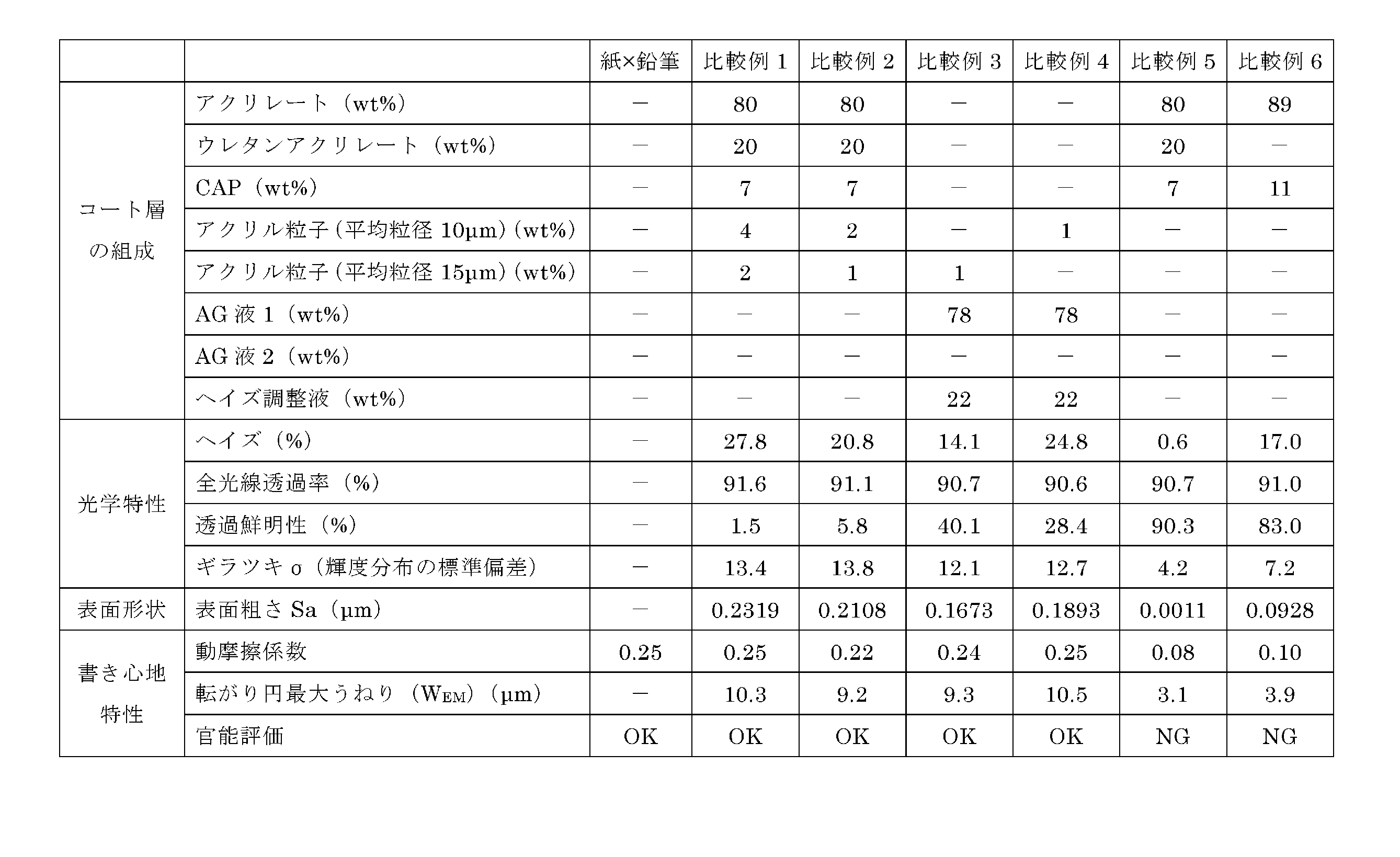
- Examples 1 to 5 correspond to the surface material 1 according to the first embodiment in which the coat layer 3 has the first particles 5 (acrylic particles) and the second particles 6 (nano-silica particles).
- Comparative Examples 1 and 2 correspond to a surface material in which the coat layer has no particles other than the first particles 5.
- Comparative Examples 3 and 4 correspond to surface materials in which the coating layer has no particles other than the first particles 5 and nano-silica particles having an average particle diameter of 0.6 ⁇ m.
- Comparative Examples 5 and 6 correspond to surface materials in which the coat layer has no particles.
- the “AG liquid 1” in Tables 1 and 2 contains nanosilica particles (average particle diameter 0.6 ⁇ m), has a solid content of 54.5%, and has methoxypropanal (PGM), butyl acetate, and One containing polyethylene glycol methyl ether acetate (PGMEA) was used.
- the “AG liquid 2” in Tables 1 and 2 contains nanosilica particles (average particle diameter 0.5 ⁇ m) as the second particles 6, has a solid content of 50.0%, and has methoxypropanal (PGM) as a solvent. ), Butyl acetate, and polyethylene glycol methyl ether acetate (PGMEA).
- the haze value and total light transmittance of each surface material were measured using a haze meter (NDH-5000W, manufactured by Nippon Denshoku Co., Ltd.) in accordance with JIS K7105.
- the transmission clarity (transmission image clarity) of each surface material was measured using a mapping measuring device (ICM-1T, manufactured by Suga Test Instruments Co., Ltd.) in accordance with JIS K7105.
- the glare ⁇ when each surface material was mounted on the display 19 was measured based on the glare evaluation method described above.
- a smartphone with a resolution of 441 ppi (“Galaxy @ S4” manufactured by Samsung Electronics Co., Ltd.) was used.
- At the time of this measurement at least one of the exposure time of the imaging device 12 and the luminance of all pixels of the display 19 is determined so that image data is obtained as a grayscale image with 8-bit gradation display and an average luminance of 170 gradations. It was adjusted.
- the dynamic friction coefficient of each surface material was measured using a static / dynamic friction measuring device “Handy Tribomaster TL201Ts” manufactured by Trinity Lab.
- a pen whose pen tip material is polyacetal pen tip diameter 0.8 mm
- the angle of the pen with respect to the uneven surface (input surface) of each surface material was set to 45 °
- the pen tip to the surface was performed by relatively moving the pen and the uneven surface (input surface) at a moving speed of 50 mm / sec while applying a load of 200 g to the uneven surface (input surface) of the material coat layer.
- the circular maximum waviness W EM rolling in uneven surface of the surface material (input face), JIS B was measured using a surface roughness shape measuring instrument ("Surfcom 1400G” manufactured by Tokyo Seimitsu Co., Ltd.).
- the surface roughness Sa of the uneven surface (input surface) in the range where the absolute height of the uneven surface (input surface) of each surface material is less than 1.0 ⁇ m is determined by a scanning white interference microscope (manufactured by Hitachi High-Tech Science Corporation). , "VertScan").
- the absolute height is 1 in the image of the uneven surface (input surface) of the surface material captured by the scanning white interference microscope. The measurement was performed by selecting a region of the uneven surface of less than 0.0 ⁇ m.
- Examples 1 to 5 had a sensory evaluation equivalent to Comparative Examples 1 to 4, and were found to have excellent writing quality equivalent to Comparative Examples 1 to 4. It is considered that the reason for this is that the coat layers of Examples 1 to 5 have acrylic particles (first particles 5) similarly to the coat layers of Comparative Examples 1 to 4.
- Examples 1 to 5 the glare ⁇ value was reduced as compared with Comparative Examples 1 to 4, and the glare of the display 19 could be suppressed.
- the coat layers 3 of Examples 1 to 5 contain the second particles 6 and have the surface roughness Sa in the range where the absolute height of the uneven surface 3a is less than 1.0 ⁇ m. It is conceivable that the lens effect of the uneven surface 3a that enlarges the pixels of the display 19 was reduced by suppressing the surface roughness compared to the surface roughness Sa.
- Examples 1 to 5 had the same total light transmittance as Comparative Examples 1 to 6, and it was found that the images on the display 19 could be transmitted well.
- Comparative Examples 1 and 2 correspond to the surface material of the conventional pen input device.
- the writing quality of the input surface is excellent because the coating layer has the first particles 5, but the coating layer has the second particles 6. It has been found that there is a possibility that glare of the display 19 may occur due to the absence of. Further, the coating layers of Comparative Examples 3 and 4 have nano-silica particles having an average particle diameter of 0.6 ⁇ m in addition to the first particles 5, but the glare of the display 19 is not sufficiently suppressed by such nano-silica particles. I understood.
- Comparative Examples 5 and 6 although the glare ⁇ value was significantly smaller than those in Examples 1 to 5 and Comparative Examples 1 to 4, the value of the rolling circle maximum undulation W EM was significantly smaller and the sensory evaluation was not excellent. I found out. The reason for this is that the coating layers of Comparative Examples 5 and 6 do not contain any particles, so that the glare of the display 19 can be suppressed, but the unevenness of the input surface in contact with the pen is significantly suppressed, and the writing quality is reduced. It is considered.
- the transmitted image sharpness with an optical comb width of 0.5 mm is set to a value in a range of 45% to 100%. Turned out to be desirable.
- the haze value of the coat layer 3 is set to a value in the range of 8% to 39%. I understood. In order to obtain more excellent writing feeling is rolling circle maximum waviness W EM of the uneven surface 3a as measured by the microscope, to be set to a value in the range of 8.0 to 12.0 It turned out to be desirable.
- the pen input device 16 of the first embodiment was manufactured as an example device.
- the device unit 7 a smartphone with a resolution of 441 ppi (“Galaxy” manufactured by Samsung Electronics Co., Ltd.) S4 "), and the surface material 1 of Example 1 was used as the surface material 1.
- an adhesive film “PX38T02G50 / PDS1T” manufactured by Panac Co., Ltd. substitution: OCA layer (transparent optical adhesive layer: thickness 25 ⁇ m) / PET layer (thickness 38 ⁇ m) / silicon adhesive layer (thickness 50 ⁇ m)
- the surface material 1 was formed as a pressure-sensitive adhesive film by attaching the adhesive surface (OCA layer side) of the three-layer structure) to the base member 2 of the surface material 1 of Example 1. This surface material 1 was adhered to the surface of the display 19 on the other adhesive surface (the silicon adhesive layer side). Thereby, the surface material 1 was mounted on the device unit 7.
- the average dynamic friction coefficient of the uneven surface 3a was measured using a static / dynamic friction measuring device “Handy Tribomaster TL201Ts” manufactured by Trinity Lab.
- a pen whose pen tip is made of polyacetal pen tip diameter 0.8 mm
- the angle of the pen with respect to the irregular surface 3a was set to 45 °
- the irregular surface in the coat layer of the surface material from the pen tip was set.
- the pen and the uneven surface 3a are moved relative to each other three times at a moving speed of 50 mm / sec and a moving distance of 50 mm while a load of 50 g is applied to the 3a, and the average value of the measured dynamic friction coefficients is the average dynamic friction coefficient.
- the average dynamic friction coefficient of the device of the example obtained from the measurement results was the same as the measured value of the dynamic friction coefficient of the device of Example 1.
- the evaluation was almost the same as the evaluation of the examples 1 to 5.
Landscapes
- Physics & Mathematics (AREA)
- General Physics & Mathematics (AREA)
- Optics & Photonics (AREA)
- Engineering & Computer Science (AREA)
- Chemical & Material Sciences (AREA)
- Dispersion Chemistry (AREA)
- General Engineering & Computer Science (AREA)
- Theoretical Computer Science (AREA)
- Human Computer Interaction (AREA)
- Optical Elements Other Than Lenses (AREA)
- Devices For Indicating Variable Information By Combining Individual Elements (AREA)
- Position Input By Displaying (AREA)
- Laminated Bodies (AREA)
Abstract
Description
(第1実施形態)
[ペン入力デバイス用表面材]
図1は、第1実施形態に係るペン入力デバイス16の模式断面図である。図1に示すように、ペン入力デバイス16は、デバイスユニット7と、ペン入力デバイス用表面材1(以下、単に表面材1と称する。)を備える。デバイスユニット7は、ディスプレイ19を有する。デバイスユニット7は、一例としてスマートフォンであるが、これに限定されない。
図2は、ギラツキ検査機10の概略図である。ギラツキ検査機10は、表面に表面材1等のペン入力デバイス用表面材を装着したペン入力デバイス16におけるディスプレイ19のギラツキを評価する装置である。ギラツキ検査機10は、筐体11、撮像装置12、保持部13、撮像装置用架台14、デバイス用架台15、及び画像処理装置17を備える。市販されているギラツキ検査機10としては、コマツNTC(株)製「フィルムギラツキ検査機」が挙げられる。
画像処理装置17は、撮像装置12によって撮像された画像データのデータ処理を行う。具体的に画像処理装置17は、撮像装置12によって撮像された画像データから、ディスプレイ19の輝度の標準偏差を求める。
以下、ギラツキ検査機10を用いたディスプレイ19のギラツキ評価方法について説明する。このギラツキ評価方法においては、評価の便宜上、ペン入力デバイス16のディスプレイ面19aに表面材1等のペン入力デバイス用表面材を装着したディスプレイ19を予め一色(一例として緑色)に均一発光させて表示させる。
図3は、第2実施形態に係るペン入力デバイス116の模式的な断面図である。ペン入力デバイス116は、ディスプレイ19に重ねて配置された単一構造を有するペン入力デバイス用表面材101を備える。この表面材101は、ペンにより入力される入力面である凹凸面101aを有する。凹凸面101aは、凹凸面3aと同様の表面形状を有する。
[試験1]
以下の表1,2に示す組成を有する実施例1~5及び比較例1~6の各ペン入力デバイス用表面材を作製した。表1,2中の「アクリル粒子」は、第1粒子5に相当する。また表1,2中の「CAP」は、セルロースアセテートプロピオネートであり、「表面粗さSa」は、凹凸面の絶対高さが1.0μm未満の範囲を指す。
610に準拠し、表面粗さ形状測定機(東京精密(株)製、「サーフコム1400G」)を用いて測定した。また、各表面材の凹凸面(入力面)の絶対高さが1.0μm未満の範囲における凹凸面(入力面)の表面粗さSaは、走査型白色干渉顕微鏡(日立ハイテクサイエンス(株)製、「VertScan」)を用いて測定した。

第1実施形態のペン入力デバイス16を実施例デバイスとして作製した。デバイスユニット7として、解像度441ppiのスマートフォン(サムスン電子社製「Galaxy
S4」)を用い、表面材1として、実施例1の表面材1を用いた。
2 ベース部材
3 コート層
3a,101a,119a 凹凸面
4 ベース部
5 第1粒子
6 第2粒子
16,116,216 ペン入力デバイス
19,119 ディスプレイ
Claims (9)
- ペンにより入力される凹凸面を有し、
走査型白色干渉顕微鏡により測定したときの絶対高さが1.0μm以上の凹凸が前記凹凸面に形成され、且つ、前記顕微鏡により測定したときの前記凹凸面の前記絶対高さが1.0μm未満の範囲における表面粗さSaの値が、0.10以上0.16以下の範囲の値に設定されている、ペン入力デバイス用表面材。 - シート状のベース部材と、
前記ベース部材の一方の面を被覆するコート層とを備え、
前記コート層の前記ベース部材側とは反対側に配置された面が、前記凹凸面である、請求項1に記載のペン入力デバイス用表面材。 - 前記コート層は、前記ベース部材の前記一方の面に沿って延びるベース部と、前記ベース部中に分散された第1粒子と第2粒子とを有し、
前記第1粒子の平均粒径が、10μm以上15μm以下の範囲の値に設定され、
前記第2粒子の平均粒径が、0.4μm以上0.6μm未満の範囲の値に設定されている、請求項2に記載のペン入力デバイス用表面材。 - 前記第1粒子がアクリル粒子であり、前記第2粒子がシリカ粒子である、請求項3に記載のペン入力デバイス用表面材。
- 前記コート層のヘイズ値が8%以上39%以下の範囲の値に設定されている、請求項2~4のいずれか1項に記載のペン入力デバイス用表面材。
- ディスプレイの表面に装着したときの前記ディスプレイの輝度分布の標準偏差が、0以上10以下の範囲の値に設定されている、請求項1~5のいずれか1項に記載のペン入力デバイス用表面材。
- 表面粗さ形状測定機により測定したときの前記凹凸面の転がり円最大うねりWEMが、8.0以上12.0以下の範囲の値に設定されている、請求項1~6のいずれか1項に記載のペン入力デバイス用表面材。
- 光学櫛幅0.5mmの透過像鮮明度が、45%以上100%以下の範囲の値に設定されている、請求項1~7のいずれか1項に記載のペン入力デバイス用表面材。
- ディスプレイと、前記ディスプレイの表示領域と重なる位置でペンにより入力される入力面とを備えるペン入力デバイスであって、
前記入力面の動摩擦係数が、0.24以上0.26以下の範囲の値に設定され、前記ディスプレイの輝度分布の標準偏差が、0以上10以下の範囲の値に設定されている、ペン入力デバイス。
Priority Applications (4)
| Application Number | Priority Date | Filing Date | Title |
|---|---|---|---|
| JP2020528993A JP6955104B2 (ja) | 2018-07-03 | 2019-07-02 | ペン入力デバイス用表面材及びペン入力デバイス |
| CN201980037871.1A CN112236744B (zh) | 2018-07-03 | 2019-07-02 | 笔输入设备用表面材料及笔输入设备 |
| US17/253,893 US12320994B2 (en) | 2018-07-03 | 2019-07-02 | Surface material for pen input device and pen input device |
| US19/197,615 US20250264641A1 (en) | 2018-07-03 | 2025-05-02 | Surface material for pen input device and pen input device |
Applications Claiming Priority (2)
| Application Number | Priority Date | Filing Date | Title |
|---|---|---|---|
| JP2018-126568 | 2018-07-03 | ||
| JP2018126568 | 2018-07-03 |
Related Child Applications (2)
| Application Number | Title | Priority Date | Filing Date |
|---|---|---|---|
| US17/253,893 A-371-Of-International US12320994B2 (en) | 2018-07-03 | 2019-07-02 | Surface material for pen input device and pen input device |
| US19/197,615 Division US20250264641A1 (en) | 2018-07-03 | 2025-05-02 | Surface material for pen input device and pen input device |
Publications (1)
| Publication Number | Publication Date |
|---|---|
| WO2020009083A1 true WO2020009083A1 (ja) | 2020-01-09 |
Family
ID=69060391
Family Applications (1)
| Application Number | Title | Priority Date | Filing Date |
|---|---|---|---|
| PCT/JP2019/026201 Ceased WO2020009083A1 (ja) | 2018-07-03 | 2019-07-02 | ペン入力デバイス用表面材及びペン入力デバイス |
Country Status (5)
| Country | Link |
|---|---|
| US (2) | US12320994B2 (ja) |
| JP (3) | JP6955104B2 (ja) |
| CN (1) | CN112236744B (ja) |
| TW (1) | TWI722469B (ja) |
| WO (1) | WO2020009083A1 (ja) |
Families Citing this family (2)
| Publication number | Priority date | Publication date | Assignee | Title |
|---|---|---|---|---|
| TWI800307B (zh) * | 2022-03-17 | 2023-04-21 | 元太科技工業股份有限公司 | 觸控板的檢測治具與觸控板的檢測方法 |
| JP2026053926A (ja) * | 2024-09-13 | 2026-03-26 | 株式会社ダイセル | 積層フィルム、積層シート及び画像表示装置 |
Citations (9)
| Publication number | Priority date | Publication date | Assignee | Title |
|---|---|---|---|---|
| JP2007164206A (ja) * | 2007-01-11 | 2007-06-28 | Toppan Printing Co Ltd | 防眩性ハードコートフィルム |
| JP2010173234A (ja) * | 2009-01-30 | 2010-08-12 | Toppan Printing Co Ltd | ハードコートフィルム |
| JP2012088693A (ja) * | 2010-09-22 | 2012-05-10 | Nitto Denko Corp | 光学フィルムの製造方法 |
| JP2012252038A (ja) * | 2011-05-31 | 2012-12-20 | Daicel Corp | 光学フィルム及びその製造方法 |
| JP2013092782A (ja) * | 2007-08-22 | 2013-05-16 | Tomoegawa Paper Co Ltd | 光学積層体 |
| WO2016158269A1 (ja) * | 2015-04-02 | 2016-10-06 | 株式会社ダイセル | 透明積層フィルム |
| JP2017040834A (ja) * | 2015-08-21 | 2017-02-23 | コニカミノルタ株式会社 | 光学シート及び光学シートの製造方法 |
| JP2017508828A (ja) * | 2014-01-15 | 2017-03-30 | スリーエム イノベイティブ プロパティズ カンパニー | アルコキシ化マルチ(メタ)アクリレートモノマーを含むハードコート及び表面処理されたナノ粒子 |
| WO2017154095A1 (ja) * | 2016-03-08 | 2017-09-14 | 株式会社ワコム | ペン入力装置用シート及びペン入力装置用シートの製法 |
Family Cites Families (17)
| Publication number | Priority date | Publication date | Assignee | Title |
|---|---|---|---|---|
| JP2004259256A (ja) | 2003-02-05 | 2004-09-16 | Nitto Denko Corp | 透明積層体、ペン入力画像表示装置および画像表示方法 |
| JP2010039170A (ja) | 2008-08-05 | 2010-02-18 | Sumitomo Chemical Co Ltd | 感圧接着剤付き光学フィルム、積層光学部材及び画像表示装置 |
| JP6196164B2 (ja) * | 2013-01-09 | 2017-09-13 | 株式会社ダイセル | ペン入力デバイス |
| JP6151611B2 (ja) | 2013-09-10 | 2017-06-21 | 株式会社ダイセル | 透明触感フィルム及びその製造方法 |
| JP6156647B2 (ja) * | 2013-12-05 | 2017-07-05 | コニカミノルタ株式会社 | ペン入力装置用フィルム |
| JP6349126B2 (ja) * | 2014-03-31 | 2018-06-27 | 株式会社ダイセル | ペン入力デバイス用透明積層フィルム及びその製造方法 |
| JP6476582B2 (ja) | 2014-04-23 | 2019-03-06 | 大日本印刷株式会社 | 積層体の製造方法、積層体、偏光板及び画像表示装置 |
| JP2016018333A (ja) | 2014-07-07 | 2016-02-01 | 旭硝子株式会社 | ペン入力装置用のカバーガラスおよびその製造方法 |
| JP6497126B2 (ja) * | 2015-02-26 | 2019-04-10 | 大日本印刷株式会社 | タッチパネル、表示装置及び光学シート、並びに光学シートの選別方法及び光学シートの製造方法 |
| JP6488829B2 (ja) | 2015-03-31 | 2019-03-27 | 大日本印刷株式会社 | タッチパネル付表示装置及び光学フィルム |
| WO2017094784A1 (ja) * | 2015-12-04 | 2017-06-08 | 大日本印刷株式会社 | タッチパネルペン用筆記シート、タッチパネル、タッチパネルシステム及び表示装置、並びにタッチパネルペン用筆記シートの選別方法 |
| US10732733B2 (en) * | 2015-12-07 | 2020-08-04 | Dai Nippon Printing Co., Ltd. | Writing sheet for touch panel pen, touch panel, touch panel system, display device, and method for selecting writing sheet for touch panel pen |
| JP2016118788A (ja) | 2015-12-25 | 2016-06-30 | 大日本印刷株式会社 | 防眩フィルム、偏光板、液晶パネル、および画像表示装置 |
| JP6790524B2 (ja) | 2016-07-08 | 2020-11-25 | 大日本印刷株式会社 | タッチパネルペン用筆記シート、タッチパネル、表示装置、及びタッチパネルペン用筆記シートの選別方法 |
| JP6790565B2 (ja) * | 2016-08-05 | 2020-11-25 | 日本電気硝子株式会社 | ペン入力装置、ペン入力装置用ガラス基板及びその製造方法 |
| JP6345220B2 (ja) * | 2016-11-16 | 2018-06-20 | リンテック株式会社 | 書き味向上フィルム |
| JP7000017B2 (ja) * | 2016-11-16 | 2022-01-19 | リンテック株式会社 | 書き味向上フィルム |
-
2019
- 2019-07-02 JP JP2020528993A patent/JP6955104B2/ja active Active
- 2019-07-02 TW TW108123255A patent/TWI722469B/zh active
- 2019-07-02 CN CN201980037871.1A patent/CN112236744B/zh active Active
- 2019-07-02 WO PCT/JP2019/026201 patent/WO2020009083A1/ja not_active Ceased
- 2019-07-02 US US17/253,893 patent/US12320994B2/en active Active
-
2021
- 2021-08-27 JP JP2021139254A patent/JP7177234B2/ja active Active
-
2022
- 2022-11-10 JP JP2022180057A patent/JP7369269B2/ja active Active
-
2025
- 2025-05-02 US US19/197,615 patent/US20250264641A1/en active Pending
Patent Citations (9)
| Publication number | Priority date | Publication date | Assignee | Title |
|---|---|---|---|---|
| JP2007164206A (ja) * | 2007-01-11 | 2007-06-28 | Toppan Printing Co Ltd | 防眩性ハードコートフィルム |
| JP2013092782A (ja) * | 2007-08-22 | 2013-05-16 | Tomoegawa Paper Co Ltd | 光学積層体 |
| JP2010173234A (ja) * | 2009-01-30 | 2010-08-12 | Toppan Printing Co Ltd | ハードコートフィルム |
| JP2012088693A (ja) * | 2010-09-22 | 2012-05-10 | Nitto Denko Corp | 光学フィルムの製造方法 |
| JP2012252038A (ja) * | 2011-05-31 | 2012-12-20 | Daicel Corp | 光学フィルム及びその製造方法 |
| JP2017508828A (ja) * | 2014-01-15 | 2017-03-30 | スリーエム イノベイティブ プロパティズ カンパニー | アルコキシ化マルチ(メタ)アクリレートモノマーを含むハードコート及び表面処理されたナノ粒子 |
| WO2016158269A1 (ja) * | 2015-04-02 | 2016-10-06 | 株式会社ダイセル | 透明積層フィルム |
| JP2017040834A (ja) * | 2015-08-21 | 2017-02-23 | コニカミノルタ株式会社 | 光学シート及び光学シートの製造方法 |
| WO2017154095A1 (ja) * | 2016-03-08 | 2017-09-14 | 株式会社ワコム | ペン入力装置用シート及びペン入力装置用シートの製法 |
Also Published As
| Publication number | Publication date |
|---|---|
| TW202020640A (zh) | 2020-06-01 |
| JPWO2020009083A1 (ja) | 2021-08-02 |
| CN112236744A (zh) | 2021-01-15 |
| JP2023022067A (ja) | 2023-02-14 |
| JP6955104B2 (ja) | 2021-10-27 |
| CN112236744B (zh) | 2024-04-30 |
| TWI722469B (zh) | 2021-03-21 |
| JP2022000766A (ja) | 2022-01-04 |
| US12320994B2 (en) | 2025-06-03 |
| JP7369269B2 (ja) | 2023-10-25 |
| US20210271103A1 (en) | 2021-09-02 |
| US20250264641A1 (en) | 2025-08-21 |
| JP7177234B2 (ja) | 2022-11-22 |
Similar Documents
| Publication | Publication Date | Title |
|---|---|---|
| US20250264641A1 (en) | Surface material for pen input device and pen input device | |
| JP6721794B2 (ja) | 防眩フィルム | |
| TW438965B (en) | Method and apparatus for quantitatively evaluating scintillation and method of producing antiglare film | |
| JP6743305B2 (ja) | 防眩フィルム | |
| JP2022008876A (ja) | 文字ぼけ評価方法、光学部材、および表示装置 | |
| JP6745411B2 (ja) | 防眩フィルム | |
| TWI275853B (en) | Lens module with dust- proof function | |
| JPWO2019026467A1 (ja) | 防眩フィルム | |
| JP2016157387A (ja) | タッチパネル、表示装置及び光学シート、並びに光学シートの選別方法及び光学シートの製造方法 | |
| TWI700187B (zh) | 筆輸入裝置用表面材 | |
| JP5204723B2 (ja) | 点像の鏡面反射光分布測定方法および測定装置 | |
| CN1701273A (zh) | 具有焦点的球面反射屏幕及其制造方法 | |
| JP7121552B2 (ja) | ギラツキ評価装置およびギラツキ評価方法 | |
| US12578507B2 (en) | Antiglare film | |
| TWI735054B (zh) | 筆輸入裝置用表面材料 | |
| WO2017110038A1 (ja) | タッチパネルと、これを用いた表示装置 | |
| JP6881449B2 (ja) | タッチパネルペン用筆記シートの選別方法、タッチパネルシステム、タッチパネルペン用筆記シート、タッチパネル及び表示装置 |
Legal Events
| Date | Code | Title | Description |
|---|---|---|---|
| 121 | Ep: the epo has been informed by wipo that ep was designated in this application |
Ref document number: 19831006 Country of ref document: EP Kind code of ref document: A1 |
|
| DPE1 | Request for preliminary examination filed after expiration of 19th month from priority date (pct application filed from 20040101) | ||
| ENP | Entry into the national phase |
Ref document number: 2020528993 Country of ref document: JP Kind code of ref document: A |
|
| NENP | Non-entry into the national phase |
Ref country code: DE |
|
| 122 | Ep: pct application non-entry in european phase |
Ref document number: 19831006 Country of ref document: EP Kind code of ref document: A1 |
|
| WWG | Wipo information: grant in national office |
Ref document number: 17253893 Country of ref document: US |