WO2020004086A1 - 有機el素子および有機el素子の製造方法 - Google Patents
有機el素子および有機el素子の製造方法 Download PDFInfo
- Publication number
- WO2020004086A1 WO2020004086A1 PCT/JP2019/023742 JP2019023742W WO2020004086A1 WO 2020004086 A1 WO2020004086 A1 WO 2020004086A1 JP 2019023742 W JP2019023742 W JP 2019023742W WO 2020004086 A1 WO2020004086 A1 WO 2020004086A1
- Authority
- WO
- WIPO (PCT)
- Prior art keywords
- organic
- film
- electrode
- sub
- pixel
- Prior art date
- Legal status (The legal status is an assumption and is not a legal conclusion. Google has not performed a legal analysis and makes no representation as to the accuracy of the status listed.)
- Ceased
Links
Images


Classifications
-
- H—ELECTRICITY
- H10—SEMICONDUCTOR DEVICES; ELECTRIC SOLID-STATE DEVICES NOT OTHERWISE PROVIDED FOR
- H10K—ORGANIC ELECTRIC SOLID-STATE DEVICES
- H10K59/00—Integrated devices, or assemblies of multiple devices, comprising at least one organic light-emitting element covered by group H10K50/00
- H10K59/10—OLED displays
- H10K59/12—Active-matrix OLED [AMOLED] displays
-
- G—PHYSICS
- G09—EDUCATION; CRYPTOGRAPHY; DISPLAY; ADVERTISING; SEALS
- G09F—DISPLAYING; ADVERTISING; SIGNS; LABELS OR NAME-PLATES; SEALS
- G09F9/00—Indicating arrangements for variable information in which the information is built-up on a support by selection or combination of individual elements
- G09F9/30—Indicating arrangements for variable information in which the information is built-up on a support by selection or combination of individual elements in which the desired character or characters are formed by combining individual elements
- G09F9/33—Indicating arrangements for variable information in which the information is built-up on a support by selection or combination of individual elements in which the desired character or characters are formed by combining individual elements being semiconductor devices, e.g. diodes
- G09F9/335—Indicating arrangements for variable information in which the information is built-up on a support by selection or combination of individual elements in which the desired character or characters are formed by combining individual elements being semiconductor devices, e.g. diodes being organic light emitting diodes [OLED]
-
- H—ELECTRICITY
- H05—ELECTRIC TECHNIQUES NOT OTHERWISE PROVIDED FOR
- H05B—ELECTRIC HEATING; ELECTRIC LIGHT SOURCES NOT OTHERWISE PROVIDED FOR; CIRCUIT ARRANGEMENTS FOR ELECTRIC LIGHT SOURCES, IN GENERAL
- H05B33/00—Electroluminescent light sources
- H05B33/02—Details
- H05B33/04—Sealing arrangements, e.g. against humidity
-
- H—ELECTRICITY
- H05—ELECTRIC TECHNIQUES NOT OTHERWISE PROVIDED FOR
- H05B—ELECTRIC HEATING; ELECTRIC LIGHT SOURCES NOT OTHERWISE PROVIDED FOR; CIRCUIT ARRANGEMENTS FOR ELECTRIC LIGHT SOURCES, IN GENERAL
- H05B33/00—Electroluminescent light sources
- H05B33/10—Apparatus or processes specially adapted to the manufacture of electroluminescent light sources
-
- H—ELECTRICITY
- H05—ELECTRIC TECHNIQUES NOT OTHERWISE PROVIDED FOR
- H05B—ELECTRIC HEATING; ELECTRIC LIGHT SOURCES NOT OTHERWISE PROVIDED FOR; CIRCUIT ARRANGEMENTS FOR ELECTRIC LIGHT SOURCES, IN GENERAL
- H05B33/00—Electroluminescent light sources
- H05B33/12—Light sources with substantially two-dimensional [2D] radiating surfaces
-
- H—ELECTRICITY
- H05—ELECTRIC TECHNIQUES NOT OTHERWISE PROVIDED FOR
- H05B—ELECTRIC HEATING; ELECTRIC LIGHT SOURCES NOT OTHERWISE PROVIDED FOR; CIRCUIT ARRANGEMENTS FOR ELECTRIC LIGHT SOURCES, IN GENERAL
- H05B33/00—Electroluminescent light sources
- H05B33/12—Light sources with substantially two-dimensional [2D] radiating surfaces
- H05B33/26—Light sources with substantially two-dimensional [2D] radiating surfaces characterised by the composition or arrangement of the conductive material used as an electrode
- H05B33/28—Light sources with substantially two-dimensional [2D] radiating surfaces characterised by the composition or arrangement of the conductive material used as an electrode of translucent electrodes
-
- H—ELECTRICITY
- H10—SEMICONDUCTOR DEVICES; ELECTRIC SOLID-STATE DEVICES NOT OTHERWISE PROVIDED FOR
- H10K—ORGANIC ELECTRIC SOLID-STATE DEVICES
- H10K50/00—Organic light-emitting devices
- H10K50/80—Constructional details
- H10K50/805—Electrodes
-
- H—ELECTRICITY
- H10—SEMICONDUCTOR DEVICES; ELECTRIC SOLID-STATE DEVICES NOT OTHERWISE PROVIDED FOR
- H10K—ORGANIC ELECTRIC SOLID-STATE DEVICES
- H10K50/00—Organic light-emitting devices
- H10K50/80—Constructional details
- H10K50/84—Passivation; Containers; Encapsulations
- H10K50/844—Encapsulations
-
- H—ELECTRICITY
- H10—SEMICONDUCTOR DEVICES; ELECTRIC SOLID-STATE DEVICES NOT OTHERWISE PROVIDED FOR
- H10K—ORGANIC ELECTRIC SOLID-STATE DEVICES
- H10K59/00—Integrated devices, or assemblies of multiple devices, comprising at least one organic light-emitting element covered by group H10K50/00
- H10K59/10—OLED displays
- H10K59/12—Active-matrix OLED [AMOLED] displays
- H10K59/1201—Manufacture or treatment
-
- H—ELECTRICITY
- H10—SEMICONDUCTOR DEVICES; ELECTRIC SOLID-STATE DEVICES NOT OTHERWISE PROVIDED FOR
- H10K—ORGANIC ELECTRIC SOLID-STATE DEVICES
- H10K59/00—Integrated devices, or assemblies of multiple devices, comprising at least one organic light-emitting element covered by group H10K50/00
- H10K59/10—OLED displays
- H10K59/12—Active-matrix OLED [AMOLED] displays
- H10K59/122—Pixel-defining structures or layers, e.g. banks
-
- H—ELECTRICITY
- H10—SEMICONDUCTOR DEVICES; ELECTRIC SOLID-STATE DEVICES NOT OTHERWISE PROVIDED FOR
- H10K—ORGANIC ELECTRIC SOLID-STATE DEVICES
- H10K59/00—Integrated devices, or assemblies of multiple devices, comprising at least one organic light-emitting element covered by group H10K50/00
- H10K59/30—Devices specially adapted for multicolour light emission
- H10K59/35—Devices specially adapted for multicolour light emission comprising red-green-blue [RGB] subpixels
-
- H—ELECTRICITY
- H10—SEMICONDUCTOR DEVICES; ELECTRIC SOLID-STATE DEVICES NOT OTHERWISE PROVIDED FOR
- H10K—ORGANIC ELECTRIC SOLID-STATE DEVICES
- H10K59/00—Integrated devices, or assemblies of multiple devices, comprising at least one organic light-emitting element covered by group H10K50/00
- H10K59/30—Devices specially adapted for multicolour light emission
- H10K59/35—Devices specially adapted for multicolour light emission comprising red-green-blue [RGB] subpixels
- H10K59/353—Devices specially adapted for multicolour light emission comprising red-green-blue [RGB] subpixels characterised by the geometrical arrangement of the RGB subpixels
-
- H—ELECTRICITY
- H10—SEMICONDUCTOR DEVICES; ELECTRIC SOLID-STATE DEVICES NOT OTHERWISE PROVIDED FOR
- H10K—ORGANIC ELECTRIC SOLID-STATE DEVICES
- H10K59/00—Integrated devices, or assemblies of multiple devices, comprising at least one organic light-emitting element covered by group H10K50/00
- H10K59/80—Constructional details
- H10K59/805—Electrodes
-
- H—ELECTRICITY
- H10—SEMICONDUCTOR DEVICES; ELECTRIC SOLID-STATE DEVICES NOT OTHERWISE PROVIDED FOR
- H10K—ORGANIC ELECTRIC SOLID-STATE DEVICES
- H10K59/00—Integrated devices, or assemblies of multiple devices, comprising at least one organic light-emitting element covered by group H10K50/00
- H10K59/80—Constructional details
- H10K59/87—Passivation; Containers; Encapsulations
- H10K59/873—Encapsulations
-
- H—ELECTRICITY
- H10—SEMICONDUCTOR DEVICES; ELECTRIC SOLID-STATE DEVICES NOT OTHERWISE PROVIDED FOR
- H10K—ORGANIC ELECTRIC SOLID-STATE DEVICES
- H10K71/00—Manufacture or treatment specially adapted for the organic devices covered by this subclass
-
- H—ELECTRICITY
- H10—SEMICONDUCTOR DEVICES; ELECTRIC SOLID-STATE DEVICES NOT OTHERWISE PROVIDED FOR
- H10K—ORGANIC ELECTRIC SOLID-STATE DEVICES
- H10K71/00—Manufacture or treatment specially adapted for the organic devices covered by this subclass
- H10K71/60—Forming conductive regions or layers, e.g. electrodes
-
- H—ELECTRICITY
- H10—SEMICONDUCTOR DEVICES; ELECTRIC SOLID-STATE DEVICES NOT OTHERWISE PROVIDED FOR
- H10K—ORGANIC ELECTRIC SOLID-STATE DEVICES
- H10K2102/00—Constructional details relating to the organic devices covered by this subclass
- H10K2102/301—Details of OLEDs
- H10K2102/351—Thickness
Definitions
- a display device using an organic EL element has a structure in which an organic compound layer including at least a light-emitting layer and a second electrode are stacked on a first electrode formed separately for each pixel.
- One pixel is composed of a plurality of sub-pixels such as RGB.
- each sub-pixel As a formation method of each sub-pixel, a method of forming each color using a white light emitting element and an RGB color filter, and a method of forming each color by separately painting each of a red light emitting element, a green light emitting element, and a blue light emitting element There is a method to make it.
- the light-emitting elements of each color are separately coated by a mask deposition method in which a light-emitting layer is deposited for each pixel using a mask, and a printing method in which a light-emitting layer is applied and formed for each pixel using an inkjet head.
- a mask deposition method in which a light-emitting layer is deposited for each pixel using a mask
- a printing method in which a light-emitting layer is applied and formed for each pixel using an inkjet head.
- an etching method in which a light emitting layer formed on the entire surface is patterned for each pixel by etching or the like is used.
- an etching method with high pixel formation accuracy is suitable.
- Patent Literature 1 discloses a technique in which organic EL elements are separately applied by an etching method.
- the organic compound layer of the organic EL element reacts with oxygen or moisture in the outside air, a process gas, a chemical solution, or the like to obtain a characteristic. May be deteriorated. In particular, since the side surface of the organic compound layer is exposed to the outside air or the like, the deterioration is likely to proceed.
- the organic EL element In view of the above circumstances, it is desirable to configure the organic EL element with a structure capable of suppressing deterioration of characteristics.
- the sub-pixels on which the first electrode and the second electrode are stacked with the organic compound layer including at least the light-emitting layer emitting different colors are separated from each other on a plane orthogonal to the stacking direction. At least two or more organic EL elements are provided, and a side surface of the organic compound layer is covered with a different film for each sub-pixel.
- the sub-pixels on which the first electrode and the second electrode are stacked with the organic compound layer including at least the light-emitting layer that emits different colors are arranged on a plane orthogonal to the stacking direction. Forming at least two or more layers separated from each other, and forming a film covering a side surface of the organic compound layer each time the shape of the organic compound layer that emits each color is processed in the formation of the sub-pixel. And a method for manufacturing an organic EL device.
- each sub-pixel since the side surface of the organic compound layer of each sub-pixel is not exposed, it is possible to suppress the organic compound layer from being exposed to outside air, a process gas, a chemical, or the like.
- an organic EL element capable of suppressing deterioration of characteristics.
- the above effects are not necessarily limited, and any of the effects described in the present specification or other effects that can be grasped from the present specification, together with or instead of the above effects. May be played.
- FIG. 1 is a cross-sectional view in a stacking direction of an organic EL element according to an embodiment of the present disclosure. It is a figure showing an example of a manufacturing process of an organic EL element concerning the embodiment. It is a figure showing an example of a manufacturing process of an organic EL element concerning the embodiment. It is a figure showing an example of a manufacturing process of an organic EL element concerning the embodiment. It is a figure showing an example of a manufacturing process of an organic EL element concerning the embodiment. It is a figure showing an example of a manufacturing process of an organic EL element concerning the embodiment. It is a figure showing an example of a manufacturing process of an organic EL element concerning the embodiment. It is a figure showing an example of a manufacturing process of an organic EL element concerning the embodiment.
- FIG. 3 is a diagram illustrating an example of a planar arrangement layout of sub-pixels.
- FIG. 3 is a diagram illustrating an example of a planar arrangement layout of sub-pixels.
- FIG. 3 is a diagram illustrating an example of a planar arrangement layout of sub-pixels.
- FIG. 3 is a diagram illustrating an example of a planar arrangement layout of sub-pixels.
- an outline of an organic EL device according to an embodiment of the present disclosure will be described.
- an organic compound layer including at least a light emitting layer that emits a different color is provided.
- a first electrode and a second electrode are stacked with the organic compound layer interposed therebetween. At least two subpixels having this configuration are provided on a plane orthogonal to the stacking direction and separated from each other.
- an organic EL element In an organic EL element, holes and electrons are injected from the first electrode and the second electrode, respectively, by applying an electric field between the first electrode and the second electrode, and the holes and electrons are injected in the organic compound layer.
- the light emission is performed by combining.
- the organic compound layer In the manufacture of the organic EL element, the organic compound layer is exposed to moisture, oxygen, a process gas, a chemical solution, or the like in the process of sequentially manufacturing each sub-pixel, so that the organic compound layer is deteriorated. There is.
- the organic EL element of the present disclosure suppresses the deterioration of the organic compound layer by covering the side surface of the organic compound layer with a different film for each sub-pixel of each color.
- FIG. 1 is a cross-sectional view schematically illustrating a cross section of an organic EL element according to an embodiment of the present disclosure cut in a stacking direction.
- the laminating direction of each layer in the organic EL element 100 is referred to as a vertical direction. Further, the direction in which the substrate 120 is arranged is expressed as a downward direction, and the direction in which the opposing glass 111 is arranged is expressed as an upward direction.
- the size of some components may be exaggerated for convenience of explanation. Therefore, the relative sizes of the components illustrated in the drawings do not always accurately represent the magnitude relationship between the actual components.
- a region emitting green light was defined as a green light emitting region G
- a region emitting blue light was defined as a blue light emitting region B
- a region emitting red light was defined as a red light emitting region R.
- the sub-pixels formed for each of the regions that emit different colors are a sub-pixel 110G that emits green, a sub-pixel 110B that emits blue, and a sub-pixel 110R that emits red. (Hereinafter, when these are not distinguished, they are also collectively referred to as sub-pixels 110.)
- the configuration of the organic EL element will be described in order from the lower side in the stacking direction.
- a substrate 120 that supports a stacked structure of the organic EL elements is formed at the lowermost side of the organic EL elements.
- the substrate 120 is uniformly provided at a place where the organic EL element is arranged.
- a circuit configuration such as a driving transistor for driving an organic EL element is formed on the substrate 120 by a semiconductor process.
- the first electrode 118 functions as an electrode of the organic EL element 100.
- the first electrode 118 may be formed of, for example, a metal having a high work function such as platinum, gold, silver, chromium, tungsten, nickel, copper, iron, cobalt, or tantalum. Good.
- the first electrode 118 may be formed of an alloy of the metal having a high work function described above, and specifically, may be formed of an Ag—Pb—Cu alloy or an Al—Nd alloy.
- the first electrode 118 is made of indium oxide, indium-tin oxide (including indium tin oxide (ITO), indium oxide doped with Sn, crystalline ITO and amorphous ITO), and indium-zinc oxide (IZO: indium zinc).
- ITO indium tin oxide
- IZO indium-zinc oxide
- indium-gallium oxide IGO
- indium-doped gallium-zinc oxide IFO
- F-doped In 2 O 3 ITiO (Ti-doped In 2 O 3)
- InSnZnO tin oxide
- ATO Sb-doped SnO 2
- FTO F-doped SnO 2
- zinc oxide ZnO
- aluminum oxide-doped zinc oxide AZO
- gallium-doped Zinc oxide GZO
- B-doped ZnO, AlM ZnO zinc oxide aluminum oxide and magnesium oxide-doped
- antimony oxide titanium oxide, NiO
- the spinel type oxides may be formed of an oxide having a YbFe 2 O 4 structure.
- the first electrode 118 when the first electrode 118 functions as a cathode electrode, it is preferable that the first electrode 118 be made of a conductive material having a small work function and high light reflectivity. Note that the first electrode 118 may be formed using a conductive material having high light reflectance used as an anode electrode. In such a case, the first electrode 118 can be used as a cathode electrode by improving an electron injection property by providing an electron injection layer in a stacked structure of the sub-pixels.
- an organic compound layer 117G, an organic compound layer 117B, and an organic compound layer 117R each having the same planar shape as the first electrode 118 are formed.
- an organic compound layer 117 each having the same planar shape as the first electrode 118.
- the organic compound layer 117 includes at least a light emitting layer and emits light for each sub-pixel.
- an electric field is generated between the first electrode 118 and the second electrode 116, so that electrons injected from each of the first electrode 118 and the second electrode 116 are combined with holes to generate light. Let it.
- the light emitting layer is formed of an organic light emitting material.
- an organic compound layer 117G that emits green light (wavelength: 495 nm to 570 nm)
- an organic compound layer 117B that emits blue light (wavelength: 450 nm to 495 nm)
- red wavelength: 620 nm to (750 nm
- the electron transport layer is a layer that increases the efficiency of electron transport to the light emitting layer
- the electron injection layer is a layer that increases the efficiency of electron injection from the first electrode 118 to the electron transport layer.
- the hole transport layer is a layer that increases the efficiency of hole transport to the light emitting layer
- the hole injection layer is a layer that increases the efficiency of hole injection from the second electrode 116 to the hole transport layer.
- the hole injection layer may include, for example, a hexaazatriphenylene derivative represented by the following chemical formula (1).
- R 1 to R 6 each independently represent a hydrogen, a halogen, a hydroxy group, an amino group, an arylamino group, a substituted or unsubstituted carbonyl group having 20 or less carbon atoms, a substituted or unsubstituted carbonyl group having 20 or less carbon atoms.
- An unsubstituted carbonyl ester group, a substituted or unsubstituted alkyl group having 20 or less carbon atoms, a substituted or unsubstituted alkenyl group having 20 or less carbon atoms, a substituted or unsubstituted alkoxy group having 20 or less carbon atoms, A substituted or unsubstituted aryl group having 30 or less, a substituted or unsubstituted heterocyclic group having 30 or less carbon atoms, a nitrile group, a cyano group, a nitro group, or a silyl group; R m (m 1 to 6) may be bonded to each other via a cyclic structure.
- X 1 to X 6 are each independently a carbon or nitrogen atom.
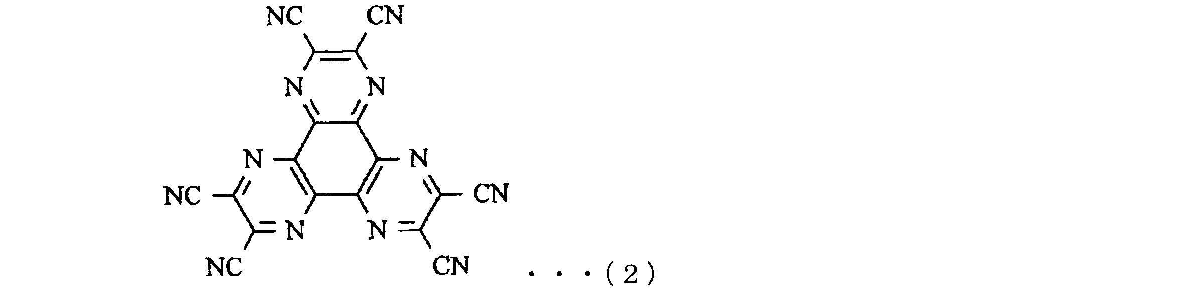
- the hole injection layer may include, for example, a hexaazatriphenylene derivative represented by the following chemical formula (2).
- the hole transport layer may contain, for example, 4,4,4-tris (3-methylphenylphenylamino) triphenylamine (m-MTDATA) or ⁇ -naphthylphenyldiamine ( ⁇ NPD).
- m-MTDATA 4,4,4-tris (3-methylphenylphenylamino) triphenylamine
- ⁇ NPD ⁇ -naphthylphenyldiamine
- the electron transport layer may contain, for example, aluminum 8-hydroxyquinoline (Alq3).
- the electron injection layer may include, for example, LiF or Li 2 O. Further, the electron injection layer may be formed as an organic compound layer doped with a donor such as an alkali metal.
- a second electrode 116G, a second electrode 116B, and a second electrode 116R having the same planar shape as that of the organic compound layer 117 (hereinafter, referred to as these If they are not distinguished from each other, they are collectively referred to as a second electrode 116). That is, the second electrode 116G is provided above the organic compound layer 117G, the second electrode 116B is provided above the organic compound layer 117B, and the second electrode 116R is provided above the organic compound layer 117R. Is provided.
- the second electrode 116 has a function of causing the organic compound layer 117 to emit light when an electric field is applied between the second electrode 116 and the first electrode 118.
- the second electrode 116 may be formed of a metal oxide.
- a transparent conductive material such as IZO, ITO, ZnO, SnO, AZO, and GZO may be used.
- the second electrode 116 is made of, for example, aluminum (Al), silver (Ag), magnesium (Mg), calcium (Ca), sodium (Na), strontium (Sr), alkali metal or alkaline earth metal and silver, It may be formed of an alloy of magnesium and silver, an alloy of magnesium and calcium, an alloy of aluminum and lithium (Li), or the like.
- a hard mask 115G, a hard mask 115B, and a hard mask 115R each having a planar shape similar to the planar shape of the second electrode 116 (hereinafter, when these are not distinguished from each other, (Also collectively referred to as a hard mask 115). That is, a hard mask 115G is provided above the second electrode 116G, a hard mask 115B is provided above the second electrode 116B, and a hard mask 115R is provided above the second electrode 116R. I have.
- the hard mask 115 functions as a mask when each sub-pixel is formed by etching.
- the film 114 is provided on the upper surface of the hard mask 115 and on each side surface of the stacked structure of the organic compound layer 117, the second electrode 116, and the hard mask 115 described above.
- the film 114 is formed of a different film for each sub-pixel.
- a uniform film 114G is provided on the side surface, the side surface of the second electrode 116G, and the side surface of the hard mask 115G.
- a part of the upper surface of the window layer 119, the upper surface of the hard mask 115B, the side surface of the organic compound layer 117B, the side surface of the second electrode 116B, and the side surface of the hard mask 115B are different from the film 114G.
- a similar film 114B is provided.
- the film 114G and the film 114B are formed on a part of the upper surface of the window layer 119, the upper surface of the hard mask 115R, the side surface of the organic compound layer 117R, the side surface of the second electrode 116R, and the side surface of the hard mask 115R.
- the film 114 is formed on the side surface of the organic compound layer 117 and the side surface of the second electrode 116, so that the organic compound layer 117 and the second electrode 116 are exposed to the air Exposure to water, oxygen, process gas, or the like can be prevented. According to this, it is possible to prevent the organic compound layer 117 and the second electrode 116 from being oxidized or the like, so that it is possible to suppress deterioration of the characteristics of the organic EL element.
- the films 114G, 114B, and 114R that are different from each other in the sub-pixel 110G, the sub-pixel 110B, and the sub-pixel 110R are provided as described above.
- the film 114G, the film 114B, and the film 114R may have different film thicknesses, for example. When the film thicknesses are different from each other, the film 114G, the film 114B, and the film 114R can be more efficiently manufactured than having the same film thickness.
- the film 114G may be the thickest
- the film 114B may be the thickest
- the film 114R may be the thinnest.
- these film thicknesses may be determined as appropriate.
- the thickness of the film 114G, the film 114B, and the film 114R may be changed in the order of forming the sub-pixels of the organic EL element.
- the organic EL element may be formed so that the film thickness increases in the order in which the sub-pixels are formed.
- the film thickness may be different depending on the film forming method. For example, in the case of using an ALD (Atomic Layer Deposition) method having a higher barrier property against oxygen or moisture, the side surface protection effect is high when the film thickness is 50 nm or less, and further when the film thickness is 10 nm or less. Even if there is, side protection effect is seen.
- ALD atomic layer Deposition
- the films 114G, 114B, and 114R may have different film qualities.
- the film quality is a property of the film that changes depending on the film forming conditions in the process of manufacturing the film.
- the deposition conditions include, for example, conditions such as a deposition method, a deposition pressure, a deposition temperature, and a deposition power. Further, as the film forming conditions, the type of the process gas, the mixing ratio, the flow rate, and the like can be cited. The density, hardness, and the like of the film change due to the difference in these film forming conditions.
- the materials of the film 114G, the film 114B, and the film 114R may be different from each other. At least one of the film 114G, the film 114B, and the film 114R may be formed of an inorganic material. Specifically, at least one or more of the films may include any one or more of AlO, TiO, SiN, SiON, and SiO among inorganic materials. By using these materials, the films 114G, 114B, and 114R can exhibit higher barrier properties against oxygen or moisture.
- At least one of the films 114G, 114B, and 114R may be formed of an organic material. Specifically, at least one of the film 114G, the film 114B, and the film 114R may be a hydrocarbon containing a fluorine atom.
- the film 114G, the film 114B, and the film 114R are not limited to a single-layer film, and may be formed by stacking a plurality of films.
- a single film 114G, a film 114B, and a film 114R may be formed by stacking different films.
- a filling layer 113 is formed above the films 114G, 114B, and 114R.
- the filling layer 113 has a function of sealing each of the organic EL elements 100 to prevent entry of moisture or the like into the organic compound layer 117. Further, the filling layer 113 also has a function of bonding an upper part of the filling layer 113 such as the opposite glass 111 described later.
- the filling layer 113 may be formed of, for example, an organic resin.
- the organic resin may be a known material such as a thermosetting resin or a UV curing resin.
- a gas barrier layer may be formed as a lower layer below the filling layer 113. While the filling layer 113 has a laminated structure formed of an organic resin, the gas barrier layer may be formed of an insulating inorganic material. The gas barrier layer has a function of enhancing gas barrier properties for the sub-pixel.
- the insulating inorganic material forming the gas barrier layer is a material that can transmit light generated in the organic compound layer 117, and is formed of a material that transmits, for example, 80% or more of the light generated in the organic compound layer 117. Is desirable.
- an inorganic amorphous insulating material can be exemplified. Since the inorganic amorphous insulating material does not generate grains, it has low water permeability and forms a good protective film.
- the insulating inorganic material forming the gas barrier layer is a transparent material, and is desirably a dense material that does not transmit moisture.
- SiNX containing amorphous silicon nitride ( ⁇ -Si 1-x N x ) and SiOy containing amorphous silicon oxide ( ⁇ -Si 1-y O y ) are used as the insulating material forming the gas barrier layer.
- a green color filter 112G, a blue color filter 112B, and a red color filter 112R are collectively referred to as a color filter 112).
- a green color filter 112G is formed in a region overlapping with the organic compound layer 117G emitting green light
- a blue color filter 112B is formed in a region overlapping with the organic compound layer 117B emitting blue light.
- a red color filter 112R is formed in a region overlapping with the organic compound layer 117G that emits light.
- the green color filter 112G, the blue color filter 112B, and the red color filter 112R adjust the color or wavelength of light emitted from the organic compound layer 117 of each sub-pixel.
- the green color filter 112G, the blue color filter 112B, and the red color filter 112R may not be provided in some cases.
- a black matrix layer BM is formed between the green color filter 112G and the blue color filter 112B and between the blue color filter 112B and the red color filter 112R.
- the black matrix layer BM can prevent light emitted from the light emitting layer from being incident on the color filter 112 of another adjacent sub-pixel and causing color mixture.
- the black matrix layer BM may be, for example, a black resin film mixed with a black colorant and having an optical density of 1 or more. Specifically, it may be a black polyimide resin. Further, the black matrix layer BM may be a thin film filter utilizing thin film interference.
- the thin film filter is formed, for example, by laminating two or more thin films made of a metal, a metal nitride, or a metal oxide, and can attenuate light using interference of the thin films.
- Specific examples of the thin film filter include a structure in which Cr and trivalent chromium oxide (Cr 2 O 3 ) are alternately laminated.
- an opposing glass 111 is formed uniformly for each sub-pixel.
- the opposing glass 111 is formed of a material that transmits light emitted from the organic compound layer 117, and is, for example, high strain point glass, soda glass (Na 2 O.CaO.SiO 2 ), or borosilicate glass (Na 2 O). ⁇ B 2 O 3 ⁇ SiO 2 ), lead glass (Na 2 O) various glass substrates such as may be a quartz substrate, or the like.
- FIGS. 2 to 18 are views showing an example of a manufacturing process of the organic EL element 100.
- a substrate 120 that supports a stacked structure of the organic EL element 100 and includes a driving circuit such as a driving transistor for driving the organic EL element 100 is formed.
- the first electrode 118 and the window layer 119 are formed on the substrate 120 by using a sputtering method, CVD (Chemical Vapor Deposition), or ALD (Atomic Layer Deposition).
- a metal layer made of ITO is formed as a first electrode 118 on a substrate 120 on which a circuit layer including a driving circuit is formed on a Si substrate, and the metal layer is formed using a photolithography technique and an etching technique. Is patterned. Thereafter, an insulating layer is formed as a window layer 119 so as to fill a region separating each sub-pixel between the patterned metal layers.
- the window layer 119 may be specifically formed of SiON or the like.
- an organic compound layer 117G is formed on the first electrode 118 and the window layer 119 by a coating method such as a vacuum deposition method, a spin coating method, and a die coating method.
- a coating method such as a vacuum deposition method, a spin coating method, and a die coating method.
- a second electrode 116G and a hard mask 115G are further formed.
- the organic compound layer 117G may be formed with the above-described laminated structure and material.
- the second electrode 116G may be formed of a material including IZO
- the hard mask 115G may be formed of a material including SiN.
- the hard mask 115G may be formed of a CVD film containing SiO, SiON, or the like, or an ALD film containing AlO, TiO, SiO, or the like.
- the second electrode 116G is not limited to IZO, but may be another metal oxide such as ITO, or a metal electrode such as an MgAg alloy, Al, or Ca. Further, the hard mask 115G does not necessarily have to be formed.
- a resist 131G having a plane shape similar to the plane shape of the first electrode 118G is formed on a desired position of the hard mask 115G by photolithography.
- the resist 131G functions as a mask when etching the hard mask 115G.
- the hard mask 115G is patterned.
- the etching of the hard mask 115G may be performed by plasma etching using a fluorine-based hydrocarbon gas.
- the resist 131G on the protected hard mask 115G is removed.
- the removal of the resist 131G is performed by ashing.
- the removal of the resist may be performed after the step of etching the second electrode 116G and the organic compound layer 117G shown in FIG. 7 described below.
- a film 114 ⁇ / b> G is formed on the stacked structure of the sub-pixels in the green light emitting region G. Specifically, the film 114G is formed uniformly over the entire surface of the substrate 120 including the green light emitting region G.
- the film 114G may be formed of AlO using, for example, an ALD method.
- the film 114G is not limited to AlO, but may be another ALD film such as TiO, or a CVD film such as SiN, SiO, or SiON.
- damage such as deterioration of the organic compound layer 117G in the subsequent steps can be suppressed.
- it is possible to suppress deterioration of the organic compound layer 117G due to contact of a side surface of the organic compound layer 117G with a process gas used in forming another sub-pixel, water or oxygen in the air, or the like. Can be.
- the film 114G in a region other than the green light emitting region G is removed by etching. Specifically, a resist is formed above each component of the green light emitting region G, and the film 114G is etched using the resist as a mask. Thereby, the film 114G in the region other than the green light emitting region G is removed. Note that the film 114G can be etched using a chlorine-based gas. The resist is removed by ashing.
- the formation of the green-emitting sub-pixel 110G including the film 114G is completed. Subsequently, the formation of the sub-pixel 110B in the blue light-emitting region B is performed in the same manner as the formation of the sub-pixel 110G that emits green light. The manufacture of the sub-pixel 110B that emits blue light will be described with reference to FIGS.
- an organic compound layer 117B that emits blue light, a second electrode 116B, and a hard mask 115B are formed over the entire surface of the substrate 120 in the same manner as when the sub-pixel 110G that emits green light is formed. .
- a resist 131B having a plane shape similar to the plane shape of the first electrode 118B is formed on a desired position of the hard mask 115B by photolithography.
- the resist 131B functions as a mask when etching the hard mask 115B.
- the hard mask 115B is etched by using the resist 131B as a mask.
- the second electrode 116B and the organic compound layer 117B are patterned by etching using the hard mask 115B as a mask. Note that the resist 131B may be removed by ashing or the like.
- the etching of the hard mask 115B may be performed by, for example, plasma etching using a fluorine-based hydrocarbon gas, as in the process of forming the sub-pixel 110G in the green light emitting region G.
- the etching of the second electrode 116B formed of IZO may be performed by dry etching using argon, and the etching of the organic compound layer 117B may be performed by dry etching using oxygen.
- the film 114G covering the side surface of the organic compound layer 117G prevents the organic compound layer 117G from being exposed to a process gas during these etching, and prevents the organic compound layer 117G from being exposed to a process gas. Exposure to the water or oxygen in it can be prevented. Thus, the film 114G can suppress deterioration of the organic compound layer 117G.
- the side surface of the second electrode 116G is also covered with the film 114G, the second electrode 116G must be protected from damage due to the steps including the etching and contact with moisture or oxygen in the air. Can be.
- the film 114B is formed by the green light emitting region G, the blue light emitting region B, and the red light emitting region R ( That is, it is formed uniformly over the entire surface of the substrate 120).
- the film 114B may be formed by the same method as when the film 114G is formed.
- the film 114B may be formed of the same material (for example, AlO) as the film 114G by using, for example, an ALD method. At this time, in the film 114G, AlO when the film 114B is formed is further overlapped, so that the film 114G has a greater thickness. Therefore, the film 114G is formed to be thicker than the film 114B.
- the film 114G and the film 114B may be formed to have different thicknesses, or may be formed to have different film qualities or materials and have the same thickness.
- the film 114G and the film 114B are formed to have the same thickness
- the film 114G formed to be thicker than the film 114B is removed by etching or the like until the film 114G has a thickness equivalent to the film 114B, so that the film thickness is the same.
- the film 114G and the film 114B can be formed.
- the film 114B may be formed of a material different from the material forming the film 114G immediately above the hard mask 115G.
- the film 114G immediately above the hard mask 115G is formed of AlO and the film 114B is formed of a material different from AlO
- the film 114G is formed of a layer formed of AlO and a layer formed of another material. As a laminated film.
- a resist is formed on the films 114G and 114B in the green light emitting region G and the blue light emitting region B, and dry etching or the like is performed using the resist as a mask to remove the film 114B in the red light emitting region R. can do.
- the formation of the sub-pixel 110B that emits blue light is completed. Subsequently, similarly to the formation of the sub-pixel 110G that emits green light and the sub-pixel 110B that emits blue light, the formation of the sub-pixel 110R that emits red light is performed. The manufacture of the sub-pixel 110R that emits red light will be described with reference to FIGS.
- a resist 131R having a planar shape similar to the planar shape of the first electrode 118R is formed on a desired position of the hard mask 115R by photolithography.
- the resist 131R functions as a mask when etching the hard mask 115R.
- the resist 131R is masked in the step of forming the sub-pixel 110R that emits red light, as in the step of forming the sub-pixel 110G that emits green light and the sub-pixel 110B that emits blue light.
- the hard mask 115R is patterned by the etching described above, and the second electrode 116R and the organic compound layer 117R are patterned by the etching using the hard mask 115R as a mask. Note that the resist 131R may be removed by ashing or the like.
- the film 114G and the film 114B cover the side surfaces of the organic compound layer 117G and the organic compound layer 117B. Therefore, the film 114G and the film 114B cause damage to the organic compound layer 117G and the organic compound layer 117B due to the etching process and moisture in the air during the etching for forming the sub-pixel 110R in the red light emitting region R. Alternatively, contact with oxygen can be suppressed. Thus, the 114G and the film 114B can suppress deterioration of the organic compound layer 117G and the organic compound layer 117B.
- the film 114R may be formed of the same material (for example, AlO) as the film 114G and the film 114B by using, for example, the ALD method.
- AlO when the film 114R is formed is further overlapped, so that the thickness of the film 114G is further increased. Therefore, in the film 114G, the film 114B, and the film 114R, the film 114G is formed. Is the thickest, then the film 114B is the thickest, and the film 114R is the thinnest.
- the film thickness of the film 114G, the film 114B, and the film 114R may be formed differently between the sub-pixels emitting light of different colors in this manner, and the film quality or material is different and the film thickness is the same. May be formed.
- the film 114G, the film 114B, and the film 114R are formed to have the same thickness, for example, the film 114G and the film 114B which are formed to be thicker than the film 114R are etched until the film 114R corresponds to the thickness of the film 114R. By removal, the films 114G, 114B, and 114R having the same thickness can be formed.
- the film 114R may be formed of the same material and different film qualities as the film 114G and the film 114B.
- Factors affecting the film quality include film forming conditions such as a film forming method, a film forming pressure, a film forming temperature, or a film forming power, a type of process gas, a mixing ratio, or a flow rate. Examples include film density and film hardness.
- the film 114R may be formed under different film formation conditions from those of the film 114G and the film 114B.
- a filling layer 113 commonly used between the sub-pixels is formed.
- the filling layer 113 may be at least formed of an organic resin that protects the entire surface of the stacked structure of each sub-pixel. According to this, the filling layer 113 influences the external structure on the stacked structure of the organic EL element 100 sealed by the filling layer 113, specifically, damage due to a process gas at the time of manufacturing, and moisture or oxygen in the atmosphere. Contact can be suppressed.
- a gas barrier layer that covers each sub-pixel in common may be formed on the film 114.
- the gas barrier layer may be formed by a film forming method such as a CVD method, a MOCVD (Metal Organic Chemical Vapor Deposition) method, and an ALD method.
- the gas barrier layer is set at a film formation temperature of 150 ° C. or less in order to prevent a decrease in luminance due to the deterioration of the organic compound layer 117, and further, to prevent the gas barrier layer from peeling off. Is desirably formed under the condition in which is minimized.
- a color filter may be formed using an OCCF (On Chip Color Filter) method in which a color resist is formed by photolithography on the film 114 or the gas barrier layer before the formation of the filling layer. In some cases, a color filter may not be provided.
- OCCF On Chip Color Filter
- the thickness, quality, and material of the film 114 formed on the side surface of the organic compound layer 117 may be appropriately determined as long as at least one of the characteristics is different from each other, and is not limited to such an example.
- the film 114 may be formed by each combination.
- the sub-pixels are manufactured in the order of the green light emitting region G, the blue light emitting region B, and the red light emitting region R, but the manufacturing order of the sub pixels is not limited to this example.
- FIG. 19 is a diagram illustrating an example (Modification 1) of a modification of the organic EL element according to the present embodiment.
- the color filter, the black matrix, and the opposing glass are not shown and are omitted.
- films 214G, 214B, and 214R are formed only on both side surfaces of the sub-pixel 210G, the sub-pixel 210B, and the sub-pixel 210R.
- the films 214G, 214B, and 214R are formed only on the side surfaces of the sub-pixel 210G including the side surfaces of the organic compound layer 217G, the organic compound layer 217B, and the organic compound layer 217R, and the sub-pixels 210B and 210R. Is formed. That is, the film 214 is not formed above each sub-pixel 210, specifically, above the hard mask 215.
- the organic EL element 200 differs from the organic EL element 100 in this point.
- the film 214G, the film 214B, and the film 214R in the first modification are formed simultaneously with the dry etching of the organic compound layer 217 by dry-etching the organic compound layer 217 as described below in the above-described manufacturing process.
- a gas having a relatively high carbon ratio such as C 4 F 8
- an organic material as an etching deposit specifically, a carbon atom containing fluorine atoms is formed on the side surface of the organic compound layer 217.
- the film 214 can be formed by forming a hydrogen-based CF polymer or the like.
- the film 214 is formed of a different material depending on the type of gas used or the material to be etched. The material of the film 214 may be determined as appropriate.
- the film 214G, the film 214B, and the film 214R shown in the first modification may be formed simultaneously with the dry etching as described above, but may be formed by applying a sidewall formation technique.
- the sidewall technology is applied, after the organic compound layer 217 is dry-etched, the film 214 is formed so as to bury the configuration of each sub-pixel in each sub-pixel, and the film 214 is subjected to anisotropic etching.
- the film 214 can be left only on the side surface of the organic compound layer 217.
- the organic compound layer 217 can be covered with the film 214.
- the step of patterning the film 214 using a resist can be reduced.
- FIG. 20 is a diagram illustrating an example (Modification 2) of a modification of the organic EL element according to the present embodiment.
- the filling layer, the color filter, the black matrix, and the facing glass are not shown and are omitted.
- the organic EL element 300 unlike the organic EL element 100 shown in FIG. 1, for the sub-pixel 310R that emits red light, the film 314G formed in the sub-pixel 310G that emits green light and the sub-pixel 310B that emits blue light and A film that covers the side surface corresponding to the film 314B is not formed.
- the side surface of the sub-pixel 310R is covered with a protective film 314R that is formed in common over the sub-pixel 310G, the sub-pixel 310B, and the sub-pixel 310R.
- the protective film 314R may be a gas barrier layer, and after forming the protective film 314R, a filling layer may be formed on the protective film 314R.
- the organic compound layer 317R is exposed to the etching process gas without performing a step of dry-etching the organic compound layer of another sub-pixel after forming the sub-pixel 310R. None be.
- FIG. 21 is a view showing an example (Modification 3) of a modification of the organic EL element according to the present embodiment.
- the filling layer, the color filter, the black matrix, and the opposing glass are not shown and are omitted.
- a common electrode 416 provided continuously over the sub-pixels 410G, 410B, and 410R having different emission colors is formed. . That is, in the organic EL element 400 shown in FIG. 21, the second electrode 316G and the second electrode 316G in each sub-pixel laminated on the organic compound layer 317G, the organic compound layer 317B, and the organic compound layer 317R as shown in FIG.
- FIG. 22 is a diagram illustrating an example (Modification 4) of a modification of the organic EL element according to the present embodiment.
- the color filter, the black matrix, and the opposing glass are not shown and are omitted.
- the hard mask 115 is not formed.
- the films 514G, 514B are formed on the second electrode 516G, the second electrode 516B, and the second electrode 516R with respect to the sub-pixels 510G, 510B, and 510R. And a film 514R. This also prevents the organic compound layer 517G, the organic compound layer 517B, and the organic compound layer 517G from being exposed to a gas such as air or a process gas by the films 514G, 514B, and 514R.
- FIGS. 23 to 26 are diagrams showing an example of a planar layout of sub-pixels.
- FIGS. 23 to 26 each represent a pixel opening, and G, B, and R described in each rectangle represent a sub-pixel G that emits green, a sub-pixel B that emits blue, and a red that emits red, respectively.
- FIG. The dashed line indicates a portion where the organic compound layer is divided.
- sub-pixel G, sub-pixel B, and sub-pixel R are arranged in order in the first direction (horizontal direction opposite to FIG. 23) at equal intervals.
- the sub-pixel G, the sub-pixel B, and the sub-pixel R are separated from each other, and the organic compound layer is separated in each of the sub-pixels.
- sub-pixels of the same color as each sub-pixel are arranged separately, and the organic compound layer is divided in each sub-pixel. ing.
- Each sub-pixel may be arranged in such a layout.
- the sub-pixel B may have a smaller amount of light per unit area than the sub-pixel G and the sub-pixel R, the light amount of the entire sub-pixel can be reduced by enlarging the pixel area. May be substantially the same as the respective light amounts.
- sub-pixels R and G are sequentially arranged in the second direction (vertical direction as opposed to FIG. 24).
- a first direction horizontal direction opposite to FIG. 24
- Sub-pixels B are arranged side by side.
- the sub-pixel R, the sub-pixel G, and the sub-pixel B are repeatedly arranged.
- the sub-pixel R, the sub-pixel G, and the sub-pixel B are repeatedly arranged in the second direction.
- Each sub-pixel is separated from each other, and the organic compound layer is separated in each sub-pixel.
- Each sub-pixel may be arranged in such a layout.
- sub-pixel G, sub-pixel B, and sub-pixel R are sequentially arranged at equal intervals in the first direction (horizontal direction as opposed to FIG. 25).
- the sub-pixel G, the sub-pixel B, and the sub-pixel R are separated from each other, and the organic compound layer is separated in each of the sub-pixels.
- the sub-pixels of the same color as the respective sub-pixels are arranged separately from each other, but emit the same color.
- the organic compound layer is not divided between the sub-pixels.
- each of the sub-pixels can be independently driven by forming the first electrode 118 or the second electrode 116 in each of the sub-pixels where the organic compound layer is continuous. According to this, since the patterning of the organic compound layer can be simplified, the organic EL element 100 can be manufactured more easily.
- sub-pixels R and G are sequentially arranged in the second direction (vertical direction opposite to FIG. 26).
- a first direction horizontal direction opposite to FIG. 26
- a length equal to the total length of the sub-pixels R and G in the second direction is set.
- Sub-pixels B are arranged side by side.
- the sub-pixel R, the sub-pixel G, and the sub-pixel B are repeatedly arranged.
- the sub-pixel R, the sub-pixel G, and the sub-pixel B are repeatedly arranged in the second direction.
- the organic compound layer is not divided between the sub-pixels of the same color.
- an organic compound layer may be continuously provided in a plurality of subpixels of the same color. Even in such a case, each of the sub-pixels can be driven independently by forming the first electrode 118 or the second electrode 116 in each of the sub-pixels where the organic compound layer is continuous. According to this arrangement example, the minimum processing dimension of the organic compound layer can be made larger, so that the tolerance of the dimension error of the organic compound layer can be relaxed during patterning, and the organic compound layer can be formed with a simpler processing technique.
- the layers can be processed.
- each sub-pixel to which the present disclosure can be applied may be, for example, a long side of a rectangle of the sub-pixel of 100 ⁇ m or less, or a finer 10 ⁇ m or less.
- each sub-pixel is rectangular.
- the present invention is not limited to this example, and each sub-pixel may have various planar shapes.
- the plane size may be, for example, the size of a long side if it is a triangle, or the diameter or the like of a circumscribed circle of the polygon if it is a pentagon or more polygon.
- the plane size may be a diameter if it is a circular shape, and may be a long diameter if it is an elliptical shape. The technique of the present disclosure can be particularly effectively applied when fine processing such as forming a sub-pixel having such a plane size is required.
- the following configuration also belongs to the technical scope of the present disclosure.
- At least two or more sub-pixels in which the first electrode and the second electrode are stacked with an organic compound layer including at least a light-emitting layer emitting different colors interposed therebetween on a plane orthogonal to the stacking direction Provided, The side surface of the organic compound layer is covered with a different film for each of the sub-pixels, Organic EL element.
- the sub-pixel is formed by stacking the first electrode, the organic compound layer, and the second electrode in this order, A film different for each sub-pixel covering a side surface of the organic compound layer, further covering a side surface of the second electrode; The organic EL device according to any one of the above (1) to (6).
- the second electrode stacked on the organic compound layer is connected to the second electrode of the adjacent sub-pixel, or On the second electrode laminated on the organic compound layer, a common electrode continuously provided on the second electrode of the adjacent sub-pixel is further provided.
- the organic EL device according to (8), wherein the second electrode or the common electrode transmits part of light and reflects part of light.
- the organic EL device according to (7), wherein the second electrode is a cathode.
- the organic EL device according to (7), wherein the second electrode is formed of a metal oxide.
- (12) The organic EL device according to any one of (1) to (11), wherein a plane size of the sub-pixel is 100 ⁇ m or less.
Landscapes
- Engineering & Computer Science (AREA)
- Manufacturing & Machinery (AREA)
- Microelectronics & Electronic Packaging (AREA)
- Physics & Mathematics (AREA)
- Optics & Photonics (AREA)
- General Physics & Mathematics (AREA)
- Theoretical Computer Science (AREA)
- Electroluminescent Light Sources (AREA)
Abstract
Description
なお、上記の効果は必ずしも限定的なものではなく、上記の効果とともに、または上記の効果に代えて、本明細書に示されたいずれかの効果、または本明細書から把握され得る他の効果が奏されてもよい。
1.有機EL素子の概要
2.有機EL素子の構成
3.有機EL素子の製造方法
4.変形例
5.有機EL素子の平面レイアウト
まず、本開示の一実施形態にかかる有機EL素子の概要を説明する。本開示の有機EL素子では、それぞれ異なる色が発光される発光層を少なくとも含む有機化合物層が設けられている。さらに、その有機化合物層を挟んで第1電極および第2電極が積層されている。この構成を有する副画素が、積層方向と直交する平面上に互いに離隔して少なくとも2つ以上設けられる。
図1を参照して、本開示の一実施形態に係る有機EL素子の構成について説明する。図1は、本開示の一実施形態に係る有機EL素子を積層方向に切断した断面を模式的に示す断面図である。

以上までで、有機EL素子の構造を説明した。次に、図2~図18を参照して、図1に示した有機EL素子100の製造方法に関して説明を行う。図2~図18は、有機EL素子100の製造工程の一例を示した図である。
以上までで、図1に示した有機EL素子の製造方法に関して説明した。本開示の技術では、有機化合物層117に対して有機EL素子の製造時のプロセスによるダメージ、および大気中の水分または酸素への接触による有機化合物層の劣化が発生しないように、有機化合物層117の側面に膜114を形成する。膜114により有機化合物層117の側面を保護する構造として、以下では、図1の変形例の一例を図19~図22を参照して説明する。図1と同様の構造は、説明を省略し、図1と異なる点に関して説明を行う。
図19は、本実施形態にかかる有機EL素子の変形例の一例(変形例1)を示した図である。図19では、カラーフィルタ、ブラックマトリクス、および対向ガラスは図示されておらず、省略されている。有機EL素子200では、図1に示す有機EL素子100と異なり、副画素210G、副画素210Bおよび副画素210Rの両側面にのみ膜214G、膜214B、および214Rが形成されている。具体的には、有機化合物層217G、有機化合物層217B、および有機化合物層217Rの側面を含む副画素210G、副画素210Bおよび副画素210Rの互いに隣接する側面にのみ膜214G、膜214B、および214Rが形成されている。つまり、各副画素210における上部、具体的にはハードマスク215の上部には、膜214が形成されていない。有機EL素子200では、この点が、有機EL素子100と異なる。
図20は、本実施形態にかかる有機EL素子の変形例の一例(変形例2)を示した図である。図20では、充填層、カラーフィルタ、ブラックマトリクス、および対向ガラスは図示されておらず、省略されている。有機EL素子300では、図1に示す有機EL素子100と異なり、赤色を発光する副画素310Rに対して、緑色を発光する副画素310Gおよび青色を発光する副画素310Bに形成される膜314Gおよび膜314Bに対応する側面を覆う膜が形成されていない。そのかわり、副画素310Rは、副画素310G、副画素310Bおよび副画素310Rに亘って共通して形成される保護膜314Rにて側面が覆われている。保護膜314Rは、具体的には、ガスバリア層であってよく、保護膜314Rの形成後には、保護膜314Rの上層に充填層が形成されてもよい。例えば、副画素310Rは、最後に形成されるため、副画素310Rを形成した後に他の副画素の有機化合物層をドライエッチングする工程を経ることがなく、有機化合物層317Rがエッチングプロセスガスに曝されることがない。また、保護膜314Rが形成されることにより、大気中の水または酸素等と有機化合物層との接触を防ぐことができることは言うまでもない。したがって、保護膜314Rにより、有機EL素子300では、有機化合物層の劣化を抑制することができる。
図21は、本実施形態にかかる有機EL素子の変形例の一例(変形例3)を示した図である。図21では、充填層、カラーフィルタ、ブラックマトリクス、および対向ガラスは図示されておらず、省略されている。有機EL素子400では、図20に示す有機EL素子300とさらに異なり、発光色の異なる副画素410G、副画素410Bおよび副画素410Rに亘って連続して設けられた共通電極416が形成されている。つまり、図21に示す有機EL素子400では、図20に示すような有機化合物層317G、有機化合物層317Bおよび有機化合物層317Rの上に積層された各副画素における第2電極316G、第2電極316B、第2電極316R、がそれぞれ互いに隣接する副画素の第2電極316G、第2電極316B、第2電極316Rと電気的に接続されている。図21では、図20では各副画素に個別に配置されていた第2電極316が互いに連結されることで、共通電極416として形成されている。
図22は、本実施形態にかかる有機EL素子の変形例の一例(変形例4)を示した図である。図22では、カラーフィルタ、ブラックマトリクス、および対向ガラスは図示されておらず、省略されている。有機EL素子500では、図1に示す有機EL素子100と異なり、ハードマスク115が形成されていない。具体的には、有機EL素子500では、副画素510G、副画素510Bおよび副画素510Rに対して、第2電極516G、第2電極516B、および第2電極516Rの上に、膜514G、膜514Bおよび膜514Rが形成されている。これによっても有機化合物層517G、有機化合物層517B、および有機化合物層517Gは、膜514G、膜514Bおよび膜514Rによって、大気等のガスまたはプロセスガスに曝されることを防止している。
以上までで、本実施形態に係る有機EL素子の構造の変形例の一例を説明した。次に、図1に示したような副画素の平面での配置例の一例を図23~図26を参照して説明する。図23~図26は、副画素の平面配置レイアウトの一例を示した図である。
(1)
それぞれ異なる色が発光される発光層を少なくとも含む有機化合物層を挟んで第1電極および第2電極が積層される副画素が、前記積層方向と直交する平面上に互いに離隔して少なくとも2つ以上設けられ、
前記有機化合物層の側面は、前記副画素毎に異なる膜で覆われる、
有機EL素子。
(2)
前記膜は、前記副画素毎に膜厚、膜質、または膜材料の少なくともいずれか一つ以上が異なる、前記(1)に記載の有機EL素子。
(3)
前記膜の少なくとも1つ以上は、無機系材料で形成される、前記(1)または前記(2)に記載の有機EL素子。
(4)
前記膜の少なくとも1つ以上は、AlO、TiO、SiN、SiON、又はSiOのいずれか1つ以上を含む、前記(3)に記載の有機EL素子。
(5)
前記膜の少なくとも1つ以上は、有機系材料で形成される、前記(1)または前記(2)に記載の有機EL素子。
(6)
前記有機系材料は、フッ素原子を含む炭化水素である、前記(5)に記載の有機EL素子。
(7)
前記副画素は、前記第1電極、前記有機化合物層、および前記第2電極の順に積層されることで形成され、
前記有機化合物層の側面を覆う前記副画素毎に異なる膜は、前記第2電極の側面をさらに覆う、
前記(1)~前記(6)のいずれか一項に記載の有機EL素子。
(8)
前記有機化合物層の上に積層された前記第2電極は、隣接する前記副画素の前記第2電極と接続される、または、
前記有機化合物層の上に積層された前記第2電極の上には、隣接する前記副画素の前記第2電極の上に連続して設けられる共通電極が更に設けられる、
前記(7)に記載の有機EL素子。
(9)
前記第2電極または前記共通電極は、光の一部を透過し、光の一部を反射する、前記(8)に記載の有機EL素子。
(10)
前記第2電極は、カソードである、前記(7)に記載の有機EL素子。
(11)
前記第2電極は金属酸化物で形成される、前記(7)に記載の有機EL素子。
(12)
前記副画素の平面サイズは、100μm以下である、前記(1)~前記(11)のいずれか一項に記載の有機EL素子。
(13)
前記副画素の平面サイズは、10μm以下である、前記(1)~前記(11)のいずれか一項に記載の有機EL素子。
(14)
それぞれ異なる色が発光される発光層を少なくとも含む有機化合物層を挟んで第1電極および第2電極が積層される副画素を前記積層方向と直交する平面上に互いに離隔して少なくとも2つ以上形成すること、を含み、
前記副画素の形成では、前記有機化合物層の側面を覆う膜を形成することを、各色を発光する前記有機化合物層を形状加工する都度行う、
有機EL素子の製造方法。
111 対向ガラス
112 カラーフィルタ
113 充填層
114 膜
115 ハードマスク
116 第2電極
117 有機化合物層
118 第1電極
119 Window層
120 基板
131G、131B、131R レジスト
Claims (14)
- それぞれ異なる色が発光される発光層を少なくとも含む有機化合物層を挟んで第1電極および第2電極が積層される副画素が、前記積層方向と直交する平面上に互いに離隔して少なくとも2つ以上設けられ、
前記有機化合物層の側面は、前記副画素毎に異なる膜で覆われる、
有機EL素子。 - 前記膜は、前記副画素毎に膜厚、膜質、または膜材料の少なくともいずれか一つ以上が異なる、請求項1に記載の有機EL素子。
- 前記膜の少なくとも1つ以上は、無機系材料で形成される、請求項1に記載の有機EL素子。
- 前記膜の少なくとも1つ以上は、AlO、TiO、SiN、SiON、又はSiOのいずれか1つ以上を含む、請求項3に記載の有機EL素子。
- 前記膜の少なくとも1つ以上は、有機系材料で形成される、請求項1に記載の有機EL素子。
- 前記有機系材料は、フッ素原子を含む炭化水素である、請求項5に記載の有機EL素子。
- 前記副画素は、前記第1電極、前記有機化合物層、および前記第2電極の順に積層されることで形成され、
前記有機化合物層の側面を覆う前記副画素毎に異なる膜は、前記第2電極の側面をさらに覆う、
請求項1に記載の有機EL素子。 - 前記有機化合物層の上に積層された前記第2電極は、隣接する前記副画素の前記第2電極と接続される、または、
前記有機化合物層の上に積層された前記第2電極の上には、隣接する前記副画素の前記第2電極の上に連続して設けられる共通電極が更に設けられる、
請求項7に記載の有機EL素子。 - 前記第2電極または前記共通電極は、光の一部を透過し、光の一部を反射する、請求項8に記載の有機EL素子。
- 前記第2電極は、カソードである、請求項7に記載の有機EL素子。
- 前記第2電極は金属酸化物で形成される、請求項7に記載の有機EL素子。
- 前記副画素の平面サイズは、100μm以下である、請求項1に記載の有機EL素子。
- 前記副画素の平面サイズは、10μm以下である、請求項1に記載の有機EL素子。
- それぞれ異なる色が発光される発光層を少なくとも含む有機化合物層を挟んで第1電極および第2電極が積層される副画素を前記積層方向と直交する平面上に互いに離隔して少なくとも2つ以上形成すること、を含み、
前記副画素の形成では、前記有機化合物層の側面を覆う膜を形成することを、各色を発光する前記有機化合物層を形状加工する都度行う、
有機EL素子の製造方法。
Priority Applications (6)
| Application Number | Priority Date | Filing Date | Title |
|---|---|---|---|
| JP2020527402A JP7394758B2 (ja) | 2018-06-25 | 2019-06-14 | 有機el素子および有機el素子の製造方法 |
| US17/252,795 US11678550B2 (en) | 2018-06-25 | 2019-06-14 | Organic EL device and method for manufacturing organic EL devices |
| CN202510156290.7A CN120051118A (zh) | 2018-06-25 | 2019-06-14 | 有机el器件 |
| CN201980040795.XA CN112314056B (zh) | 2018-06-25 | 2019-06-14 | 有机el器件和用于制造有机el器件的方法 |
| US18/311,485 US12096671B2 (en) | 2018-06-25 | 2023-05-03 | Organic EL device and method for manufacturing organic EL devices |
| US18/805,397 US20250008802A1 (en) | 2018-06-25 | 2024-08-14 | Organic el device and method for manufacturing organic el devices |
Applications Claiming Priority (2)
| Application Number | Priority Date | Filing Date | Title |
|---|---|---|---|
| JP2018119504 | 2018-06-25 | ||
| JP2018-119504 | 2018-06-25 |
Related Child Applications (2)
| Application Number | Title | Priority Date | Filing Date |
|---|---|---|---|
| US17/252,795 A-371-Of-International US11678550B2 (en) | 2018-06-25 | 2019-06-14 | Organic EL device and method for manufacturing organic EL devices |
| US18/311,485 Continuation US12096671B2 (en) | 2018-06-25 | 2023-05-03 | Organic EL device and method for manufacturing organic EL devices |
Publications (1)
| Publication Number | Publication Date |
|---|---|
| WO2020004086A1 true WO2020004086A1 (ja) | 2020-01-02 |
Family
ID=68984825
Family Applications (1)
| Application Number | Title | Priority Date | Filing Date |
|---|---|---|---|
| PCT/JP2019/023742 Ceased WO2020004086A1 (ja) | 2018-06-25 | 2019-06-14 | 有機el素子および有機el素子の製造方法 |
Country Status (4)
| Country | Link |
|---|---|
| US (3) | US11678550B2 (ja) |
| JP (1) | JP7394758B2 (ja) |
| CN (2) | CN120051118A (ja) |
| WO (1) | WO2020004086A1 (ja) |
Cited By (62)
| Publication number | Priority date | Publication date | Assignee | Title |
|---|---|---|---|---|
| JPWO2022123382A1 (ja) * | 2020-12-07 | 2022-06-16 | ||
| JP2022089790A (ja) * | 2020-12-04 | 2022-06-16 | 株式会社半導体エネルギー研究所 | 表示パネル、情報処理装置、表示パネルの製造方法 |
| WO2022130108A1 (ja) * | 2020-12-18 | 2022-06-23 | 株式会社半導体エネルギー研究所 | 表示装置および表示装置の作製方法 |
| JPWO2022144661A1 (ja) * | 2020-12-29 | 2022-07-07 | ||
| JP2022104825A (ja) * | 2020-12-29 | 2022-07-11 | 株式会社半導体エネルギー研究所 | 発光デバイス、発光装置、電子機器、および照明装置 |
| JPWO2022153150A1 (ja) * | 2021-01-14 | 2022-07-21 | ||
| JPWO2022153144A1 (ja) * | 2021-01-14 | 2022-07-21 | ||
| JPWO2022157595A1 (ja) * | 2021-01-22 | 2022-07-28 | ||
| JPWO2022172130A1 (ja) * | 2021-02-12 | 2022-08-18 | ||
| JPWO2022172116A1 (ja) * | 2021-02-12 | 2022-08-18 | ||
| WO2022172125A1 (ja) * | 2021-02-12 | 2022-08-18 | 株式会社半導体エネルギー研究所 | 発光デバイス、発光装置、電子機器および照明装置 |
| WO2022172119A1 (ja) * | 2021-02-12 | 2022-08-18 | 株式会社半導体エネルギー研究所 | 発光デバイス、発光装置、電子機器および照明装置 |
| JPWO2022172129A1 (ja) * | 2021-02-12 | 2022-08-18 | ||
| JPWO2022180468A1 (ja) * | 2021-02-25 | 2022-09-01 | ||
| JPWO2022185149A1 (ja) * | 2021-03-05 | 2022-09-09 | ||
| JPWO2022185150A1 (ja) * | 2021-03-05 | 2022-09-09 | ||
| JPWO2022189916A1 (ja) * | 2021-03-11 | 2022-09-15 | ||
| WO2022200916A1 (ja) * | 2021-03-25 | 2022-09-29 | 株式会社半導体エネルギー研究所 | 表示装置、表示装置の作製方法、表示モジュール、及び電子機器 |
| WO2022214916A1 (ja) * | 2021-04-08 | 2022-10-13 | 株式会社半導体エネルギー研究所 | 表示装置、表示装置の作製方法、表示モジュール、電子機器 |
| JPWO2022214904A1 (ja) * | 2021-04-08 | 2022-10-13 | ||
| JPWO2022224080A1 (ja) * | 2021-04-23 | 2022-10-27 | ||
| WO2022248962A1 (ja) * | 2021-05-27 | 2022-12-01 | 株式会社半導体エネルギー研究所 | 表示装置、表示モジュール、及び、電子機器 |
| JPWO2022259077A1 (ja) * | 2021-06-08 | 2022-12-15 | ||
| JPWO2022259068A1 (ja) * | 2021-06-08 | 2022-12-15 | ||
| WO2022263964A1 (ja) * | 2021-06-17 | 2022-12-22 | 株式会社半導体エネルギー研究所 | 表示装置 |
| WO2023275660A1 (ja) * | 2021-06-30 | 2023-01-05 | 株式会社半導体エネルギー研究所 | 表示装置、及び表示装置の作製方法 |
| WO2023285907A1 (ja) * | 2021-07-16 | 2023-01-19 | 株式会社半導体エネルギー研究所 | 表示装置、表示モジュール、電子機器、及び、表示装置の作製方法 |
| JPWO2023285906A1 (ja) * | 2021-07-16 | 2023-01-19 | ||
| JPWO2023002279A1 (ja) * | 2021-07-21 | 2023-01-26 | ||
| WO2023002297A1 (ja) * | 2021-07-21 | 2023-01-26 | 株式会社半導体エネルギー研究所 | 表示装置、及び表示装置の作製方法 |
| WO2023012565A1 (ja) * | 2021-08-05 | 2023-02-09 | 株式会社半導体エネルギー研究所 | 表示装置、表示モジュール、電子機器、及び、表示装置の作製方法 |
| JPWO2023012576A1 (ja) * | 2021-08-05 | 2023-02-09 | ||
| WO2023012564A1 (ja) * | 2021-08-05 | 2023-02-09 | 株式会社半導体エネルギー研究所 | 表示装置、表示モジュール、電子機器、及び、表示装置の作製方法 |
| WO2023017357A1 (ja) * | 2021-08-12 | 2023-02-16 | 株式会社半導体エネルギー研究所 | 表示装置 |
| WO2023021365A1 (ja) * | 2021-08-19 | 2023-02-23 | 株式会社半導体エネルギー研究所 | 表示装置の作製方法、表示装置、表示モジュール、及び、電子機器 |
| JPWO2023026126A1 (ja) * | 2021-08-26 | 2023-03-02 | ||
| WO2023026128A1 (ja) * | 2021-08-27 | 2023-03-02 | 株式会社半導体エネルギー研究所 | 表示装置 |
| WO2023047249A1 (ja) * | 2021-09-24 | 2023-03-30 | 株式会社半導体エネルギー研究所 | 表示装置、表示モジュールおよび電子機器 |
| WO2023047235A1 (ja) * | 2021-09-24 | 2023-03-30 | 株式会社半導体エネルギー研究所 | 表示装置の作製方法 |
| WO2023052907A1 (ja) * | 2021-09-30 | 2023-04-06 | 株式会社半導体エネルギー研究所 | 表示装置 |
| WO2023057851A1 (ja) * | 2021-10-07 | 2023-04-13 | 株式会社半導体エネルギー研究所 | 表示装置、及び表示装置の作製方法 |
| WO2023057855A1 (ja) * | 2021-10-07 | 2023-04-13 | 株式会社半導体エネルギー研究所 | 表示装置、表示モジュール、及び、電子機器 |
| WO2023067437A1 (ja) * | 2021-10-22 | 2023-04-27 | 株式会社半導体エネルギー研究所 | 表示装置 |
| WO2023073473A1 (ja) * | 2021-10-27 | 2023-05-04 | 株式会社半導体エネルギー研究所 | 表示装置、及び表示装置の作製方法 |
| WO2023084355A1 (ja) * | 2021-11-11 | 2023-05-19 | 株式会社半導体エネルギー研究所 | 表示装置、表示モジュール、及び、電子機器 |
| WO2023094943A1 (ja) * | 2021-11-29 | 2023-06-01 | 株式会社半導体エネルギー研究所 | 表示装置、及び、表示装置の作製方法 |
| WO2023094944A1 (ja) * | 2021-11-26 | 2023-06-01 | 株式会社半導体エネルギー研究所 | 表示装置、表示モジュールおよび電子機器 |
| WO2023111754A1 (ja) * | 2021-12-15 | 2023-06-22 | 株式会社半導体エネルギー研究所 | 表示装置、及び、表示装置の作製方法 |
| WO2023119050A1 (ja) * | 2021-12-23 | 2023-06-29 | 株式会社半導体エネルギー研究所 | 表示装置 |
| WO2023144643A1 (ja) * | 2022-01-28 | 2023-08-03 | 株式会社半導体エネルギー研究所 | 表示装置、及び表示装置の作製方法 |
| JP2023125466A (ja) * | 2022-02-28 | 2023-09-07 | 株式会社ジャパンディスプレイ | 表示装置の製造方法 |
| WO2023176474A1 (ja) * | 2022-03-16 | 2023-09-21 | ソニーセミコンダクタソリューションズ株式会社 | 発光装置及び電子機器 |
| WO2023187545A1 (ja) * | 2022-03-31 | 2023-10-05 | 株式会社半導体エネルギー研究所 | 発光デバイスの作製方法 |
| WO2023209490A1 (ja) * | 2022-04-28 | 2023-11-02 | 株式会社半導体エネルギー研究所 | 表示装置、表示モジュール、電子機器 |
| JP2024026764A (ja) * | 2020-11-17 | 2024-02-28 | 株式会社半導体エネルギー研究所 | 表示パネルの製造方法 |
| WO2024117219A1 (ja) * | 2022-11-30 | 2024-06-06 | ソニーセミコンダクタソリューションズ株式会社 | 発光装置および電子機器 |
| JP2024529831A (ja) * | 2021-06-23 | 2024-08-14 | スリーエム イノベイティブ プロパティズ カンパニー | 光学フィルム、バックライト及びディスプレイ |
| WO2024184743A1 (ja) * | 2023-03-07 | 2024-09-12 | 株式会社半導体エネルギー研究所 | 表示装置 |
| WO2024201258A1 (ja) * | 2023-03-31 | 2024-10-03 | 株式会社半導体エネルギー研究所 | 発光デバイス、表示装置、表示モジュール、電子機器 |
| WO2024261608A1 (ja) * | 2023-06-21 | 2024-12-26 | 株式会社半導体エネルギー研究所 | 表示装置 |
| WO2026088823A1 (ja) * | 2024-10-23 | 2026-04-30 | ソニーセミコンダクタソリューションズ株式会社 | 表示装置及び表示装置の製造方法 |
| US12635355B2 (en) | 2021-03-11 | 2026-05-19 | Semiconductor Energy Laboratory Co., Ltd. | Display apparatus and manufacturing method of the display apparatus |
Families Citing this family (7)
| Publication number | Priority date | Publication date | Assignee | Title |
|---|---|---|---|---|
| US11678550B2 (en) * | 2018-06-25 | 2023-06-13 | Sony Semiconductor Solutions Corporation | Organic EL device and method for manufacturing organic EL devices |
| CN110718579A (zh) * | 2019-11-18 | 2020-01-21 | 昆山梦显电子科技有限公司 | 硅基微显示屏及其制备方法 |
| EP4211194A4 (en) * | 2020-09-08 | 2024-09-04 | Henkel AG & Co. KGaA | Anti-microbial surfaces and related methods |
| TW202226641A (zh) * | 2020-11-26 | 2022-07-01 | 日商索尼集團公司 | 顯示裝置、電子機器及顯示裝置之製造方法 |
| FR3147929A1 (fr) * | 2023-04-11 | 2024-10-18 | Microoled | Dispositif electroluminescent a matrice active, presentant une resolution amelioree |
| KR20260002880A (ko) * | 2023-04-11 | 2026-01-06 | 미크로올레드 | 향상된 해상도를 갖는 능동 매트릭스 전계 발광 디바이스 |
| FR3154541A1 (fr) * | 2023-10-18 | 2025-04-25 | Microoled | Dispositif electroluminescent a matrice active, presentant une resolution amelioree |
Citations (3)
| Publication number | Priority date | Publication date | Assignee | Title |
|---|---|---|---|---|
| JPH09293589A (ja) * | 1996-04-26 | 1997-11-11 | Pioneer Electron Corp | 有機elディスプレイの製造方法 |
| JP2004127726A (ja) * | 2002-10-03 | 2004-04-22 | Dainippon Printing Co Ltd | 有機el素子の製造方法 |
| JP2010045050A (ja) * | 2009-11-24 | 2010-02-25 | Dainippon Printing Co Ltd | エレクトロルミネッセント素子、及びその製造方法 |
Family Cites Families (13)
| Publication number | Priority date | Publication date | Assignee | Title |
|---|---|---|---|---|
| WO1997048139A1 (en) * | 1996-06-12 | 1997-12-18 | The Trustees Of Princeton University | Patterning of thin films for the fabrication of organic multi-color displays |
| JP2000113981A (ja) * | 1998-10-08 | 2000-04-21 | Sony Corp | 有機elディスプレイの製造方法 |
| CN100461980C (zh) * | 2005-07-20 | 2009-02-11 | 中华映管股份有限公司 | 有机电致发光显示器 |
| CN100461977C (zh) * | 2005-08-15 | 2009-02-11 | 中华映管股份有限公司 | 有机电致发光显示器 |
| JP4450051B2 (ja) * | 2007-11-13 | 2010-04-14 | ソニー株式会社 | 表示装置 |
| JP2009170336A (ja) * | 2008-01-18 | 2009-07-30 | Sony Corp | 表示装置の製造方法 |
| TW201321871A (zh) * | 2011-11-29 | 2013-06-01 | Au Optronics Corp | 顯示面板及其製作方法 |
| JPWO2013111218A1 (ja) * | 2012-01-23 | 2015-05-11 | 株式会社アルバック | 素子構造体及び素子構造体の製造方法 |
| CN104536179B (zh) * | 2014-11-28 | 2017-05-31 | 深圳市华星光电技术有限公司 | 平板显示器 |
| US9899445B2 (en) * | 2015-05-19 | 2018-02-20 | Canon Kabushiki Kaisha | Method for manufacturing solid-state image pickup apparatus, solid-state image pickup apparatus, and image pickup system including the same |
| JP6768616B2 (ja) * | 2017-09-19 | 2020-10-14 | 株式会社Joled | 表示装置及び表示装置の製造方法 |
| US11121321B2 (en) * | 2017-11-01 | 2021-09-14 | Emagin Corporation | High resolution shadow mask with tapered pixel openings |
| US11678550B2 (en) * | 2018-06-25 | 2023-06-13 | Sony Semiconductor Solutions Corporation | Organic EL device and method for manufacturing organic EL devices |
-
2019
- 2019-06-14 US US17/252,795 patent/US11678550B2/en active Active
- 2019-06-14 CN CN202510156290.7A patent/CN120051118A/zh active Pending
- 2019-06-14 JP JP2020527402A patent/JP7394758B2/ja active Active
- 2019-06-14 CN CN201980040795.XA patent/CN112314056B/zh active Active
- 2019-06-14 WO PCT/JP2019/023742 patent/WO2020004086A1/ja not_active Ceased
-
2023
- 2023-05-03 US US18/311,485 patent/US12096671B2/en active Active
-
2024
- 2024-08-14 US US18/805,397 patent/US20250008802A1/en active Pending
Patent Citations (3)
| Publication number | Priority date | Publication date | Assignee | Title |
|---|---|---|---|---|
| JPH09293589A (ja) * | 1996-04-26 | 1997-11-11 | Pioneer Electron Corp | 有機elディスプレイの製造方法 |
| JP2004127726A (ja) * | 2002-10-03 | 2004-04-22 | Dainippon Printing Co Ltd | 有機el素子の製造方法 |
| JP2010045050A (ja) * | 2009-11-24 | 2010-02-25 | Dainippon Printing Co Ltd | エレクトロルミネッセント素子、及びその製造方法 |
Cited By (90)
| Publication number | Priority date | Publication date | Assignee | Title |
|---|---|---|---|---|
| JP7498875B2 (ja) | 2020-11-17 | 2024-06-12 | 株式会社半導体エネルギー研究所 | 表示パネルの製造方法 |
| JP2024026764A (ja) * | 2020-11-17 | 2024-02-28 | 株式会社半導体エネルギー研究所 | 表示パネルの製造方法 |
| JP2022089790A (ja) * | 2020-12-04 | 2022-06-16 | 株式会社半導体エネルギー研究所 | 表示パネル、情報処理装置、表示パネルの製造方法 |
| JP7812341B2 (ja) | 2020-12-07 | 2026-02-09 | 株式会社半導体エネルギー研究所 | 表示装置の作製方法 |
| JPWO2022123382A1 (ja) * | 2020-12-07 | 2022-06-16 | ||
| WO2022123382A1 (ja) * | 2020-12-07 | 2022-06-16 | 株式会社半導体エネルギー研究所 | 表示装置の作製方法、表示装置、表示モジュール、及び、電子機器 |
| US12563895B2 (en) | 2020-12-07 | 2026-02-24 | Semiconductor Energy Laboratory Co., Ltd. | Method for manufacturing display apparatus, display apparatus, display module, and electronic device |
| JPWO2022130108A1 (ja) * | 2020-12-18 | 2022-06-23 | ||
| WO2022130108A1 (ja) * | 2020-12-18 | 2022-06-23 | 株式会社半導体エネルギー研究所 | 表示装置および表示装置の作製方法 |
| WO2022144661A1 (ja) * | 2020-12-29 | 2022-07-07 | 株式会社半導体エネルギー研究所 | 表示パネル、情報処理装置、表示パネルの製造方法 |
| JP2022104825A (ja) * | 2020-12-29 | 2022-07-11 | 株式会社半導体エネルギー研究所 | 発光デバイス、発光装置、電子機器、および照明装置 |
| JPWO2022144661A1 (ja) * | 2020-12-29 | 2022-07-07 | ||
| US12581796B2 (en) | 2020-12-29 | 2026-03-17 | Semiconductor Energy Laboratory Co., Ltd. | Light-emitting device, light-emitting apparatus, electronic device, and lighting device |
| US12604640B2 (en) | 2020-12-29 | 2026-04-14 | Semiconductor Energy Laboratory Co., Ltd. | Display panel, data processing device, and manufacturing method of the display panel |
| JPWO2022153150A1 (ja) * | 2021-01-14 | 2022-07-21 | ||
| US12604652B2 (en) | 2021-01-14 | 2026-04-14 | Semiconductor Energy Laboratory Co., Ltd. | Method for manufacturing display device, display device, display module, and electronic device |
| WO2022153150A1 (ja) * | 2021-01-14 | 2022-07-21 | 株式会社半導体エネルギー研究所 | 表示装置の作製方法、表示装置、表示モジュール、及び、電子機器 |
| JPWO2022153144A1 (ja) * | 2021-01-14 | 2022-07-21 | ||
| JP7813726B2 (ja) | 2021-01-14 | 2026-02-13 | 株式会社半導体エネルギー研究所 | 発光素子、表示装置、および電子機器 |
| JPWO2022157595A1 (ja) * | 2021-01-22 | 2022-07-28 | ||
| JP7817193B2 (ja) | 2021-01-22 | 2026-02-18 | 株式会社半導体エネルギー研究所 | 表示装置の作製方法、表示装置、表示モジュール、及び、電子機器 |
| WO2022172116A1 (ja) * | 2021-02-12 | 2022-08-18 | 株式会社半導体エネルギー研究所 | 発光デバイス、発光装置、電子機器および照明装置 |
| JPWO2022172129A1 (ja) * | 2021-02-12 | 2022-08-18 | ||
| JPWO2022172119A1 (ja) * | 2021-02-12 | 2022-08-18 | ||
| JPWO2022172125A1 (ja) * | 2021-02-12 | 2022-08-18 | ||
| WO2022172119A1 (ja) * | 2021-02-12 | 2022-08-18 | 株式会社半導体エネルギー研究所 | 発光デバイス、発光装置、電子機器および照明装置 |
| WO2022172125A1 (ja) * | 2021-02-12 | 2022-08-18 | 株式会社半導体エネルギー研究所 | 発光デバイス、発光装置、電子機器および照明装置 |
| WO2022172130A1 (ja) * | 2021-02-12 | 2022-08-18 | 株式会社半導体エネルギー研究所 | 発光デバイス、発光装置、電子機器および照明装置 |
| JPWO2022172116A1 (ja) * | 2021-02-12 | 2022-08-18 | ||
| JPWO2022172130A1 (ja) * | 2021-02-12 | 2022-08-18 | ||
| JPWO2022180468A1 (ja) * | 2021-02-25 | 2022-09-01 | ||
| JP7806013B2 (ja) | 2021-02-25 | 2026-01-26 | 株式会社半導体エネルギー研究所 | 表示装置、表示モジュール及び電子機器 |
| JPWO2022185149A1 (ja) * | 2021-03-05 | 2022-09-09 | ||
| JPWO2022185150A1 (ja) * | 2021-03-05 | 2022-09-09 | ||
| JPWO2022189916A1 (ja) * | 2021-03-11 | 2022-09-15 | ||
| JP7817984B2 (ja) | 2021-03-11 | 2026-02-19 | 株式会社半導体エネルギー研究所 | 表示装置、及び表示装置の作製方法 |
| US12635355B2 (en) | 2021-03-11 | 2026-05-19 | Semiconductor Energy Laboratory Co., Ltd. | Display apparatus and manufacturing method of the display apparatus |
| WO2022200916A1 (ja) * | 2021-03-25 | 2022-09-29 | 株式会社半導体エネルギー研究所 | 表示装置、表示装置の作製方法、表示モジュール、及び電子機器 |
| WO2022214916A1 (ja) * | 2021-04-08 | 2022-10-13 | 株式会社半導体エネルギー研究所 | 表示装置、表示装置の作製方法、表示モジュール、電子機器 |
| JPWO2022214916A1 (ja) * | 2021-04-08 | 2022-10-13 | ||
| JP7817240B2 (ja) | 2021-04-08 | 2026-02-18 | 株式会社半導体エネルギー研究所 | 表示装置、表示モジュール、電子機器 |
| JP7818577B2 (ja) | 2021-04-08 | 2026-02-20 | 株式会社半導体エネルギー研究所 | 表示装置 |
| JPWO2022214904A1 (ja) * | 2021-04-08 | 2022-10-13 | ||
| JPWO2022224080A1 (ja) * | 2021-04-23 | 2022-10-27 | ||
| WO2022248962A1 (ja) * | 2021-05-27 | 2022-12-01 | 株式会社半導体エネルギー研究所 | 表示装置、表示モジュール、及び、電子機器 |
| JPWO2022248962A1 (ja) * | 2021-05-27 | 2022-12-01 | ||
| JPWO2022259068A1 (ja) * | 2021-06-08 | 2022-12-15 | ||
| JPWO2022259077A1 (ja) * | 2021-06-08 | 2022-12-15 | ||
| WO2022263964A1 (ja) * | 2021-06-17 | 2022-12-22 | 株式会社半導体エネルギー研究所 | 表示装置 |
| JP2024529831A (ja) * | 2021-06-23 | 2024-08-14 | スリーエム イノベイティブ プロパティズ カンパニー | 光学フィルム、バックライト及びディスプレイ |
| WO2023275660A1 (ja) * | 2021-06-30 | 2023-01-05 | 株式会社半導体エネルギー研究所 | 表示装置、及び表示装置の作製方法 |
| JPWO2023285907A1 (ja) * | 2021-07-16 | 2023-01-19 | ||
| WO2023285906A1 (ja) * | 2021-07-16 | 2023-01-19 | 株式会社半導体エネルギー研究所 | 表示装置、表示モジュール、電子機器、及び、表示装置の作製方法 |
| JPWO2023285906A1 (ja) * | 2021-07-16 | 2023-01-19 | ||
| WO2023285907A1 (ja) * | 2021-07-16 | 2023-01-19 | 株式会社半導体エネルギー研究所 | 表示装置、表示モジュール、電子機器、及び、表示装置の作製方法 |
| WO2023002297A1 (ja) * | 2021-07-21 | 2023-01-26 | 株式会社半導体エネルギー研究所 | 表示装置、及び表示装置の作製方法 |
| JPWO2023002279A1 (ja) * | 2021-07-21 | 2023-01-26 | ||
| WO2023002279A1 (ja) * | 2021-07-21 | 2023-01-26 | 株式会社半導体エネルギー研究所 | 表示装置、表示モジュール、電子機器、及び、表示装置の作製方法 |
| WO2023012565A1 (ja) * | 2021-08-05 | 2023-02-09 | 株式会社半導体エネルギー研究所 | 表示装置、表示モジュール、電子機器、及び、表示装置の作製方法 |
| WO2023012564A1 (ja) * | 2021-08-05 | 2023-02-09 | 株式会社半導体エネルギー研究所 | 表示装置、表示モジュール、電子機器、及び、表示装置の作製方法 |
| WO2023012576A1 (ja) * | 2021-08-05 | 2023-02-09 | 株式会社半導体エネルギー研究所 | 表示装置、表示モジュール、電子機器、及び表示装置の作製方法 |
| JPWO2023012576A1 (ja) * | 2021-08-05 | 2023-02-09 | ||
| WO2023017357A1 (ja) * | 2021-08-12 | 2023-02-16 | 株式会社半導体エネルギー研究所 | 表示装置 |
| WO2023021365A1 (ja) * | 2021-08-19 | 2023-02-23 | 株式会社半導体エネルギー研究所 | 表示装置の作製方法、表示装置、表示モジュール、及び、電子機器 |
| WO2023026126A1 (ja) * | 2021-08-26 | 2023-03-02 | 株式会社半導体エネルギー研究所 | 表示装置、表示モジュール、電子機器、及び、表示装置の作製方法 |
| JPWO2023026126A1 (ja) * | 2021-08-26 | 2023-03-02 | ||
| WO2023026128A1 (ja) * | 2021-08-27 | 2023-03-02 | 株式会社半導体エネルギー研究所 | 表示装置 |
| WO2023047235A1 (ja) * | 2021-09-24 | 2023-03-30 | 株式会社半導体エネルギー研究所 | 表示装置の作製方法 |
| WO2023047249A1 (ja) * | 2021-09-24 | 2023-03-30 | 株式会社半導体エネルギー研究所 | 表示装置、表示モジュールおよび電子機器 |
| WO2023052907A1 (ja) * | 2021-09-30 | 2023-04-06 | 株式会社半導体エネルギー研究所 | 表示装置 |
| WO2023057855A1 (ja) * | 2021-10-07 | 2023-04-13 | 株式会社半導体エネルギー研究所 | 表示装置、表示モジュール、及び、電子機器 |
| WO2023057851A1 (ja) * | 2021-10-07 | 2023-04-13 | 株式会社半導体エネルギー研究所 | 表示装置、及び表示装置の作製方法 |
| WO2023067437A1 (ja) * | 2021-10-22 | 2023-04-27 | 株式会社半導体エネルギー研究所 | 表示装置 |
| WO2023073473A1 (ja) * | 2021-10-27 | 2023-05-04 | 株式会社半導体エネルギー研究所 | 表示装置、及び表示装置の作製方法 |
| WO2023084355A1 (ja) * | 2021-11-11 | 2023-05-19 | 株式会社半導体エネルギー研究所 | 表示装置、表示モジュール、及び、電子機器 |
| WO2023094944A1 (ja) * | 2021-11-26 | 2023-06-01 | 株式会社半導体エネルギー研究所 | 表示装置、表示モジュールおよび電子機器 |
| WO2023094943A1 (ja) * | 2021-11-29 | 2023-06-01 | 株式会社半導体エネルギー研究所 | 表示装置、及び、表示装置の作製方法 |
| WO2023111754A1 (ja) * | 2021-12-15 | 2023-06-22 | 株式会社半導体エネルギー研究所 | 表示装置、及び、表示装置の作製方法 |
| WO2023119050A1 (ja) * | 2021-12-23 | 2023-06-29 | 株式会社半導体エネルギー研究所 | 表示装置 |
| WO2023144643A1 (ja) * | 2022-01-28 | 2023-08-03 | 株式会社半導体エネルギー研究所 | 表示装置、及び表示装置の作製方法 |
| JP2023125466A (ja) * | 2022-02-28 | 2023-09-07 | 株式会社ジャパンディスプレイ | 表示装置の製造方法 |
| JP7863866B2 (ja) | 2022-02-28 | 2026-05-22 | 株式会社Magnolia White | 表示装置の製造方法 |
| WO2023176474A1 (ja) * | 2022-03-16 | 2023-09-21 | ソニーセミコンダクタソリューションズ株式会社 | 発光装置及び電子機器 |
| WO2023187545A1 (ja) * | 2022-03-31 | 2023-10-05 | 株式会社半導体エネルギー研究所 | 発光デバイスの作製方法 |
| WO2023209490A1 (ja) * | 2022-04-28 | 2023-11-02 | 株式会社半導体エネルギー研究所 | 表示装置、表示モジュール、電子機器 |
| WO2024117219A1 (ja) * | 2022-11-30 | 2024-06-06 | ソニーセミコンダクタソリューションズ株式会社 | 発光装置および電子機器 |
| WO2024184743A1 (ja) * | 2023-03-07 | 2024-09-12 | 株式会社半導体エネルギー研究所 | 表示装置 |
| WO2024201258A1 (ja) * | 2023-03-31 | 2024-10-03 | 株式会社半導体エネルギー研究所 | 発光デバイス、表示装置、表示モジュール、電子機器 |
| WO2024261608A1 (ja) * | 2023-06-21 | 2024-12-26 | 株式会社半導体エネルギー研究所 | 表示装置 |
| WO2026088823A1 (ja) * | 2024-10-23 | 2026-04-30 | ソニーセミコンダクタソリューションズ株式会社 | 表示装置及び表示装置の製造方法 |
Also Published As
| Publication number | Publication date |
|---|---|
| US20210265432A1 (en) | 2021-08-26 |
| US11678550B2 (en) | 2023-06-13 |
| JP7394758B2 (ja) | 2023-12-08 |
| CN112314056A (zh) | 2021-02-02 |
| JPWO2020004086A1 (ja) | 2021-06-24 |
| US20230301151A1 (en) | 2023-09-21 |
| CN112314056B (zh) | 2025-02-28 |
| CN120051118A (zh) | 2025-05-27 |
| US12096671B2 (en) | 2024-09-17 |
| US20250008802A1 (en) | 2025-01-02 |
Similar Documents
| Publication | Publication Date | Title |
|---|---|---|
| JP7394758B2 (ja) | 有機el素子および有機el素子の製造方法 | |
| CN110137374B (zh) | 有机发光显示装置及其制造方法 | |
| CN104009186B (zh) | 有机发光显示装置及其制造方法 | |
| JP2020126828A (ja) | Oledマイクロディスプレイ用のピクセルを製造するプロセス | |
| US20250331399A1 (en) | Display panel, display apparatus, and method for manufacturing display panel | |
| CN112186124B (zh) | 有机发光二极管和显示面板 | |
| US10734461B2 (en) | Thin film transistor array panel and organic light emitting diode display including the same | |
| KR20170074252A (ko) | 투명 표시 장치 | |
| KR20220129601A (ko) | 미러를 갖는 oled(organic light-emitting diode) 디스플레이 디바이스들 및 이를 제조하기 위한 방법 | |
| WO2025247191A1 (zh) | 一种显示基板及其制造方法、显示装置 | |
| CN110199402A (zh) | 发光二极管及其制造方法、显示基板、显示设备 | |
| US11937481B2 (en) | Display substrate, manufacturing method thereof, and display device | |
| KR20220143252A (ko) | 유기발광 표시장치 및 제조방법 | |
| TW201324889A (zh) | 發光裝置及其製作方法 | |
| CN109244260B (zh) | 一种显示面板的制备方法 | |
| US9461270B2 (en) | Method for manufacturing organic light emitting diode display device | |
| JP2005093329A (ja) | 表示素子およびこれを用いた表示装置 | |
| US9299754B2 (en) | Organic light emitting display and manufacturing method thereof | |
| US20240040898A1 (en) | Display device | |
| US20240040853A1 (en) | Display panels, manufacturing methods thereof, and display devices | |
| US20250089518A1 (en) | Display panel, manufacturing method thereof, and display apparatus | |
| CN119212503A (zh) | 一种强微腔微显示阳极结构及其制备方法 | |
| CN122069913A (en) | Display panel, preparation method thereof and display device |
Legal Events
| Date | Code | Title | Description |
|---|---|---|---|
| 121 | Ep: the epo has been informed by wipo that ep was designated in this application |
Ref document number: 19826383 Country of ref document: EP Kind code of ref document: A1 |
|
| ENP | Entry into the national phase |
Ref document number: 2020527402 Country of ref document: JP Kind code of ref document: A |
|
| NENP | Non-entry into the national phase |
Ref country code: DE |
|
| 122 | Ep: pct application non-entry in european phase |
Ref document number: 19826383 Country of ref document: EP Kind code of ref document: A1 |
|
| WWG | Wipo information: grant in national office |
Ref document number: 201980040795.X Country of ref document: CN |