WO2020003047A1 - 半導体装置、および半導体装置の作製方法 - Google Patents
半導体装置、および半導体装置の作製方法 Download PDFInfo
- Publication number
- WO2020003047A1 WO2020003047A1 PCT/IB2019/055013 IB2019055013W WO2020003047A1 WO 2020003047 A1 WO2020003047 A1 WO 2020003047A1 IB 2019055013 W IB2019055013 W IB 2019055013W WO 2020003047 A1 WO2020003047 A1 WO 2020003047A1
- Authority
- WO
- WIPO (PCT)
- Prior art keywords
- insulator
- oxide
- conductor
- transistor
- semiconductor device
- Prior art date
- Legal status (The legal status is an assumption and is not a legal conclusion. Google has not performed a legal analysis and makes no representation as to the accuracy of the status listed.)
- Ceased
Links
Images







Classifications
-
- H—ELECTRICITY
- H10—SEMICONDUCTOR DEVICES; ELECTRIC SOLID-STATE DEVICES NOT OTHERWISE PROVIDED FOR
- H10B—ELECTRONIC MEMORY DEVICES
- H10B12/00—Dynamic random access memory [DRAM] devices
- H10B12/30—DRAM devices comprising one-transistor - one-capacitor [1T-1C] memory cells
-
- H—ELECTRICITY
- H10—SEMICONDUCTOR DEVICES; ELECTRIC SOLID-STATE DEVICES NOT OTHERWISE PROVIDED FOR
- H10B—ELECTRONIC MEMORY DEVICES
- H10B12/00—Dynamic random access memory [DRAM] devices
-
- H—ELECTRICITY
- H10—SEMICONDUCTOR DEVICES; ELECTRIC SOLID-STATE DEVICES NOT OTHERWISE PROVIDED FOR
- H10B—ELECTRONIC MEMORY DEVICES
- H10B12/00—Dynamic random access memory [DRAM] devices
- H10B12/01—Manufacture or treatment
-
- H—ELECTRICITY
- H10—SEMICONDUCTOR DEVICES; ELECTRIC SOLID-STATE DEVICES NOT OTHERWISE PROVIDED FOR
- H10B—ELECTRONIC MEMORY DEVICES
- H10B12/00—Dynamic random access memory [DRAM] devices
- H10B12/01—Manufacture or treatment
- H10B12/02—Manufacture or treatment for one transistor one-capacitor [1T-1C] memory cells
-
- H—ELECTRICITY
- H10—SEMICONDUCTOR DEVICES; ELECTRIC SOLID-STATE DEVICES NOT OTHERWISE PROVIDED FOR
- H10B—ELECTRONIC MEMORY DEVICES
- H10B12/00—Dynamic random access memory [DRAM] devices
- H10B12/01—Manufacture or treatment
- H10B12/02—Manufacture or treatment for one transistor one-capacitor [1T-1C] memory cells
- H10B12/03—Making the capacitor or connections thereto
- H10B12/033—Making the capacitor or connections thereto the capacitor extending over the transistor
- H10B12/0335—Making a connection between the transistor and the capacitor, e.g. plug
-
- H—ELECTRICITY
- H10—SEMICONDUCTOR DEVICES; ELECTRIC SOLID-STATE DEVICES NOT OTHERWISE PROVIDED FOR
- H10B—ELECTRONIC MEMORY DEVICES
- H10B12/00—Dynamic random access memory [DRAM] devices
- H10B12/01—Manufacture or treatment
- H10B12/02—Manufacture or treatment for one transistor one-capacitor [1T-1C] memory cells
- H10B12/05—Making the transistor
-
- H—ELECTRICITY
- H10—SEMICONDUCTOR DEVICES; ELECTRIC SOLID-STATE DEVICES NOT OTHERWISE PROVIDED FOR
- H10B—ELECTRONIC MEMORY DEVICES
- H10B12/00—Dynamic random access memory [DRAM] devices
- H10B12/30—DRAM devices comprising one-transistor - one-capacitor [1T-1C] memory cells
- H10B12/31—DRAM devices comprising one-transistor - one-capacitor [1T-1C] memory cells having a storage electrode stacked over the transistor
-
- H—ELECTRICITY
- H10—SEMICONDUCTOR DEVICES; ELECTRIC SOLID-STATE DEVICES NOT OTHERWISE PROVIDED FOR
- H10D—INORGANIC ELECTRIC SEMICONDUCTOR DEVICES
- H10D1/00—Resistors, capacitors or inductors
- H10D1/60—Capacitors
- H10D1/68—Capacitors having no potential barriers
-
- H—ELECTRICITY
- H10—SEMICONDUCTOR DEVICES; ELECTRIC SOLID-STATE DEVICES NOT OTHERWISE PROVIDED FOR
- H10D—INORGANIC ELECTRIC SEMICONDUCTOR DEVICES
- H10D30/00—Field-effect transistors [FET]
- H10D30/01—Manufacture or treatment
- H10D30/021—Manufacture or treatment of FETs having insulated gates [IGFET]
- H10D30/031—Manufacture or treatment of FETs having insulated gates [IGFET] of thin-film transistors [TFT]
-
- H—ELECTRICITY
- H10—SEMICONDUCTOR DEVICES; ELECTRIC SOLID-STATE DEVICES NOT OTHERWISE PROVIDED FOR
- H10D—INORGANIC ELECTRIC SEMICONDUCTOR DEVICES
- H10D30/00—Field-effect transistors [FET]
- H10D30/60—Insulated-gate field-effect transistors [IGFET]
- H10D30/67—Thin-film transistors [TFT]
- H10D30/6729—Thin-film transistors [TFT] characterised by the electrodes
- H10D30/673—Thin-film transistors [TFT] characterised by the electrodes characterised by the shapes, relative sizes or dispositions of the gate electrodes
- H10D30/6733—Multi-gate TFTs
- H10D30/6734—Multi-gate TFTs having gate electrodes arranged on both top and bottom sides of the channel, e.g. dual-gate TFTs
-
- H—ELECTRICITY
- H10—SEMICONDUCTOR DEVICES; ELECTRIC SOLID-STATE DEVICES NOT OTHERWISE PROVIDED FOR
- H10D—INORGANIC ELECTRIC SEMICONDUCTOR DEVICES
- H10D30/00—Field-effect transistors [FET]
- H10D30/60—Insulated-gate field-effect transistors [IGFET]
- H10D30/67—Thin-film transistors [TFT]
- H10D30/674—Thin-film transistors [TFT] characterised by the active materials
- H10D30/6755—Oxide semiconductors, e.g. zinc oxide, copper aluminium oxide or cadmium stannate
-
- H—ELECTRICITY
- H10—SEMICONDUCTOR DEVICES; ELECTRIC SOLID-STATE DEVICES NOT OTHERWISE PROVIDED FOR
- H10D—INORGANIC ELECTRIC SEMICONDUCTOR DEVICES
- H10D30/00—Field-effect transistors [FET]
- H10D30/60—Insulated-gate field-effect transistors [IGFET]
- H10D30/67—Thin-film transistors [TFT]
- H10D30/6757—Thin-film transistors [TFT] characterised by the structure of the channel, e.g. transverse or longitudinal shape or doping profile
-
- H—ELECTRICITY
- H10—SEMICONDUCTOR DEVICES; ELECTRIC SOLID-STATE DEVICES NOT OTHERWISE PROVIDED FOR
- H10D—INORGANIC ELECTRIC SEMICONDUCTOR DEVICES
- H10D84/00—Integrated devices formed in or on semiconductor substrates that comprise only semiconducting layers, e.g. on Si wafers or on GaAs-on-Si wafers
- H10D84/01—Manufacture or treatment
- H10D84/02—Manufacture or treatment characterised by using material-based technologies
- H10D84/08—Manufacture or treatment characterised by using material-based technologies using combinations of technologies, e.g. using both Si and SiC technologies or using both Si and Group III-V technologies
-
- H—ELECTRICITY
- H10—SEMICONDUCTOR DEVICES; ELECTRIC SOLID-STATE DEVICES NOT OTHERWISE PROVIDED FOR
- H10D—INORGANIC ELECTRIC SEMICONDUCTOR DEVICES
- H10D84/00—Integrated devices formed in or on semiconductor substrates that comprise only semiconducting layers, e.g. on Si wafers or on GaAs-on-Si wafers
- H10D84/80—Integrated devices formed in or on semiconductor substrates that comprise only semiconducting layers, e.g. on Si wafers or on GaAs-on-Si wafers characterised by the integration of at least one component covered by groups H10D12/00 or H10D30/00, e.g. integration of IGFETs
- H10D84/811—Combinations of field-effect devices and one or more diodes, capacitors or resistors
Definitions
- One embodiment of the present invention relates to a semiconductor device and a method for manufacturing the semiconductor device.
- one embodiment of the present invention relates to a semiconductor wafer, a module, and an electronic device.
- one embodiment of the present invention is not limited to the above technical field.
- One embodiment of the invention disclosed in this specification and the like relates to an object, a method, or a manufacturing method.
- one embodiment of the present invention relates to a process, a machine, a manufacture, or a composition (composition of matter).
- the CPU is an aggregate of semiconductor elements having a semiconductor integrated circuit (at least a transistor and a memory) separated from a semiconductor wafer and having electrodes serving as connection terminals formed thereon.
- IC chips Semiconductor circuits (IC chips) such as LSIs, CPUs, and memories are mounted on circuit boards, for example, printed wiring boards, and are used as one of components of various electronic devices.
- a technique for forming a transistor using a semiconductor thin film formed over a substrate having an insulating surface has attracted attention.
- the transistor is widely applied to electronic devices such as an integrated circuit (IC) and an image display device (also simply referred to as a display device).
- IC integrated circuit
- image display device also simply referred to as a display device.
- a silicon-based semiconductor material is widely known as a semiconductor thin film applicable to a transistor, an oxide semiconductor has attracted attention as another material.
- a transistor including an oxide semiconductor has extremely low leakage current in a non-conductive state.
- a low-power-consumption CPU utilizing the characteristic of a transistor including an oxide semiconductor with low leakage current is disclosed (see Patent Document 1).
- a memory device or the like which can hold stored data for a long time by applying a characteristic of a transistor including an oxide semiconductor with low leakage current is disclosed (see Patent Document 2).
- One object of one embodiment of the present invention is to provide a semiconductor device which can be miniaturized or highly integrated. Another object of one embodiment of the present invention is to provide a semiconductor device having favorable electric characteristics. Another object of one embodiment of the present invention is to provide a semiconductor device with high on-state current. Another object of one embodiment of the present invention is to provide a semiconductor device having high frequency characteristics. Another object of one embodiment of the present invention is to provide a semiconductor device with high reliability. Another object of one embodiment of the present invention is to provide a semiconductor device with high productivity.
- One object of one embodiment of the present invention is to provide a semiconductor device which can hold data for a long time.
- An object of one embodiment of the present invention is to provide a semiconductor device with high data writing speed.
- An object of one embodiment of the present invention is to provide a semiconductor device with high design flexibility.
- An object of one embodiment of the present invention is to provide a semiconductor device that can reduce power consumption.
- An object of one embodiment of the present invention is to provide a novel semiconductor device.
- One embodiment of the present invention includes a transistor, a capacitor, an electrode, and an interlayer film, the transistor includes a semiconductor layer, a gate, a source, and a drain, and the transistor and the capacitor One of the source and the drain is in contact with an electrode below the semiconductor layer, and the other of the source and the drain is one of the electrodes of the capacitor above the semiconductor layer. And a semiconductor device.
- the interlayer film be provided with an opening reaching the other of the source and the drain, and one of the electrodes of the capacitor be arranged along the side surface and the bottom surface of the opening.
- an insulator may be provided between one of the electrodes of the capacitor and the interlayer film.
- the semiconductor layer be an oxide semiconductor.
- Another embodiment of the present invention includes a first transistor and a capacitor, wherein the first transistor includes a first to a fourth conductor, a first to a fourth insulator, , A first and a second oxide, a first insulator is disposed on the first conductor, a first oxide is disposed on the first insulator, The first insulator and the first oxide are provided with a first opening reaching the first conductor, and the second conductor and the second conductor are provided on the first oxide and separated from each other. 3 conductors are arranged, at least a part of the second conductor overlaps the first opening, is in contact with the upper surface of the first conductor, and at least a part of the second oxide is on the first oxide.
- a second oxide is disposed so as to overlap a region between the second conductor and the third conductor, a second insulator is disposed on the second oxide, and a second insulator is disposed on the second oxide.
- a fourth conductor is disposed, and a third insulator is disposed on the first insulator, the second conductor, and the third conductor, and an upper surface of the third insulator, A fourth insulator is disposed in contact with the upper surface of the oxide of No.
- the upper surface of the second insulator, and the upper surface of the fourth conductor, and the third insulator and the fourth insulator have A second opening reaching the third conductor is provided, and the capacitor has fifth and sixth conductors and a fifth insulator, and the second opening has the third conductor.
- a fifth conductor is disposed in contact with the upper surface of the fifth conductor, a fifth insulator is disposed on the fifth conductor and the fourth insulator, and a sixth conductor is disposed on the fifth insulator. Is a semiconductor device in which the conductor of the above is disposed.
- a sixth insulator may be further provided between the fifth conductor and the third insulator.
- the sixth insulator have lower hydrogen permeability than the third insulator.
- the length of the fifth conductor in the channel width direction be shorter than the length of the first oxide in the channel width direction.
- the height of a part of the upper surface of the fifth conductor may be substantially equal to the height of the upper surface of the fourth insulator.
- the semiconductor device further includes, under the first insulator, a seventh conductor which is arranged so as to at least partially overlap the fourth conductor.
- the third conductor may be in contact with the side surface of the first oxide at the first opening.
- the semiconductor device further include a seventh insulator disposed between the second conductor, the third conductor, and the third insulator.
- the first oxide and the second oxide preferably include In, the element M (M is Al, Ga, Y, or Sn), and Zn.
- a second transistor is further provided below the first conductor, and a source or a drain of the second transistor is electrically connected to the first conductor.
- the second transistor may be formed over a silicon substrate. Further, in the above, the second transistor may include a third oxide.
- a semiconductor device which can be miniaturized or highly integrated can be provided.
- a semiconductor device having favorable electric characteristics can be provided.
- a semiconductor device with high on-state current can be provided.
- a semiconductor device having high frequency characteristics can be provided.
- a highly reliable semiconductor device can be provided.
- a semiconductor device with high productivity can be provided.
- a semiconductor device capable of holding data for a long time can be provided.
- a semiconductor device with high data writing speed can be provided.
- a semiconductor device with high design flexibility can be provided.
- a semiconductor device that can reduce power consumption can be provided.
- a novel semiconductor device can be provided.
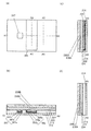
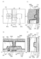
- 3A to 3D are a top view and cross-sectional views of a semiconductor device according to one embodiment of the present invention.
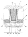
- FIG. 4 is a cross-sectional view of a semiconductor device according to one embodiment of the present invention.
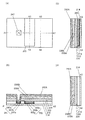
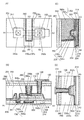
- 7A to 7D are a top view and cross-sectional views illustrating a method for manufacturing a semiconductor device according to one embodiment of the present invention.
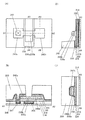
- 7A to 7D are a top view and cross-sectional views illustrating a method for manufacturing a semiconductor device according to one embodiment of the present invention.
- 7A to 7D are a top view and cross-sectional views illustrating a method for manufacturing a semiconductor device according to one embodiment of the present invention.
- 7A to 7D are a top view and cross-sectional views illustrating a method for manufacturing a semiconductor device according to one embodiment of the present invention.
- 7A to 7D are a top view and cross-sectional views illustrating a method for manufacturing a semiconductor device according to one embodiment of the present invention.
- 7A to 7D are a top view and cross-sectional views illustrating a method for manufacturing a semiconductor device according to one embodiment of the present invention.
- 7A to 7D are a top view and cross-sectional views illustrating a method for manufacturing a semiconductor device according to one embodiment of the present invention.
- 7A to 7D are a top view and cross-sectional views illustrating a method for manufacturing a semiconductor device according to one embodiment of the present invention.
- 7A to 7D are a top view and cross-sectional views illustrating a method for manufacturing a semiconductor device according to one embodiment of the present invention.
- 7A to 7D are a top view and cross-sectional views illustrating a method for manufacturing a semiconductor device according to one embodiment of the present invention.
- 7A to 7D are a top view and cross-sectional views illustrating a method for manufacturing a semiconductor device according to one embodiment of the present invention.
- 7A to 7D are a top view and cross-sectional views illustrating a method for manufacturing a semiconductor device according to one embodiment of the present invention.
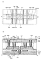
- 3A to 3D are a top view and cross-sectional views of a semiconductor device according to one embodiment of the present invention.
- FIG. 13 is a cross-sectional view illustrating a structure of a memory device according to one embodiment of the present invention.
- FIG. 13 is a cross-sectional view illustrating a structure of a memory device according to one embodiment of the present invention.
- FIG. 13 is a cross-sectional view illustrating a structure of a memory device according to one embodiment of the present invention.
- FIG. 13 is a cross-sectional view illustrating a structure of a memory device according to one embodiment of the present invention.
- FIG. 13 is a cross-sectional view illustrating a structure of a memory device according to one embodiment of the present invention.
- FIGS. 1 is a cross-sectional view illustrating a structure of a memory device according to one embodiment of the present invention.
- FIGS. 4A and 4B are block diagrams illustrating a configuration example of a storage device according to one embodiment of the present invention.
- FIGS. FIGS. 3A to 3H are circuit diagrams illustrating a configuration example of a memory device according to one embodiment of the present invention.
- FIGS. 3A and 3B are schematic diagrams of a semiconductor device according to one embodiment of the present invention.
- FIGS. 4A to 4E are schematic diagrams of a memory device according to one embodiment of the present invention.
- FIGS. 6A to 6H illustrate an electronic device according to one embodiment of the present invention.
- ⁇ ⁇ Particular elements may be omitted in some cases, particularly in a top view (also referred to as a “plan view”) or a perspective view, in order to facilitate understanding of the present invention.
- a top view also referred to as a “plan view”
- a perspective view in order to facilitate understanding of the present invention.
- some hidden lines and the like may be omitted.
- ordinal numbers given as first, second, etc. are used for convenience, and do not indicate the order of steps or the order of lamination. Therefore, for example, the description can be made by appropriately replacing “first” with “second” or “third”.
- ordinal numbers described in this specification and the like do not always coincide with ordinal numbers used for specifying one embodiment of the present invention.
- connection relation is not limited to the predetermined connection relation, for example, the connection relation shown in the figure or the text, and it is assumed that anything other than the connection relation shown in the figure or the text is disclosed in the figure or the text.
- X and Y are objects (for example, devices, elements, circuits, wirings, electrodes, terminals, conductive films, layers, and the like).
- the functions of the source and the drain may be switched when transistors having different polarities are used or when the direction of current changes in circuit operation. Therefore, in this specification and the like, the terms of source and drain may be used interchangeably.
- a channel width in a region where a channel is actually formed corresponds to a channel width (hereinafter, also referred to as an “effective channel width”.
- the effective channel width when the gate electrode covers the side surface of the semiconductor, the effective channel width becomes larger than the apparent channel width, and the effect may not be ignored.
- the proportion of a channel formation region formed on the side surface of the semiconductor may be large. In that case, the effective channel width is larger than the apparent channel width.
- a simple term “channel width” may refer to an apparent channel width.
- a simple term “channel width” may refer to an effective channel width. The values of the channel length, the channel width, the effective channel width, the apparent channel width, and the like can be determined by analyzing a cross-sectional TEM image or the like.
- an impurity in a semiconductor refers to, for example, elements other than the main components of the semiconductor.
- an element having a concentration of less than 0.1 atomic% can be regarded as an impurity.
- the impurity is contained, for example, the DOS (Density of State) of the semiconductor may be increased, or the crystallinity may be reduced.
- the impurity that changes the characteristics of the semiconductor include a Group 1 element, a Group 2 element, a Group 13 element, a Group 14 element, a Group 15 element, and an oxide semiconductor.
- transition metals other than the main components such as hydrogen, lithium, sodium, silicon, boron, phosphorus, carbon, and nitrogen.
- water may function as an impurity in some cases.
- oxygen vacancies may be formed by entry of impurities, for example.
- the impurity that changes the characteristics of the semiconductor include a Group 1 element, a Group 2 element, a Group 13 element, and a Group 15 element other than oxygen and hydrogen.
- silicon oxynitride has a higher oxygen content than nitrogen as its composition.
- silicon nitride oxide has a higher nitrogen content than oxygen as its composition.
- the term “insulator” can be replaced with an insulating film or an insulating layer.
- the term “conductor” can be referred to as a conductive film or a conductive layer.
- the term “semiconductor” can be referred to as a semiconductor film or a semiconductor layer.
- parallel refers to a state where two straight lines are arranged at an angle of ⁇ 10 degrees or more and 10 degrees or less. Therefore, a case where the angle is ⁇ 5 degrees or more and 5 degrees or less is also included.
- substantially parallel refers to a state in which two straight lines are arranged at an angle of ⁇ 30 degrees or more and 30 degrees or less.
- Vertical refers to a state in which two straight lines are arranged at an angle of 80 degrees or more and 100 degrees or less. Therefore, a case where the angle is 85 degrees or more and 95 degrees or less is also included.
- substantially perpendicular refers to a state in which two straight lines are arranged at an angle of 60 degrees or more and 120 degrees or less.
- a barrier film is a film having a function of suppressing permeation of impurities such as water and hydrogen and oxygen, and in the case where the barrier film has conductivity, a conductive barrier film is used. May be called.
- a metal oxide is a metal oxide in a broad sense. Metal oxides are classified into oxide insulators, oxide conductors (including transparent oxide conductors), oxide semiconductors (also referred to as oxide semiconductors or simply OS), and the like. For example, in the case where a metal oxide is used for a semiconductor layer of a transistor, the metal oxide may be referred to as an oxide semiconductor in some cases. That is, a transistor including an oxide or an oxide semiconductor can be referred to as a transistor including an OS @ FET or an OS transistor.
- normally-off means that when a potential is not applied to a gate or a ground potential is applied to a gate, a current per 1 ⁇ m of a channel width flowing through a transistor is 1 ⁇ 10 ⁇ 20 at room temperature. A or lower, 1 ⁇ 10 ⁇ 18 A or lower at 85 ° C., or 1 ⁇ 10 ⁇ 16 A or lower at 125 ° C.
- ⁇ Configuration example of semiconductor device> 1A, 1B, 1C, and 1D are a top view and a cross-sectional view of a semiconductor device including the transistor 200 and the capacitor 100 according to one embodiment of the present invention. is there.
- FIG. 1A is a top view of a semiconductor device including the transistor 200 and the capacitor 100.
- FIG. FIGS. 1B, 1C, and 1D are cross-sectional views of the semiconductor device.
- FIG. 1B is a cross-sectional view of a portion indicated by a dashed line A1-A2 in FIG. 1A, and is also a cross-sectional view of the transistor 200 in a channel length direction.
- FIG. 1C is a cross-sectional view of a portion indicated by a dashed-dotted line A3-A4 in FIG. 1A, and is also a cross-sectional view of the transistor 200 in the channel width direction.
- FIG. 1B is a cross-sectional view of a portion indicated by a dashed line A1-A2 in FIG. 1A, and is also a cross-sectional view of the transistor 200 in a channel length direction.
- FIG. 1C is a cross-sectional view of a portion indicated by a dashed-dotted line A
- 1D is a cross-sectional view of a portion indicated by a dashed-dotted line A5 to A6 in FIG. 1A, and is also a cross-sectional view of a source region or a drain region of the transistor 200 in a channel width direction. Note that for simplification of the drawing, some components are not illustrated in the top view in FIG.
- the semiconductor device of one embodiment of the present invention includes an insulator 214 over a substrate (not illustrated), a transistor 200 over the insulator 214, an insulator 280 over an insulator 256 provided over the transistor 200, An insulator 282 over the insulator 280 and an insulator 281 over the insulator 282 are provided.
- the insulator 214, the insulator 280, the insulator 282, and the insulator 281 function as an interlayer film. As illustrated in FIG. 1, at least a part of the transistor 200 and the capacitor 100 are embedded in the insulator 280 and arranged.
- the transistor 200 includes a semiconductor layer, a first gate, a second gate, a source, and a drain. Further, a conductor 247 is provided below the semiconductor layer of the transistor 200. One of a source and a drain of the transistor 200 is in contact with the conductor 247 below the semiconductor layer, and the other of the source and the drain of the transistor 200 is in contact with one of the electrodes of the capacitor 100 above the semiconductor layer. Touch
- the capacitor 100 is provided in the opening formed in the insulator 256, the insulator 280, the insulator 282, and the insulator 281 so as to reach the other of the source and the drain of the transistor 200.
- the capacitor 100 includes a conductor 110 that is in contact with the other top surface of the source and the drain of the transistor 200 at the opening; an insulator 130 that is provided over the conductor 110 and the insulator 281; And a conductor 120 to be arranged.
- the conductor 110 is preferably disposed along the side and bottom surfaces of the opening.
- an insulator 241 be provided between the conductor 110 and the insulator 280.
- the insulator 241 preferably has a function of suppressing diffusion of hydrogen (for example, at least one of a hydrogen atom and a hydrogen molecule).
- the insulator 241 preferably has a function of suppressing diffusion of oxygen (for example, at least one of an oxygen atom and an oxygen molecule).
- the insulator 241 preferably has lower permeability to one or both of oxygen and hydrogen than the insulator 280.
- Transistor 200 Hereinafter, a typical structure of the transistor 200 will be described. Note that the structure of the transistor 200 described below is one embodiment of the present invention, and the present invention is not limited to this. The structure of the transistor 200 can be changed as appropriate in accordance with the function required for the semiconductor device.
- the transistor 200 includes an insulator 216 over the insulator 214, a conductor 205 arranged to be embedded in the insulator 216, an insulator 216 over the insulator 216, and an insulator over the conductor 205.
- an insulator 224 on the insulator 222 an oxide 230a on the insulator 224, an oxide 230b on the oxide 230a, a conductor 242a and a conductor 242b on the oxide 230b, and an oxide 230b
- the side of the oxide 230b, the side of the conductor 242a, the upper surface of the conductor 242a, the side of the conductor 242b, and the conductor 2 It has an insulator 256 which is in contact with the upper surface of the 2b, and.
- the oxide 230c is in contact with the side surface of the conductor 242a and the side surface of the conductor 242b.
- the conductor 260 has a conductor 260a and a conductor 260b, and the conductor 260a is arranged so as to cover the bottom and side surfaces of the conductor 260b.
- the height of the top surface of the conductor 260 is approximately equal to the height of the top surface of the insulator 250, the top surface of the oxide 230c, and the top surface of the insulator 280.
- the insulator 282 is in contact with the top surfaces of the conductor 260, the oxide 230c, the insulator 250, and the insulator 280.
- an opening is formed in the insulator 216, and the conductor 247 described above is arranged in the opening. At least a portion of the upper surface of the conductor 247 is exposed from the insulator 216, and the height of the upper surface of the conductor 247 preferably approximately matches the height of the upper surface of the insulator 216.
- the conductor 247 electrically connects a transistor, a circuit element such as a switch, a transistor, a capacitor, an inductor, a resistor, or a diode, a wiring, an electrode, or a terminal provided below the insulator 214 to the transistor 200. It functions as a plug or a wiring for making an electrical connection.
- the conductor 247 may be electrically connected to a gate, a source, or a drain of a transistor provided below the insulator 214.
- openings that expose at least part of the conductor 247 are formed in the insulator 222, the insulator 224, the oxide 230a, and the oxide 230b.
- the conductor 242a is provided over the oxide 230b and is in contact with at least a part of the top surface of the conductor 247 through the opening. Further, the conductor 242a may be in contact with the side surface of the oxide 230a and the side surface of the oxide 230b inside the opening. In this manner, by connecting the conductor 242a and the conductor 247, electric resistance between the source or the drain of the transistor 200 and the conductor 247 can be reduced. With such a structure, the frequency characteristics and the electrical characteristics of the semiconductor device including the transistor 200 can be improved.
- a circuit element, a wiring, an electrode, or a terminal which is electrically connected to the conductor 247, such as a switch, a transistor, a capacitor, an inductor, a resistor, or a diode overlaps with the oxide 230. Is preferred. Accordingly, the area occupied by the transistor 200, the circuit element, the wiring, the electrode, or the terminal in a top view can be reduced, so that the semiconductor device according to this embodiment can be miniaturized or highly integrated. .
- the semiconductor device described in this embodiment can also be used as a memory cell of a memory device.
- the conductor 247 may be electrically connected to the sense amplifier.
- the sense amplifier may not function when the parasitic capacitance of the conductor 247 and a wiring connecting the conductor 247 and the sense amplifier is excessively larger than the capacitance of the capacitor 100.
- the parasitic capacitance is reduced as compared with the case where the conductor 247 is provided above the conductor 242a. .
- the wiring does not need to be routed over the transistor 200; therefore, the wiring connecting the conductor 247 and the sense amplifier can be shortened and the parasitic capacitance of the wiring can be reduced.
- the conductor 247 under the oxide 230 the parasitic capacitance generated between the conductor 247 and the conductor 260 and the parasitic capacitance generated between the conductor 247 and the conductor 120 can be reduced. Can be.
- the capacitor 100 may be provided so that the capacitor 100 is included in a range of the oxide 230b in a top view in some cases.
- the length of the conductor 110 in the channel width direction is smaller than the length of the oxide 230b in the channel width direction. Therefore, the capacitor 100 can be provided without increasing the occupied area in a top view, so that the semiconductor device according to this embodiment can be miniaturized or highly integrated.
- the conductor 247 is provided below the conductor 242a; however, the semiconductor device described in this embodiment is not limited to this.
- a structure in which the conductor 247 is provided below the conductor 242b may be employed, or a structure in which the conductor 247 is provided under both the conductor 242a and the conductor 242b may be employed.
- the insulator 214, the insulator 222, the insulator 256, the insulator 282, and the insulator 281 preferably have a function of suppressing at least one diffusion of hydrogen (eg, a hydrogen atom or a hydrogen molecule). Further, the insulator 214, the insulator 222, the insulator 256, the insulator 282, and the insulator 281 preferably have a function of suppressing diffusion of oxygen (for example, at least one of oxygen atoms and oxygen molecules).
- the insulator 214, the insulator 222, the insulator 256, the insulator 282, and the insulator 281 each include one or both of oxygen and hydrogen more than any of the insulator 224, the insulator 250, and the insulator 280.
- the permeability is low.
- the conductor 242a and the conductor 242b are provided over the oxide 230b, and the insulator 256 includes an upper surface and a side surface of the conductor 242a, an upper surface and a side surface of the conductor 242b, and an oxide. It is preferable to be in contact with the side surface of the object 230b, the side surface of the oxide 230a, and the upper surface of the insulator 224. Note that the insulator 256 may have a single-layer structure or a stacked structure. Thus, the side surfaces of the oxide 230a and the oxide 230b do not contact the conductor 242a and the conductor 242b except for the opening, that is, on the outer peripheral side surface.
- the insulator 280 is separated from the insulator 224, the oxide 230a, and the oxide 230b by the insulator 256.
- the conductor 260 functions as a gate electrode of the transistor, and the conductor 242a and the conductor 242b each function as a source electrode or a drain electrode.
- a conductor 260 functioning as a gate electrode is formed in a self-aligned manner so as to fill an opening formed in the insulator 280 or the like. By forming the conductor 260 in this manner, the conductor 260 can be reliably arranged in a region between the conductor 242a and the conductor 242b without alignment.
- the oxide 230 includes an oxide 230a over the insulator 224, an oxide 230b over the oxide 230a, and an oxide 230c which is provided over the oxide 230b and at least part of which is in contact with the top surface of the oxide 230b. Is preferable.
- the oxide 230 in a region where a channel is formed (hereinafter, also referred to as a channel formation region) and in the vicinity thereof, the oxide 230 has a three-layer structure of an oxide 230a, an oxide 230b, and an oxide 230c.
- the present invention is not limited to this.
- the oxide 230 has a single-layer structure of the oxide 230b, a two-layer structure of the oxide 230b and the oxide 230a, a two-layer structure of the oxide 230b and the oxide 230c, or a stacked structure of four or more layers. Is also good.
- each of the oxide 230a, the oxide 230b, and the oxide 230c may have a stacked structure of two or more layers.
- a metal oxide functioning as an oxide semiconductor (hereinafter, also referred to as an oxide semiconductor) is used for the oxide 230 including the channel formation region (the oxide 230a, the oxide 230b, and the oxide 230c). Is preferred.
- the transistor 200 including an oxide semiconductor in a channel formation region has extremely low leakage current (off current) in a non-conduction state; thus, a semiconductor device with low power consumption can be provided. Further, since an oxide semiconductor can be formed by a sputtering method or the like, it can be used for the transistor 200 included in a highly integrated semiconductor device.
- an In-M-Zn oxide (element M is aluminum, gallium, yttrium, tin, copper, vanadium, beryllium, boron, titanium, iron, nickel, germanium, zirconium, molybdenum, lanthanum, cerium , Neodymium, hafnium, tantalum, tungsten, or magnesium, or a plurality thereof).
- element M aluminum, gallium, yttrium, or tin is preferably used.
- an In-Ga oxide or an In-Zn oxide may be used as the oxide 230.
- the carrier density is increased and the resistance may be reduced in some cases. Further, when the concentration of oxygen contained in the oxide 230 decreases, the carrier density increases and the resistance may be reduced in some cases.
- the conductor 242 (the conductor 242a and the conductor 242b) which is provided so as to be in contact with the oxide 230b and functions as a source electrode or a drain electrode has a function of absorbing oxygen of the oxide 230, or
- the oxide 230 has a function of supplying impurities such as hydrogen, nitrogen, or a metal element
- a low-resistance region may be partially formed in the oxide 230 in some cases.
- the conductor 242 is formed over the oxide 230b, and does not contact the side surfaces of the oxide 230a and the oxide 230b and the insulator 224 other than the opening reaching the conductor 247, that is, the outer peripheral side surface.
- oxygen contained in the oxide 230a and the oxide 230b particularly, oxygen contained in the channel formation region and the vicinity thereof can be suppressed from being absorbed by the conductor 242 from the side surfaces of the oxide 230a and the oxide 230b. .
- the insulator 256 is provided so that the side surfaces of the oxide 230a and the oxide 230b do not directly contact the insulator 280. Further, it is provided to suppress oxidation of the conductor 242. Note that in the case where the conductivity does not significantly decrease even when the conductor 242 absorbs an oxidation-resistant material or oxygen, the insulator 256 does not need to have an effect of suppressing oxidation of the conductor 242.
- FIG. 2 is an enlarged view of the vicinity of the channel formation region in FIG.
- a conductor 242 is provided so as to be in contact with the oxide 230b, and a region 249 (a region 249a, a region 249a, And a region 249b) are formed.
- the oxide 230 includes a region 234 functioning as a channel formation region of the transistor 200, a region 231 (a region 231a and a region 231b) functioning as a source or drain region, and a region 232 (a region 232) between the region 234 and the region 231. 232a and a region 232b).
- the area 231 includes the area 249.
- FIG. 2 illustrates an example in which the oxide 230c has a single-layer structure; however, this embodiment is not limited thereto.
- the oxide 230c may have a stacked structure of two or more layers.
- the region 231 functioning as a source or drain region has a low oxygen concentration or an impurity including hydrogen, nitrogen, a metal element, or the like; It is. That is, the region 231 has a higher carrier density and a lower resistance than the region 234.
- the region 234 functioning as a channel formation region is a high-resistance region having a low carrier density because the oxygen concentration is higher or the impurity concentration is lower than that of the region 249 in the region 231, in particular.
- the oxygen concentration of the region 232 is preferably equal to or higher than the oxygen concentration of the region 231, and is preferably equal to or lower than the oxygen concentration of the region 234.
- the impurity concentration of the region 232 is preferably equal to or lower than the impurity concentration of the region 231, and is preferably equal to or higher than the impurity concentration of the region 234.
- the region 232 has approximately the same resistance as the region 234 depending on the concentration of oxygen and the concentration of impurities contained therein, so that the region 232 functions as a channel formation region in the same manner as the region 234.
- the low-resistance region functions as a low-resistance region having approximately the same resistance value or has a higher resistance than the region 231 and a lower resistance than the region 234.
- impurities included in the region 231 are easily diffused in the ab plane direction, and the resistance of the region 232 may be reduced.
- the region 249 which is a low-resistance region includes a metal element
- the region 249 includes, in addition to the metal element included in the oxide 230, aluminum, chromium, copper, silver, gold, platinum, tantalum, nickel, titanium, Molybdenum, tungsten, hafnium, vanadium, niobium, manganese, magnesium, zirconium, beryllium, indium, ruthenium, iridium, strontium, preferably having one or more metal elements selected from metal elements such as lanthanum .
- the region 249 is formed near the interface between the oxide 230b and the conductor 242 in the thickness direction of the oxide 230b; however, this embodiment is not limited to this.
- the region 249 may have substantially the same thickness as the oxide 230b, or may be formed in the oxide 230a.
- the region 249 is formed only in the region 231 in FIG. 2, this embodiment is not limited to this.
- the region 249 may be formed in the region 231 and the region 232, or may be formed in the region 231 and part of the region 232. Alternatively, it may be formed in the region 231, the region 232, and a part of the region 234.
- concentrations of metal elements and impurity elements such as hydrogen and nitrogen detected in each region are not limited to a stepwise change in each region, but also change continuously (also referred to as gradation) in each region. Is also good. That is, the concentration of the metal element and the concentrations of the impurity elements such as hydrogen and nitrogen need only decrease as the region is closer to the channel formation region.
- the conductor 242 for example, aluminum, chromium, copper, silver, gold, platinum, tantalum, nickel, titanium, molybdenum, tungsten, hafnium, vanadium, niobium, It is preferable to use a material containing at least one of a metal element for increasing conductivity, such as manganese, magnesium, zirconium, beryllium, indium, ruthenium, iridium, strontium, and lanthanum, and an impurity.
- a metal element for increasing conductivity such as manganese, magnesium, zirconium, beryllium, indium, ruthenium, iridium, strontium, and lanthanum, and an impurity.
- the conductive film 242A to be the conductor 242 a material or a film formation method in which an impurity such as an element forming an oxygen vacancy or an element captured by the oxygen vacancy is injected into the oxide 230 is used.
- the element includes hydrogen, boron, carbon, nitrogen, fluorine, phosphorus, sulfur, chlorine, a rare gas element, and the like.
- the rare gas element include helium, neon, argon, krypton, and xenon.
- a transistor including an oxide semiconductor when impurities and oxygen vacancies are present in a region where a channel is formed in the oxide semiconductor, electric characteristics are likely to be changed and reliability may be deteriorated.
- oxygen vacancies when oxygen vacancies are included in a region where a channel is formed in the oxide semiconductor, the transistor is likely to have normally-on characteristics. Therefore, it is preferable that oxygen vacancies in the region 234 where a channel is formed be reduced as much as possible.
- the insulator 250 adjacent to the oxide 230 preferably contains more oxygen (also referred to as excess oxygen) than oxygen that satisfies the stoichiometric composition. Oxygen included in the insulator 250 is diffused into the oxide 230, oxygen vacancies in the oxide 230 are reduced, and normally on transistor can be suppressed.
- oxygen vacancies in the region 234 of the oxide 230 can be reduced by diffusion of oxygen included in the insulator 250 to the region 234 of the oxide 230.
- oxygen in the insulator 280 diffuses into the region 234 of the oxide 230 through the oxide 230c; thus, oxygen vacancies in the region 234 of the oxide 230 can be reduced.
- a material in which oxygen is easily transmitted may be used for a layer of the oxide 230c which is in contact with the insulator 280 with a stacked structure. Accordingly, oxygen contained in the insulator 280 is easily diffused into the region 234 of the oxide 230 through the layer of the oxide 230c.
- Oxygen of the insulator 280 can be efficiently supplied to the region 234 of the oxide 230.
- the supply amount of oxygen to the oxide 230 can be controlled, so that a highly reliable transistor in which normally on is suppressed can be obtained.
- the transistor 200 which is one embodiment of the present invention has a structure in which the insulator 282 and the insulator 250 are in direct contact with each other as illustrated in FIGS.
- oxygen contained in the insulator 280 is less likely to be absorbed by the conductor 260. Therefore, oxygen contained in the insulator 280 can be efficiently supplied to the oxide 230a and the oxide 230b through the oxide 230c; thus, oxygen vacancies in the oxide 230a and the oxide 230b can be reduced.
- electrical characteristics and reliability of the transistor 200 can be improved.
- the entry of impurities such as hydrogen contained in the insulator 280 into the insulator 250 can be suppressed; thus, adverse effects on electrical characteristics and reliability of the transistor 200 can be suppressed.
- the insulator 282 silicon nitride, silicon nitride oxide, aluminum oxide, or hafnium oxide can be used. It is particularly preferable to use silicon nitride as the insulator 282.
- the silicon nitride can suitably block impurities (e.g., hydrogen and water) which can enter from the outside.
- the insulator 256 preferably has a function of suppressing transmission of impurities such as hydrogen and water and oxygen.
- the insulator 256 may have a single-layer structure or a stacked structure of two or more layers.
- As the insulator 256 for example, aluminum oxide, hafnium oxide, a silicon oxide film, a silicon nitride film, or a silicon nitride oxide film can be used.
- the same material may be used for the upper layer and the lower layer, or different materials may be used.
- the upper layer and the lower layer of the insulator 256 may be formed using different deposition methods.
- the lower layer of the insulator 256 may be formed by a sputtering method, and the upper layer of the insulator 256 may be formed by an ALD (Atomic Layer Deposition) method.
- the lower layer of the insulator 256 may be formed by an ALD method, and the upper layer of the insulator 256 may be formed by a sputtering method.
- a material that can be used for the oxide 230 may be used for the insulator 256.
- 1D is a cross-sectional view of a portion indicated by a dashed-dotted line A5-A6 in FIG. 1A, and is also a cross-sectional view of the source or drain region of the transistor 200 in the channel width direction.
- the top surface of the conductor 242b and the side surface of the conductor 242b are covered with an insulator 256, so that the top surface of the conductor 242b and the top surface of the conductor 242b are viewed from the top. It is possible to suppress diffusion of impurities such as hydrogen and water and oxygen into the conductor 242b.
- the height of the bottom surface of the conductor 260 in a region where the oxide 230a and the oxide 230b and the conductor 260 do not overlap with each other with reference to the bottom surface of the insulator 224 is It is preferable to be arranged at a position lower than the height of the bottom surface of the oxide 230b.
- the difference between the height of the bottom surface of the conductor 260 and the height of the bottom surface of the oxide 230b in a region where the oxide 230b and the conductor 260 do not overlap with each other is 0 nm to 100 nm, preferably 3 nm to 50 nm. Or less, more preferably 5 nm or more and 20 nm or less.
- the conductor 260 functioning as a gate electrode covers the side surface and the upper surface of the oxide 230b in the channel formation region with the oxide 230c and the insulator 250 interposed therebetween. It is easy to act on the entire oxide 230b in the formation region. Therefore, the on-state current of the transistor 200 can be increased and frequency characteristics can be improved.
- a miniaturized or highly integrated semiconductor device can be provided.
- a semiconductor device having a transistor with high on-state current can be provided.
- a semiconductor device including a transistor having high frequency characteristics can be provided.
- a semiconductor device including a transistor with low off-state current can be provided.
- the following describes a detailed structure of a semiconductor device including the transistor 200 according to one embodiment of the present invention.
- the conductor 205 is provided so as to overlap with the oxide 230 and the conductor 260. It is preferable that the conductor 205 be provided so as to be embedded in the insulator 216.
- the conductor 260 may function as a first gate (also referred to as a top gate) electrode in some cases.
- the conductor 205 functions as a second gate (also referred to as a bottom gate) electrode.
- the Vth of the transistor 200 can be controlled by changing the potential applied to the conductor 205 independently of the potential applied to the conductor 260 without changing the potential.
- Vth of the transistor 200 can be made higher than 0 V and off-state current can be reduced. Therefore, when a negative potential is applied to the conductor 205, the drain current when the potential applied to the conductor 260 is 0 V can be smaller than when no negative potential is applied.
- the conductor 205 is preferably provided to be larger than a region of the oxide 230 which does not overlap with the conductors 242a and 242b as illustrated in FIG.
- the conductor 205 preferably extends in a region outside an end portion of the oxide 230 that intersects with the channel width direction. That is, it is preferable that the conductor 205 and the conductor 260 overlap with each other with the insulator interposed outside the side surface of the oxide 230 in the channel width direction.
- charge-up local charging
- the conductor 205 may overlap with at least the oxide 230 located between the conductor 242a and the conductor 242b.
- the channel formation region is electrically surrounded by an electric field of the conductor 260 having a function as the first gate electrode and an electric field of the conductor 205 having a function of the second gate electrode.
- a structure of a transistor that electrically surrounds a channel formation region by an electric field of the first gate electrode and the second gate electrode is referred to as a surrounded-channel (S-channel) structure.
- the first conductive layer of the conductor 205 is preferably a conductor which suppresses transmission of impurities such as water or hydrogen and oxygen.
- a conductor which suppresses transmission of impurities such as water or hydrogen and oxygen.
- titanium, titanium nitride, tantalum, or tantalum nitride can be used in a single layer or a stacked layer.
- a conductor having good adhesion to the first and third conductive layers may be used.
- the third conductive layer of the conductor 205 is preferably formed using a conductive material mainly containing tungsten, copper, or aluminum.
- the conductor 205 is illustrated as having three layers, the conductor 205 may have a single-layer structure, a two-layer structure, or a multi-layer structure of four or more layers.
- the insulator 214, the insulator 256, the insulator 282, and the insulator 281 function as a barrier insulating film for preventing impurities such as water or hydrogen from entering the transistor 200 from the substrate side or from above. Is preferred. Therefore, the insulator 214, the insulator 256, the insulator 282, and the insulator 281 are formed using a hydrogen atom, a hydrogen molecule, a water molecule, a nitrogen atom, a nitrogen molecule, a nitrogen oxide molecule (eg, N 2 O, NO, NO 2 ), It is preferable to use an insulating material having a function of suppressing diffusion of an impurity such as a copper atom (the impurity is difficult to transmit). Alternatively, it is preferable to use an insulating material having a function of suppressing diffusion of oxygen (for example, at least one of an oxygen atom and an oxygen molecule) (the above-described oxygen is not easily transmitted).
- a hydrogen atom for example, at least one
- aluminum oxide, hafnium oxide, silicon nitride, or the like for the insulator 214, the insulator 256, the insulator 282, and the insulator 281.
- aluminum oxide may be used for the insulator 214, the insulator 256, and the insulator 282, and aluminum nitride may be used for the insulator 281. Accordingly, diffusion of impurities such as water or hydrogen into the insulator 224, the oxide 230, the insulator 250, and the like can be suppressed.
- the resistivity of the insulator 214, the insulator 256, the insulator 282, and the insulator 281 is approximately 1 ⁇ 10 13 ⁇ cm, so that the insulator 214, the insulator
- the body 256, the insulator 282, and the insulator 281 can reduce charge-up of the conductor 205, the conductor 242, or the conductor 260.
- the insulator 214 may have a laminated structure.
- an aluminum oxide film be used as an upper layer of the insulator 214 and a silicon nitride film be used as a lower layer of the insulator 214.
- Oxygen can be supplied below the insulator 214 with the aluminum oxide film.
- the silicon nitride film diffusion of impurities such as hydrogen and water from the substrate side to the transistor 200 side can be suppressed.
- the insulators 216 and 280 preferably have a lower dielectric constant than the insulator 214.
- a material having a low dielectric constant as an interlayer film, parasitic capacitance generated between wirings can be reduced.
- silicon oxide, silicon oxynitride, silicon nitride oxide, silicon nitride, silicon oxide added with fluorine, silicon oxide added with carbon, silicon oxide added with carbon and nitrogen, or Silicon oxide having holes may be used as appropriate.
- the insulator 222 and the insulator 224 have a function as a gate insulator.
- the insulator 224 in contact with the oxide 230 release oxygen by heating.
- oxygen released by heating may be referred to as excess oxygen.
- the insulator 224 may be formed using silicon oxide or silicon oxynitride as appropriate.
- an oxide material from which part of oxygen is released by heating as the insulator 224.
- An oxide from which oxygen is released by heating means that the amount of oxygen released as oxygen molecules by TDS (Thermal Desorption Spectroscopy) analysis is 1.0 ⁇ 10 18 molecules / cm 3 or more, preferably 1 ⁇ 10 18 molecules / cm 3 or more. .0 ⁇ 10 19 molecules / cm 3 or more, more preferably 2.0 ⁇ 10 19 molecules / cm 3 or more, or 3.0 ⁇ 10 oxide is 20 molecules / cm 3 or more.
- the surface temperature of the film at the time of the TDS analysis is preferably in the range of 100 ° C to 700 ° C, or 100 ° C to 400 ° C.
- the insulator 222 preferably functions as a barrier insulating film for preventing impurities such as water or hydrogen from entering the transistor 200 from the substrate side.
- the insulator 222 preferably has lower hydrogen permeability than the insulator 224.
- the insulator 222 have a function of suppressing diffusion of oxygen (for example, at least one of oxygen atoms and oxygen molecules) (the oxygen is hardly transmitted).
- the insulator 222 preferably has lower oxygen permeability than the insulator 224. It is preferable that the insulator 222 have a function of suppressing diffusion of oxygen and impurities because diffusion of oxygen included in the oxide 230 to a lower side than the insulator 222 can be reduced.
- the conductor 205 can be prevented from reacting with oxygen included in the insulator 224 and the oxide 230.
- an insulator containing an oxide of one or both of aluminum and hafnium which is an insulating material, may be used. It is preferable to use aluminum oxide, hafnium oxide, an oxide containing aluminum and hafnium (hafnium aluminate), or the like as the insulator containing one or both oxides of aluminum and hafnium. In the case where the insulator 222 is formed using such a material, the insulator 222 suppresses release of oxygen from the oxide 230 and entry of impurities such as hydrogen from the periphery of the transistor 200 into the oxide 230. Functions as a layer.
- aluminum oxide, bismuth oxide, germanium oxide, niobium oxide, silicon oxide, titanium oxide, tungsten oxide, yttrium oxide, or zirconium oxide may be added to these insulators.
- these insulators may be nitrided. Silicon oxide, silicon oxynitride, or silicon nitride may be stacked over the above insulator.
- the insulator 222 is formed of, for example, aluminum oxide, hafnium oxide, tantalum oxide, zirconium oxide, lead zirconate titanate (PZT), strontium titanate (SrTiO 3 ), or (Ba, Sr) TiO 3 (BST).
- An insulator including a so-called high-k material may be used in a single layer or a stacked structure. When a transistor is miniaturized and highly integrated, a problem such as a leak current may be caused by thinning of a gate insulator. When a high-k material is used for the insulator functioning as a gate insulator, the gate potential during the operation of the transistor can be reduced while the physical thickness is maintained.
- the insulator 222 and the insulator 224 may have a stacked structure of two or more layers.
- the structure is not limited to the laminated structure made of the same material, and may be a laminated structure made of different materials.
- the conductor 247 includes a first conductive layer, a second conductive layer provided inside the first conductive layer, and a third conductive layer provided inside the second conductive layer. And a conductive layer.
- a conductor which suppresses transmission of impurities such as water or hydrogen and oxygen is preferable.
- titanium, titanium nitride, tantalum, or tantalum nitride can be used.
- a conductor having good adhesion to the first conductive layer and the third conductive layer may be used.
- a conductive material mainly containing tungsten, copper, or aluminum is preferably used.
- the conductor 247 is illustrated as having three layers, the conductor 247 may have a single-layer structure, a two-layer structure, or a multi-layer structure of four or more layers.
- an insulator which suppresses diffusion of impurities such as hydrogen and water and oxygen may be provided on a side surface of the conductor 247.
- the oxide 230 includes an oxide 230a, an oxide 230b over the oxide 230a, and an oxide 230c over the oxide 230b.
- the oxide 230c is provided so as to at least partially overlap with a region between the conductors 242a and 242b.
- the oxide 230a is provided below the oxide 230b, diffusion of impurities from the structure formed below the oxide 230a to the oxide 230b can be suppressed.
- the oxide 230c is provided over the oxide 230b, diffusion of impurities into the oxide 230b from a structure formed above the oxide 230c can be suppressed.
- the oxide 230 preferably has a stacked structure of oxides having different atomic ratios of metal atoms. Specifically, in the metal oxide used for the oxide 230a, the atomic ratio of the element M in the constituent elements is larger than that in the metal oxide used for the oxide 230b. Is preferred. In the metal oxide used for the oxide 230a, the atomic ratio of the element M to In is preferably larger than that in the metal oxide used for the oxide 230b. In the metal oxide used for the oxide 230b, the atomic ratio of In to the element M is preferably larger than that in the metal oxide used for the oxide 230a. Further, as the oxide 230c, a metal oxide which can be used for the oxide 230a or the oxide 230b can be used.
- the oxide 230b preferably has crystallinity.
- a CAAC-OS c-axis / aligned / crystalline / oxide / semiconductor
- An oxide having crystallinity, such as a CAAC-OS has a high density and a dense structure with few impurities and defects (such as oxygen vacancies).
- impurities and defects such as oxygen vacancies.
- the energy of the bottom of the conduction band of the oxide 230a and the oxide 230c be higher than the energy of the bottom of the conduction band of the oxide 230b.
- the electron affinity of the oxide 230a and the oxide 230c is preferably smaller than the electron affinity of the oxide 230b.
- the energy level at the bottom of the conduction band changes gently.
- the energy level at the bottom of the conduction band at the junction of the oxide 230a, the oxide 230b, and the oxide 230c changes continuously or forms a continuous junction.
- the defect state density of a mixed layer formed at the interface between the oxide 230a and the oxide 230b and the interface between the oxide 230b and the oxide 230c may be reduced.
- the oxide 230c has a stacked structure
- In: Ga: Zn 4: 2: 3 [atomic ratio] as a lower layer of the oxide 230c
- Ga: A stacked structure of Zn 2: 1 [atomic ratio]
- In: Ga: Zn 4: 2: 3 [atomic ratio] as a lower layer of the oxide 230c
- Ga: Zn 2 as an upper layer of the oxide 230c.
- the main path of the carriers is the oxide 230b.
- the density of defect states at the interface between the oxides 230a and 230b and the interface between the oxides 230b and 230c can be reduced. Therefore, influence of carrier scattering due to interface scattering is small, and the transistor 200 can have high on-state current and high frequency characteristics.
- the oxide 230c has a stacked structure, in addition to the effect of reducing the density of defect states at the interface between the oxide 230b and the oxide 230c, constituent elements of the oxide 230c It is expected to suppress diffusion to More specifically, the oxide 230c has a stacked structure, and an oxide that does not contain In or has a reduced concentration of In is located in the upper layer of the stacked structure, so that In that can diffuse to the insulator 250 side is suppressed. can do. Since the insulator 250 functions as a gate insulator, when In is diffused, the characteristics of the transistor become poor. Therefore, by forming the oxide 230c to have a stacked structure, a highly reliable semiconductor device can be provided.
- a main carrier path may be in the vicinity of the interface between the oxide 230b, the lower layer of the oxide 230c, and the interface.
- oxygen contained in the insulator 280 can be supplied to the channel formation region of the transistor 200 through the lower layer of the oxide 230c. It is preferable that a material through which oxygen is not easily transmitted be used as the upper layer of the oxide 230c. With the use of any of the above materials, oxygen contained in the insulator 280 can be suppressed from penetrating the upper layer of the oxide 230c and being absorbed by the insulator 250 or the conductor 260, so that the channel formation region can be efficiently formed. Oxygen can be supplied.
- the oxide 230 has the region 231 and the region 234. Note that at least a part of the region 231 has a region in contact with the conductor 242.
- one of the region 231a and the region 231b functions as a source region and the other functions as a drain region.
- at least part of the region 234 functions as a region where a channel is formed.
- a metal oxide functioning as an oxide semiconductor is preferably used.
- the off-state current of the transistor can be reduced. With the use of such a transistor, a semiconductor device with low power consumption can be provided.
- the electron affinity or the energy level Ec at the bottom of the conduction band can be obtained from the ionization potential Ip, which is the difference between the vacuum level and the energy Ev at the top of the valence band, and the energy gap Eg.
- the ionization potential Ip can be measured, for example, by using an ultraviolet photoelectron spectroscopy (UPS) device (Ultraviolet @ Photoelectron @ Spectroscopy).
- UPS ultraviolet photoelectron spectroscopy
- the energy gap Eg can be measured using, for example, a spectroscopic ellipsometer.
- a conductor 242 (a conductor 242a and a conductor 242b) functioning as a source electrode and a drain electrode is provided over the oxide 230b.
- the thickness of the conductor 242 may be, for example, 1 nm to 50 nm, preferably 2 nm to 25 nm.
- the conductor 242 aluminum, chromium, copper, silver, gold, platinum, tantalum, nickel, titanium, molybdenum, tungsten, hafnium, vanadium, niobium, manganese, magnesium, zirconium, beryllium, indium, ruthenium, iridium, strontium, It is preferable to use a metal element selected from lanthanum, an alloy containing the above-described metal element as a component, an alloy in which the above-described metal elements are combined, or the like.
- tantalum nitride, titanium nitride, tungsten, a nitride containing titanium and aluminum, a nitride containing tantalum and aluminum, ruthenium oxide, ruthenium nitride, an oxide containing strontium and ruthenium, an oxide containing lanthanum and nickel, and the like are used. Is preferred.
- tantalum nitride, titanium nitride, nitride containing titanium and aluminum, nitride containing tantalum and aluminum, ruthenium oxide, ruthenium nitride, oxide containing strontium and ruthenium, and oxide containing lanthanum and nickel are not easily oxidized.
- a conductive material or a material which maintains conductivity even when oxygen is absorbed is preferable.
- the insulator 250 functions as a gate insulator.
- the insulator 250 is preferably provided in contact with the upper surface of the oxide 230c.
- silicon oxide, silicon oxynitride, silicon nitride oxide, silicon nitride, silicon oxide to which fluorine is added, silicon oxide to which carbon is added, silicon oxide to which carbon and nitrogen are added, or silicon oxide having holes is used. be able to.
- silicon oxide and silicon oxynitride are preferable because they are stable against heat.
- the insulator 250 may be formed using an insulator from which oxygen is released by heating.
- an insulator from which oxygen is released by heating is provided as the insulator 250 in contact with the upper surface of the oxide 230c, oxygen can be effectively supplied to a channel formation region of the oxide 230b.
- the concentration of impurities such as water or hydrogen in the insulator 250 is preferably reduced.
- the thickness of the insulator 250 is preferably greater than or equal to 1 nm and less than or equal to 20 nm.
- a metal oxide may be provided between the insulator 250 and the conductor 260. It is preferable that the metal oxide suppress oxygen diffusion from the insulator 250 to the conductor 260. By providing a metal oxide that suppresses diffusion of oxygen, diffusion of oxygen from the insulator 250 to the conductor 260 is suppressed. That is, a decrease in the amount of oxygen supplied to the oxide 230 can be suppressed. Further, oxidation of the conductor 260 due to oxygen of the insulator 250 can be suppressed.
- the metal oxide may function as part of a gate insulator in some cases. Therefore, in the case where silicon oxide, silicon oxynitride, or the like is used for the insulator 250, the metal oxide is preferably a high-k metal oxide having a high relative dielectric constant.
- the gate insulator has a stacked structure of the insulator 250 and the metal oxide, a stacked structure which is stable against heat and has a high relative dielectric constant can be obtained. Therefore, it is possible to reduce the gate potential applied during the operation of the transistor while maintaining the physical thickness of the gate insulator. Further, the equivalent oxide thickness (EOT) of the insulator functioning as a gate insulator can be reduced.
- EOT equivalent oxide thickness
- hafnium, aluminum, gallium, yttrium, zirconium, tungsten, titanium, tantalum, nickel, germanium, or magnesium, or a metal oxide containing two or more kinds may be used. it can.
- the metal oxide may have a function as part of the gate electrode.
- a conductive material containing oxygen is preferably provided on the channel formation region side.
- a conductor functioning as a gate electrode a conductive material containing a metal element and oxygen contained in a metal oxide in which a channel is formed is preferably used. Further, a conductive material containing the above-described metal element and nitrogen may be used. In addition, indium tin oxide, indium oxide containing tungsten oxide, indium zinc oxide containing tungsten oxide, indium oxide containing titanium oxide, indium tin oxide containing titanium oxide, indium zinc oxide, and silicon were added. Indium tin oxide may be used. Alternatively, indium gallium zinc oxide containing nitrogen may be used. By using such a material, hydrogen contained in a metal oxide in which a channel is formed may be captured in some cases. Alternatively, in some cases, hydrogen mixed in from an outer insulator or the like can be captured.
- the conductor 260 is illustrated as having a two-layer structure, but the present invention is not limited to this.
- the conductor 260 may have a single-layer structure or a stacked structure of three or more layers.
- Conductor 260a is a hydrogen atom, a hydrogen molecule, a water molecule, a nitrogen atom, a nitrogen molecule, nitric oxide molecule (N 2 O, NO, etc. NO 2), conductive having a function of suppressing the diffusion of impurities such as copper atoms It is preferable to use a material. Alternatively, it is preferable to use a conductive material having a function of suppressing diffusion of oxygen (for example, at least one of oxygen atoms and oxygen molecules).
- the conductor 260a has a function of suppressing diffusion of oxygen, it is possible to prevent the conductor 260b from being oxidized by oxygen contained in the insulator 250 and lowering the conductivity.
- the conductive material having a function of suppressing diffusion of oxygen for example, tantalum, tantalum nitride, ruthenium, ruthenium oxide, or the like is preferably used.
- the conductor 260b be formed using a conductive material mainly containing tungsten, copper, or aluminum.
- a conductor having high conductivity is preferably used.
- a conductive material containing tungsten, copper, or aluminum as a main component can be used.
- the conductor 260b may have a stacked structure, for example, a stacked structure of titanium, titanium nitride, and the above conductive material.
- the insulator 280 includes, for example, silicon oxide, silicon oxynitride, silicon nitride oxide, silicon oxide to which fluorine is added, silicon oxide to which carbon is added, silicon oxide to which carbon and nitrogen are added, or silicon oxide having holes. It is preferred to have. In particular, silicon oxide and silicon oxynitride are preferable because they are thermally stable. In particular, a material such as silicon oxide, silicon oxynitride, or silicon oxide having vacancies is preferable because a region containing oxygen which is released by heating can be easily formed. In order to supply oxygen contained in the insulator 280 to the oxide 230c or the oxide 230b through a lower layer of the oxide 230c, the insulator 280 preferably contains more oxygen. It preferably contains more oxygen than the stoichiometric ratio. In order to increase the concentration of oxygen contained in the insulator 280, the deposition gas used for forming the insulator 280 preferably contains oxygen.
- the concentration of impurities such as water or hydrogen in the insulator 280 be reduced.
- the insulator 280 is preferably formed by a sputtering method, because the insulator 280 in which the concentration of impurities such as water or hydrogen is reduced can be obtained.
- silicon oxynitride are suitable for the insulator 280 because the hydrogen concentration in the film is lower.
- the insulator 280 is formed by a CVD method. It may be formed. Although not illustrated, the insulator 280 may have a stacked structure of two or more layers, and may be formed using silicon oxide formed as a first layer using a sputtering method and formed as a second layer using a CVD method. A stacked body including silicon oxynitride may be used. Further, the upper surface of the insulator 280 may be planarized.
- the insulator 282 and the insulator 281 function as barrier insulating films that prevent impurities such as water or hydrogen from entering the insulator 280 from above.
- an insulator such as aluminum oxide, silicon nitride, or silicon nitride oxide may be used.
- aluminum oxide may be used for the insulator 282 and silicon nitride may be used for the insulator 281.
- oxygen can be supplied to the insulator 280.
- the silicon nitride film used for the insulator 281 diffusion of impurities such as hydrogen and water from above to the transistor 200 side can be suppressed.
- An insulator such as silicon oxide or silicon oxynitride, which functions as an interlayer film, may be provided between the insulator 282 and the insulator 281.
- the capacitance of the capacitor 100 can be adjusted. It is preferable that the insulator have a reduced concentration of impurities such as water or hydrogen in the film, similarly to the insulator 224 and the like.
- Capacitance element 100 The capacitor 100 is provided in the openings formed in the insulator 256, the insulator 280, the insulator 282, and the insulator 281 and is in contact with the upper surface of the conductor 242b. And a conductor 120 on the insulator 130.
- the conductor 110, the insulator 130, and the conductor 120 are arranged in openings formed in the insulator 256, the insulator 280, the insulator 282, and the insulator 281.
- the conductor 110 functions as a lower electrode of the capacitor 100
- the conductor 120 functions as an upper electrode of the capacitor 100
- the insulator 130 functions as a dielectric of the capacitor 100.
- the capacitor 100 has a structure in which the upper electrode and the lower electrode face each other not only on the bottom surface but also on the side surfaces of the opening of the insulator 256, the insulator 280, the insulator 282, and the insulator 281 with the dielectric interposed therebetween.
- the capacitance per unit area can be increased. Therefore, the capacitance of the capacitor 100 can be increased as the depth of the opening is increased.
- miniaturization or high integration of the semiconductor device can be promoted.
- the shape of the opening formed in the insulator 256, the insulator 280, the insulator 282, and the insulator 281 as viewed from above may be a quadrangle, a polygon other than a quadrangle, or a polygon in a polygon.
- the shape may be a curved shape or a circular shape including an ellipse.
- the capacitor 100 is preferably provided so that the capacitor 100 is included in a range of the oxide 230b in a top view.
- the length of the conductor 110 in the channel width direction is smaller than the length of the oxide 230b in the channel width direction.
- the conductor 110 is arranged along the openings formed in the insulator 256, the insulator 280, the insulator 282, and the insulator 281. It is preferable that the height of a part of the upper surface of the conductor 110 be approximately equal to the height of the upper surface of the insulator 281. The upper surface of the conductor 242b is in contact with the lower surface of the conductor 110. It is preferable that the conductor 110 be formed by an ALD method, a CVD method, or the like, and a conductor that can be used for the conductor 205 or the conductor 242 be used.
- the contact resistance between the conductor 110 and the conductor 242b can be reduced.
- tantalum nitride formed by an ALD method can be used as the conductor 110.
- the insulator 130 is arranged so as to cover the conductor 110 and part of the insulator 281.
- the insulator 130 is preferably formed by an ALD method, a CVD method, or the like.
- the insulator 130 is formed using, for example, silicon oxide, silicon oxynitride, silicon nitride oxide, silicon nitride, zirconium oxide, aluminum oxide, aluminum oxynitride, aluminum nitride oxide, aluminum nitride, hafnium oxide, hafnium oxynitride, hafnium nitride oxide, or nitrided nitride.
- Hafnium or the like may be used, and a single layer or a single layer can be provided.
- an insulating film stacked in the order of zirconium oxide, aluminum oxide, and zirconium oxide can be used.
- a material having a high dielectric strength such as silicon oxynitride, or a high dielectric constant (high-k) material (a material having a high relative dielectric constant) for the insulator 130.
- a stacked structure of a material having a high dielectric strength and a high-k material may be used.
- an insulator of a high-k material gallium oxide, hafnium oxide, zirconium oxide, an oxide containing aluminum and hafnium, an oxynitride containing aluminum and hafnium, an oxide containing silicon and hafnium, silicon and hafnium are given. Oxynitride or nitride containing silicon and hafnium.
- materials having high dielectric strength include silicon oxide, silicon oxynitride, silicon nitride oxide, silicon nitride, silicon oxide added with fluorine, silicon oxide added with carbon, silicon oxide added with carbon and nitrogen, and vacancies. Silicon oxide or resin.
- SiO x formed by an ALD method can be used.
- an insulating film which is stacked in the order of SiN x formed by using the ALD method, SiO x formed by using the PEALD method, and SiN x formed by using the ALD method can be used. By using such an insulator having a large dielectric strength, the dielectric strength is improved, and electrostatic breakdown of the capacitor 100 can be suppressed.
- the conductor 120 is provided so as to fill openings formed in the insulator 256, the insulator 280, the insulator 282, and the insulator 281.
- the conductor 120 preferably has a region overlapping with the insulator 281 with the insulator 130 interposed therebetween. With such a structure, the conductor 120 can be reliably insulated from the conductor 110 via the insulator 130. Further, a portion of the conductor 120 above the insulator 281 may be drawn and formed in a wiring shape.
- the conductor 120 is preferably formed by an ALD method, a CVD method, or the like, and a conductor that can be used for the conductor 205 may be used.
- a stacked film of titanium nitride formed by an ALD method and tungsten formed thereover by a CVD method can be used as the conductor 120. Note that when the adhesion of tungsten to the insulator 130 is sufficiently high, a single-layered film of tungsten formed by a CVD method may be used as the conductor 120.
- a conductor functioning as a wiring may be provided in contact with the upper surface of the conductor 120.
- the conductor is preferably formed using a conductive material mainly containing tungsten, copper, or aluminum. Further, the conductor may have a stacked structure, for example, a stacked structure of titanium, titanium nitride, and the above conductive material. Note that the conductor may be formed so as to be embedded in an opening provided in the insulator.
- the insulator 241 is preferably provided in contact with the insulator 256, the insulator 280, the insulator 282, and the side surface of the opening formed in the insulator 281.
- the conductor 110 is provided in contact with the inner side surface of the insulator 241
- the insulator 130 is provided in contact with the inner side surface of the conductor 110
- the conductor 120 is provided in contact with the inner side surface of the insulator 130.
- an insulator such as aluminum oxide, silicon nitride, or silicon nitride oxide may be used, for example. Since the insulator 241 is provided in contact with the insulator 281, the insulator 282, the insulator 280, and the insulator 256, impurities such as water or hydrogen from the insulator 280 or the like are mixed into the oxide 230 through the conductor 110. Can be suppressed. In addition, oxygen contained in the insulator 280 can be prevented from being absorbed by the conductor 110.
- an insulator substrate As a substrate over which the transistor 200 is formed, an insulator substrate, a semiconductor substrate, or a conductor substrate may be used, for example.
- the insulator substrate include a glass substrate, a quartz substrate, a sapphire substrate, a stabilized zirconia substrate (such as a yttria-stabilized zirconia substrate), and a resin substrate.
- the semiconductor substrate include a semiconductor substrate formed using silicon and germanium, and a compound semiconductor substrate formed using silicon carbide, silicon germanium, gallium arsenide, indium phosphide, zinc oxide, and gallium oxide.
- a semiconductor substrate having an insulator region inside the above-described semiconductor substrate for example, an SOI (Silicon On Insulator) substrate.
- the conductor substrate include a graphite substrate, a metal substrate, an alloy substrate, and a conductive resin substrate.
- a substrate including a metal nitride, a substrate including a metal oxide, and the like can be given.
- a substrate provided with a conductor or a semiconductor on an insulator substrate a substrate provided with a conductor or an insulator on a semiconductor substrate, a substrate provided with a semiconductor or an insulator on a conductor substrate, and the like.
- a substrate in which an element is provided may be used.
- Elements provided on the substrate include a capacitor, a resistor, a switch, a light-emitting element, a storage element, and the like.
- the insulator examples include an oxide, a nitride, an oxynitride, a nitride oxide, a metal oxide, a metal oxynitride, and a metal nitride oxide having an insulating property.
- Examples of the insulator having a high relative dielectric constant include gallium oxide, hafnium oxide, zirconium oxide, an oxide containing aluminum and hafnium, an oxynitride containing aluminum and hafnium, an oxide containing silicon and hafnium, and silicon and hafnium. Oxynitride or nitride containing silicon and hafnium.
- the insulator having a low relative dielectric constant includes silicon oxide, silicon oxynitride, silicon nitride oxide, silicon oxide to which fluorine is added, silicon oxide to which carbon is added, silicon oxide to which carbon and nitrogen are added, and holes. Silicon oxide, resin, or the like is given.
- a transistor including an oxide semiconductor can have stable electrical characteristics by being surrounded by an insulator having a function of suppressing transmission of impurities such as hydrogen and oxygen.
- the insulator having a function of suppressing the transmission of impurities such as hydrogen and oxygen include boron, carbon, nitrogen, oxygen, fluorine, magnesium, aluminum, silicon, phosphorus, chlorine, argon, gallium, germanium, yttrium, and zirconium.
- Lanthanum, neodymium, hafnium, or an insulator containing tantalum may be used as a single layer or a stacked layer.
- an insulator having a function of suppressing transmission of impurities such as hydrogen and oxygen
- a metal oxide such as tantalum oxide, or a metal nitride such as aluminum nitride, aluminum titanium nitride, titanium nitride, silicon nitride oxide, or silicon nitride can be used.
- the insulator functioning as a gate insulator is preferably an insulator having a region containing oxygen which is released by heating.
- the oxide 230 oxygen vacancies in the oxide 230 can be compensated.
- Conductors include aluminum, chromium, copper, silver, gold, platinum, tantalum, nickel, titanium, molybdenum, tungsten, hafnium, vanadium, niobium, manganese, magnesium, zirconium, beryllium, indium, ruthenium, iridium, strontium, and lanthanum. It is preferable to use a metal element selected from the above, an alloy containing the above-described metal element as a component, an alloy in which the above-described metal elements are combined, or the like.
- tantalum nitride, titanium nitride, tungsten, a nitride containing titanium and aluminum, a nitride containing tantalum and aluminum, ruthenium oxide, ruthenium nitride, an oxide containing strontium and ruthenium, an oxide containing lanthanum and nickel, and the like are used. Is preferred.
- tantalum nitride, titanium nitride, nitride containing titanium and aluminum, nitride containing tantalum and aluminum, ruthenium oxide, ruthenium nitride, oxide containing strontium and ruthenium, and oxide containing lanthanum and nickel are not easily oxidized.
- a conductive material or a material which maintains conductivity even when oxygen is absorbed is preferable.
- a semiconductor having high electric conductivity represented by polycrystalline silicon containing an impurity element such as phosphorus, or a silicide such as nickel silicide may be used.
- a plurality of conductive layers formed of the above materials may be stacked and used.
- a stacked structure in which the above-described material containing a metal element and a conductive material containing oxygen are combined may be employed.
- a stacked structure in which the above-described material containing a metal element and a conductive material containing nitrogen are combined may be employed.
- a stacked structure of a combination of the above-described material containing a metal element, a conductive material containing oxygen, and a conductive material containing nitrogen may be used.
- a stacked structure in which the above-described material containing a metal element and a conductive material containing oxygen are used for a conductor functioning as a gate electrode is used.
- a conductive material containing oxygen is preferably provided on the channel formation region side.
- a conductor functioning as a gate electrode a conductive material containing a metal element and oxygen contained in a metal oxide in which a channel is formed is preferably used.
- a conductive material containing the above-described metal element and nitrogen may be used.
- a conductive material containing nitrogen such as titanium nitride or tantalum nitride may be used.
- indium tin oxide, indium oxide containing tungsten oxide, indium zinc oxide containing tungsten oxide, indium oxide containing titanium oxide, indium tin oxide containing titanium oxide, indium zinc oxide, and silicon were added.
- Indium tin oxide may be used.
- indium gallium zinc oxide containing nitrogen may be used.
- a metal oxide functioning as an oxide semiconductor is preferably used.
- a metal oxide applicable to the oxide 230 according to the present invention will be described.
- the metal oxide preferably contains at least indium or zinc. In particular, it preferably contains indium and zinc. In addition, it is preferable that aluminum, gallium, yttrium, tin, or the like be contained in addition thereto. Further, one or more kinds selected from boron, titanium, iron, nickel, germanium, zirconium, molybdenum, lanthanum, cerium, neodymium, hafnium, tantalum, tungsten, magnesium, and the like may be contained.
- the metal oxide is an In-M-Zn oxide containing indium, the element M, and zinc is considered.
- the element M is aluminum, gallium, yttrium, tin, or the like.
- Other elements applicable to the element M include boron, titanium, iron, nickel, germanium, zirconium, molybdenum, lanthanum, cerium, neodymium, hafnium, tantalum, tungsten, magnesium, and the like.
- a combination of a plurality of the aforementioned elements may be used as the element M.
- a metal oxide containing nitrogen may be collectively referred to as a metal oxide. Further, a metal oxide containing nitrogen may be referred to as metal oxynitride.
- An oxide semiconductor (metal oxide) is classified into a single crystal oxide semiconductor and a non-single-crystal oxide semiconductor.
- the non-single-crystal oxide semiconductor include a CAAC-OS, a polycrystalline oxide semiconductor, an nc-OS, a pseudo-amorphous oxide semiconductor (a-like OS), and an amorphous oxide semiconductor.
- Semiconductors include a CAAC-OS, a polycrystalline oxide semiconductor, an nc-OS, a pseudo-amorphous oxide semiconductor (a-like OS), and an amorphous oxide semiconductor.
- the CAAC-OS has a c-axis orientation and a crystal structure in which a plurality of nanocrystals are connected in an ab plane direction and has a strain.
- the strain refers to a region where the orientation of the lattice arrangement changes between a region where the lattice arrangement is uniform and a region where another lattice arrangement is uniform in a region where a plurality of nanocrystals are connected.
- a nanocrystal is basically a hexagon, but is not limited to a regular hexagon and may be a non-regular hexagon.
- distortion may have a lattice arrangement such as a pentagon and a heptagon.
- a clear crystal grain boundary also referred to as a grain boundary
- the CAAC-OS can tolerate distortion because the arrangement of oxygen atoms is not dense in the ab plane direction, or the substitution distance of a metal element changes the bonding distance between atoms. That's why.
- the CAAC-OS is a layered crystal in which a layer containing indium and oxygen (hereinafter, an In layer) and a layer containing elements M, zinc, and oxygen (hereinafter, an (M, Zn) layer) are stacked. It tends to have a structure (also called a layered structure).
- indium and the element M can be replaced with each other, and when the element M in the (M, Zn) layer is replaced with indium, it can also be expressed as an (In, M, Zn) layer. Further, when indium in the In layer is replaced with the element M, it can also be referred to as an (In, M) layer.
- CAAC-OS is a metal oxide with high crystallinity.
- the CAAC-OS it is difficult to confirm a clear crystal grain boundary; thus, it can be said that electron mobility due to the crystal grain boundary is hardly reduced.
- CAAC-OS impurities and defects oxygen deficiency (V O: also referred to as oxygen vacancy), etc.) with little metal oxide It can be called a thing. Therefore, a metal oxide having a CAAC-OS has stable physical properties. Therefore, a metal oxide including CAAC-OS is resistant to heat and has high reliability.
- the nc-OS has a periodic atomic arrangement in a minute region (eg, a region with a size from 1 nm to 10 nm, particularly a region with a size from 1 nm to 3 nm).
- a minute region eg, a region with a size from 1 nm to 10 nm, particularly a region with a size from 1 nm to 3 nm.
- the nc-OS may not be distinguished from an a-like @ OS or an amorphous oxide semiconductor depending on an analysis method.
- indium-gallium-zinc oxide which is a kind of metal oxide including indium, gallium, and zinc
- IGZO indium-gallium-zinc oxide
- a smaller crystal for example, the above-described nanocrystal
- a large crystal here, a crystal of several mm or a crystal of several cm.
- it may be structurally stable.
- ⁇ A-like ⁇ OS is a metal oxide having a structure between the nc-OS and an amorphous oxide semiconductor.
- a-like @ OS has voids or low density regions. That is, a-like @ OS has lower crystallinity than the nc-OS and the CAAC-OS.
- Oxide semiconductors have various structures, and each has different characteristics.
- the oxide semiconductor of one embodiment of the present invention may include two or more of an amorphous oxide semiconductor, a polycrystalline oxide semiconductor, an a-like @ OS, an nc-OS, and a CAAC-OS.
- the structure of the oxide semiconductor is not particularly limited, but preferably has crystallinity.
- the oxide 230 can have a CAAC-OS structure. When the oxide 230 has the above crystal structure, a highly reliable semiconductor device can be obtained.
- an oxygen vacancy may be formed in some cases.
- electrons serving as carriers are generated in some cases.
- part of hydrogen may be bonded to oxygen which is bonded to a metal atom to generate an electron serving as a carrier. Therefore, a transistor including a metal oxide containing hydrogen is likely to have normally-on characteristics.
- the hydrogen concentration obtained by SIMS is less than 1 ⁇ 10 20 atoms / cm 3 , preferably less than 1 ⁇ 10 19 atoms / cm 3 , and more preferably 5 ⁇ 10 18 atoms / cm 3. It is less than 3 and more preferably less than 1 ⁇ 10 18 atoms / cm 3 .
- an oxide semiconductor is used as a semiconductor layer of the transistor 200 as one embodiment of the present invention; however, one embodiment of the present invention is not limited thereto.
- silicon, germanium, silicon germanium, silicon carbide, gallium arsenide, aluminum gallium arsenide, indium phosphide, gallium nitride, or Various semiconductor materials such as an organic semiconductor may be included.
- FIGS. 3A to 14A are top views.
- FIG. 2B is a cross-sectional view corresponding to a portion indicated by a dashed-dotted line A1-A2 in FIG. 2A, and is also a cross-sectional view of the transistor 200 in the channel length direction.
- (C) in each drawing is a cross-sectional view corresponding to a portion indicated by a dashed line A3-A4 in (A), and is also a cross-sectional view of the transistor 200 in the channel width direction.
- (D) of each drawing is a cross-sectional view corresponding to a portion indicated by a dashed-dotted line of A5-A6 in (A), and is also a cross-sectional view of the source or drain region of the transistor 200 in the channel width direction. Note that for simplification of the drawings, some components are not illustrated in the top view in FIG.
- a substrate (not shown) is prepared, and an insulator 214 is formed over the substrate.
- the insulator 214 is formed by a sputtering method, a chemical vapor deposition (CVD) method, a molecular beam epitaxy (MBE) method, a pulsed laser deposition (PLD: pulsed laser deposition method), or a molecular beam epitaxy (MBE) method. It can be performed using a method or the like.
- the CVD method can be classified into a plasma CVD (Plasma Enhanced CVD) method using plasma, a thermal CVD (TCVD: Thermal CVD) method using heat, an optical CVD (Photo CVD) method using light, and the like.
- a metal CVD (MCVD: Metal CVD) method and an organic metal CVD (MOCVD: Metal Organic CVD) method can be classified according to a source gas used.
- the thermal CVD method is a film formation method which can reduce plasma damage to an object to be processed because plasma is not used.
- a wiring, an electrode, an element (a transistor, a capacitor, or the like) included in a semiconductor device may be charged up by receiving charge from plasma in some cases. At this time, the accumulated charges may destroy wirings, electrodes, elements, and the like included in the semiconductor device.
- a thermal CVD method that does not use plasma, such plasma damage does not occur, so that the yield of semiconductor devices can be increased.
- plasma damage during film formation does not occur, so that a film with few defects can be obtained.
- the ALD method can deposit atoms one by one using the self-controllability property of atoms, so that an extremely thin film can be formed, a film can be formed on a structure having a high aspect ratio, There are effects that a film having few defects such as holes can be formed, a film having excellent coverage can be formed, and a film can be formed at a low temperature.
- the ALD method also includes a plasma-enhanced PEALD (Plasma Enhanced ALD) method using plasma. The use of plasma enables a film formation at a lower temperature, which is preferable in some cases. Some precursors used in the ALD method contain impurities such as carbon.
- a film formed by an ALD method may contain more impurities such as carbon than a film formed by another film formation method in some cases.
- the impurities can be quantified using X-ray photoelectron spectroscopy (XPS: X-ray @ Photoelectron @ Spectroscopy).
- the CVD method and the ALD method are film formation methods in which a film is formed by a reaction on the surface of an object to be processed, unlike a film formation method in which particles emitted from a target or the like are deposited. Therefore, the film forming method is less affected by the shape of the object to be processed and has good step coverage.
- the ALD method since the ALD method has excellent step coverage and excellent thickness uniformity, it is suitable for covering the surface of an opening having a high aspect ratio.
- the ALD method has a relatively low deposition rate, it may be preferable to use the ALD method in combination with another deposition method such as a CVD method with a high deposition rate.
- the composition of the obtained film can be controlled by the flow ratio of the source gas.
- a film having an arbitrary composition can be formed depending on a flow rate ratio of a source gas.
- a film whose composition is continuously changed can be formed by changing the flow ratio of the source gas while forming the film.
- silicon nitride is formed as the insulator 214 by a CVD method.
- an insulator such as silicon nitride which does not easily transmit copper, as the insulator 214, even when a metal such as copper which is easily diffused is used as a conductor below the insulator 214 (not illustrated), Diffusion of the metal into a layer above the insulator 214 can be suppressed.
- the insulator 216 is formed over the insulator 214.
- the insulator 216 can be formed by a sputtering method, a CVD method, an MBE method, a PLD method, an ALD method, or the like.
- an opening reaching the insulator 214 is formed in the insulator 216.
- the opening includes, for example, a groove and a slit. In some cases, a region where an opening is formed is referred to as an opening.
- the opening may be formed by wet etching, but dry etching is more preferable for fine processing.
- an insulator which functions as an etching stopper film when the insulator 216 is etched to form a groove is preferably selected.
- the insulator 214 may be formed using a silicon nitride film, an aluminum oxide film, or a hafnium oxide film.
- a conductive film to be the conductor 205 and the conductor 247 is formed. It is preferable that the conductive film include a conductor having a function of suppressing transmission of oxygen.
- a conductor having a function of suppressing transmission of oxygen For example, tantalum nitride, tungsten nitride, titanium nitride, or the like can be used. Alternatively, a stacked film of tantalum, tungsten, titanium, molybdenum, aluminum, copper, and a molybdenum tungsten alloy can be used.
- the conductive film to be the conductor 205 and the conductor 247 can be formed by a sputtering method, a CVD method, an MBE method, a PLD method, an ALD method, or the like.
- the conductive film serving as the conductor 205 and the conductor 247 has a multilayer structure.
- tantalum nitride is formed by a sputtering method as a conductive film to be the conductors 205a and 247a
- titanium nitride is formed by a CVD method on the tantalum nitride as a conductive film to be the conductors 205b and 247b.
- Form a film is
- a conductive metal such as copper which is easily diffused can be used as a conductive film to be the conductor 205c and the conductor 247c to be described later. Also, the metal can be prevented from diffusing out of the conductor 205 and the conductor 247.
- a conductive film to be the conductors 205c and 247c is formed.
- the conductive film can be formed by a plating method, a sputtering method, a CVD method, an MBE method, a PLD method, an ALD method, or the like.
- a low-resistance conductive material such as tungsten or copper is formed as the conductive film to be the conductors 205c and 247c.
- tungsten may be formed by a CVD method.
- part of the conductive film to be the conductor 205 and the conductor 247 is removed, so that the insulator 216 is exposed.
- the conductive film to be the conductor 205 and the conductive film to be the conductor 247 remain only in the opening.
- the conductor 205 and the conductor 247 having a flat top surface can be formed (see FIG. 3).
- part of the insulator 216 may be removed by the CMP treatment.
- a conductive film to be the conductor 205 and the conductor 247 is formed over the insulator 214.
- the conductive film can be formed by a sputtering method, a CVD method, an MBE method, a PLD method, an ALD method, or the like. Further, the conductive film can be a multilayer film. In this embodiment, tungsten is formed as the conductive film.
- the conductive film is processed by lithography to form the conductor 205 and the conductor 247.
- a resist mask is formed by removing or leaving the exposed region with a developing solution.
- a conductor, a semiconductor, an insulator, or the like can be processed into a desired shape.
- a resist mask may be formed by exposing the resist using KrF excimer laser light, ArF excimer laser light, EUV (Extreme Ultraviolet) light, or the like.
- a liquid immersion technique may be used in which a liquid (for example, water) is filled between the substrate and the projection lens for exposure.
- an electron beam or an ion beam may be used instead of the above-described light.
- a mask is not required. Note that in removing the resist mask, dry etching such as ashing can be performed, wet etching can be performed, wet etching can be performed after the dry etching, or dry etching can be performed after the wet etching.
- a hard mask made of an insulator or a conductor may be used instead of the resist mask.
- an insulating film or a conductive film serving as a hard mask material is formed over the conductive film serving as the conductors 205 and 247, a resist mask is formed thereover, and the hard mask material is etched.
- a hard mask having a desired shape can be formed.
- the etching of the conductive film to be the conductor 205 and the conductor 247 may be performed after removing the resist mask, or may be performed with the resist mask left. In the latter case, the resist mask may disappear during the etching. After etching the conductive film, the hard mask may be removed by etching.
- the material of the hard mask does not affect the post-process or can be used in the post-process, it is not always necessary to remove the hard mask.
- a capacitively coupled plasma (CCP) etching apparatus having parallel plate electrodes can be used.
- the capacitively coupled plasma etching apparatus having the parallel plate type electrode may be configured to apply a high frequency power to one of the parallel plate type electrodes.
- a configuration in which a plurality of different high-frequency power sources are applied to one of the parallel plate electrodes may be employed.
- a configuration in which a high-frequency power source having the same frequency is applied to each of the parallel plate electrodes may be used.
- a configuration in which a high-frequency power source having a different frequency is applied to each of the parallel plate electrodes may be used.
- a dry etching apparatus having a high-density plasma source can be used.
- a dry etching apparatus having a high-density plasma source for example, an inductively coupled plasma (ICP) etching apparatus or the like can be used.
- ICP inductively coupled plasma
- an insulating film to be the insulator 216 is formed over the insulator 214, the conductor 205, and the conductor 247.
- the insulator to be the insulator 216 can be formed by a sputtering method, a CVD method, an MBE method, a PLD method, an ALD method, or the like.
- silicon oxide is formed by a CVD method.
- the thickness of the insulating film serving as the insulator 216 is preferably greater than or equal to the thickness of the conductor 205 and the conductor 247.
- the thickness of the insulating film to be the insulator 216 is greater than or equal to 1 and less than or equal to 3.
- the thickness of the conductor 205 and the conductor 247 is 150 nm
- the thickness of the insulating film to be the insulator 216 is 350 nm.
- the conductor 205, the conductor 247, and the insulator 216 with a flat top surface can be formed.
- the above is a different method for forming the conductor 205 and the conductor 247.
- the insulator 222 is formed over the insulator 216, the conductor 205, and the conductor 247.
- an insulator containing an oxide of one or both of aluminum and hafnium may be formed. Note that it is preferable to use aluminum oxide, hafnium oxide, an oxide containing aluminum and hafnium (hafnium aluminate), or the like as the insulator containing one or both oxides of aluminum and hafnium.
- An insulator containing an oxide of one or both of aluminum and hafnium has a barrier property to oxygen, hydrogen, and water.
- the insulator 222 has a barrier property to hydrogen and water, diffusion of hydrogen and water included in a structure provided around the transistor 200 to the inside of the transistor 200 through the insulator 222 is suppressed. In addition, generation of oxygen vacancies in the oxide 230 can be suppressed.
- the insulator 222 can be formed by a sputtering method, a CVD method, an MBE method, a PLD method, an ALD method, or the like.
- the insulator 224 is formed over the insulator 222.
- the insulator 224 can be formed by a sputtering method, a CVD method, an MBE method, a PLD method, an ALD method, or the like.
- the heat treatment may be performed at a temperature of 250 ° C to 650 ° C, preferably 300 ° C to 500 ° C, more preferably 320 ° C to 450 ° C.
- the heat treatment is performed in an atmosphere of nitrogen or an inert gas, or an atmosphere containing an oxidizing gas at 10 ppm or more, 1% or more, or 10% or more.
- the heat treatment may be performed in a reduced pressure state.
- heat treatment is performed in an atmosphere including an oxidizing gas at 10 ppm or more, 1% or more, or 10% or more to supplement desorbed oxygen. Good.
- the treatment is continuously performed for one hour at a temperature of 400 ° C. in an oxygen atmosphere.
- impurities such as water and hydrogen contained in the insulator 224 can be removed.
- the heat treatment may be performed after the insulator 222 is formed.
- the above-described heat treatment conditions can be used.
- a plasma treatment containing oxygen may be performed under reduced pressure.
- the plasma treatment containing oxygen it is preferable to use, for example, an apparatus having a power supply for generating high-density plasma using microwaves.
- a power supply for applying RF Radio Frequency
- high-density plasma high-density oxygen radicals can be generated.
- RF Radio Frequency
- plasma treatment including oxygen may be performed to supplement desorbed oxygen. Note that by appropriately selecting conditions of the plasma treatment, impurities such as water and hydrogen contained in the insulator 224 can be removed. In that case, the heat treatment may not be performed.
- an aluminum oxide film may be formed over the insulator 224 by, for example, a sputtering method, and CMP treatment may be performed on the aluminum oxide until the aluminum oxide reaches the insulator 224.
- CMP treatment By performing the CMP treatment, the surface of the insulator 224 can be planarized and smoothened.
- the end point of the CMP treatment can be easily detected.
- the insulator 224 is polished by the CMP treatment so that the thickness of the insulator 224 is reduced; however, the thickness of the insulator 224 may be adjusted when the insulator 224 is formed.
- the surface of the insulator 224 is planarized and smoothed, the coverage of an oxide to be formed later is prevented from being deteriorated, and the yield of a semiconductor device can be prevented from being reduced in some cases. Further, it is preferable that aluminum oxide be formed over the insulator 224 by a sputtering method because oxygen can be added to the insulator 224.
- an oxide film 230A and an oxide film 230B are sequentially formed on the insulator 224 (see FIG. 3).
- the oxide film is preferably formed continuously without exposure to the air environment.
- impurities or moisture from the atmospheric environment can be prevented from being attached to the oxide films 230A and 230B, and the vicinity of the interface between the oxide films 230A and 230B can be reduced. Can be kept clean.
- the oxide films 230A and 230B can be formed by a sputtering method, a CVD method, an MBE method, a PLD method, an ALD method, or the like.
- the oxide films 230A and 230B are formed by a sputtering method
- oxygen or a mixed gas of oxygen and a rare gas is used as a sputtering gas.
- excess oxygen in the oxide film to be formed can be increased.
- the above In-M-Zn oxide target can be used.
- part of oxygen contained in a sputtering gas may be supplied to the insulator 224 when the oxide film 230A is formed. Therefore, the proportion of oxygen contained in the sputtering gas of the oxide film 230A may be 70% or more, preferably 80% or more, and more preferably 100%.
- the proportion of oxygen contained in a sputtering gas is greater than or equal to 1% and less than or equal to 30%, preferably greater than or equal to 5% and less than or equal to 20%. Is formed.
- a transistor using an oxygen-deficient oxide semiconductor for a channel formation region can have relatively high field-effect mobility.
- each oxide film may be formed in accordance with characteristics required for the oxide 230 by appropriately selecting a deposition condition and an atomic ratio.
- heat treatment may be performed.
- the above-described heat treatment conditions can be used.
- impurities such as water and hydrogen in the oxide films 230A and 230B can be removed.
- the treatment is continuously performed in an oxygen atmosphere at a temperature of 400 ° C. for one hour.
- openings are formed in the oxide film 230B, the oxide film 230A, the insulator 224, and the insulator 222 by lithography to expose at least part of the conductor 247 (see FIG. 4).
- the opening may be formed by wet etching, but dry etching is more preferable for fine processing.
- the conductive film 242A can be formed by a sputtering method, a CVD method, an MBE method, a PLD method, an ALD method, or the like (see FIG. 4).
- the oxide film 230A, the oxide film 230B, and the conductive film 242A are processed into an island shape to form the oxide 230a, the oxide 230b, and the conductor layer 242B (see FIG. 5). Note that in this step, the thickness of a region of the insulator 224 which does not overlap with the oxide 230a may be small.
- the oxide 230a, the oxide 230b, and the conductor layer 242B are formed so that at least a part thereof overlaps with the conductor 205.
- the side surfaces of the oxide 230a, the oxide 230b, and the conductor layer 242B may be substantially perpendicular to the top surface of the insulator 222. Since the side surfaces of the oxide 230a, the oxide 230b, and the conductor layer 242B are substantially perpendicular to the top surface of the insulator 222, the area and the density can be reduced when the plurality of transistors 200 are provided. It becomes.
- the angle formed between the side surfaces of the oxide 230a, the oxide 230b, and the conductor layer 242B and the top surface of the insulator 222 may be reduced.
- the angle formed between the side surface of the oxide 230a, the oxide 230b, and the conductor layer 242B and the upper surface of the insulator 222 is preferably greater than or equal to 60 ° and less than 70 °.
- the oxide film and the conductive film may be processed by a lithography method. Further, for the processing, a dry etching method or a wet etching method can be used. Processing by dry etching is suitable for fine processing.
- a curved surface be provided between the side surface of the conductor layer 242B and the upper surface of the conductor layer 242B. That is, the end of the side surface and the end of the upper surface are preferably curved (hereinafter also referred to as a round shape).
- the curved surface has, for example, a radius of curvature of 3 nm or more and 10 nm or less, preferably 5 nm or more and 6 nm or less at the end of the conductor layer 242B.
- the conductive film may be processed by a lithography method. Further, for the processing, a dry etching method or a wet etching method can be used. Processing by dry etching is suitable for fine processing.
- an insulator 256 is formed over the insulator 224, the oxide 230a, the oxide 230b, and the conductor layer 242B (see FIG. 6).
- the insulator 256 can be formed by a sputtering method, a CVD method, an MBE method, a PLD method, an ALD method, or the like.
- an insulating film having a function of suppressing transmission of oxygen is preferably used.
- silicon nitride, silicon oxide, or aluminum oxide is formed by a sputtering method.
- a material that can be used for the oxide 230a and the oxide 230b can be used.
- the insulator 256 may have a laminated structure.
- the insulator 256 can be formed using the above method.
- the upper layer and the lower layer of the insulator 256 may be formed using the same method or different methods.
- the above materials can be used for the insulator 256.
- the upper layer and the lower layer of the insulator 256 may be the same material or different materials.
- an aluminum oxide film may be formed by a sputtering method as a lower layer of the insulator 256 and a silicon nitride film may be formed by an ALD method as an upper layer of the insulator 256 (see FIG. 6).
- an insulating film to be the insulator 280 is formed over the insulator 256.
- the insulating film to be the insulator 280 can be formed by a sputtering method, a CVD method, an MBE method, a PLD method, an ALD method, or the like.
- the deposition gas used for forming the insulator 280 contain oxygen.
- the deposition gas used for forming the insulator 280 preferably does not contain hydrogen or contains as little hydrogen as possible. For example, it is preferable to form silicon oxide using a target containing silicon or silicon oxide and using a gas containing argon or oxygen.
- the insulator 280 may have a stacked structure of two or more layers. Silicon oxide is formed as the first layer using a sputtering method, and silicon oxynitride is formed as the second layer using a CVD method. May be. Next, CMP treatment is performed on the insulating film to be the insulator 280, so that the insulator 280 having a flat top surface is formed (see FIG. 6).
- part of the insulator 280, part of the insulator 256, and part of the conductor layer 242B are processed to form an opening exposing the oxide 230b.
- the opening is preferably formed so as to overlap with the conductor 205.
- the conductor 242a and the conductor 242b are formed.
- formation of the opening may reduce the thickness of part of the insulator 224 in some cases (see FIG. 7). Further, part of the upper surface of the oxide 230b exposed from between the conductors 242a and 242b may be removed.
- the parts of the insulator 280, the part of the insulator 256, and the part of the conductor layer 242B may be processed under different conditions.
- part of the insulator 280 may be processed by a dry etching method
- part of the insulator 256 may be processed by a wet etching method
- part of the conductor layer 242B may be processed by a dry etching method.
- the opening formed in the insulator 280 overlaps with a region between the conductor 242a and the conductor 242b.
- the conductor 260 can be arranged between the conductor 242a and the conductor 242b in a self-aligned manner.
- impurities due to an etching gas or the like may be attached or diffused to the surface or inside of the oxide 230a and the oxide 230b.
- impurities include fluorine and chlorine.
- ⁇ Cleaning is performed to remove the above impurities.
- the cleaning method include wet cleaning using a cleaning liquid or the like, plasma treatment using plasma, cleaning by heat treatment, and the like, and the above cleaning may be performed in an appropriate combination.
- Wet cleaning may be performed using an aqueous solution obtained by diluting oxalic acid, phosphoric acid, ammonia water, hydrofluoric acid, or the like with carbonated water or pure water. Alternatively, ultrasonic cleaning using pure water or carbonated water may be performed.
- heat treatment may be performed.
- the heat treatment may be performed under reduced pressure, and the oxide film 230C may be formed continuously without exposure to the air.
- moisture and hydrogen adsorbed on the surface of the oxide 230b and the like can be removed, and the moisture concentration and the hydrogen concentration in the oxide 230a and the oxide 230b can be further reduced.
- the temperature of the heat treatment is preferably from 100 ° C to 400 ° C. In this embodiment, the temperature of the heat treatment is set to 200 ° C. (see FIG. 8).
- the side surface of the oxide 230a, part of the side surface and part of the top surface of the oxide 230b, part of the side surface of the conductor 242, the side surface of the insulator 256, and the insulator 280 is preferably provided to be in contact with the side surface. Since the conductor 242 is surrounded by the insulator 256 and the oxide film 230C, a decrease in conductivity due to oxidation of the conductor 242 in subsequent steps can be suppressed.
- the oxide film 230C can be formed by a sputtering method, a CVD method, an MBE method, a PLD method, an ALD method, or the like.
- the oxide film 230C may be formed using a film formation method similar to that of the oxide film 230A or the oxide film 230B in accordance with characteristics required for the oxide film 230C.
- the oxide film 230C may be a stacked layer.
- the proportion of oxygen contained in the sputtering gas of the oxide film 230C may be 70% or more, preferably 80% or more, and more preferably 100%.
- heat treatment may be performed.
- the heat treatment may be performed under reduced pressure, and the insulating film 250A may be formed continuously without exposure to the air.
- moisture and hydrogen adsorbed on the surface of the oxide film 230C and the like are removed, and further, the moisture concentration and the hydrogen concentration in the oxide 230a, the oxide 230b, and the oxide film 230C are reduced.
- the temperature of the heat treatment is preferably from 100 ° C to 400 ° C. (See FIG. 8).
- the insulating film 250A can be formed by a sputtering method, a CVD method, an MBE method, a PLD method, an ALD method, or the like. It is preferable that silicon oxynitride be formed by a CVD method as the insulating film 250A.
- the temperature at which the insulating film 250A is formed is preferably 350 ° C. or more and less than 450 ° C., particularly preferably about 400 ° C. By forming the insulating film 250A at 400 ° C., an insulator with few impurities can be formed.
- a conductive film 260A and a conductive film 260B are formed.
- the conductive films 260A and 260B can be formed by a sputtering method, a CVD method, an MBE method, a PLD method, an ALD method, or the like.
- a CVD method it is preferable to use a CVD method.
- the conductive film 260A is formed by an ALD method
- the conductive film 260B is formed by a CVD method (see FIG. 8).
- the oxide film 230C, the insulating film 250A, the conductive film 260A, and the conductive film 260B are polished until the insulator 280 is exposed. And a conductor 260b) (see FIG. 9).
- heat treatment may be performed.
- the treatment is performed in a nitrogen atmosphere at a temperature of 400 ° C. for one hour.
- the moisture concentration and the hydrogen concentration in the insulator 250 and the insulator 280 can be reduced.
- the conductor 242 is provided so as to be surrounded by the insulator 256 and the oxide 230c, a decrease in conductivity due to oxidation of the conductor 242 can be suppressed.
- an insulating film serving as the insulator 282 may be formed over the conductor 260, the oxide 230c, the insulator 250, and the insulator 280 (see FIG. 10).
- the insulating film to be the insulator 282 can be formed by a sputtering method, a CVD method, an MBE method, a PLD method, an ALD method, or the like.
- aluminum oxide is preferably formed by, for example, a sputtering method. In this manner, by forming the insulator 282 in contact with the upper surface of the conductor 260, oxygen in the insulator 280 can be suppressed from being absorbed by the conductor 260 in a subsequent heat treatment. It is preferred.
- heat treatment may be performed.
- the treatment is performed in a nitrogen atmosphere at a temperature of 400 ° C. for one hour.
- oxygen added by the formation of the insulator 282 can be supplied to the insulator 280. Further, the oxygen can be supplied to the oxide 230a and the oxide 230b through the oxide 230c.
- an insulator to be the insulator 281 may be formed over the insulator 282.
- the insulating film to be the insulator 281 can be formed by a sputtering method, a CVD method, an MBE method, a PLD method, an ALD method, or the like.
- silicon nitride is preferably formed by a sputtering method. (See FIG. 10).
- an opening 290 reaching the conductor 242b is formed in the insulator 256, the insulator 280, the insulator 282, and the insulator 281 (see FIG. 11).
- the opening 290 may be formed using a lithography method. Since the opening 290 has a large aspect ratio, anisotropic etching is preferably performed. For example, dry etching may be performed.
- the dry etching includes, for example, a C 4 F 6 gas, a C 5 F 6 gas, a C 4 F 8 gas, a CF 4 gas, a SF 6 gas, a CHF 3 gas, a Cl 2 gas, a BCl 3 gas, a SiCl 4 gas, or the like.
- etching gases can be switched as appropriate depending on the object to be etched (the insulator 256, the insulator 280, the insulator 282, and the insulator 281).
- an insulating film to be the insulator 241 is formed.
- the insulating film is formed so as to be in contact with at least the side surface of the opening 290.
- the insulating film may be formed along the side surface and the bottom surface of the opening 290.
- the insulating film can be formed by a sputtering method, a CVD method, an MBE method, a PLD method, an ALD method, or the like.
- an insulating film to be the insulator 241 an insulating film having a function of suppressing transmission of impurities such as water and hydrogen or oxygen is preferably used.
- aluminum oxide or silicon nitride is preferably formed by an ALD method.
- the insulating film is anisotropically etched to form an insulator 241 in contact with the side surface of the opening 290 (see FIG. 11).
- the anisotropic etching may be performed by, for example, a dry etching method.
- a conductive film 110A is formed to cover the insulator 281 and the opening 290.
- the conductive film 110A be formed in contact with the side surface and the bottom surface of the opening 290 having a large aspect ratio.
- the conductive film 110A be formed by a film formation method with good coverage such as an ALD method or a CVD method.
- a tantalum nitride film may be formed by an ALD method.
- a filler 288 is formed on the conductive film 110A (see FIG. 12).
- the filler 288 only needs to be able to fill the opening 290 to the extent that the CMP process performed in the subsequent step can be performed. Therefore, a cavity or the like may be formed in the opening 290.
- an insulator or a conductor may be used.
- a silicon oxide film may be formed by an APCVD method.
- a layer above the insulator 281 is removed by a CMP process, so that the conductor 110 is formed.
- the insulator 281 preferably functions as a stopper for the CMP treatment of the conductive film 110A. Note that part of the insulator 281 may be removed by the CMP treatment.
- the filler 288 in the opening 290 is removed by performing an etching process.
- an etching treatment either a wet etching method or a dry etching method may be used, but in some cases, it is easier to use the wet etching method to remove the filler 288 in the opening 290.
- a hydrofluoric acid-based solution or the like may be used as an etchant.
- the insulator 280 is covered with the insulator 281, the insulator 241 and the conductor 110, the insulator 280 can be prevented from being etched.
- an insulating film 130A is formed over the conductor 110 and the insulator 281 (see FIG. 14).
- the insulating film 130A is preferably formed in contact with the conductor 110 provided inside the opening 290 having a large aspect ratio. Therefore, the insulating film 130A is preferably formed by a film formation method with good coverage such as an ALD method or a CVD method.
- a silicon oxide film is formed by an ALD method.
- a silicon oxide film may be formed by a PEALD method.
- a conductive film 120A is formed on the insulating film 130A (see FIG. 14). At least the conductive film 120A is preferably formed in contact with the insulating film 130A provided inside the opening 290 having a large aspect ratio. For this reason, the conductive film 120A is preferably formed by a film formation method with good embedding property such as an ALD method or a CVD method. For example, a titanium nitride film is formed by an ALD method, and a CVD method is formed thereon. A tungsten film is formed by using the method.
- the upper electrode of the capacitor 100 can be provided with good embedding in the opening 290, so that the capacitance of the capacitor 100 can be increased.
- the conductive film 120A and the insulating film 130A are processed by lithography to form the conductor 120 and the insulator 130 (see FIG. 1).
- the insulating film 130A may be left as it is without being processed into the insulator 130.
- the conductor 120 may be formed so that a portion above the insulator 281 functions as a wiring, or a conductor which functions as a wiring may be formed in a layer above the conductor 120.
- a semiconductor device including the transistor 200 and the capacitor 100 illustrated in FIG. 1 can be manufactured. As illustrated in FIGS. 3 to 14, the transistor 200 and the capacitor 100 can be manufactured by using the method for manufacturing a semiconductor device described in this embodiment.
- a semiconductor device which can be miniaturized or highly integrated can be provided.
- a semiconductor device having favorable electric characteristics can be provided.
- a semiconductor device with high on-state current can be provided.
- a semiconductor device having high frequency characteristics can be provided.
- a highly reliable semiconductor device can be provided.
- a semiconductor device with low off-state current can be provided.
- a semiconductor device with reduced power consumption can be provided.
- a semiconductor device with high productivity can be provided.
- FIGS. 15 and 16 (A) in each drawing shows a top view.
- 6B is a cross-sectional view corresponding to a portion indicated by a dashed-dotted line A1-A2 in FIG. 7A, and is also a cross-sectional view of the transistor 200 in the channel length direction.
- 15C is a cross-sectional view corresponding to a portion indicated by a dashed-dotted line A3-A4 in FIG. 15A, and is also a cross-sectional view of the transistor 200 in the channel width direction.
- FIG. 15D is a cross-sectional view corresponding to a portion indicated by a dashed-dotted line A5-A6 in FIG. 15A, and is also a cross-sectional view of the source or drain region of the transistor 200 in the channel width direction.
- FIG. 1A some components are not illustrated for clarity.
- the insulator 241 is provided in contact with the side surface of the opening where the capacitor 100 is provided; however, this embodiment is not limited to this. As in the semiconductor device illustrated in FIG. 15, a structure in which the insulator 241 is not provided in the capacitor 100 may be employed.
- the conductor 110 preferably has a function of suppressing diffusion of hydrogen (for example, at least one of a hydrogen atom and a hydrogen molecule). Further, the conductor 110 preferably has a function of suppressing diffusion of oxygen (for example, at least one of an oxygen atom and an oxygen molecule).
- the conductor 110 preferably has lower permeability to one or both of oxygen and hydrogen than the insulator 280.
- tantalum, tantalum nitride, titanium, titanium nitride, ruthenium, ruthenium oxide, or the like is preferably used as the conductor 110. With such a structure, impurities such as hydrogen and excessive oxygen can be prevented from being diffused from the insulator 280 to the oxide 230b through the conductor 110.
- the semiconductor device illustrated in FIGS. 16A and 16B includes a transistor 200a and a capacitor 100a, and a transistor 200b and a capacitor 100b.
- each of the transistor 200a and the transistor 200b is a transistor except that the conductor 247, the oxide 230a, the oxide 230b, and the conductor 242 are shared by the transistor 200a and the transistor 200b. It has the same structure as 200. Therefore, the above can be referred to for details.
- the capacitor 100a and the capacitor 100b each have a structure similar to that of the capacitor 100 except that the conductor 120 and the insulator 130 are shared by the capacitor 100a and the capacitor 100b. Therefore, the above can be referred to for details.
- the transistor 200a and the transistor 200b share the conductor 247, so that the area occupied by one transistor in a top view can be reduced.
- the semiconductor device can be further highly integrated.
- a conductor 292 functioning as a wiring is provided in contact with the lower surface of the conductor 247.
- the conductor 120 and the conductor 292 which function as wirings are formed to extend in the A1-A2 direction, and the conductors 260 and 205 which function as wirings are formed as A3-A4. It can be formed to extend in the direction. Accordingly, the semiconductor devices illustrated in FIG. 16 can be provided in a matrix by being arranged in the A1-A2 direction and the A3-A4 direction.
- the insulator 214 may have a stacked structure of the insulator 214a and the insulator 214b.
- silicon nitride may be used for the insulator 214a and aluminum oxide may be used for the insulator 214b.
- silicon nitride be used for the insulator 281 and aluminum oxide be used for the insulator 282.
- the transistor 200a and the transistor 200b are sandwiched with silicon nitride in which impurities such as water or hydrogen are less likely to diffuse, and diffusion of impurities such as water or hydrogen into the oxide 230 is suppressed. Can be.
- FIG. 17 illustrates an example of a semiconductor device (memory device) using the transistor and the capacitor which are one embodiment of the present invention.
- the transistor 200 is provided above the transistor 300 and the capacitor 100 is provided above the transistor 200. It is preferable that at least part of the capacitor 100 or the transistor 300 overlap with the transistor 200. Thus, the area occupied by the capacitor 100, the transistor 200, and the transistor 300 in a top view can be reduced, so that the semiconductor device according to this embodiment can be miniaturized or highly integrated.
- the semiconductor device is, for example, a logic circuit represented by a CPU (Central Processing Unit) or a GPU (Graphics Processing Unit), a DRAM (Dynamic Random Access Memory), or an NVM (Non-Voltage Memory). Can be applied to a memory circuit represented by a CPU (Central Processing Unit) or a GPU (Graphics Processing Unit), a DRAM (Dynamic Random Access Memory), or an NVM (Non-Voltage Memory). Can be applied to a memory circuit represented by a CPU (Central Processing Unit) or a GPU (Graphics Processing Unit), a DRAM (Dynamic Random Access Memory), or an NVM (Non-Voltage Memory). Can be applied to a memory circuit represented by
- the transistor 200 and the capacitor 100 described in the above embodiment can be used as the transistor 200 and the capacitor 100. Therefore, for the transistor 200, the capacitor 100, and a layer including these, the description in the above embodiment can be referred to.
- the transistor 200 and the capacitor 100 have the same structure as the transistor 200 and the capacitor 100 illustrated in FIG. 1, but are not limited thereto.
- the structure illustrated in FIG. 15 or FIG. 16 may be used, and the same applies to the semiconductor devices illustrated in FIGS.
- the transistor 200 is a transistor in which a channel is formed in a semiconductor layer including an oxide semiconductor. Since the off-state current of the transistor 200 is small, stored data can be held for a long time by using the transistor 200 in a memory device. That is, since the refresh operation is not required or the frequency of the refresh operation is extremely low, the power consumption of the storage device can be sufficiently reduced.
- the transistor 200 has favorable electric characteristics at high temperature as compared with a transistor using silicon for the semiconductor layer. For example, the transistor 200 has favorable electrical characteristics even in a temperature range of 125 ° C. to 150 ° C. In a temperature range of 125 ° C. to 150 ° C., the transistor 200 has an on / off ratio of 10 digits or more. In other words, as compared with a transistor using silicon for the semiconductor layer, the transistor 200 has better characteristics such as an on-state current and a frequency characteristic which are examples of transistor characteristics as the temperature increases.
- the wiring 1001 is electrically connected to the source of the transistor 300
- the wiring 1002 is electrically connected to the drain of the transistor 300
- the wiring 1007 is electrically connected to the gate of the transistor 300.
- the wiring 1003 is electrically connected to one of the source and the drain of the transistor 200
- the wiring 1004 is electrically connected to the first gate of the transistor 200
- the wiring 1006 is electrically connected to the second gate of the transistor 200. It is connected to the.
- the other of the source and the drain of the transistor 200 is electrically connected to one of the electrodes of the capacitor 100
- the wiring 1005 is electrically connected to the other of the electrodes of the capacitor 100.
- the wiring 1003 may be electrically connected to the wiring 1001, the wiring 1002, or the wiring 1007.
- the semiconductor device illustrated in FIGS. 17A and 17B can write, hold, and read data because the switching of the transistor 200 has a property of storing electric charge in one of the electrodes of the capacitor 100.
- the transistor 200 is an element provided with a back gate in addition to a source, a gate (front gate), and a drain.
- an MRAM Magnetic Electrode Random Access Memory
- MTJ Magnetic Tunnel Junction
- ReRAM Resistant Random Access Memory
- phase-change memory such as a two-phase memory
- the semiconductor device illustrated in FIGS. 17A and 17B operates by charge or discharge of electrons using a transistor and a capacitor at the time of rewriting information; therefore, the semiconductor device has excellent repetition resistance and small structural change.
- the semiconductor device illustrated in FIG. 17 can form a memory cell array by being arranged in a matrix.
- the transistor 300 can be used as a sense amplifier, a read circuit, a driver circuit, or the like connected to the memory cell array.
- the wiring 1003 be electrically connected to the wiring 1001, the wiring 1002, or the wiring 1007.
- an operating frequency of 200 MHz or more can be realized, for example, when the drive voltage is 2.5 V and the evaluation environment temperature is in a range of ⁇ 40 ° C. to 85 ° C.
- the capacitor 100 can be miniaturized, and the semiconductor device according to this embodiment can be miniaturized or highly integrated.
- the transistor 300 is provided over the substrate 311 and functions as a conductor 316 functioning as a gate electrode, an insulator 315 functioning as a gate insulator, a semiconductor region 313 which is part of the substrate 311, and a source region or a drain region.
- the low resistance region 314a and the low resistance region 314b are provided.
- the insulator 315 is provided over the semiconductor region 313, and the conductor 316 is provided over the insulator 315.
- the transistors 300 formed in the same layer are electrically separated by an insulator 312 functioning as an element isolation insulating layer.
- an insulator similar to an insulator 326 described later or the like can be used as the insulator 312.
- the transistor 300 may be either a p-channel transistor or an n-channel transistor.
- the substrate 311 includes a semiconductor such as a silicon-based semiconductor in a region where a channel of the semiconductor region 313 is formed, a region near the channel, a low-resistance region 314a serving as a source region or a drain region, a low-resistance region 314b, or the like.
- a semiconductor such as a silicon-based semiconductor in a region where a channel of the semiconductor region 313 is formed, a region near the channel, a low-resistance region 314a serving as a source region or a drain region, a low-resistance region 314b, or the like.
- a material including Ge (germanium), SiGe (silicon germanium), GaAs (gallium arsenide), GaAlAs (gallium aluminum arsenide), or the like may be used.
- a structure using silicon whose effective mass is controlled by applying stress to the crystal lattice and changing the la
- the low-resistance regions 314a and 314b have an n-type conductivity element such as arsenic or phosphorus, or a p-type conductivity such as boron, in addition to the semiconductor material applied to the semiconductor region 313. Containing elements.
- the conductor 316 functioning as a gate electrode includes a semiconductor material such as silicon, a metal material, or an alloy containing an element imparting n-type conductivity such as arsenic or phosphorus, or an element imparting p-type conductivity such as boron.
- a conductive material such as a material or a metal oxide material can be used.
- the threshold voltage can be adjusted by changing the material of the conductor. Specifically, it is preferable to use a material such as titanium nitride or tantalum nitride for the conductor. Further, in order to achieve both conductivity and burying property, it is preferable to use a metal material such as tungsten or aluminum as a laminate for the conductor, and it is particularly preferable to use tungsten from the viewpoint of heat resistance.
- a semiconductor region 313 (a part of the substrate 311) in which a channel is formed has a convex shape.
- the conductor 316 is provided so as to cover the side surface and the upper surface of the semiconductor region 313 with the insulator 315 interposed therebetween.
- Such a transistor 300 is also called a FIN transistor because it uses a projection of a semiconductor substrate.
- an insulator may be provided in contact with an upper portion of the projection and functioning as a mask for forming the projection.
- transistor 300 illustrated in FIG. 17 is an example, and there is no particular limitation on the structure, and an appropriate transistor may be used depending on a circuit configuration and a driving method.
- the semiconductor device includes a transistor 300 and a transistor 200 which are stacked.
- the transistor 300 can be formed using a silicon-based semiconductor material and the transistor 200 can be formed using an oxide semiconductor.
- the semiconductor device illustrated in FIG. 17 can be formed by mounting a silicon-based semiconductor material and an oxide semiconductor on different layers.
- the semiconductor device illustrated in FIGS. 17A and 17B can be manufactured by a process similar to that of a manufacturing device using a silicon-based semiconductor material, and can be highly integrated.
- a wiring layer provided with an interlayer film, a wiring, a plug, and the like may be provided between the structures. Further, a plurality of wiring layers can be provided depending on the design.
- a conductor having a function as a plug or a wiring may be given the same reference numeral by combining a plurality of structures.
- a wiring and a plug that is electrically connected to the wiring may be an integral body. That is, a part of the conductor functions as a wiring and a part of the conductor functions as a plug in some cases.
- an insulator 320, an insulator 322, an insulator 324, and an insulator 326 are sequentially stacked as interlayer films.
- a conductor 328 and a conductor 330 are formed over the insulator 320, the insulator 322, the insulator 324, and the insulator 326.
- the conductor 328 and the conductor 330 function as plugs or wirings.
- the conductor 328 and the conductor 330 include a wiring connecting the wiring 1001 and the source of the transistor 300, a wiring connecting the wiring 1002 and the drain of the transistor 300, and a wiring connecting the wiring 1002 and the drain of the transistor 300. It can function as at least one of the wirings connecting the gates.
- the insulator functioning as an interlayer film may function as a flattening film covering the uneven shape below the insulator.
- the upper surface of the insulator 322 may be planarized by a planarization process using a chemical mechanical polishing (CMP) method or the like to improve planarity.
- CMP chemical mechanical polishing
- a wiring layer may be provided over the insulator 326 and the conductor 330.
- an insulator 350, an insulator 352, and an insulator 354 are sequentially stacked.
- a conductor 356 is formed over the insulator 350, the insulator 352, and the insulator 354.
- the conductor 356 functions as a plug or a wiring.
- a conductor 356 is a wiring connecting the wiring 1001 and the source of the transistor 300, a wiring connecting the wiring 1002 and the drain of the transistor 300, and a wiring connecting the wiring 1007 and the gate of the transistor 300. Can function as at least one of the following.
- the insulator 360 is provided over the insulator 354, the insulator 362 is provided over the insulator 360, the insulator 364 is provided over the insulator 362, and the insulator 210 is provided over the insulator 364. Is done.
- An opening is formed in the insulator 364, and a conductor 366 connected to the wiring 1003 is provided in the opening.
- the conductor 366 is in contact with the lower surface of the conductor 247. That is, the conductor 366 functions as a wiring which connects one of the source and the drain of the transistor 200 to the wiring 1003.
- an insulator which can be used for the conductor 356 or the like may be used.
- the transistor 300 is used as part of a sense amplifier
- a structure in which the conductor 366 is in contact with the conductor 356 through the insulator 362 and the insulator 360 may be employed. That is, the wiring 1003 may be connected to at least one of the wiring 1001, the wiring 1002, and the wiring 1007.
- the distance between the wiring connecting the transistor 200 and the transistor 300 can be reduced as compared with the case where the wiring is provided over the transistor 200, and the parasitic capacitance of the wiring can be reduced. Can be smaller.
- the capacitance required for the capacitor 100 can be reduced. Therefore, the capacitor 100 can be miniaturized, and the semiconductor device according to this embodiment can be miniaturized or highly integrated.
- the conductor 247 in contact with the conductor 366, the conductor included in the transistor 200 (the conductor 205), and the like are embedded.
- the conductor 247 has a function as a plug or a wiring which is electrically connected to the transistor 200.
- a wiring layer may be provided over the capacitor 100.
- the insulator 150, the insulator 154, and the insulator 156 are provided so as to sequentially cover the insulator 281.
- a conductor 245 is formed over the insulator 150 and the insulator 154 in contact with the other electrode of the capacitor 100.
- a conductor 153 functioning as a terminal connected to the wiring 1005 is provided in contact with the upper surface of the conductor 245. The conductor 153 is covered with the insulator 156.
- examples of the insulator that can be used as the interlayer film include an oxide, a nitride, an oxynitride, a nitrided oxide, a metal oxide, a metal oxynitride, and a metal nitride oxide having an insulating property.
- a material having a low relative dielectric constant for an insulator functioning as an interlayer film parasitic capacitance generated between wirings can be reduced. Therefore, a material may be selected according to the function of the insulator.
- the insulator 320, the insulator 322, the insulator 326, the insulator 352, the insulator 354, the insulator 362, the insulator 364, the insulator 212, the insulator 150, the insulator 156, and the like have low relative dielectric constants. It is preferable to have an insulator.
- the insulator includes silicon oxide, silicon oxynitride, silicon nitride oxide, silicon nitride, silicon oxide to which fluorine is added, silicon oxide to which carbon is added, silicon oxide to which carbon and nitrogen are added, and silicon oxide having holes.
- the insulator is silicon oxide, silicon oxynitride, silicon nitride oxide, silicon nitride, silicon oxide to which fluorine is added, silicon oxide to which carbon is added, silicon oxide to which carbon and nitrogen are added, or silicon oxide having holes.
- a resin Since silicon oxide and silicon oxynitride are thermally stable, they can be combined with a resin to form a stacked structure that is thermally stable and has a low relative dielectric constant. Examples of the resin include polyester, polyolefin, polyamide (eg, nylon and aramid), polyimide, polycarbonate, and acryl.
- the resistivity of an insulator provided above or below the conductor 153 is 1.0 ⁇ 10 12 ⁇ cm to 1.0 ⁇ 10 15 ⁇ cm, preferably 5.0 ⁇ 10 12 ⁇ cm to 1.0 ⁇ 10 5 ⁇ cm. It is preferably 14 ⁇ cm or less, more preferably 1.0 ⁇ 10 13 ⁇ cm or more and 5.0 ⁇ 10 13 ⁇ cm or less.
- the electric charge accumulated between the wirings can be dispersed, and the transistor and the semiconductor device including the transistor due to the electric charge can be prevented from being poor in characteristics or electrostatic breakdown.
- silicon nitride or silicon nitride oxide can be used as such an insulator.
- the resistivity of the insulator 281 may be set in the above range.
- a transistor including an oxide semiconductor can have stable electrical characteristics by being surrounded by an insulator having a function of suppressing transmission of impurities such as hydrogen and oxygen. Therefore, an insulator having a function of suppressing transmission of impurities such as hydrogen and oxygen can be used for the insulator 324, the insulator 350, the insulator 360, the insulator 210, the insulator 154, and the like.
- Examples of the insulator having a function of suppressing the transmission of impurities such as hydrogen and oxygen include boron, carbon, nitrogen, oxygen, fluorine, magnesium, aluminum, silicon, phosphorus, chlorine, argon, gallium, germanium, yttrium, and zirconium. , Lanthanum, neodymium, hafnium, or an insulator containing tantalum may be used as a single layer or a stacked layer.
- an insulator having a function of suppressing transmission of impurities such as hydrogen and oxygen
- a metal oxide such as tantalum oxide, silicon nitride oxide, silicon nitride, or the like can be used.
- Conductors that can be used for wiring and plugs include aluminum, chromium, copper, silver, gold, platinum, tantalum, nickel, titanium, molybdenum, tungsten, hafnium, vanadium, niobium, manganese, magnesium, zirconium, beryllium, and indium.
- a material containing at least one metal element selected from ruthenium and the like can be used.
- a semiconductor having high electric conductivity, represented by polycrystalline silicon containing an impurity element such as phosphorus, or a silicide such as nickel silicide may be used.
- a metal material, an alloy material, or a metal nitride formed using the above materials is used as the conductor 328, the conductor 330, the conductor 356, the conductor 366, the conductor 247, the conductor 245, and the conductor 153.
- a single layer or a stacked layer of a conductive material such as a material or a metal oxide material can be used. It is preferable to use a high melting point material such as tungsten or molybdenum, which has both heat resistance and conductivity, and it is preferable to use tungsten. Alternatively, it is preferable to use a low-resistance conductive material such as aluminum or copper. By using a low-resistance conductive material, wiring resistance can be reduced.
- a semiconductor device including a transistor including an oxide semiconductor can be miniaturized or highly integrated.
- change in electrical characteristics can be suppressed and reliability can be improved.
- a transistor including an oxide semiconductor with high on-state current can be provided.
- a transistor including an oxide semiconductor with low off-state current can be provided.
- a semiconductor device with reduced power consumption can be provided.
- FIG. 17 illustrates an example in which the transistor 300 in which a channel region is formed is provided over the substrate 311; however, the semiconductor device described in this embodiment is not limited to this.
- a transistor 400 including an oxide semiconductor may be provided below the transistor 200.
- the semiconductor device illustrated in FIG. 18 has a structure similar to that of the semiconductor device illustrated in FIG. 17 except that a transistor 400 is provided instead of the transistor 300.
- the semiconductor device illustrated in FIG. 18 is different from the semiconductor device illustrated in FIG. 17 in that an insulator 412, an insulator 414, an insulator 416, an insulator 422, an insulator 480, and an insulator 482 are provided between the substrate 311 and the insulator 352. , And an insulator 481, and a transistor 400 formed in these layers.
- the insulator 412 is the insulator 212; the insulator 414 is the insulator 214; the insulator 416 is the insulator 216; the insulator 422 is the insulator 222; the insulator 480 is the insulator 280; 482 corresponds to the insulator 282, the insulator 481 corresponds to the insulator 281, and the transistor 400 corresponds to the transistor 200.
- the transistor 400 and the layer including the transistor 400 have the same structure as the above-described transistor 200 and the layer including the transistor 200. Therefore, the above description can be referred to for the details of the transistor 400 and the layer including the transistor 400.
- the conductor 445 is provided so as to be embedded in the openings formed in the insulator 480, the insulator 482, and the insulator 481.
- Each of the conductors 445 functions as a plug that connects the wiring 1001 and the source of the transistor 400, a plug that connects the wiring 1002 to the drain of the transistor 400, and a plug that connects the wiring 1007 and the gate of the transistor 400.
- the conductor 445 is preferably formed using a conductive material mainly containing tungsten, copper, or aluminum. Further, the conductor 445 may have a stacked structure.
- the conductor 445 has a stacked-layer structure
- a conductive material having a function of suppressing transmission of impurities such as water or hydrogen and oxygen be used for the lower conductor.
- a conductive material having a function of suppressing transmission of impurities such as water or hydrogen and oxygen may be used in a single layer or a stacked layer. With the use of the conductive material, oxygen added to the insulator 480 can be prevented from being absorbed by the conductor 445. In addition, entry of impurities such as water or hydrogen from a layer above the insulator 481 into the transistor 400 through the conductor 445 can be suppressed.
- an insulator having an excess oxygen region may be provided in the vicinity of the oxide semiconductor in some cases.
- an insulator having a barrier property is preferably provided between the insulator having the excess oxygen region and a conductor provided in the insulator having the excess oxygen region.
- an insulator 476 may be provided between the insulator 480 containing excess oxygen and the conductor 445.
- the insulator 476 may have a structure similar to that of the insulator 241 described in the above embodiment. With the provision of the insulator 476, excess oxygen included in the insulator 480 can be suppressed from being absorbed by the conductor 445. In addition, with the use of the insulator 476, diffusion of hydrogen which is an impurity to the transistor 400 through the conductor 445 can be suppressed.
- FIG. 19 illustrates an example of a semiconductor device (memory device) using the semiconductor device of one embodiment of the present invention.
- the semiconductor device illustrated in FIG. 19 includes a transistor 200, a transistor 300, and a capacitor 100, similarly to the semiconductor device illustrated in FIG. Note that the semiconductor device illustrated in FIG. 19 is different from the semiconductor device illustrated in FIG. 17 in that the transistor 200 and the transistor 300 are electrically connected to each other through one of the conductors 247 and 366.
- the transistor 200 is provided above the transistor 300 and the capacitor 100 is provided above the transistor 200. It is preferable that at least part of the capacitor 100 or the transistor 300 overlap with the transistor 200. Thus, the area occupied by the capacitor 100, the transistor 200, and the transistor 300 in a top view can be reduced, so that the semiconductor device according to this embodiment can be miniaturized or highly integrated.
- transistors 200 and 300 can be used as the transistors 200 and 300. Therefore, the above description can be referred to for the transistor 200, the transistor 300, and a layer including these.
- the wiring 2001 is electrically connected to the source of the transistor 300, and the wiring 2002 is electrically connected to the drain of the transistor 300.
- the wiring 2003 is electrically connected to one of the source and the drain of the transistor 200
- the wiring 2004 is electrically connected to the first gate of the transistor 200
- the wiring 2006 is electrically connected to the second gate of the transistor 200. It is connected to the.
- the gate of the transistor 300 and the other of the source and the drain of the transistor 200 are electrically connected to one of the electrodes of the capacitor 100
- the wiring 2005 is electrically connected to the other of the electrodes of the capacitor 100.
- a node connected to the gate of the transistor 300, the other of the source and the drain of the transistor 200, and one of the electrodes of the capacitor 100 may be referred to as a node FG hereinafter.
- the semiconductor device illustrated in FIG. 19 has a characteristic that the potential of the gate (node FG) of the transistor 300 can be held by switching of the transistor 200, so that data can be written, held, and read.
- the semiconductor devices illustrated in FIG. 19 can form a memory cell array by being arranged in a matrix.
- the conductor 247 and the conductor 366 are provided so as to overlap with the other of the source and the drain of the transistor 200 and one of the electrodes of the capacitor 100.
- the conductor 247 and the conductor 366 function as part of the node FG, and can electrically connect the gate of the transistor 300, the other of the source and the drain of the transistor 200, and one of the electrodes of the capacitor 100. it can.
- the other of the source and the drain of the transistor 200 may be formed to be depressed.
- the capacitor 100 may be formed so as to fill the other of the source and drain of the transistor 200.
- FIG. 19 illustrates the example in which the transistor 300 in which the channel region is formed is provided over the substrate 311; however, the semiconductor device described in this embodiment is not limited to this.
- a transistor 400 including an oxide semiconductor may be provided below the transistor 200.
- the semiconductor device illustrated in FIG. 20 has a structure similar to that of the semiconductor device illustrated in FIG. 19 except that a transistor 400 is provided instead of the transistor 300.
- the transistor 400 has a structure similar to that of the semiconductor device illustrated in FIG.
- the semiconductor devices illustrated in FIGS. 17 to 20 may be provided over the same substrate.
- a semiconductor device 500A corresponding to the semiconductor device illustrated in FIG. 17 and a semiconductor device 500B corresponding to the semiconductor device illustrated in FIG. 20 may be provided over the same substrate.
- the semiconductor device 500A includes the transistor 300A, the transistor 200A, and the capacitor 100A. Further, the semiconductor device 500B includes a transistor 400B, a transistor 200B, and a capacitor 100B.
- the transistor 300A has a structure similar to that of the transistor 300.
- the transistor 200A and the transistor 200B have a structure similar to that of the transistor 200.
- the capacitor 100A and the capacitor 100B have the same configuration as the capacitor 100.
- the transistor 400B has a structure similar to that of the transistor 400. Therefore, the above description can be referred to for the details of these structures.
- the semiconductor device 500A has a structure in which the wiring 1003 and the wiring 1001 illustrated in FIG. 17 are connected.
- a structure in which a plug connected to the wiring 2003 is provided over the transistor 200B is shown.
- a plug connected to one of the source and the drain of the transistor 200B may have a structure similar to that of the above-described conductor 445, and is preferably provided with an insulator similar to the insulator 476. With such a structure, the plug can be easily formed in the same layer as the capacitor 100A and the capacitor 100B.
- an OS transistor a transistor including an oxide as a semiconductor
- a capacitor according to one embodiment of the present invention
- FIGS Storage device
- An OS memory device is a storage device including at least a capacitor and an OS transistor that controls charging and discharging of the capacitor. Since the off-state current of the OS transistor is extremely small, the OS memory device has excellent holding characteristics and can function as a nonvolatile memory.
- FIG. 22A illustrates an example of a structure of an OS memory device.
- the storage device 1400 includes a peripheral circuit 1411 and a memory cell array 1470.
- the peripheral circuit 1411 includes a row circuit 1420, a column circuit 1430, an output circuit 1440, and a control logic circuit 1460.
- the column circuit 1430 includes, for example, a column decoder, a precharge circuit, a sense amplifier, a write circuit, and the like.
- the precharge circuit has a function of precharging a wiring.
- the sense amplifier has a function of amplifying a data signal read from a memory cell. Note that the wiring is a wiring connected to a memory cell included in the memory cell array 1470, and will be described later in detail.
- the amplified data signal is output to the outside of the storage device 1400 as a data signal RDATA via the output circuit 1440.
- the row circuit 1420 includes, for example, a row decoder, a word line driver circuit, and the like, and can select a row to be accessed.
- a low power supply voltage (VSS), a high power supply voltage (VDD) for the peripheral circuit 1411, and a high power supply voltage (VIL) for the memory cell array 1470 are externally supplied to the storage device 1400. Further, a control signal (CE, WE, RE), an address signal ADDR, and a data signal WDATA are externally input to the storage device 1400.
- the address signal ADDR is input to a row decoder and a column decoder, and WDATA is input to a write circuit.
- the control logic circuit 1460 processes an external input signal (CE, WE, RE) to generate a control signal for a row decoder and a column decoder.
- CE is a chip enable signal
- WE is a write enable signal
- RE is a read enable signal.
- the signal processed by the control logic circuit 1460 is not limited to this, and another control signal may be input as needed.
- the memory cell array 1470 has a plurality of memory cells MC and a plurality of wirings arranged in a matrix. Note that the number of wirings connecting the memory cell array 1470 and the row circuit 1420 is determined by the configuration of the memory cells MC, the number of memory cells MC in one column, and the like. Further, the number of wirings connecting the memory cell array 1470 and the column circuit 1430 is determined by the configuration of the memory cells MC, the number of memory cells MC included in one row, and the like.
- FIG. 22A shows an example in which the peripheral circuit 1411 and the memory cell array 1470 are formed on the same plane; however, this embodiment is not limited to this.
- a memory cell array 1470 may be provided over part of the peripheral circuit 1411.
- a structure in which a sense amplifier is provided so as to overlap with the memory cell array 1470 may be employed.
- FIG. 23 illustrates a configuration example of a memory cell applicable to the above-described memory cell MC.
- FIGS. 23A to 23C show circuit configuration examples of a memory cell of a DRAM.
- a DRAM including a memory cell of one OS transistor and one capacitor may be referred to as a DOSRAM (Dynamic Oxide Semiconductor Random Access Memory).
- a memory cell 1471 illustrated in FIG. 23A includes a transistor M1 and a capacitor CA. Note that the transistor M1 has a gate (sometimes called a front gate) and a back gate.
- a first terminal of the transistor M1 is connected to a first terminal of the capacitor CA, a second terminal of the transistor M1 is connected to a wiring BIL, a gate of the transistor M1 is connected to a wiring WOL, and a back gate of the transistor M1. Are connected to the wiring BGL.
- the second terminal of the capacitor CA is connected to the wiring CAL.
- the wiring BIL functions as a bit line
- the wiring WOL functions as a word line.
- the wiring CAL functions as a wiring for applying a predetermined potential to the second terminal of the capacitor CA. It is preferable that a low-level potential be applied to the wiring CAL during data writing and data reading.
- the wiring BGL functions as a wiring for applying a potential to the back gate of the transistor M1. By applying an arbitrary potential to the wiring BGL, the threshold voltage of the transistor M1 can be increased or decreased.
- the memory cell 1471 illustrated in FIG. 23A corresponds to the storage device illustrated in FIGS. That is, the transistor M1 corresponds to the transistor 200, the capacitor CA corresponds to the capacitor 100, the wiring BIL corresponds to the wiring 1003, the wiring WOL corresponds to the wiring 1004, the wiring BGL corresponds to the wiring 1006, and the wiring CAL corresponds to the wiring 1005.
- the transistor 300 illustrated in FIGS. 17 and 18 corresponds to the transistor provided in the peripheral circuit 1411 of the memory device 1400 illustrated in FIG.
- the transistor 300 illustrated in FIGS. 17 and 18 forms a sense amplifier included in the peripheral circuit 1411.
- the memory cell MC is not limited to the memory cell 1471, and the circuit configuration can be changed.
- the memory cell MC may have a structure in which the back gate of the transistor M1 is connected to the wiring WOL instead of the wiring BGL as in a memory cell 1472 illustrated in FIG.
- the memory cell MC may be a memory cell including a transistor having a single-gate structure, that is, a transistor M1 having no back gate, like the memory cell 1473 illustrated in FIG.
- the transistor 200 can be used as the transistor M1 and the capacitor 100 can be used as the capacitor CA.
- the leakage current of the transistor M1 can be extremely low. That is, the written data can be held for a long time by the transistor M1, so that the frequency of refreshing the memory cell can be reduced. Further, the refresh operation of the memory cell can be made unnecessary. Further, since the leakage current is extremely low, multi-valued data or analog data can be held in the memory cell 1471, the memory cell 1472, and the memory cell 1473.
- FIGS. 23D to 23H show circuit configuration examples of a gain cell memory cell having two transistors and one capacitor.
- the memory cell 1474 illustrated in FIG. 23D includes a transistor M2, a transistor M3, and a capacitor CB.
- the transistor M2 has a front gate (which may be simply referred to as a gate) and a back gate.
- a storage device including a gain cell memory cell including an OS transistor as the transistor M2 may be referred to as a NOSRAM (Nonvolatile Oxide Semiconductor RAM).
- a first terminal of the transistor M2 is connected to a first terminal of the capacitor CB, a second terminal of the transistor M2 is connected to the wiring WBL, a gate of the transistor M2 is connected to the wiring WOL, and a back gate of the transistor M2.
- the second terminal of the capacitor CB is connected to the wiring CAL.
- a first terminal of the transistor M3 is connected to the wiring RBL, a second terminal of the transistor M3 is connected to the wiring SL, and a gate of the transistor M3 is connected to a first terminal of the capacitor CB.
- the wiring WBL functions as a write bit line
- the wiring RBL functions as a read bit line
- the wiring WOL functions as a word line.
- the wiring CAL functions as a wiring for applying a predetermined potential to the second terminal of the capacitor CB. It is preferable that a low-level potential be applied to the wiring CAL during data writing, data holding, and data reading.
- the wiring BGL functions as a wiring for applying a potential to the back gate of the transistor M2. By applying an arbitrary potential to the wiring BGL, the threshold voltage of the transistor M2 can be increased or decreased.
- the memory cell 1474 illustrated in FIG. 23D corresponds to the storage device illustrated in FIGS. That is, the transistor M2 is the transistor 200, the capacitor CB is the capacitor 100, the transistor M3 is the transistor 300, the wiring WBL is the wiring 2003, the wiring WOL is the wiring 2004, the wiring BGL is the wiring 2006, and the wiring CAL is the wiring CAL.
- the wiring RBL corresponds to the wiring 2002, and the wiring SL corresponds to the wiring 2001.
- the memory cell MC is not limited to the memory cell 1474, and the circuit configuration can be changed as appropriate.
- the memory cell MC may have a structure in which the back gate of the transistor M2 is connected to the wiring WOL instead of the wiring BGL as in a memory cell 1475 illustrated in FIG.
- the memory cell MC may be a memory cell including a transistor having a single-gate structure, that is, a transistor M2 having no back gate, like the memory cell 1476 illustrated in FIG.
- the memory cell MC may have a configuration in which the wiring WBL and the wiring RBL are combined as one wiring BIL as in a memory cell 1477 illustrated in FIG.
- the transistor 200 can be used as the transistor M2, the transistor 300 can be used as the transistor M3, and the capacitor 100 can be used as the capacitor CB.
- the leakage current of the transistor M2 can be extremely low.
- the written data can be held for a long time by the transistor M2, so that the frequency of refreshing the memory cell can be reduced. Further, the refresh operation of the memory cell can be made unnecessary. Further, since the leakage current is extremely low, multi-valued data or analog data can be held in the memory cell 1474. The same applies to the memory cells 1475 to 1477.
- the transistor M3 may be a transistor including silicon in a channel formation region (hereinafter, may be referred to as a Si transistor).
- the conductivity type of the Si transistor may be an n-channel type or a p-channel type.
- the Si transistor may have higher field-effect mobility than the OS transistor. Therefore, a Si transistor may be used as the transistor M3 functioning as a reading transistor.
- the transistor M2 can be stacked over the transistor M3, so that the area occupied by the memory cell can be reduced and the memory device can be highly integrated.
- the transistor M3 may be an OS transistor.
- OS transistors are used for the transistors M2 and M3, a circuit can be formed using the memory cell array 1470 using only n-type transistors.
- FIG. 23H shows an example of a gain cell type memory cell having three transistors and one capacitor.
- the memory cell 1478 illustrated in FIG. 23H includes transistors M4 to M6 and a capacitor CC.
- the capacitor CC is provided as appropriate.
- the memory cell 1478 is electrically connected to the wirings BIL, RWL, WWL, BGL, and GNDL.
- the wiring GNDL is a wiring that applies a low-level potential. Note that the memory cell 1478 may be electrically connected to the wirings RBL and WBL instead of the wiring BIL.
- the transistor M4 is an OS transistor having a back gate, and the back gate is electrically connected to the wiring BGL. Note that the back gate and the gate of the transistor M4 may be electrically connected to each other. Alternatively, the transistor M4 may not have a back gate.
- the transistors M5 and M6 may be n-channel Si transistors or p-channel Si transistors, respectively.
- the transistors M4 to M6 may be OS transistors.
- a circuit can be formed using the memory cell array 1470 using only n-type transistors.
- the transistor 200 can be used as the transistor M4, the transistor 300 can be used as the transistors M5 and M6, and the capacitor 100 can be used as the capacitor CC.
- the leakage current of the transistor M4 can be extremely low.
- peripheral circuit 1411 the memory cell array 1470, and the like described in this embodiment are not limited to the above.
- the arrangement or function of these circuits and the wirings, circuit elements, and the like connected to the circuits may be changed, deleted, or added as necessary.
- FIGS. 4 An example of a chip 1200 in which the semiconductor device of the present invention is mounted is described with reference to FIGS.
- a plurality of circuits (systems) are mounted on the chip 1200.
- Such a technique of integrating a plurality of circuits (systems) on a single chip may be referred to as a system-on-chip (System on Chip: SoC).
- SoC System on Chip
- a chip 1200 includes a CPU 1211, a GPU 1212, one or a plurality of analog operation units 1213, one or a plurality of memory controllers 1214, one or a plurality of interfaces 1215, one or a plurality of network circuits 1216, and the like. Having.
- the chip 1200 is provided with bumps (not shown) and is connected to the first surface of a printed circuit board (PCB) 1201 as shown in FIG.
- a plurality of bumps 1202 are provided on the back surface of the first surface of the PCB 1201, and are connected to the motherboard 1203.
- the motherboard 1203 may be provided with a storage device such as a DRAM 1221, a flash memory 1222, or the like.
- a storage device such as a DRAM 1221, a flash memory 1222, or the like.
- the DOSRAM described in the above embodiment can be used as the DRAM 1221.
- the NOSRAM described in the above embodiment can be used for the flash memory 1222.
- the CPU 1211 preferably has a plurality of CPU cores.
- the GPU 1212 preferably has a plurality of GPU cores.
- the CPU 1211 and the GPU 1212 may each have a memory for temporarily storing data.
- a memory common to the CPU 1211 and the GPU 1212 may be provided in the chip 1200.
- the above-described NOSRAM or DOSRAM can be used.
- the GPU 1212 is suitable for parallel calculation of a large number of data, and can be used for image processing and product-sum operation. By providing the GPU 1212 with an image processing circuit or a product-sum operation circuit using the oxide semiconductor of the present invention, image processing and product-sum operation can be performed with low power consumption.
- the CPU 1211 and the GPU 1212 are provided on the same chip, wiring between the CPU 1211 and the GPU 1212 can be shortened, data transfer from the CPU 1211 to the GPU 1212, data transfer between the memories of the CPU 1211 and the GPU 1212, After the calculation by the GPU 1212, the transfer of the calculation result from the GPU 1212 to the CPU 1211 can be performed at high speed.
- the analog operation unit 1213 includes one or both of an A / D (analog / digital) conversion circuit and a D / A (digital / analog) conversion circuit. Further, the above-described product-sum operation circuit may be provided in the analog operation unit 1213.
- the memory controller 1214 includes a circuit functioning as a controller of the DRAM 1221 and a circuit functioning as an interface of the flash memory 1222.
- the interface 1215 has an interface circuit with an externally connected device such as a display device, a speaker, a microphone, a camera, and a controller.
- the controller includes a mouse, a keyboard, a game controller, and the like.
- USB Universal Serial Bus
- HDMI registered trademark
- High-Definition Multimedia Interface or the like can be used.
- the network circuit 1216 has a network circuit such as a LAN (Local Area Network). Further, a circuit for network security may be provided.
- LAN Local Area Network
- the above-described circuit (system) can be formed on the chip 1200 by the same manufacturing process. Therefore, even if the number of circuits required for the chip 1200 increases, the number of manufacturing processes does not need to be increased, and the chip 1200 can be manufactured at low cost.
- the PCB 1201 provided with the chip 1200 having the GPU 1212, the DRAM 1221, and the motherboard 1203 provided with the flash memory 1222 can be referred to as a GPU module 1204.
- the GPU module 1204 Since the GPU module 1204 has the chip 1200 using the SoC technology, its size can be reduced. In addition, since it is excellent in image processing, it is suitable for use in portable electronic devices such as smartphones, tablet terminals, laptop PCs, and portable (portable) game machines. Further, a product-sum operation circuit using the GPU 1212 can be used for a deep neural network (DNN), a convolutional neural network (CNN), a recursive neural network (RNN), a self-encoder, a deep Boltzmann machine (DBM), and a deep belief network ( Since operations such as DBN) can be performed, the chip 1200 can be used as an AI chip or the GPU module 1204 can be used as an AI system module.
- DNN deep neural network
- CNN convolutional neural network
- RNN recursive neural network
- DBM deep Boltzmann machine
- DBM deep Boltzmann machine
- a deep belief network Since operations such as DBN) can be performed, the chip 1200 can be used as
- the semiconductor device described in any of the above embodiments is, for example, a storage device of various electronic devices (eg, an information terminal, a computer, a smartphone, an electronic book terminal, a digital camera (including a video camera), a recording and playback device, a navigation system, and the like).
- the computer includes a tablet computer, a notebook computer, a desktop computer, and a large computer such as a server system.
- the semiconductor device described in any of the above embodiments is applied to various types of removable storage devices such as a memory card (for example, an SD card), a USB memory, and an SSD (solid state drive).
- FIG. 25 schematically shows some configuration examples of the removable storage device.
- the semiconductor device described in the above embodiment is processed into a packaged memory chip, and is used for various storage devices and removable memories.
- FIG. 25A is a schematic diagram of a USB memory.
- the USB memory 1100 has a housing 1101, a cap 1102, a USB connector 1103, and a board 1104.
- the substrate 1104 is housed in the housing 1101.
- a memory chip 1105 and a controller chip 1106 are attached to the substrate 1104.
- the semiconductor device described in the above embodiment can be incorporated in the memory chip 1105 or the like of the substrate 1104.
- FIG. 25B is a schematic diagram of the external appearance of the SD card
- FIG. 25C is a schematic diagram of the internal structure of the SD card.
- the SD card 1110 has a housing 1111, a connector 1112, and a board 1113.
- the substrate 1113 is housed in the housing 1111.
- a memory chip 1114 and a controller chip 1115 are attached to the substrate 1113.
- the capacity of the SD card 1110 can be increased.
- a wireless chip having a wireless communication function may be provided for the substrate 1113. Accordingly, data can be read from and written to the memory chip 1114 by wireless communication between the host device and the SD card 1110.
- the semiconductor device described in the above embodiment can be incorporated in the memory chip 1114 or the like of the substrate 1113.
- FIG. 25D is a schematic diagram of the appearance of the SSD
- FIG. 25E is a schematic diagram of the internal structure of the SSD.
- the SSD 1150 includes a housing 1151, a connector 1152, and a board 1153.
- the substrate 1153 is housed in the housing 1151.
- a memory chip 1154, a memory chip 1155, and a controller chip 1156 are attached to the substrate 1153.
- the memory chip 1155 is a work memory of the controller chip 1156, and for example, a DOSRAM chip may be used.
- the capacity of the SSD 1150 can be increased.
- the semiconductor device described in the above embodiment can be incorporated in the memory chip 1154 or the like of the substrate 1153.
- the semiconductor device can be used for a processor such as a CPU or a GPU or a chip.
- FIG. 26 illustrates a specific example of an electronic device including a processor or a chip such as a CPU or a GPU according to one embodiment of the present invention.
- the GPU or the chip according to one embodiment of the present invention can be mounted on various electronic devices.
- the electronic device include a relatively large screen such as a television device, a monitor for a desktop or notebook type information terminal, a digital signage (digital signage), and a large game machine such as a pachinko machine.
- artificial intelligence can be mounted on the electronic device.
- the electronic device of one embodiment of the present invention may include an antenna. By receiving a signal with the antenna, display of an image, information, or the like can be performed on the display portion.
- the antenna may be used for wireless power transmission.
- the electronic device of one embodiment of the present invention includes sensors (force, displacement, position, speed, acceleration, angular velocity, rotation speed, distance, light, liquid, magnetism, temperature, chemical substance, sound, time, hardness, electric field, current, (Including a function of measuring voltage, power, radiation, flow rate, humidity, gradient, vibration, smell, or infrared light).
- the electronic device of one embodiment of the present invention can have various functions. For example, a function of displaying various information (still images, moving images, text images, etc.) on the display unit, a touch panel function, a function of displaying a calendar, date or time, a function of executing various software (programs), a wireless communication It can have a function, a function of reading a program or data recorded on a recording medium, and the like.
- FIG. 26 illustrates an example of an electronic device.
- FIG. 26A illustrates a mobile phone (smart phone) which is a kind of information terminal.
- the information terminal 5100 includes a housing 5101 and a display portion 5102. As the input interface, a touch panel is provided in the display portion 5102, and buttons are provided in the housing 5101.
- the information terminal 5100 can execute an application using artificial intelligence by applying the chip of one embodiment of the present invention.
- the application using artificial intelligence include an application that recognizes a conversation and displays the content of the conversation on a display unit 5102, and recognizes a character, a graphic, and the like input by a user on a touch panel included in the display unit 5102, An application displayed on the display portion 5102, an application for performing biometric authentication such as a fingerprint or a voiceprint, and the like can be given.
- FIG. 26B illustrates a notebook information terminal 5200.
- the notebook information terminal 5200 includes a main body 5201 of the information terminal, a display portion 5202, and a keyboard 5203.
- the notebook information terminal 5200 can execute an application utilizing artificial intelligence by applying the chip of one embodiment of the present invention.
- applications utilizing artificial intelligence include design support software, text correction software, menu automatic generation software, and the like.
- a new artificial intelligence can be developed.
- a smartphone and a notebook information terminal are illustrated as examples in FIGS. 26A and 26B, respectively, but an information terminal other than the smartphone and the notebook information terminal is applied. be able to.
- Examples of the information terminal other than the smartphone and the notebook information terminal include a PDA (Personal Digital Assistant), a desktop information terminal, and a workstation.
- FIG. 26C illustrates a portable game machine 5300 which is an example of a game machine.
- the portable game machine 5300 includes a housing 5301, a housing 5302, a housing 5303, a display portion 5304, a connection portion 5305, operation keys 5306, and the like.
- the housing 5302 and the housing 5303 can be removed from the housing 5301.
- an image output to the display portion 5304 can be output to another video device (not shown). it can.
- the housing 5302 and the housing 5303 can each function as an operation portion. Thereby, a plurality of players can play the game at the same time.
- the chip described in the above embodiment can be incorporated in a chip or the like provided over the substrate of the housing 5301, the housing 5302, and the housing 5303.
- FIG. 26D illustrates a stationary game machine 5400 which is an example of a game machine.
- a controller 5402 is connected to the stationary game machine 5400 wirelessly or by wire.
- the portable game machine 5300 having artificial intelligence can be realized.
- the expression of the progress of the game, the behavior of the creature appearing in the game, the phenomenon occurring in the game, etc. is determined by the program of the game, but by applying artificial intelligence to the portable game machine 5300, Thus, expressions that are not limited to game programs are possible. For example, it is possible to express the content asking the player, the progress of the game, the timing at which an event in the game occurs, the behavior of a person appearing in the game, and the like, without being limited to the game program. .
- the game player when playing a game that requires a plurality of players on the portable game machine 5300, the game player can be configured as an anthropomorphic person by artificial intelligence. Can play games.
- FIGS. 26C and 26D a portable game machine and a stationary game machine are illustrated as examples of the game machine; however, a game machine to which a GPU or a chip of one embodiment of the present invention is applied is illustrated. It is not limited to.
- a game machine to which the GPU or the chip of one embodiment of the present invention is applied for example, an arcade game machine installed in an entertainment facility (a game center, an amusement park, or the like), a pitching machine installed in a sports facility for batting practice, or the like Is mentioned.
- the GPU or chip of one embodiment of the present invention can be applied to a large-sized computer.
- FIG. 26E is a diagram illustrating a supercomputer 5500 which is an example of a large-sized computer.
- FIG. 26F is a diagram illustrating a rack-mounted computer 5502 included in the supercomputer 5500.
- the supercomputer 5500 has a rack 5501 and a plurality of rack-mounted computers 5502. Note that the plurality of computers 5502 are stored in a rack 5501.
- the computer 5502 is provided with a plurality of substrates 5504, and the GPU or the chip described in the above embodiment can be mounted on the substrates.
- Supercomputer 5500 is a large computer mainly used for scientific and technical calculations. In scientific and technical calculations, enormous calculations must be processed at high speed, so that power consumption is high and chip heat generation is large. By applying the GPU or the chip of one embodiment of the present invention to the supercomputer 5500, a supercomputer with low power consumption can be realized. In addition, heat generation from a circuit can be reduced by low power consumption, so that influence of the heat generation on the circuit itself, peripheral circuits, and modules can be reduced.
- FIGS. 26E and 26F illustrate a supercomputer as an example of a large computer; however, a large computer to which the GPU or the chip of one embodiment of the present invention is applied is not limited thereto.
- Examples of the large computer to which the GPU or the chip of one embodiment of the present invention is applied include a computer (server) that provides a service, a large general-purpose computer (mainframe), and the like.
- the GPU or the chip of one embodiment of the present invention can be applied to an automobile which is a mobile object and a driver's seat around the automobile.
- FIG. 26G is a diagram showing the vicinity of a windshield in a vehicle, which is an example of a moving object.
- FIG. 26G illustrates a display panel 5701 attached to a pillar in addition to a display panel 5701, a display panel 5702, and a display panel 5703 attached to a dashboard.
- the display panels 5701 to 5703 can provide various information by displaying a speedometer, a tachometer, a mileage, a fuel gauge, a gear state, an air conditioner setting, and the like.
- display items, layouts, and the like displayed on the display panel can be appropriately changed in accordance with the user's preference, and the design can be improved.
- the display panels 5701 to 5703 can also be used as lighting devices.
- the display panel 5704 can complement a field of view (blind spot) blocked by pillars by displaying an image from an imaging device (not shown) provided in a car. That is, by displaying an image from an imaging device provided outside the automobile, blind spots can be compensated and safety can be improved. In addition, by displaying an image that complements an invisible part, safety can be confirmed more naturally and without a sense of incongruity.
- the display panel 5704 can be used as a lighting device.
- the GPU or the chip of one embodiment of the present invention can be applied as a component of artificial intelligence
- the chip can be used for, for example, an automatic driving system of an automobile. Further, the chip can be used in a system for performing road guidance, danger prediction, and the like.
- the display panels 5701 to 5704 may be configured to display information such as road guidance and danger prediction.
- a car is described as an example of a moving body, but the moving body is not limited to a car.
- examples of a moving object include a train, a monorail, a ship, and a flying object (a helicopter, an unmanned aerial vehicle (drone), an airplane, a rocket), and the like.
- a system using artificial intelligence can be provided.
- FIG. 26H illustrates an electric refrigerator-freezer 5800 which is an example of an electric appliance.
- the electric refrigerator-freezer 5800 includes a housing 5801, a refrigerator door 5802, a refrigerator door 5803, and the like.
- the electric refrigerator-freezer 5800 having artificial intelligence can be realized.
- the electric refrigerator-freezer 5800 has a function of automatically generating menus based on the ingredients stored in the electric refrigerator-freezer 5800, the expiration date of the ingredients, and the like, and is stored in the electric refrigerator-freezer 5800. It can have a function of automatically adjusting the temperature to the food material.
- an electric refrigerator-freezer has been described as an example of an electric appliance
- other electric appliances include, for example, a vacuum cleaner, a microwave oven, an electronic oven, a rice cooker, a water heater, an IH cooker, a water server, a heating and cooling appliance including an air conditioner, Examples include a washing machine, a dryer, and an audiovisual device.
- the electronic device described in this embodiment mode the function of the electronic device, an application example of artificial intelligence, its effects, and the like can be combined as appropriate with the description of other electronic devices.
Landscapes
- Engineering & Computer Science (AREA)
- Manufacturing & Machinery (AREA)
- Thin Film Transistor (AREA)
- Semiconductor Memories (AREA)
- Semiconductor Integrated Circuits (AREA)
- Metal-Oxide And Bipolar Metal-Oxide Semiconductor Integrated Circuits (AREA)
- Non-Volatile Memory (AREA)
- Power Engineering (AREA)
Abstract
Description
以下では、本発明の一態様に係るトランジスタ200および容量素子100を有する半導体装置の一例について説明する。
図1(A)、図1(B)、図1(C)、および図1(D)は、本発明の一態様に係るトランジスタ200および容量素子100を有する半導体装置の上面図および断面図である。
以下に、トランジスタ200の代表的な構造について説明する。なお、以下に示すトランジスタ200の構造は、本発明に係る実施の形態の一態様であり、本発明はこれに限られるものではない。トランジスタ200の構造は、半導体装置に求められる機能に合わせて適宜変更することが可能である。
容量素子100は、絶縁体256、絶縁体280、絶縁体282および絶縁体281に形成された開口の中に配置され、導電体242bの上面に接する導電体110と、導電体110および絶縁体281上の絶縁体130と、絶縁体130上の導電体120と、を有する。ここで、絶縁体256、絶縁体280、絶縁体282および絶縁体281に形成された開口の中に導電体110、絶縁体130、および導電体120の少なくとも一部が配置される。
以下では、半導体装置に用いることができる構成材料について説明する。
トランジスタ200を形成する基板としては、例えば、絶縁体基板、半導体基板、または導電体基板を用いればよい。絶縁体基板としては、例えば、ガラス基板、石英基板、サファイア基板、安定化ジルコニア基板(イットリア安定化ジルコニア基板など)、樹脂基板などがある。また、半導体基板としては、例えば、シリコン、ゲルマニウムを材料とした半導体基板、または炭化シリコン、シリコンゲルマニウム、ヒ化ガリウム、リン化インジウム、酸化亜鉛、酸化ガリウムからなる化合物半導体基板などがある。さらには、前述の半導体基板内部に絶縁体領域を有する半導体基板、例えば、SOI(Silicon On Insulator)基板などがある。導電体基板としては、黒鉛基板、金属基板、合金基板、導電性樹脂基板などがある。または、金属の窒化物を有する基板、金属の酸化物を有する基板などがある。さらには、絶縁体基板に導電体または半導体が設けられた基板、半導体基板に導電体または絶縁体が設けられた基板、導電体基板に半導体または絶縁体が設けられた基板などがある。または、これらの基板に素子が設けられたものを用いてもよい。基板に設けられる素子としては、容量素子、抵抗素子、スイッチ素子、発光素子、記憶素子などがある。
絶縁体としては、絶縁性を有する酸化物、窒化物、酸化窒化物、窒化酸化物、金属酸化物、金属酸化窒化物、金属窒化酸化物などがある。
導電体としては、アルミニウム、クロム、銅、銀、金、白金、タンタル、ニッケル、チタン、モリブデン、タングステン、ハフニウム、バナジウム、ニオブ、マンガン、マグネシウム、ジルコニウム、ベリリウム、インジウム、ルテニウム、イリジウム、ストロンチウム、ランタンなどから選ばれた金属元素、または上述した金属元素を成分とする合金か、上述した金属元素を組み合わせた合金等を用いることが好ましい。例えば、窒化タンタル、窒化チタン、タングステン、チタンとアルミニウムを含む窒化物、タンタルとアルミニウムを含む窒化物、酸化ルテニウム、窒化ルテニウム、ストロンチウムとルテニウムを含む酸化物、ランタンとニッケルを含む酸化物などを用いることが好ましい。また、窒化タンタル、窒化チタン、チタンとアルミニウムを含む窒化物、タンタルとアルミニウムを含む窒化物、酸化ルテニウム、窒化ルテニウム、ストロンチウムとルテニウムを含む酸化物、ランタンとニッケルを含む酸化物は、酸化しにくい導電性材料、または、酸素を吸収しても導電性を維持する材料であるため、好ましい。また、リン等の不純物元素を含有させた多結晶シリコンに代表される、電気伝導度が高い半導体、ニッケルシリサイドなどのシリサイドを用いてもよい。
酸化物230として、酸化物半導体として機能する金属酸化物を用いることが好ましい。以下では、本発明に係る酸化物230に適用可能な金属酸化物について説明する。
酸化物半導体(金属酸化物)は、単結晶酸化物半導体と、それ以外の非単結晶酸化物半導体と、に分けられる。非単結晶酸化物半導体としては、例えば、CAAC−OS、多結晶酸化物半導体、nc−OS、擬似非晶質酸化物半導体(a−like OS:amorphous−like oxide semiconductor)、および非晶質酸化物半導体などがある。
ここで、金属酸化物中における各不純物の影響について説明する。
次に、図1に示す、トランジスタ200および容量素子100を有する半導体装置について、作製方法を図3乃至図14を用いて説明する。また、図3乃至図14において、各図の(A)は上面図を示す。また、各図の(B)は、(A)に示すA1−A2の一点鎖線で示す部位に対応する断面図であり、トランジスタ200のチャネル長方向の断面図でもある。また、各図の(C)は、(A)にA3−A4の一点鎖線で示す部位に対応する断面図であり、トランジスタ200のチャネル幅方向の断面図でもある。また、各図の(D)は、(A)にA5−A6の一点鎖線で示す部位に対応する断面図であり、トランジスタ200のソース領域またはドレイン領域におけるチャネル幅方向の断面図でもある。なお、各図の(A)の上面図では、図の明瞭化のために一部の要素を省いて図示している。
以下では、図15および図16を用いて、先の<半導体装置の構成例>で示したものとは異なる、本発明の一態様に係る半導体装置の一例について説明する。
図1に示す半導体装置においては、容量素子100が設けられる開口の側面に接して絶縁体241が設けられていたが、本実施の形態はこれに限られるものではない。図15に示す半導体装置のように、絶縁体241が容量素子100に設けられていない構成にしてもよい。
図16(A)および図16(B)に示す半導体装置は、トランジスタ200aおよび容量素子100aと、トランジスタ200bおよび容量素子100bと、を有する。
本実施の形態では、半導体装置の一形態を、図17乃至図21を用いて説明する。
本発明の一態様であるトランジスタおよび容量素子を使用した、半導体装置(記憶装置)の一例を図17に示す。本発明の一態様の半導体装置は、トランジスタ200はトランジスタ300の上方に設けられ、容量素子100はトランジスタ200の上方に設けられている。容量素子100、またはトランジスタ300は、少なくとも一部がトランジスタ200と重畳することが好ましい。これにより、容量素子100、トランジスタ200、およびトランジスタ300の上面視における占有面積を低減することができるので、本実施の形態に係る半導体装置を微細化または高集積化させることができる。なお、本実施の形態に係る半導体装置は、例えば、CPU(Central Processing Unit)またはGPU(Graphics Processing Unit)に代表されるロジック回路、あるいはDRAM(Dynamic Random Access Memory)またはNVM(Non−Volatile Memory)に代表されるメモリ回路に適用することができる。
トランジスタ300は、基板311上に設けられ、ゲート電極として機能する導電体316、ゲート絶縁体として機能する絶縁体315、基板311の一部からなる半導体領域313、およびソース領域またはドレイン領域として機能する低抵抗領域314a、および低抵抗領域314bを有する。
各構造体の間には、層間膜、配線、およびプラグ等が設けられた配線層が設けられていてもよい。また、配線層は、設計に応じて複数層設けることができる。ここで、プラグまたは配線としての機能を有する導電体は、複数の構造をまとめて同一の符号を付与する場合がある。また、本明細書等において、配線と、配線と電気的に接続するプラグとが一体物であってもよい。すなわち、導電体の一部が配線として機能する場合、および導電体の一部がプラグとして機能する場合もある。
本発明の一態様である半導体装置を使用した、半導体装置(記憶装置)の一例を図19に示す。図19に示す半導体装置は、図17で示した半導体装置と同様に、トランジスタ200、トランジスタ300、および容量素子100を有する。ただし、図19に示す半導体装置は、トランジスタ200とトランジスタ300が導電体247および導電体366の一を介して電気的に接続されている点において、図17に示す半導体装置と異なる。
本実施の形態では、図22および図23を用いて、本発明の一態様に係る、酸化物を半導体に用いたトランジスタ(以下、OSトランジスタと呼ぶ場合がある)、および容量素子が適用されている記憶装置(以下、OSメモリ装置と呼ぶ場合がある)について説明する。OSメモリ装置は、少なくとも容量素子と、容量素子の充放電を制御するOSトランジスタを有する記憶装置である。OSトランジスタのオフ電流は極めて小さいので、OSメモリ装置は優れた保持特性をもち、不揮発性メモリとして機能させることができる。
図22(A)にOSメモリ装置の構成の一例を示す。記憶装置1400は、周辺回路1411、およびメモリセルアレイ1470を有する。周辺回路1411は、行回路1420、列回路1430、出力回路1440、コントロールロジック回路1460を有する。
図23(A)乃至(C)に、DRAMのメモリセルの回路構成例を示す。本明細書等において、1OSトランジスタ1容量素子型のメモリセルを用いたDRAMを、DOSRAM(Dynamic Oxide Semiconductor Random Access Memory)と呼ぶ場合がある。図23(A)に示す、メモリセル1471は、トランジスタM1と、容量素子CAと、を有する。なお、トランジスタM1は、ゲート(フロントゲートと呼ぶ場合がある)、及びバックゲートを有する。
図23(D)乃至(H)に、2トランジスタ1容量素子のゲインセル型のメモリセルの回路構成例を示す。図23(D)に示す、メモリセル1474は、トランジスタM2と、トランジスタM3と、容量素子CBと、を有する。なお、トランジスタM2は、フロントゲート(単にゲートと呼ぶ場合がある)、及びバックゲートを有する。本明細書等において、トランジスタM2にOSトランジスタを用いたゲインセル型のメモリセルを有する記憶装置を、NOSRAM(Nonvolatile Oxide Semiconductor RAM)と呼ぶ場合がある。
本実施の形態では、図24を用いて、本発明の半導体装置が実装されたチップ1200の一例を示す。チップ1200には、複数の回路(システム)が実装されている。このように、複数の回路(システム)を一つのチップに集積する技術を、システムオンチップ(System on Chip:SoC)と呼ぶ場合がある。
本実施の形態では、先の実施の形態に示す半導体装置を用いた記憶装置の応用例について説明する。先の実施の形態に示す半導体装置は、例えば、各種電子機器(例えば、情報端末、コンピュータ、スマートフォン、電子書籍端末、デジタルカメラ(ビデオカメラも含む)、録画再生装置、ナビゲーションシステムなど)の記憶装置に適用できる。なお、ここで、コンピュータとは、タブレット型のコンピュータや、ノート型のコンピュータや、デスクトップ型のコンピュータの他、サーバシステムのような大型のコンピュータを含むものである。または、先の実施の形態に示す半導体装置は、メモリカード(例えば、SDカード)、USBメモリ、SSD(ソリッド・ステート・ドライブ)等の各種のリムーバブル記憶装置に適用される。図25にリムーバブル記憶装置の幾つかの構成例を模式的に示す。例えば、先の実施の形態に示す半導体装置は、パッケージングされたメモリチップに加工され、様々なストレージ装置、リムーバブルメモリに用いられる。
本発明の一態様に係る半導体装置は、CPUやGPUなどのプロセッサ、またはチップに用いることができる。図26に、本発明の一態様に係るCPUやGPUなどのプロセッサ、またはチップを備えた電子機器の具体例を示す。
本発明の一態様に係るGPUまたはチップは、様々な電子機器に搭載することができる。電子機器の例としては、例えば、テレビジョン装置、デスクトップ型またはノート型の情報端末用などのモニタ、デジタルサイネージ(Digital Signage:電子看板)、パチンコ機などの大型ゲーム機、などの比較的大きな画面を備える電子機器の他、デジタルカメラ、デジタルビデオカメラ、デジタルフォトフレーム、電子ブックリーダー、携帯電話機、携帯型ゲーム機、携帯情報端末、音響再生装置、などが挙げられる。また、本発明の一態様に係るGPUまたはチップを電子機器に設けることにより、電子機器に人工知能を搭載することができる。
図26(A)には、情報端末の一種である携帯電話(スマートフォン)が図示されている。情報端末5100は、筐体5101と、表示部5102と、を有しており、入力用インターフェースとして、タッチパネルが表示部5102に備えられ、ボタンが筐体5101に備えられている。
図26(C)は、ゲーム機の一例である携帯ゲーム機5300を示している。携帯ゲーム機5300は、筐体5301、筐体5302、筐体5303、表示部5304、接続部5305、操作キー5306等を有する。筐体5302、および筐体5303は、筐体5301から取り外すことが可能である。筐体5301に設けられている接続部5305を別の筐体(図示せず)に取り付けることで、表示部5304に出力される映像を、別の映像機器(図示せず)に出力することができる。このとき、筐体5302、および筐体5303は、それぞれ操作部として機能することができる。これにより、複数のプレイヤーが同時にゲームを行うことができる。筐体5301、筐体5302、および筐体5303の基板に設けられているチップなどに先の実施の形態に示すチップを組み込むことができる。
本発明の一態様のGPUまたはチップは、大型コンピュータに適用することができる。
本発明の一態様のGPUまたはチップは、移動体である自動車、および自動車の運転席周辺に適用することができる。
図26(H)は、電化製品の一例である電気冷凍冷蔵庫5800を示している。電気冷凍冷蔵庫5800は、筐体5801、冷蔵室用扉5802、冷凍室用扉5803等を有する。
Claims (16)
- トランジスタと、容量素子と、電極と、層間膜と、を有し、
前記トランジスタは、半導体層と、ゲートと、ソースと、ドレインと、を有し、
前記トランジスタおよび前記容量素子は、前記層間膜に埋め込まれて配置され、
前記ソース、および前記ドレインの一方は、前記半導体層よりも下方において、前記電極と接し、
前記ソース、および前記ドレインの他方は、前記半導体層よりも上方において、前記容量素子の電極の一方と接する、半導体装置。 - 請求項1において、
前記層間膜は、前記ソース、および前記ドレインの他方に達する開口が設けられ、
前記容量素子の電極の一方は、前記開口の側面および底面に沿って配置される、半導体装置。 - 請求項2において、
前記容量素子の電極の一方と、前記層間膜の間に絶縁体が設けられる半導体装置。 - 請求項1乃至請求項3のいずれか一項において、
前記半導体層は、酸化物半導体である半導体装置。 - 第1のトランジスタと、容量素子と、を有し、
前記第1のトランジスタは、
第1乃至第4の導電体と、第1乃至第4の絶縁体と、第1および第2の酸化物と、を有し、
前記第1の導電体上に、前記第1の絶縁体が配置され、
前記第1の絶縁体上に、前記第1の酸化物が配置され、
前記第1の絶縁体および前記第1の酸化物に、前記第1の導電体に達する第1の開口が設けられ、
前記第1の酸化物上に、お互いに離間して設けられた前記第2の導電体および前記第3の導電体が配置され、
前記第2の導電体の少なくとも一部は、前記第1の開口と重なり、前記第1の導電体の上面に接し、
前記第1の酸化物上に、少なくとも一部が前記第2の導電体と前記第3の導電体の間の領域と重なるように、前記第2の酸化物が配置され、
前記第2の酸化物上に、前記第2の絶縁体が配置され、
前記第2の絶縁体上に、前記第4の導電体が配置され、
前記第1の絶縁体、前記第2の導電体、および前記第3の導電体の上に、前記第3の絶縁体が配置され、
前記第3の絶縁体の上面、前記第2の酸化物の上面、前記第2の絶縁体の上面、および前記第4の導電体の上面に接して、前記第4の絶縁体が配置され、
前記第3の絶縁体および前記第4の絶縁体に、前記第3の導電体に達する第2の開口が設けられ、
前記容量素子は、
第5および第6の導電体と、第5の絶縁体と、を有し、
前記第2の開口で、前記第3の導電体の上面に接して、前記第5の導電体が配置され、
前記第5の導電体、および前記第4の絶縁体の上に、前記第5の絶縁体が配置され、
前記第5の絶縁体の上に前記第6の導電体が配置される、半導体装置。 - 請求項5において、
さらに、前記第5の導電体と前記第3の絶縁体の間に、第6の絶縁体と、を有する半導体装置。 - 請求項6において、
前記第6の絶縁体は、前記第3の絶縁体より、水素の透過性が低い半導体装置。 - 請求項5乃至請求項7のいずれか一項において、
上面視において、前記第5の導電体のチャネル幅方向の長さは、前記第1の酸化物のチャネル幅方向の長さより短い、半導体装置。 - 請求項5乃至請求項8のいずれか一項において、
前記第5の導電体の上面の一部の高さは、前記第4の絶縁体の上面の高さと概略一致する、半導体装置。 - 請求項5乃至請求項9のいずれか一項において、
さらに、前記第1の絶縁体の下に、前記第4の導電体と少なくとも一部が重なるように配置された、第7の導電体と、を有する半導体装置。 - 請求項5乃至請求項10のいずれか一項において、
前記第3の導電体は、前記第1の開口で前記第1の酸化物の側面と接する半導体装置。 - 請求項5乃至請求項11のいずれか一項において、
さらに、前記第2の導電体、および前記第3の導電体と、前記第3の絶縁体と、の間に配置された、第7の絶縁体と、を有する半導体装置。 - 請求項5乃至請求項12のいずれか一項において、
前記第1の酸化物、および前記第2の酸化物は、Inと、元素M(MはAl、Ga、Y、またはSn)と、Znと、を有する半導体装置。 - 請求項5乃至請求項13のいずれか一項において、
さらに、前記第1の導電体の下に第2のトランジスタが設けられ、
前記第2のトランジスタのソースまたはドレインは、前記第1の導電体と電気的に接続される、半導体装置。 - 請求項14において、
前記第2のトランジスタは、シリコン基板に形成される半導体装置。 - 請求項14において、
前記第2のトランジスタは、第3の酸化物を有する半導体装置。
Priority Applications (4)
| Application Number | Priority Date | Filing Date | Title |
|---|---|---|---|
| JP2020526714A JP7264894B2 (ja) | 2018-06-29 | 2019-06-17 | 半導体装置 |
| KR1020217001128A KR102926648B1 (ko) | 2018-06-29 | 2019-06-17 | 반도체 장치 및 반도체 장치의 제작 방법 |
| US17/253,239 US11495601B2 (en) | 2018-06-29 | 2019-06-17 | Semiconductor device and manufacturing method of semiconductor device |
| CN201980044262.9A CN112368846B (zh) | 2018-06-29 | 2019-06-17 | 半导体装置及半导体装置的制造方法 |
Applications Claiming Priority (2)
| Application Number | Priority Date | Filing Date | Title |
|---|---|---|---|
| JP2018-124870 | 2018-06-29 | ||
| JP2018124870 | 2018-06-29 |
Publications (1)
| Publication Number | Publication Date |
|---|---|
| WO2020003047A1 true WO2020003047A1 (ja) | 2020-01-02 |
Family
ID=68986109
Family Applications (1)
| Application Number | Title | Priority Date | Filing Date |
|---|---|---|---|
| PCT/IB2019/055013 Ceased WO2020003047A1 (ja) | 2018-06-29 | 2019-06-17 | 半導体装置、および半導体装置の作製方法 |
Country Status (5)
| Country | Link |
|---|---|
| US (1) | US11495601B2 (ja) |
| JP (1) | JP7264894B2 (ja) |
| KR (1) | KR102926648B1 (ja) |
| CN (1) | CN112368846B (ja) |
| WO (1) | WO2020003047A1 (ja) |
Cited By (2)
| Publication number | Priority date | Publication date | Assignee | Title |
|---|---|---|---|---|
| JP2023037592A (ja) * | 2021-09-03 | 2023-03-15 | エルジー ディスプレイ カンパニー リミテッド | 薄膜トランジスタ、その製造方法およびそれを含む表示装置 |
| WO2025163452A1 (ja) * | 2024-01-31 | 2025-08-07 | 株式会社半導体エネルギー研究所 | 半導体装置 |
Families Citing this family (239)
| Publication number | Priority date | Publication date | Assignee | Title |
|---|---|---|---|---|
| US20130023129A1 (en) | 2011-07-20 | 2013-01-24 | Asm America, Inc. | Pressure transmitter for a semiconductor processing environment |
| US20160376700A1 (en) | 2013-02-01 | 2016-12-29 | Asm Ip Holding B.V. | System for treatment of deposition reactor |
| US10858737B2 (en) | 2014-07-28 | 2020-12-08 | Asm Ip Holding B.V. | Showerhead assembly and components thereof |
| US10941490B2 (en) | 2014-10-07 | 2021-03-09 | Asm Ip Holding B.V. | Multiple temperature range susceptor, assembly, reactor and system including the susceptor, and methods of using the same |
| US10276355B2 (en) | 2015-03-12 | 2019-04-30 | Asm Ip Holding B.V. | Multi-zone reactor, system including the reactor, and method of using the same |
| US11139308B2 (en) | 2015-12-29 | 2021-10-05 | Asm Ip Holding B.V. | Atomic layer deposition of III-V compounds to form V-NAND devices |
| US10529554B2 (en) | 2016-02-19 | 2020-01-07 | Asm Ip Holding B.V. | Method for forming silicon nitride film selectively on sidewalls or flat surfaces of trenches |
| US10343920B2 (en) | 2016-03-18 | 2019-07-09 | Asm Ip Holding B.V. | Aligned carbon nanotubes |
| US11453943B2 (en) | 2016-05-25 | 2022-09-27 | Asm Ip Holding B.V. | Method for forming carbon-containing silicon/metal oxide or nitride film by ALD using silicon precursor and hydrocarbon precursor |
| US10612137B2 (en) | 2016-07-08 | 2020-04-07 | Asm Ip Holdings B.V. | Organic reactants for atomic layer deposition |
| US9859151B1 (en) | 2016-07-08 | 2018-01-02 | Asm Ip Holding B.V. | Selective film deposition method to form air gaps |
| US9812320B1 (en) | 2016-07-28 | 2017-11-07 | Asm Ip Holding B.V. | Method and apparatus for filling a gap |
| US9887082B1 (en) | 2016-07-28 | 2018-02-06 | Asm Ip Holding B.V. | Method and apparatus for filling a gap |
| US11532757B2 (en) | 2016-10-27 | 2022-12-20 | Asm Ip Holding B.V. | Deposition of charge trapping layers |
| US10714350B2 (en) | 2016-11-01 | 2020-07-14 | ASM IP Holdings, B.V. | Methods for forming a transition metal niobium nitride film on a substrate by atomic layer deposition and related semiconductor device structures |
| KR102546317B1 (ko) | 2016-11-15 | 2023-06-21 | 에이에스엠 아이피 홀딩 비.브이. | 기체 공급 유닛 및 이를 포함하는 기판 처리 장치 |
| US11581186B2 (en) | 2016-12-15 | 2023-02-14 | Asm Ip Holding B.V. | Sequential infiltration synthesis apparatus |
| US11447861B2 (en) | 2016-12-15 | 2022-09-20 | Asm Ip Holding B.V. | Sequential infiltration synthesis apparatus and a method of forming a patterned structure |
| US11390950B2 (en) | 2017-01-10 | 2022-07-19 | Asm Ip Holding B.V. | Reactor system and method to reduce residue buildup during a film deposition process |
| US10468261B2 (en) | 2017-02-15 | 2019-11-05 | Asm Ip Holding B.V. | Methods for forming a metallic film on a substrate by cyclical deposition and related semiconductor device structures |
| US10770286B2 (en) | 2017-05-08 | 2020-09-08 | Asm Ip Holdings B.V. | Methods for selectively forming a silicon nitride film on a substrate and related semiconductor device structures |
| US12040200B2 (en) | 2017-06-20 | 2024-07-16 | Asm Ip Holding B.V. | Semiconductor processing apparatus and methods for calibrating a semiconductor processing apparatus |
| US11306395B2 (en) | 2017-06-28 | 2022-04-19 | Asm Ip Holding B.V. | Methods for depositing a transition metal nitride film on a substrate by atomic layer deposition and related deposition apparatus |
| KR20190009245A (ko) | 2017-07-18 | 2019-01-28 | 에이에스엠 아이피 홀딩 비.브이. | 반도체 소자 구조물 형성 방법 및 관련된 반도체 소자 구조물 |
| US11374112B2 (en) | 2017-07-19 | 2022-06-28 | Asm Ip Holding B.V. | Method for depositing a group IV semiconductor and related semiconductor device structures |
| US10590535B2 (en) | 2017-07-26 | 2020-03-17 | Asm Ip Holdings B.V. | Chemical treatment, deposition and/or infiltration apparatus and method for using the same |
| TWI815813B (zh) | 2017-08-04 | 2023-09-21 | 荷蘭商Asm智慧財產控股公司 | 用於分配反應腔內氣體的噴頭總成 |
| US10770336B2 (en) | 2017-08-08 | 2020-09-08 | Asm Ip Holding B.V. | Substrate lift mechanism and reactor including same |
| US10692741B2 (en) | 2017-08-08 | 2020-06-23 | Asm Ip Holdings B.V. | Radiation shield |
| US11769682B2 (en) | 2017-08-09 | 2023-09-26 | Asm Ip Holding B.V. | Storage apparatus for storing cassettes for substrates and processing apparatus equipped therewith |
| US11830730B2 (en) | 2017-08-29 | 2023-11-28 | Asm Ip Holding B.V. | Layer forming method and apparatus |
| US11295980B2 (en) | 2017-08-30 | 2022-04-05 | Asm Ip Holding B.V. | Methods for depositing a molybdenum metal film over a dielectric surface of a substrate by a cyclical deposition process and related semiconductor device structures |
| US10658205B2 (en) | 2017-09-28 | 2020-05-19 | Asm Ip Holdings B.V. | Chemical dispensing apparatus and methods for dispensing a chemical to a reaction chamber |
| US10403504B2 (en) | 2017-10-05 | 2019-09-03 | Asm Ip Holding B.V. | Method for selectively depositing a metallic film on a substrate |
| US10923344B2 (en) | 2017-10-30 | 2021-02-16 | Asm Ip Holding B.V. | Methods for forming a semiconductor structure and related semiconductor structures |
| JP7206265B2 (ja) | 2017-11-27 | 2023-01-17 | エーエスエム アイピー ホールディング ビー.ブイ. | クリーン・ミニエンバイロメントを備える装置 |
| CN111316417B (zh) | 2017-11-27 | 2023-12-22 | 阿斯莫Ip控股公司 | 与批式炉偕同使用的用于储存晶圆匣的储存装置 |
| US10872771B2 (en) | 2018-01-16 | 2020-12-22 | Asm Ip Holding B. V. | Method for depositing a material film on a substrate within a reaction chamber by a cyclical deposition process and related device structures |
| CN111630203A (zh) | 2018-01-19 | 2020-09-04 | Asm Ip私人控股有限公司 | 通过等离子体辅助沉积来沉积间隙填充层的方法 |
| TWI799494B (zh) | 2018-01-19 | 2023-04-21 | 荷蘭商Asm 智慧財產控股公司 | 沈積方法 |
| US11081345B2 (en) | 2018-02-06 | 2021-08-03 | Asm Ip Holding B.V. | Method of post-deposition treatment for silicon oxide film |
| JP7124098B2 (ja) | 2018-02-14 | 2022-08-23 | エーエスエム・アイピー・ホールディング・ベー・フェー | 周期的堆積プロセスにより基材上にルテニウム含有膜を堆積させる方法 |
| US10896820B2 (en) | 2018-02-14 | 2021-01-19 | Asm Ip Holding B.V. | Method for depositing a ruthenium-containing film on a substrate by a cyclical deposition process |
| US10731249B2 (en) | 2018-02-15 | 2020-08-04 | Asm Ip Holding B.V. | Method of forming a transition metal containing film on a substrate by a cyclical deposition process, a method for supplying a transition metal halide compound to a reaction chamber, and related vapor deposition apparatus |
| KR102636427B1 (ko) | 2018-02-20 | 2024-02-13 | 에이에스엠 아이피 홀딩 비.브이. | 기판 처리 방법 및 장치 |
| US10975470B2 (en) | 2018-02-23 | 2021-04-13 | Asm Ip Holding B.V. | Apparatus for detecting or monitoring for a chemical precursor in a high temperature environment |
| US11473195B2 (en) | 2018-03-01 | 2022-10-18 | Asm Ip Holding B.V. | Semiconductor processing apparatus and a method for processing a substrate |
| KR102646467B1 (ko) | 2018-03-27 | 2024-03-11 | 에이에스엠 아이피 홀딩 비.브이. | 기판 상에 전극을 형성하는 방법 및 전극을 포함하는 반도체 소자 구조 |
| KR102600229B1 (ko) | 2018-04-09 | 2023-11-10 | 에이에스엠 아이피 홀딩 비.브이. | 기판 지지 장치, 이를 포함하는 기판 처리 장치 및 기판 처리 방법 |
| US12025484B2 (en) | 2018-05-08 | 2024-07-02 | Asm Ip Holding B.V. | Thin film forming method |
| US12272527B2 (en) | 2018-05-09 | 2025-04-08 | Asm Ip Holding B.V. | Apparatus for use with hydrogen radicals and method of using same |
| KR102596988B1 (ko) | 2018-05-28 | 2023-10-31 | 에이에스엠 아이피 홀딩 비.브이. | 기판 처리 방법 및 그에 의해 제조된 장치 |
| US11718913B2 (en) | 2018-06-04 | 2023-08-08 | Asm Ip Holding B.V. | Gas distribution system and reactor system including same |
| US10797133B2 (en) | 2018-06-21 | 2020-10-06 | Asm Ip Holding B.V. | Method for depositing a phosphorus doped silicon arsenide film and related semiconductor device structures |
| KR102568797B1 (ko) | 2018-06-21 | 2023-08-21 | 에이에스엠 아이피 홀딩 비.브이. | 기판 처리 시스템 |
| US11499222B2 (en) | 2018-06-27 | 2022-11-15 | Asm Ip Holding B.V. | Cyclic deposition methods for forming metal-containing material and films and structures including the metal-containing material |
| KR20250134000A (ko) | 2018-06-27 | 2025-09-09 | 에이에스엠 아이피 홀딩 비.브이. | 금속 함유 재료를 형성하기 위한 주기적 증착 방법 및 금속 함유 재료를 포함하는 필름 및 구조체 |
| US10755922B2 (en) | 2018-07-03 | 2020-08-25 | Asm Ip Holding B.V. | Method for depositing silicon-free carbon-containing film as gap-fill layer by pulse plasma-assisted deposition |
| US10388513B1 (en) | 2018-07-03 | 2019-08-20 | Asm Ip Holding B.V. | Method for depositing silicon-free carbon-containing film as gap-fill layer by pulse plasma-assisted deposition |
| US11053591B2 (en) | 2018-08-06 | 2021-07-06 | Asm Ip Holding B.V. | Multi-port gas injection system and reactor system including same |
| US11430674B2 (en) | 2018-08-22 | 2022-08-30 | Asm Ip Holding B.V. | Sensor array, apparatus for dispensing a vapor phase reactant to a reaction chamber and related methods |
| US11024523B2 (en) | 2018-09-11 | 2021-06-01 | Asm Ip Holding B.V. | Substrate processing apparatus and method |
| KR102707956B1 (ko) | 2018-09-11 | 2024-09-19 | 에이에스엠 아이피 홀딩 비.브이. | 박막 증착 방법 |
| CN110970344B (zh) | 2018-10-01 | 2024-10-25 | Asmip控股有限公司 | 衬底保持设备、包含所述设备的系统及其使用方法 |
| KR102592699B1 (ko) | 2018-10-08 | 2023-10-23 | 에이에스엠 아이피 홀딩 비.브이. | 기판 지지 유닛 및 이를 포함하는 박막 증착 장치와 기판 처리 장치 |
| KR102546322B1 (ko) | 2018-10-19 | 2023-06-21 | 에이에스엠 아이피 홀딩 비.브이. | 기판 처리 장치 및 기판 처리 방법 |
| US12378665B2 (en) | 2018-10-26 | 2025-08-05 | Asm Ip Holding B.V. | High temperature coatings for a preclean and etch apparatus and related methods |
| US11087997B2 (en) | 2018-10-31 | 2021-08-10 | Asm Ip Holding B.V. | Substrate processing apparatus for processing substrates |
| KR102748291B1 (ko) | 2018-11-02 | 2024-12-31 | 에이에스엠 아이피 홀딩 비.브이. | 기판 지지 유닛 및 이를 포함하는 기판 처리 장치 |
| US11572620B2 (en) | 2018-11-06 | 2023-02-07 | Asm Ip Holding B.V. | Methods for selectively depositing an amorphous silicon film on a substrate |
| US10818758B2 (en) | 2018-11-16 | 2020-10-27 | Asm Ip Holding B.V. | Methods for forming a metal silicate film on a substrate in a reaction chamber and related semiconductor device structures |
| US12040199B2 (en) | 2018-11-28 | 2024-07-16 | Asm Ip Holding B.V. | Substrate processing apparatus for processing substrates |
| US11217444B2 (en) | 2018-11-30 | 2022-01-04 | Asm Ip Holding B.V. | Method for forming an ultraviolet radiation responsive metal oxide-containing film |
| KR102636428B1 (ko) | 2018-12-04 | 2024-02-13 | 에이에스엠 아이피 홀딩 비.브이. | 기판 처리 장치를 세정하는 방법 |
| US11158513B2 (en) | 2018-12-13 | 2021-10-26 | Asm Ip Holding B.V. | Methods for forming a rhenium-containing film on a substrate by a cyclical deposition process and related semiconductor device structures |
| JP7504584B2 (ja) | 2018-12-14 | 2024-06-24 | エーエスエム・アイピー・ホールディング・ベー・フェー | 窒化ガリウムの選択的堆積を用いてデバイス構造体を形成する方法及びそのためのシステム |
| TWI819180B (zh) | 2019-01-17 | 2023-10-21 | 荷蘭商Asm 智慧財產控股公司 | 藉由循環沈積製程於基板上形成含過渡金屬膜之方法 |
| TWI845607B (zh) | 2019-02-20 | 2024-06-21 | 荷蘭商Asm Ip私人控股有限公司 | 用來填充形成於基材表面內之凹部的循環沉積方法及設備 |
| KR102638425B1 (ko) | 2019-02-20 | 2024-02-21 | 에이에스엠 아이피 홀딩 비.브이. | 기판 표면 내에 형성된 오목부를 충진하기 위한 방법 및 장치 |
| US11482533B2 (en) | 2019-02-20 | 2022-10-25 | Asm Ip Holding B.V. | Apparatus and methods for plug fill deposition in 3-D NAND applications |
| TWI842826B (zh) | 2019-02-22 | 2024-05-21 | 荷蘭商Asm Ip私人控股有限公司 | 基材處理設備及處理基材之方法 |
| KR102858005B1 (ko) | 2019-03-08 | 2025-09-09 | 에이에스엠 아이피 홀딩 비.브이. | 실리콘 질화물 층을 선택적으로 증착하는 방법, 및 선택적으로 증착된 실리콘 질화물 층을 포함하는 구조체 |
| KR102762833B1 (ko) | 2019-03-08 | 2025-02-04 | 에이에스엠 아이피 홀딩 비.브이. | SiOCN 층을 포함한 구조체 및 이의 형성 방법 |
| JP2020167398A (ja) | 2019-03-28 | 2020-10-08 | エーエスエム・アイピー・ホールディング・ベー・フェー | ドアオープナーおよびドアオープナーが提供される基材処理装置 |
| KR102809999B1 (ko) | 2019-04-01 | 2025-05-19 | 에이에스엠 아이피 홀딩 비.브이. | 반도체 소자를 제조하는 방법 |
| US11447864B2 (en) | 2019-04-19 | 2022-09-20 | Asm Ip Holding B.V. | Layer forming method and apparatus |
| KR20200125453A (ko) | 2019-04-24 | 2020-11-04 | 에이에스엠 아이피 홀딩 비.브이. | 기상 반응기 시스템 및 이를 사용하는 방법 |
| KR102929471B1 (ko) | 2019-05-07 | 2026-02-20 | 에이에스엠 아이피 홀딩 비.브이. | 딥 튜브가 있는 화학물질 공급원 용기 |
| KR102929472B1 (ko) | 2019-05-10 | 2026-02-20 | 에이에스엠 아이피 홀딩 비.브이. | 표면 상에 재료를 증착하는 방법 및 본 방법에 따라 형성된 구조 |
| JP7612342B2 (ja) | 2019-05-16 | 2025-01-14 | エーエスエム・アイピー・ホールディング・ベー・フェー | ウェハボートハンドリング装置、縦型バッチ炉および方法 |
| JP7598201B2 (ja) | 2019-05-16 | 2024-12-11 | エーエスエム・アイピー・ホールディング・ベー・フェー | ウェハボートハンドリング装置、縦型バッチ炉および方法 |
| USD947913S1 (en) | 2019-05-17 | 2022-04-05 | Asm Ip Holding B.V. | Susceptor shaft |
| USD975665S1 (en) | 2019-05-17 | 2023-01-17 | Asm Ip Holding B.V. | Susceptor shaft |
| KR20200141003A (ko) | 2019-06-06 | 2020-12-17 | 에이에스엠 아이피 홀딩 비.브이. | 가스 감지기를 포함하는 기상 반응기 시스템 |
| KR102918757B1 (ko) | 2019-06-10 | 2026-01-28 | 에이에스엠 아이피 홀딩 비.브이. | 석영 에피택셜 챔버를 세정하는 방법 |
| KR20200143254A (ko) | 2019-06-11 | 2020-12-23 | 에이에스엠 아이피 홀딩 비.브이. | 개질 가스를 사용하여 전자 구조를 형성하는 방법, 상기 방법을 수행하기 위한 시스템, 및 상기 방법을 사용하여 형성되는 구조 |
| KR102911421B1 (ko) | 2019-07-03 | 2026-01-12 | 에이에스엠 아이피 홀딩 비.브이. | 기판 처리 장치용 온도 제어 조립체 및 이를 사용하는 방법 |
| JP7499079B2 (ja) | 2019-07-09 | 2024-06-13 | エーエスエム・アイピー・ホールディング・ベー・フェー | 同軸導波管を用いたプラズマ装置、基板処理方法 |
| CN112216646B (zh) | 2019-07-10 | 2026-02-10 | Asmip私人控股有限公司 | 基板支撑组件及包括其的基板处理装置 |
| KR102895115B1 (ko) | 2019-07-16 | 2025-12-03 | 에이에스엠 아이피 홀딩 비.브이. | 기판 처리 장치 |
| KR102955799B1 (ko) | 2019-07-17 | 2026-04-21 | 에이에스엠 아이피 홀딩 비.브이. | 라디칼 보조 점화 플라즈마 시스템 및 방법 |
| KR102860110B1 (ko) | 2019-07-17 | 2025-09-16 | 에이에스엠 아이피 홀딩 비.브이. | 실리콘 게르마늄 구조를 형성하는 방법 |
| US11643724B2 (en) | 2019-07-18 | 2023-05-09 | Asm Ip Holding B.V. | Method of forming structures using a neutral beam |
| KR102903090B1 (ko) | 2019-07-19 | 2025-12-19 | 에이에스엠 아이피 홀딩 비.브이. | 토폴로지-제어된 비정질 탄소 중합체 막을 형성하는 방법 |
| TWI851767B (zh) | 2019-07-29 | 2024-08-11 | 荷蘭商Asm Ip私人控股有限公司 | 用於利用n型摻雜物及/或替代摻雜物選擇性沉積以達成高摻雜物併入之方法 |
| CN112309899B (zh) | 2019-07-30 | 2025-11-14 | Asmip私人控股有限公司 | 基板处理设备 |
| CN112309900B (zh) | 2019-07-30 | 2025-11-04 | Asmip私人控股有限公司 | 基板处理设备 |
| KR20210015655A (ko) | 2019-07-30 | 2021-02-10 | 에이에스엠 아이피 홀딩 비.브이. | 기판 처리 장치 및 방법 |
| US11587815B2 (en) | 2019-07-31 | 2023-02-21 | Asm Ip Holding B.V. | Vertical batch furnace assembly |
| US12622218B2 (en) | 2019-07-31 | 2026-05-05 | Asm Ip Holding B.V. | Cassette lid opening device |
| US11227782B2 (en) | 2019-07-31 | 2022-01-18 | Asm Ip Holding B.V. | Vertical batch furnace assembly |
| US11587814B2 (en) | 2019-07-31 | 2023-02-21 | Asm Ip Holding B.V. | Vertical batch furnace assembly |
| CN112323048B (zh) | 2019-08-05 | 2024-02-09 | Asm Ip私人控股有限公司 | 用于化学源容器的液位传感器 |
| KR20210018761A (ko) | 2019-08-09 | 2021-02-18 | 에이에스엠 아이피 홀딩 비.브이. | 냉각 장치를 포함한 히터 어셈블리 및 이를 사용하는 방법 |
| USD965044S1 (en) | 2019-08-19 | 2022-09-27 | Asm Ip Holding B.V. | Susceptor shaft |
| USD965524S1 (en) | 2019-08-19 | 2022-10-04 | Asm Ip Holding B.V. | Susceptor support |
| JP7810514B2 (ja) | 2019-08-21 | 2026-02-03 | エーエスエム・アイピー・ホールディング・ベー・フェー | 成膜原料混合ガス生成装置及び成膜装置 |
| KR20210024423A (ko) | 2019-08-22 | 2021-03-05 | 에이에스엠 아이피 홀딩 비.브이. | 홀을 구비한 구조체를 형성하기 위한 방법 |
| USD979506S1 (en) | 2019-08-22 | 2023-02-28 | Asm Ip Holding B.V. | Insulator |
| US11286558B2 (en) | 2019-08-23 | 2022-03-29 | Asm Ip Holding B.V. | Methods for depositing a molybdenum nitride film on a surface of a substrate by a cyclical deposition process and related semiconductor device structures including a molybdenum nitride film |
| KR102928101B1 (ko) | 2019-08-23 | 2026-02-13 | 에이에스엠 아이피 홀딩 비.브이. | 비스(디에틸아미노)실란을 사용하여 peald에 의해 개선된 품질을 갖는 실리콘 산화물 막을 증착하기 위한 방법 |
| CN112442674A (zh) | 2019-09-03 | 2021-03-05 | Asm Ip私人控股有限公司 | 用于沉积硫族化物膜的方法和设备以及包括膜的结构 |
| KR102806450B1 (ko) | 2019-09-04 | 2025-05-12 | 에이에스엠 아이피 홀딩 비.브이. | 희생 캡핑 층을 이용한 선택적 증착 방법 |
| KR102733104B1 (ko) | 2019-09-05 | 2024-11-22 | 에이에스엠 아이피 홀딩 비.브이. | 기판 처리 장치 |
| US12469693B2 (en) | 2019-09-17 | 2025-11-11 | Asm Ip Holding B.V. | Method of forming a carbon-containing layer and structure including the layer |
| US11562901B2 (en) | 2019-09-25 | 2023-01-24 | Asm Ip Holding B.V. | Substrate processing method |
| CN112593212B (zh) | 2019-10-02 | 2023-12-22 | Asm Ip私人控股有限公司 | 通过循环等离子体增强沉积工艺形成拓扑选择性氧化硅膜的方法 |
| KR102948143B1 (ko) | 2019-10-08 | 2026-04-07 | 에이에스엠 아이피 홀딩 비.브이. | 활성 종을 이용하기 위한 가스 분배 어셈블리를 포함한 반응기 시스템 및 이를 사용하는 방법 |
| TWI846953B (zh) | 2019-10-08 | 2024-07-01 | 荷蘭商Asm Ip私人控股有限公司 | 基板處理裝置 |
| US12428726B2 (en) | 2019-10-08 | 2025-09-30 | Asm Ip Holding B.V. | Gas injection system and reactor system including same |
| TWI846966B (zh) | 2019-10-10 | 2024-07-01 | 荷蘭商Asm Ip私人控股有限公司 | 形成光阻底層之方法及包括光阻底層之結構 |
| US12009241B2 (en) | 2019-10-14 | 2024-06-11 | Asm Ip Holding B.V. | Vertical batch furnace assembly with detector to detect cassette |
| TWI834919B (zh) | 2019-10-16 | 2024-03-11 | 荷蘭商Asm Ip私人控股有限公司 | 氧化矽之拓撲選擇性膜形成之方法 |
| US11637014B2 (en) | 2019-10-17 | 2023-04-25 | Asm Ip Holding B.V. | Methods for selective deposition of doped semiconductor material |
| KR102845724B1 (ko) | 2019-10-21 | 2025-08-13 | 에이에스엠 아이피 홀딩 비.브이. | 막을 선택적으로 에칭하기 위한 장치 및 방법 |
| US11996292B2 (en) | 2019-10-25 | 2024-05-28 | Asm Ip Holding B.V. | Methods for filling a gap feature on a substrate surface and related semiconductor structures |
| US11646205B2 (en) | 2019-10-29 | 2023-05-09 | Asm Ip Holding B.V. | Methods of selectively forming n-type doped material on a surface, systems for selectively forming n-type doped material, and structures formed using same |
| KR102890638B1 (ko) | 2019-11-05 | 2025-11-25 | 에이에스엠 아이피 홀딩 비.브이. | 도핑된 반도체 층을 갖는 구조체 및 이를 형성하기 위한 방법 및 시스템 |
| US11501968B2 (en) | 2019-11-15 | 2022-11-15 | Asm Ip Holding B.V. | Method for providing a semiconductor device with silicon filled gaps |
| KR102861314B1 (ko) | 2019-11-20 | 2025-09-17 | 에이에스엠 아이피 홀딩 비.브이. | 기판의 표면 상에 탄소 함유 물질을 증착하는 방법, 상기 방법을 사용하여 형성된 구조물, 및 상기 구조물을 형성하기 위한 시스템 |
| KR20210065848A (ko) | 2019-11-26 | 2021-06-04 | 에이에스엠 아이피 홀딩 비.브이. | 제1 유전체 표면과 제2 금속성 표면을 포함한 기판 상에 타겟 막을 선택적으로 형성하기 위한 방법 |
| CN112951697B (zh) | 2019-11-26 | 2025-07-29 | Asmip私人控股有限公司 | 基板处理设备 |
| CN120998766A (zh) | 2019-11-29 | 2025-11-21 | Asm Ip私人控股有限公司 | 基板处理设备 |
| CN120432376A (zh) | 2019-11-29 | 2025-08-05 | Asm Ip私人控股有限公司 | 基板处理设备 |
| JP7527928B2 (ja) | 2019-12-02 | 2024-08-05 | エーエスエム・アイピー・ホールディング・ベー・フェー | 基板処理装置、基板処理方法 |
| KR20210070898A (ko) | 2019-12-04 | 2021-06-15 | 에이에스엠 아이피 홀딩 비.브이. | 기판 처리 장치 |
| JP7703317B2 (ja) | 2019-12-17 | 2025-07-07 | エーエスエム・アイピー・ホールディング・ベー・フェー | 窒化バナジウム層および窒化バナジウム層を含む構造体を形成する方法 |
| KR102943768B1 (ko) | 2019-12-19 | 2026-03-26 | 에이에스엠 아이피 홀딩 비.브이. | 기판 상의 갭 피처를 충진하는 방법 및 이와 관련된 반도체 소자 구조 |
| TWI887322B (zh) | 2020-01-06 | 2025-06-21 | 荷蘭商Asm Ip私人控股有限公司 | 反應器系統、抬升銷、及處理方法 |
| TWI901623B (zh) | 2020-01-06 | 2025-10-21 | 荷蘭商Asm Ip私人控股有限公司 | 氣體供應總成以及閥板總成 |
| US11993847B2 (en) | 2020-01-08 | 2024-05-28 | Asm Ip Holding B.V. | Injector |
| KR102882467B1 (ko) | 2020-01-16 | 2025-11-05 | 에이에스엠 아이피 홀딩 비.브이. | 고 종횡비 피처를 형성하는 방법 |
| KR102675856B1 (ko) | 2020-01-20 | 2024-06-17 | 에이에스엠 아이피 홀딩 비.브이. | 박막 형성 방법 및 박막 표면 개질 방법 |
| TWI889744B (zh) | 2020-01-29 | 2025-07-11 | 荷蘭商Asm Ip私人控股有限公司 | 污染物捕集系統、及擋板堆疊 |
| TWI871421B (zh) | 2020-02-03 | 2025-02-01 | 荷蘭商Asm Ip私人控股有限公司 | 包括釩或銦層的裝置、結構及其形成方法、系統 |
| KR20210100010A (ko) | 2020-02-04 | 2021-08-13 | 에이에스엠 아이피 홀딩 비.브이. | 대형 물품의 투과율 측정을 위한 방법 및 장치 |
| US11776846B2 (en) | 2020-02-07 | 2023-10-03 | Asm Ip Holding B.V. | Methods for depositing gap filling fluids and related systems and devices |
| KR20210103953A (ko) | 2020-02-13 | 2021-08-24 | 에이에스엠 아이피 홀딩 비.브이. | 가스 분배 어셈블리 및 이를 사용하는 방법 |
| KR102916725B1 (ko) | 2020-02-13 | 2026-01-23 | 에이에스엠 아이피 홀딩 비.브이. | 수광 장치를 포함하는 기판 처리 장치 및 수광 장치의 교정 방법 |
| US11781243B2 (en) | 2020-02-17 | 2023-10-10 | Asm Ip Holding B.V. | Method for depositing low temperature phosphorous-doped silicon |
| TWI895326B (zh) | 2020-02-28 | 2025-09-01 | 荷蘭商Asm Ip私人控股有限公司 | 專用於零件清潔的系統 |
| TWI914330B (zh) | 2020-03-04 | 2026-02-11 | 荷蘭商Asm Ip私人控股有限公司 | 反應器系統、及對準夾具 |
| KR20210116249A (ko) | 2020-03-11 | 2021-09-27 | 에이에스엠 아이피 홀딩 비.브이. | 록아웃 태그아웃 어셈블리 및 시스템 그리고 이의 사용 방법 |
| KR20210116240A (ko) | 2020-03-11 | 2021-09-27 | 에이에스엠 아이피 홀딩 비.브이. | 조절성 접합부를 갖는 기판 핸들링 장치 |
| CN113394086A (zh) | 2020-03-12 | 2021-09-14 | Asm Ip私人控股有限公司 | 用于制造具有目标拓扑轮廓的层结构的方法 |
| US12173404B2 (en) | 2020-03-17 | 2024-12-24 | Asm Ip Holding B.V. | Method of depositing epitaxial material, structure formed using the method, and system for performing the method |
| KR102755229B1 (ko) | 2020-04-02 | 2025-01-14 | 에이에스엠 아이피 홀딩 비.브이. | 박막 형성 방법 |
| TWI887376B (zh) | 2020-04-03 | 2025-06-21 | 荷蘭商Asm Ip私人控股有限公司 | 半導體裝置的製造方法 |
| TWI888525B (zh) | 2020-04-08 | 2025-07-01 | 荷蘭商Asm Ip私人控股有限公司 | 用於選擇性蝕刻氧化矽膜之設備及方法 |
| KR20210127620A (ko) | 2020-04-13 | 2021-10-22 | 에이에스엠 아이피 홀딩 비.브이. | 질소 함유 탄소 막을 형성하는 방법 및 이를 수행하기 위한 시스템 |
| KR20210128343A (ko) | 2020-04-15 | 2021-10-26 | 에이에스엠 아이피 홀딩 비.브이. | 크롬 나이트라이드 층을 형성하는 방법 및 크롬 나이트라이드 층을 포함하는 구조 |
| US11821078B2 (en) | 2020-04-15 | 2023-11-21 | Asm Ip Holding B.V. | Method for forming precoat film and method for forming silicon-containing film |
| US11996289B2 (en) | 2020-04-16 | 2024-05-28 | Asm Ip Holding B.V. | Methods of forming structures including silicon germanium and silicon layers, devices formed using the methods, and systems for performing the methods |
| KR102901748B1 (ko) | 2020-04-21 | 2025-12-17 | 에이에스엠 아이피 홀딩 비.브이. | 기판을 처리하기 위한 방법 |
| KR102866804B1 (ko) | 2020-04-24 | 2025-09-30 | 에이에스엠 아이피 홀딩 비.브이. | 냉각 가스 공급부를 포함한 수직형 배치 퍼니스 어셈블리 |
| KR102934380B1 (ko) | 2020-04-24 | 2026-03-05 | 에이에스엠 아이피 홀딩 비.브이. | 바나듐 보라이드 및 바나듐 포스파이드 층을 포함한 구조체를 형성하는 방법 |
| US11898243B2 (en) | 2020-04-24 | 2024-02-13 | Asm Ip Holding B.V. | Method of forming vanadium nitride-containing layer |
| KR20210132600A (ko) | 2020-04-24 | 2021-11-04 | 에이에스엠 아이피 홀딩 비.브이. | 바나듐, 질소 및 추가 원소를 포함한 층을 증착하기 위한 방법 및 시스템 |
| KR20210132612A (ko) | 2020-04-24 | 2021-11-04 | 에이에스엠 아이피 홀딩 비.브이. | 바나듐 화합물들을 안정화하기 위한 방법들 및 장치 |
| KR102783898B1 (ko) | 2020-04-29 | 2025-03-18 | 에이에스엠 아이피 홀딩 비.브이. | 고체 소스 전구체 용기 |
| KR20210134869A (ko) | 2020-05-01 | 2021-11-11 | 에이에스엠 아이피 홀딩 비.브이. | Foup 핸들러를 이용한 foup의 빠른 교환 |
| JP7726664B2 (ja) | 2020-05-04 | 2025-08-20 | エーエスエム・アイピー・ホールディング・ベー・フェー | 基板を処理するための基板処理システム |
| JP7736446B2 (ja) | 2020-05-07 | 2025-09-09 | エーエスエム・アイピー・ホールディング・ベー・フェー | 同調回路を備える反応器システム |
| KR20210137395A (ko) | 2020-05-07 | 2021-11-17 | 에이에스엠 아이피 홀딩 비.브이. | 불소계 라디칼을 이용하여 반응 챔버의 인시츄 식각을 수행하기 위한 장치 및 방법 |
| KR102788543B1 (ko) | 2020-05-13 | 2025-03-27 | 에이에스엠 아이피 홀딩 비.브이. | 반응기 시스템용 레이저 정렬 고정구 |
| TWI915365B (zh) | 2020-05-15 | 2026-02-21 | 荷蘭商Asm Ip私人控股有限公司 | 形成矽鍺層之方法、半導體結構、半導體裝置、形成沉積層之方法、及沉積系統 |
| TWI911214B (zh) | 2020-05-19 | 2026-01-11 | 荷蘭商Asm Ip私人控股有限公司 | 基材處理設備 |
| KR102795476B1 (ko) | 2020-05-21 | 2025-04-11 | 에이에스엠 아이피 홀딩 비.브이. | 다수의 탄소 층을 포함한 구조체 및 이를 형성하고 사용하는 방법 |
| KR20210145079A (ko) | 2020-05-21 | 2021-12-01 | 에이에스엠 아이피 홀딩 비.브이. | 기판을 처리하기 위한 플랜지 및 장치 |
| TWI873343B (zh) | 2020-05-22 | 2025-02-21 | 荷蘭商Asm Ip私人控股有限公司 | 用於在基材上形成薄膜之反應系統 |
| KR20210146802A (ko) | 2020-05-26 | 2021-12-06 | 에이에스엠 아이피 홀딩 비.브이. | 붕소 및 갈륨을 함유한 실리콘 게르마늄 층을 증착하는 방법 |
| TWI876048B (zh) | 2020-05-29 | 2025-03-11 | 荷蘭商Asm Ip私人控股有限公司 | 基板處理方法 |
| TW202212620A (zh) | 2020-06-02 | 2022-04-01 | 荷蘭商Asm Ip私人控股有限公司 | 處理基板之設備、形成膜之方法、及控制用於處理基板之設備之方法 |
| KR20210156219A (ko) | 2020-06-16 | 2021-12-24 | 에이에스엠 아이피 홀딩 비.브이. | 붕소를 함유한 실리콘 게르마늄 층을 증착하는 방법 |
| TWI908816B (zh) | 2020-06-24 | 2025-12-21 | 荷蘭商Asm Ip私人控股有限公司 | 形成含矽層之方法 |
| TWI873359B (zh) | 2020-06-30 | 2025-02-21 | 荷蘭商Asm Ip私人控股有限公司 | 基板處理方法 |
| TW202202649A (zh) | 2020-07-08 | 2022-01-16 | 荷蘭商Asm Ip私人控股有限公司 | 基板處理方法 |
| TWI864307B (zh) | 2020-07-17 | 2024-12-01 | 荷蘭商Asm Ip私人控股有限公司 | 用於光微影之結構、方法與系統 |
| TWI878570B (zh) | 2020-07-20 | 2025-04-01 | 荷蘭商Asm Ip私人控股有限公司 | 用於沉積鉬層之方法及系統 |
| KR20220011092A (ko) | 2020-07-20 | 2022-01-27 | 에이에스엠 아이피 홀딩 비.브이. | 전이 금속층을 포함하는 구조체를 형성하기 위한 방법 및 시스템 |
| US12322591B2 (en) | 2020-07-27 | 2025-06-03 | Asm Ip Holding B.V. | Thin film deposition process |
| TW202605918A (zh) | 2020-08-11 | 2026-02-01 | 荷蘭商Asm Ip私人控股有限公司 | 閘極堆疊 |
| KR102915124B1 (ko) | 2020-08-14 | 2026-01-19 | 에이에스엠 아이피 홀딩 비.브이. | 기판 처리 방법 |
| US12040177B2 (en) | 2020-08-18 | 2024-07-16 | Asm Ip Holding B.V. | Methods for forming a laminate film by cyclical plasma-enhanced deposition processes |
| TWI911263B (zh) | 2020-08-25 | 2026-01-11 | 荷蘭商Asm Ip私人控股有限公司 | 清潔基板的方法、選擇性沉積的方法、及反應器系統 |
| US11725280B2 (en) | 2020-08-26 | 2023-08-15 | Asm Ip Holding B.V. | Method for forming metal silicon oxide and metal silicon oxynitride layers |
| TWI911265B (zh) | 2020-08-27 | 2026-01-11 | 荷蘭商Asm Ip私人控股有限公司 | 形成圖案化結構的方法、操控機械特性的方法、及裝置結構 |
| USD990534S1 (en) | 2020-09-11 | 2023-06-27 | Asm Ip Holding B.V. | Weighted lift pin |
| KR20220036866A (ko) | 2020-09-16 | 2022-03-23 | 에이에스엠 아이피 홀딩 비.브이. | 실리콘 산화물 증착 방법 |
| USD1012873S1 (en) | 2020-09-24 | 2024-01-30 | Asm Ip Holding B.V. | Electrode for semiconductor processing apparatus |
| TWI889903B (zh) | 2020-09-25 | 2025-07-11 | 荷蘭商Asm Ip私人控股有限公司 | 基板處理方法 |
| US12009224B2 (en) | 2020-09-29 | 2024-06-11 | Asm Ip Holding B.V. | Apparatus and method for etching metal nitrides |
| KR20220045900A (ko) | 2020-10-06 | 2022-04-13 | 에이에스엠 아이피 홀딩 비.브이. | 실리콘 함유 재료를 증착하기 위한 증착 방법 및 장치 |
| CN114388427A (zh) | 2020-10-06 | 2022-04-22 | Asm Ip私人控股有限公司 | 用于在特征的侧壁上形成氮化硅的方法和系统 |
| CN114293174A (zh) | 2020-10-07 | 2022-04-08 | Asm Ip私人控股有限公司 | 气体供应单元和包括气体供应单元的衬底处理设备 |
| KR102855834B1 (ko) | 2020-10-14 | 2025-09-04 | 에이에스엠 아이피 홀딩 비.브이. | 단차형 구조 상에 재료를 증착하는 방법 |
| KR102873665B1 (ko) | 2020-10-15 | 2025-10-17 | 에이에스엠 아이피 홀딩 비.브이. | 반도체 소자의 제조 방법, 및 ether-cat을 사용하는 기판 처리 장치 |
| TW202217037A (zh) | 2020-10-22 | 2022-05-01 | 荷蘭商Asm Ip私人控股有限公司 | 沉積釩金屬的方法、結構、裝置及沉積總成 |
| TW202223136A (zh) | 2020-10-28 | 2022-06-16 | 荷蘭商Asm Ip私人控股有限公司 | 用於在基板上形成層之方法、及半導體處理系統 |
| TW202229620A (zh) | 2020-11-12 | 2022-08-01 | 特文特大學 | 沉積系統、用於控制反應條件之方法、沉積方法 |
| TW202229795A (zh) | 2020-11-23 | 2022-08-01 | 荷蘭商Asm Ip私人控股有限公司 | 具注入器之基板處理設備 |
| TW202235649A (zh) | 2020-11-24 | 2022-09-16 | 荷蘭商Asm Ip私人控股有限公司 | 填充間隙之方法與相關之系統及裝置 |
| KR20220076343A (ko) | 2020-11-30 | 2022-06-08 | 에이에스엠 아이피 홀딩 비.브이. | 기판 처리 장치의 반응 챔버 내에 배열되도록 구성된 인젝터 |
| KR20220077875A (ko) | 2020-12-02 | 2022-06-09 | 에이에스엠 아이피 홀딩 비.브이. | 샤워헤드 어셈블리용 세정 고정구 |
| US12255053B2 (en) | 2020-12-10 | 2025-03-18 | Asm Ip Holding B.V. | Methods and systems for depositing a layer |
| US12159788B2 (en) | 2020-12-14 | 2024-12-03 | Asm Ip Holding B.V. | Method of forming structures for threshold voltage control |
| US11946137B2 (en) | 2020-12-16 | 2024-04-02 | Asm Ip Holding B.V. | Runout and wobble measurement fixtures |
| TW202232639A (zh) | 2020-12-18 | 2022-08-16 | 荷蘭商Asm Ip私人控股有限公司 | 具有可旋轉台的晶圓處理設備 |
| TW202226899A (zh) | 2020-12-22 | 2022-07-01 | 荷蘭商Asm Ip私人控股有限公司 | 具匹配器的電漿處理裝置 |
| KR20220090435A (ko) | 2020-12-22 | 2022-06-29 | 에이에스엠 아이피 홀딩 비.브이. | 전구체 캡슐, 용기 및 방법 |
| KR20220090438A (ko) | 2020-12-22 | 2022-06-29 | 에이에스엠 아이피 홀딩 비.브이. | 전이금속 증착 방법 |
| USD1023959S1 (en) | 2021-05-11 | 2024-04-23 | Asm Ip Holding B.V. | Electrode for substrate processing apparatus |
| USD980813S1 (en) | 2021-05-11 | 2023-03-14 | Asm Ip Holding B.V. | Gas flow control plate for substrate processing apparatus |
| USD980814S1 (en) | 2021-05-11 | 2023-03-14 | Asm Ip Holding B.V. | Gas distributor for substrate processing apparatus |
| USD981973S1 (en) | 2021-05-11 | 2023-03-28 | Asm Ip Holding B.V. | Reactor wall for substrate processing apparatus |
| USD990441S1 (en) | 2021-09-07 | 2023-06-27 | Asm Ip Holding B.V. | Gas flow control plate |
| USD1099184S1 (en) | 2021-11-29 | 2025-10-21 | Asm Ip Holding B.V. | Weighted lift pin |
| USD1060598S1 (en) | 2021-12-03 | 2025-02-04 | Asm Ip Holding B.V. | Split showerhead cover |
| TWI831618B (zh) * | 2023-02-21 | 2024-02-01 | 瑞昱半導體股份有限公司 | 共源極電晶體裝置 |
Citations (9)
| Publication number | Priority date | Publication date | Assignee | Title |
|---|---|---|---|---|
| US6476432B1 (en) * | 2000-03-23 | 2002-11-05 | Micron Technology, Inc. | Structures and methods for enhancing capacitors in integrated circuits |
| JP2006261178A (ja) * | 2005-03-15 | 2006-09-28 | Seiko Epson Corp | 有機強誘電体メモリ及びその製造方法 |
| JP2007525829A (ja) * | 2003-12-22 | 2007-09-06 | コーニンクレッカ フィリップス エレクトロニクス エヌ ヴィ | 不揮発性強誘電体メモリ装置の製造方法及びその方法によって得られるメモリ装置 |
| JP2015084418A (ja) * | 2013-09-23 | 2015-04-30 | 株式会社半導体エネルギー研究所 | 半導体装置 |
| JP2015109433A (ja) * | 2013-10-22 | 2015-06-11 | 株式会社半導体エネルギー研究所 | 半導体装置 |
| JP2015109425A (ja) * | 2013-10-22 | 2015-06-11 | 株式会社半導体エネルギー研究所 | 半導体装置および半導体装置の作製方法 |
| JP2016110688A (ja) * | 2014-12-01 | 2016-06-20 | 株式会社半導体エネルギー研究所 | 半導体装置及びその駆動方法 |
| JP2016149174A (ja) * | 2014-12-10 | 2016-08-18 | 株式会社半導体エネルギー研究所 | 半導体装置、及び電子機器 |
| JP2017028282A (ja) * | 2015-07-21 | 2017-02-02 | 株式会社半導体エネルギー研究所 | 半導体装置の作製方法 |
Family Cites Families (16)
| Publication number | Priority date | Publication date | Assignee | Title |
|---|---|---|---|---|
| US7170176B2 (en) | 2003-11-04 | 2007-01-30 | Semiconductor Energy Laboratory Co., Ltd. | Semiconductor device |
| WO2010047217A1 (en) | 2008-10-24 | 2010-04-29 | Semiconductor Energy Laboratory Co., Ltd. | Semiconductor device and method for manufacturing the same |
| KR101781336B1 (ko) | 2009-12-25 | 2017-09-25 | 가부시키가이샤 한도오따이 에네루기 켄큐쇼 | 반도체 장치 |
| WO2012017843A1 (en) | 2010-08-06 | 2012-02-09 | Semiconductor Energy Laboratory Co., Ltd. | Semiconductor integrated circuit |
| JP6231735B2 (ja) | 2011-06-01 | 2017-11-15 | 株式会社半導体エネルギー研究所 | 半導体装置 |
| SG11201604650SA (en) * | 2013-12-26 | 2016-07-28 | Semiconductor Energy Lab | Semiconductor device |
| JP2015149414A (ja) | 2014-02-06 | 2015-08-20 | 株式会社東芝 | 半導体装置及び撮像装置 |
| US9443872B2 (en) | 2014-03-07 | 2016-09-13 | Semiconductor Energy Laboratory Co., Ltd. | Semiconductor device |
| SG10201912585TA (en) | 2014-05-30 | 2020-02-27 | Semiconductor Energy Lab | Semiconductor device and method for manufacturing the same |
| TWI699897B (zh) * | 2014-11-21 | 2020-07-21 | 日商半導體能源研究所股份有限公司 | 半導體裝置 |
| JP2016154225A (ja) * | 2015-02-12 | 2016-08-25 | 株式会社半導体エネルギー研究所 | 半導体装置およびその作製方法 |
| JP6705810B2 (ja) * | 2015-04-13 | 2020-06-03 | 株式会社半導体エネルギー研究所 | 半導体装置 |
| US10424671B2 (en) | 2015-07-29 | 2019-09-24 | Semiconductor Energy Laboratory Co., Ltd. | Semiconductor device, circuit board, and electronic device |
| US9825177B2 (en) * | 2015-07-30 | 2017-11-21 | Semiconductor Energy Laboratory Co., Ltd. | Manufacturing method of a semiconductor device using multiple etching mask |
| JP6584196B2 (ja) * | 2015-07-31 | 2019-10-02 | 株式会社半導体エネルギー研究所 | 半導体装置 |
| US9905657B2 (en) | 2016-01-20 | 2018-02-27 | Semiconductor Energy Laboratory Co., Ltd. | Semiconductor device and method for manufacturing semiconductor device |
-
2019
- 2019-06-17 CN CN201980044262.9A patent/CN112368846B/zh active Active
- 2019-06-17 JP JP2020526714A patent/JP7264894B2/ja active Active
- 2019-06-17 US US17/253,239 patent/US11495601B2/en active Active
- 2019-06-17 KR KR1020217001128A patent/KR102926648B1/ko active Active
- 2019-06-17 WO PCT/IB2019/055013 patent/WO2020003047A1/ja not_active Ceased
Patent Citations (9)
| Publication number | Priority date | Publication date | Assignee | Title |
|---|---|---|---|---|
| US6476432B1 (en) * | 2000-03-23 | 2002-11-05 | Micron Technology, Inc. | Structures and methods for enhancing capacitors in integrated circuits |
| JP2007525829A (ja) * | 2003-12-22 | 2007-09-06 | コーニンクレッカ フィリップス エレクトロニクス エヌ ヴィ | 不揮発性強誘電体メモリ装置の製造方法及びその方法によって得られるメモリ装置 |
| JP2006261178A (ja) * | 2005-03-15 | 2006-09-28 | Seiko Epson Corp | 有機強誘電体メモリ及びその製造方法 |
| JP2015084418A (ja) * | 2013-09-23 | 2015-04-30 | 株式会社半導体エネルギー研究所 | 半導体装置 |
| JP2015109433A (ja) * | 2013-10-22 | 2015-06-11 | 株式会社半導体エネルギー研究所 | 半導体装置 |
| JP2015109425A (ja) * | 2013-10-22 | 2015-06-11 | 株式会社半導体エネルギー研究所 | 半導体装置および半導体装置の作製方法 |
| JP2016110688A (ja) * | 2014-12-01 | 2016-06-20 | 株式会社半導体エネルギー研究所 | 半導体装置及びその駆動方法 |
| JP2016149174A (ja) * | 2014-12-10 | 2016-08-18 | 株式会社半導体エネルギー研究所 | 半導体装置、及び電子機器 |
| JP2017028282A (ja) * | 2015-07-21 | 2017-02-02 | 株式会社半導体エネルギー研究所 | 半導体装置の作製方法 |
Cited By (4)
| Publication number | Priority date | Publication date | Assignee | Title |
|---|---|---|---|---|
| JP2023037592A (ja) * | 2021-09-03 | 2023-03-15 | エルジー ディスプレイ カンパニー リミテッド | 薄膜トランジスタ、その製造方法およびそれを含む表示装置 |
| JP7465922B2 (ja) | 2021-09-03 | 2024-04-11 | エルジー ディスプレイ カンパニー リミテッド | 薄膜トランジスタ、その製造方法およびそれを含む表示装置 |
| US12568649B2 (en) | 2021-09-03 | 2026-03-03 | Lg Display Co., Ltd. | Thin film transistor, fabricating method thereof and display device comprising the same |
| WO2025163452A1 (ja) * | 2024-01-31 | 2025-08-07 | 株式会社半導体エネルギー研究所 | 半導体装置 |
Also Published As
| Publication number | Publication date |
|---|---|
| US20210273109A1 (en) | 2021-09-02 |
| CN112368846A (zh) | 2021-02-12 |
| JPWO2020003047A1 (ja) | 2021-08-02 |
| CN112368846B (zh) | 2025-07-04 |
| KR102926648B1 (ko) | 2026-02-11 |
| US11495601B2 (en) | 2022-11-08 |
| KR20210027367A (ko) | 2021-03-10 |
| JP7264894B2 (ja) | 2023-04-25 |
Similar Documents
| Publication | Publication Date | Title |
|---|---|---|
| JP7264894B2 (ja) | 半導体装置 | |
| JP7581215B2 (ja) | 半導体装置 | |
| JP7732011B2 (ja) | 半導体装置 | |
| US12490475B2 (en) | Semiconductor device and method for manufacturing semiconductor device | |
| JP7371201B2 (ja) | 半導体装置 | |
| WO2020008304A1 (ja) | 半導体装置、および半導体装置の作製方法 | |
| WO2020021383A1 (ja) | 半導体装置 | |
| US12278291B2 (en) | Thin film transistor array having a stacked multi-layer metal oxide channel formation region | |
| JP7235418B2 (ja) | 半導体装置の作製方法 | |
| JP7705378B2 (ja) | 半導体装置の作製方法 | |
| WO2020049396A1 (ja) | 半導体装置、および半導体装置の作製方法 | |
| US11417773B2 (en) | Semiconductor device and method for manufacturing semiconductor device | |
| WO2020075022A1 (ja) | トランジスタ、半導体装置、および電子機器 | |
| US11929416B2 (en) | Semiconductor device and method for manufacturing semiconductor device | |
| CN111615743A (zh) | 半导体装置及半导体装置的制造方法 |
Legal Events
| Date | Code | Title | Description |
|---|---|---|---|
| 121 | Ep: the epo has been informed by wipo that ep was designated in this application |
Ref document number: 19826217 Country of ref document: EP Kind code of ref document: A1 |
|
| ENP | Entry into the national phase |
Ref document number: 2020526714 Country of ref document: JP Kind code of ref document: A |
|
| NENP | Non-entry into the national phase |
Ref country code: DE |
|
| ENP | Entry into the national phase |
Ref document number: 20217001128 Country of ref document: KR Kind code of ref document: A |
|
| 122 | Ep: pct application non-entry in european phase |
Ref document number: 19826217 Country of ref document: EP Kind code of ref document: A1 |
|
| WWG | Wipo information: grant in national office |
Ref document number: 201980044262.9 Country of ref document: CN |