WO2019244665A1 - 半導体装置のレーザーアニール方法、半導体装置、レーザーアニール方法、レーザーアニール装置の制御装置およびレーザーアニール装置 - Google Patents
半導体装置のレーザーアニール方法、半導体装置、レーザーアニール方法、レーザーアニール装置の制御装置およびレーザーアニール装置 Download PDFInfo
- Publication number
- WO2019244665A1 WO2019244665A1 PCT/JP2019/022650 JP2019022650W WO2019244665A1 WO 2019244665 A1 WO2019244665 A1 WO 2019244665A1 JP 2019022650 W JP2019022650 W JP 2019022650W WO 2019244665 A1 WO2019244665 A1 WO 2019244665A1
- Authority
- WO
- WIPO (PCT)
- Prior art keywords
- region
- laser beam
- annealing
- incident
- laser
- Prior art date
- Legal status (The legal status is an assumption and is not a legal conclusion. Google has not performed a legal analysis and makes no representation as to the accuracy of the status listed.)
- Ceased
Links
Images

















Classifications
-
- H—ELECTRICITY
- H10—SEMICONDUCTOR DEVICES; ELECTRIC SOLID-STATE DEVICES NOT OTHERWISE PROVIDED FOR
- H10P—GENERIC PROCESSES OR APPARATUS FOR THE MANUFACTURE OR TREATMENT OF DEVICES COVERED BY CLASS H10
- H10P34/00—Irradiation with electromagnetic or particle radiation of wafers, substrates or parts of devices
- H10P34/40—Irradiation with electromagnetic or particle radiation of wafers, substrates or parts of devices with high-energy radiation
- H10P34/42—Irradiation with electromagnetic or particle radiation of wafers, substrates or parts of devices with high-energy radiation with electromagnetic radiation, e.g. laser annealing
-
- B—PERFORMING OPERATIONS; TRANSPORTING
- B23—MACHINE TOOLS; METAL-WORKING NOT OTHERWISE PROVIDED FOR
- B23K—SOLDERING OR UNSOLDERING; WELDING; CLADDING OR PLATING BY SOLDERING OR WELDING; CUTTING BY APPLYING HEAT LOCALLY, e.g. FLAME CUTTING; WORKING BY LASER BEAM
- B23K26/00—Working by laser beam, e.g. welding, cutting or boring
- B23K26/02—Positioning or observing the workpiece, e.g. with respect to the point of impact; Aligning, aiming or focusing the laser beam
- B23K26/03—Observing, e.g. monitoring, the workpiece
- B23K26/032—Observing, e.g. monitoring, the workpiece using optical means
-
- B—PERFORMING OPERATIONS; TRANSPORTING
- B23—MACHINE TOOLS; METAL-WORKING NOT OTHERWISE PROVIDED FOR
- B23K—SOLDERING OR UNSOLDERING; WELDING; CLADDING OR PLATING BY SOLDERING OR WELDING; CUTTING BY APPLYING HEAT LOCALLY, e.g. FLAME CUTTING; WORKING BY LASER BEAM
- B23K26/00—Working by laser beam, e.g. welding, cutting or boring
- B23K26/02—Positioning or observing the workpiece, e.g. with respect to the point of impact; Aligning, aiming or focusing the laser beam
- B23K26/06—Shaping the laser beam, e.g. by masks or multi-focusing
- B23K26/062—Shaping the laser beam, e.g. by masks or multi-focusing by direct control of the laser beam
- B23K26/0622—Shaping the laser beam, e.g. by masks or multi-focusing by direct control of the laser beam by shaping pulses
-
- B—PERFORMING OPERATIONS; TRANSPORTING
- B23—MACHINE TOOLS; METAL-WORKING NOT OTHERWISE PROVIDED FOR
- B23K—SOLDERING OR UNSOLDERING; WELDING; CLADDING OR PLATING BY SOLDERING OR WELDING; CUTTING BY APPLYING HEAT LOCALLY, e.g. FLAME CUTTING; WORKING BY LASER BEAM
- B23K26/00—Working by laser beam, e.g. welding, cutting or boring
- B23K26/08—Devices involving relative movement between laser beam and workpiece
- B23K26/082—Scanning systems, i.e. devices involving movement of the laser beam relative to the laser head
-
- B—PERFORMING OPERATIONS; TRANSPORTING
- B23—MACHINE TOOLS; METAL-WORKING NOT OTHERWISE PROVIDED FOR
- B23K—SOLDERING OR UNSOLDERING; WELDING; CLADDING OR PLATING BY SOLDERING OR WELDING; CUTTING BY APPLYING HEAT LOCALLY, e.g. FLAME CUTTING; WORKING BY LASER BEAM
- B23K26/00—Working by laser beam, e.g. welding, cutting or boring
- B23K26/20—Bonding
- B23K26/32—Bonding taking account of the properties of the material involved
-
- B—PERFORMING OPERATIONS; TRANSPORTING
- B23—MACHINE TOOLS; METAL-WORKING NOT OTHERWISE PROVIDED FOR
- B23K—SOLDERING OR UNSOLDERING; WELDING; CLADDING OR PLATING BY SOLDERING OR WELDING; CUTTING BY APPLYING HEAT LOCALLY, e.g. FLAME CUTTING; WORKING BY LASER BEAM
- B23K26/00—Working by laser beam, e.g. welding, cutting or boring
- B23K26/352—Working by laser beam, e.g. welding, cutting or boring for surface treatment
-
- H—ELECTRICITY
- H10—SEMICONDUCTOR DEVICES; ELECTRIC SOLID-STATE DEVICES NOT OTHERWISE PROVIDED FOR
- H10D—INORGANIC ELECTRIC SEMICONDUCTOR DEVICES
- H10D12/00—Bipolar devices controlled by the field effect, e.g. insulated-gate bipolar transistors [IGBT]
- H10D12/01—Manufacture or treatment
- H10D12/031—Manufacture or treatment of IGBTs
- H10D12/032—Manufacture or treatment of IGBTs of vertical IGBTs
- H10D12/038—Manufacture or treatment of IGBTs of vertical IGBTs having a recessed gate, e.g. trench-gate IGBTs
-
- H—ELECTRICITY
- H10—SEMICONDUCTOR DEVICES; ELECTRIC SOLID-STATE DEVICES NOT OTHERWISE PROVIDED FOR
- H10D—INORGANIC ELECTRIC SEMICONDUCTOR DEVICES
- H10D30/00—Field-effect transistors [FET]
- H10D30/60—Insulated-gate field-effect transistors [IGFET]
-
- H—ELECTRICITY
- H10—SEMICONDUCTOR DEVICES; ELECTRIC SOLID-STATE DEVICES NOT OTHERWISE PROVIDED FOR
- H10P—GENERIC PROCESSES OR APPARATUS FOR THE MANUFACTURE OR TREATMENT OF DEVICES COVERED BY CLASS H10
- H10P95/00—Generic processes or apparatus for manufacture or treatments not covered by the other groups of this subclass
- H10P95/90—Thermal treatments, e.g. annealing or sintering
-
- B—PERFORMING OPERATIONS; TRANSPORTING
- B23—MACHINE TOOLS; METAL-WORKING NOT OTHERWISE PROVIDED FOR
- B23K—SOLDERING OR UNSOLDERING; WELDING; CLADDING OR PLATING BY SOLDERING OR WELDING; CUTTING BY APPLYING HEAT LOCALLY, e.g. FLAME CUTTING; WORKING BY LASER BEAM
- B23K2101/00—Articles made by soldering, welding or cutting
- B23K2101/36—Electric or electronic devices
- B23K2101/40—Semiconductor devices
-
- H—ELECTRICITY
- H10—SEMICONDUCTOR DEVICES; ELECTRIC SOLID-STATE DEVICES NOT OTHERWISE PROVIDED FOR
- H10D—INORGANIC ELECTRIC SEMICONDUCTOR DEVICES
- H10D12/00—Bipolar devices controlled by the field effect, e.g. insulated-gate bipolar transistors [IGBT]
- H10D12/411—Insulated-gate bipolar transistors [IGBT]
- H10D12/441—Vertical IGBTs
- H10D12/461—Vertical IGBTs having non-planar surfaces, e.g. having trenches, recesses or pillars in the surfaces of the emitter, base or collector regions
- H10D12/481—Vertical IGBTs having non-planar surfaces, e.g. having trenches, recesses or pillars in the surfaces of the emitter, base or collector regions having gate structures on slanted surfaces, on vertical surfaces, or in grooves, e.g. trench gate IGBTs
Definitions
- the present invention relates to a laser annealing method for a semiconductor device, a semiconductor device, a laser annealing method, a control device for a laser annealing device, and a laser annealing device.
- an annealing heat treatment for activating an ion implantation layer formed on a semiconductor substrate is performed by a laser annealing process using a temperature rise due to laser irradiation energy. Is going.
- IR infrared
- the laser irradiation apparatus sets the overlap rate, and continuously irradiates the laser beam to the same portion a plurality of times while shifting one shot of the laser little by little.
- FIG. 19 is a top view showing an irradiation image in the conventional laser annealing method.
- FIG. 19 shows an example in which the overlap ratio is set to 50% / 50%.
- the overlap ratio refers to a ratio of overlapping (overlapping) irradiation regions in the scan direction (y-axis direction) and a ratio of overlapping irradiation regions in (x-axis direction) in the step direction. It is the main parameter.
- 50% / 50% 50% overlap in the scan direction and 50% overlap in the step direction.
- the first 50% is the overlap ratio in the scan direction
- the next 50% is the overlap ratio in the step direction.
- the y-axis direction is called a scan direction
- the x-axis direction is called a step direction.
- the irradiation area L shows one shot of the laser.
- each region of the semiconductor substrate is indicated by a rectangle, and hereinafter, a specific rectangular region is indicated by coordinates.
- the region on the leftmost side (negative direction on the x-axis) and the uppermost region (negative direction on the y-axis) are represented as a (0, 0) region, and a region on the right side (x-axis) of the (0, 0) region.
- (Positive direction of the y-axis) is represented as a (1, 0) region
- the lower side (positive direction of the y-axis) of the (0, 0) region is represented as a (0, 1) region.
- the laser irradiates the (0, 0) region and the (0, 1) region.
- the laser moves downward in the scanning direction (positive y-axis direction), and the laser irradiates the (0, 1) region and the (0, 2) region.
- 50% of the area irradiated in FIG. 19A is irradiated again.
- 50% of the irradiated region is irradiated again, and the laser is moved downward in the scanning direction to perform laser irradiation.
- the laser irradiates the (0,5) region, half of the (0,6) region, and the (1,5) region, and half of the (1,6) region.
- the laser moves upward in the scanning direction (negative direction of the y-axis), and the laser is moved to the (0, 4) region, half of the (0, 5) region, and (1, 4). 2) Irradiation of half of the region and the (1, 5) region.
- laser irradiation is performed in the scanning direction so that 50% of the irradiated area is irradiated again.
- the overlap rate can be set to 67% / 50% or 67% / 67% in addition to the above. In the case of 67%, 2/3 portions overlap, and the number of lasers applied to one region increases. For example, when the overlap ratio is 67% / 50%, laser irradiation is performed six times in one region except for the outer peripheral portion of the region where laser irradiation is performed.
- the rise time to reach 10% to 90% of the maximum intensity of the pulse waveform is 160 ns or more, the rise time and the fall time to reach 90% to 10% of the maximum intensity of the pulse waveform.
- a laser pulse having a ratio of greater than 1 is used.
- the semiconductor wafer is repeatedly irradiated repeatedly while scanning this laser pulse, and the semiconductor wafer is not melted and the processing layer is maintained in a non-dissolved state, or only the surface layer is melted and the processing layer except the surface layer is maintained in a non-dissolved state.
- the heat treatment of the semiconductor wafer is performed.
- the light penetration length of the pulse laser can be increased, and activation can be performed up to a target deep region (for example, 2 ⁇ m or more).
- an infrared laser (hereinafter referred to as an IR laser) that activates ions in a deep region has a high energy density.
- the energy density is set to be about 3 to 6 times higher than that of a green laser that activates ions in the surface region. Therefore, the silicon (Si) crystal generates a large amount of heat, and the heat generated on the irradiated surface of the semiconductor wafer by the laser irradiation is transmitted to the non-irradiated surface on the opposite side, and the temperature of the non-irradiated surface increases.
- an element structure is formed on a non-irradiation surface of a semiconductor wafer, and a protective film such as a protective tape is attached to the non-irradiation surface to protect the element structure.
- the protective film and the adhesive usually have only heat resistance of about 200 ° C. to 300 ° C.
- the protective film may be foamed or deteriorated.
- the protective film is damaged.
- the protective film is a resist
- burning of the resist transfer of the resist to the stage, and the like occur.
- the protective film is tape or glass reinforced, there is a concern that the reinforcing agent may be deteriorated or deformed, or a residue of the adhesive (glue) may be present.
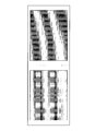
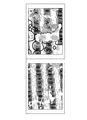
- FIG. 20 is a top view showing the state of the resist after laser irradiation by the conventional laser annealing method.
- This figure shows the results obtained after performing the laser annealing method with the energy density of the IR laser at 5.4 J / cm 2 , the overlap ratio of 67% / 50%, the pulse width of the IR laser at 20 ⁇ s, and the frequency of 1 kHz. It is.
- the lower figure shows a resist state at a magnification of 5 times
- the upper figure shows a resist state at a magnification of 50 times. As shown in FIG.
- An object of the present invention is to provide a laser annealing method for a semiconductor device, a semiconductor device, a laser annealing method, a control device for a laser annealing device, and a laser annealing device that can be used.
- a laser annealing method for a semiconductor device has the following features.
- the pulse laser beam is applied to a second region adjacent to the first region. Irradiate the beam.
- the predetermined time interval is larger than a pulse interval of the pulse laser beam.
- the laser annealing method for a semiconductor device according to the present invention is characterized in that, in the above-described invention, in the second step, the irradiation areas of the continuous pulse laser beam are separated by a predetermined interval or more.
- the predetermined interval is greater than 0% and less than or equal to 100% of a width or a height of the irradiation region.
- the predetermined interval is 1 /, / of the height of the irradiation region or the height of the irradiation region.
- the laser annealing method for a semiconductor device in the above-described invention, further comprises a step of forming a protective film on one surface of the semiconductor substrate before the second step. And irradiating the pulsed laser beam from a surface opposite to a surface on which the protective film is formed.
- a semiconductor device has the following features.
- a first semiconductor layer of the second conductivity type is provided on a front surface of the semiconductor substrate of the first conductivity type.
- a first semiconductor region of a first conductivity type is selectively provided on a surface layer of the first semiconductor layer opposite to the semiconductor substrate.
- a second semiconductor layer of a first conductivity type having a higher impurity concentration than the semiconductor substrate is selectively provided on a surface layer of the semiconductor substrate opposite to the first semiconductor layer.
- a gate electrode is provided on at least a part of a surface of the first semiconductor layer sandwiched between the first semiconductor region and the semiconductor substrate via a gate insulating film.
- a first electrode is provided on surfaces of the first semiconductor region and the first semiconductor layer.
- a second electrode is provided on a surface of the second semiconductor layer.
- the second semiconductor layer is formed by adding an impurity to the semiconductor substrate, irradiating the pulse laser beam to a first region of a part of the region to which the impurity is added, and after a predetermined time interval, Is formed by irradiating the pulse laser beam to a second region adjacent to the semiconductor substrate and annealing the semiconductor substrate.
- a laser annealing method has the following features.
- a laser annealing method for annealing the object to be annealed by repeating a unit process of scanning the surface of the object to be annealed with the pulsed laser beam a plurality of times so that the regions where the pulsed laser beam is incident do not overlap between shots.
- the surface of the object to be annealed is scanned such that a region where the pulse laser beam is incident in one of the unit steps and a region where the pulse laser beam is incident in the other one of the unit steps partially overlap.
- each of the unit steps includes a step of moving a region where the pulsed laser beam is incident at equal intervals in one direction for each shot.
- an annealing target region to be annealed is defined on the surface of the annealing target, and the light intensity has a maximum value within a beam cross section of the pulsed laser beam.
- a plurality of the unit processes are repeated so that a region where a portion of 90% or more of the incident light is incident covers the entire region to be annealed.
- a control device for a laser annealing apparatus has the following features. This is a control device of a laser annealing device that scans the surface of the object to be annealed with a pulsed laser beam.
- the control device has a function of annealing the object to be annealed by repeating a unit process of scanning the surface of the object to be annealed with the pulsed laser beam a plurality of times so that the regions where the pulsed laser beam is incident between shots do not overlap, and A function of scanning the surface of the object to be annealed such that a region where the pulsed laser beam is incident in one of the unit steps and a region where the pulsed laser beam is incident in the other one of the unit steps partially overlap with each other.
- control device of the laser annealing apparatus in the above-mentioned invention, further has a function of moving a region where a pulsed laser beam is incident at equal intervals in one direction for each shot in each of the unit processes. It is characterized by.
- an annealing target area to be annealed is defined on a surface of the annealing target, and the light intensity is within a beam cross section of the pulsed laser beam.
- a laser annealing apparatus has the following features.
- the laser annealing apparatus is a laser light source that outputs a pulsed laser beam, and the surface of the object to be annealed held at a position where the pulsed laser beam output from the laser light source is incident is irradiated with the pulsed laser beam output from the laser light source.
- a function of annealing the object to be annealed by repeating a unit process of scanning a plurality of times, and a region where a pulse laser beam is incident in one unit process and a region where a pulse laser beam is incident in another unit process And has a function of scanning the surface of the object to be annealed so that and
- the overlap ratio is smaller than 0%.
- the laser annealing method for a semiconductor device the semiconductor device, the laser annealing method, the control device of the laser annealing device, and the laser annealing device according to the present invention
- the heat generation on the non-irradiated surface side on which the protective film is provided is suppressed, thereby protecting the semiconductor device.
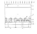
- FIG. 1 is a sectional view showing the structure of the semiconductor device according to the embodiment.
- FIG. 2 is a cross-sectional view illustrating the semiconductor device according to the embodiment during manufacture.
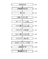
- FIG. 3 is a flowchart illustrating the method of manufacturing the semiconductor device according to the embodiment.
- FIG. 4 is a top view showing an irradiation image in the laser annealing method according to the embodiment (part 1).
- FIG. 5 is a top view showing an irradiation image in the laser annealing method according to the embodiment (part 2).
- FIG. 6 is a graph showing a laser pulse of the laser annealing apparatus according to the embodiment.
- FIG. 7A is a top view illustrating an irradiation image on a semiconductor wafer by the laser annealing method according to the embodiment (part 1).
- FIG. 7B is a top view illustrating an irradiation image on the semiconductor wafer in the laser annealing method according to the embodiment (part 2).
- FIG. 8 is a table showing the overlap rates and evaluation results of the examples and the comparative examples.
- FIG. 9 is a top view illustrating a state of the resist after laser irradiation by the laser annealing method according to the example.
- FIG. 10 is a schematic diagram illustrating a laser annealing apparatus according to the example.
- FIG. 11A is a diagram illustrating a scanning path when scanning the surface of an annealing target with a pulsed laser beam.
- FIG. 11B is a diagram showing a planar shape and a beam profile of a beam cross section.
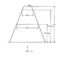
- FIG. 12 is a graph showing a beam profile in the width direction (x-axis direction) of the beam cross section.
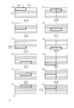
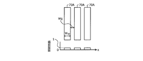
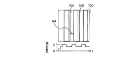
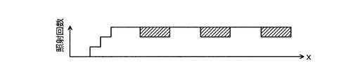
- FIG. 13A is a diagram showing a region where a pulsed laser beam is incident and a distribution of the number of irradiations in the x-axis direction in the first unit process.
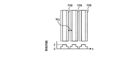
- FIG. 13B is a diagram showing, in the second unit process, a region where the pulse laser beam is incident and a distribution of the number of irradiations in the x-axis direction.
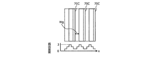
- FIG. 13C is a diagram showing, in the third unit process, the region where the pulsed laser beam is incident and the distribution of the number of irradiations in the x-axis direction.
- FIG. 13D is a diagram showing, in the fourth unit process, a region where the pulse laser beam is incident and a distribution of the number of irradiations in the x-axis direction.
- FIG. 13E is a diagram showing, in the fifth unit process, a region where the pulse laser beam is incident and a distribution of the number of irradiations in the x-axis direction.
- FIG. 14A is a diagram showing a cross-sectional structure of an annealing target by simulation.
- FIG. 14A is a diagram showing a cross-sectional structure of an annealing target by simulation.
- FIG. 14B is a graph showing the time change of the temperature in the case of three-shot irradiation.
- FIG. 15A is a table showing simulation results of the highest temperature at the positions of the upper surface, the depth of 1 ⁇ m, 2 ⁇ m, 3 ⁇ m, 4 ⁇ m, 5 ⁇ m, 10 ⁇ m, and the back surface of the object to be annealed.
- FIG. 15B is a graph showing a difference between the highest attained temperature in the case of one-shot irradiation and the highest attained temperature in the case of multiple-shot irradiation.
- FIG. 15A is a table showing simulation results of the highest temperature at the positions of the upper surface, the depth of 1 ⁇ m, 2 ⁇ m, 3 ⁇ m, 4 ⁇ m, 5 ⁇ m, 10 ⁇ m, and the back surface of the object to be annealed.
- FIG. 15B is a graph showing a difference between the highest attained temperature in the case of one-shot irradi
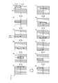
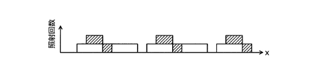
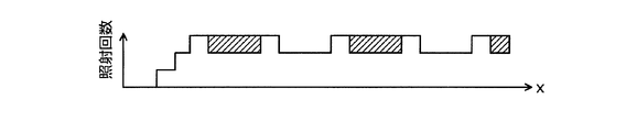
- FIG. 16A is a graph showing the distribution of the number of irradiations in the x-axis direction before and after performing the first main scan (unit process) in the annealing method according to another embodiment.
- FIG. 16B is a graph showing the distribution of the number of irradiations in the x-axis direction before and after performing the second main scan (unit process) in the annealing method according to another embodiment.
- FIG. 16C is a graph showing the distribution in the x-axis direction of the number of irradiations before and after performing the third main scan (unit process) in the annealing method according to another embodiment.
- FIG. 16A is a graph showing the distribution of the number of irradiations in the x-axis direction before and after performing the first main scan (unit process) in the annealing method according to another embodiment.
- FIG. 16B is a graph showing the distribution of the number of irradiations in the x-axis direction before and after performing the second main scan (unit
- FIG. 16D is a graph showing the distribution of the number of irradiations in the x-axis direction before and after performing the fourth main scan (unit process) in the annealing method according to another embodiment.
- FIG. 16E is a graph showing the distribution in the x-axis direction of the number of irradiations before and after performing the fifth main scan (unit process) in the annealing method according to another embodiment.
- FIG. 16F is a graph showing the distribution of the number of irradiations in the x-axis direction before and after performing the sixth main scan (unit process) in the annealing method according to another embodiment.
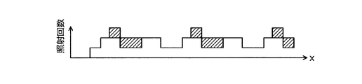
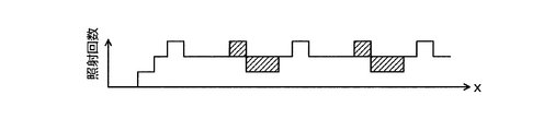
- FIG. 17A is a graph showing the distribution in the x-axis direction of the number of irradiations before and after the first main scan (unit process) in the annealing method according to still another embodiment.
- FIG. 17B is a graph showing the distribution of the number of irradiations in the x-axis direction before and after performing the second main scan (unit process) in the annealing method according to still another embodiment.
- FIG. 17C is a graph showing the distribution of the number of irradiations in the x-axis direction before and after performing the third main scan (unit process) in the annealing method according to still another embodiment.
- FIG. 17A is a graph showing the distribution in the x-axis direction of the number of irradiations before and after the first main scan (unit process) in the annealing method according to still another embodiment.
- FIG. 17B is a graph showing the distribution of the number of irradiations in the x-axis direction before and after performing the second main scan
- FIG. 17D is a graph showing the distribution of the number of irradiations in the x-axis direction before and after performing the fourth main scanning (unit process) in the annealing method according to still another embodiment.
- FIG. 17E is a graph showing the distribution of the number of irradiations in the x-axis direction before and after performing the fifth main scan (unit process) in the annealing method according to still another embodiment.
- FIG. 17F is a graph showing the distribution of the number of irradiations in the x-axis direction before and after performing the sixth main scan (unit process) in the annealing method according to still another embodiment.
- FIG. 17G is a graph showing the distribution in the x-axis direction of the number of irradiations before and after performing the seventh main scan (unit process) in the annealing method according to still another embodiment.
- FIG. 17H is a graph showing the distribution in the x-axis direction of the number of irradiations before and after performing the eighth main scan (unit process) in the annealing method according to still another embodiment.
- FIG. 18A is a plan view showing scanning lines when scanning an annealing target 40 by an annealing method according to still another embodiment.
- FIG. 18B is a diagram illustrating an example of the scanning path.
- FIG. 18C is a diagram illustrating another example of the scanning path.
- FIG. 19 is a top view showing an irradiation image in the conventional laser annealing method.
- FIG. 20 is a top view showing the state of the resist after laser irradiation by the conventional laser annealing method.
- FIG. 1 is a sectional view showing the structure of the semiconductor device according to the embodiment. Specifically, an IGBT region 12 serving as an IGBT operation region and an FWD region 13 serving as an FWD operation region are provided in parallel in an active region on the same semiconductor substrate.
- the active region is a region where a current flows when in the ON state.
- a withstand voltage structure such as a guard ring or a field plate may be provided in an edge termination region (not shown) surrounding the periphery of the active region.
- FIG. 2 is a cross-sectional view showing the semiconductor device according to the embodiment during manufacture.
- An ion implantation step (step S4) for forming an n-type field stop (FS: Field @ Stop) layer 1 on the back surface 15 side of a semiconductor wafer described later is shown.
- FS Field @ Stop
- FIG. 3 is a flowchart illustrating the method of manufacturing the semiconductor device according to the embodiment.
- FIG. 3 illustrates steps related to the laser annealing method of the present invention in detail.
- a step of forming a surface of a semiconductor device is performed (Step S1).
- an n ⁇ type semiconductor wafer to be the n ⁇ type drift region 2 is prepared.
- the material of the semiconductor wafer may be silicon (Si) or silicon carbide (SiC).
- the process of forming a set of photolithography and ion implantation is repeated under different conditions, and the p-type base region 3, n + -type emitter region 4 and p + -type of the IGBT are formed on the front surface 14 side of the semiconductor wafer.
- a contact region 5 is formed.
- P-type base region 3 is formed over the entire active region from IGBT region 12 to FWD region 13.
- the p-type base region 3 also serves as a p-type anode region in the FWD region 13.
- N + -type emitter region 4 and p + -type contact region 5 are selectively formed inside p-type base region 3 in IGBT region 12.
- the front surface 14 of the semiconductor wafer is thermally oxidized to form a field oxide film covering the front surface 14 of the semiconductor wafer in the edge termination region.
- a trench 18 is formed in the IGBT region 12 through the n + -type emitter region 4 and the p-type base region 3 to reach the n ⁇ -type drift region 2 by photolithography and etching.
- the trench 18 extends, for example, in a direction (the depth direction in FIG. 1) orthogonal to the direction in which the IGBT region 12 and the FWD region 13 are arranged (the horizontal direction in FIG. 1) when viewed from the front surface 14 side of the semiconductor wafer. They are arranged in a striped layout.
- trench 18 is formed in FWD region 13 with the same layout as IGBT region 12.
- trench 18 reaches n ⁇ -type drift region 2 through p-type base region 3 (p-type anode region).
- the gate insulating film 6 is formed along the inner wall of the trench 18 by, for example, thermal oxidation.
- a polysilicon (poly-Si) layer is formed on the front surface 14 of the semiconductor wafer so as to fill the inside of the trench 18.
- the polysilicon layer is etched back, for example, to leave a portion to be the gate electrode 8 inside the trench 18.
- n + -type emitter region 4 p + -type contact region 5
- trench 18, gate insulating film 6, and gate electrode 8 constitute a MOS gate having a trench gate structure.
- the n + -type emitter region 4 and the p + -type contact region 5 may be formed.
- the n + -type emitter region 4 only needs to be arranged in at least one mesa region between adjacent trenches 18 (mesa region), and there may be a mesa region where the n + -type emitter region 4 is not arranged.
- n + -type emitter regions 4 may be selectively arranged at predetermined intervals in a direction in which trenches 18 extend in a stripe shape.
- an interlayer insulating film 9 is formed on the front surface 14 of the semiconductor wafer so as to cover the gate electrode 8.
- the interlayer insulating film 9 is patterned to form a plurality of contact holes 28 penetrating the interlayer insulating film 9 in the depth direction.
- the depth direction is a direction from the front surface 14 to the back surface 15 of the semiconductor wafer.
- contact hole 28 of IGBT region 12 n + -type emitter region 4 and p + -type contact region 5 are exposed.
- the p-type base region 3 is exposed in the contact hole 28 of the FWD region 13.
- the surface electrode 10 is formed on the interlayer insulating film 9.
- a barrier metal film (not shown) may be formed along the inner wall of the contact hole 28, and a tungsten plug may be formed by embedding a tungsten film.
- Step S2 a step of forming the protective film 11 on the surface is performed (Step S2).
- a protective film 11 for protecting the surface of the semiconductor device with a resist, tape, glass, or the like is formed.
- the semiconductor wafer is ground from the back surface 15 side (back grinding), and a thinning step of grinding to a position of a product thickness used as a semiconductor device is performed (step S3).
- a process of forming a set of photolithography and ion implantation is repeated under different conditions, and an ion implantation process for forming an n-type field stop (FS: Field @ Stop) layer 1 on the back surface 15 side of the semiconductor wafer is performed.
- FS Field @ Stop
- FIGS. 4 and 5 are top views showing irradiation images in the laser annealing method according to the embodiment.
- FIG. 4 is an example when the overlap ratio is set to -50% / 50%
- FIG. 5 is an example when the overlap ratio is set to -100% / 50%.
- the y-axis direction is called a scan direction
- the x-axis direction is called a step direction
- the irradiation area L indicates one shot of the laser.
- each region of the semiconductor substrate is represented by a rectangle, and a specific rectangular region is represented by coordinates.
- the irradiation area L has, for example, a rectangular shape with a width (x-axis direction) of 2.5 mm and a height (y-axis direction) of 0.25 mm.
- the laser irradiates the (0, 0) region and the (0, 1) region.
- the laser moves downward in the scanning direction (positive y-axis direction), and the laser irradiates the (0, 3) area and the (0, 4) area.
- the laser does not irradiate the (0, 2) region, and the laser irradiates the region 50% higher than the region irradiated in FIG. 4A from the region irradiated in FIG. Is done.
- laser irradiation is performed by moving the region 50% lower than the irradiated region to the lower side in the scanning direction.
- the laser irradiates the (0,6) region, half of the (0,7) region, the (1,6) region, and half of the (1,7) region.
- the laser moves upward in the scanning direction (negative direction of the y-axis), and the laser is moved to the (0, 3) region, half of the (0, 4) region, and (1, 3).
- the (1, 4) area are irradiated.
- laser irradiation is performed while moving upward in the scanning direction to an area 50% higher than the irradiated area.
- the (0,0) region and half of the (0,1) region, and the (1,0) region and half of the (1,1) region at the end of the semiconductor substrate After the irradiation is performed, the laser beam is moved to the left in the step direction in order to irradiate (0, 2) regions and the like which are not overlapped or irradiated.
- the laser irradiates the (0, 1) region and the (0, 2) region.
- the laser moves downward in the scanning direction, and the laser irradiates the (0, 4) region and the (0, 5) region.
- laser irradiation is performed by moving downward from the irradiated region to a region 50% higher than this region in the scanning direction.
- FIG. 4 (i) After irradiating the (0, 7) region at the end of the semiconductor substrate, as shown in FIG. Irradiation is performed for half of the (0, 7) region and half of the (1, 7) region. Thereafter, as shown in FIG. 4 (k), the laser moves upward in the scanning direction, and the laser is moved to the (0, 4) area, half of the (0, 5) area, the (1, 4) area, and the (1, 5) area. ) Irradiate half of the area. Thereafter, similarly, as shown in FIG. 4 (l), the laser irradiation is performed while moving upward in the scanning direction from the irradiated area to an area 50% higher than the irradiated area.
- the overlap ratio is -50% / 50% because the overlap is performed 50% away from the irradiated area and 50% in the step direction.
- the first -50% is the overlap ratio in the scan direction
- the next 50% is the overlap ratio in the step direction.
- laser irradiation is performed four times on one region except for the peripheral portion.
- the laser irradiates the (0, 0) region and the (0, 1) region.
- the laser moves downward in the scanning direction (positive y-axis direction), and the laser irradiates the (0, 4) area and the (0, 5) area.
- the laser does not irradiate the (0, 2) region and the (0, 3) region, and the laser irradiates the region irradiated in FIG.
- a laser is applied to a remote area.
- the laser irradiation is performed by moving to the lower side in the scanning direction from the irradiated area to an area 100% higher than the irradiated area.
- the laser irradiates the (0,8) region, half of the (0,9) region, the (1,8) region, and half of the (1,9) region.
- the laser moves upward in the scanning direction (negative direction of the y-axis), and the laser is moved to the (0, 4) region, half of the (0, 5) region, and (1, 4). 2) Irradiation of half of the region and the (1, 5) region.
- the laser irradiation is performed by moving the region upward in the scanning direction to a region 100% apart from the irradiated region at a height of this region.
- the (0, 0) region and half of the (0, 1) region, and the (1, 0) region and half of the (1, 1) region at the end of the semiconductor substrate After the irradiation is performed, the irradiation unit moves to the left in the step direction in order to irradiate the (0, 2) region, the (0, 3) region, and the like that are not irradiated.
- the laser irradiates the (0, 2) region and the (0, 3) region.
- the laser moves downward in the scanning direction, and the laser irradiates the (0, 6) region and the (0, 7) region.
- laser irradiation is performed by moving the scanning direction downward from the irradiated area to an area 100% apart from the irradiated area.
- the laser irradiates the (0,10) region, half of the (0,11) region, and the (1,10) region and half of the (1,11) region.
- the laser moves upward in the scanning direction, and the laser emits the (0, 6) area, half of the (0, 7) area, the (1, 6) area, and the (1, 7) area.
- the laser irradiation is performed while moving upward in the scanning direction to a region 100% apart from the irradiated region at a height of this region.
- the overlap ratio is -100% / 50% because the image is overlapped by 50% in the step direction and 100% apart from the irradiated area in the scan direction.
- the first -100% is the overlap ratio in the scan direction
- the next 50% is the overlap ratio in the step direction.
- the overlap ratio is -100% / 50%, one region is irradiated with laser twice except for the peripheral portion.
- the overlap ratio in the scanning direction is preferably smaller than 0% and equal to or larger than -100% (-100% ⁇ overlap ratio ⁇ 0%).
- the region irradiated with the laser is separated from the region irradiated with the laser immediately before by a distance larger than 0% of the height of the region and 100% or less of the height of the region.
- the overlap ratio in the step direction can be other than 50%, and may be, for example, 0%.
- the step direction can be set to a minus overlap ratio.
- the overlap ratio is preferably smaller than 0% and equal to or larger than -100% (-100% ⁇ overlap ratio ⁇ 0%).
- both the step direction and the scan direction may have a negative overlap ratio.
- the overlap ratio is preferably smaller than 0% and equal to or larger than -100% (-100% ⁇ overlap ratio ⁇ 0%).
- the overlap ratio in the scanning direction By setting the overlap ratio in the scanning direction to be smaller than 0%, a time interval occurs between the irradiation of the laser to one region and the irradiation of the laser to the adjacent region, and the time for the heat of the semiconductor wafer to decrease is reduced. Occurs. Thereby, heat generation on the non-irradiation surface side can be suppressed. Therefore, when activating a deep region by IR laser annealing, the protective film is not damaged and the semiconductor device is not defective. Further, by setting it to -100% or more, it is possible to prevent a situation in which the interval between the laser irradiation regions becomes too large and the deep region cannot be sufficiently heated to be activated.
- the laser irradiation interval is a laser pulse interval.
- the laser is not continuously irradiated on an area adjacent to the scanning direction. Therefore, the time interval is larger than the laser pulse interval.
- FIG. 6 is a graph showing a laser pulse of the laser annealing apparatus according to the embodiment.
- the vertical axis indicates the intensity of the laser pulse
- the horizontal axis indicates time.
- the laser annealing apparatus generates a laser pulse L having a pulse width t2 at predetermined intervals t1.
- the laser pulse L irradiates the semiconductor wafer, moves in the scanning direction during the interval t1, and the next laser pulse L irradiates the semiconductor wafer.
- the laser pulse L is continuously irradiated in the scanning direction, but the movement in the step direction takes time. Therefore, the laser pulse L is not continuously irradiated in the step direction.
- the pulse width t2 is a half width of the laser pulse L.
- the predetermined interval t1 is, for example, 1 ms
- the pulse width t2 is, for example, 20 ⁇ s.
- a time for reducing the heat may be provided by increasing the time for the movement in the step direction.
- the end of the semiconductor wafer may be an invalid area not used for the semiconductor device. In this case, since no protective film is provided at the end, there is no problem even if the temperature rises.
- an interval can be generated between continuous laser irradiation regions even at the edge of the semiconductor wafer.
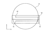
- FIGS. 7A and 7B are top views showing irradiation images on a semiconductor wafer by the laser annealing method according to the embodiment.
- FIG. 7A shows that, as shown in FIGS. 4 and 5, laser irradiation is started from the starting point S1 and moves in the scanning direction (y-axis direction) to reach the end E1 only in the step direction (x-axis direction).
- the laser beam starts moving from the start point S2, moves in the scan direction, and moves only in the step direction when reaching the end E2.
- the end portion is the end portion of the semiconductor wafer 19, and corresponds to, for example, the (0, 7) region or the (1, 7) region in FIG.
- the moving time of the laser irradiation is short, and the time for irradiating the entire surface of the semiconductor wafer with the laser can be reduced.
- FIG. 7B shows that the laser irradiation is started from the start point S1 and moves in the scan direction (y-axis direction) and moves to the step direction (x-axis direction) and the scan direction when reaching the end E1, and starts.
- Laser irradiation is started from point S2. Thereafter, when it moves in the scanning direction and reaches the end E2, it moves in the step direction and the scanning direction.
- FIG. 7B since the movement at the ends E1 and E2 moves in the scanning direction, an interval is generated between the continuous laser irradiation regions even at the ends, and the increased heat of the semiconductor wafer is also reduced at the ends. be able to.
- step S6 an ion implantation step of forming ap + -type collector region 16 on the back surface 15 side of the semiconductor wafer by photolithography and implantation of p-type ions, for example, boron (B) is performed (step S6).
- step S7 a step of forming a mask pattern having an opening in the FWD region 13 by photolithography is performed.
- an ion implantation step of forming an n + -type cathode region 17 by implanting n-type ions, for example, phosphorus (P) to change a corresponding portion to n + -type is performed (step S8).
- a step of removing the mask pattern is performed (Step S9).
- a Green laser annealing step for activating ions implanted in the p + -type collector region 16 and the n + -type cathode region 17 is performed (step S10).
- a step of removing the protective film 11 is performed (Step S11).
- the back surface electrode 7 is formed on the entire back surface 15 of the semiconductor wafer (Step S12). Back electrode 7 is in contact with p + -type collector region 16 and n + -type cathode region 17.
- the back electrode 7 functions as a collector electrode and also functions as a cathode electrode.
- the semiconductor wafer is cut (diced) into chips to be separated into individual pieces, whereby an RC-IGBT chip (semiconductor chip) is completed.
- the overlap ratio is smaller than 0%.
- there is a time interval between the irradiation of the laser in one area and the irradiation of the laser in the adjacent area which causes a time for the increased heat of the semiconductor wafer to decrease and suppresses the heat generation on the non-irradiated surface side. it can. Therefore, when activating a deep region by IR laser annealing, the protective film is not damaged and the semiconductor device is not defective.
- FIG. 8 is a table showing the overlap rates and evaluation results of the examples and the comparative examples.
- the evaluation was performed while changing the overlap ratio and the conditions of the IR laser.
- the comparative example was evaluated at a conventional overlap ratio of 67% / 50%.
- the OL rate indicates the overlap rate
- the shot number is the number of laser pulses applied to one region of the semiconductor wafer.
- the energy density, pulse width, and frequency are the conditions of the IR laser, and the units are J / cm 2 , ⁇ s, and kHz, respectively.
- the pulse width corresponds to the pulse width t2 in FIG. 6, and the frequency is the number of laser pulses per second. That is, the frequency is the reciprocal of the interval t1 in FIG.
- the activation ratio indicates the ratio of activation of ions implanted into the FS layer when the conventional example is set to 1. Peeling indicates whether the resist used as a protective film after IR laser annealing can be peeled. If the resist used as the protective film is damaged by heat, the resist is burned on the surface of the semiconductor device (semiconductor wafer) or transferred to a stage on which the semiconductor wafer is fixed during laser annealing. The evaluation result was evaluated as pass when there was no burn-in or transfer of the resist, and was rejected when there was burn-in or transfer of the resist.
- Example 2 in which the overlap ratio is 67% / 50% and in Example 1 in which the overlap ratio in the step direction is 0% and the overlap ratio in the scan direction is minus, the burn-in or transfer of the resist is performed. And the evaluation result was unacceptable. Further, in any of Examples 2 to 5 in which the overlap ratio in the step direction was plus and the overlap ratio in the scan direction was minus, no image sticking or transfer of the resist occurred, and the evaluation result was acceptable. Further, in Examples 2 to 6, the activation ratio was 0.95 to 1.00, and it can be seen that the ions implanted into the FS layer were sufficiently activated even when the overlap was negative.
- FIG. 9 is a top view illustrating a state of the resist after laser irradiation by the laser annealing method according to the example.
- This figure shows that after the laser annealing method was performed, the energy density of the IR laser was 7.5 J / cm 2 , the overlap ratio was ⁇ 50% / 50%, the pulse width of the IR laser was 20 ⁇ s, and the frequency was 1 kHz. The result.
- the lower figure shows a resist state at a magnification of 5 times
- the upper figure shows a resist state at a magnification of 50 times.
- the temperature of the surface protective film on the non-irradiated surface does not exceed the heat-resistant temperature of the protective film, so that the protective film is not damaged.
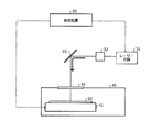
- FIG. 10 is a schematic view of a laser annealing apparatus according to the embodiment.
- the laser light source 31 outputs a pulse laser beam for annealing.
- a semiconductor laser oscillator that outputs a pulse laser beam in the infrared region can be used.
- the pulsed laser beam output from the laser light source 31 enters the annealing target 60 via the beam homogenizer 32 and the mirror 33.
- the annealing target 60 is, for example, a semiconductor wafer into which a dopant has been implanted, and performs activation anneal of the dopant by incidence of a pulsed laser beam.
- the beam homogenizer 32 shapes the beam cross-sectional shape and the beam profile of the pulse laser beam on the surface of the object 60 to be annealed.
- the beam cross section on the surface of the annealing target 60 is shaped so that the beam cross section has a long shape in one direction.
- the beam profile is shaped into a top flat shape in the length direction and width direction of the beam cross section, for example.
- the object 60 to be annealed is held on the stage 41 in the chamber 40.
- the stage 41 holds, for example, the annealing target 60 horizontally, and moves the annealing target 60 in a two-dimensional direction in a horizontal plane.
- As the stage 41 for example, an XY stage having a moving mechanism can be used.
- the pulsed laser beam is introduced into the chamber 40 through a laser transmission window 42 provided on the upper surface of the chamber 40. By moving the annealing target 60 by the stage 41, the surface of the annealing target 60 can be scanned with a pulsed laser beam.
- the controller 50 controls the output of the pulse laser beam from the laser light source 31 and the movement of the annealing target 60 by the stage 41.
- the control device 50 reads a signal from an encoder attached to the stage 41 and acquires position information of the annealing target 60. By outputting one shot of the pulse laser beam from the laser light source 31 based on the position of the object 60 to be annealed, the pulse laser beam can be incident on a target position of the object 60 to be annealed.
- the controller 50 controls the stage 41 to move the annealing target 60, and outputs a pulse laser beam from the laser light source 31 so that the pulse laser beam is incident on a target position. Thus, the region where the pulsed laser beam is incident moves on the surface of the annealing target 60 for each shot.
- the control device 50 has a function of realizing each processing of the laser annealing method described with reference to FIGS. 11A to 13E.
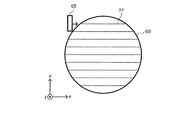
- FIG. 11A is a diagram showing a scanning path 62 of the pulse laser beam on the surface of the object 60 to be annealed.
- An xyz orthogonal coordinate system is defined in which the surface of the annealing target 60 is an xy plane and the normal direction of the surface is the z-axis direction.
- An annealing target region 61 to be annealed is defined on the surface of the substantially circular annealing target 60.
- the annealing target region 61 includes a region where the semiconductor element in the surface of the annealing target 60 is arranged. For example, a region excluding a region near the outer peripheral line of the annealing target 60 is defined as the annealing target region 61.
- the annealing target area 61 is scanned with the pulse laser beam so that the x-axis direction is the main scanning direction and the y-axis direction is the sub-scanning direction.
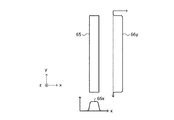
- FIG. 11B is a diagram illustrating a planar shape and a beam profile of a beam cross section 65 on the surface of the annealing target 60.
- the beam cross section 65 has a long shape that is long in one direction (y-axis direction). Both the beam profile 66x in the x-axis direction and the beam profile 66y in the y-axis direction have a top flat shape.
- the dimension in the length direction (y-axis direction) of the beam cross section 65 is about 2.5 mm
- the dimension in the width direction (x-axis direction) is about 0.3 mm.
- FIG. 12 is a graph showing a beam profile 46x in the width direction (x-axis direction) of the beam cross section 65.
- the horizontal axis in FIG. 12 represents the position in the x-axis direction, and the vertical axis represents the light intensity.
- the shape of the beam profile is approximated by an approximately isosceles trapezoid.
- the outer peripheral line of the beam cross section 65 is defined as a position where the light intensity is 50% of the maximum value IMAX .
- the width of the beam cross-section 65 is equal to the full width at half maximum W 50 of the beam profile.
- regions where the 90% value full width W 90 with less intensity unevenness is incident are arranged without gaps in the x-axis direction. It is preferable to scan the surface of the annealing target 60 with a pulsed laser beam so as to line up or partially overlap.
- annealing is performed by moving the region where the pulse beam is incident on the surface of the annealing target 60 (FIG. 11A) for each shot and causing the pulse laser beam of a plurality of shots to be incident.
- FIGS. 13A to 13E show distributions of the number of irradiations in the x-axis direction in areas 70A to 70E where the pulse laser beam is incident in the first to fifth main scans, respectively, when focusing on one main scan line.
- FIG. In the following description, attention is paid to a step of performing main scanning along one scanning line. The step of performing main scanning along other scanning lines is the same as the step described below.
- the overlap in the sub-scanning direction (y-axis direction) of the regions 70A to 70E where the pulsed laser beams are incident is not considered.
- the surface of the annealing target 60 is scanned with the pulse laser beam in the main scanning direction (x-axis) so that a gap is secured between the areas 70A where the pulse laser beam is incident.
- This scanning is performed so that the plurality of regions 70A on which the pulse laser beam is incident are arranged at equal intervals in the x-axis direction.
- the width Wg of the gap between the two regions 70A adjacent in the x-axis direction is, for example, / of the width of the beam cross section 65 (full width at half maximum W 50 ).
- the surface of the annealing target 60 is scanned so that a gap is secured between the areas where the pulsed laser beam is incident between shots. I do.
- regions 70B to 70E on which the pulsed laser beams are incident are formed by the second to fifth main scans.
- the width Wg of the gap between the regions 70B to 70E where the pulse laser beam has entered is equal to the width Wg of the gap between the regions 70A where the pulse laser beam has entered in the first main scan.
- Each of the areas 70B (FIG. 13B) where the pulse laser beam was incident in the second main scan is 67% (2/3) of the area 70A where the pulse laser beam was incident in the first main scan in the x-axis direction. Partial overlap at overlap rate. In the region where the region 70A and the region 70B overlap, the number of irradiations is two. Similarly, the regions 70C (FIG. 13C), 70D (FIG. 13D), and 70E (FIG. 13E) where the pulsed laser beam is incident in the third to fifth main scans are respectively the second to fourth times before. The areas 70B, 70C, and 70D where the pulse laser beam has entered in the main scanning partially overlap with an overlap ratio of 67%.
- a gap is secured between the areas where the pulsed laser beam is incident by two consecutive shots, so that the area where the temperature rises by the immediately preceding shot and the area where the temperature rises by the next shot are different. Do not overlap. For this reason, the influence of heat storage by the immediately preceding shot is unlikely to reach the incident area of the next shot.
- the time when the next pulse laser beam is incident so as to overlap the region where the pulse laser beam has been incident in one main scan is when the main scan is completed and the subsequent main scan is executed. For this reason, the elapsed time until the next pulse laser beam enters becomes long so as to overlap the region where one pulse laser beam enters.
- the temperature of the back surface of the annealing target 60 decreases. After the temperature of the back surface of the annealing target 60 has decreased to some extent, the next pulsed laser beam is incident, so that the temperature rise of the back surface can be suppressed.
- FIGS. 13A to 13E by performing five main scans on one main scan line, a straight line along one scan line in the annealing target area 61 (FIG. 11A) is obtained. A total of three irradiations can be performed on the region.
- the overlap ratio between the region where the pulse laser beam is incident in one main scan and the region where the pulse laser beam is incident in the next main scan is 67%.
- the area where the pulse laser beam is incident in one main scan and the area where the pulse laser beam is incident in the next main scan overlap with the area of the pulse laser beam in one main scan
- the ratio of the area of the incident area to the area is defined as the overlap ratio.
- FIG. 14A is a diagram showing a cross-sectional structure of an annealing target by simulation.
- An acrylic protective film 68 is adhered to the back surface of the annealing target 60 made of single crystal silicon.
- the protective film 68 is adsorbed on the stage 41 made of alumina (Al 2 O 3 ).
- the thickness of the object 60 to be annealed was 120 ⁇ m
- the thickness of the protective film 68 was 10 ⁇ m
- the thickness of the stage 41 was 1000 ⁇ m. It was assumed that the bottom surface of stage 41 was maintained at a temperature of 300K.
- the temperature rise when a pulsed laser beam was incident on the surface of the object 60 was determined by simulation.
- a pulse laser beam of one shot is made incident (in the case of one shot irradiation)
- a pulse laser beam of two shots is made incident on the same portion at a pulse frequency of 1 kHz (in the case of two shot irradiation)
- three pulses are made at a pulse frequency of 1 kHz.
- Simulations were performed on three types of laser irradiation when a pulsed laser beam of a shot was incident on the same location (in the case of three-shot irradiation).
- the pulse energy density on the surface of the annealing target 60 was adjusted such that the highest temperature reached the surface was about 1680K.
- the present embodiment corresponds to the case of one-shot irradiation in simulation.
- the annealing method in which scanning is performed at an overlap rate of 50% corresponds to the case of two-shot irradiation in the simulation.
- the method of scanning the surface of the annealing target 60 with the overlap ratio of 67% corresponds to the case of three-shot irradiation in the simulation.
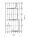
- FIG. 14B is a graph showing the time change of the temperature in the case of three-shot irradiation.
- the abscissa represents the elapsed time from the time when the first shot pulsed laser beam was incident in units of ⁇ s, and the ordinate represents the temperature in units of K.
- a thick solid line indicates a temperature change on the front surface
- a broken line indicates a temperature change at a depth of 10 ⁇ m
- a thin solid line indicates a temperature change on the back surface.
- the temperature of the front surface rises rapidly due to the incidence of the pulsed laser beam, but the temperature of the back surface rises slowly due to heat conduction from the front surface. As the laser pulse falls, the surface temperature drops rapidly. When about 200 ⁇ s elapses from the incidence of one shot of the pulsed laser beam, the temperature becomes substantially uniform from the front surface to the back surface. Thereafter, the entire temperature of the annealing target 60 gradually decreases toward 300K. When a pulsed laser beam having a pulse frequency of 1 kHz is incident, the elapsed time from the previous shot to the next shot is about 1000 ⁇ s. The temperature drop until the pulse laser beam of the next shot enters is very slight, and the temperature is kept substantially constant during a period of 1000 ⁇ s.
- the next shot enters while the heat is stored in the object 60 to be annealed, and the base temperature of the object 60 to be annealed is increased each time one shot of the pulsed laser beam is irradiated. That is, the temperature of the back surface of the annealing target 60 also gradually increases.
- FIG. 15A is a table showing simulation results of the maximum temperature at the positions of the front surface (0 ⁇ m depth), 1 ⁇ m, 2 ⁇ m, 3 ⁇ m, 4 ⁇ m, 5 ⁇ m, 10 ⁇ m, and the back surface (120 ⁇ m depth) of the annealing target 60. is there.
- the pulse energy densities for one-shot irradiation, two-shot irradiation, and three-shot irradiation were 6.8 J / cm 2 , 5.7 J / cm 2 , and 5.1 J / cm 2 , respectively. Under these conditions, the maximum temperature reached on the surface of the annealing target 60 is about 1680K. It can be seen that the higher the temperature from the surface of the object 60 to be annealed, the lower the maximum temperature.
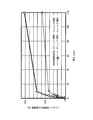
- FIG. 15B is a graph showing the difference between the highest attained temperature in the case of one shot irradiation and the highest attained temperature in the case of multiple shot irradiation.
- the second and bottom rows from the bottom of the table of FIG. 15A also show numerical values of the difference between the highest attained temperature in the case of one shot irradiation and the highest attained temperature in the case of multiple shot irradiation.
- the horizontal axis in FIG. 15B represents the depth of the annealing target 60 in the unit of “ ⁇ m”, and the vertical axis represents the difference between the maximum attained temperature in the case of one shot irradiation and the maximum attained temperature in the case of multiple shot irradiation. Represented by "K".
- the temperature difference when the maximum attained temperature in the case of multiple shot irradiation was higher than the maximum attained temperature in the case of one shot irradiation was defined as positive.
- the circle symbol in the graph of FIG. 15B indicates a difference between the highest attained temperature in the case of one-shot irradiation and the highest attained temperature in the case of two-shot irradiation. 3 shows the difference from the highest attained temperature in the case of three shot irradiation.
- the difference in the highest temperature between the case of single shot irradiation and the case of multiple shot irradiation is at most 70K.
- the difference between the maximum attained temperatures in the case of one-shot irradiation and the case of two-shot irradiation exceeds 100 K, and the difference between the maximum attained temperatures of one-shot irradiation and three-shot irradiation is Over 200K.
- the overlap ratio between the region where the pulse laser beam is incident in the immediately preceding main scan and the region where the pulse laser beam is incident in the next main scan is 67%.
- 2/3 has been described, another overlap ratio may be used.
- the overlap ratio between the region where the pulse laser beam is incident in the immediately preceding main scan and the region where the pulse laser beam is incident in the next main scan may be set to 50%.
- the calculation of the overlap ratio of the area where the pulse laser beam is incident in the two different main scans is performed based on the area where the pulse laser beam is incident in the immediately preceding main scan, instead of using the area where the pulse laser beam is incident in the previous main scan.
- the region where the pulse laser beam is incident in the scanning may be used as a reference.
- the execution order of the five main scans from FIG. 13A to FIG. 13E may be changed.
- the area where the inside portion of the 90% value full width W 90 (FIG. 12) of the beam profile is incident without any gap in the x-axis direction is incident without any gap in the x-axis direction. Or, it is preferable that they are arranged so as to overlap.
- the region where the pulsed laser beam is incident is moved at equal intervals in the x-axis direction for each shot, but may be moved at irregular intervals. Even when moving at unequal intervals, when all of the main scanning is completed, a region where 90% value inside portion of the total width W 90 of the beam profile incident are aligned with no gap or overlap, in the x-axis direction It is good to do.
- the areas where the pulsed laser beams are incident do not overlap between shots.
- the step of scanning the surface of the object to be annealed with the pulsed laser beam so that the regions where the pulsed laser beam is incident does not overlap between shots is referred to as a “unit step”.
- the unit process is not limited to one main scan.
- the process of repeating the main scanning and the sub-scanning can be regarded as one unit process.
- the starting point and the ending point for scanning in one unit process may be arbitrarily set.
- one annealing target area 61 may be divided in the y-axis direction to define a plurality of sections, and the unit process may be repeated for each section.
- FIGS. 16A to 16F a laser annealing method according to another embodiment will be described with reference to FIGS. 16A to 16F.
- description of the configuration common to the laser annealing method according to the embodiment shown in FIGS. 10 to 15B will be omitted.
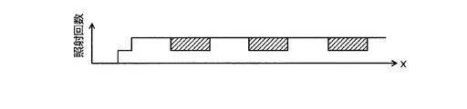
- FIGS. 16A to 16F are graphs showing the distribution of the number of irradiations in the x-axis direction before and after performing the first to sixth main scans (unit processes), respectively.
- the horizontal axis represents the position in the x-axis direction
- the vertical axis represents the number of irradiations.
- the number of irradiations before the main scanning corresponding to the graph is represented by a thick solid line
- the increment of the number of irradiations by the main scanning corresponding to the graph is indicated by a hatched area 75.
- the hatched area 75 indicates an area in the x-axis direction where the pulse laser beam is irradiated by one main scan corresponding to the graph.
- the surface of the annealing target 60 (FIG. 11A) is scanned so that the areas where the pulsed laser beams are incident do not overlap each other.
- the pulse laser beam enters between the regions where the pulse laser beam has entered in the first main scan (FIG. 16A), and the incident regions of both pulse laser beams overlap each other. No.
- the surface of the annealing target 60 is irradiated with the pulse laser beam in the main scan direction (x-axis direction).
- the surface of the annealing target 60 is scanned such that the overlap ratio with respect to the region where the pulse laser beam is incident in the first main scan (FIG. 16A) is 67%.
- the overlap ratio with respect to the area where the pulse laser beam is incident in the two main scans becomes 67%.
- the surface of the object 60 to be annealed is scanned so as to be as follows.
- the regions where the pulsed laser beams enter may not overlap.
- FIGS. 17A to 17H a laser annealing method according to still another embodiment will be described with reference to FIGS. 17A to 17H.
- description of the configuration common to the laser annealing method according to the embodiment shown in FIGS. 10 to 15B will be omitted.
- FIGS. 17A to 17H are graphs showing the distribution of the number of irradiations in the x-axis direction before and after performing the first to eighth main scans (unit processes), respectively.
- the horizontal axis represents the position in the x-axis direction
- the vertical axis represents the number of irradiations.
- the number of irradiations before the main scan corresponding to the graph is represented by a thick solid line
- the increase in the number of irradiations by the main scan corresponding to the graph is indicated by a hatched area 75.
- the hatched area 75 indicates an area in the x-axis direction where the pulse laser beam is irradiated by one main scan corresponding to the graph.
- the interval between the areas where the pulse laser beams are incident in each of the main scans is wider than that in the embodiment shown in FIGS. 16A to 16F. Therefore, the region where the pulse laser beam is incident in the second main scan (FIG. 17B) is separated from the region where the pulse laser beam is incident in the first main scan (FIG. 17A).
- the surface of the annealing target 60 is scanned such that the overlap ratio with respect to the region where the pulse laser beam is incident in the first main scan (FIG. 17A) is 67%.
- the region where the pulse laser beam is incident in the third main scan (FIG. 17C) does not overlap with the region where the pulse laser beam is incident in the second main scan (FIG. 17B) and is in contact.
- the overlap ratio with respect to the area where the pulsed laser beam is incident in the two main scans becomes 67%.
- the surface of the object 60 to be annealed is scanned so as to be as follows. Further, the region where the pulse laser beam enters in the fourth to eighth main scans (FIGS. 17D to 17H) does not overlap with the region where the pulse laser beam enters in the immediately preceding main scan (FIGS. 17C to 17G). .
- the region where the pulsed laser beam is incident does not overlap with the region where the pulsed laser beam was incident in the immediately preceding main scan, and the region where the pulsed laser beam was incident in the main scan several times earlier. You may make it overlap.
- FIGS. 18A to 18C a laser annealing method according to still another embodiment will be described with reference to FIGS. 18A to 18C.
- description of the configuration common to the laser annealing method according to the embodiment shown in FIGS. 10 to 15B will be omitted.
- FIG. 18A is a plan view showing a scanning line 77 when scanning the object 60 to be annealed.
- the main scanning direction is parallel to the x-axis.
- the center of the beam section 65 of the pulse laser beam moves so as to follow the scanning line 77.
- the overlap ratio in the sub-scanning direction is 50%
- the interval between the scanning lines 77 is ⁇ of the dimension (length) of the beam cross section 65 in the y-axis direction.
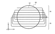
- FIG. 18B is a diagram illustrating an example of the scanning path 62.
- FIG. 18C is a diagram showing another example of the scanning path 62.
- the surface of the annealing target 60 is divided into two partial regions 78. After scanning one scanning line 77 in one partial area 78, one scanning line 77 in the other partial area 78 is scanned. As described above, the scanning lines 77 may be alternately selected from the two partial regions 78, and the selected scanning lines 77 may be sequentially scanned.
- sub-scanning is performed so that the areas where the pulsed laser beams are incident do not overlap in the sub-scanning direction. Therefore, the influence of heat before and after the sub scanning can be reduced.
- the annealing target 60 is moved with respect to the path of the pulsed laser beam, but the path of the pulsed laser beam may be moved with respect to the annealing target 60. That is, the path of the pulsed laser beam may be shifted in a two-dimensional direction.
- a scanning mechanism for moving one of the path of the pulsed laser beam and the annealing target 60 with respect to the other may be provided.
- the present invention can be variously modified without departing from the gist of the present invention.
- the size of each part, the impurity concentration, and the like are variously set according to required specifications and the like.
- the first conductivity type is n-type and the second conductivity type is p-type.
- the present invention is similarly applicable to a case where the first conductivity type is p-type and the second conductivity type is n-type. Holds.
- the laser annealing method for a semiconductor device, the semiconductor device, the laser annealing method, the control device of the laser annealing device, and the laser annealing device according to the present invention can be applied to power supply devices and power supply devices for various industrial machines. It is useful for manufacturing a power semiconductor device to be used.
- Reference Signs List 1 n-type FS layer 2 n - type drift region 3 p-type base region 4 n + type emitter region 5 p + type contact region 6 gate insulating film 7 back electrode 8 gate electrode 9 interlayer insulating film 10 surface electrode 11 protective film 12 IGBT Region 13 FWD region 16 p + type collector region 17 n + type cathode region 18 trench 19 semiconductor wafer 28 contact hole 31 laser light source 32 beam homogenizer 33 mirror 40 chamber 41 stage 42 laser transmission window 50 control device 60 annealing target 61 annealing target Region 62 Scanning path 65 Beam cross section 66x Beam profile in x-axis direction 66y Beam profile in y-axis direction 68 Protective films 70A, 70B, 70C, 70D, 70E Region 75 where pulsed laser beam is incident Number of irradiation times by one main scan Area indicating increment Area 77 Scan line 78 Partial area
Landscapes
- Physics & Mathematics (AREA)
- Optics & Photonics (AREA)
- Engineering & Computer Science (AREA)
- Plasma & Fusion (AREA)
- Mechanical Engineering (AREA)
- Recrystallisation Techniques (AREA)
- Electromagnetism (AREA)
Abstract
半導体装置のレーザーアニール方法は、半導体基板に不純物を添加する第1工程と、不純物が添加された領域に、複数回パルスレーザービームを照射して半導体基板のアニールを行う第2工程と、を含む。第2工程では、不純物が添加された領域の一部の第1領域にパルスレーザービームを照射した後、所定の時間間隔後、第1領域と隣接する第2領域にパルスレーザービームを照射する。所定の時間間隔は、パルスレーザービームのパルス間隔より大きい。
Description
この発明は、半導体装置のレーザーアニール方法、半導体装置、レーザーアニール方法、レーザーアニール装置の制御装置およびレーザーアニール装置に関する。
従来、半導体装置を作製(製造)する際に、半導体基板(半導体ウエハ)に形成されるイオン注入層の活性化を目的とするアニール熱処理を、レーザー照射エネルギーによる温度上昇を利用したレーザーアニール処理により行っている。
また、深い領域に注入されたイオンを活性化するため、赤外線領域の波長(例えば、808nm)を利用した赤外(IR:infrared)レーザーアニールが行われている。1回のレーザー照射で半導体基板の全面に照射できないため、複数のショットを繰り返し行っている。この際、レーザーアニール装置に、オーバーラップ率を設定して、レーザーの1ショットを少しずつずらして連続的に同じ箇所に複数回レーザー照射を行っている。
図19は、従来のレーザーアニール方法における照射イメージを示す上面図である。図19はオーバーラップ率を50%/50%に設定した場合の例である。オーバーラップ率とは、スキャン方向(y軸方向)に照射領域を重ね合わせ(オーバーラップ)する割合と、ステップ方向に(x軸方向)に照射領域を重ね合わせする割合とを示すレーザーアニール装置の主要なパラメータである。50%/50%の場合、スキャン方向に50%重ね合わせし、ステップ方向に50%重ね合わせする。ここで最初の50%がスキャン方向のオーバーラップ率であり、次の50%がステップ方向のオーバーラップ率である。
図19において、y軸方向は、スキャン方向と呼ばれ、x軸方向はステップ方向と呼ばれる。図19で照射領域Lがレーザーの1ショットを示す。また、図19では半導体基板の各領域を矩形で示しており、以下特定の矩形の領域を座標で示す。例えば、図19で最も左側(x軸の負の方向)で、最も上側(y軸の負の方向)の領域は(0、0)領域と表し、(0、0)領域の右側(x軸の正の方向)を(1、0)領域と表し、(0、0)領域の下側(y軸の正の方向)を(0、1)領域と表す。
最初に、図19(a)に示すように、レーザーは(0、0)領域と(0、1)領域を照射する。次に、図19(b)に示すように、スキャン方向下側(y軸正の方向)に移動して、レーザーは(0、1)領域と(0、2)領域を照射する。このように、図19(a)で照射した領域の50%が再度照射される。この後同様に、図19(c)~図19(f)に示すように照射した領域の50%を再度照射するようにして、スキャン方向下側に移動してレーザーの照射を行う。
次に、図19(f)のように半導体基板の端部の(0、5)領域と(0、6)領域の照射を行ったら、図19(g)に示すように、ステップ方向右側(x軸正の方向)に移動して、レーザーは(0、5)領域と(0、6)領域の半分と(1、5)領域と(1、6)領域の半分の照射を行う。この後、図19(h)に示すように、スキャン方向上側(y軸負の方向)に移動して、レーザーは(0、4)領域と(0、5)領域の半分と(1、4)領域と(1、5)領域の半分の照射を行う。この後同様に、図19(i)~図19(l)に示すように照射した領域の50%を再度照射するようにして、スキャン方向にレーザーの照射を行う。
このように、スキャン方向に50%重ね合わせし、ステップ方向に50%重ね合わせすることで、50%/50%のオーバーラップ率では、レーザー照射を行う領域の外周の部分を除いて、1つの領域に4回のレーザー照射が行われる。
オーバーラップ率は、このほかに67%/50%や67%/67%などに設定することも可能である。67%の場合は、2/3の部分がオーバーラップすることになり、1つの領域に照射されるレーザーの回数が増えていく。例えば、オーバーラップ率67%/50%の場合、レーザー照射を行う領域の外周の部分を除いて、1つの領域に6回のレーザー照射が行われる。
このように、連続的に同じ箇所に複数回レーザー照射を行うことで、対象の温度が高まり、半導体基板内に熱が蓄積していき、イオン注入にした不純物の活性化が促進される。これにより、イオン注入で生じた結晶欠陥が回復し、また、不純物の活性化によりn型またはp型の活性層が形成される。
また、高品質のアニールを行うため、入射順序が連続する任意の2つのレーザーパルスの入射領域が重複部分をもたないように、不純物が添加された半導体基板に複数のレーザーパルスを入射させるレーザーアニール方法が公知である(下記、特許文献1参照)。
また、IGBT(Insulated Gate Bipolar Transistor:絶縁ゲート型バイポーラトランジスタ)などの不純物活性化を十分な深さまで効果的に行うことを可能にするレーザーアニール方法が公知である(下記、特許文献2参照)。このレーザーアニール方法では、パルス波形の最大強度の10%から90%にまで到達する立ち上がり時間が160ns以上で、立ち上がり時間とパルス波形の最大強度の90%から10%にまで到達する立ち下がり時間との比が1より大きいレーザーパルスを用いる。このレーザーパルスを走査しながら半導体ウエハに繰り返し重複照射し、半導体ウエハが非溶融で処理層が非溶解状態を維持し、または表層のみが溶融して表層を除く処理層が非溶解状態を維持するようにして半導体ウエハの熱処理を行う。この方法では、パルスレーザーの光侵入長を長くでき、目標とする深い領域(例えば2μm以上)まで活性化が可能となる。
しかしながら、深い領域のイオンを活性化させる赤外レーザー(以下、IRレーザーとする)は、エネルギー密度が高く設定される。例えば、表面領域のイオンを活性化させるグリーン(Green)レーザーより3~6倍程度エネルギー密度が高く設定される。このため、シリコン(Si)結晶の発熱が大きく、レーザー照射により半導体ウエハの照射面に発生した熱が、反対側の非照射面まで伝わり、非照射面の温度が上昇してしまう。通常、半導体ウエハの非照射面に素子構造が形成されており、素子構造を保護するために保護テープ等の保護膜が非照射面に貼り付けられている。
この保護膜及び接着剤には、通常、200℃~300℃程度の耐熱性しかない。非照射面が耐熱温度以上まで上昇すると、保護膜に発泡や変質が生じる場合がある。その結果、保護膜の除去工程で保護膜を半導体ウエハから除去し難くなってしまう。また、保護膜の損傷が生じ、例えば、保護膜がレジストであれば、レジストの焼き付き、ステージ側へのレジストの転写等が生じる。保護膜がテープやガラス補強であれば、補強剤の変質、変形や接着剤(糊)の残渣が懸念される。
図20は、従来のレーザーアニール方法でレーザー照射後のレジストの状態を示す上面図である。この図は、IRレーザーのエネルギー密度を5.4J/cm2、オーバーラップ率を67%/50%、IRレーザーのパルス幅を20μs、周波数を1kHzにして、レーザーアニール方法を行った後の結果である。図20において、下図は倍率5倍のレジスト状態を示し、上図は倍率50倍のレジスト状態を示す。図20に示すように従来のレーザーアニール方法では、非照射面の表面保護膜までに熱が伝わり温度が上昇し保護膜の耐熱温度を超え、保護膜に損傷が発生している。保護膜の損傷により、半導体装置の表面を保護できず、半導体装置の製造を進めることができなくなり、不良品となってしまう。
この発明は、上述した従来技術による問題点を解消するため、保護膜が設けられた非照射面側の発熱を抑えることで、保護膜を損傷させず、照射面側の表層部を十分アニールすることができる半導体装置のレーザーアニール方法、半導体装置、レーザーアニール方法、レーザーアニール装置の制御装置およびレーザーアニール装置を提供することを目的とする。
上述した課題を解決し、本発明の目的を達成するため、この発明にかかる半導体装置のレーザーアニール方法は、次の特徴を有する。半導体基板に不純物を添加する第1工程と、前記不純物が添加された領域に、複数回パルスレーザービームを照射して前記半導体基板のアニールを行う第2工程と、を含む。前記第2工程では、前記不純物が添加された領域の一部の第1領域に前記パルスレーザービームを照射した後、所定の時間間隔後、前記第1領域と隣接する第2領域に前記パルスレーザービームを照射する。
また、この発明にかかる半導体装置のレーザーアニール方法は、上述した発明において、前記所定の時間間隔は、前記パルスレーザービームのパルス間隔より大きいことを特徴とする。
また、この発明にかかる半導体装置のレーザーアニール方法は、上述した発明において、前記第2工程では、連続する前記パルスレーザービームの照射領域間が所定の間隔以上離れていることを特徴とする。
また、この発明にかかる半導体装置のレーザーアニール方法は、上述した発明において、前記所定の間隔は、前記照射領域の幅または高さの0%より大きく、100%以下であることを特徴とする。
また、この発明にかかる半導体装置のレーザーアニール方法は、上述した発明において、前記所定の間隔は、前記照射領域の高さの1/2、2/3または前記照射領域の高さであることを特徴とする。
また、この発明にかかる半導体装置のレーザーアニール方法は、上述した発明において、前記第2工程より前に、前記半導体基板の一方の面に保護膜を形成する工程をさらに含み、前記第2工程では、前記保護膜が形成された面と反対側の面から前記パルスレーザービームを照射することを特徴とする。
上述した課題を解決し、本発明の目的を達成するため、この発明にかかる半導体装置は、次の特徴を有する。第1導電型の半導体基板のおもて面に第2導電型の第1半導体層が設けられる。前記第1半導体層の、前記半導体基板側に対して反対側の表面層に選択的に第1導電型の第1半導体領域が設けられる。前記半導体基板の、前記第1半導体層に対して反対側の表面層に選択的に、前記半導体基板より高不純物濃度の第1導電型の第2半導体層が設けられる。前記第1半導体領域と前記半導体基板とに挟まれた前記第1半導体層の表面上の少なくとも一部にゲート絶縁膜を介してゲート電極が設けられる。前記第1半導体領域と前記第1半導体層の表面に第1電極が設けられる。前記第2半導体層の表面に第2電極が設けられる。前記第2半導体層は、前記半導体基板に不純物を添加し、前記不純物が添加された領域の一部の第1領域に前記パルスレーザービームを照射した後、所定の時間間隔後、前記第1領域と隣接する第2領域に前記パルスレーザービームを照射して、前記半導体基板のアニールを行うことで形成される。
上述した課題を解決し、本発明の目的を達成するため、この発明にかかるレーザーアニール方法は、次の特徴を有する。ショット間でパルスレーザービームが入射する領域が重ならないように、パルスレーザービームでアニール対象物の表面を走査する単位工程を複数回繰り返して前記アニール対象物をアニールするレーザーアニール方法であって、1つの前記単位工程でパルスレーザービームが入射する領域と、他の1つの前記単位工程でパルスレーザービームが入射する領域とが部分的に重なるように、前記アニール対象物の表面を走査する。
また、この発明にかかるレーザーアニール方法は、上述した発明において、前記単位工程の各々は、パルスレーザービームの入射する領域をショットごとに一方向に等間隔で移動させる工程を含むことを特徴とする。
また、この発明にかかるレーザーアニール方法は、上述した発明において、前記アニール対象物の表面に、アニールすべきアニール対象領域が画定されており、パルスレーザービームのビーム断面内において、光強度が最大値の90%以上となる部分が入射した領域が、前記アニール対象領域を隈なく覆うように、複数の前記単位工程を繰り返すことを特徴とする。
上述した課題を解決し、本発明の目的を達成するため、この発明にかかるレーザーアニール装置の制御装置は、次の特徴を有する。パルスレーザービームでアニール対象物の表面を走査するレーザーアニール装置の制御装置である。制御装置は、ショット間でパルスレーザービームが入射する領域が重ならないように、パルスレーザービームで前記アニール対象物の表面を走査する単位工程を複数回繰り返して前記アニール対象物をアニールする機能、及び1つの前記単位工程でパルスレーザービームが入射する領域と、他の1つの前記単位工程でパルスレーザービームが入射する領域とが部分的に重なるように、前記アニール対象物の表面を走査する機能を有する。
また、この発明にかかるレーザーアニール装置の制御装置は、上述した発明において、前記単位工程の各々において、パルスレーザービームの入射する領域をショットごとに一方向に等間隔で移動させる機能をさらに有することを特徴とする。
また、この発明にかかるレーザーアニール装置の制御装置は、上述した発明において、前記アニール対象物の表面に、アニールすべきアニール対象領域が画定されており、パルスレーザービームのビーム断面内において、光強度が最大値の90%以上となる部分が入射した領域が、前記アニール対象領域を隈なく覆うように、複数の前記単位工程を繰り返す機能を、さらに有することを特徴とする。
上述した課題を解決し、本発明の目的を達成するため、この発明にかかるレーザーアニール装置は、次の特徴を有する。レーザーアニール装置は、パルスレーザービームを出力するレーザー光源と、前記レーザー光源から出力されたパルスレーザービームが入射する位置に保持されたアニール対象物の表面を前記レーザー光源から出力されたパルスレーザービームで走査する走査機構と、前記レーザー光源及び前記走査機構を制御する制御装置とを有する。前記制御装置は、前記レーザー光源及び前記走査機構を制御して、前記レーザー光源から出力されたパルスレーザービームで、ショット間でパルスレーザービームが入射する領域が重ならないように前記アニール対象物の表面を走査する単位工程を複数回繰り返して前記アニール対象物をアニールする機能、及び1つの前記単位工程でパルスレーザービームが入射する領域と、他の1つの前記単位工程でパルスレーザービームが入射する領域とが部分的に重なるように、前記アニール対象物の表面を走査する機能を有する。
上述した発明によれば、半導体装置のレーザーアニール方法は、オーバーラップ率を0%より小さくしている。これにより、レーザーがある領域に照射された後、隣接する領域へのレーザー照射までに時間間隔が生じ、半導体ウエハの上昇した熱が下がる時間を生じさせ、非照射面側の発熱を抑えることができる。このため、IRレーザーアニールによる深い領域の活性化の際に、保護膜を損傷することなく、半導体装置を不良とすることがない。
本発明にかかる半導体装置のレーザーアニール方法、半導体装置、レーザーアニール方法、レーザーアニール装置の制御装置およびレーザーアニール装置によれば、保護膜が設けられた非照射面側の発熱を抑えることで、保護膜を損傷させず、照射面側の表層部を十分アニールすることができるという効果を奏する。
以下に添付図面を参照して、この発明にかかる半導体装置のレーザーアニール方法、半導体装置、レーザーアニール装置の制御装置およびレーザーアニール装置の好適な実施の形態を詳細に説明する。本明細書および添付図面においては、nまたはpを冠記した層や領域では、それぞれ電子または正孔が多数キャリアであることを意味する。また、nやpに付す+および-は、それぞれそれが付されていない層や領域よりも高不純物濃度および低不純物濃度であることを意味する。なお、以下の実施の形態の説明および添付図面において、同様の構成には同一の符号を付し、重複する説明を省略する。
(実施の形態)
実施の形態にかかる半導体装置のレーザーアニール方法について、半導体装置として逆導通型IGBT(RC-IGBT)を製造する方法を例に説明する。RC-IGBTは、例えばトレンチゲート構造のIGBTと、このIGBTに逆並列に接続したFWD(Free Wheeling Diode:還流ダイオード)とを同一の半導体基板(半導体チップ)上に一体化してなる。図1は、実施の形態にかかる半導体装置の構造を示す断面図である。具体的には、同一の半導体基板上の活性領域に、IGBTの動作領域となるIGBT領域12と、FWDの動作領域となるFWD領域13とが並列に設けられている。活性領域は、オン状態のときに電流が流れる領域である。活性領域の周囲を囲むエッジ終端領域(不図示)にガードリングやフィールドプレート等の耐圧構造が設けられていてもよい。
実施の形態にかかる半導体装置のレーザーアニール方法について、半導体装置として逆導通型IGBT(RC-IGBT)を製造する方法を例に説明する。RC-IGBTは、例えばトレンチゲート構造のIGBTと、このIGBTに逆並列に接続したFWD(Free Wheeling Diode:還流ダイオード)とを同一の半導体基板(半導体チップ)上に一体化してなる。図1は、実施の形態にかかる半導体装置の構造を示す断面図である。具体的には、同一の半導体基板上の活性領域に、IGBTの動作領域となるIGBT領域12と、FWDの動作領域となるFWD領域13とが並列に設けられている。活性領域は、オン状態のときに電流が流れる領域である。活性領域の周囲を囲むエッジ終端領域(不図示)にガードリングやフィールドプレート等の耐圧構造が設けられていてもよい。
図2は、実施の形態に係る半導体装置の製造途中を示す断面図である。後述する半導体ウエハの裏面15側に、n型フィールドストップ(FS:Field Stop)層1を形成するためのイオン注入工程(ステップS4)を示している。
図3は、実施の形態にかかる半導体装置の製造方法を示すフローチャートである。図3では、本発明のレーザーアニール方法に関する工程を詳しく記載している。まず、半導体装置の表面を形成する工程を行う(ステップS1)。この工程では、まず、n-型ドリフト領域2となるn-型の半導体ウエハを用意する。半導体ウエハの材料は、シリコン(Si)であってもよいし、炭化珪素(SiC)であってもよい。次に、フォトリソグラフィおよびイオン注入を1組とする工程を異なる条件で繰り返し行い、半導体ウエハのおもて面14側に、IGBTのp型ベース領域3、n+型エミッタ領域4およびp+型コンタクト領域5を形成する。p型ベース領域3は、IGBT領域12からFWD領域13にわたって活性領域全面に形成される。p型ベース領域3は、FWD領域13においてp型アノード領域を兼ねる。n+型エミッタ領域4およびp+型コンタクト領域5は、IGBT領域12においてp型ベース領域3の内部に選択的に形成される。
次に、半導体ウエハのおもて面14を熱酸化して、エッジ終端領域において半導体ウエハのおもて面14を覆うフィールド酸化膜を形成する。次に、フォトリソグラフィおよびエッチングにより、IGBT領域12においてn+型エミッタ領域4およびp型ベース領域3を貫通してn-型ドリフト領域2に達するトレンチ18を形成する。トレンチ18は、半導体ウエハのおもて面14側から見て、例えば、IGBT領域12とFWD領域13とが並ぶ方向(図1の横方向)と直交する方向(図1の奥行き方向)に延びるストライプ状のレイアウトに配置されている。
また、トレンチ18は、IGBT領域12と同様のレイアウトで、FWD領域13にも形成される。FWD領域13において、トレンチ18は、p型ベース領域3(p型アノード領域)を貫通してn-型ドリフト領域2に達する。次に、例えば熱酸化により、トレンチ18の内壁に沿ってゲート絶縁膜6を形成する。次に、半導体ウエハのおもて面14上に、トレンチ18の内部を埋め込むようにポリシリコン(poly-Si)層を形成する。次に、このポリシリコン層を例えばエッチバックして、ゲート電極8となる部分をトレンチ18の内部に残す。
これらのp型ベース領域3、n+型エミッタ領域4、p+型コンタクト領域5、トレンチ18、ゲート絶縁膜6およびゲート電極8でトレンチゲート構造のMOSゲートが構成される。ゲート電極8の形成後に、n+型エミッタ領域4およびp+型コンタクト領域5を形成してもよい。n+型エミッタ領域4は、隣り合うトレンチ18間(メサ領域)の少なくとも1つのメサ領域に配置されていればよく、n+型エミッタ領域4を配置しないメサ領域が存在してもよい。また、n+型エミッタ領域4は、トレンチ18がストライプ状に延びる方向に所定の間隔で選択的に配置されていてもよい。
次に、半導体ウエハのおもて面14上に、ゲート電極8を覆うように層間絶縁膜9を形成する。次に、層間絶縁膜9をパターニングして、層間絶縁膜9を深さ方向に貫通する複数のコンタクトホール28を形成する。深さ方向とは、半導体ウエハのおもて面14から裏面15に向かう方向である。IGBT領域12のコンタクトホール28には、n+型エミッタ領域4およびp+型コンタクト領域5が露出される。FWD領域13のコンタクトホール28には、p型ベース領域3が露出される。
次に、層間絶縁膜9の上部に表面電極10を形成する。なお、コンタクトホール28の内壁に沿うようにバリアメタル膜(不図示)を形成し、タングステン膜を埋め込んでタングステンプラグ(不図示)を形成してもよい。
次に、表面に保護膜11を形成する工程を行う(ステップS2)。表面電極10上に、例えば、レジスト、テープ、ガラス等で半導体装置の表面を保護する保護膜11を形成する。次に、半導体ウエハを裏面15側から研削していき(バックグラインド)、半導体装置として用いる製品厚さの位置まで研削する薄化工程を行う(ステップS3)。次に、フォトリソグラフィおよびイオン注入を1組とする工程を異なる条件で繰り返し行い、半導体ウエハの裏面15側に、n型フィールドストップ(FS:Field Stop)層1を形成するためのイオン注入工程を行う(ステップS4)。例えば、図2の矢印Aのように、n型のイオン、例えばリン(P)を注入する。
次に、n型FS層に注入したイオンを活性化させるIRレーザーアニール工程を行う(ステップS5)。ここで、図4、図5は、実施の形態にかかるレーザーアニール方法における照射イメージを示す上面図である。図4は、オーバーラップ率を-50%/50%に設定した場合の例であり、図5は、オーバーラップ率を-100%/50%に設定した場合の例である。図4、図5においても、y軸方向は、スキャン方向と呼ばれ、x軸方向はステップ方向と呼ばれ、照射領域Lがレーザーの1ショットを示す。また、図4、図5でも、半導体基板の各領域を矩形で示しており、特定の矩形の領域を座標で表す。実施の形態において、照射領域Lは、例えば、幅(x軸方向)2.5mm、高さ(y軸方向)0.25mmの矩形の形状である。
最初に、図4のオーバーラップ率-50%/50%の場合を説明する。まず、図4(a)に示すように、レーザーは(0、0)領域と(0、1)領域を照射する。次に、図4(b)に示すように、スキャン方向下側(y軸正の方向)に移動して、レーザーは(0、3)領域と(0、4)領域を照射する。このように、レーザーは(0、2)領域の照射を行わず、図4(a)で照射した領域から、図4(a)で照射した領域の高さ50%離れた領域にレーザーが照射される。この後同様に、図4(c)に示すように照射した領域から、この領域の高さ50%離れた領域に、スキャン方向下側に移動してレーザーの照射を行う。
次に、図4(c)のように半導体基板の端部の(0、6)領域と(0、7)領域の照射を行ったら、図4(d)に示すように、ステップ方向右側(x軸正の方向)に移動して、レーザーは(0、6)領域と(0、7)領域の半分と(1、6)領域と(1、7)領域の半分の照射を行う。この後、図4(e)に示すように、スキャン方向上側(y軸負の方向)に移動して、レーザーは(0、3)領域と(0、4)領域の半分と(1、3)領域と(1、4)領域の半分の照射を行う。この後同様に、図4(f)に示すように照射した領域から、この領域の高さ50%離れた領域に、スキャン方向上側に移動してレーザーの照射を行う。
次に、図4(f)のように半導体基板の端部の(0、0)領域と(0、1)領域の半分と、(1、0)領域と(1、1)領域の半分の照射を行ったら、重ね合わせおよび照射されていない(0、2)領域等の照射を行うため、ステップ方向左側に移動する。図4(g)に示すように、レーザーは(0、1)領域と(0、2)領域の照射を行う。この後、図4(h)に示すように、スキャン方向下側に移動して、レーザーは(0、4)領域と(0、5)領域の照射を行う。この後同様に、図4(i)に示すように照射した領域から、この領域の高さ50%離れた領域に、スキャン方向下側に移動してレーザーの照射を行う。
次に、図4(i)のように半導体基板の端部の(0、7)領域の照射を行ったら、図4(j)に示すように、ステップ方向右側に移動して、レーザーは(0、7)領域の半分と(1、7)領域の半分の照射を行う。この後、図4(k)に示すように、スキャン方向上側に移動して、レーザーは(0、4)領域と(0、5)領域の半分と(1、4)領域と(1、5)領域の半分の照射を行う。この後同様に、図4(l)に示すように照射した領域から、この領域の高さ50%離れた領域に、スキャン方向上側に移動してレーザーの照射を行う。
このように、スキャン方向に、照射した領域から50%離し、ステップ方向に50%重ね合わせするため、オーバーラップ率は-50%/50%となる。ここで最初の-50%がスキャン方向のオーバーラップ率であり、次の50%がステップ方向のオーバーラップ率である。オーバーラップ率-50%/50%の場合、周辺の部分を除いて、1つの領域に4回のレーザー照射が行われる。
次に、図5のオーバーラップ率-100%/50%の場合を説明する。まず、図5(a)に示すように、レーザーは(0、0)領域と(0、1)領域を照射する。次に、図5(b)に示すように、スキャン方向下側(y軸正の方向)に移動して、レーザーは(0、4)領域と(0、5)領域を照射する。このように、レーザーは(0、2)領域および(0、3)領域の照射を行わず、図5(a)で照射した領域から、図5(a)で照射した領域の高さ100%離れた領域にレーザーが照射される。この後同様に、図5(c)に示すように照射した領域から、この領域の高さ100%離れた領域に、スキャン方向下側に移動してレーザーの照射を行う。
次に、図5(c)のように半導体基板の端部の(0、8)領域と(0、9)領域の照射を行ったら、図5(d)に示すように、ステップ方向右側(x軸正の方向)に移動して、レーザーは(0、8)領域と(0、9)領域の半分と(1、8)領域と(1、9)領域の半分の照射を行う。この後、図5(e)に示すように、スキャン方向上側(y軸負の方向)に移動して、レーザーは(0、4)領域と(0、5)領域の半分と(1、4)領域と(1、5)領域の半分の照射を行う。この後同様に、図5(f)に示すように照射した領域から、この領域の高さ100%離れた領域に、スキャン方向上側に移動してレーザーの照射を行う。
次に、図5(f)のように半導体基板の端部の(0、0)領域と(0、1)領域の半分と、(1、0)領域と(1、1)領域の半分の照射を行ったら、照射されていない(0、2)領域、(0、3)領域等の照射を行うため、ステップ方向左側に移動する。図5(g)に示すように、レーザーは(0、2)領域と(0、3)領域の照射を行う。この後、図5(h)に示すように、スキャン方向下側に移動して、レーザーは(0、6)領域と(0、7)領域の照射を行う。この後同様に、図5(i)に示すように照射した領域から、この領域の高さ100%離れた領域に、スキャン方向下側に移動してレーザーの照射を行う。
次に、図5(i)のように半導体基板の端部の(0、10)領域と(0、11)領域の照射を行ったら、図4(j)に示すように、ステップ方向右側に移動して、レーザーは(0、10)領域と(0、11)領域の半分と(1、10)領域と(1、11)領域の半分の照射を行う。この後、図5(k)に示すように、スキャン方向上側に移動して、レーザーは(0、6)領域と(0、7)領域の半分と(1、6)領域と(1、7)領域の半分の照射を行う。この後同様に、図5(l)に示すように照射した領域から、この領域の高さ100%離れた領域に、スキャン方向上側に移動してレーザーの照射を行う。
このように、スキャン方向に、照射した領域から100%離し、ステップ方向に50%重ね合わせするため、オーバーラップ率は-100%/50%となる。ここで最初の-100%がスキャン方向のオーバーラップ率であり、次の50%がステップ方向のオーバーラップ率である。オーバーラップ率-100%/50%の場合、周辺の部分を除いて、1つの領域に2回のレーザー照射が行われる。
本発明のオーバーラップ率として、-50%/50%と-100%/50%の場合を説明したが、これ以外のオーバーラップ率、例えば-67%/50%も使用可能である。より一般的に、本発明では、スキャン方向のオーバーラップ率として、0%より小さく-100%以上であること(-100%≦オーバーラップ率<0%)が好ましい。つまり、レーザーが照射される領域は、直前にレーザーが照射された領域から、この領域の高さの0%より大きくかつこの領域の高さの100%以下の距離だけ離れていることが好ましい。また、ステップ方向のオーバーラップ率も50%以外にすることが可能であり、例えば、0%にしてもよい。
また、ステップ方向をマイナスオーバーラップ率とすることもできる。この場合も、オーバーラップ率として、0%より小さく-100%以上であること(-100%≦オーバーラップ率<0%)が好ましい。また、ステップ方向およびスキャン方向の両方ともマイナスオーバーラップ率とすることもできる。この場合もどちらも、オーバーラップ率として、0%より小さく-100%以上であること(-100%≦オーバーラップ率<0%)が好ましい。
スキャン方向のオーバーラップ率として、0%より小さくすることで、レーザーがある領域に照射された後、隣接する領域へのレーザー照射までに時間間隔が生じ、半導体ウエハの上昇した熱が下がる時間が生じる。これにより、非照射面側の発熱を抑えることができる。このため、IRレーザーアニールによる深い領域の活性化の際に、保護膜を損傷することなく、半導体装置を不良とすることがない。また、-100%以上とすることで、レーザー照射の領域の間の間隔が大きくなりすぎて、深い領域が十分加熱できずに、活性化ができなくなることを防ぐことができる。
また、スキャン方向では、レーザーが照射される間隔は、レーザーのパルス間隔であるが、実施の形態では、スキャン方向に隣接する領域に連続してレーザーが照射されない。このため、上記時間間隔は、レーザーのパルス間隔より大きくなる。
なお、図4(c)と図4(d)のように、半導体ウエハの端部では、(0、6)領域の半分と(0、7)領域の半分が連続してレーザー照射され、領域の間に間隔がないが、以下で説明するように時間間隔は存在する。
図6は、実施の形態にかかるレーザーアニール装置のレーザーパルスを示すグラフである。図6では、縦軸はレーザーパルスの強度を示し、横軸は時間を示す。図6に示すように、レーザーアニール装置では、所定の間隔t1毎にパルス幅t2のレーザーパルスLを発生する。このレーザーパルスLが半導体ウエハを照射し、間隔t1の間にスキャン方向に移動して、次のレーザーパルスLが半導体ウエハを照射する。このように、スキャン方向では、レーザーパルスLが連続して照射されるが、ステップ方向の移動には時間がかかるため、ステップ方向では、レーザーパルスLが連続して照射されない。また、パルス幅t2とは、レーザーパルスLの半値幅である。所定の間隔t1は例えば、1msであり、パルス幅t2は例えば、20μsである。
また、ステップ方向の移動が、スキャン方向の移動と同程度のレーザーアニール装置では、ステップ方向の移動の時間を多くすることにより、熱が下がるための時間を設けてもよい。また、半導体ウエハの端部は、半導体装置に使用しない無効エリアとしてもよい。この場合、端部に保護膜を設けないため、温度が上昇しても問題ない。また、例えば、以下に説明する図7Bのようにして、半導体ウエハの端部でも、連続するレーザー照射の領域の間に間隔が生じるようにすることができる。
ここで、図7A、図7Bは、実施の形態にかかるレーザーアニール方法の半導体ウエハ上での照射イメージを示す上面図である。図7Aは、図4、図5のように、開始点S1からレーザー照射を開始して、スキャン方向(y軸方向)に移動して端部E1に達するとステップ方向(x軸方向)にのみ移動して、開始点S2からレーザー照射を開始して、スキャン方向に移動して端部E2に達するとステップ方向にのみ移動する。なお、端部とは、半導体ウエハ19の端部であり、例えば図4では、(0、7)領域や(1、7)領域に対応する。このように、図7Aでは、端部E1、E2での移動はステップ方向にのみであるため、レーザー照射の移動時間が少なく、半導体ウエハ全面にレーザーを照射する時間を少なくすることができる。
一方、図7Bは、開始点S1からレーザー照射を開始して、スキャン方向(y軸方向)に移動して端部E1に達するとステップ方向(x軸方向)とスキャン方向に移動して、開始点S2からレーザー照射を開始する。この後、スキャン方向に移動して端部E2に達するとステップ方向とスキャン方向に移動する。このように、図7Bでは、端部E1、E2で移動はスキャン方向に移動するため、端部でも連続するレーザー照射の領域の間に間隔が生じ、半導体ウエハの上昇した熱を端部でも下げることができる。
図3に戻り、半導体装置の製造方法を説明する。次に、フォトリソグラフィおよびp型のイオン、例えば、ホウ素(B)の注入により、半導体ウエハの裏面15側に、p+型コレクタ領域16を形成するイオン注入工程を行う(ステップS6)。
次に、フォトリソグラフィにより、FWD領域13に開口部を有するマスクパターンを作成する工程を行う(ステップS7)。次に、n型のイオン、例えばリン(P)を注入することにより、対応する部分をn+型に変えることでn+型カソード領域17を形成するイオン注入工程を行う(ステップS8)。次に、マスクパターンを除去する工程を行う(ステップS9)。
次に、p+型コレクタ領域16とn+型カソード領域17に注入されたイオンを活性化させるGreenレーザーアニール工程を行う(ステップS10)。次に、保護膜11を除去する工程を行う(ステップS11)。次に、半導体ウエハの裏面15の全面に、裏面電極7を形成する(ステップS12)。裏面電極7は、p+型コレクタ領域16およびn+型カソード領域17に接する。裏面電極7は、コレクタ電極として機能するとともに、カソード電極として機能する。その後、半導体ウエハをチップ状に切断(ダイシング)して個片化することで、RC-IGBTチップ(半導体チップ)が完成する。
以上、説明したように、実施の形態にかかる半導体装置のレーザーアニール方法および半導体装置によれば、オーバーラップ率を0%より小さくしている。これにより、レーザーがある領域に照射された後、隣接する領域へのレーザー照射までに時間間隔が生じ、半導体ウエハの上昇した熱が下がる時間を生じさせ、非照射面側の発熱を抑えることができる。このため、IRレーザーアニールによる深い領域の活性化の際に、保護膜を損傷することなく、半導体装置を不良とすることがない。
(実施例)
以下、実施例について説明する。図8は、実施例および比較例のオーバーラップ率と評価結果を示す表である。実施例では、オーバーラップ率とIRレーザーの条件を変えて評価を行った。比較例は従来のオーバーラップ率67%/50%で評価した。図8において、OL率は、オーバーラップ率を示し、shot数は、半導体ウエハの1つの領域に照射されるレーザーパルスの数である。また、エネルギー密度、パルス幅、周波数は、IRレーザーの条件であり、単位はそれぞれJ/cm2、μs、kHzである。パルス幅は、図6のパルス幅t2に対応し、周波数は1秒間のレーザーパルス数である。つまり、周波数は、図6の間隔t1の逆数である。
以下、実施例について説明する。図8は、実施例および比較例のオーバーラップ率と評価結果を示す表である。実施例では、オーバーラップ率とIRレーザーの条件を変えて評価を行った。比較例は従来のオーバーラップ率67%/50%で評価した。図8において、OL率は、オーバーラップ率を示し、shot数は、半導体ウエハの1つの領域に照射されるレーザーパルスの数である。また、エネルギー密度、パルス幅、周波数は、IRレーザーの条件であり、単位はそれぞれJ/cm2、μs、kHzである。パルス幅は、図6のパルス幅t2に対応し、周波数は1秒間のレーザーパルス数である。つまり、周波数は、図6の間隔t1の逆数である。
また、活性化比率は、FS層に注入されたイオンが活性化された比率を、従来例を1にした場合で示す。剥離は、IRレーザーアニール後に保護膜として用いたレジストが剥離できるか否かを示す。なお、保護膜として用いたレジストに熱による損傷がある場合は、レジストが半導体装置(半導体ウエハ)の表面に焼き付いたり、レーザーアニールの際に半導体ウエハを固定したステージにレジストが転写する。評価結果は、レジストの焼き付きや転写がない場合を合格、レジストの焼き付きや転写がある場合を不合格としている。
図8に示すように、オーバーラップ率が67%/50%の比較例およびステップ方向のオーバーラップ率を0%で、スキャン方向のオーバーラップ率がマイナスの実施例1では、レジストの焼き付きや転写があり、評価結果は不合格であった。また、ステップ方向のオーバーラップ率をプラスで、スキャン方向のオーバーラップ率がマイナスの実施例2~5のいずれでもレジストの焼き付きや転写が発生せず、評価結果は合格であった。また、実施例2~6では、活性化比率は、0.95~1.00であり、マイナスオーバーラップにしても、FS層に注入されたイオンが十分活性化されていることがわかる。
図9は、実施例にかかるレーザーアニール方法でレーザー照射後のレジストの状態を示す上面図である。この図は、IRレーザーのエネルギー密度を7.5J/cm2、オーバーラップ率を-50%/50%、IRレーザーのパルス幅を20μs、周波数を1kHzにして、レーザーアニール方法を行った後の結果である。図9において、下図は倍率5倍のレジスト状態を示し、上図は倍率50倍のレジスト状態を示す。図9に示すように実施例にかかるレーザーアニール方法では、非照射面の表面保護膜の温度が保護膜の耐熱温度を超えないため、保護膜が損傷していない。
図10を参照して、実施例によるレーザーアニール装置について説明する。図10は、実施例によるレーザーアニール装置の概略図である。レーザー光源31がアニール用のパルスレーザービームを出力する。レーザー光源31として、例えば赤外域のパルスレーザービームを出力する半導体レーザー発振器を用いることができる。レーザー光源31から出力されたパルスレーザービームが、ビームホモジナイザ32及びミラー33を経由して、アニール対象物60に入射する。アニール対象物60は、例えばドーパントが注入された半導体ウエハであり、パルスレーザービームの入射によりドーパントの活性化アニールを行う。
ビームホモジナイザ32は、アニール対象物60の表面におけるパルスレーザービームのビーム断面形状及びビームプロファイルを整形する。例えば、アニール対象物60の表面におけるビーム断面が、一方向に長い長尺形状を有するようにビーム断面が整形される。ビームプロファイルは、例えばビーム断面の長さ方向及び幅方向に関してトップフラット形状に整形される。
アニール対象物60はチャンバ40内のステージ41に保持されている。ステージ41は、例えばアニール対象物60を水平に保持し、水平面内の二次元方向にアニール対象物60を移動させる。ステージ41として、例えば移動機構を有するXYステージを用いることができる。パルスレーザービームは、チャンバ40の上面に設けられたレーザー透過窓42を透過してチャンバ40内に導入される。ステージ41がアニール対象物60を移動させることにより、アニール対象物60の表面をパルスレーザービームで走査することができる。
制御装置50が、レーザー光源31からのパルスレーザービームの出力、及びステージ41によるアニール対象物60の移動を制御する。制御装置50は、ステージ41に取り付けられたエンコーダからの信号を読み取って、アニール対象物60の位置情報を取得する。アニール対象物60の位置に基づいてレーザー光源31からパルスレーザービームを1ショット出力させることにより、アニール対象物60の目標とする位置に、パルスレーザービームを入射させることができる。
制御装置50は、ステージ41を制御してアニール対象物60を移動させながら、レーザー光源31からパルスレーザービームを出力させて目標とする位置にパルスレーザービームを入射させる。これにより、パルスレーザービームの入射する領域が、ショットごとにアニール対象物60の表面を移動する。制御装置50は、図11A~図13Eを参照して説明するレーザーアニール方法の各処理を実現させる機能を有する。
次に、図11Aを参照してアニール対象物60の表面の走査経路について説明する。
図11Aは、アニール対象物60の表面におけるパルスレーザービームの走査経路62を示す図である。アニール対象物60の表面をxy面とし、表面の法線方向をz軸方向とするxyz直交座標系を定義する。ほぼ円形のアニール対象物60の表面に、アニールすべきアニール対象領域61が画定されている。アニール対象領域61は、アニール対象物60の表面内の半導体素子が配置される領域を含む。例えば、アニール対象物60の外周線近傍の領域を除いた領域がアニール対象領域61として画定される。
x軸方向を主走査方向とし、y軸方向を副走査方向とするように、パルスレーザービームでアニール対象領域61を走査する。
次に、図11Bを参照してアニール対象物60の表面におけるビーム断面65の形状及びビームプロファイルについて説明する。図11Bは、アニール対象物60の表面におけるビーム断面65の平面形状及びビームプロファイルを示す図である。ビーム断面65は、一方向(y軸方向)に長い長尺形状を有する。x軸方向のビームプロファイル66x及びy軸方向のビームプロファイル66yは、ともにトップフラット形状を有する。例えば、ビーム断面65の長さ方向(y軸方向)の寸法が約2.5mmであり、幅方向(x軸方向)の寸法が約0.3mmである。
次に、図12を参照してビーム断面65の大きさの定義について説明する。図12は、ビーム断面65の幅方向(x軸方向)のビームプロファイル46xを示すグラフである。図12の横軸はx軸方向の位置を表し、縦軸は光強度を表す。光強度の最大値(ビームプロファイルの最大高さ)をIMAXで表す。ビームプロファイルの形状は、ほぼ等脚台形で近似される。ビームプロファイルの半値全幅(FWHM)をW50で表し、光強度が最大値IMAXの90%の位置の幅(90%値全幅)をW90で表す。
本明細書においてビーム断面65の外周線を、光強度が最大値IMAXの50%の位置と定義する。このように定義すると、ビーム断面65の幅は、ビームプロファイルの半値全幅W50と等しくなる。アニール対象物60(図11A)の表面のx軸方向に関して均一なアニールを行うために、強度ムラの少ない90%値全幅W90の内側の部分が入射した領域が、x軸方向に隙間なく並ぶように、または部分的にオーバーラップして並ぶように、アニール対象物60の表面をパルスレーザービームで走査することが好ましい。
次に、図13A~図13Eを参照して、実施例によるアニール方法について説明する。実施例では、ショットごとに、アニール対象物60(図11A)の表面においてパルスビームの入射する領域を移動させて、複数ショットのパルスレーザービームを入射させることによりアニールを行う。
図13A~図13Eは、それぞれ1つの主走査線に着目したとき、1回目~5回目の主走査で、パルスレーザービームが入射した領域70A~70E、及びx軸方向に関する照射回数の分布を示す図である。以下の説明では、1本の走査線に沿って主走査を行う工程に着目する。他の走査線に沿って主走査を行う工程も、以下に説明する工程と同様である。また、ここでは、パルスレーザービームが入射した領域70A~70Eの副走査方向(y軸方向)に関するオーバーラップについては考慮しない。
図13Aに示すように、1回の主走査では、パルスレーザービームが入射した領域70Aの間に隙間が確保されるように、パルスレーザービームでアニール対象物60の表面を主走査方向(x軸方向)に走査する。この走査は、パルスレーザービームが入射した複数の領域70Aがx軸方向に等間隔で並ぶように行う。x軸方向に隣り合う2つの領域70Aの隙間の幅Wgは、例えば、ビーム断面65の幅(半値全幅W50)の2/3とする。1回目の主走査により、パルスレーザービームが入射した領域70Aの内側の照射回数が1回になる。
図13B~図13Eに示した2回目~5回目の主走査の各々においても、ショット間で、パルスレーザービームが入射した領域の間に隙間が確保されるようにアニール対象物60の表面を走査する。図13B~図13Eに示すように、2回目~5回目の主走査により、それぞれパルスレーザービームが入射した領域70B~70Eが形成される。いずれの主走査においても、パルスレーザービームが入射した領域70B~70Eの隙間の幅Wgは、1回目の主走査でパルスレーザービームが入射した領域70Aの隙間の幅Wgと等しい。
2回目の主走査でパルスレーザービームが入射した領域70B(図13B)の各々は、1回目の主走査でパルスレーザービームが入射した領域70Aと、x軸方向に関して67%(2/3)のオーバーラップ率で部分的に重なる。領域70Aと領域70Bとが重なった領域で、照射回数が2回になる。同様に、3回目~5回目の主走査でパルスレーザービームが入射した領域70C(図13C)、70D(図13D)、及び70E(図13E)も、それぞれ1つ前の2回目~4回目の主走査でパルスレーザービームが入射した領域70B、70C、70Dと67%のオーバーラップ率で部分的に重なる。
3回目の主走査(図13C)が終了した時点で、1回目~3回目の主走査でパルスレーザービームが入射した領域70A~70Cがすべて重なる領域の照射回数が3回になる。4回目の主走査により、照射回数が3回になる領域が広がり、5回目の主走査が終了した時点で、照射回数3回の領域がx軸方向に連続する。
次に、実施例によるレーザーアニール方法によって得られる優れた効果について説明する。アニール対象物60(図11A)にパルスレーザービームを入射させると、まず、レーザー照射面の温度が上昇する。1ショットの照射が終了すると、レーザー照射面から深さ方向に熱伝導が生じるため、レーザー照射面の温度が急激に低下し、深層部の温度が上昇する。さらに、熱がアニール対象物60の裏面まで達することにより、裏面の温度が上昇する。裏面の温度が照射前の温度に戻らないうちに、同一の領域に次のショットのパルスレーザービームが入射すると、蓄熱の影響を受けて裏面の温度がさらに上昇する。
実施例においては、連続する2つのショットによってパルスレーザービームが入射した領域の間に隙間が確保されるため、直前のショットによって温度が上昇する領域と、次のショットによって温度が上昇する領域とが重ならない。このため、直前のショットによる蓄熱の影響が、次のショットの入射領域まで及びにくい。1つの主走査でパルスレーザービームが入射した領域に重なるように次のパルスレーザービームが入射するのは、当該主走査が終了し、後続の主走査を実行する時である。このため、1つのパルスレーザービームが入射した領域に重なるように、次のパルスレーザービームが入射するまでの経過時間が長くなる。この経過時間の間に、アニール対象物60の裏面の温度が低下する。アニール対象物60の裏面の温度がある程度低下した後に、次のパルスレーザービームが入射することになるため、裏面の温度上昇を抑制することができる。
さらに、図13A~図13Eに示したように、1つの主走査線に対して5回の主走査を実行することにより、アニール対象領域61(図11A)の1つの走査線に沿う直線状の領域に、隈なく合計で3回の照射を行うことができる。また、1つの主走査でパルスレーザービームが入射した領域と、次の主走査でパルスレーザービームが入射した領域とのオーバーラップ率が67%である。これ以降の実施例では、1つの主走査でパルスレーザービームが入射した領域と、次の主走査でパルスレーザービームが入射した領域とが重なる領域の面積の、1つの主走査でパルスレーザービームが入射した領域の面積に対する比をオーバーラップ率とする。90%値全幅W90が半値全幅W50の1/2以上となるビームプロファイルのパルスレーザービームを使用すると、光強度が最大値IMAXの90%以上の部分(図12の90%値全幅W90の部分)が入射した領域が、x軸方向にオーバーラップして並ぶことになる。その結果、x軸方向に関して均一にアニールすることができる。
実施例によるレーザーアニール方法によって得られる上記効果を確認するために、シミュレーションを行った。以下、図14A~図15Bを参照してシミュレーション結果について説明する。
図14Aは、シミュレーションによるアニール対象の断面構造を示す図である。単結晶シリコンからなるアニール対象物60の裏面にアクリル製の保護膜68が接着されている。保護膜68が、アルミナ(Al2O3)からなるステージ41に吸着されている。アニール対象物60の厚さを120μm、保護膜68の厚さを10μm、ステージ41の厚さを1000μmとした。ステージ41の底面は、温度300Kに維持されていると仮定した。
アニール対象物60の表面にパルスレーザービームを入射させたときの温度上昇の様子をシミュレーションにより求めた。1ショットのパルスレーザービームを入射させた場合(1ショット照射の場合)、パルス周波数1kHzで2ショットのパルスレーザービームを同一箇所に入射させた場合(2ショット照射の場合)、パルス周波数1kHzで3ショットのパルスレーザービームを同一箇所に入射させた場合(3ショット照射の場合)の3種類のレーザー照射についてシミュレーションを行った。いずれの場合でも、アニール対象物60の表面の最高到達温度が約1680Kになるように、表面におけるパルスエネルギ密度を調整した。
本実施例では、パルスレーザービームの連続するショットが、同一の領域に重ねて照射されることがないため、本実施例は、シミュレーションの1ショット照射の場合に相当する。オーバーラップ率50%でアニール対象物60の表面を走査する場合は、連続する2ショットのパルスレーザービームが同一箇所に照射される。このため、オーバーラップ率50%で走査するアニール方法は、シミュレーションの2ショット照射の場合に相当する。オーバーラップ率67%でアニール対象物60の表面を走査する方法は、シミュレーションの3ショット照射の場合に相当する。
図14Bは、3ショット照射の場合の温度の時間変化を示すグラフである。横軸は、1ショット目のパルスレーザービームを入射させた時点からの経過時間を単位「μs」で表し、縦軸は温度を単位「K」で表す。図14B中の太い実線は表面における温度変化を示し、破線は深さ10μmの位置における温度変化を示し、細い実線は裏面における温度変化を示す。
パルスレーザービームの入射によって表面の温度が急激に上昇するが、裏面の温度は表面からの熱伝導により緩やかに上昇する。レーザーパルスが立ち下がると、表面の温度は急激に低下する。パルスレーザービームの1ショットの入射から約200μsが経過すると、表面から裏面までほぼ均一な温度になる。その後は、アニール対象物60の全体の温度が、300Kに向かって緩やかに低下する。パルス周波数1kHzのパルスレーザービームを入射させる場合には、直前のショットから次のショットまでの経過時間が約1000μsである。次のショットのパルスレーザービームが入射するまでの温度低下は極僅かであり、1000μsの期間、実質的に温度はほぼ一定に維持される。このため、アニール対象物60に蓄熱された状態で次のショットが入射され、1ショットのパルスレーザービームが照射される度に、アニール対象物60のベースとなる温度が上昇する。すなわち、アニール対象物60の裏面の温度も徐々に上昇する。
図15Aは、アニール対象物60の表面(深さ0μm)、深さ1μm、2μm、3μm、4μm、5μm、10μm、及び裏面(深さ120μm)の位置における最高到達温度のシミュレーション結果を示す図表である。1ショット照射の場合、2ショット照射の場合、及び3ショット照射の場合のパルスエネルギ密度は、それぞれ6.8J/cm2、5.7J/cm2、及び5.1J/cm2とした。この条件で、アニール対象物60の表面における最高到達温度が約1680Kになる。アニール対象物60の表面から深くなるに従って、最高到達温度が低下していることがわかる。
図15Bは、1ショット照射の場合の最高到達温度と、複数ショット照射の場合の最高到達温度との差を示すグラフである。図15Aの図表の下から2段目と最下段も、1ショット照射の場合の最高到達温度と、複数ショット照射の場合の最高到達温度との差を数値で示している。図15Bの横軸はアニール対象物60の深さを単位「μm」で表し、縦軸は、1ショット照射の場合の最高到達温度と、複数ショット照射の場合の最高到達温度との差を単位「K」で表す。1ショット照射の場合の最高到達温度よりも、複数ショット照射の場合の最高到達温度の方が高いときの温度差を正とした。図15Bのグラフ中の丸記号は、1ショット照射の場合の最高到達温度と、2ショット照射の場合の最高到達温度との差を示し、三角記号は、1ショット照射の場合の最高到達温度と、3ショット照射の場合の最高到達温度との差を示す。
深さ3μmより浅い領域においては、1ショット照射の場合と、複数ショット照射の場合とで、最高到達温度の差は高々70Kである。これに対し、裏面においては、1ショット照射の場合と2ショット照射の場合とで最高到達温度の差は100Kを超え、1ショット照射の場合と3ショット照射の場合とで最高到達温度の差は200Kを超える。このシミュレーション結果からわかるよう、1ショット照射の場合(本実施例に相当)でも、複数ショット照射の場合と比べて、ごく浅い領域では十分のアニール効果を得ることができ、かつ裏面の最高到達温度を低くすることが可能である。
次に、実施例の変形例によるレーザーアニール方法について説明する。上記実施例では、図13A~図13Eに示したように、直前の主走査でパルスレーザービームが入射した領域と、次の主走査でパルスレーザービームが入射する領域とのオーバーラップ率を67%(2/3)としたが、その他のオーバーラップ率としてもよい。例えば、直前の主走査でパルスレーザービームが入射した領域と、次の主走査でパルスレーザービームが入射する領域とのオーバーラップ率を50%としてもよい。また、異なる2つの主走査でパルスレーザービームが入射した領域のオーバーラップ率の算出は、直前の主走査でパルスレーザービームが入射した領域を基準にする代わりに、直前の主走査より前の主走査でパルスレーザービームが入射した領域を基準にしてもよい。例えば、図13Aから図13Eまでの5回の主走査の実行順序を変えてもよい。
x軸方向に関して均一なアニールを行うために、すべての主走査が終了した時点で、ビームプロファイルの90%値全幅W90(図12)の内側の部分が入射した領域がx軸方向に隙間なく、またはオーバーラップして並ぶようにすることが好ましい。
上記実施例では、主走査の各々において、パルスレーザービームが入射する領域をショットごとにx軸方向に等間隔で移動させたが、不等間隔で移動させてもよい。不等間隔で移動させる場合でも、すべての主走査が終了した時点で、ビームプロファイルの90%値全幅W90の内側の部分が入射した領域がx軸方向に隙間なく、またはオーバーラップして並ぶようにするとよい。
上記実施例及び変形例では、1回の主走査では、ショット間でパルスレーザービームが入射する領域が重ならない。本明細書において、このように、ショット間でパルスレーザービームが入射する領域が重ならないように、パルスレーザービームでアニール対象物の表面を走査する工程を「単位工程」ということとする。単位工程は、1回の主走査に限定されない。例えば、パルスレーザービームが入射する領域が重ならないように主走査と副走査とを繰り返す場合、この主走査及び副走査を繰り返す工程を1つの単位工程ということができる。
1つの単位工程で走査する始点と終点とは、任意に設定してもよい。例えば、1つのアニール対象領域61をy軸方向に区分して複数の区画を画定し、区画ごとに単位工程を繰り返してもよい。
次に、図16A~図16Fを参照して、他の実施例によるレーザーアニール方法について説明する。以下、図10~図15Bに示した実施例によるレーザーアニール方法と共通の構成については説明を省略する。
図16A~図16Fは、それぞれ1回目~6回目の主走査(単位工程)を行う前後の照射回数のx軸方向の分布を示すグラフである。横軸はx軸方向の位置を表し、縦軸は照射回数を表す。図16A~図16Fの各グラフにおいて、当該グラフに対応する主走査を行う前の照射回数を太い実線で表し、当該グラフに対応する主走査による照射回数の増分を、ハッチングを付した領域75で表す。すなわち、ハッチングを付した領域75は、当該グラフに対応する1回の主走査によりパルスレーザービームが照射されるx軸方向の領域を示している。
図16A~図16Fに示すように、主走査(単位工程)の各々では、パルスレーザービームが入射した領域が相互に重ならないようにアニール対象物60(図11A)の表面が走査される。2回目の主走査(図16B)では、1回目の主走査(図16A)でパルスレーザービームが入射した領域の間にパルスレーザービームが入射し、両者のパルスレーザービームの入射領域は相互に重ならない。1回目及び2回目の主走査によって、アニール対象物60の表面が、主走査方向(x軸方向)に関して隈なくパルスレーザービームで照射される。
3回目の主走査(図16C)では、1回目の主走査(図16A)でパルスレーザービームが入射した領域に対するオーバーラップ率が67%になるように、アニール対象物60の表面を走査する。同様に、4回目~6回目の主走査(図16D~図16F)では、それぞれ2回前の主走査(図16B~図16D)でパルスレーザービームが入射した領域に対するオーバーラップ率が67%になるように、アニール対象物60の表面を走査する。
図16A~図16Fに示した実施例ように、連続する2回の主走査(例えば1回目と2回目の主走査)において、パルスレーザービームが入射した領域が重ならないようにしてもよい。
次に、図17A~図17Hを参照して、さらに他の実施例によるレーザーアニール方法について説明する。以下、図10~図15Bに示した実施例によるレーザーアニール方法と共通の構成については説明を省略する。
図17A~図17Hは、それぞれ1回目~8回目の主走査(単位工程)を行う前後の照射回数のx軸方向の分布を示すグラフである。横軸はx軸方向の位置を表し、縦軸は照射回数を表す。図17A~図17Hの各グラフにおいて、当該グラフに対応する主走査を行う前の照射回数を太い実線で表し、当該グラフに対応する主走査による照射回数の増分を、ハッチングを付した領域75で表す。すなわち、ハッチングを付した領域75は、当該グラフに対応する1回の主走査によりパルスレーザービームが照射されるx軸方向の領域を示している。
図17A~図17Hに示すように、主走査の各々でパルスレーザービームが入射する領域の間隔が、図16A~図16Fに示した実施例の場合と比べて広い。このため、2回目の主走査(図17B)でパルスレーザービームが入射する領域が、1回目の主走査(図17A)でパルスレーザービームが入射した領域から離れている。
3回目の主走査(図17C)では、1回目の主走査(図17A)でパルスレーザービームが入射した領域に対するオーバーラップ率が67%になるように、アニール対象物60の表面を走査する。3回目の主走査(図17C)でパルスレーザービームが入射する領域は、2回目の主走査(図17B)でパルスレーザービームが入射した領域と重なっておらず、接している。
同様に、4回目~8回目の主走査(図17D~図17H)では、それぞれ2回前の主走査(図17B~図17F)でパルスレーザービームが入射した領域に対するオーバーラップ率が67%になるように、アニール対象物60の表面を走査する。さらに、4回目~8回目の主走査(図17D~図17H)でパルスレーザービームが入射する領域は、直前の主走査(図17C~図17G)でパルスレーザービームが入射した領域と重なっていない。
このように、各主走査において、パルスレーザービームの入射する領域が、直前の主走査でパルスレーザービームが入射した領域に重ならず、複数回前の主走査でパルスレーザービームが入射した領域と重なるようにしてもよい。
次に、図18A~図18Cを参照して、さらに他の実施例によるレーザーアニール方法について説明する。以下、図10~図15Bに示した実施例によるレーザーアニール方法と共通の構成については説明を省略する。
図18Aは、アニール対象物60を走査するときの走査線77を示す平面図である。主走査方向はx軸に平行である。アニール時に、パルスレーザービームのビーム断面65の中心が走査線77と辿るように移動する。副走査方向に関するオーバーラップ率が50%のとき、走査線77の間隔は、ビーム断面65のy軸方向の寸法(長さ)の1/2である。
図18Bは、走査経路62の一例を示す図である。まず、走査線77を1つおきに走査し、その後、残りの走査線77を順番に走査する。このとき、1本の走査線77の走査と、その次の走査される走査線77の走査とで、パルスレーザービームが入射する領域はy軸方向に関して重ならない。なお、主走査時においても、図10~図15Bに示した実施例と同様に、パルスレーザービームが入射する領域は重ならない。このため、図18Bに示した走査経路62を辿って全ての走査線77を走査する工程を、1つの単位工程ということができる。
図18Cは、走査経路62の他の例を示す図である。アニール対象物60の表面が2つの部分領域78に区分されている。一方の部分領域78の1本の走査線77を走査した後、他方の部分領域78の1本の走査線77を走査する。このように、走査線77を2つの部分領域78から交互に選択し、選択された走査線77を順番に走査するようにしてもよい。
図18A~図18Cに示した実施例では、パルスレーザービームの入射する領域が副走査方向に関して重ならないように副走査される。このため、副走査の前後における熱影響を低減させることができる。
上記実施例では、パルスレーザービームの経路に対してアニール対象物60を移動させたが、アニール対象物60に対してパルスレーザービームの経路を移動させてもよい。すなわち、パルスレーザービームの経路を二次元方向に振ってもよい。例えば、パルスレーザービームの経路及びアニール対象物60の一方を他方に対して移動させる走査機構を設けるとよい。
また、上記実施例及び変形例は例示であり、実施例及び変形例で示した構成の部分的な置換または組み合わせが可能であることは言うまでもない。実施例及び変形例の同様の構成による同様の作用効果については実施例ごとには逐次言及しない。さらに、本発明は上述の実施例及び変形例に制限されるものではない。例えば、種々の変更、改良、組み合わせ等が可能なことは当業者に自明であろう。
以上において本発明は本発明の趣旨を逸脱しない範囲で種々変更可能であり、上述した各実施の形態において、例えば各部の寸法や不純物濃度等は要求される仕様等に応じて種々設定される。また、各実施の形態では第1導電型をn型とし、第2導電型をp型としたが、本発明は第1導電型をp型とし、第2導電型をn型としても同様に成り立つ。
以上のように、本発明にかかる半導体装置のレーザーアニール方法、半導体装置、レーザーアニール方法、レーザーアニール装置の制御装置およびレーザーアニール装置は、電力変換装置や種々の産業用機械などの電源装置などに使用されるパワー半導体装置の製造に有用である。
1 n型FS層
2 n-型ドリフト領域
3 p型ベース領域
4 n+型エミッタ領域
5 p+型コンタクト領域
6 ゲート絶縁膜
7 裏面電極
8 ゲート電極
9 層間絶縁膜
10 表面電極
11 保護膜
12 IGBT領域
13 FWD領域
16 p+型コレクタ領域
17 n+型カソード領域
18 トレンチ
19 半導体ウエハ
28 コンタクトホール
31 レーザー光源
32 ビームホモジナイザ
33 ミラー
40 チャンバ
41 ステージ
42 レーザー透過窓
50 制御装置
60 アニール対象物
61 アニール対象領域
62 走査経路
65 ビーム断面
66x x軸方向のビームプロファイル
66y y軸方向のビームプロファイル
68 保護膜
70A、70B、70C、70D、70E パルスレーザービームが入射した領域
75 1回の主走査による照射回数の増分を示す領域
77 走査線
78 部分領域
2 n-型ドリフト領域
3 p型ベース領域
4 n+型エミッタ領域
5 p+型コンタクト領域
6 ゲート絶縁膜
7 裏面電極
8 ゲート電極
9 層間絶縁膜
10 表面電極
11 保護膜
12 IGBT領域
13 FWD領域
16 p+型コレクタ領域
17 n+型カソード領域
18 トレンチ
19 半導体ウエハ
28 コンタクトホール
31 レーザー光源
32 ビームホモジナイザ
33 ミラー
40 チャンバ
41 ステージ
42 レーザー透過窓
50 制御装置
60 アニール対象物
61 アニール対象領域
62 走査経路
65 ビーム断面
66x x軸方向のビームプロファイル
66y y軸方向のビームプロファイル
68 保護膜
70A、70B、70C、70D、70E パルスレーザービームが入射した領域
75 1回の主走査による照射回数の増分を示す領域
77 走査線
78 部分領域
Claims (14)
- 半導体基板に不純物を添加する第1工程と、
前記不純物が添加された領域に、複数回パルスレーザービームを照射して前記半導体基板のアニールを行う第2工程と、
を含み、
前記第2工程では、前記不純物が添加された領域の一部の第1領域に前記パルスレーザービームを照射した後、所定の時間間隔後、前記第1領域と隣接する第2領域に前記パルスレーザービームを照射することを特徴とする半導体装置のレーザーアニール方法。 - 前記所定の時間間隔は、前記パルスレーザービームのパルス間隔より大きいことを特徴とする請求項1に記載の半導体装置のレーザーアニール方法。
- 前記第2工程では、連続する前記パルスレーザービームの照射領域間が所定の間隔以上離れていることを特徴とする請求項1に記載の半導体装置のレーザーアニール方法。
- 前記所定の間隔は、前記照射領域の幅または高さの0%より大きく、100%以下であることを特徴とする請求項3に記載の半導体装置のレーザーアニール方法。
- 前記所定の間隔は、前記照射領域の高さの1/2、2/3または前記照射領域の高さであることを特徴とする請求項3に記載の半導体装置のレーザーアニール方法。
- 前記第2工程より前に、前記半導体基板の一方の面に保護膜を形成する工程をさらに含み、
前記第2工程では、前記保護膜が形成された面と反対側の面から前記パルスレーザービームを照射することを特徴とする請求項1~5のいずれか一つに記載の半導体装置のレーザーアニール方法。 - 第1導電型の半導体基板と、
前記半導体基板のおもて面に設けられた第2導電型の第1半導体層と、
前記第1半導体層の、前記半導体基板側に対して反対側の表面層に選択的に設けられた第1導電型の第1半導体領域と、
前記半導体基板の、前記第1半導体層に対して反対側の表面層に選択的に設けられた、前記半導体基板より高不純物濃度の第1導電型の第2半導体層と、
前記第1半導体領域と前記半導体基板とに挟まれた前記第1半導体層の表面上の少なくとも一部にゲート絶縁膜を介して設けられたゲート電極と、
前記第1半導体領域と前記第1半導体層の表面に設けられた第1電極と、
前記第2半導体層の表面に設けられた第2電極と、
を備え、
前記第2半導体層は、前記半導体基板に不純物を添加し、前記不純物が添加された領域の一部の第1領域に前記パルスレーザービームを照射した後、所定の時間間隔後、前記第1領域と隣接する第2領域に前記パルスレーザービームを照射して、前記半導体基板のアニールを行うことで形成されることを特徴とする半導体装置。 - ショット間でパルスレーザービームが入射する領域が重ならないように、パルスレーザービームでアニール対象物の表面を走査する単位工程を複数回繰り返して前記アニール対象物をアニールするレーザーアニール方法であって、
1つの前記単位工程でパルスレーザービームが入射する領域と、他の1つの前記単位工程でパルスレーザービームが入射する領域とが部分的に重なるように、前記アニール対象物の表面を走査することを特徴とするレーザーアニール方法。 - 前記単位工程の各々は、パルスレーザービームの入射する領域をショットごとに一方向に等間隔で移動させる工程を含むことを特徴とする請求項8に記載のレーザーアニール方法。
- 前記アニール対象物の表面に、アニールすべきアニール対象領域が画定されており、
パルスレーザービームのビーム断面内において、光強度が最大値の90%以上となる部分が入射した領域が、前記アニール対象領域を隈なく覆うように、複数の前記単位工程を繰り返すことを特徴とする請求項8または9に記載のレーザーアニール方法。 - パルスレーザービームでアニール対象物の表面を走査するレーザーアニール装置の制御装置であって、
ショット間でパルスレーザービームが入射する領域が重ならないように、パルスレーザービームで前記アニール対象物の表面を走査する単位工程を複数回繰り返して前記アニール対象物をアニールする機能、及び
1つの前記単位工程でパルスレーザービームが入射する領域と、他の1つの前記単位工程でパルスレーザービームが入射する領域とが部分的に重なるように、前記アニール対象物の表面を走査する機能を有することを特徴とするレーザーアニール装置の制御装置。 - 前記単位工程の各々において、パルスレーザービームの入射する領域をショットごとに一方向に等間隔で移動させる機能をさらに有することを特徴とする請求項11に記載のレーザーアニール装置の制御装置。
- 前記アニール対象物の表面に、アニールすべきアニール対象領域が画定されており、
パルスレーザービームのビーム断面内において、光強度が最大値の90%以上となる部分が入射した領域が、前記アニール対象領域を隈なく覆うように、複数の前記単位工程を繰り返す機能を、さらに有することを特徴とする請求項11または12に記載のレーザーアニール装置の制御装置。 - パルスレーザービームを出力するレーザー光源と、
前記レーザー光源から出力されたパルスレーザービームが入射する位置に保持されたアニール対象物の表面を前記レーザー光源から出力されたパルスレーザービームで走査する走査機構と、
前記レーザー光源及び前記走査機構を制御する制御装置と、
を有し、
前記制御装置は、前記レーザー光源及び前記走査機構を制御して、
前記レーザー光源から出力されたパルスレーザービームで、ショット間でパルスレーザービームが入射する領域が重ならないように前記アニール対象物の表面を走査する単位工程を複数回繰り返して前記アニール対象物をアニールする機能、及び
1つの前記単位工程でパルスレーザービームが入射する領域と、他の1つの前記単位工程でパルスレーザービームが入射する領域とが部分的に重なるように、前記アニール対象物の表面を走査する機能を有することを特徴とするレーザーアニール装置。
Priority Applications (2)
| Application Number | Priority Date | Filing Date | Title |
|---|---|---|---|
| JP2020519473A JP6864158B2 (ja) | 2018-06-22 | 2019-06-06 | 半導体装置のレーザーアニール方法およびレーザーアニール方法 |
| US17/129,813 US12062544B2 (en) | 2018-06-22 | 2020-12-21 | Laser annealing method for semiconductor device, semiconductor device, laser annealing method, control device of laser annealing apparatus, and laser annealing apparatus |
Applications Claiming Priority (2)
| Application Number | Priority Date | Filing Date | Title |
|---|---|---|---|
| JP2018-118611 | 2018-06-22 | ||
| JP2018118611 | 2018-06-22 |
Related Child Applications (1)
| Application Number | Title | Priority Date | Filing Date |
|---|---|---|---|
| US17/129,813 Continuation US12062544B2 (en) | 2018-06-22 | 2020-12-21 | Laser annealing method for semiconductor device, semiconductor device, laser annealing method, control device of laser annealing apparatus, and laser annealing apparatus |
Publications (1)
| Publication Number | Publication Date |
|---|---|
| WO2019244665A1 true WO2019244665A1 (ja) | 2019-12-26 |
Family
ID=68983982
Family Applications (1)
| Application Number | Title | Priority Date | Filing Date |
|---|---|---|---|
| PCT/JP2019/022650 Ceased WO2019244665A1 (ja) | 2018-06-22 | 2019-06-06 | 半導体装置のレーザーアニール方法、半導体装置、レーザーアニール方法、レーザーアニール装置の制御装置およびレーザーアニール装置 |
Country Status (3)
| Country | Link |
|---|---|
| US (1) | US12062544B2 (ja) |
| JP (1) | JP6864158B2 (ja) |
| WO (1) | WO2019244665A1 (ja) |
Cited By (4)
| Publication number | Priority date | Publication date | Assignee | Title |
|---|---|---|---|---|
| CN114078695A (zh) * | 2020-08-10 | 2022-02-22 | 中芯南方集成电路制造有限公司 | 一种退火方法 |
| JP2022120620A (ja) * | 2021-02-05 | 2022-08-18 | 三菱電機株式会社 | 半導体装置およびその製造方法 |
| WO2022244837A1 (ja) * | 2021-05-21 | 2022-11-24 | 三菱電機株式会社 | 半導体装置の製造方法およびレーザアニール装置 |
| JP2023139429A (ja) * | 2022-03-22 | 2023-10-04 | 三菱電機株式会社 | 半導体装置の製造方法および半導体製造装置 |
Families Citing this family (2)
| Publication number | Priority date | Publication date | Assignee | Title |
|---|---|---|---|---|
| WO2024122922A1 (ko) * | 2022-12-06 | 2024-06-13 | (주)알엔알랩 | 기판 구조체에 대한 스캐닝 방식에 따른 레이저 열처리 방법 및 이를 적용한 전자 소자의 제조 방법 |
| CN119069349B (zh) * | 2024-11-01 | 2025-07-08 | 芯联先锋集成电路制造(绍兴)有限公司 | Igbt晶圆的制备方法及igbt晶圆 |
Citations (6)
| Publication number | Priority date | Publication date | Assignee | Title |
|---|---|---|---|---|
| JP2011187916A (ja) * | 2010-02-12 | 2011-09-22 | Fuji Electric Co Ltd | 逆阻止型絶縁ゲートバイポーラトランジスタの製造方法 |
| JP2012009603A (ja) * | 2010-06-24 | 2012-01-12 | Fuji Electric Co Ltd | 半導体装置の製造方法 |
| JP2012503886A (ja) * | 2008-09-25 | 2012-02-09 | アプライド マテリアルズ インコーポレイテッド | オクタデカボラン自己アモルファス化注入種を使用する無欠陥接合形成 |
| JP2013058610A (ja) * | 2011-09-08 | 2013-03-28 | Sumitomo Heavy Ind Ltd | 半導体装置の製造方法 |
| JP2014192277A (ja) * | 2013-03-27 | 2014-10-06 | Sumitomo Heavy Ind Ltd | 半導体アニール装置及び温度測定方法 |
| JP2015154000A (ja) * | 2014-02-18 | 2015-08-24 | トヨタ自動車株式会社 | 半導体装置および半導体装置の製造方法 |
Family Cites Families (11)
| Publication number | Priority date | Publication date | Assignee | Title |
|---|---|---|---|---|
| KR100188090B1 (ko) * | 1995-10-12 | 1999-07-01 | 김광호 | 액정 표시 장치용 박막 트랜지스터 기판의 및 그 제조방법 |
| JP4296762B2 (ja) * | 2001-09-14 | 2009-07-15 | ソニー株式会社 | レーザ照射装置および半導体薄膜の処理方法 |
| JP5179099B2 (ja) * | 2006-06-22 | 2013-04-10 | オリンパス株式会社 | 光刺激用照明装置および顕微鏡装置 |
| KR20110094022A (ko) * | 2008-11-14 | 2011-08-19 | 더 트러스티이스 오브 콜롬비아 유니버시티 인 더 시티 오브 뉴욕 | 박막 결정화를 위한 시스템 및 방법 |
| US8545240B2 (en) | 2008-11-14 | 2013-10-01 | Molex Incorporated | Connector with terminals forming differential pairs |
| WO2011096326A1 (ja) * | 2010-02-04 | 2011-08-11 | 富士電機システムズ株式会社 | 半導体素子の製造方法および半導体素子の製造装置 |
| JP5595152B2 (ja) * | 2010-07-14 | 2014-09-24 | 住友重機械工業株式会社 | レーザアニール方法 |
| JP5517832B2 (ja) | 2010-08-20 | 2014-06-11 | 住友重機械工業株式会社 | レーザアニール装置及びレーザアニール方法 |
| JP5534379B2 (ja) | 2013-03-08 | 2014-06-25 | 株式会社日本製鋼所 | レーザアニール方法 |
| JP2015015400A (ja) * | 2013-07-05 | 2015-01-22 | 株式会社ディスコ | 加工装置 |
| KR101854282B1 (ko) * | 2017-06-29 | 2018-05-04 | 삼성디스플레이 주식회사 | 기판 절단 방법 및 표시 장치 제조 방법 |
-
2019
- 2019-06-06 JP JP2020519473A patent/JP6864158B2/ja active Active
- 2019-06-06 WO PCT/JP2019/022650 patent/WO2019244665A1/ja not_active Ceased
-
2020
- 2020-12-21 US US17/129,813 patent/US12062544B2/en active Active
Patent Citations (6)
| Publication number | Priority date | Publication date | Assignee | Title |
|---|---|---|---|---|
| JP2012503886A (ja) * | 2008-09-25 | 2012-02-09 | アプライド マテリアルズ インコーポレイテッド | オクタデカボラン自己アモルファス化注入種を使用する無欠陥接合形成 |
| JP2011187916A (ja) * | 2010-02-12 | 2011-09-22 | Fuji Electric Co Ltd | 逆阻止型絶縁ゲートバイポーラトランジスタの製造方法 |
| JP2012009603A (ja) * | 2010-06-24 | 2012-01-12 | Fuji Electric Co Ltd | 半導体装置の製造方法 |
| JP2013058610A (ja) * | 2011-09-08 | 2013-03-28 | Sumitomo Heavy Ind Ltd | 半導体装置の製造方法 |
| JP2014192277A (ja) * | 2013-03-27 | 2014-10-06 | Sumitomo Heavy Ind Ltd | 半導体アニール装置及び温度測定方法 |
| JP2015154000A (ja) * | 2014-02-18 | 2015-08-24 | トヨタ自動車株式会社 | 半導体装置および半導体装置の製造方法 |
Cited By (8)
| Publication number | Priority date | Publication date | Assignee | Title |
|---|---|---|---|---|
| CN114078695A (zh) * | 2020-08-10 | 2022-02-22 | 中芯南方集成电路制造有限公司 | 一种退火方法 |
| JP2022120620A (ja) * | 2021-02-05 | 2022-08-18 | 三菱電機株式会社 | 半導体装置およびその製造方法 |
| JP7512920B2 (ja) | 2021-02-05 | 2024-07-09 | 三菱電機株式会社 | 半導体装置およびその製造方法 |
| WO2022244837A1 (ja) * | 2021-05-21 | 2022-11-24 | 三菱電機株式会社 | 半導体装置の製造方法およびレーザアニール装置 |
| JPWO2022244837A1 (ja) * | 2021-05-21 | 2022-11-24 | ||
| JP7618030B2 (ja) | 2021-05-21 | 2025-01-20 | 三菱電機株式会社 | 半導体装置の製造方法およびレーザアニール装置 |
| JP2023139429A (ja) * | 2022-03-22 | 2023-10-04 | 三菱電機株式会社 | 半導体装置の製造方法および半導体製造装置 |
| JP7699561B2 (ja) | 2022-03-22 | 2025-06-27 | 三菱電機株式会社 | 半導体装置の製造方法および半導体製造装置 |
Also Published As
| Publication number | Publication date |
|---|---|
| JP6864158B2 (ja) | 2021-04-28 |
| US12062544B2 (en) | 2024-08-13 |
| JPWO2019244665A1 (ja) | 2020-07-16 |
| US20210111026A1 (en) | 2021-04-15 |
Similar Documents
| Publication | Publication Date | Title |
|---|---|---|
| US12062544B2 (en) | Laser annealing method for semiconductor device, semiconductor device, laser annealing method, control device of laser annealing apparatus, and laser annealing apparatus | |
| CN102097306B (zh) | 使用激光退火选择激活注入掺杂剂的半导体器件制作方法 | |
| JP7024433B2 (ja) | 不純物導入装置、不純物導入方法及び炭化ケイ素半導体装置の製造方法 | |
| CN108074810B (zh) | 半导体装置的制造方法 | |
| JP6053968B2 (ja) | 炭化珪素半導体装置およびその製造方法 | |
| CN110114861B (zh) | 半导体装置的制造方法 | |
| US20120329257A1 (en) | Method for manufacturing semiconductor device | |
| JP2015008235A (ja) | 半導体装置の製造方法 | |
| JP6988216B2 (ja) | 半導体装置の製造方法 | |
| JP5668270B2 (ja) | 半導体素子の製造方法 | |
| CN113809147A (zh) | 半导体装置以及半导体装置的制造方法 | |
| CN102315107B (zh) | 制造半导体器件的方法 | |
| US8460975B2 (en) | Reverse block-type insulated gate bipolar transistor manufacturing method | |
| US8501549B2 (en) | Method of manufacturing a reverse blocking insulated gate bipolar transistor | |
| JP4770140B2 (ja) | 半導体素子の製造方法 | |
| JP6143650B2 (ja) | 半導体装置の製造方法及び半導体製造装置 | |
| JP5751128B2 (ja) | 半導体装置の製造方法 | |
| JP2008177203A (ja) | 半導体デバイスの製造方法 | |
| JP2010212316A (ja) | メサ型半導体装置の製造方法及びメサ型半導体装置 | |
| WO2018179798A1 (ja) | 半導体装置の製造方法 | |
| JP2013239600A (ja) | 半導体装置の製造方法および半導体製造装置 | |
| US8853009B2 (en) | Method for manufacturing reverse-blocking semiconductor element | |
| JP5201305B2 (ja) | 半導体装置の製造方法 | |
| JP7618030B2 (ja) | 半導体装置の製造方法およびレーザアニール装置 | |
| JP6740835B2 (ja) | 半導体装置の製造方法 |
Legal Events
| Date | Code | Title | Description |
|---|---|---|---|
| 121 | Ep: the epo has been informed by wipo that ep was designated in this application |
Ref document number: 19822213 Country of ref document: EP Kind code of ref document: A1 |
|
| ENP | Entry into the national phase |
Ref document number: 2020519473 Country of ref document: JP Kind code of ref document: A |
|
| NENP | Non-entry into the national phase |
Ref country code: DE |
|
| 122 | Ep: pct application non-entry in european phase |
Ref document number: 19822213 Country of ref document: EP Kind code of ref document: A1 |