WO2019220283A1 - 発光素子、発光装置、電子機器および照明装置 - Google Patents
発光素子、発光装置、電子機器および照明装置 Download PDFInfo
- Publication number
- WO2019220283A1 WO2019220283A1 PCT/IB2019/053851 IB2019053851W WO2019220283A1 WO 2019220283 A1 WO2019220283 A1 WO 2019220283A1 IB 2019053851 W IB2019053851 W IB 2019053851W WO 2019220283 A1 WO2019220283 A1 WO 2019220283A1
- Authority
- WO
- WIPO (PCT)
- Prior art keywords
- light
- electrode
- emitting element
- layer
- abbreviation
- Prior art date
- Legal status (The legal status is an assumption and is not a legal conclusion. Google has not performed a legal analysis and makes no representation as to the accuracy of the status listed.)
- Ceased
Links
Images












Classifications
-
- H—ELECTRICITY
- H10—SEMICONDUCTOR DEVICES; ELECTRIC SOLID-STATE DEVICES NOT OTHERWISE PROVIDED FOR
- H10K—ORGANIC ELECTRIC SOLID-STATE DEVICES
- H10K50/00—Organic light-emitting devices
- H10K50/10—OLEDs or polymer light-emitting diodes [PLED]
- H10K50/14—Carrier transporting layers
- H10K50/15—Hole transporting layers
- H10K50/155—Hole transporting layers comprising dopants
-
- G—PHYSICS
- G09—EDUCATION; CRYPTOGRAPHY; DISPLAY; ADVERTISING; SEALS
- G09F—DISPLAYING; ADVERTISING; SIGNS; LABELS OR NAME-PLATES; SEALS
- G09F9/00—Indicating arrangements for variable information in which the information is built-up on a support by selection or combination of individual elements
- G09F9/30—Indicating arrangements for variable information in which the information is built-up on a support by selection or combination of individual elements in which the desired character or characters are formed by combining individual elements
-
- H—ELECTRICITY
- H05—ELECTRIC TECHNIQUES NOT OTHERWISE PROVIDED FOR
- H05B—ELECTRIC HEATING; ELECTRIC LIGHT SOURCES NOT OTHERWISE PROVIDED FOR; CIRCUIT ARRANGEMENTS FOR ELECTRIC LIGHT SOURCES, IN GENERAL
- H05B33/00—Electroluminescent light sources
- H05B33/02—Details
-
- H—ELECTRICITY
- H05—ELECTRIC TECHNIQUES NOT OTHERWISE PROVIDED FOR
- H05B—ELECTRIC HEATING; ELECTRIC LIGHT SOURCES NOT OTHERWISE PROVIDED FOR; CIRCUIT ARRANGEMENTS FOR ELECTRIC LIGHT SOURCES, IN GENERAL
- H05B33/00—Electroluminescent light sources
- H05B33/12—Light sources with substantially two-dimensional [2D] radiating surfaces
- H05B33/14—Light sources with substantially two-dimensional [2D] radiating surfaces characterised by the chemical or physical composition or the arrangement of the electroluminescent material, or by the simultaneous addition of the electroluminescent material in or onto the light source
- H05B33/145—Arrangements of the electroluminescent material
-
- H—ELECTRICITY
- H05—ELECTRIC TECHNIQUES NOT OTHERWISE PROVIDED FOR
- H05B—ELECTRIC HEATING; ELECTRIC LIGHT SOURCES NOT OTHERWISE PROVIDED FOR; CIRCUIT ARRANGEMENTS FOR ELECTRIC LIGHT SOURCES, IN GENERAL
- H05B33/00—Electroluminescent light sources
- H05B33/12—Light sources with substantially two-dimensional [2D] radiating surfaces
- H05B33/22—Light sources with substantially two-dimensional [2D] radiating surfaces characterised by the chemical or physical composition or the arrangement of auxiliary dielectric or reflective layers
- H05B33/24—Light sources with substantially two-dimensional [2D] radiating surfaces characterised by the chemical or physical composition or the arrangement of auxiliary dielectric or reflective layers of metallic reflective layers
-
- H—ELECTRICITY
- H05—ELECTRIC TECHNIQUES NOT OTHERWISE PROVIDED FOR
- H05B—ELECTRIC HEATING; ELECTRIC LIGHT SOURCES NOT OTHERWISE PROVIDED FOR; CIRCUIT ARRANGEMENTS FOR ELECTRIC LIGHT SOURCES, IN GENERAL
- H05B33/00—Electroluminescent light sources
- H05B33/12—Light sources with substantially two-dimensional [2D] radiating surfaces
- H05B33/26—Light sources with substantially two-dimensional [2D] radiating surfaces characterised by the composition or arrangement of the conductive material used as an electrode
-
- H—ELECTRICITY
- H10—SEMICONDUCTOR DEVICES; ELECTRIC SOLID-STATE DEVICES NOT OTHERWISE PROVIDED FOR
- H10K—ORGANIC ELECTRIC SOLID-STATE DEVICES
- H10K50/00—Organic light-emitting devices
- H10K50/10—OLEDs or polymer light-emitting diodes [PLED]
- H10K50/11—OLEDs or polymer light-emitting diodes [PLED] characterised by the electroluminescent [EL] layers
-
- H—ELECTRICITY
- H10—SEMICONDUCTOR DEVICES; ELECTRIC SOLID-STATE DEVICES NOT OTHERWISE PROVIDED FOR
- H10K—ORGANIC ELECTRIC SOLID-STATE DEVICES
- H10K50/00—Organic light-emitting devices
- H10K50/10—OLEDs or polymer light-emitting diodes [PLED]
- H10K50/17—Carrier injection layers
- H10K50/171—Electron injection layers
-
- H—ELECTRICITY
- H10—SEMICONDUCTOR DEVICES; ELECTRIC SOLID-STATE DEVICES NOT OTHERWISE PROVIDED FOR
- H10K—ORGANIC ELECTRIC SOLID-STATE DEVICES
- H10K50/00—Organic light-emitting devices
- H10K50/80—Constructional details
- H10K50/805—Electrodes
-
- H—ELECTRICITY
- H10—SEMICONDUCTOR DEVICES; ELECTRIC SOLID-STATE DEVICES NOT OTHERWISE PROVIDED FOR
- H10K—ORGANIC ELECTRIC SOLID-STATE DEVICES
- H10K50/00—Organic light-emitting devices
- H10K50/80—Constructional details
- H10K50/805—Electrodes
- H10K50/81—Anodes
- H10K50/818—Reflective anodes, e.g. ITO combined with thick metallic layers
-
- H—ELECTRICITY
- H10—SEMICONDUCTOR DEVICES; ELECTRIC SOLID-STATE DEVICES NOT OTHERWISE PROVIDED FOR
- H10K—ORGANIC ELECTRIC SOLID-STATE DEVICES
- H10K50/00—Organic light-emitting devices
- H10K50/80—Constructional details
- H10K50/805—Electrodes
- H10K50/82—Cathodes
- H10K50/828—Transparent cathodes, e.g. comprising thin metal layers
-
- H—ELECTRICITY
- H10—SEMICONDUCTOR DEVICES; ELECTRIC SOLID-STATE DEVICES NOT OTHERWISE PROVIDED FOR
- H10K—ORGANIC ELECTRIC SOLID-STATE DEVICES
- H10K59/00—Integrated devices, or assemblies of multiple devices, comprising at least one organic light-emitting element covered by group H10K50/00
- H10K59/10—OLED displays
- H10K59/12—Active-matrix OLED [AMOLED] displays
- H10K59/121—Active-matrix OLED [AMOLED] displays characterised by the geometry or disposition of pixel elements
- H10K59/1213—Active-matrix OLED [AMOLED] displays characterised by the geometry or disposition of pixel elements the pixel elements being TFTs
-
- H—ELECTRICITY
- H10—SEMICONDUCTOR DEVICES; ELECTRIC SOLID-STATE DEVICES NOT OTHERWISE PROVIDED FOR
- H10K—ORGANIC ELECTRIC SOLID-STATE DEVICES
- H10K59/00—Integrated devices, or assemblies of multiple devices, comprising at least one organic light-emitting element covered by group H10K50/00
- H10K59/80—Constructional details
- H10K59/875—Arrangements for extracting light from the devices
- H10K59/876—Arrangements for extracting light from the devices comprising a resonant cavity structure, e.g. Bragg reflector pair
-
- H—ELECTRICITY
- H10—SEMICONDUCTOR DEVICES; ELECTRIC SOLID-STATE DEVICES NOT OTHERWISE PROVIDED FOR
- H10K—ORGANIC ELECTRIC SOLID-STATE DEVICES
- H10K2101/00—Properties of the organic materials covered by group H10K85/00
-
- H—ELECTRICITY
- H10—SEMICONDUCTOR DEVICES; ELECTRIC SOLID-STATE DEVICES NOT OTHERWISE PROVIDED FOR
- H10K—ORGANIC ELECTRIC SOLID-STATE DEVICES
- H10K2102/00—Constructional details relating to the organic devices covered by this subclass
- H10K2102/301—Details of OLEDs
- H10K2102/351—Thickness
-
- H—ELECTRICITY
- H10—SEMICONDUCTOR DEVICES; ELECTRIC SOLID-STATE DEVICES NOT OTHERWISE PROVIDED FOR
- H10K—ORGANIC ELECTRIC SOLID-STATE DEVICES
- H10K50/00—Organic light-emitting devices
- H10K50/10—OLEDs or polymer light-emitting diodes [PLED]
- H10K50/17—Carrier injection layers
-
- H—ELECTRICITY
- H10—SEMICONDUCTOR DEVICES; ELECTRIC SOLID-STATE DEVICES NOT OTHERWISE PROVIDED FOR
- H10K—ORGANIC ELECTRIC SOLID-STATE DEVICES
- H10K59/00—Integrated devices, or assemblies of multiple devices, comprising at least one organic light-emitting element covered by group H10K50/00
- H10K59/80—Constructional details
- H10K59/805—Electrodes
- H10K59/8051—Anodes
- H10K59/80518—Reflective anodes, e.g. ITO combined with thick metallic layers
-
- H—ELECTRICITY
- H10—SEMICONDUCTOR DEVICES; ELECTRIC SOLID-STATE DEVICES NOT OTHERWISE PROVIDED FOR
- H10K—ORGANIC ELECTRIC SOLID-STATE DEVICES
- H10K85/00—Organic materials used in the body or electrodes of devices covered by this subclass
- H10K85/60—Organic compounds having low molecular weight
- H10K85/615—Polycyclic condensed aromatic hydrocarbons, e.g. anthracene
-
- H—ELECTRICITY
- H10—SEMICONDUCTOR DEVICES; ELECTRIC SOLID-STATE DEVICES NOT OTHERWISE PROVIDED FOR
- H10K—ORGANIC ELECTRIC SOLID-STATE DEVICES
- H10K85/00—Organic materials used in the body or electrodes of devices covered by this subclass
- H10K85/60—Organic compounds having low molecular weight
- H10K85/615—Polycyclic condensed aromatic hydrocarbons, e.g. anthracene
- H10K85/622—Polycyclic condensed aromatic hydrocarbons, e.g. anthracene containing four rings, e.g. pyrene
-
- H—ELECTRICITY
- H10—SEMICONDUCTOR DEVICES; ELECTRIC SOLID-STATE DEVICES NOT OTHERWISE PROVIDED FOR
- H10K—ORGANIC ELECTRIC SOLID-STATE DEVICES
- H10K85/00—Organic materials used in the body or electrodes of devices covered by this subclass
- H10K85/60—Organic compounds having low molecular weight
- H10K85/631—Amine compounds having at least two aryl rest on at least one amine-nitrogen atom, e.g. triphenylamine
- H10K85/633—Amine compounds having at least two aryl rest on at least one amine-nitrogen atom, e.g. triphenylamine comprising polycyclic condensed aromatic hydrocarbons as substituents on the nitrogen atom
-
- H—ELECTRICITY
- H10—SEMICONDUCTOR DEVICES; ELECTRIC SOLID-STATE DEVICES NOT OTHERWISE PROVIDED FOR
- H10K—ORGANIC ELECTRIC SOLID-STATE DEVICES
- H10K85/00—Organic materials used in the body or electrodes of devices covered by this subclass
- H10K85/60—Organic compounds having low molecular weight
- H10K85/649—Aromatic compounds comprising a hetero atom
- H10K85/657—Polycyclic condensed heteroaromatic hydrocarbons
- H10K85/6572—Polycyclic condensed heteroaromatic hydrocarbons comprising only nitrogen in the heteroaromatic polycondensed ring system, e.g. phenanthroline or carbazole
-
- H—ELECTRICITY
- H10—SEMICONDUCTOR DEVICES; ELECTRIC SOLID-STATE DEVICES NOT OTHERWISE PROVIDED FOR
- H10K—ORGANIC ELECTRIC SOLID-STATE DEVICES
- H10K85/00—Organic materials used in the body or electrodes of devices covered by this subclass
- H10K85/60—Organic compounds having low molecular weight
- H10K85/649—Aromatic compounds comprising a hetero atom
- H10K85/657—Polycyclic condensed heteroaromatic hydrocarbons
- H10K85/6576—Polycyclic condensed heteroaromatic hydrocarbons comprising only sulfur in the heteroaromatic polycondensed ring system, e.g. benzothiophene
Definitions
- One embodiment of the present invention relates to a light-emitting element, a light-emitting device, an electronic device, and a lighting device. Note that one embodiment of the present invention is not limited to the above technical field.
- the technical field of one embodiment of the invention disclosed in this specification and the like relates to an object, a method, or a manufacturing method. Alternatively, one embodiment of the present invention relates to a process, a machine, a manufacture, or a composition (composition of matter).
- the technical field of one embodiment of the present invention disclosed in this specification more specifically includes a semiconductor device, a display device, a liquid crystal display device, a light-emitting device, a lighting device, a power storage device, a memory device, an imaging device, A driving method or a manufacturing method thereof can be given as an example.
- Such a light-emitting element is a self-luminous type, when used as a display pixel, it has advantages such as higher visibility and no need for a backlight compared to liquid crystal, so it is more suitable as a flat panel display element. is there.
- a display using such a light emitting element has a great advantage that it can be manufactured to be thin and light. Another feature is that the response speed is very fast.
- these light emitting elements can continuously form a light emitting layer in two dimensions, light emission can be obtained in a planar shape. This is a feature that is difficult to obtain with a point light source typified by an incandescent bulb or LED, or a line light source typified by a fluorescent lamp, and thus the light-emitting element is also highly useful as a surface light source that can be applied to illumination or the like.
- a display and a lighting device using a light-emitting element are suitable for application to various electronic devices.
- research and development have been advanced in search of a light-emitting element having better characteristics.
- light emission efficiency represented by external quantum efficiency. Since a light-emitting element having good light emission efficiency can reduce power consumption, the higher the efficiency, the better the higher the efficiency in view of the world's energy environment that is becoming more severe year by year.
- An object of one embodiment of the present invention is to provide a novel light-emitting element. Another object of another embodiment of the present invention is to provide a light-emitting element with high emission efficiency. Another object of another embodiment of the present invention is to provide a light-emitting element having a high blue index (BI). Another object of the present invention is to provide a light-emitting element with low power consumption.
- BI blue index
- Another object of another embodiment of the present invention is to provide a light-emitting element, a light-emitting device, an electronic device, a lighting device, and an electronic device with low power consumption.
- One embodiment of the present invention includes a first electrode, a second electrode, and an EL layer sandwiched between the first electrode and the second electrode, and the first electrode and the second electrode
- the EL layer has a luminescent center substance
- the photon energy of light emitted from the luminescent center substance in a solution state E ave [eV] and the emission edge energy on the short wavelength side of the emission spectrum of the emission center substance in the solution state is E edge [eV], the photon of the peak wavelength of the light emitted from the light emitting element.
- the energy E em [eV] is a light emitting element represented by the following formula (1).
- Another embodiment of the present invention is a light-emitting element having the above structure, in which the emission center substance emits blue light.
- another embodiment of the present invention includes a first electrode, a second electrode, and an EL layer sandwiched between the first electrode and the second electrode,
- the EL layer has a luminescent center substance that emits blue light, and the luminescent center substance is in a solution state
- the photon energy E em [eV] at the peak wavelength of light is a light emitting element represented by the following formula (2).
- Another embodiment of the present invention is a light-emitting element having any of the above structures, in which the E em is greater than or equal to 2.6 eV and less than or equal to 2.9 eV.
- an organic compound layer having a molecular weight of 300 to 1200 is formed on a surface of the transflective electrode opposite to the surface with respect to the reflective electrode. It is a light emitting element.
- the solvent in the solution state is a light-emitting element having a relative dielectric constant of 1 to 10 at room temperature.
- Another embodiment of the present invention is a light-emitting element having any of the above structures, in which the solvent in the solution state is toluene or chloroform.
- Another embodiment of the present invention is a light-emitting element having any one of the above structures, in which the emission center substance in the EL layer is only one kind.
- Another embodiment of the present invention is a light-emitting device including any of the above light-emitting elements and a transistor or a substrate.
- Another embodiment of the present invention is an electronic device including the light-emitting device and a sensor, an operation button, a speaker, or a microphone.
- Another embodiment of the present invention is a lighting device including the light-emitting device and a housing.
- Another embodiment of the present invention is an electronic device including any one of the above organic compounds.
- the light-emitting device in this specification includes an image display device using a light-emitting element.
- a connector for example, an anisotropic conductive film or TCP (Tape Carrier Package) attached to a light emitting element, a module provided with a printed wiring board at the end of TCP, or a COG (Chip On Glass) method for a light emitting element.
- a module on which an IC (integrated circuit) is directly mounted may have a light emitting device.
- a lighting fixture or the like may include a light emitting device.
- a novel light-emitting element can be provided.
- a light-emitting element with high emission efficiency can be provided.
- a light-emitting element with high external quantum efficiency can be provided.
- a light-emitting element with a high blue index can be provided.
- a light-emitting element with low power consumption can be provided.
- a light-emitting element a light-emitting device, an electronic device, a lighting device, and an electronic device with low power consumption can be provided.
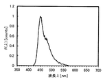
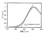
- FIGS. 1A and 1B are diagrams illustrating a method for calculating an average value (E ave ) of photon energy of light emitted from a luminescent center substance in a solution state.
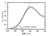
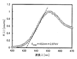
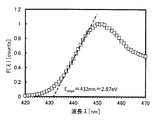
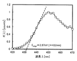
- FIG. 2 is a diagram for explaining a method of calculating the emission edge energy (E edge ) on the short wavelength side of the emission spectrum.
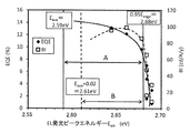
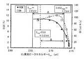
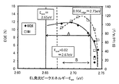
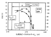
- FIG. 3 is a diagram for explaining the relationship between the EL emission peak energy (E em ) of the light-emitting element, the external quantum efficiency (EQE), and the blue index (BI).
- 4A and 4B are conceptual diagrams of light-emitting elements.
- 5A and 5B are conceptual diagrams of an active matrix light-emitting device.
- 6A and 6B are diagrams illustrating a lighting device.
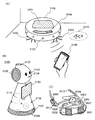
- FIG. 7A, 7B1, 7B2, and 7C are diagrams illustrating electronic devices.
- 8A to 8C are diagrams illustrating a light source device.
- FIG. 9 is a diagram illustrating a lighting device.
- FIG. 10 shows a lighting device.
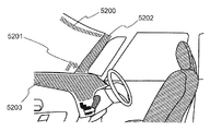
- FIG. 11 is a diagram illustrating an in-vehicle display device and a lighting device.
- 12A and 12B illustrate electronic devices.
- 13A to 13C each illustrate an electronic device.
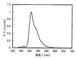
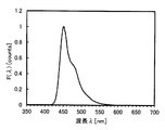
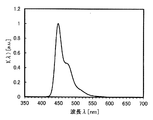
- FIG. 14 shows toluene of N, N′-diphenyl-N, N′-bis [3- (9-phenyl-9H-fluoren-9-yl) phenyl] pyrene-1,6-diamine (abbreviation: 1,6mFLPAPrn). It is the emission spectrum in a solution.
- FIG. 14 shows toluene of N, N′-diphenyl-N, N′-bis [3- (9-phenyl-9H-fluoren-9-yl) phen
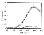
- FIG. 15 is a diagram for explaining a method of calculating the light emission edge on the short wavelength side of the PL spectrum in a toluene solution of 1,6 mM emFLPAPrn.
- FIG. 16 is a graph showing a relationship between external quantum efficiency (EQE) and blue index (BI) with respect to light emission peak energy (E em ) in the light-emitting elements 1-1 to 1-8.
- EQE external quantum efficiency
- BI blue index
- E em light emission peak energy
- FIG. 17 shows N, N′-bis (3-methylphenyl) -N, N′-bis [3- (9-phenyl-9H-fluoren-9-yl) phenyl] -pyrene-1,6-diamine (abbreviation) : 1,6mMemFLPAPrn) in a toluene solution.
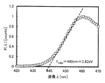
- FIG. 18 is a diagram for explaining a method of calculating the light emission end on the short wavelength side of the PL spectrum in a toluene solution of 1,6 mM emFLPAPrn.
- FIG. 19 is a graph showing a relationship between external quantum efficiency (EQE) and blue index (BI) with respect to light emission peak energy (E em ) in the light-emitting elements 2-1 to 2-8.
- FIG. 20 shows N, N ′-(pyrene-1,6-diyl) bis [(6, N-diphenylbenzo [b] naphtho [1,2-d] furan) -8-amine] (abbreviation: 1,6BnfAPrn).
- -03) is a diagram showing an emission spectrum in a toluene solution.
- FIG. 21 is a diagram for explaining a method of calculating the light emission edge on the short wavelength side of the PL spectrum in a toluene solution of 1,6BnfAPrn-03.
- FIG. 22 is a graph showing a relationship between external quantum efficiency (EQE) and blue index (BI) with respect to light emission peak energy (E em ) in the light-emitting elements 3-1 to 3-8.
- 23 shows N, N ′-(pyrene-1,6-diyl) bis [(6, N-diphenylbenzo [b] naphtho [1,2-d] furan) -8-amine] (abbreviation: 1,6BnfAPrn).
- -03) is a diagram showing an emission spectrum in a toluene solution.
- FIG. 24 is a diagram for explaining a method for calculating a light emitting end on the short wavelength side of a PL spectrum in a toluene solution of 1,6BnfAPrn-03.
- FIG. 25 is a graph showing a relationship between external quantum efficiency (EQE) and blue index (BI) with respect to light emission peak energy (E em ) in the light-emitting elements 4-1 to 4-4.
- EQE external quantum efficiency
- BI blue index
- E em light emission peak energy
- FIG. 26 shows N, N ′-(pyrene-1,6-diyl) bis (N-phenyl-6-cyclohexylbenzo [b] naphtho [1,2-d] furan-8-amine) (abbreviation: 1,6chBnfAPrn) It is a figure showing the emission spectrum in the toluene solution of).
- FIG. 27 is a diagram for explaining a method for calculating a light emitting edge on the short wavelength side of a PL spectrum in a toluene solution of 1,6chBnfAPrn.
- FIG. 28 is a graph showing a relationship between external quantum efficiency (EQE) and blue index (BI) with respect to light emission peak energy (E em ) in the light-emitting elements 5-1 to 5-8.
- FIG. 29 shows 3,10-bis [N- (9-phenyl-9H-carbazol-2-yl) -N-phenylamino] naphtho [2,3-b; 6,7-b ′] bisbenzofuran (abbreviation: It is a figure showing the emission spectrum in the toluene solution of 3,10PCA2Nbf (IV) -02).
- FIG. 29 shows 3,10-bis [N- (9-phenyl-9H-carbazol-2-yl) -N-phenylamino] naphtho [2,3-b; 6,7-b ′] bisbenzofuran (abbreviation: It is a figure showing the emission spectrum in the toluene solution of 3,10PCA2Nbf (IV) -02).
- FIG. 30 is a diagram for explaining a method for calculating the light emission edge on the short wavelength side of the PL spectrum in a toluene solution of 3,10PCA2Nbf (IV) -02.
- FIG. 31 is a graph showing a relationship between external quantum efficiency (EQE) and blue index (BI) with respect to light emission peak energy (E em ) in the light-emitting elements 6-1 to 6-8.
- EQE external quantum efficiency
- BI blue index
- E em light emission peak energy
- FIG. 32 shows 3,10-bis [N- (dibenzofuran-3-yl) -N-phenylamino] naphtho [2,3-b; 6,7-b ′] bisbenzofuran (abbreviation: 3,10FrA2Nbf (IV)) It is a figure showing the emission spectrum in the toluene solution of (-02).
- FIG. 33 is a diagram for explaining a method for calculating the light emission edge on the short wavelength side of the PL spectrum in a toluene solution of 3,10FrA2Nbf (IV) -02.
- FIG. 34 is a graph showing a relationship between external quantum efficiency (EQE) and blue index (BI) with respect to light emission peak energy (E em ) in the light-emitting elements 7-1 to 7-8.
- EQE external quantum efficiency
- BI blue index
- OLEDs so-called organic EL elements
- OLEDs are LEDs that use an organic compound as a light-emitting center substance, in contrast to LEDs in which an inorganic compound is a light-emitting center. It is known that an organic compound exhibits a broad emission spectrum as compared with an inorganic compound due to the influence of vibration levels and the like.
- the use of a microcavity structure capable of amplifying light of a target wavelength is advantageous in that it has less loss of light emission and is efficient.
- the light-emitting element having a microcavity structure with an appropriate optical path length and a color filter in combination the light-emitting element that can reduce light having a wavelength to be cut and emits light with high efficiency and high color purity. Can be obtained.
- the use of the microcavity structure is suitable for improving color purity and maintaining light emission efficiency.
- the organic EL element is a light emitting element using an organic compound as a light emission center substance as described above, and the spectrum of light emitted from the organic compound has a wavelength and a shape derived from the structure of the organic compound. It is unique to the substance. Therefore, the wavelength range in which light emission can be obtained efficiently differs depending on what kind of luminescent center material is used in the light emitting element.
- a light-emitting element satisfying the following formula (1) in a light-emitting element having a microcavity structure is a light-emitting element having good light-emitting efficiency (quantum efficiency calculated from front luminance).
- E ave is an average value of photon energy of light emitted from the luminescent center substance used in the light-emitting element in a solution state
- E em is photon energy of peak wavelength of light emitted from the light-emitting element
- E edge Is the emission edge energy on the short wavelength side of the emission spectrum of the emission center substance in the solution state
- the unit is all [eV].
- FIG. 1A shows a normalized emission spectrum in a toluene solution of an organic compound that exhibits blue light emission.
- the vertical axis is proportional to the photon count.
- the energy ⁇ p ( ⁇ ) of a photon having a certain wavelength can be expressed as the following formula (II).
- c represents the speed of light and h represents the Planck constant.
- the total energy in the entire wavelength region per unit time of light emission in the toluene solution of the organic compound can be represented by the following formula (III).
- the average photon energy (E ave ) of light emission is a value obtained by dividing the total energy represented by the above formula (III) by the total number of photons represented by the above formula (I). Can be represented.
- the average photon energy (E ave ) of light emission in the toluene solution of the organic compound whose emission spectrum is shown in FIG. 1 (A) can be calculated as 2.65 eV, that is, 468 nm from the above formula (IV) (FIG. 1 ( B)).
- the significant number is 3 digits.
- the vertical axis of the PL spectrum is not the photon number N p ( ⁇ ) but the energy ⁇ p ( ⁇ ) itself (for example, in the case of a spectral radiance meter), or the energy ⁇ p ( ⁇ ) May be a normalized spectrum I ( ⁇ ) that is proportional to.
- the average photon energy E ave of light emission can be obtained as follows.
- the average photon energy (E ave ) of light emission is obtained from the formulas (III) to (V) as in the following formula (VI) when the vertical axis of the PL spectrum is the energy ⁇ p ( ⁇ ) itself. Can do.
- the average photon energy (E ave ) of luminescence is calculated using any one of the above formulas (IV), (VI), or (VII) depending on the instrument that measures the emission spectrum of the organic compound in the toluene solution. Can be sought.
- FIG. 2 is an enlarged view of the vicinity of the light emission end on the short wavelength side of the emission center substance used in FIG. As shown in FIG. 2, E edge can be obtained from the intersection of the tangent line and the x axis by drawing a tangent line near the half value at the short wavelength side skirt of the emission spectrum F ( ⁇ ).
- the emission edge energy (E edge ) can be calculated to be 2.87 eV.
- the PL spectrum of the luminescent center substance used for calculating E ave and E edge is a spectrum in a solution state.
- Each energy level is affected by the relative dielectric constant of the medium. Since the relative dielectric constant of the organic compound constituting the EL layer of the light-emitting element is about 3, it is approximately accurate by measuring in a solvent having a relative dielectric constant of 1 to 10 at room temperature, more preferably 2 to 5 at room temperature. Can be measured. Specific examples of the solvent include hexane, benzene, toluene, diethyl ether, ethyl acetate, chloroform, chlorobenzene, and dichloromethane.
- toluene and chloroform have a relative dielectric constant of 2 to 5 at room temperature, are highly soluble, and are general-purpose solvents. Therefore, when measured in toluene or chloroform, the values in the light-emitting element and those solvents In many cases, the difference in values is within the experimental error range.
- FIG. 3 shows the relationship between E em and EQE and the relationship between E em and BI with respect to an organic EL element (top emission) having a microcavity structure with the light emitting material used in FIGS. It has been investigated.
- the EQE here is an uncorrected EQE calculated by assuming Lambertian light distribution from the front luminance. Further, EQE is used when the luminance is around 1000 cd / m 2 .
- the blue index (BI) is a value obtained by further dividing the current efficiency (cd / A) by the y chromaticity, and is one of indexes indicating the emission characteristics of blue light emission. Blue light emission tends to emit light with higher color purity as the y chromaticity is smaller. Blue light emission with high color purity can express a wide range of blue even if the luminance component is small, and the use of blue light emission with high color purity reduces the luminance required to express blue. Therefore, the power consumption can be reduced.
- BI considering y chromaticity, which is one of the indicators of blue purity, is preferably used as a means for expressing blue light emission efficiency, and a light emitting element having a higher BI has better efficiency as a blue light emitting element used in a display. It can be said that there is.
- the EL emission peak energy (E em ) shown on the horizontal axis of FIG. 3 can be adjusted by changing the optical path length of the organic EL element and changing the wavelength to be amplified by the microcavity effect.
- E em the efficiency of the light emitting device exhibiting good efficiency in the range between 2.65 eV and 2.73 eV (the range of A in the figure) and the E em higher than that is greatly reduced. I understand that. In the same range, BI also shows a good value. Note that, as calculated above, 2.65 eV corresponds to the average photon energy (E ave ) of light emission in the toluene solution of the luminescent center substance used in these light-emitting elements.
- the upper limit value of 2.73 eV in the range A in the figure is the emission edge energy (E) on the short wavelength side of the PL emission spectrum in the toluene solution of the emission center substance used in these organic EL elements calculated above. edge ) which corresponds to 0.95 times 2.87 eV.
- BI also shows a good numerical value.
- E ave represents the average photon energy (unit [eV]) of light emission in the toluene solution of the emission center substance used in the light emitting element, and E edge is the short wavelength of the PL emission spectrum in the toluene solution of the emission center substance.
- the side emission edge energy (unit [eV]) is represented, and E em represents the EL emission peak energy (unit [eV]).
- BI In the case of an organic EL element that emits blue light, it is appropriate to pay attention to BI.
- the present inventors have found that BI and EQE differ from each other in E em that reaches a peak. As shown in FIG. 3, since BI has a maximum value when E em is located in a relatively high energy region as compared to EQE, the microcavity structure has a relationship as shown in the following equation (2). It is preferable to control the cavity length (optical path length).
- E em is preferably 2.6 eV or more and 2.9 eV or less.
- the organic EL element of one embodiment of the present invention is a light-emitting element having a microcavity structure.
- An organic EL element emits light by passing an electric current with an EL layer containing an organic compound sandwiched between a pair of electrodes, but the microcavity structure has one of a pair of electrodes, a reflective electrode and the other half.
- a transmissive / semi-reflective electrode By using a transmissive / semi-reflective electrode, reflection is repeated and light having a wavelength corresponding to the distance between the electrodes (also referred to as a cavity length or an optical path length) can be amplified.
- the cavity length can be changed by adjusting the thickness of the EL layer or electrode.
- a transparent electrode such as ITO can be used.
- the optical path length can be controlled by adjusting the thickness of the carrier transport layer or the carrier injection layer.
- the light emission direction of the organic EL element may be a top emission structure or a bottom emission structure.
- an organic compound layer having a molecular weight of 300 or more and 1200 or less is formed on the surface of the transflective electrode opposite to the surface with respect to the reflective electrode in order to more effectively extract light. It is preferable that
- the emission center substance in one light-emitting element is preferably one kind.
- the light-emitting element of one embodiment of the present invention having the above structure can be a light-emitting element with favorable emission efficiency.
- the light-emitting element in this embodiment includes a pair of electrodes including a first electrode 101 and a second electrode 102, and an EL layer 103 provided between the first electrode 101 and the second electrode 102. It consists of and.
- the electrode provided on the manufacturing substrate side is described as the first electrode 101.
- the light-emitting element of one embodiment of the present invention is a light-emitting element having a microcavity structure.
- a light-emitting element having a microcavity structure is obtained by forming a pair of electrodes of a light-emitting element from a reflective electrode and a semi-transmissive / semi-reflective electrode.
- the reflective electrode and the semi-transmissive / semi-reflective electrode correspond to the first electrode 101 and the second electrode 102 described above.
- At least an EL layer is provided, and at least a light-emitting layer serving as a light-emitting region is provided.
- a light emitting element having a microcavity structure In a light emitting element having a microcavity structure, light emitted in all directions from a light emitting layer included in an EL layer is reflected by a reflective electrode and a semi-transmissive / semi-reflective electrode and resonates.
- the reflective electrode has a visible light reflectance of 40% to 100%, preferably 70% to 100%, and a resistivity of 1 ⁇ 10 ⁇ 2 ⁇ cm or less.
- the material for forming the reflective electrode include aluminum (Al) or an alloy containing Al.
- the alloy containing Al include an alloy containing Al and L (L represents one or more of titanium (Ti), neodymium (Nd), nickel (Ni), and lanthanum (La)).
- Aluminum has a low resistance value and a high light reflectance. In addition, since aluminum is abundant in the crust and inexpensive, manufacturing cost of a light-emitting element by using aluminum can be reduced.
- N is yttrium (Y), Nd, magnesium (Mg), ytterbium (Yb), Al, Ti, gallium (Ga), zinc (Zn), indium (In) Represents one or more of tungsten (W), manganese (Mn), tin (Sn), iron (Fe), Ni, copper (Cu), palladium (Pd), iridium (Ir), or gold (Au) ) And the like.
- the alloy containing silver include an alloy containing silver, palladium and copper, an alloy containing silver and copper, an alloy containing silver and magnesium, an alloy containing silver and nickel, an alloy containing silver and gold, and silver and ytterbium. Examples thereof include alloys.
- transition metals such as tungsten, chromium (Cr), molybdenum (Mo), copper, and titanium can be used.
- a transparent electrode layer can be formed using a light-transmitting conductive material between the reflective electrode and the EL layer, and the first electrode 101 can be formed using two layers of the reflective electrode and the transparent electrode.
- the optical path length (cavity length) of the cavity structure can also be adjusted.
- the light-transmitting conductive material examples include indium tin oxide (Indium Tin Oxide, hereinafter referred to as ITO), indium tin oxide containing silicon or silicon oxide (abbreviation: ITSO), indium zinc oxide (Indium Zinc Oxide), Examples thereof include metal oxides such as indium oxide-tin oxide containing titanium, indium-titanium oxide, tungsten oxide, and indium oxide containing zinc oxide.
- ITO Indium Tin Oxide
- ITSO indium tin oxide containing silicon or silicon oxide
- ITSO indium zinc oxide
- metal oxides such as indium oxide-tin oxide containing titanium, indium-titanium oxide, tungsten oxide, and indium oxide containing zinc oxide.
- the first electrode 101 is composed of the reflective electrode 101-1 and the transparent electrode 101-2.
- the transflective electrode has a visible light reflectance of 20% to 80%, preferably 40% to 70%, and a resistivity of 1 ⁇ 10 ⁇ 2 ⁇ cm or less.
- the semi-transmissive / semi-reflective electrode can be formed using one or more kinds of conductive metals, alloys, conductive compounds, and the like. Specifically, for example, indium tin oxide (hereinafter referred to as ITO), indium tin oxide containing silicon or silicon oxide (abbreviation: ITSO), indium zinc oxide (indium zinc oxide), and titanium are included.
- ITO indium tin oxide
- ITSO indium tin oxide containing silicon or silicon oxide
- ITSO indium zinc oxide
- titanium titanium
- Metal oxides such as indium oxide containing indium oxide-tin oxide, indium-titanium oxide, tungsten oxide, and zinc oxide can be used.
- a metal thin film with a thickness that allows light to pass therethrough (preferably, a thickness of 1 nm to 30 nm) can be used.
- the metal for example, Ag or an alloy such as Ag and Al, Ag and Mg, Ag and Au, Ag and Yb, or the like can be used.
- the reflective electrode and the semi-transmissive / semi-reflective electrode may be either the first electrode 101 or the second electrode 102.
- FIG. 4A illustrates the case where the first electrode 101 is on the manufacturing substrate side as described above. Therefore, when the reflective electrode is the first electrode, the light-emitting element has a top emission structure. When the reflective electrode is the second electrode 102, a bottom emission light-emitting element is obtained. Note that the first electrode 101 and the second electrode 102 may be an anode or a cathode, but FIG. 4A illustrates the case where the first electrode 101 is an anode.
- the light extraction efficiency can be improved by providing the organic cap layer 104 on a surface opposite to the surface in contact with the EL layer 103 of the second electrode 102.
- the organic cap layer 104 by providing the organic cap layer 104 so as to be in contact with the electrode 102, a difference in refractive index between the electrode 102 and the air interface can be reduced, so that light extraction efficiency can be improved.
- the film thickness is preferably 5 nm to 120 nm. More preferably, it is 30 nm or more and 90 nm or less.
- the organic cap layer 104 is preferably an organic compound layer having a molecular weight of 300 to 1200.
- the second electrode 102 is a semi-transmissive / semi-reflective electrode, and it is necessary to reduce the film thickness in order to maintain a certain degree of translucency, which may deteriorate conductivity.
- a conductive material for the organic cap layer 104 it is possible to secure the conductivity and improve the yield of manufacturing the light emitting element while improving the light extraction efficiency.
- an organic compound with little absorption in the visible light region can be preferably used.
- the organic compound used for the EL layer 103 can also be used as the organic cap layer 104. In this case, the organic cap layer 104 can be easily formed because the organic cap layer 104 can be formed in the film formation apparatus or the film formation chamber in which the EL layer 103 is formed.
- the light-emitting element is an optical element between the reflective electrode and the semi-transmissive / semi-reflective electrode by changing the thickness of the transparent electrode provided in contact with the reflective electrode and the thickness of the carrier transport layer such as the hole injection layer and the hole transport layer.
- the distance (cavity length) can be changed.
- FIG. 4A shows an example in which the optical path length is adjusted by the transparent electrode 101-2 which is a part of the first electrode 101, but the optical path is formed by the hole injection layer 111 as shown in FIG.
- the length may be adjusted, may be adjusted by the hole transport layer 112, or two or more of these may be used in combination.
- the light reflected by the reflective electrode has a large interference with the light (first incident light) directly incident on the semi-transmissive / semi-reflective electrode from the light emitting layer. Therefore, it is preferable to adjust the optical distance between the reflective electrode and the light emitting layer to (2n-1) ⁇ / 4 (where n is a natural number of 1 or more and ⁇ is the wavelength of light emission to be amplified). By adjusting the optical distance, the phase of the first reflected light and the first incident light can be matched to further amplify the light emission from the light emitting layer.
- the EL layer 103 preferably has a laminated structure, but the laminated structure is not particularly limited, and a hole injection layer, a hole transport layer, an electron transport layer, an electron injection layer, a carrier block layer, an exciton Various layer structures such as a block layer and a charge generation layer can be applied.
- the hole injection layer 111 is a layer containing a substance having an acceptor property.
- a substance having an acceptor property any of an organic compound and an inorganic compound can be used.
- a compound having an electron withdrawing group (halogen group or cyano group) can be used, and 7,7,8,8-tetracyano-2,3,5,6-tetrafluoroquinodimethane.
- F4-TCNQ 4,7,8,8-tetracyano-2,3,5,6-tetrafluoroquinodimethane
- HAT-CN 2,3,6,7,10,11-hexacyano-1,4 , 5,8,9,12-hexaazatriphenylene
- F6-TCNNQ 1,3,4,5,7,8-hexafluorotetracyano-naphthoquinodimethane
- a compound having an electron-withdrawing group can be used.
- the organic compound having acceptor properties a compound in which an electron withdrawing group is bonded to a condensed aromatic ring having a plurality of heteroatoms such as HAT-CN is preferable because it is thermally stable.
- Radialene derivatives having an electron-withdrawing group are preferable because of their very high electron-accepting properties.
- ⁇ , ⁇ ′, ⁇ ′′ 1,2,3-cyclopropanetriylidenetris [4-cyano-2,3,5,6-tetrafluorobenzeneacetonitrile], ⁇ , ⁇ ′, ⁇ ′′ -1,2,3-cyclopropanetriylidenetris [2,6-dichloro-3,5-difluoro-4- (trifluoromethyl) benzeneacetonitrile], ⁇ , ⁇ ′, ⁇ ′′ -1,2,3-cyclopropanetriylidentris [2,3,4, 5,6-pentafluorobenzeneacetonitrile] and the like.
- molybdenum oxide, vanadium oxide, ruthenium oxide, tungsten oxide, manganese oxide, or the like can be used as the acceptor substance.
- phthalocyanine-based complex compounds such as phthalocyanine (abbreviation: H 2 Pc) and copper phthalocyanine (CuPC), 4,4′-bis [N- (4-diphenylaminophenyl) -N-phenylamino] biphenyl (abbreviation) : DPAB), N, N′-bis ⁇ 4- [bis (3-methylphenyl) amino] phenyl ⁇ -N, N′-diphenyl- (1,1′-biphenyl) -4,4′-diamine (abbreviation) :
- the hole injection layer 111 is also formed by an aromatic amine compound such as DNTPD) or a polymer such as poly (3,4-ethylenedioxythiophene) / poly (styrenesulf
- a composite material in which an acceptor substance is contained in a substance having a hole-transport property can be used for the hole-injecting layer 111.
- a material for forming an electrode can be selected regardless of a work function. That is, not only a material with a high work function but also a material with a low work function can be used for the first electrode 101.
- acceptor substance 7,7,8,8-tetracyano-2,3,5,6-tetrafluoroquinodimethane (abbreviation: F4-TCNQ), chloranil, 1,3,4,5,7,
- F4-TCNQ 7,7,8,8-tetracyano-2,3,5,6-tetrafluoroquinodimethane
- chloranil 1,3,4,5,7
- An organic compound having an acceptor property such as 8-hexafluorotetracyano-naphthoquinodimethane (abbreviation: F6-TCNNQ) and a transition metal oxide
- F6-TCNNQ 8-hexafluorotetracyano-naphthoquinodimethane
- a transition metal oxide an oxide of a metal belonging to Groups 4 to 8 in the periodic table can be used.
- vanadium oxide, niobium oxide, tantalum oxide, chromium oxide, molybdenum oxide, tungsten oxide, manganese oxide, rhenium oxide, and the like have high electron-accepting properties. Therefore, it is preferable.
- molybdenum oxide is especially preferable because it is stable in the air, has a low hygroscopic property, and is easy to handle.
- the hole-transporting substance used for the composite material various organic compounds such as aromatic amine compounds, carbazole derivatives, aromatic hydrocarbons, and high molecular compounds (oligomers, dendrimers, polymers, and the like) can be used.
- the hole-transporting substance used for the composite material is preferably a substance having a hole mobility of 10 ⁇ 6 cm 2 / Vs or higher.
- organic compounds that can be used as the hole transporting substance in the composite material are specifically listed.
- N, N′-di (p-tolyl) -N, N′-diphenyl-p-phenylenediamine abbreviation: DTDPPA
- 4,4′-bis [ N- (4-diphenylaminophenyl) -N-phenylamino] biphenyl abbreviation: DPAB
- N, N′-bis ⁇ 4- [bis (3-methylphenyl) amino] phenyl ⁇ -N, N′-diphenyl -(1,1′-biphenyl) -4,4′-diamine abbreviation: DNTPD
- DPA3B 1,3-bis- (4-bis (4-methyl-phenyl) -amino-phenyl) -cyclohexane
- carbazole derivative examples include 3- [N- (9-phenylcarbazol-3-yl) -N-phenylamino] -9-phenylcarbazole (abbreviation: PCzPCA1), 3,6-bis [N— (9-phenylcarbazol-3-yl) -N-phenylamino] -9-phenylcarbazole (abbreviation: PCzPCA2), 3- [N- (1-naphthyl) -N- (9-phenylcarbazol-3-yl) Amino] -9-phenylcarbazole (abbreviation: PCzPCN1), 4,4′-di (N-carbazolyl) biphenyl (abbreviation: CBP), 1,3,5-tris [4- (N-carbazolyl) phenyl] benzene ( Abbreviation: TCPB), 9- [4- (10-phenylanthracen-9-yl) phenyl]
- aromatic hydrocarbon examples include 2-tert-butyl-9,10-di (2-naphthyl) anthracene (abbreviation: t-BuDNA), 2-tert-butyl-9,10-di (1-naphthyl).
- pentacene, coronene, and the like can also be used. It may have a vinyl skeleton.
- aromatic hydrocarbon having a vinyl group for example, 4,4′-bis (2,2-diphenylvinyl) biphenyl (abbreviation: DPVBi), 9,10-bis [4- (2,2- Diphenylvinyl) phenyl] anthracene (abbreviation: DPVPA) and the like.
- DPVBi 4,4′-bis (2,2-diphenylvinyl) biphenyl
- DPVPA 9,10-bis [4- (2,2- Diphenylvinyl) phenyl] anthracene
- poly (N-vinylcarbazole) (abbreviation: PVK), poly (4-vinyltriphenylamine) (abbreviation: PVTPA), poly [N- (4- ⁇ N ′-[4- (4-diphenylamino)] Phenyl] phenyl-N′-phenylamino ⁇ phenyl) methacrylamide] (abbreviation: PTPDMA), poly [N, N′-bis (4-butylphenyl) -N, N′-bis (phenyl) benzidine] (abbreviation: Polymer compounds such as Poly-TPD can also be used.
- the hole injecting layer 111 By forming the hole injecting layer 111, the hole injecting property is improved and a light emitting element with a low driving voltage can be obtained.
- An organic compound having an acceptor property is an easy-to-use material because it can be easily deposited and easily formed into a film.
- the composite material has good conductivity. Therefore, even if it is formed as a thick film, the drive voltage is hardly deteriorated, and the cavity length in the microcavity structure is adjusted. It is very suitable as a layer to perform.
- the hole transport layer 112 is formed including a material having a hole transport property.
- the material having a hole transporting property preferably has a hole mobility of 1 ⁇ 10 ⁇ 6 cm 2 / Vs or more.
- the hole-transport layer 112 preferably contains the organic compound of one embodiment of the present invention. By including the organic compound described in Embodiment 1 in the hole-transport layer 112, a layer having a low refractive index can be formed inside the EL layer 103, and the external quantum efficiency of the light-emitting element can be improved. Become.
- Examples of the material having a hole transporting property include 4,4′-bis [N- (1-naphthyl) -N-phenylamino] biphenyl (abbreviation: NPB), N, N′-bis (3-methylphenyl).
- the light emitting layer 113 is a layer containing a host material and a light emitting material.
- the light emitting material may be a fluorescent light emitting material, a phosphorescent light emitting material, a material exhibiting thermally activated delayed fluorescence (TADF), or another light emitting material. Moreover, even if it is a single layer, it may consist of a plurality of layers containing different light emitting materials.
- Examples of materials that can be used as the fluorescent light-emitting substance in the light-emitting layer 113 include the following. Other fluorescent materials can also be used.
- condensed aromatic diamine compounds typified by pyrenediamine compounds such as 1,6FLPAPrn, 1,6mMemFLPAPrn, and 1,6BnfAPrn-03 are preferable because they have high hole trapping properties and are excellent in luminous efficiency and reliability.
- Examples of materials that can be used as the phosphorescent material in the light-emitting layer 113 include the following.
- a rare earth metal complex such as tris (acetylacetonato) (monophenanthroline) terbium (III) (abbreviation: [Tb (acac) 3 (Phen)]) can be given. These are compounds that mainly emit green phosphorescence, and have an emission peak at 500 nm to 600 nm. Note that an organometallic iridium complex having a pyrimidine skeleton is particularly preferable because of its outstanding reliability and luminous efficiency.
- a known phosphorescent light emitting material may be selected and used.
- TADF material fullerene and its derivatives, acridine and its derivatives, eosin derivatives and the like can be used.
- metal-containing porphyrins including magnesium (Mg), zinc (Zn), cadmium (Cd), tin (Sn), platinum (Pt), indium (In), palladium (Pd), and the like can be given.
- the metal-containing porphyrin include a protoporphyrin-tin fluoride complex (SnF 2 (Proto IX)), a mesoporphyrin-tin fluoride complex (SnF 2 (Meso IX)) represented by the following structural formula, and hematoporphyrin.
- the heterocyclic compound has a ⁇ -electron rich heteroaromatic ring and a ⁇ -electron deficient heteroaromatic ring, both the electron transport property and the hole transport property are high, which is preferable.
- a substance in which a ⁇ -electron rich heteroaromatic ring and a ⁇ -electron deficient heteroaromatic ring are directly bonded increases both the donor property of the ⁇ -electron rich heteroaromatic ring and the acceptor property of the ⁇ -electron deficient heteroaromatic ring. Since the energy difference between the S 1 level and the T 1 level is small, it is particularly preferable because thermally activated delayed fluorescence can be obtained efficiently.
- an aromatic ring to which an electron withdrawing group such as a cyano group is bonded may be used.
- various carrier transport materials such as a material having an electron transport property and a material having a hole transport property can be used.
- the substances mentioned as the material having a hole transporting property contained in the hole transporting layer 112 can be preferably used.
- bis (10-hydroxybenzo [h] quinolinato) beryllium (II) (abbreviation: BeBq 2 ), bis (2-methyl-8-quinolinolato) (4-phenylphenolato) Aluminum (III) (abbreviation: BAlq), bis (8-quinolinolato) zinc (II) (abbreviation: Znq), bis [2- (2-benzoxazolyl) phenolato] zinc (II) (abbreviation: ZnPBO), Metal complexes such as bis [2- (2-benzothiazolyl) phenolato] zinc (II) (abbreviation: ZnBTZ), 2- (4-biphenylyl) -5- (4-tert-butylphenyl) -1,3,4 -Oxadiazole (abbreviation: PBD), 3- (4-biphenylyl) -4-phenyl-5- (4-tert-butylpheny
- a heterocyclic compound having a diazine skeleton and a heterocyclic compound having a pyridine skeleton are preferable because of their good reliability.
- a heterocyclic compound having a diazine (pyrimidine or pyrazine) skeleton has a high electron transporting property and contributes to a reduction in driving voltage.
- a material having an anthracene skeleton is preferable as the host material.
- a substance having an anthracene skeleton is used as a host material for a fluorescent light-emitting substance, a light-emitting layer with favorable emission efficiency and durability can be realized.
- Many materials having an anthracene skeleton have deep HOMO levels, and thus can be favorably applied to one embodiment of the present invention.
- a substance having an anthracene skeleton used as a host material a diphenylanthracene skeleton, particularly a substance having a 9,10-diphenylanthracene skeleton, is preferable because it is chemically stable.
- the host material has a carbazole skeleton because hole injection / transport properties are improved.
- the HOMO level is about 0.1 eV than carbazole. It is more preferable because it becomes shallower and holes can easily enter.
- the host material contains a dibenzocarbazole skeleton, the HOMO level is shallower than carbazole by about 0.1 eV, which facilitates the entry of holes, and also has excellent hole transportability and high heat resistance. It is.
- a substance having a 9,10-diphenylanthracene skeleton and a carbazole skeleton (or a benzocarbazole skeleton or a dibenzocarbazole skeleton) at the same time is more preferable as a host material.
- a benzofluorene skeleton or a dibenzofluorene skeleton may be used instead of the carbazole skeleton.
- Examples of such a substance include 9-phenyl-3- [4- (10-phenyl-9-anthryl) phenyl] -9H-carbazole (abbreviation: PCzPA), 3- [4- (1-naphthyl)- Phenyl] -9-phenyl-9H-carbazole (abbreviation: PCPN), 9- [4- (10-phenyl-9-anthracenyl) phenyl] -9H-carbazole (abbreviation: CzPA), 7- [4- (10- Phenyl-9-anthryl) phenyl] -7H-dibenzo [c, g] carbazole (abbreviation: cgDBCzPA), 6- [3- (9,10-diphenyl-2-anthryl) phenyl] -benzo [b] naphtho [1 , 2-d] furan (abbreviation: 2 mBnfPPA), 9-phenyl-10-
- the host material may be a material in which a plurality of types of substances are mixed.
- a mixed host material it is preferable to mix a material having an electron transporting property and a material having a hole transporting property. .
- the exciplex selects a combination that forms an exciplex that emits light that overlaps with the wavelength of the absorption band on the lowest energy side of the light-emitting material, energy transfer becomes smooth and light can be emitted efficiently. preferable. Further, it is preferable to use the structure because the driving voltage is also reduced.
- One embodiment of the present invention is particularly suitable for a light-emitting element that emits blue light.
- the electron transport layer 114 is a layer containing a substance having an electron transport property.
- the substance having an electron transporting property those exemplified as the substance having an electron transporting property that can be used for the host material can be used.
- an alkali metal or an alkali such as lithium fluoride (LiF), cesium fluoride (CsF), calcium fluoride (CaF 2 ), or the like is used as the electron injection layer 115.
- a layer containing an earth metal or a compound thereof may be provided.
- the electron injecting layer 115 a layer made of a substance having an electron transporting property, an alkali metal, an alkaline earth metal, or a compound thereof, or electride may be used. Examples of the electride include a substance obtained by adding a high concentration of electrons to a mixed oxide of calcium and aluminum.
- a substance having an electron-transport property includes the above alkali metal or alkaline earth metal fluoride in a concentration or higher (50 wt% or more) in a microcrystalline state. It is also possible to use a stripped layer. Since the layer is a layer having a low refractive index, a light-emitting element with better external quantum efficiency can be provided.
- a charge generation layer 116 may be provided instead of the electron injection layer 115 (FIG. 4B).
- the charge generation layer 116 is a layer that can inject holes into a layer in contact with the cathode side of the layer and inject electrons into a layer in contact with the anode side by applying a potential.
- the charge generation layer 116 includes at least a P-type layer 117.
- the P-type layer 117 is preferably formed using the composite material mentioned as the material that can form the hole injection layer 111 described above. Further, the P-type layer 117 may be formed by stacking the above-described film containing an acceptor material and a film containing a hole transport material as a material constituting the composite material.
- the organic compound of one embodiment of the present invention is an organic compound having a low refractive index, a light-emitting element with favorable external quantum efficiency can be obtained by using it for the P-type layer 117.
- the charge generation layer 116 is preferably provided with one or both of an electron relay layer 118 and an electron injection buffer layer 119 in addition to the P-type layer 117.
- the electron relay layer 118 includes at least a substance having an electron transporting property, and has a function of smoothly transferring electrons by preventing the interaction between the electron injection buffer layer 119 and the P-type layer 117.
- the LUMO level of the substance having an electron transporting property contained in the electron relay layer 118 is the LUMO level of the acceptor substance in the P-type layer 117 and the substance contained in the layer in contact with the charge generation layer 116 in the electron transporting layer 114. It is preferably between the LUMO levels.
- the specific energy level of the LUMO level in the substance having an electron transporting property used for the electron relay layer 118 is ⁇ 5.0 eV or more, preferably ⁇ 5.0 eV or more and ⁇ 3.0 eV or less. Note that as the substance having an electron transporting property used for the electron relay layer 118, a phthalocyanine-based material or a metal complex having a metal-oxygen bond and an aromatic ligand is preferably used.
- the electron injection buffer layer 119 includes an alkali metal, an alkaline earth metal, a rare earth metal, and a compound thereof (including an alkali metal compound (including an oxide such as lithium oxide, a halide, and a carbonate such as lithium carbonate and cesium carbonate).
- Alkaline earth metal compounds (including oxides, halides, carbonates) or rare earth metal compounds (including oxides, halides, carbonates) can be used. It is.
- the electron injection buffer layer 119 is formed to include an electron transporting substance and a donor substance, an alkali metal, an alkaline earth metal, a rare earth metal, or a compound thereof (as a donor substance)
- Alkali metal compounds including oxides such as lithium oxide, halides, carbonates such as lithium carbonate and cesium carbonate
- alkaline earth metal compounds including oxides, halides, carbonates
- rare earth metal compounds In addition to (including oxides, halides, and carbonates), organic compounds such as tetrathianaphthacene (abbreviation: TTN), nickelocene, and decamethyl nickelocene can also be used.
- TTN tetrathianaphthacene
- nickelocene nickelocene
- decamethyl nickelocene can also be used.
- the substance having an electron transporting property can be formed using a material similar to the material of the electron transport layer 114 described above.
- a metal, an alloy, an electrically conductive compound, a mixture thereof, or the like having a low work function (specifically, 3.8 eV or less) can be used as a material for forming the second electrode 102.
- cathode materials include alkali metals such as lithium (Li) and cesium (Cs), and group 1 of the periodic table of elements such as magnesium (Mg), calcium (Ca), and strontium (Sr) Examples include elements belonging to Group 2, and alloys containing these (MgAg, AlLi), europium (Eu), ytterbium (Yb), and other rare earth metals, and alloys containing these.
- indium oxide-tin oxide containing Al, Ag, ITO, silicon or silicon oxide regardless of the work function.
- Various conductive materials such as the above can be used for the second electrode 102. These conductive materials can be formed by a dry method such as a vacuum evaporation method or a sputtering method, an inkjet method, a spin coating method, or the like. Alternatively, a sol-gel method may be used for a wet method, or a metal material paste may be used for a wet method.
- a formation method of the EL layer 103 various methods can be used regardless of a dry method or a wet method.
- a vacuum deposition method a gravure printing method, an offset printing method, a screen printing method, an ink jet method, a spin coating method, or the like may be used.
- each electrode or each layer described above may be formed by using different film forming methods.
- the structure of the layers provided between the first electrode 101 and the second electrode 102 is not limited to the above. However, in order to suppress quenching caused by the proximity of the light emitting region and the metal used for the electrode and the carrier injection layer, holes and electrons are separated from the first electrode 101 and the second electrode 102. A structure in which a light emitting region in which recombinations are provided is preferable.
- Embodiment 2 In this embodiment, a light-emitting device using the light-emitting element described in Embodiment 1 will be described.
- FIGS. 5A is a top view illustrating the light-emitting device
- FIG. 5B is a cross-sectional view taken along lines AB and CD of FIG. 5A.
- This light-emitting device includes a drive circuit portion (source line drive circuit) 601, a pixel portion 602, and a drive circuit portion (gate line drive circuit) 603 indicated by dotted lines, which control light emission of the light-emitting elements.
- Reference numeral 604 denotes a sealing substrate
- reference numeral 605 denotes a sealing material
- the inside surrounded by the sealing material 605 is a space 607.
- the lead wiring 608 is a wiring for transmitting a signal input to the source line driver circuit 601 and the gate line driver circuit 603, and a video signal, a clock signal, an FPC (flexible printed circuit) 609 serving as an external input terminal, Receives start signal, reset signal, etc.
- FPC flexible printed circuit
- a printed wiring board PWB
- the light-emitting device in this specification includes not only a light-emitting device body but also a state in which an FPC or a PWB is attached thereto.
- a driver circuit portion and a pixel portion are formed over the element substrate 610.
- a source line driver circuit 601 that is a driver circuit portion and one pixel in the pixel portion 602 are illustrated.
- the element substrate 610 is manufactured using a substrate made of glass, quartz, organic resin, metal, alloy, semiconductor, or the like, or a plastic substrate made of FRP (Fiber Reinforced Plastics), PVF (polyvinyl fluoride), polyester, acrylic resin, or the like. do it.
- FRP Fiber Reinforced Plastics
- PVF polyvinyl fluoride
- the structure of the transistor used for the pixel or the driver circuit there is no particular limitation on the structure of the transistor used for the pixel or the driver circuit.
- an inverted staggered transistor or a staggered transistor may be used.
- a top-gate transistor or a bottom-gate transistor may be used.
- the semiconductor material used for the transistor is not particularly limited, and for example, silicon, germanium, silicon carbide, gallium nitride, or the like can be used.
- an oxide semiconductor containing at least one of indium, gallium, and zinc, such as an In—Ga—Zn-based metal oxide, may be used.
- crystallinity of a semiconductor material used for the transistor there is no particular limitation on the crystallinity of a semiconductor material used for the transistor, and any of an amorphous semiconductor and a semiconductor having crystallinity (a microcrystalline semiconductor, a polycrystalline semiconductor, a single crystal semiconductor, or a semiconductor partially including a crystal region) is used. May be used. It is preferable to use a crystalline semiconductor because deterioration of transistor characteristics can be suppressed.
- an oxide semiconductor is preferably used for a semiconductor device such as a transistor used in a touch sensor described below.
- an oxide semiconductor having a wider band gap than silicon is preferably used.
- the oxide semiconductor preferably contains at least indium (In) or zinc (Zn).
- the oxide semiconductor includes an oxide represented by an In-M-Zn-based oxide (M is a metal such as Al, Ti, Ga, Ge, Y, Zr, Sn, La, Ce, or Hf). Is more preferable.
- the semiconductor layer has a plurality of crystal parts, and the crystal part has a c-axis oriented perpendicular to the formation surface of the semiconductor layer or the top surface of the semiconductor layer, and a grain boundary between adjacent crystal parts. It is preferable to use an oxide semiconductor film which does not contain any oxide.
- the transistor having the above semiconductor layer can hold charge accumulated in the capacitor through the transistor for a long time due to the low off-state current.
- the driving circuit can be stopped while maintaining the gradation of an image displayed in each display region. As a result, an electronic device with extremely low power consumption can be realized.
- a base film In order to stabilize the characteristics of the transistor, it is preferable to provide a base film.
- an inorganic insulating film such as a silicon oxide film, a silicon nitride film, a silicon oxynitride film, or a silicon nitride oxide film can be used, which can be formed as a single layer or a stacked layer.
- the base film is formed by sputtering, CVD (Chemical Vapor Deposition) (plasma CVD, thermal CVD, MOCVD (Metal Organic CVD), etc.), ALD (Atomic Layer Deposition), coating, printing, etc. it can. Note that the base film is not necessarily provided if not necessary.
- the FET 623 indicates one of the transistors formed in the drive circuit portion 601.
- the driving circuit may be formed of various CMOS circuits, PMOS circuits, or NMOS circuits.
- CMOS circuits complementary metal-oxide-semiconductor
- PMOS circuits PMOS circuits
- NMOS circuits NMOS circuits.
- a driver integrated type in which a driver circuit is formed over a substrate is shown; however, this is not necessarily required, and the driver circuit can be formed outside the substrate.
- the pixel portion 602 is formed by a plurality of pixels including the switching FET 611, the current control FET 612, and the first electrode 613 electrically connected to the drain thereof, but is not limited thereto.
- the pixel portion may be a combination of two or more FETs and a capacitor.
- an insulator 614 is formed so as to cover an end portion of the first electrode 613.
- a positive photosensitive acrylic resin film can be used.
- a curved surface having a curvature is formed at the upper end portion or the lower end portion of the insulator 614 in order to improve the coverage of an EL layer or the like to be formed later.
- a positive photosensitive acrylic resin is used as the material of the insulator 614
- a negative photosensitive resin or a positive photosensitive resin can be used as the insulator 614.
- An EL layer 616 and a second electrode 617 are formed over the first electrode 613.
- a material used for the first electrode 613 functioning as an anode a material having a high work function is preferably used.
- a stack of a titanium nitride film and a film containing aluminum as a main component, a three-layer structure including a titanium nitride film, a film containing aluminum as a main component, and a titanium nitride film can be used. Note that with a stacked structure, resistance as a wiring is low, good ohmic contact can be obtained, and a function as an anode can be obtained.
- the EL layer 616 is formed by various methods such as an evaporation method using an evaporation mask, an inkjet method, and a spin coating method.
- the EL layer 616 includes the structure described in Embodiment 1. Further, as another material forming the EL layer 616, a low molecular compound or a high molecular compound (including an oligomer and a dendrimer) may be used.
- the second electrode 617 formed over the EL layer 616 and functioning as a cathode a material having a low work function (Al, Mg, Li, Ca, or an alloy or compound thereof (MgAg, MgIn, AlLi etc.) is preferred.
- the second electrode 617 includes a thin metal film and a transparent conductive film (ITO, 2 to 20 wt% oxidation).
- ITO transparent conductive film
- a stack of indium oxide containing zinc, indium tin oxide containing silicon, zinc oxide (ZnO), or the like is preferably used.
- a light-emitting element is formed using the first electrode 613, the EL layer 616, and the second electrode 617.
- the light-emitting element is the light-emitting element described in Embodiment 1.
- the pixel portion includes a plurality of light-emitting elements, in the light-emitting device in this embodiment, both the light-emitting element described in Embodiment 1 and a light-emitting element having any other structure are mixed. You may do it.
- the sealing substrate 604 is bonded to the element substrate 610 with the sealant 605, whereby the light-emitting element 618 is provided in the space 607 surrounded by the element substrate 610, the sealing substrate 604, and the sealant 605. Yes.
- the space 607 is filled with a filler and may be filled with a sealing material in addition to the case of being filled with an inert gas (such as nitrogen or argon).
- an epoxy resin or glass frit is preferably used for the sealant 605. Moreover, it is desirable that these materials are materials that do not transmit moisture and oxygen as much as possible.
- a plastic substrate made of FRP (Fiber Reinforced Plastics), PVF (polyvinyl fluoride), polyester, acrylic resin, or the like can be used as a material for the sealing substrate 604.
- a protective film may be provided on the second electrode.
- the protective film may be formed of an organic resin film or an inorganic insulating film. Further, a protective film may be formed so as to cover the exposed portion of the sealant 605. The protective film can be provided so as to cover the exposed side surfaces of the surface and side surfaces of the pair of substrates, the sealing layer, the insulating layer, and the like.
- the protective film a material that hardly permeates impurities such as water can be used. Therefore, it is possible to effectively suppress the diffusion of impurities such as water from the outside to the inside.
- oxide, nitride, fluoride, sulfide, ternary compound, metal or polymer can be used as a material constituting the protective film.
- oxide, nitride, fluoride, sulfide, ternary compound, metal or polymer can be used.
- the protective film is preferably formed by using a film formation method having good step coverage (step coverage).
- a film formation method having good step coverage there is an atomic layer deposition (ALD: Atomic Layer Deposition) method.
- a material that can be formed by an ALD method is preferably used for the protective film.
- ALD method a dense protective film with reduced defects such as cracks and pinholes or a uniform thickness can be formed.
- damage to the processed member when forming the protective film can be reduced.
- a protective film that is uniform and has few defects can be formed on the surface having a complicated uneven shape, and the top surface, side surface, and back surface of the touch panel.
- the light-emitting device described in Embodiment 1 is used for the light-emitting device in this embodiment, a light-emitting device having favorable characteristics can be obtained. Specifically, since the light-emitting element described in Embodiment 1 has favorable light emission efficiency, a light-emitting device with low power consumption can be obtained.
- FIGS. 6B is a top view of the lighting device
- FIG. 6A is a cross-sectional view taken along line ef in FIG. 6B.
- a first electrode 401 is formed over a light-transmitting substrate 400 which is a support.
- the first electrode 401 corresponds to the first electrode 101 in Embodiment 1.
- the first electrode 401 is formed using a light-transmitting material.
- a pad 412 for supplying a voltage to the second electrode 404 is formed on the substrate 400.
- An EL layer 403 is formed over the first electrode 401.
- the EL layer 403 corresponds to the structure of the EL layer 103 in Embodiment 1. For these configurations, refer to the description.
- a second electrode 404 is formed so as to cover the EL layer 403.
- the second electrode 404 corresponds to the second electrode 102 in Embodiment 1.
- the second electrode 404 is formed using a highly reflective material.
- a voltage is supplied to the second electrode 404 by being connected to the pad 412.
- the lighting device described in this embodiment includes a light-emitting element including the first electrode 401, the EL layer 403, and the second electrode 404. Since the light-emitting element is a light-emitting element with high emission efficiency, the lighting device in this embodiment can be a lighting device with low power consumption.
- the substrate 400 on which the light-emitting element having the above structure is formed and the sealing substrate 407 are fixed using sealing materials 405 and 406 and sealed, whereby the lighting device is completed. Either one of the sealing materials 405 and 406 may be used.
- a desiccant can be mixed in the inner sealing material 406 (not shown in FIG. 6B), so that moisture can be adsorbed and reliability can be improved.
- an external input terminal can be obtained.
- an IC chip 420 mounted with a converter or the like may be provided thereon.
- the lighting device described in this embodiment uses the light-emitting element described in Embodiment 1 as an EL element, and can be a light-emitting device with low power consumption.
- Embodiment 4 examples of electronic devices each including the light-emitting element described in Embodiment 1 will be described.
- the light-emitting element described in Embodiment 1 has high emission efficiency and low power consumption.
- the electronic device described in this embodiment can be an electronic device including a light-emitting portion with low power consumption.
- a television device also referred to as a television or a television receiver
- a monitor for a computer a digital camera, a digital video camera, a digital photo frame
- a mobile phone a mobile phone
- Large-sized game machines such as portable telephones, portable game machines, portable information terminals, sound reproduction apparatuses, and pachinko machines. Specific examples of these electronic devices are shown below.
- FIG. 7A illustrates an example of a television device.
- a display portion 7103 is incorporated in a housing 7101.
- a structure in which the housing 7101 is supported by a stand 7105 is shown.
- Images can be displayed on the display portion 7103, and the display portion 7103 is formed by arranging the light-emitting elements described in Embodiment 1 in a matrix.
- the television device can be operated with an operation switch included in the housing 7101 or a separate remote controller 7110.
- Channels and volume can be operated with an operation key 7109 provided in the remote controller 7110, and an image displayed on the display portion 7103 can be operated.
- the remote controller 7110 may be provided with a display portion 7107 for displaying information output from the remote controller 7110.
- the television device is provided with a receiver, a modem, and the like.
- General TV broadcasts can be received by a receiver, and connected to a wired or wireless communication network via a modem, so that it can be unidirectional (sender to receiver) or bidirectional (sender and receiver). It is also possible to perform information communication between each other or between recipients).
- FIG. 7B1 illustrates a computer, which includes a main body 7201, a housing 7202, a display portion 7203, a keyboard 7204, an external connection port 7205, a pointing device 7206, and the like. Note that this computer is manufactured by using the light-emitting elements described in Embodiment 1 for the display portion 7203 in a matrix.
- the computer shown in FIG. 7B1 may have a form as shown in FIG.
- a computer in FIG. 7B2 includes a second display portion 7210 instead of the keyboard 7204 and the pointing device 7206.
- the second display portion 7210 is a touch panel type, and input can be performed by operating a display for input displayed on the second display portion 7210 with a finger or a dedicated pen.
- the second display portion 7210 can display not only an input display but also other images.
- the display portion 7203 may also be a touch panel.
- FIG. 7C illustrates an example of a mobile terminal.
- the mobile phone includes a display portion 7402 incorporated in a housing 7401, operation buttons 7403, an external connection port 7404, a speaker 7405, a microphone 7406, and the like.
- the cellular phone 7400 includes a display portion 7402 manufactured by arranging the light-emitting elements described in Embodiment 1 in a matrix.
- the portable terminal illustrated in FIG. 7C can have a structure in which information can be input by touching the display portion 7402 with a finger or the like. In this case, operations such as making a call or creating a mail can be performed by touching the display portion 7402 with a finger or the like.
- the first mode is a display mode mainly for displaying an image.
- the first is a display mode mainly for displaying images, and the second is an input mode mainly for inputting information such as characters.
- the third is a display + input mode in which the display mode and the input mode are mixed.
- the display portion 7402 may be set to a character input mode mainly for inputting characters, and an operation for inputting characters displayed on the screen may be performed. In this case, it is preferable to display a keyboard or number buttons on most of the screen of the display portion 7402.
- the orientation (portrait or horizontal) of the mobile terminal is determined, and the screen display of the display portion 7402 is automatically displayed. Can be switched automatically.
- the screen mode is switched by touching the display portion 7402 or operating the operation button 7403 of the housing 7401. Further, switching can be performed depending on the type of image displayed on the display portion 7402. For example, if the image signal to be displayed on the display unit is moving image data, the mode is switched to the display mode, and if it is text data, the mode is switched to the input mode.
- the screen mode is switched from the input mode to the display mode. You may control.
- the display portion 7402 can function as an image sensor. For example, personal authentication can be performed by touching the display portion 7402 with a palm or a finger and capturing an image of a palm print, a fingerprint, or the like. In addition, if a backlight that emits near-infrared light or a sensing light source that emits near-infrared light is used for the display portion, finger veins, palm veins, and the like can be imaged.
- the applicable range of the light-emitting device including the light-emitting element described in Embodiment 1 is so wide that the light-emitting device can be applied to electronic devices in various fields.
- an electronic device with low power consumption can be obtained.
- FIG. 8A is a schematic diagram illustrating an example of a cleaning robot.
- the cleaning robot 5100 includes a display 5101 disposed on the upper surface, a plurality of cameras 5102 disposed on the side surface, brushes 5103, and operation buttons 5104. Although not shown, the lower surface of the cleaning robot 5100 is provided with a tire, a suction port, and the like. In addition, the cleaning robot 5100 includes various sensors such as an infrared sensor, an ultrasonic sensor, an acceleration sensor, a piezo sensor, an optical sensor, and a gyro sensor. Moreover, the cleaning robot 5100 includes a wireless communication unit.
- the cleaning robot 5100 is self-propelled, can detect the dust 5120, and can suck the dust from the suction port provided on the lower surface.
- the cleaning robot 5100 can analyze an image captured by the camera 5102 and determine whether there is an obstacle such as a wall, furniture, or a step. In addition, when an object that is likely to be entangled with the brush 5103 such as wiring is detected by image analysis, the rotation of the brush 5103 can be stopped.
- the display 5101 can display the remaining battery level, the amount of dust sucked, and the like.
- the route on which the cleaning robot 5100 has traveled may be displayed on the display 5101.
- the display 5101 may be a touch panel, and the operation buttons 5104 may be provided on the display 5101.
- the cleaning robot 5100 can communicate with a portable electronic device 5140 such as a smartphone.
- An image captured by the camera 5102 can be displayed on the portable electronic device 5140. Therefore, the owner of the cleaning robot 5100 can know the state of the room even when away from home.
- the display on the display 5101 can be confirmed with a portable electronic device 5140 such as a smartphone.
- the light-emitting device of one embodiment of the present invention can be used for the display 5101.
- a robot 2100 illustrated in FIG. 8B includes an arithmetic device 2110, an illuminance sensor 2101, a microphone 2102, an upper camera 2103, a speaker 2104, a display 2105, a lower camera 2106, an obstacle sensor 2107, and a moving mechanism 2108.
- the microphone 2102 has a function of detecting a user's speaking voice, environmental sound, and the like.
- the speaker 2104 has a function of emitting sound.
- the robot 2100 can communicate with the user using the microphone 2102 and the speaker 2104.
- the display 2105 has a function of displaying various information.
- the robot 2100 can display information desired by the user on the display 2105.
- the display 2105 may be equipped with a touch panel. Further, the display 2105 may be an information terminal that can be removed, and is installed at a fixed position of the robot 2100 to enable charging and data transfer.
- the upper camera 2103 and the lower camera 2106 have a function of imaging the surroundings of the robot 2100.
- the obstacle sensor 2107 can detect the presence or absence of an obstacle in the traveling direction when the robot 2100 moves forward using the moving mechanism 2108.
- the robot 2100 can recognize the surrounding environment using the upper camera 2103, the lower camera 2106, and the obstacle sensor 2107, and can move safely.
- the light-emitting device of one embodiment of the present invention can be used for the display 2105.
- FIG. 8C illustrates an example of a goggle type display.
- the goggle type display includes, for example, a housing 5000, a display unit 5001, a speaker 5003, an LED lamp 5004, operation keys 5005 (including a power switch or an operation switch), a connection terminal 5006, and a sensor 5007 (force, displacement, position, speed). , Acceleration, angular velocity, number of revolutions, distance, light, liquid, magnetism, temperature, chemical, sound, time, hardness, electric field, current, voltage, power, radiation, flow rate, humidity, gradient, vibration, smell, or infrared
- the light-emitting device of one embodiment of the present invention can be used for the display portion 5001 and the second display portion 5002.
- FIG. 9 illustrates an example in which the light-emitting element described in Embodiment 1 is used for a table lamp which is a lighting device.
- the desk lamp illustrated in FIG. 9 includes a housing 2001 and a light source 2002.
- the light source 2002 the lighting device described in Embodiment 2 may be used.
- FIG. 10 illustrates an example in which the light-emitting element described in Embodiment 1 is used as an indoor lighting device 3001. Since the light-emitting element described in Embodiment 1 is a light-emitting element with high light emission efficiency, the lighting device can have low power consumption. Further, since the light-emitting element described in Embodiment 1 can have a large area, the light-emitting element can be used as a large-area lighting device. Further, since the light-emitting element described in Embodiment 1 is thin, it can be used as a thin lighting device.
- the light-emitting element described in Embodiment 1 can be mounted on a windshield or a dashboard of an automobile.
- FIG. 11 illustrates one mode in which the light-emitting element described in Embodiment 1 is used for a windshield or a dashboard of an automobile.
- Display regions 5200 to 5203 are display regions provided using the light-emitting element described in Embodiment 1.
- a display region 5200 and a display region 5201 are display devices on which the light-emitting elements described in Embodiment 1 provided on a windshield of an automobile are mounted.
- the light-emitting element described in Embodiment 1 can be a display device in a so-called see-through state in which a first electrode and a second electrode are formed using a light-transmitting electrode so that opposite sides can be seen through. . If it is a see-through display, it can be installed without obstructing the field of view even if it is installed on the windshield of an automobile. Note that in the case where a transistor for driving or the like is provided, a light-transmitting transistor such as an organic transistor using an organic semiconductor material or a transistor using an oxide semiconductor is preferably used.
- a display region 5202 is a display device on which the light-emitting element described in Embodiment 1 is provided in a pillar portion.
- the field of view blocked by the pillar can be complemented by projecting an image from the imaging means provided on the vehicle body.
- the display area 5203 provided in the dashboard portion compensates for the blind spot by projecting the image from the imaging means provided outside the vehicle from the field of view blocked by the vehicle body, and improves safety. Can do. By displaying the video so as to complement the invisible part, it is possible to check the safety more naturally and without a sense of incongruity.
- the display area 5203 can also provide various other information by displaying navigation information, speedometer and tachometer, mileage, fuel gauge, gear state, air conditioner settings, and the like.
- the display items and layout can be appropriately changed according to the user's preference. Note that these pieces of information can also be provided in the display areas 5200 to 5202.
- the display areas 5200 to 5203 can also be used as lighting devices.
- FIG. 12A and 12B show a foldable portable information terminal 5150.
- FIG. A foldable portable information terminal 5150 includes a housing 5151, a display region 5152, and a bent portion 5153.
- FIG. 12A shows the portable information terminal 5150 in a developed state.
- FIG. 12B illustrates the portable information terminal 5150 in a folded state. Although the portable information terminal 5150 has a large display area 5152, the portable information terminal 5150 is compact and excellent in portability when folded.
- the display region 5152 can be folded in half by a bent portion 5153.
- the bent portion 5153 includes an extendable member and a plurality of support members. When the bent portion 5153 is folded, the extendable member extends, and the bent portion 5153 has a radius of curvature of 2 mm or more, preferably 3 mm or more. It can be folded.
- the display area 5152 may be a touch panel (input / output device) equipped with a touch sensor (input device).
- the light-emitting device of one embodiment of the present invention can be used for the display region 5152.
- FIG. 13A to 13C show a foldable portable information terminal 9310.
- FIG. 13A illustrates the portable information terminal 9310 in a developed state.
- FIG. 13B illustrates the portable information terminal 9310 in a state in which the state is changing from one of the developed state or the folded state to the other.
- FIG. 13C illustrates the portable information terminal 9310 in a folded state.
- the portable information terminal 9310 is excellent in portability in the folded state and excellent in display listability due to a seamless wide display area in the expanded state.
- the display panel 9311 is supported by three housings 9315 connected by hinges 9313.
- the display panel 9311 may be a touch panel (input / output device) equipped with a touch sensor (input device).
- the display panel 9311 can be reversibly deformed from a developed state to a folded state by bending the two housings 9315 via the hinge 9313.
- the light-emitting device of one embodiment of the present invention can be used for the display panel 9311.
- a display region 9312 in the display panel 9311 is a display region located on a side surface of the portable information terminal 9310 in a folded state.
- an alloy film of silver (Ag), palladium (Pd), and copper (Cu) (Ag—Pd—Cu (APC) film) is formed as a reflective electrode on a glass substrate with a film thickness of 100 nm by a sputtering method.
- indium tin oxide containing silicon oxide (ITSO) was formed to a thickness of 85 nm as a transparent electrode by a sputtering method, whereby the first electrode 101 was formed.
- the electrode area was 4 mm 2 (2 mm ⁇ 2 mm).
- the surface of the substrate was washed with water, baked at 200 ° C. for 1 hour, and then subjected to UV ozone treatment for 370 seconds.
- the substrate is introduced into a vacuum vapor deposition apparatus whose internal pressure is reduced to about 10 ⁇ 4 Pa, vacuum baking is performed at 170 ° C. for 30 minutes in a heating chamber in the vacuum vapor deposition apparatus, and then the substrate is released for about 30 minutes. Chilled.
- the substrate on which the first electrode 101 is formed is fixed to a substrate holder provided in the vacuum evaporation apparatus so that the surface on which the first electrode 101 is formed is downward, and the first electrode 101 Further, 3- [4- (9-phenanthryl) -phenyl] -9-phenyl-9H-carbazole (abbreviation: PCPPn) and molybdenum oxide (VI) represented by the above structural formula (i) are formed by an evaporation method.
- the change of the optical path length of the light emitting element was realized by changing the film thickness of the hole injection layer 111.
- the thickness of the hole injection layer 111 is 10 nm
- the light emitting element 1-2 is 15 nm
- the light emitting element 1-3 is 20 nm
- the light emitting element 1-4 is 25 nm
- the light emitting element 1-5 is 30 nm
- the light emitting element 1-6 was manufactured to have a thickness of 35 nm
- the light emitting element 1-7 to have a thickness of 40 nm
- the light emitting element 1-8 to have a thickness of 45 nm.
- PCPPn was deposited by 15 nm to form a hole transport layer 112.
- cgDBCzPA was vapor-deposited on the light-emitting layer 113 so as to have a film thickness of 5 nm
- 2,9-bis (naphthalen-2-yl) -4,7-diphenyl-1 represented by the above structural formula (iv) , 10-phenanthroline (abbreviation: NBPhen) was deposited to a thickness of 15 nm to form the electron transport layer 114.
- the second electrode 102 was formed by vapor deposition so as to have a thickness of 0.1 and a thickness of 10 nm, whereby the light emitting elements 1-1 to 1-8 were manufactured.
- the second electrode 102 is a semi-transmissive / semi-reflective electrode having a function of reflecting light and a function of transmitting light, and the light-emitting element of this embodiment is a top emission type that extracts light from the second electrode 102. It is an element.
- DBT3P-II 1,3,5-tri (dibenzothiophen-4-yl) -benzene represented by the above structural formula (v) is deposited on the second electrode 102 by 70 nm, The extraction efficiency is improved.
- Tables 1 and 2 show the film thickness of the hole injection layer in each light emitting device.
- the produced light-emitting element is sealed with a glass substrate in a glove box in a nitrogen atmosphere so that the light-emitting element is not exposed to the atmosphere (a sealing material is applied around the element, and UV treatment is performed at 80 ° C. at the time of sealing. 1 hour heat treatment) and then measured. The measurement was performed at room temperature.
- Measurement results of the light-emitting elements 1-1 to 1-8 are shown below. All the measurement results are values when the luminance is around 1000 cd / m 2 .
- the external quantum efficiency is an uncorrected external quantum efficiency calculated by assuming Lambertian light distribution from the front luminance.
- FIG. 14 shows a PL spectrum in a toluene solution of 1,6 mFLPAPrn, which is an emission center substance.
- a fluorometer manufactured by Hamamatsu Photonics Co., Ltd., Edinburgh Instruments FS920
- E ave the average photon energy shown in Embodiment 1
- the average energy (E ave ) of the PL spectrum in a toluene solution of 1,6 mFLPAPrn was calculated to be 2.61 eV.
- the emission edge on the short wavelength side of the PL spectrum in a toluene solution of 1,6 mFLPAPrn was determined as shown in FIG. 15, it was 438 nm and its energy was 2.83 eV.
- FIG. 16 is a graph showing the relationship between the external quantum efficiency (EQE) and the blue index (BI) with respect to the peak energy (E em ) of light emission in each light-emitting element, where the horizontal axis is E em and the vertical axis is EQE. And BI.
- the numerical value of 2.69 eV is energy corresponding to 0.95 times 2.83 eV which is E edge .
- a blue light emitting device having a microcavity structure emits light with good efficiency in a light emitting device having a cavity length capable of obtaining a wavelength corresponding to energy equal to 0.95 times or less of E ave or more and E edge. It was found that it was possible to present. That is, by controlling the cavity length so that E ave ⁇ E em ⁇ 0.95 E edge (range A in the figure), both EQE and BI can be maximized.
- a light-emitting element having E em of E ave +0.02 (eV) or more and E edge ⁇ 0.95 (eV) or less is preferable, and thus E ave + 0.02 ⁇ E em ⁇ 0. It was found that it is preferable to control the cavity length so as to be 95E edge (range B in the figure).
- an alloy film of silver (Ag), palladium (Pd), and copper (Cu) (Ag—Pd—Cu (APC) film) is formed as a reflective electrode on a glass substrate with a film thickness of 100 nm by a sputtering method.
- indium tin oxide containing silicon oxide (ITSO) was formed to a thickness of 85 nm as a transparent electrode by a sputtering method, whereby the first electrode 101 was formed.
- the electrode area was 4 mm 2 (2 mm ⁇ 2 mm).
- the surface of the substrate was washed with water, baked at 200 ° C. for 1 hour, and then subjected to UV ozone treatment for 370 seconds.
- the substrate is introduced into a vacuum vapor deposition apparatus whose internal pressure is reduced to about 10 ⁇ 4 Pa, vacuum baking is performed at 170 ° C. for 30 minutes in a heating chamber in the vacuum vapor deposition apparatus, and then the substrate is released for about 30 minutes. Chilled.
- the substrate on which the first electrode 101 is formed is fixed to a substrate holder provided in the vacuum evaporation apparatus so that the surface on which the first electrode 101 is formed is downward, and the first electrode 101 Further, 3- [4- (9-phenanthryl) -phenyl] -9-phenyl-9H-carbazole (abbreviation: PCPPn) and molybdenum oxide (VI) represented by the above structural formula (i) are formed by an evaporation method.
- the change of the optical path length of the light emitting element was realized by changing the film thickness of the hole injection layer 111.
- the thickness of the hole injection layer 111 is 10 nm
- the light emitting element 2-2 is 15 nm
- the light emitting element 2-3 is 20 nm
- the light emitting element 2-4 is 25 nm
- the light emitting element 2-5 is 30 nm
- the light emitting element 2-6 was manufactured to have a thickness of 35 nm
- PCPPn was deposited by 15 nm to form a hole transport layer 112.
- cgDBCzPA was vapor-deposited on the light-emitting layer 113 so as to have a film thickness of 5 nm
- 2,9-bis (naphthalen-2-yl) -4,7-diphenyl-1 represented by the above structural formula (iv) , 10-phenanthroline (abbreviation: NBPhen) was deposited to a thickness of 15 nm to form the electron transport layer 114.
- the second electrode 102 was formed by vapor deposition so as to have a thickness of 0.1 and a thickness of 15 nm, whereby the light-emitting elements 2-1 to 2-8 were manufactured.
- the second electrode 102 is a semi-transmissive / semi-reflective electrode having a function of reflecting light and a function of transmitting light, and the light-emitting element of this embodiment is a top emission type that extracts light from the second electrode 102. It is an element.
- DBT3P-II 1,3,5-tri (dibenzothiophen-4-yl) -benzene represented by the above structural formula (v) is deposited on the second electrode 102 by 70 nm, The extraction efficiency is improved.
- Tables 4 and 5 show the film thickness of the hole injection layer in each light emitting device.
- the produced light-emitting element is sealed with a glass substrate in a glove box in a nitrogen atmosphere so that the light-emitting element is not exposed to the atmosphere (a sealing material is applied around the element, and UV treatment is performed at 80 ° C. at the time of sealing. 1 hour heat treatment) and then measured. The measurement was performed at room temperature.
- Measurement results of the light-emitting elements 2-1 to 2-8 are shown below. All the measurement results are values when the luminance is around 1000 cd / m 2 .
- the external quantum efficiency is an uncorrected external quantum efficiency calculated by assuming Lambertian light distribution from the front luminance.
- FIG. 17 shows a PL spectrum in a toluene solution of 1,6 mM emFLPAPrn, which is an emission center substance.
- a fluorometer manufactured by Hamamatsu Photonics Co., Ltd., Edinburgh Instruments FS920
- E ave the average photon energy shown in Embodiment 1
- the average energy (E ave ) of the PL spectrum in a toluene solution of 1,6 mM emFLPAPrn was calculated to be 2.59 eV.
- FIG. 19 is a graph showing the relationship between the external quantum efficiency (EQE) and the blue index (BI) with respect to the peak energy (E em ) of light emission in each light emitting element, where the horizontal axis is E em and the vertical axis is EQE. And BI.
- both the EQE and BI show good values in a light emitting element having a cavity length such that E em is between E ave (2.59 eV in this embodiment) and 2.68 eV.
- the numerical value of 2.68 eV is energy corresponding to 0.95 times the E edge of 2.82 eV.
- a blue light emitting device having a microcavity structure emits light with good efficiency in a light emitting device having a cavity length capable of obtaining a wavelength corresponding to energy equal to 0.95 times or less of E ave or more and E edge. It was found that it was possible to present. That is, by controlling the cavity length so that E ave ⁇ E em ⁇ 0.95 E edge (range A in the figure), both EQE and BI can be maximized.
- a light-emitting element having E em of E ave +0.02 (eV) or more and E edge ⁇ 0.95 (eV) or less is preferable, and thus E ave + 0.02 ⁇ E em ⁇ 0. It was found that it is preferable to control the cavity length so as to be 95E edge (range B in the figure).
- an alloy film of silver (Ag), palladium (Pd), and copper (Cu) (Ag—Pd—Cu (APC) film) is formed as a reflective electrode on a glass substrate with a film thickness of 100 nm by a sputtering method.
- indium tin oxide containing silicon oxide (ITSO) as a transparent electrode was formed to a thickness of 95 nm by a sputtering method, whereby the first electrode 101 was formed.
- the electrode area was 4 mm 2 (2 mm ⁇ 2 mm).
- the surface of the substrate was washed with water, baked at 200 ° C. for 1 hour, and then subjected to UV ozone treatment for 370 seconds.
- the substrate is introduced into a vacuum vapor deposition apparatus whose internal pressure is reduced to about 10 ⁇ 4 Pa, vacuum baking is performed at 170 ° C. for 30 minutes in a heating chamber in the vacuum vapor deposition apparatus, and then the substrate is released for about 30 minutes. Chilled.
- the substrate on which the first electrode 101 is formed is fixed to a substrate holder provided in the vacuum evaporation apparatus so that the surface on which the first electrode 101 is formed is downward, and the first electrode 101 Further, 3- [4- (9-phenanthryl) -phenyl] -9-phenyl-9H-carbazole (abbreviation: PCPPn) and molybdenum oxide (VI) represented by the above structural formula (i) are formed by an evaporation method.
- the change of the optical path length of the light emitting element was realized by changing the film thickness of the hole injection layer 111.
- the thickness of the hole injection layer 111 is 10 nm
- the light emitting element 3-2 is 15 nm
- the light emitting element 3-3 is 20 nm
- the light emitting element 3-4 is 25 nm
- the light emitting element 3-5 is 30 nm
- the light emitting element 3-6 was manufactured to have a thickness of 35 nm
- the light emitting element 3-7 to have a thickness of 40 nm
- the light emitting element 3-8 to have a thickness of 45 nm.
- PCPPn was deposited by 15 nm to form a hole transport layer 112.
- cgDBCzPA was vapor-deposited on the light-emitting layer 113 so as to have a film thickness of 5 nm
- 2,9-bis (naphthalen-2-yl) -4,7-diphenyl-1 represented by the above structural formula (iv) , 10-phenanthroline (abbreviation: NBPhen) was deposited to a thickness of 15 nm to form the electron transport layer 114.
- the second electrode 102 was formed by vapor deposition so as to have a thickness of 0.1 and a thickness of 15 nm, whereby the light-emitting elements 3-1 to 3-8 were manufactured.
- the second electrode 102 is a semi-transmissive / semi-reflective electrode having a function of reflecting light and a function of transmitting light, and the light-emitting element of this embodiment is a top emission type that extracts light from the second electrode 102. It is an element.
- DBT3P-II 1,3,5-tri (dibenzothiophen-4-yl) -benzene represented by the above structural formula (v) is deposited on the second electrode 102 by 70 nm, The extraction efficiency is improved.
- Table 8 shows the film thickness of the hole injection layer in each light emitting device.
- the produced light-emitting element is sealed with a glass substrate in a glove box in a nitrogen atmosphere so that the light-emitting element is not exposed to the atmosphere (a sealing material is applied around the element, and UV treatment is performed at 80 ° C. at the time of sealing. 1 hour heat treatment) and then measured. The measurement was performed at room temperature.
- Measurement results of the light-emitting elements 3-1 to 3-8 are shown below. All the measurement results are values when the luminance is around 1000 cd / m 2 .
- the external quantum efficiency is an uncorrected external quantum efficiency calculated by assuming Lambertian light distribution from the front luminance.
- FIG. 20 shows a PL spectrum in a toluene solution of 1,6BnfAPrn-03 which is an emission center substance.
- a fluorometer manufactured by Hamamatsu Photonics Co., Ltd., Edinburgh Instruments FS920
- E ave the average photon energy shown in Embodiment 1
- the average energy (E ave ) of the PL spectrum in a toluene solution of 1,6BnfAPrn-03 was calculated to be 2.65 eV.
- the emission end on the short wavelength side of the PL spectrum was determined as shown in FIG. 21, and was found to be 432 nm and its energy was 2.87 eV.
- FIG. 22 is a graph showing the relationship between the external quantum efficiency (EQE) and the blue index (BI) with respect to the peak energy (E em ) of light emission in each light emitting element, where the horizontal axis is E em and the vertical axis is EQE. And BI.
- a blue light emitting device having a microcavity structure emits light with good efficiency in a light emitting device having a cavity length capable of obtaining a wavelength corresponding to energy equal to 0.95 times or less of E ave or more and E edge. It was found that it was possible to present. That is, by controlling the cavity length so that E ave ⁇ E em ⁇ 0.95 E edge (range A in the figure), both EQE and BI can be maximized.
- E ave the light-emitting element having E ave +0.02 (eV) (2.67eV in this embodiment) or more E edge ⁇ 0.95 (eV) or less of E em is preferred, E ave It was found that it is preferable to control the cavity length so that + 0.02 ⁇ E em ⁇ 0.95E edge (range B in the figure).
- indium tin oxide containing silicon oxide (ITSO) with a film thickness of 70 nm is formed on a glass substrate as a transparent electrode, and then silver (Ag), palladium (Pd), and copper are used as semi-transmissive and semi-reflective electrodes.
- (Cu) alloy film is formed by sputtering to a thickness of 25 nm, and then ITSO is formed as a transparent electrode to a thickness of 10 nm by sputtering.
- a first electrode 101 was formed by film formation. The electrode area was 4 mm 2 (2 mm ⁇ 2 mm).
- the surface of the substrate was washed with water, baked at 200 ° C. for 1 hour, and then subjected to UV ozone treatment for 370 seconds.
- the substrate is introduced into a vacuum vapor deposition apparatus whose internal pressure is reduced to about 10 ⁇ 4 Pa, vacuum baking is performed at 170 ° C. for 30 minutes in a heating chamber in the vacuum vapor deposition apparatus, and then the substrate is released for about 30 minutes. Chilled.
- the substrate on which the first electrode 101 is formed is fixed to a substrate holder provided in the vacuum evaporation apparatus so that the surface on which the first electrode 101 is formed is downward, and the first electrode 101 Further, 3- [4- (9-phenanthryl) -phenyl] -9-phenyl-9H-carbazole (abbreviation: PCPPn) and molybdenum oxide (VI) represented by the above structural formula (i) are formed by an evaporation method.
- the change of the optical path length of the light emitting element was realized by changing the film thickness of the hole injection layer 111.
- the thickness of the hole injection layer 111 was 10 nm
- the light emitting element 4-2 was 12.5 nm
- the light emitting element 4-3 was 15 nm
- the light emitting element 4-4 was 17.5 nm.
- PCPPn was deposited by 15 nm to form a hole transport layer 112.
- 2- [3 ′-(dibenzothiophen-4-yl) biphenyl-3-yl] dibenzo [f, h] quinoxaline (abbreviation: 2mDBTBPDBq ⁇ ) represented by the above structural formula (viii) is formed over the light-emitting layer 113.
- II) is deposited to a thickness of 10 nm
- lithium fluoride (LiF) is deposited to a thickness of 1 nm to form the electron injection layer 115, and aluminum is deposited to 120 nm to form the second electrode 102.
- Light-emitting elements 4-1 to 4-4 were manufactured. Note that the second electrode 102 is an electrode that reflects light, and the light-emitting element of this embodiment is a bottom emission element that extracts light from the first electrode 101.
- Table 10 shows the element structures of the light-emitting elements 4-1 to 4-4.
- Table 11 shows the film thickness of the hole injection layer in each light emitting device.
- the produced light-emitting element is sealed with a glass substrate in a glove box in a nitrogen atmosphere so that the light-emitting element is not exposed to the atmosphere (a sealing material is applied around the element, and UV treatment is performed at 80 ° C. at the time of sealing. 1 hour heat treatment) and then measured. The measurement was performed at room temperature.
- Measurement results of the light-emitting elements 4-1 to 4-4 are shown below. All the measurement results are values when the luminance is around 1000 cd / m 2 .
- the external quantum efficiency is an uncorrected external quantum efficiency calculated by assuming Lambertian light distribution from the front luminance.
- FIG. 23 shows a PL spectrum in a toluene solution of 1,6BnfAPrn-03 which is an emission center substance.
- a fluorometer manufactured by Hamamatsu Photonics Co., Ltd., Edinburgh Instruments FS920
- E ave the average photon energy shown in Embodiment 1
- the average energy (E ave ) of the PL spectrum in a toluene solution of 1,6BnfAPrn-03 was calculated to be 2.65 eV.
- the light emission end on the short wavelength side of the PL spectrum was obtained as shown in FIG. 24, it was 432 nm, and its energy was 2.87 eV.
- FIG. 25 is a graph showing the relationship between the external quantum efficiency (EQE) and the blue index (BI) with respect to the peak energy (E em ) of light emission in each light emitting element, where the horizontal axis is E em and the vertical axis is EQE. And BI.
- a blue light emitting device having a microcavity structure emits light with good efficiency in a light emitting device having a cavity length capable of obtaining a wavelength corresponding to energy equal to 0.95 times or less of E ave or more and E edge. It was found that it was possible to present. That is, by controlling the cavity length so that E ave ⁇ E em ⁇ 0.95 E edge (range A in the figure), both EQE and BI can be maximized.
- E ave the light-emitting element having E ave +0.02 (eV) (2.67eV in this embodiment) or more E edge ⁇ 0.95 (eV) or less of E em is preferred, E ave It was found that it is preferable to control the cavity length so that + 0.02 ⁇ E em ⁇ 0.95E edge (range B in the figure).
- an alloy film of silver (Ag), palladium (Pd), and copper (Cu) (Ag—Pd—Cu (APC) film) is formed as a reflective electrode on a glass substrate with a film thickness of 100 nm by a sputtering method.
- indium tin oxide containing silicon oxide (ITSO) was formed to a thickness of 85 nm as a transparent electrode by a sputtering method, whereby the first electrode 101 was formed.
- the electrode area was 4 mm 2 (2 mm ⁇ 2 mm).
- the surface of the substrate was washed with water, baked at 200 ° C. for 1 hour, and then subjected to UV ozone treatment for 370 seconds.
- the substrate is introduced into a vacuum vapor deposition apparatus whose internal pressure is reduced to about 10 ⁇ 4 Pa, vacuum baking is performed at 170 ° C. for 30 minutes in a heating chamber in the vacuum vapor deposition apparatus, and then the substrate is released for about 30 minutes. Chilled.
- the substrate on which the first electrode 101 is formed is fixed to a substrate holder provided in the vacuum evaporation apparatus so that the surface on which the first electrode 101 is formed is downward, and the first electrode 101 Further, 3- [4- (9-phenanthryl) -phenyl] -9-phenyl-9H-carbazole (abbreviation: PCPPn) and molybdenum oxide (VI) represented by the above structural formula (i) are formed by an evaporation method.
- the change of the optical path length of the light emitting element was realized by changing the film thickness of the hole injection layer 111.
- the thickness of the hole injection layer 111 is 10 nm
- the light emitting element 5-2 is 15 nm
- the light emitting element 5-3 is 20 nm
- the light emitting element 5-4 is 25 nm
- the light emitting element 5-5 is 30 nm
- the light emitting element 5-6 was manufactured to have a thickness of 35 nm
- the light emitting element 5-7 to have a thickness of 40 nm
- the light emitting element 5-8 to have a thickness of 45 nm.
- PCPPn was deposited by 15 nm to form a hole transport layer 112.
- cgDBCzPA was vapor-deposited on the light-emitting layer 113 so as to have a film thickness of 5 nm
- 2,9-bis (naphthalen-2-yl) -4,7-diphenyl-1 represented by the above structural formula (iv) , 10-phenanthroline (abbreviation: NBPhen) was deposited to a thickness of 15 nm to form the electron transport layer 114.
- the second electrode 102 is a semi-transmissive / semi-reflective electrode having a function of reflecting light and a function of transmitting light, and the light-emitting element of this embodiment is a top emission type that extracts light from the second electrode 102. It is an element.
- DBT3P-II 1,3,5-tri (dibenzothiophen-4-yl) -benzene represented by the above structural formula (v) is deposited on the second electrode 102 by 70 nm, The extraction efficiency is improved.
- Table 14 shows the film thickness of the hole injection layer in each light emitting device.
- the produced light-emitting element is sealed with a glass substrate in a glove box in a nitrogen atmosphere so that the light-emitting element is not exposed to the atmosphere (a sealing material is applied around the element, and UV treatment is performed at 80 ° C. at the time of sealing. 1 hour heat treatment) and then measured. The measurement was performed at room temperature.
- Measurement results of the light-emitting elements 5-1 to 5-8 are shown below. All the measurement results are values when the luminance is around 1000 cd / m 2 .
- the external quantum efficiency is an uncorrected external quantum efficiency calculated by assuming Lambertian light distribution from the front luminance.
- FIG. 26 shows a PL spectrum in a toluene solution of 1,6chBnfAPrn which is an emission center substance.
- a fluorometer manufactured by Hamamatsu Photonics Co., Ltd., Edinburgh Instruments FS920
- E ave the average photon energy shown in Embodiment 1
- the average energy (E ave ) of the PL spectrum in the toluene solution of 1,6chBnfAPrn was calculated to be 2.65 eV.
- the light emission edge on the short wavelength side of the PL spectrum was obtained as shown in FIG. 27, it was 432 nm, and its energy was 2.87 eV.
- FIG. 28 is a graph showing the relationship between the external quantum efficiency (EQE) and the blue index (BI) with respect to the peak energy (E em ) of light emission in each light emitting element, where the horizontal axis is E em and the vertical axis is EQE. And BI.
- a blue light emitting device having a microcavity structure emits light with good efficiency in a light emitting device having a cavity length capable of obtaining a wavelength corresponding to energy equal to 0.95 times or less of E ave or more and E edge. It was found that it was possible to present. That is, by controlling the cavity length so that E ave ⁇ E em ⁇ 0.95 E edge (range A in the figure), both EQE and BI can be maximized.
- E ave the light-emitting element having E ave +0.02 (eV) (2.67eV in this embodiment) or more E edge ⁇ 0.95 (eV) or less of E em is preferred, E ave It was found that it is preferable to control the cavity length so that + 0.02 ⁇ E em ⁇ 0.95E edge (range B in the figure).
- an alloy film of silver (Ag), palladium (Pd), and copper (Cu) (Ag—Pd—Cu (APC) film) is formed as a reflective electrode on a glass substrate with a film thickness of 100 nm by a sputtering method.
- indium tin oxide containing silicon oxide (ITSO) was formed to a thickness of 85 nm as a transparent electrode by a sputtering method, whereby the first electrode 101 was formed.
- the electrode area was 4 mm 2 (2 mm ⁇ 2 mm).
- the surface of the substrate was washed with water, baked at 200 ° C. for 1 hour, and then subjected to UV ozone treatment for 370 seconds.
- the substrate is introduced into a vacuum vapor deposition apparatus whose internal pressure is reduced to about 10 ⁇ 4 Pa, vacuum baking is performed at 170 ° C. for 30 minutes in a heating chamber in the vacuum vapor deposition apparatus, and then the substrate is released for about 30 minutes. Chilled.
- the substrate on which the first electrode 101 is formed is fixed to a substrate holder provided in the vacuum evaporation apparatus so that the surface on which the first electrode 101 is formed is downward, and the first electrode 101 Further, 3- [4- (9-phenanthryl) -phenyl] -9-phenyl-9H-carbazole (abbreviation: PCPPn) and molybdenum oxide (VI) represented by the above structural formula (i) are formed by an evaporation method.
- the change of the optical path length of the light emitting element was realized by changing the film thickness of the hole injection layer 111.
- the thickness of the hole injection layer 111 is 10 nm
- the light emitting element 6-2 is 15 nm
- the light emitting element 6-3 is 20 nm
- the light emitting element 6-4 is 25 nm
- the light emitting element 6-5 is 30 nm
- the light emitting element 6-6 was manufactured to have a thickness of 35 nm
- the light emitting element 6-7 to have a thickness of 40 nm
- the light emitting element 6-8 to have a thickness of 45 nm.
- PCPPn was deposited by 15 nm to form a hole transport layer 112.
- cgDBCzPA was vapor-deposited on the light-emitting layer 113 so as to have a film thickness of 5 nm
- 2,9-bis (naphthalen-2-yl) -4,7-diphenyl-1 represented by the above structural formula (iv) , 10-phenanthroline (abbreviation: NBPhen) was deposited to a thickness of 15 nm to form the electron transport layer 114.
- the second electrode 102 is a semi-transmissive / semi-reflective electrode having a function of reflecting light and a function of transmitting light, and the light-emitting element of this embodiment is a top emission type that extracts light from the second electrode 102. It is an element.
- DBT3P-II 1,3,5-tri (dibenzothiophen-4-yl) -benzene represented by the above structural formula (v) is deposited on the second electrode 102 by 70 nm, The extraction efficiency is improved.
- Table 16 shows the element structures of the light-emitting elements 6-1 to 6-8.
- Table 17 shows the film thickness of the hole injection layer in each light emitting device.
- the produced light-emitting element is sealed with a glass substrate in a glove box in a nitrogen atmosphere so that the light-emitting element is not exposed to the atmosphere (a sealing material is applied around the element, and UV treatment is performed at 80 ° C. at the time of sealing. 1 hour heat treatment) and then measured. The measurement was performed at room temperature.
- Measurement results of the light-emitting elements 6-1 to 6-8 are shown below. All the measurement results are values when the luminance is around 1000 cd / m 2 .
- the external quantum efficiency is an uncorrected external quantum efficiency calculated by assuming Lambertian light distribution from the front luminance.
- FIG. 29 shows a PL spectrum in a toluene solution of 3,10PCA2Nbf (IV) -02, which is the luminescent center substance.
- an absolute PL quantum yield measurement apparatus Quantaurus-QY manufactured by Hamamatsu Photonics
- the PL spectrum shown in FIG. 29 is normalized so that the vertical axis is proportional to the energy ⁇ p ( ⁇ ). Since the spectrum is I ( ⁇ ), the formula (VII) shown in Embodiment Mode 1 was used when obtaining the average photon energy E ave of light emission in this example.
- the average energy (E ave ) of the PL spectrum in a toluene solution of 3,10PCA2Nbf (IV) -02 was calculated to be 2.66 eV. Further, the emission end on the short wavelength side of the PL spectrum was determined as shown in FIG. 30 and found to be 431 nm and its energy was 2.88 eV.
- FIG. 31 is a graph showing the relationship between the external quantum efficiency (EQE) and the blue index (BI) with respect to the peak energy (E em ) of light emission in each light emitting element, where the horizontal axis is E em and the vertical axis is EQE. And BI.
- the numerical value of 2.73 eV is energy equivalent to 0.95 times 2.88 eV which is E edge .
- a blue light emitting device having a microcavity structure emits light with good efficiency in a light emitting device having a cavity length capable of obtaining a wavelength corresponding to energy equal to 0.95 times or less of E ave or more and E edge. It was found that it was possible to present. That is, by controlling the cavity length so that E ave ⁇ E em ⁇ 0.95 E edge (range A in the figure), both EQE and BI can be maximized.
- E ave the light-emitting element having E ave +0.02 (eV) (2.67eV in this embodiment) or more E edge ⁇ 0.95 (eV) or less of E em is preferred, E ave It was found that it is preferable to control the cavity length so that + 0.02 ⁇ E em ⁇ 0.95E edge (range B in the figure).
- an alloy film of silver (Ag), palladium (Pd), and copper (Cu) (Ag—Pd—Cu (APC) film) is formed as a reflective electrode on a glass substrate with a film thickness of 100 nm by a sputtering method.
- indium tin oxide containing silicon oxide (ITSO) was formed to a thickness of 85 nm as a transparent electrode by a sputtering method, whereby the first electrode 101 was formed.
- the electrode area was 4 mm 2 (2 mm ⁇ 2 mm).
- the surface of the substrate was washed with water, baked at 200 ° C. for 1 hour, and then subjected to UV ozone treatment for 370 seconds.
- the substrate is introduced into a vacuum vapor deposition apparatus whose internal pressure is reduced to about 10 ⁇ 4 Pa, vacuum baking is performed at 170 ° C. for 30 minutes in a heating chamber in the vacuum vapor deposition apparatus, and then the substrate is released for about 30 minutes. Chilled.
- the substrate on which the first electrode 101 is formed is fixed to a substrate holder provided in the vacuum evaporation apparatus so that the surface on which the first electrode 101 is formed is downward, and the first electrode 101 Further, 3- [4- (9-phenanthryl) -phenyl] -9-phenyl-9H-carbazole (abbreviation: PCPPn) and molybdenum oxide (VI) represented by the above structural formula (i) are formed by an evaporation method.
- the change of the optical path length of the light emitting element was realized by changing the film thickness of the hole injection layer 111.
- the thickness of the hole injection layer 111 is 10 nm
- the light emitting element 7-2 is 15 nm
- the light emitting element 7-3 is 20 nm
- the light emitting element 7-4 is 25 nm
- the light emitting element 7-5 is 30 nm
- the light emitting element 7-6 was manufactured to have a thickness of 35 nm, the light emitting element 7-7, 40 nm, and the light emitting element 7-8, 45 nm.
- PCPPn was deposited by 15 nm to form a hole transport layer 112.
- cgDBCzPA was vapor-deposited on the light-emitting layer 113 so as to have a film thickness of 5 nm
- 2,9-bis (naphthalen-2-yl) -4,7-diphenyl-1 represented by the above structural formula (iv) , 10-phenanthroline (abbreviation: NBPhen) was deposited to a thickness of 15 nm to form the electron transport layer 114.
- the second electrode 102 is a semi-transmissive / semi-reflective electrode having a function of reflecting light and a function of transmitting light, and the light-emitting element of this embodiment is a top emission type that extracts light from the second electrode 102. It is an element.
- DBT3P-II 1,3,5-tri (dibenzothiophen-4-yl) -benzene represented by the above structural formula (v) is deposited on the second electrode 102 by 70 nm, The extraction efficiency is improved.
- Table 19 shows the film thickness of the hole injection layer in each light emitting device.
- the produced light-emitting element is sealed with a glass substrate in a glove box in a nitrogen atmosphere so that the light-emitting element is not exposed to the atmosphere (a sealing material is applied around the element, and UV treatment is performed at 80 ° C. at the time of sealing. 1 hour heat treatment) and then measured. The measurement was performed at room temperature.
- Measurement results of the light-emitting elements 7-1 to 7-8 are shown below. All the measurement results are values when the luminance is around 1000 cd / m 2 .
- the external quantum efficiency is an uncorrected external quantum efficiency calculated by assuming Lambertian light distribution from the front luminance.
- FIG. 32 shows a PL spectrum in a toluene solution of 3,10FrA2Nbf (IV) -02, which is the luminescent center substance.
- an absolute PL quantum yield measuring apparatus Quantaurus-QY manufactured by Hamamatsu Photonics Co., Ltd.
- the PL spectrum shown in FIG. 32 is normalized so that the vertical axis is proportional to the energy ⁇ p ( ⁇ ). Since the spectrum is I ( ⁇ ), the formula (VII) shown in Embodiment Mode 1 was used when obtaining the average photon energy E ave of light emission in this example.
- the average energy (E ave ) of the PL spectrum in a toluene solution of 3,10FrA2Nbf (IV) -02 was calculated to be 2.71 eV. Further, the emission end on the short wavelength side of the PL spectrum was obtained as shown in FIG. 33, and it was 426 nm, and its energy was 2.91 eV.
- FIG. 34 is a graph showing the relationship between the external quantum efficiency (EQE) and the blue index (BI) with respect to the peak energy (E em ) of light emission in each light emitting device, where the horizontal axis is E em and the vertical axis is EQE. And BI.
- the numerical value of 2.76 eV is energy equivalent to 0.95 times the E edge of 2.91 eV.
- a blue light emitting device having a microcavity structure emits light with good efficiency in a light emitting device having a cavity length capable of obtaining a wavelength corresponding to energy equal to 0.95 times or less of E ave or more and E edge. It was found that it was possible to present. That is, by controlling the cavity length so that E ave ⁇ E em ⁇ 0.95 E edge (range A in the figure), both EQE and BI can be maximized.
- E ave the light-emitting element having E ave +0.02 (eV) (2.73eV in this embodiment) or more E edge ⁇ 0.95 (eV) or less of E em is preferred, E ave It was found that it is preferable to control the cavity length so that + 0.02 ⁇ E em ⁇ 0.95E edge (range B in the figure).
- Electron injection buffer layer 400 Substrate 401 : First electrode, 403: EL layer, 404: second electrode, 405: sealing material, 406: sealing material, 407: sealing substrate, 412: pad, 420: IC chip, 601: drive circuit section (source Line driving circuit), 602: pixel portion, 603: driving circuit portion (gate line driving circuit), 604: sealing substrate, 605: sealing material, 607: space, 608: wiring, 609: FPC (flexible print server) , 610: element substrate, 611: switching FET, 612: current control FET, 613: first electrode, 614: insulator,
Landscapes
- Physics & Mathematics (AREA)
- Optics & Photonics (AREA)
- Engineering & Computer Science (AREA)
- Spectroscopy & Molecular Physics (AREA)
- Chemical & Material Sciences (AREA)
- Materials Engineering (AREA)
- General Physics & Mathematics (AREA)
- Theoretical Computer Science (AREA)
- Geometry (AREA)
- Microelectronics & Electronic Packaging (AREA)
- Electroluminescent Light Sources (AREA)
- Devices For Indicating Variable Information By Combining Individual Elements (AREA)
Abstract
Description
光を呈する発光素子としては、様々なものが存在するが、無機化合物が発光中心であるLEDに対し、OLED、いわゆる有機EL素子は、有機化合物を発光中心物質として用いた発光素子である。有機化合物は振動準位等の影響から、無機化合物と比較してブロードな形状の発光スペクトルを示すことが知られている。
Eaveの算出方法について図1(A)を参照しながら説明する。図1(A)は青色発光を呈する有機化合物のトルエン溶液における規格化発光スペクトルである。縦軸はフォトンカウントに比例する。当該発光スペクトルをF(λ)(λは波長)の関数として表すと、各波長の単位時間当たりのフォトン数Np(λ)はNp(λ)=F0F(λ)(F0は比例定数)となる。よって当該有機化合物のトルエン溶液における単位時間当たりの総フォトン数Npは下記式(I)と表すことができる。なお、下記式(I)において∫F(λ)dλは図1(A)における発光スペクトルの積分値となる。
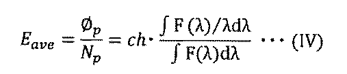
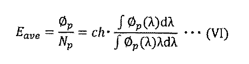

Eedgeの算出方法について説明する。図2は図1で用いた発光中心物質の短波長側の発光端付近を拡大した図である。Eedgeは図2のように、発光スペクトルF(λ)の短波長側の裾において、半値付近で接線を引き、その接線とx軸の交点から求めることができる。
図3は、図1および図2で用いた発光物質を発光中心とし、マイクロキャビティ構造を有する有機EL素子(トップエミッション)に関し、EemとEQEとの関係、およびEemとBIとの関係を調査したものである。なお、ここでのEQEは、正面輝度からランバーシアン配光を仮定して算出した未補正EQEである。また、輝度が1000cd/m2付近の時のEQEを用いている。
(但し、Eaveは発光素子に用いられている発光中心物質のトルエン溶液における発光の平均フォトンエネルギー(単位[eV])を表し、Eedgeは発光中心物質のトルエン溶液におけるPL発光スペクトルの短波長側の発光端エネルギー(単位[eV])を表し、EemはEL発光ピークエネルギー(単位[eV])を表すものとする。)


本実施の形態では、実施の形態1に記載の発光素子を用いた発光装置について説明する。
本実施の形態では、実施の形態1に記載の発光素子を照明装置として用いる例を図6を参照しながら説明する。図6(B)は照明装置の上面図、図6(A)は図6(B)におけるe−f断面図である。
本実施の形態では、実施の形態1に記載の発光素子をその一部に含む電子機器の例について説明する。実施の形態1に記載の発光素子は発光効率が良好であり、消費電力の小さい発光素子である。その結果、本実施の形態に記載の電子機器は、消費電力が小さい発光部を有する電子機器とすることが可能である。

まず、ガラス基板上に、反射電極として、銀(Ag)とパラジウム(Pd)と銅(Cu)の合金膜(Ag−Pd−Cu(APC)膜)をスパッタリング法により、100nmの膜厚で成膜した後、透明電極として酸化珪素を含むインジウム錫酸化物(ITSO)をスパッタリング法により、85nmの膜厚で成膜して第1の電極101を形成した。なお、その電極面積は4mm2(2mm×2mm)とした。

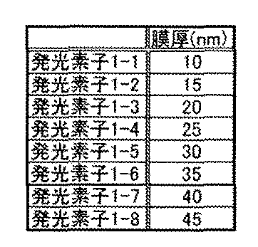

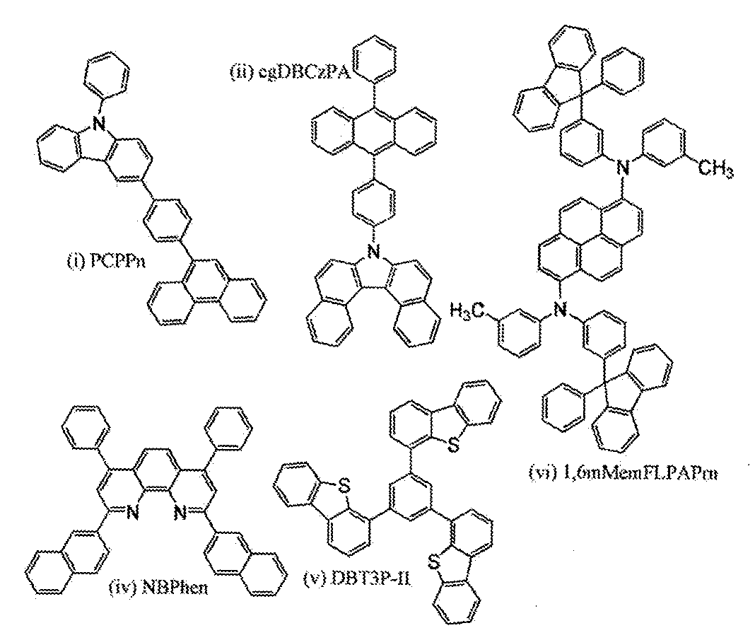
まず、ガラス基板上に、反射電極として、銀(Ag)とパラジウム(Pd)と銅(Cu)の合金膜(Ag−Pd−Cu(APC)膜)をスパッタリング法により、100nmの膜厚で成膜した後、透明電極として酸化珪素を含むインジウム錫酸化物(ITSO)をスパッタリング法により、85nmの膜厚で成膜して第1の電極101を形成した。なお、その電極面積は4mm2(2mm×2mm)とした。

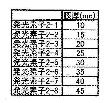

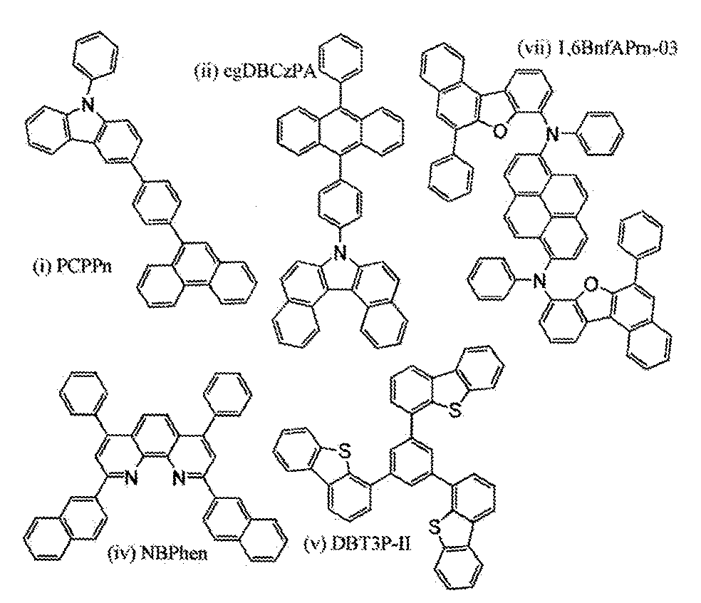
まず、ガラス基板上に、反射電極として、銀(Ag)とパラジウム(Pd)と銅(Cu)の合金膜(Ag−Pd−Cu(APC)膜)をスパッタリング法により、100nmの膜厚で成膜した後、透明電極として酸化珪素を含むインジウム錫酸化物(ITSO)をスパッタリング法により、95nmの膜厚で成膜して第1の電極101を形成した。なお、その電極面積は4mm2(2mm×2mm)とした。

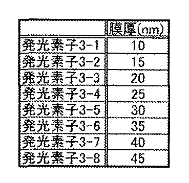


まず、ガラス基板上に、透明電極として酸化珪素を含むインジウム錫酸化物(ITSO)を70nmの膜厚で形成した後、半透過・半反射電極として、銀(Ag)とパラジウム(Pd)と銅(Cu)の合金膜(Ag−Pd−Cu(APC)膜)をスパッタリング法により、膜厚25nmとなるように成膜した後、さらに透明電極としてITSOをスパッタリング法により、10nmの膜厚で成膜して第1の電極101を形成した。なお、その電極面積は4mm2(2mm×2mm)とした。


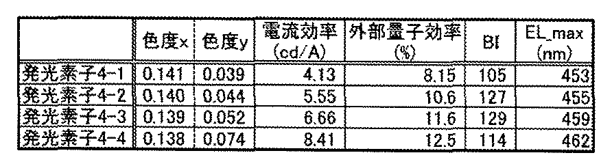
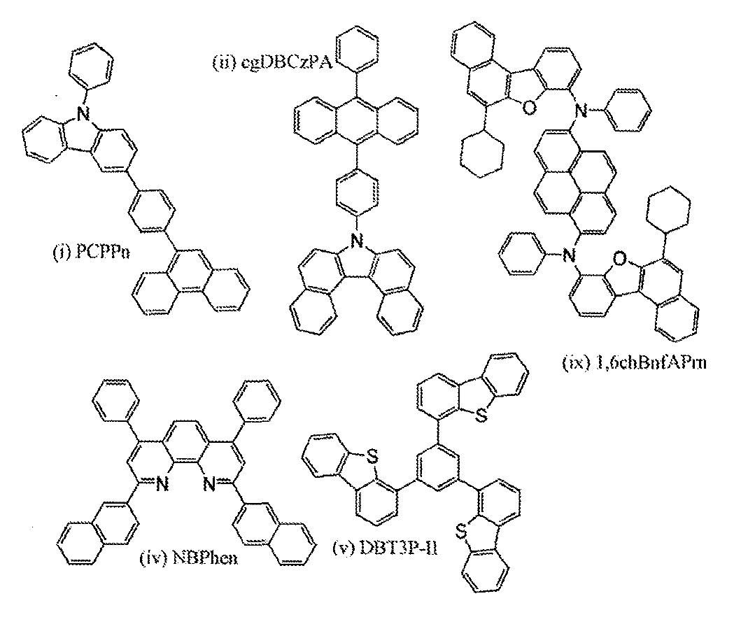
まず、ガラス基板上に、反射電極として、銀(Ag)とパラジウム(Pd)と銅(Cu)の合金膜(Ag−Pd−Cu(APC)膜)をスパッタリング法により、100nmの膜厚で成膜した後、透明電極として酸化珪素を含むインジウム錫酸化物(ITSO)をスパッタリング法により、85nmの膜厚で成膜して第1の電極101を形成した。なお、その電極面積は4mm2(2mm×2mm)とした。


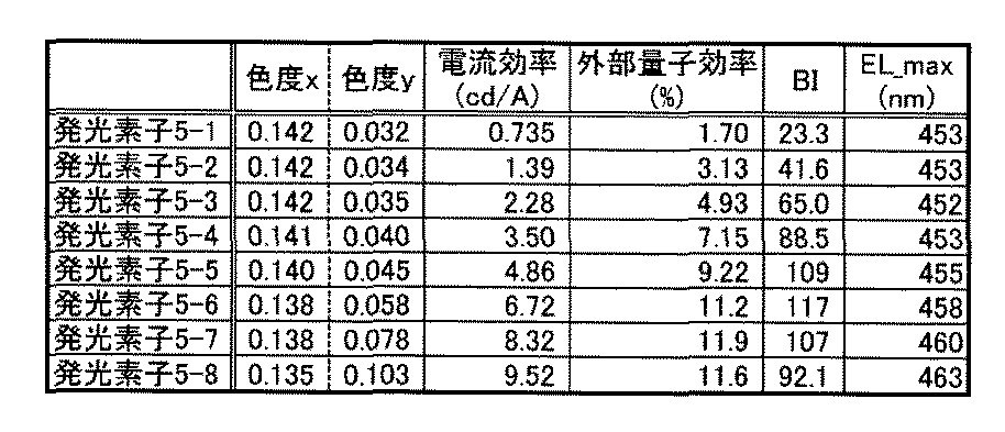
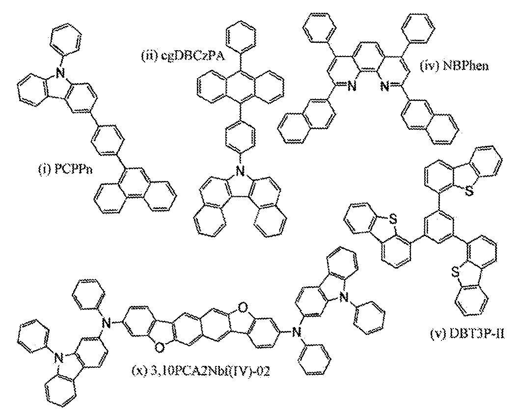
まず、ガラス基板上に、反射電極として、銀(Ag)とパラジウム(Pd)と銅(Cu)の合金膜(Ag−Pd−Cu(APC)膜)をスパッタリング法により、100nmの膜厚で成膜した後、透明電極として酸化珪素を含むインジウム錫酸化物(ITSO)をスパッタリング法により、85nmの膜厚で成膜して第1の電極101を形成した。なお、その電極面積は4mm2(2mm×2mm)とした。


まず、ガラス基板上に、反射電極として、銀(Ag)とパラジウム(Pd)と銅(Cu)の合金膜(Ag−Pd−Cu(APC)膜)をスパッタリング法により、100nmの膜厚で成膜した後、透明電極として酸化珪素を含むインジウム錫酸化物(ITSO)をスパッタリング法により、85nmの膜厚で成膜して第1の電極101を形成した。なお、その電極面積は4mm2(2mm×2mm)とした。
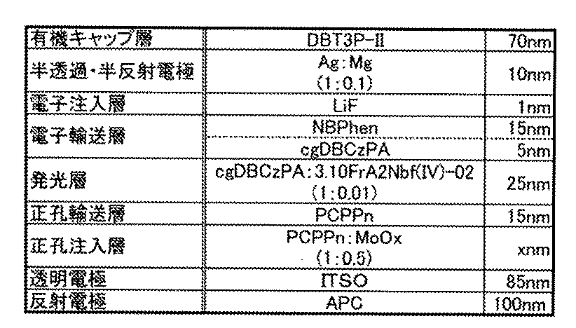
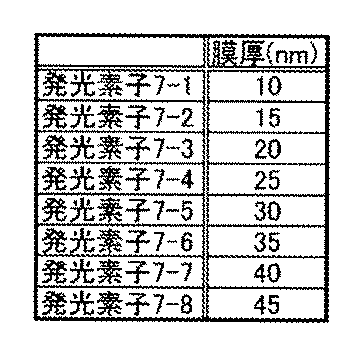

Claims (11)
- 第1の電極と、
第2の電極と、
前記第1の電極と前記第2の電極との間に挟まれたEL層とを有し、
前記第1の電極および前記第2の電極の一方が反射電極、他方が半透過半反射電極である発光素子において、
前記EL層は発光中心物質を有し、
前記発光中心物質が溶液状態において発する光のフォトンエネルギーの平均値をEave[eV]とし、前記発光中心物質の前記溶液状態における発光スペクトルの短波長側の発光端エネルギーをEedge[eV]とすると、前記発光素子から発する光のピーク波長のフォトンエネルギーEem[eV]が、下記式(1)で表される発光素子。

- 第1の電極と、
第2の電極と、
前記第1の電極と前記第2の電極との間に挟まれたEL層とを有し、
前記第1の電極および前記第2の電極の一方が、反射電極、他方が半透過半反射電極である発光素子において、
前記EL層は、発光中心物質を有し、
前記発光中心物質が発する光のフォトンエネルギーの平均値をEave[eV]とし、前記発光中心物質の発光スペクトルの短波長側の発光端エネルギーをEedge[eV]とすると、前記発光素子から発する光のピーク波長のフォトンエネルギーEem[eV]が、下記式(1)で表される発光素子。

- 請求項1において、前記発光中心物質が青色発光を呈する発光素子。
- 第1の電極と、
第2の電極と、
前記第1の電極と前記第2の電極との間に挟まれたEL層とを有し、
前記第1の電極及び前記第2の電極の一方が反射電極、他方が半透過半反射電極である発光素子において、
前記EL層は青色発光を呈する発光中心物質を有し、
前記発光中心物質が発する光のフォトンエネルギーの平均値をEave[eV]とし、前記発光中心物質の発光スペクトルの短波長側の発光端エネルギーをEedge[eV]とすると、前記発光素子から発する光のピーク波長のフォトンエネルギーEem[eV]が、下記式(2)で表される発光素子。

- 請求項3または請求項4において、前記Eemが2.6eV以上2.9eV以下である発光素子。
- 請求項1乃至請求項5のいずれか一項において、前記半透過半反射電極における、前記反射電極に対する面と反対の面には、分子量300以上1200以下の有機化合物層が形成されている発光素子。
- 請求項2乃至請求項6のいずれか一項において、前記Eaveおよび前記Eedgeは室温における比誘電率が1以上10以下の溶媒中で測定される、発光素子。
- 請求項1において、前記溶液状態における溶媒がトルエンまたはクロロホルムである発光素子。
- 請求項1乃至請求項7に記載の発光素子と、トランジスタ、または、基板と、を有する発光装置。
- 請求項8に記載の発光装置と、センサ、操作ボタン、スピーカ、または、マイクと、
を有する電子機器。 - 請求項8に記載の発光装置と、筐体と、を有する照明装置。
Priority Applications (9)
| Application Number | Priority Date | Filing Date | Title |
|---|---|---|---|
| CN201980033542.XA CN112424969A (zh) | 2018-05-18 | 2019-05-10 | 发光元件、发光装置、电子设备及照明装置 |
| KR1020207036304A KR102809218B1 (ko) | 2018-05-18 | 2019-05-10 | 발광 소자, 발광 장치, 전자 기기, 및 조명 장치 |
| KR1020257015675A KR20250069709A (ko) | 2018-05-18 | 2019-05-10 | 발광 소자, 발광 장치, 전자 기기, 및 조명 장치 |
| JP2020519209A JPWO2019220283A1 (ja) | 2018-05-18 | 2019-05-10 | 発光素子、発光装置、電子機器および照明装置 |
| US17/055,933 US11917840B2 (en) | 2018-05-18 | 2019-05-10 | Light-emitting device with reflective electrode and light-emitting layer |
| US18/586,676 US12382782B2 (en) | 2018-05-18 | 2024-02-26 | Estimation of cavity length of light-emitting device |
| JP2024065107A JP2024083574A (ja) | 2018-05-18 | 2024-04-15 | 発光素子、発光装置、電子機器および照明装置 |
| US19/203,242 US20250280652A1 (en) | 2018-05-18 | 2025-05-09 | Light-emitting device, light-emitting apparatus, electronic device, and lighting device |
| JP2025196514A JP2026020219A (ja) | 2018-05-18 | 2025-11-17 | 発光素子 |
Applications Claiming Priority (2)
| Application Number | Priority Date | Filing Date | Title |
|---|---|---|---|
| JP2018096504 | 2018-05-18 | ||
| JP2018-096504 | 2018-05-18 |
Related Child Applications (2)
| Application Number | Title | Priority Date | Filing Date |
|---|---|---|---|
| US17/055,933 A-371-Of-International US11917840B2 (en) | 2018-05-18 | 2019-05-10 | Light-emitting device with reflective electrode and light-emitting layer |
| US18/586,676 Continuation US12382782B2 (en) | 2018-05-18 | 2024-02-26 | Estimation of cavity length of light-emitting device |
Publications (1)
| Publication Number | Publication Date |
|---|---|
| WO2019220283A1 true WO2019220283A1 (ja) | 2019-11-21 |
Family
ID=68539862
Family Applications (1)
| Application Number | Title | Priority Date | Filing Date |
|---|---|---|---|
| PCT/IB2019/053851 Ceased WO2019220283A1 (ja) | 2018-05-18 | 2019-05-10 | 発光素子、発光装置、電子機器および照明装置 |
Country Status (6)
| Country | Link |
|---|---|
| US (3) | US11917840B2 (ja) |
| JP (3) | JPWO2019220283A1 (ja) |
| KR (2) | KR102809218B1 (ja) |
| CN (1) | CN112424969A (ja) |
| TW (3) | TW202602328A (ja) |
| WO (1) | WO2019220283A1 (ja) |
Cited By (4)
| Publication number | Priority date | Publication date | Assignee | Title |
|---|---|---|---|---|
| US10763441B2 (en) | 2018-10-09 | 2020-09-01 | Idemitsu Kosan Co., Ltd. | Organic electroluminescence device and electronic apparatus provided with the same |
| EP3940807A1 (en) * | 2020-07-17 | 2022-01-19 | Samsung Display Co., Ltd. | Light emitting device and electronic apparatus including same |
| US12171141B2 (en) | 2018-10-09 | 2024-12-17 | Idemitsu Kosan Co., Ltd. | Organic electroluminescence device and electronic apparatus provided with the same |
| US12433162B2 (en) | 2018-10-09 | 2025-09-30 | Idemitsu Kosan Co., Ltd. | Compound, organic electroluminescence device, and electronic apparatus |
Families Citing this family (6)
| Publication number | Priority date | Publication date | Assignee | Title |
|---|---|---|---|---|
| TWI747382B (zh) * | 2020-07-15 | 2021-11-21 | 友達光電股份有限公司 | 發光裝置 |
| US12349538B2 (en) | 2021-03-25 | 2025-07-01 | Semiconductor Energy Laboratory Co., Ltd. | Light-emitting device, display device, light-emitting apparatus, electronic device, and lighting device |
| KR20230000968A (ko) | 2021-06-25 | 2023-01-03 | 가부시키가이샤 한도오따이 에네루기 켄큐쇼 | 발광 디바이스, 표시 장치, 발광 장치, 전자 기기, 및 조명 장치 |
| KR102911765B1 (ko) * | 2021-08-25 | 2026-01-15 | 삼성디스플레이 주식회사 | 발광 소자 및 이를 포함하는 표시 장치 |
| US20240357855A1 (en) * | 2022-04-24 | 2024-10-24 | Beijing Boe Technology Development Co., Ltd. | Quantum dot light emitting diode, manufacturing method thereof and display panel |
| WO2024087228A1 (zh) * | 2022-10-28 | 2024-05-02 | 京东方科技集团股份有限公司 | 发光器件及其制备方法、显示基板 |
Citations (4)
| Publication number | Priority date | Publication date | Assignee | Title |
|---|---|---|---|---|
| JP2010287524A (ja) * | 2009-06-15 | 2010-12-24 | Sony Corp | 表示素子および表示装置 |
| WO2011043083A1 (ja) * | 2009-10-09 | 2011-04-14 | 出光興産株式会社 | 有機エレクトロルミネッセンス素子 |
| JP2012018939A (ja) * | 2011-10-25 | 2012-01-26 | Pioneer Electronic Corp | 発光素子 |
| JP2015173263A (ja) * | 2014-02-21 | 2015-10-01 | 株式会社半導体エネルギー研究所 | 有機化合物、発光素子、ディスプレイモジュール、照明モジュール、発光装置、表示装置、電子機器及び照明装置 |
Family Cites Families (139)
| Publication number | Priority date | Publication date | Assignee | Title |
|---|---|---|---|---|
| JPS60218626A (ja) | 1984-04-13 | 1985-11-01 | Sharp Corp | カラ−液晶表示装置 |
| JP2797883B2 (ja) | 1993-03-18 | 1998-09-17 | 株式会社日立製作所 | 多色発光素子とその基板 |
| JP2821347B2 (ja) | 1993-10-12 | 1998-11-05 | 日本電気株式会社 | 電流制御型発光素子アレイ |
| JP2846571B2 (ja) | 1994-02-25 | 1999-01-13 | 出光興産株式会社 | 有機エレクトロルミネッセンス素子 |
| US5780174A (en) | 1995-10-27 | 1998-07-14 | Kabushiki Kaisha Toyota Chuo Kenkyusho | Micro-optical resonator type organic electroluminescent device |
| JP4477150B2 (ja) | 1996-01-17 | 2010-06-09 | 三星モバイルディスプレイ株式會社 | 有機薄膜el素子 |
| US6091195A (en) | 1997-02-03 | 2000-07-18 | The Trustees Of Princeton University | Displays having mesa pixel configuration |
| JPH10270171A (ja) | 1997-01-27 | 1998-10-09 | Junji Kido | 有機エレクトロルミネッセント素子 |
| US5989737A (en) | 1997-02-27 | 1999-11-23 | Xerox Corporation | Organic electroluminescent devices |
| JPH11251067A (ja) | 1998-03-02 | 1999-09-17 | Junji Kido | 有機エレクトロルミネッセント素子 |
| JP5358050B2 (ja) | 1998-06-26 | 2013-12-04 | 出光興産株式会社 | 発光装置 |
| US6140764A (en) | 1998-07-20 | 2000-10-31 | Motorola, Inc. | Organic electroluminescent apparatus with mircrocavity |
| US6384529B2 (en) | 1998-11-18 | 2002-05-07 | Eastman Kodak Company | Full color active matrix organic electroluminescent display panel having an integrated shadow mask |
| JP4001692B2 (ja) | 1999-02-18 | 2007-10-31 | パイオニア株式会社 | 有機エレクトロルミネッセンス素子とその製造方法 |
| US6366025B1 (en) | 1999-02-26 | 2002-04-02 | Sanyo Electric Co., Ltd. | Electroluminescence display apparatus |
| JP4136185B2 (ja) | 1999-05-12 | 2008-08-20 | パイオニア株式会社 | 有機エレクトロルミネッセンス多色ディスプレイ及びその製造方法 |
| JP2000340366A (ja) | 1999-05-27 | 2000-12-08 | Tdk Corp | 発光ダイオード |
| JP2001043980A (ja) | 1999-07-29 | 2001-02-16 | Sony Corp | 有機エレクトロルミネッセンス素子及び表示装置 |
| JP2001052866A (ja) | 1999-08-05 | 2001-02-23 | Fuji Electric Co Ltd | 蛍光変換フィルタ及び該フィルタを備えた有機発光素子 |
| GB2353400B (en) | 1999-08-20 | 2004-01-14 | Cambridge Display Tech Ltd | Mutiple-wavelength light emitting device and electronic apparatus |
| KR20010050711A (ko) | 1999-09-29 | 2001-06-15 | 준지 키도 | 유기전계발광소자, 유기전계발광소자그룹 및 이런소자들의 발광스펙트럼의 제어방법 |
| TW478019B (en) | 1999-10-29 | 2002-03-01 | Semiconductor Energy Lab | Self light-emitting device |
| JP4174989B2 (ja) | 1999-11-22 | 2008-11-05 | ソニー株式会社 | 表示装置 |
| KR20010085420A (ko) | 2000-02-23 | 2001-09-07 | 기타지마 요시토시 | 전계발광소자와 그 제조방법 |
| US7579203B2 (en) | 2000-04-25 | 2009-08-25 | Semiconductor Energy Laboratory Co., Ltd. | Light emitting device |
| US6680570B2 (en) | 2001-03-21 | 2004-01-20 | Agilent Technologies, Inc. | Polymer organic light emitting device with improved color control |
| JP2002359076A (ja) | 2001-03-27 | 2002-12-13 | Konica Corp | 有機エレクトロルミネッセンス素子、表示装置、発光方法、表示方法および透明基板 |
| JP3508741B2 (ja) | 2001-06-05 | 2004-03-22 | ソニー株式会社 | 表示素子 |
| JP3804858B2 (ja) | 2001-08-31 | 2006-08-02 | ソニー株式会社 | 有機電界発光素子およびその製造方法 |
| JP2003109775A (ja) | 2001-09-28 | 2003-04-11 | Sony Corp | 有機電界発光素子 |
| JP2003234186A (ja) | 2001-12-06 | 2003-08-22 | Sony Corp | 表示装置およびその製造方法 |
| KR100490535B1 (ko) | 2001-12-17 | 2005-05-17 | 삼성에스디아이 주식회사 | 유기 전계발광 소자 |
| JP3933591B2 (ja) | 2002-03-26 | 2007-06-20 | 淳二 城戸 | 有機エレクトロルミネッセント素子 |
| JP4240276B2 (ja) | 2002-07-05 | 2009-03-18 | 株式会社半導体エネルギー研究所 | 発光装置 |
| US20060183625A1 (en) | 2002-07-09 | 2006-08-17 | Kenichiro Miyahara | Substrate for forming thin film, thin film substrate, optical wave guide, luminescent element and substrate for carrying luminescent element |
| JP2004055461A (ja) | 2002-07-23 | 2004-02-19 | Seiko Epson Corp | 発光装置及びその製造方法、並びに電子機器 |
| KR100711161B1 (ko) | 2002-09-12 | 2007-04-24 | 도시바 마쯔시따 디스플레이 테크놀로지 컴퍼니, 리미티드 | 유기 el 디스플레이 |
| US7158161B2 (en) | 2002-09-20 | 2007-01-02 | Matsushita Electric Industrial Co., Ltd. | Organic electroluminescence element and an exposure unit and image-forming apparatus both using the element |
| JP2004119304A (ja) | 2002-09-27 | 2004-04-15 | Sanyo Electric Co Ltd | 有機エレクトロルミネッセンス表示装置およびその製造方法 |
| JP3703028B2 (ja) | 2002-10-04 | 2005-10-05 | ソニー株式会社 | 表示素子およびこれを用いた表示装置 |
| JP4343511B2 (ja) | 2002-10-08 | 2009-10-14 | キヤノン株式会社 | 多色発光素子 |
| TWI352553B (en) | 2002-12-26 | 2011-11-11 | Semiconductor Energy Lab | Light emitting device and a method for manufacturi |
| US6956323B2 (en) | 2003-02-20 | 2005-10-18 | Fuji Electric Co., Ltd. | Color conversion filter substrate and organic multicolor light emitting device |
| JP4526776B2 (ja) | 2003-04-02 | 2010-08-18 | 株式会社半導体エネルギー研究所 | 発光装置及び電子機器 |
| KR100527187B1 (ko) | 2003-05-01 | 2005-11-08 | 삼성에스디아이 주식회사 | 고효율 유기전계 발광표시장치 및 그의 제조방법 |
| JP2005044778A (ja) | 2003-07-19 | 2005-02-17 | Samsung Sdi Co Ltd | 電界発光素子 |
| KR20050015902A (ko) | 2003-08-14 | 2005-02-21 | 엘지전자 주식회사 | 유기 el 소자 및 그 제조방법 |
| US7030553B2 (en) | 2003-08-19 | 2006-04-18 | Eastman Kodak Company | OLED device having microcavity gamut subpixels and a within gamut subpixel |
| JP4823478B2 (ja) | 2003-09-19 | 2011-11-24 | 株式会社半導体エネルギー研究所 | 発光装置の作製方法 |
| JP4016144B2 (ja) | 2003-09-19 | 2007-12-05 | ソニー株式会社 | 有機発光素子およびその製造方法ならびに表示装置 |
| EP2509397B1 (en) | 2003-09-19 | 2018-12-05 | Sony Corporation | Display unit with resonator structure |
| JP4325343B2 (ja) | 2003-09-25 | 2009-09-02 | セイコーエプソン株式会社 | 膜形成方法およびデバイス製造方法 |
| KR101286219B1 (ko) | 2003-09-26 | 2013-07-15 | 가부시키가이샤 한도오따이 에네루기 켄큐쇼 | 발광소자의 제조방법 |
| JP4428979B2 (ja) | 2003-09-30 | 2010-03-10 | 三洋電機株式会社 | 有機elパネル |
| JP4895490B2 (ja) | 2003-09-30 | 2012-03-14 | 三洋電機株式会社 | 有機elパネル |
| US7541734B2 (en) | 2003-10-03 | 2009-06-02 | Semiconductor Energy Laboratory Co., Ltd. | Light emitting device having a layer with a metal oxide and a benzoxazole derivative |
| JP4476594B2 (ja) | 2003-10-17 | 2010-06-09 | 淳二 城戸 | 有機エレクトロルミネッセント素子 |
| JP4683829B2 (ja) | 2003-10-17 | 2011-05-18 | 淳二 城戸 | 有機エレクトロルミネッセント素子及びその製造方法 |
| JP4243237B2 (ja) | 2003-11-10 | 2009-03-25 | 淳二 城戸 | 有機素子、有機el素子、有機太陽電池、及び、有機fet構造、並びに、有機素子の製造方法 |
| JP4300176B2 (ja) | 2003-11-13 | 2009-07-22 | ローム株式会社 | 有機エレクトロルミネッセント素子 |
| ATE433200T1 (de) | 2003-12-16 | 2009-06-15 | Panasonic Corp | Organisches elektrolumineszenzbauelement und herstellungsverfahren dafür |
| CN101673808B (zh) | 2003-12-26 | 2012-05-23 | 株式会社半导体能源研究所 | 发光元件 |
| US7792489B2 (en) | 2003-12-26 | 2010-09-07 | Semiconductor Energy Laboratory Co., Ltd. | Light emitting device, electronic appliance, and method for manufacturing light emitting device |
| JP4439260B2 (ja) | 2003-12-26 | 2010-03-24 | 三洋電機株式会社 | 表示装置の製造方法 |
| JP2005197009A (ja) | 2003-12-26 | 2005-07-21 | Sanyo Electric Co Ltd | 表示装置及びその製造方法及び製造装置 |
| US7019331B2 (en) | 2004-01-22 | 2006-03-28 | Eastman Kodak Company | Green light-emitting microcavity OLED device using a yellow color filter element |
| JP4689176B2 (ja) | 2004-02-26 | 2011-05-25 | 大日本印刷株式会社 | 有機エレクトロルミネッセンス素子 |
| WO2005091321A1 (en) | 2004-03-15 | 2005-09-29 | Aerospace Optics, Inc. | Programmable dichromatic legend lighted switches |
| US7157156B2 (en) | 2004-03-19 | 2007-01-02 | Eastman Kodak Company | Organic light emitting device having improved stability |
| JP2005270725A (ja) | 2004-03-23 | 2005-10-06 | Sharp Corp | パターン基板、パターン基板の製造方法、及びパターン基板の製造装置 |
| US7223641B2 (en) | 2004-03-26 | 2007-05-29 | Semiconductor Energy Laboratory Co., Ltd. | Semiconductor device, method for manufacturing the same, liquid crystal television and EL television |
| JP2005317506A (ja) | 2004-03-31 | 2005-11-10 | Sanyo Electric Co Ltd | 有機エレクトロルミネッセンス表示装置 |
| US7129634B2 (en) | 2004-04-07 | 2006-10-31 | Eastman Kodak Company | Color OLED with added color gamut pixels |
| US7057339B2 (en) | 2004-04-08 | 2006-06-06 | Eastman Kodak Company | OLED with color change media |
| US7247394B2 (en) | 2004-05-04 | 2007-07-24 | Eastman Kodak Company | Tuned microcavity color OLED display |
| US7023013B2 (en) | 2004-06-16 | 2006-04-04 | Eastman Kodak Company | Array of light-emitting OLED microcavity pixels |
| US7196469B2 (en) | 2004-06-18 | 2007-03-27 | Eastman Kodak Company | Reducing undesirable absorption in a microcavity OLED |
| TWI272039B (en) | 2004-06-18 | 2007-01-21 | Sanyo Electric Co | Electroluminescence panel |
| KR100611756B1 (ko) | 2004-06-18 | 2006-08-10 | 삼성에스디아이 주식회사 | 유기 전계 발광 소자 및 그의 제조 방법 |
| US7554265B2 (en) | 2004-06-25 | 2009-06-30 | Semiconductor Energy Laboratory Co., Ltd. | Display device |
| JP4925569B2 (ja) | 2004-07-08 | 2012-04-25 | ローム株式会社 | 有機エレクトロルミネッセント素子 |
| KR100721554B1 (ko) | 2004-07-22 | 2007-05-23 | 삼성에스디아이 주식회사 | 유기 전계 발광 소자 및 그의 제조 방법 |
| JP2006295104A (ja) | 2004-07-23 | 2006-10-26 | Semiconductor Energy Lab Co Ltd | 発光素子およびそれを用いた発光装置 |
| EP1624502B1 (en) | 2004-08-04 | 2015-11-18 | Semiconductor Energy Laboratory Co., Ltd. | Light-emitting element, display device, and electronic appliance |
| US7601988B2 (en) | 2004-09-24 | 2009-10-13 | Semiconductor Energy Laboratory Co., Ltd. | Light emitting device |
| US8008652B2 (en) | 2004-09-24 | 2011-08-30 | Semiconductor Energy Laboratory Co., Ltd. | Light emitting device |
| US7753751B2 (en) | 2004-09-29 | 2010-07-13 | Semiconductor Energy Laboratory Co., Ltd. | Method of fabricating the display device |
| US7737626B2 (en) | 2004-09-30 | 2010-06-15 | Semiconductor Energy Laboratory Co., Ltd. | Light emitting element |
| KR100685407B1 (ko) | 2004-10-18 | 2007-02-22 | 삼성에스디아이 주식회사 | 레드, 그린, 블루, 시안, 마젠타 및 옐로우칼라조절층들을 갖는 풀칼라 유기전계발광표시장치 |
| US8202630B2 (en) | 2004-11-05 | 2012-06-19 | Semiconductor Energy Laboratory Co., Ltd. | Light emitting element and light emitting device using the same |
| WO2006049323A1 (en) | 2004-11-05 | 2006-05-11 | Semiconductor Energy Laboratory Co., Ltd. | Light-emitting element and light emitting device using the same |
| US7304428B2 (en) | 2004-12-14 | 2007-12-04 | Eastman Kodak Company | Multilayered cathode structures having silver for OLED devices |
| US8633473B2 (en) | 2004-12-28 | 2014-01-21 | Semiconductor Energy Laboratory Co., Ltd. | High contrast light emitting device and method for manufacturing the same |
| US8569948B2 (en) | 2004-12-28 | 2013-10-29 | Samsung Display Co., Ltd. | Electroluminescent devices and methods of making electroluminescent devices including an optical spacer |
| JP4939809B2 (ja) | 2005-01-21 | 2012-05-30 | 株式会社半導体エネルギー研究所 | 発光装置 |
| US7851989B2 (en) | 2005-03-25 | 2010-12-14 | Semiconductor Energy Laboratory Co., Ltd. | Light emitting device |
| US7564181B2 (en) | 2005-04-08 | 2009-07-21 | Eastman Kodak Company | Performance enhancement layer for OLED devices |
| US7271537B2 (en) | 2005-04-15 | 2007-09-18 | Sony Corporation | Display device and a method of manufacturing the display device |
| US8269227B2 (en) | 2005-06-09 | 2012-09-18 | Semiconductor Energy Laboratory Co., Ltd. | Light emitting device and electronic device |
| US8729795B2 (en) | 2005-06-30 | 2014-05-20 | Semiconductor Energy Laboratory Co., Ltd. | Light emitting device and electronic device |
| KR20070019495A (ko) | 2005-08-12 | 2007-02-15 | 삼성에스디아이 주식회사 | 백색 유기 발광 소자 및 그의 제조방법 |
| US20070058182A1 (en) | 2005-08-30 | 2007-03-15 | Texas Instruments Incorporated | Multiple spatial light modulators in a package |
| EP1770676B1 (en) | 2005-09-30 | 2017-05-03 | Semiconductor Energy Laboratory Co., Ltd. | Display device and electronic device |
| EP1863105B1 (en) | 2006-06-02 | 2020-02-19 | Semiconductor Energy Laboratory Co., Ltd. | Light-emitting element, light-emitting device, and electronic device |
| US7741770B2 (en) | 2007-10-05 | 2010-06-22 | Global Oled Technology Llc | LED device having improved light output |
| JP4895145B2 (ja) | 2009-08-20 | 2012-03-14 | 株式会社デンソー | 車両用回転電機 |
| KR101058109B1 (ko) | 2009-09-15 | 2011-08-24 | 삼성모바일디스플레이주식회사 | 유기 발광 디스플레이 장치 |
| KR101321878B1 (ko) | 2009-09-25 | 2013-10-28 | 엘지디스플레이 주식회사 | 유기전계 발광소자 |
| CN102474938B (zh) | 2009-09-29 | 2015-09-09 | 株式会社日本有机雷特显示器 | 发光元件以及使用该发光元件的显示装置 |
| JP5676867B2 (ja) | 2009-09-29 | 2015-02-25 | 住友化学株式会社 | 有機エレクトロルミネッセンス素子 |
| TWI525377B (zh) | 2010-01-24 | 2016-03-11 | 半導體能源研究所股份有限公司 | 顯示裝置 |
| JP5407907B2 (ja) | 2010-01-29 | 2014-02-05 | ソニー株式会社 | 発光素子、照明装置および表示装置 |
| JP5407910B2 (ja) | 2010-01-29 | 2014-02-05 | ソニー株式会社 | 発光装置、照明装置および表示装置 |
| KR101894898B1 (ko) | 2011-02-11 | 2018-09-04 | 가부시키가이샤 한도오따이 에네루기 켄큐쇼 | 발광 장치 및 발광 장치를 사용한 전자 기기 |
| JP5996876B2 (ja) | 2011-02-11 | 2016-09-21 | 株式会社半導体エネルギー研究所 | 発光素子及び表示装置 |
| US8957442B2 (en) | 2011-02-11 | 2015-02-17 | Semiconductor Energy Laboratory Co., Ltd. | Light-emitting device and display device |
| KR101880183B1 (ko) | 2011-02-11 | 2018-07-19 | 가부시키가이샤 한도오따이 에네루기 켄큐쇼 | 발광 장치 및 표시 장치 |
| TWI562424B (en) | 2011-03-25 | 2016-12-11 | Semiconductor Energy Lab Co Ltd | Light-emitting panel, light-emitting device, and method for manufacturing the light-emitting panel |
| US8884316B2 (en) | 2011-06-17 | 2014-11-11 | Universal Display Corporation | Non-common capping layer on an organic device |
| KR101953724B1 (ko) | 2011-08-26 | 2019-03-04 | 가부시키가이샤 한도오따이 에네루기 켄큐쇼 | 발광 모듈, 발광 장치, 발광 모듈의 제작 방법, 발광 장치의 제작 방법 |
| US9123667B2 (en) | 2011-10-04 | 2015-09-01 | Universal Display Corporation | Power-efficient RGBW OLED display |
| KR20130049728A (ko) | 2011-11-04 | 2013-05-14 | 가부시키가이샤 한도오따이 에네루기 켄큐쇼 | 발광 모듈 및 발광 장치 |
| US9711110B2 (en) | 2012-04-06 | 2017-07-18 | Semiconductor Energy Laboratory Co., Ltd. | Display device comprising grayscale conversion portion and display portion |
| US9793444B2 (en) | 2012-04-06 | 2017-10-17 | Semiconductor Energy Laboratory Co., Ltd. | Display device and electronic device |
| KR20150082388A (ko) | 2012-10-30 | 2015-07-15 | 가부시키가이샤 한도오따이 에네루기 켄큐쇼 | 발광 패널, 디스플레이 장치, 및 발광 패널을 제작하는 방법 |
| US9385168B2 (en) | 2013-01-18 | 2016-07-05 | Universal Display Corporation | High resolution low power consumption OLED display with extended lifetime |
| US10243023B2 (en) | 2013-01-18 | 2019-03-26 | Universal Display Corporation | Top emission AMOLED displays using two emissive layers |
| JP6099420B2 (ja) | 2013-02-08 | 2017-03-22 | 株式会社半導体エネルギー研究所 | 発光装置 |
| JP6174877B2 (ja) | 2013-03-21 | 2017-08-02 | 株式会社半導体エネルギー研究所 | 表示装置及び電子機器 |
| JP6114592B2 (ja) | 2013-03-21 | 2017-04-12 | 株式会社半導体エネルギー研究所 | 表示装置およびその製造方法、電子機器 |
| US9224980B2 (en) | 2013-03-28 | 2015-12-29 | Semiconductor Energy Laboratory Co., Ltd. | Light-emitting device |
| US9246133B2 (en) | 2013-04-12 | 2016-01-26 | Semiconductor Energy Laboratory Co., Ltd. | Light-emitting module, light-emitting panel, and light-emitting device |
| KR102265675B1 (ko) | 2013-05-20 | 2021-06-15 | 가부시키가이샤 한도오따이 에네루기 켄큐쇼 | 유기 금속 착체, 발광 소자, 발광 장치, 전자기기, 및 조명 장치 |
| CN103646957B (zh) | 2013-11-18 | 2015-08-19 | 上海和辉光电有限公司 | 一种oled显示面板以及用于该oled显示面板的蓝光滤除方法 |
| TWI606623B (zh) | 2014-01-10 | 2017-11-21 | 樂金顯示科技股份有限公司 | 有機發光裝置及照明設備 |
| WO2015132693A1 (en) | 2014-03-07 | 2015-09-11 | Semiconductor Energy Laboratory Co., Ltd. | Light-emitting element, light-emitting device, electronic device, and lighting device |
| JP2015187982A (ja) | 2014-03-13 | 2015-10-29 | 株式会社半導体エネルギー研究所 | 発光素子、発光装置、電子機器、および照明装置 |
| KR102377032B1 (ko) * | 2015-10-31 | 2022-03-18 | 엘지디스플레이 주식회사 | 유기 발광 표시 장치 |
| KR102465177B1 (ko) | 2015-11-17 | 2022-11-08 | 엘지디스플레이 주식회사 | 유기 발광 표시 장치 |
-
2019
- 2019-05-10 US US17/055,933 patent/US11917840B2/en active Active
- 2019-05-10 CN CN201980033542.XA patent/CN112424969A/zh active Pending
- 2019-05-10 KR KR1020207036304A patent/KR102809218B1/ko active Active
- 2019-05-10 WO PCT/IB2019/053851 patent/WO2019220283A1/ja not_active Ceased
- 2019-05-10 KR KR1020257015675A patent/KR20250069709A/ko active Pending
- 2019-05-10 JP JP2020519209A patent/JPWO2019220283A1/ja not_active Withdrawn
- 2019-05-16 TW TW114135851A patent/TW202602328A/zh unknown
- 2019-05-16 TW TW108116854A patent/TWI860997B/zh active
- 2019-05-16 TW TW113138218A patent/TWI902488B/zh active
-
2024
- 2024-02-26 US US18/586,676 patent/US12382782B2/en active Active
- 2024-04-15 JP JP2024065107A patent/JP2024083574A/ja not_active Withdrawn
-
2025
- 2025-05-09 US US19/203,242 patent/US20250280652A1/en active Pending
- 2025-11-17 JP JP2025196514A patent/JP2026020219A/ja active Pending
Patent Citations (4)
| Publication number | Priority date | Publication date | Assignee | Title |
|---|---|---|---|---|
| JP2010287524A (ja) * | 2009-06-15 | 2010-12-24 | Sony Corp | 表示素子および表示装置 |
| WO2011043083A1 (ja) * | 2009-10-09 | 2011-04-14 | 出光興産株式会社 | 有機エレクトロルミネッセンス素子 |
| JP2012018939A (ja) * | 2011-10-25 | 2012-01-26 | Pioneer Electronic Corp | 発光素子 |
| JP2015173263A (ja) * | 2014-02-21 | 2015-10-01 | 株式会社半導体エネルギー研究所 | 有機化合物、発光素子、ディスプレイモジュール、照明モジュール、発光装置、表示装置、電子機器及び照明装置 |
Cited By (8)
| Publication number | Priority date | Publication date | Assignee | Title |
|---|---|---|---|---|
| US10763441B2 (en) | 2018-10-09 | 2020-09-01 | Idemitsu Kosan Co., Ltd. | Organic electroluminescence device and electronic apparatus provided with the same |
| US10777752B2 (en) | 2018-10-09 | 2020-09-15 | Idemitsu Kosan Co., Ltd. | Organic electroluminescence device and electronic apparatus provided with the same |
| US12171141B2 (en) | 2018-10-09 | 2024-12-17 | Idemitsu Kosan Co., Ltd. | Organic electroluminescence device and electronic apparatus provided with the same |
| US12433162B2 (en) | 2018-10-09 | 2025-09-30 | Idemitsu Kosan Co., Ltd. | Compound, organic electroluminescence device, and electronic apparatus |
| EP3940807A1 (en) * | 2020-07-17 | 2022-01-19 | Samsung Display Co., Ltd. | Light emitting device and electronic apparatus including same |
| KR20220010689A (ko) * | 2020-07-17 | 2022-01-26 | 삼성디스플레이 주식회사 | 발광 소자 및 이를 포함한 전자 장치 |
| US12082434B2 (en) | 2020-07-17 | 2024-09-03 | Samsung Display Co., Ltd. | Light-emitting device having low driving voltage, high luminescence efficiency, and long life span, and electronic apparatus including same |
| KR102820734B1 (ko) | 2020-07-17 | 2025-06-16 | 삼성디스플레이 주식회사 | 발광 소자 및 이를 포함한 전자 장치 |
Also Published As
| Publication number | Publication date |
|---|---|
| US20210234115A1 (en) | 2021-07-29 |
| JP2026020219A (ja) | 2026-02-06 |
| US20250280652A1 (en) | 2025-09-04 |
| TWI902488B (zh) | 2025-10-21 |
| JPWO2019220283A1 (ja) | 2021-07-01 |
| US20240292642A1 (en) | 2024-08-29 |
| TW202531970A (zh) | 2025-08-01 |
| TW202005116A (zh) | 2020-01-16 |
| TW202602328A (zh) | 2026-01-01 |
| KR20250069709A (ko) | 2025-05-19 |
| US11917840B2 (en) | 2024-02-27 |
| CN112424969A (zh) | 2021-02-26 |
| JP2024083574A (ja) | 2024-06-21 |
| US12382782B2 (en) | 2025-08-05 |
| KR20210011411A (ko) | 2021-02-01 |
| KR102809218B1 (ko) | 2025-05-15 |
| TWI860997B (zh) | 2024-11-11 |
Similar Documents
| Publication | Publication Date | Title |
|---|---|---|
| JP7608544B2 (ja) | 発光素子、発光装置、電子機器、及び照明装置 | |
| US12382782B2 (en) | Estimation of cavity length of light-emitting device | |
| JP2017168796A (ja) | 発光素子、発光装置、電子機器及び照明装置 | |
| US11889712B2 (en) | Light-emitting device including organic compound and metal complex | |
| JP2023029637A (ja) | 発光素子、発光装置、電子機器および照明装置 | |
| JP2023078222A (ja) | 化合物 | |
| JP2018206981A (ja) | 発光素子、発光装置、電子機器及び照明装置 | |
| JP2020120113A (ja) | 発光デバイス、発光装置、電子機器および照明装置 | |
| JP2023103975A (ja) | 発光デバイス、表示装置、電子機器、発光装置、照明装置 | |
| US20220140250A1 (en) | Light-emitting device, light-emitting apparatus, electronic device, display device, and lighting device | |
| WO2020136507A1 (ja) | 発光デバイス、発光装置、電子機器および照明装置 | |
| JP7676090B2 (ja) | 発光デバイス、発光装置および電子機器 | |
| US20240130225A1 (en) | Light-emitting device, light-emitting apparatus, electronic device, display device, and lighting device | |
| US20250204247A1 (en) | Display apparatus and electronic device | |
| JP2020136504A (ja) | 発光デバイス、発光装置、電子機器および照明装置 | |
| JP2023004936A (ja) | 発光デバイス、光電変換デバイス、表示装置、発光装置 | |
| WO2022238804A1 (ja) | 発光デバイス、発光装置、表示装置、電子機器、照明装置 | |
| WO2019043501A1 (ja) | 電子デバイス、発光素子、太陽電池、発光装置、電子機器及び照明装置 |
Legal Events
| Date | Code | Title | Description |
|---|---|---|---|
| 121 | Ep: the epo has been informed by wipo that ep was designated in this application |
Ref document number: 19803012 Country of ref document: EP Kind code of ref document: A1 |
|
| ENP | Entry into the national phase |
Ref document number: 2020519209 Country of ref document: JP Kind code of ref document: A |
|
| NENP | Non-entry into the national phase |
Ref country code: DE |
|
| ENP | Entry into the national phase |
Ref document number: 20207036304 Country of ref document: KR Kind code of ref document: A |
|
| 122 | Ep: pct application non-entry in european phase |
Ref document number: 19803012 Country of ref document: EP Kind code of ref document: A1 |