WO2019155808A1 - 基板載置台及びこれを備えたプラズマ処理装置及びプラズマ処理方法 - Google Patents
基板載置台及びこれを備えたプラズマ処理装置及びプラズマ処理方法 Download PDFInfo
- Publication number
- WO2019155808A1 WO2019155808A1 PCT/JP2019/000283 JP2019000283W WO2019155808A1 WO 2019155808 A1 WO2019155808 A1 WO 2019155808A1 JP 2019000283 W JP2019000283 W JP 2019000283W WO 2019155808 A1 WO2019155808 A1 WO 2019155808A1
- Authority
- WO
- WIPO (PCT)
- Prior art keywords
- substrate
- electrostatic chuck
- cooling jacket
- mounting table
- annular cover
- Prior art date
Links
Images


Classifications
-
- B—PERFORMING OPERATIONS; TRANSPORTING
- B23—MACHINE TOOLS; METAL-WORKING NOT OTHERWISE PROVIDED FOR
- B23Q—DETAILS, COMPONENTS, OR ACCESSORIES FOR MACHINE TOOLS, e.g. ARRANGEMENTS FOR COPYING OR CONTROLLING; MACHINE TOOLS IN GENERAL CHARACTERISED BY THE CONSTRUCTION OF PARTICULAR DETAILS OR COMPONENTS; COMBINATIONS OR ASSOCIATIONS OF METAL-WORKING MACHINES, NOT DIRECTED TO A PARTICULAR RESULT
- B23Q3/00—Devices holding, supporting, or positioning work or tools, of a kind normally removable from the machine
- B23Q3/15—Devices for holding work using magnetic or electric force acting directly on the work
-
- C—CHEMISTRY; METALLURGY
- C23—COATING METALLIC MATERIAL; COATING MATERIAL WITH METALLIC MATERIAL; CHEMICAL SURFACE TREATMENT; DIFFUSION TREATMENT OF METALLIC MATERIAL; COATING BY VACUUM EVAPORATION, BY SPUTTERING, BY ION IMPLANTATION OR BY CHEMICAL VAPOUR DEPOSITION, IN GENERAL; INHIBITING CORROSION OF METALLIC MATERIAL OR INCRUSTATION IN GENERAL
- C23C—COATING METALLIC MATERIAL; COATING MATERIAL WITH METALLIC MATERIAL; SURFACE TREATMENT OF METALLIC MATERIAL BY DIFFUSION INTO THE SURFACE, BY CHEMICAL CONVERSION OR SUBSTITUTION; COATING BY VACUUM EVAPORATION, BY SPUTTERING, BY ION IMPLANTATION OR BY CHEMICAL VAPOUR DEPOSITION, IN GENERAL
- C23C16/00—Chemical coating by decomposition of gaseous compounds, without leaving reaction products of surface material in the coating, i.e. chemical vapour deposition [CVD] processes
- C23C16/44—Chemical coating by decomposition of gaseous compounds, without leaving reaction products of surface material in the coating, i.e. chemical vapour deposition [CVD] processes characterised by the method of coating
- C23C16/458—Chemical coating by decomposition of gaseous compounds, without leaving reaction products of surface material in the coating, i.e. chemical vapour deposition [CVD] processes characterised by the method of coating characterised by the method used for supporting substrates in the reaction chamber
- C23C16/4582—Rigid and flat substrates, e.g. plates or discs
- C23C16/4583—Rigid and flat substrates, e.g. plates or discs the substrate being supported substantially horizontally
- C23C16/4586—Elements in the interior of the support, e.g. electrodes, heating or cooling devices
-
- H—ELECTRICITY
- H01—ELECTRIC ELEMENTS
- H01J—ELECTRIC DISCHARGE TUBES OR DISCHARGE LAMPS
- H01J37/00—Discharge tubes with provision for introducing objects or material to be exposed to the discharge, e.g. for the purpose of examination or processing thereof
- H01J37/32—Gas-filled discharge tubes
- H01J37/32431—Constructional details of the reactor
- H01J37/32623—Mechanical discharge control means
- H01J37/32642—Focus rings
-
- H—ELECTRICITY
- H01—ELECTRIC ELEMENTS
- H01J—ELECTRIC DISCHARGE TUBES OR DISCHARGE LAMPS
- H01J37/00—Discharge tubes with provision for introducing objects or material to be exposed to the discharge, e.g. for the purpose of examination or processing thereof
- H01J37/32—Gas-filled discharge tubes
- H01J37/32431—Constructional details of the reactor
- H01J37/32715—Workpiece holder
- H01J37/32724—Temperature
-
- H—ELECTRICITY
- H01—ELECTRIC ELEMENTS
- H01L—SEMICONDUCTOR DEVICES NOT COVERED BY CLASS H10
- H01L21/00—Processes or apparatus adapted for the manufacture or treatment of semiconductor or solid state devices or of parts thereof
- H01L21/67—Apparatus specially adapted for handling semiconductor or electric solid state devices during manufacture or treatment thereof; Apparatus specially adapted for handling wafers during manufacture or treatment of semiconductor or electric solid state devices or components ; Apparatus not specifically provided for elsewhere
- H01L21/67005—Apparatus not specifically provided for elsewhere
- H01L21/67011—Apparatus for manufacture or treatment
- H01L21/67017—Apparatus for fluid treatment
- H01L21/67063—Apparatus for fluid treatment for etching
- H01L21/67069—Apparatus for fluid treatment for etching for drying etching
-
- H—ELECTRICITY
- H01—ELECTRIC ELEMENTS
- H01L—SEMICONDUCTOR DEVICES NOT COVERED BY CLASS H10
- H01L21/00—Processes or apparatus adapted for the manufacture or treatment of semiconductor or solid state devices or of parts thereof
- H01L21/67—Apparatus specially adapted for handling semiconductor or electric solid state devices during manufacture or treatment thereof; Apparatus specially adapted for handling wafers during manufacture or treatment of semiconductor or electric solid state devices or components ; Apparatus not specifically provided for elsewhere
- H01L21/67005—Apparatus not specifically provided for elsewhere
- H01L21/67011—Apparatus for manufacture or treatment
- H01L21/67098—Apparatus for thermal treatment
- H01L21/67103—Apparatus for thermal treatment mainly by conduction
-
- H—ELECTRICITY
- H01—ELECTRIC ELEMENTS
- H01L—SEMICONDUCTOR DEVICES NOT COVERED BY CLASS H10
- H01L21/00—Processes or apparatus adapted for the manufacture or treatment of semiconductor or solid state devices or of parts thereof
- H01L21/67—Apparatus specially adapted for handling semiconductor or electric solid state devices during manufacture or treatment thereof; Apparatus specially adapted for handling wafers during manufacture or treatment of semiconductor or electric solid state devices or components ; Apparatus not specifically provided for elsewhere
- H01L21/67005—Apparatus not specifically provided for elsewhere
- H01L21/67011—Apparatus for manufacture or treatment
- H01L21/67098—Apparatus for thermal treatment
- H01L21/67109—Apparatus for thermal treatment mainly by convection
-
- H—ELECTRICITY
- H01—ELECTRIC ELEMENTS
- H01L—SEMICONDUCTOR DEVICES NOT COVERED BY CLASS H10
- H01L21/00—Processes or apparatus adapted for the manufacture or treatment of semiconductor or solid state devices or of parts thereof
- H01L21/67—Apparatus specially adapted for handling semiconductor or electric solid state devices during manufacture or treatment thereof; Apparatus specially adapted for handling wafers during manufacture or treatment of semiconductor or electric solid state devices or components ; Apparatus not specifically provided for elsewhere
- H01L21/683—Apparatus specially adapted for handling semiconductor or electric solid state devices during manufacture or treatment thereof; Apparatus specially adapted for handling wafers during manufacture or treatment of semiconductor or electric solid state devices or components ; Apparatus not specifically provided for elsewhere for supporting or gripping
- H01L21/6831—Apparatus specially adapted for handling semiconductor or electric solid state devices during manufacture or treatment thereof; Apparatus specially adapted for handling wafers during manufacture or treatment of semiconductor or electric solid state devices or components ; Apparatus not specifically provided for elsewhere for supporting or gripping using electrostatic chucks
- H01L21/6833—Details of electrostatic chucks
-
- H—ELECTRICITY
- H01—ELECTRIC ELEMENTS
- H01L—SEMICONDUCTOR DEVICES NOT COVERED BY CLASS H10
- H01L21/00—Processes or apparatus adapted for the manufacture or treatment of semiconductor or solid state devices or of parts thereof
- H01L21/67—Apparatus specially adapted for handling semiconductor or electric solid state devices during manufacture or treatment thereof; Apparatus specially adapted for handling wafers during manufacture or treatment of semiconductor or electric solid state devices or components ; Apparatus not specifically provided for elsewhere
- H01L21/683—Apparatus specially adapted for handling semiconductor or electric solid state devices during manufacture or treatment thereof; Apparatus specially adapted for handling wafers during manufacture or treatment of semiconductor or electric solid state devices or components ; Apparatus not specifically provided for elsewhere for supporting or gripping
- H01L21/687—Apparatus specially adapted for handling semiconductor or electric solid state devices during manufacture or treatment thereof; Apparatus specially adapted for handling wafers during manufacture or treatment of semiconductor or electric solid state devices or components ; Apparatus not specifically provided for elsewhere for supporting or gripping using mechanical means, e.g. chucks, clamps or pinches
- H01L21/68714—Apparatus specially adapted for handling semiconductor or electric solid state devices during manufacture or treatment thereof; Apparatus specially adapted for handling wafers during manufacture or treatment of semiconductor or electric solid state devices or components ; Apparatus not specifically provided for elsewhere for supporting or gripping using mechanical means, e.g. chucks, clamps or pinches the wafers being placed on a susceptor, stage or support
- H01L21/68721—Apparatus specially adapted for handling semiconductor or electric solid state devices during manufacture or treatment thereof; Apparatus specially adapted for handling wafers during manufacture or treatment of semiconductor or electric solid state devices or components ; Apparatus not specifically provided for elsewhere for supporting or gripping using mechanical means, e.g. chucks, clamps or pinches the wafers being placed on a susceptor, stage or support characterised by edge clamping, e.g. clamping ring
-
- H—ELECTRICITY
- H01—ELECTRIC ELEMENTS
- H01L—SEMICONDUCTOR DEVICES NOT COVERED BY CLASS H10
- H01L21/00—Processes or apparatus adapted for the manufacture or treatment of semiconductor or solid state devices or of parts thereof
- H01L21/67—Apparatus specially adapted for handling semiconductor or electric solid state devices during manufacture or treatment thereof; Apparatus specially adapted for handling wafers during manufacture or treatment of semiconductor or electric solid state devices or components ; Apparatus not specifically provided for elsewhere
- H01L21/683—Apparatus specially adapted for handling semiconductor or electric solid state devices during manufacture or treatment thereof; Apparatus specially adapted for handling wafers during manufacture or treatment of semiconductor or electric solid state devices or components ; Apparatus not specifically provided for elsewhere for supporting or gripping
- H01L21/687—Apparatus specially adapted for handling semiconductor or electric solid state devices during manufacture or treatment thereof; Apparatus specially adapted for handling wafers during manufacture or treatment of semiconductor or electric solid state devices or components ; Apparatus not specifically provided for elsewhere for supporting or gripping using mechanical means, e.g. chucks, clamps or pinches
- H01L21/68714—Apparatus specially adapted for handling semiconductor or electric solid state devices during manufacture or treatment thereof; Apparatus specially adapted for handling wafers during manufacture or treatment of semiconductor or electric solid state devices or components ; Apparatus not specifically provided for elsewhere for supporting or gripping using mechanical means, e.g. chucks, clamps or pinches the wafers being placed on a susceptor, stage or support
- H01L21/68785—Apparatus specially adapted for handling semiconductor or electric solid state devices during manufacture or treatment thereof; Apparatus specially adapted for handling wafers during manufacture or treatment of semiconductor or electric solid state devices or components ; Apparatus not specifically provided for elsewhere for supporting or gripping using mechanical means, e.g. chucks, clamps or pinches the wafers being placed on a susceptor, stage or support characterised by the mechanical construction of the susceptor, stage or support
-
- H—ELECTRICITY
- H02—GENERATION; CONVERSION OR DISTRIBUTION OF ELECTRIC POWER
- H02N—ELECTRIC MACHINES NOT OTHERWISE PROVIDED FOR
- H02N13/00—Clutches or holding devices using electrostatic attraction, e.g. using Johnson-Rahbek effect
-
- H—ELECTRICITY
- H01—ELECTRIC ELEMENTS
- H01J—ELECTRIC DISCHARGE TUBES OR DISCHARGE LAMPS
- H01J2237/00—Discharge tubes exposing object to beam, e.g. for analysis treatment, etching, imaging
- H01J2237/002—Cooling arrangements
-
- H—ELECTRICITY
- H01—ELECTRIC ELEMENTS
- H01J—ELECTRIC DISCHARGE TUBES OR DISCHARGE LAMPS
- H01J2237/00—Discharge tubes exposing object to beam, e.g. for analysis treatment, etching, imaging
- H01J2237/20—Positioning, supporting, modifying or maintaining the physical state of objects being observed or treated
- H01J2237/2007—Holding mechanisms
-
- H—ELECTRICITY
- H01—ELECTRIC ELEMENTS
- H01J—ELECTRIC DISCHARGE TUBES OR DISCHARGE LAMPS
- H01J2237/00—Discharge tubes exposing object to beam, e.g. for analysis treatment, etching, imaging
- H01J2237/32—Processing objects by plasma generation
- H01J2237/33—Processing objects by plasma generation characterised by the type of processing
- H01J2237/334—Etching
Definitions
- the present invention relates to a substrate mounting table on which a substrate to be subjected to plasma etching processing or the like in a chamber, for example, a semiconductor wafer is mounted in an electrostatic adsorption state, a plasma processing apparatus including the same, and a plasma processing method.
- a semiconductor substrate as a workpiece to be processed is mounted on a substrate mounting table disposed in a chamber, and a predetermined gas is supplied into the chamber to form plasma, and etching is performed on the substrate by using the plasma processing gas.
- Plasma processing apparatuses that perform processing are known.
- a substrate mounting table suitable for plasma processing an electrostatic chuck containing an electrostatic chucking electrode and a substrate heating heater, and a cooling jacket disposed below the electrostatic chuck Have been developed (Patent Documents 1 and 2).
- a voltage is applied to the electrode for electrostatic attraction, thereby causing dielectric polarization in the dielectric layer from the electrode surface to the upper end chuck surface of the electrostatic chuck, and static electricity generated between the substrate and the substrate.
- the substrate is attracted and held on the chuck surface by electric power.
- the substrate is subjected to an etching process or the like while maintaining the substrate at a predetermined temperature by temperature control using a heater and a cooling jacket.
- the temperature control of the electrostatic chuck and the substrate by the heater and the cooling jacket has a problem that it is difficult to appropriately control the temperature of the electrostatic chuck and the substrate due to the ambient environment of the substrate mounting table, for example, the temperature in the chamber. .
- the ambient environment of the substrate mounting table for example, the temperature in the chamber.
- a large amount of heat from the heated electrostatic chuck escapes to the outside through the lower cooling jacket. For this reason, a large heater capacity is required, which causes wasteful power consumption.
- the object of the present invention has been made in view of the above circumstances, and reduces the influence of external factors such as the temperature in the chamber on the electrostatic chuck and the cooling jacket, and facilitates temperature control of the substrate and the electrostatic chuck. It is an object of the present invention to provide a substrate mounting table that can be used, a plasma processing apparatus including the same, and a plasma processing method.
- the present invention provides: A substrate mounting table for electrostatically adsorbing a substrate to be processed, An electrostatic chuck comprising an upper disk part containing an electrode for electrostatically adsorbing the substrate, and a lower disk part having a larger diameter than the upper disk part and having a heater built in the lower side of the upper disk part; , A cooling jacket disposed on the lower side of the lower disk portion for cooling the electrostatic chuck; A focus ring that is disposed radially outward of the upper disk part and covers the upper surface of the lower disk part; An upper annular cover for heat insulation surrounding at least a part of the cooling jacket and the lower disk part; A lower annular cover for heat insulation sandwiching the cooling jacket with the upper annular cover, The focus ring, the upper annular cover, and the lower annular cover relate to a substrate mounting table made of ceramic.
- the focus ring that surrounds the upper surface of the electrostatic chuck and the cooling jacket and the outer side in the radial direction, and the upper and lower annular covers for heat insulation are made of ceramic. The influence can be reduced, and efficient temperature control can be performed on the electrostatic chuck and the substrate.
- the heater arrangement region has a diameter larger than the diameter of the substrate.
- the heater arrangement area is set to a diameter larger than the substrate diameter, the temperature distribution on the electrostatic chuck is made uniform from the center of the substrate to the outer peripheral edge. can do.
- An outward flange portion is integrally formed on the radially outer peripheral surface of the cooling jacket, It is preferable that the flange portion is sandwiched from above and below by the upper annular cover and the lower annular cover.
- a minute gap is formed that extends over the entire area of the heater and is sealed from the outside. It is preferable that the minute gap is configured to be switchable between a helium gas filling state and a vacuum state by being connected to a helium gas supply unit and a vacuum pump in a switchable manner.
- the minute gap is set in a vacuum state at the time of initial temperature rise in a non-processing state and at the time of standby at a constant temperature. Therefore, it is possible to block the heat of the electrostatic chuck from escaping to the lower cooling jacket, and to maintain an efficient initial temperature rise and a standby state at a predetermined temperature.
- the minute gaps are filled with helium gas, so that the heat from the high-temperature substrate can be quickly released to the cooling jacket via helium gas with good heat transfer, and efficient heat removal can be achieved. It can be carried out.
- the electrostatic chuck is preferably made of aluminum nitride.
- the present invention also provides a plasma processing apparatus in which the substrate mounting table is built in a chamber.
- This plasma processing apparatus includes the substrate mounting table that facilitates temperature control of the substrate and the electrostatic chuck, so that temperature management during the processing of the substrate can be easily performed. Therefore, it is possible to avoid non-uniform processing results where reproducibility due to unstable or non-uniform wafer temperatures cannot be obtained.
- the present invention also provides a substrate processing method, in the substrate mounting table having a minute gap between the substrate mounting table and the cooling jacket, at the time of initial temperature rise or standby in the substrate non-processing state,
- the minute gap is in a vacuum state, and the minute gap is filled with helium gas during the substrate processing.
- the heat of the electrostatic chuck is prevented from escaping to the lower cooling jacket, and an efficient initial temperature rise and a standby state at a predetermined temperature can be maintained.
- the heat of the high-temperature substrate can be quickly released to the cooling jacket via the helium gas having a good heat transfer property, so that efficient heat removal can be performed.
- the influence of external factors such as the temperature in the chamber on the electrostatic chuck and the cooling jacket can be reduced, and the temperature control of the substrate and the electrostatic chuck can be easily performed. Can be.
- the plasma processing apparatus of the present invention it is possible to avoid a non-uniform processing result in which reproducibility due to an unstable or non-uniform wafer temperature cannot be obtained.
- FIG. 3 is a plan view of the cooling jacket of FIG. 2.
- substrate It is a graph which shows the time change of the electrostatic chuck temperature in the non-processing state, the amount of heat removal, and helium gas pressure.
- FIG. 1 is a longitudinal sectional view showing a schematic configuration of a plasma processing apparatus 1 according to an embodiment of the present invention.
- the plasma processing apparatus 1 of FIG. 1 is disposed in a chamber 11 having a closed space and is movable up and down by a lifting cylinder (not shown) in the chamber 11, and a substrate K to be processed such as a wafer is placed thereon.
- the plasma generation device 30 that converts the etching gas, the protective film forming gas, and the inert gas supplied into the chamber 11 into plasma, the exhaust device 40 that reduces the pressure in the chamber 11, and the substrate mounting table 15 are used for plasma processing.
- a high frequency power source 35 that supplies high frequency power and an electrostatic attraction power source 36 that applies a voltage for electrostatic attraction to the substrate mounting table 15 are configured.
- a temperature adjustment system 50 including various devices for adjusting the temperature of the substrate mounting table 15 and the substrate K is provided.
- the chamber 11 includes an upper chamber 12 and a lower chamber 13 having internal spaces communicating with each other.
- the upper chamber 12 is formed so that the inner diameter thereof is smaller than that of the lower chamber 13.
- An upper chamber heater (not shown) is provided inside the top plate of the upper chamber 12, while a lower chamber heater is provided as a block heater inside the side wall of the lower chamber.
- This block heater is formed, for example, by incorporating a heating element into a block body made of aluminum.
- Gas supply unit 20 as the etching gas, SF 6 and SF 6 gas supply unit 21 for supplying a gas, the protective film as a forming gas, SiF 4 gas and O 2 gas SiF supplies respective fourth gas supply unit 22 and the O 2
- the gas supply part 23 and the inert gas supply part 24 which supplies Ar gas etc. as inert gas, for example are provided.
- the gas supply pipe 25 has one end connected to the upper surface of the upper chamber 12 and the other end branched to supply an SF 6 gas supply unit 21, an SiF 4 gas supply unit 22, an O 2 gas supply unit 23, and an inert gas supply. Each is connected to the unit 24.
- SF 6 gas supply unit 21, SiF 4 gas supply unit 22, O 2 gas supply unit 23 and the inert gas supply unit 24 supply pipe 25 from, SF 6 gas into the chamber 11, SiF 4 gas, O 2 gas And supplying an inert gas.
- the above-described gas is used.
- a gas such as HBr, Cl 2 , SF 6 , O 2 , Ar, or N 2 may be used.
- the plasma generation device 30 is a device that generates inductively coupled plasma (ICP), and includes a spiral (annular) coil 31 disposed in the upper chamber 12 and a high-frequency power source 32 that supplies high-frequency power to the coil 31. It consists of and. By supplying high-frequency power to the coil 31 by the high-frequency power source 32, the SF 6 gas, SiF 4 gas, O 2 gas, and inert gas supplied into the upper chamber 12 are turned into plasma.
- ICP inductively coupled plasma
- the high frequency power supply 35 connected to the substrate mounting table 15 supplies high frequency power to the electrostatic chuck 61 of the substrate mounting table 15 to give a bias potential between the electrostatic chuck 61 and the plasma, and SF 6 gas, Ions generated by converting the SiF 4 gas, the O 2 gas, and the inert gas into plasma are incident on the substrate K mounted on the substrate mounting table 15.
- SF 6 gas, SiF 4 gas, O 2 gas, or the like is used in the plasma generation.
- a gas such as N 2 may be used depending on the object to be etched.
- the exhaust device 40 includes a vacuum pump 41 that sucks and exhausts the gas in the chamber 11, and an exhaust pipe 42.
- the exhaust pipe 42 has one end connected to the vacuum pump 41 and the other end connected to the lower chamber. 13 is connected to the side surface.
- the vacuum pump 41 sucks the gas in the chamber 11 through the exhaust pipe 42, and the inside of the chamber 11 is evacuated.
- the temperature adjustment system 50 includes a heater power source 53 that supplies power to the heater 72 in the substrate mounting table 15, a chiller unit 51 that supplies a cooling refrigerant to the substrate mounting table 15, and helium having good heat transfer properties.
- a helium gas supply unit 52 for supplying a gas (hereinafter referred to as He gas) to the substrate mounting table 15 and a vacuum layer for heat insulation (a minute gap 80 in FIG. 2 described later) in the substrate mounting table 15 are formed.
- a vacuum pump 54 As the vacuum pump 54, the aforementioned vacuum pump 41 for the chamber can be used.
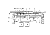
- FIG. 2 is an enlarged vertical sectional view of the substrate mounting table 15 of FIG. 2 is connected to an electrostatic chuck 61 made of aluminum nitride, a cooling jacket 62 made of aluminum disposed below the electrostatic chuck 61, and a lower side of the cooling jacket 62.
- a bracket 63 that forms a lift space for a wafer lifter driven by the lift cylinder 19 and a focus ring 64 disposed on the upper side of the electrostatic chuck 61 are configured.
- the electrostatic chuck 61 has an upper disk part 61a in which an electrode 71 for electrostatic adsorption is built, and a lower disk part having a larger diameter than the upper disk part 61a and in which a heater 72 is built in. 61b.
- the electrostatic chuck 61 is integrally formed of an upper disk part 61a and a lower disk part 61b.
- the substrate mounting table 15 in FIG. 2 includes an upper annular cover 65 for heat insulation that surrounds at least a part of the cooling jacket 62 and the lower disk portion 61b, and a lower side for heat insulation that surrounds the outer side of the bracket 63 in the radial direction.
- the cooling jacket 62 is sandwiched between the upper annular cover 65 and the lower annular cover 66.
- the electrode 71 for electrostatic attraction is connected to the power source 36 for electrostatic attraction, and the heater 72 for heating is connected to the power source 53 for heater of the temperature adjustment system 50.
- the upper disk portion 61a is formed in substantially the same planar shape and the same size as the substrate K placed on the upper surface.
- the heater 72 extends in a range of a diameter larger than the diameter of the substrate K in the lower disk portion 61b.
- the cooling jacket 62 includes an upper jacket main body 62a and a lower bottom 62b.
- the jacket main body 62 a is coupled to the lower surface of the electrostatic chuck 61 by a plurality of bolts 73.
- the bottom 62b is fitted into the lower recess of the jacket main body 62a, and is fixed to the jacket main body 62a by welding or the like.
- a coolant channel 74 for cooling is formed by the groove on the lower surface of the jacket main body 62a and the upper surface of the bottom 62b.
- the plurality of bolts 73 are arranged on one circumference centered on the mounting table axis O1.
- the refrigerant flow path 74 is formed in a spiral shape in a plan view, for example, and the refrigerant (Galden (registered trademark)) supplied from the chiller unit 51 flows through the connection port provided on the lower surface of the cooling jacket 62. By circulating through the path 74, the refrigerant that has taken away the heat of the wafer is returned to the chiller unit 51. In the chiller unit 51, the refrigerant is cooled and returned to the refrigerant flow path 74 again.
- heat removal means that the heat of the wafer is released outside through the surface of the bottom 62b of the cooling jacket 61.
- the heat of the wafer is released outside through the refrigerant, and a part of the heat of the wafer is radiated from the surface of the bottom 62b of the cooling jacket 61. This lowers the temperature of the wafer itself.
- the space surrounded by the bottom 62b of the cooling jacket 62 and the mounting table support member 69 is at atmospheric pressure.
- the refrigerant that has become hot due to the heat of the wafer is cooled in the chiller unit 51.
- An outward flange portion 62c is integrally formed at the lower end portion of the outer peripheral end in the radial direction of the jacket main body 62a.
- the flange portion 62c is composed of a ceramic upper annular cover 65 and a lower annular cover 66 for heat insulation. And are sandwiched from above and below.
- An annular notch 65a is formed at the upper end portion of the upper annular cover 65, and an inward flange portion 68a formed in the outer case 68 is engaged with the notch 65a.
- the upper end surface of the lower annular cover 66 abuts on the lower surface of the flange portion 62 c via the O-ring 75, and the lower end surface of the lower annular cover 66 abuts on the upper surface of the mounting table support member 69 via the O-ring 76.
- the upper annular cover 65 and the lower annular cover 66 are tightened from above and below by screwing bolts 77 inserted into the bolt insertion holes at the outer peripheral end of the outer case 68 into the female screw holes of the mounting table support member 69. .
- the focus ring 64 covers the upper surface of the lower disk part 61b outside the electrostatic disk 61 in the radial direction of the upper disk part 61a.
- the substrate K placed on the upper end chuck surface of the upper disk portion 61 a is located at substantially the same height as the upper surface of the focus ring 64.
- a minute gap 80 is formed between the upper surface of the jacket body 62a of the cooling jacket 62 and the lower surface of the electrostatic chuck 61 by increasing the surface roughness of the upper surface of the jacket body 62a.
- an O-ring 81 or an annular metal seal is disposed on the inner side of the circumference constituted by a plurality of bolts 73 for fixing the electrostatic chuck. It is configured in a sealed circular shape in plan view.
- a gas passage network 83 communicating with the central gas passage 82 of the shaft core O1 portion is formed on the upper surface of the jacket main body 62a.
- the central gas passage 82 communicates with a joint 85 screwed to the bracket 63 via a gas passage 84 formed in the bottom portion 62b.
- the joint 85 communicates with the vacuum pump 54 and the helium gas supply unit 52 of the temperature adjustment system 50 through a gas pipe 86 also serving as a suction pipe and a switching valve 87 so as to be switched.
- the helium gas supply unit 52 communicates with the upper surface (chuck surface) of the upper disk portion 61a through a joint 98 screwed to the bracket 63 and a gas passage, and can supply He gas to the back surface of the substrate K. It is configured as follows.
- FIG. 3 is a plan view of the cooling jacket 62 of FIG.
- a gas passage network 83 formed in a circular minute gap 80 surrounded by an O-ring 81 includes an outer annular passage 83a, an inner annular passage 83b, and both annular passages 83a and 83b.
- He gas supplied from the central gas passage 82 is evenly distributed over the entire circular minute gap 80. It is comprised so that it can supply to.
- the cooling jacket 62 is provided with a plurality of holes through which wiring for each power source is passed. Specifically, high-frequency power is applied to holes 90 and 96 through which wiring for electrostatic chuck power is passed, holes 93 and 94 through which wiring for heater power is passed, holes 89 and 97 for temperature monitor sensors, and electrodes on the mounting table. A hole 92 through which a wiring for applying a high frequency power is passed is provided. Further, lifter holes 88, 91, and 95 for lifting the back surface of the substrate K are provided.
- FIG. 4 is an explanatory view of the operation when the minute gap 80 is in a vacuum state at the time of temperature rise or standby
- FIG. 5 is when the minute gap 80 is in a He gas filling state during the process of placing the substrate K.
- FIGS. 4 and 5 are action explanatory views showing changes in the state in the minute gap 80, the solid line arrows show the heat transfer state, the white arrows show the He gas movement state, A broken arrow indicates a heat insulation state.
- the minute gap 80 is actually a thickness of several ⁇ m to several tens of ⁇ m, but is expressed in a greatly exaggerated state. As shown in FIG.
- the minute gap 80 is connected to the vacuum pump 54, and the He gas in the minute gap 80 is sucked to make the minute gap 80 in a vacuum state. Therefore, the minute gap 80 serves as a heat insulating layer, and it is possible to prevent the heat from the heater 72 from passing to the cooling jacket 62 side.
- the elevating cylinder 19 of FIG. 1 is lowered to place the substrate (wafer) K on the substrate mounting table 15 and attracted and held by the electrostatic chuck 61.
- the inside of the chamber 11 is heated to 120 ° C., for example, and the substrate K is heated to 200 ° C. by the heater 72 of the electrostatic chuck 61.
- SF 6 gas, SiF 4 gas, O 2 gas, inert gas, and the like supplied from the gas supply apparatus 20 into the upper chamber 12 by supplying high-frequency power to the coil 31 from the high-frequency power supply 32. Is turned into plasma.
- a high frequency voltage is also applied to the electrostatic chuck 61 from the high frequency power source 35.
- a potential difference is generated between the electrostatic chuck 61 and the plasma in the chamber 11, and ions in the plasma move toward the electrostatic chuck 61 due to the potential difference and collide with the surface of the substrate K. Etching is performed on the surface of the substrate K.
- SF 6 gas SiF 4 gas, O 2 gas, or the like is used in the plasma generation.
- a gas such as N 2 may be used depending on the object to be etched.
- the minute gap 80 is vacuumed because He gas is sucked by the vacuum pump 54. It is in a state.
- the minute gap 80 serves as a heat insulating layer, prevents heat from the heater 72 from passing to the cooling jacket 62 side, and prevents the heat from passing upward by the focus ring 64.
- the upper annular cover 65 prevents the heat from escaping outward. Thereby, the heat from the heater 72 can be collected in the central upper disk part 61. That is, the heat of the heater 62 can be efficiently collected in the upper disk portion 61. Therefore, efficient temperature rise can be achieved, power consumption of the heater 72 can be reduced, and energy saving can be achieved.
- the minute gap 80 is in a He gas filling state.
- the amount of heat generated by the substrate K is large, and it tends to be higher than a predetermined temperature of 200 ° C.
- the minute gap 80 is filled with He gas having a good heat transfer property, the heat of the substrate K can quickly pass through the minute gap 80 and reach (release) the cooling jacket 62. Therefore, the heat of the substrate K can be quickly removed to cool the substrate K. That is, it is possible to efficiently remove the heat from the substrate K.
- the back surface of the substrate K is filled with He gas having good heat transfer properties, the temperature distribution on the surface of the substrate K can be made uniform. Therefore, it is possible to suppress variations in the etching shape and etching rate due to variations in the temperature distribution on the surface of the substrate K.
- the electrostatic chuck 61 and the cooling jacket 62 shown in FIG. 2 are made of a ceramic focus ring 64 and a ceramic that have high heat insulating properties over the entire upper surface excluding the placement region of the substrate K and the entire outer region in the radial direction of the cooling jacket 62.
- the upper and lower annular covers 65 and 66 are covered. Examples of these ceramic materials include aluminum oxide (alumina), yttria, and quartz.
- the cooling action by the cooling jacket 62 can be concentrated on the electrostatic chuck 61, and the temperature rise of the substrate K can be suppressed. It becomes.
- the lower surface of the cooling jacket 62 is in an atmospheric pressure state, but is surrounded by the lower annular cover 66 and the mounting table support member 69, and therefore, the amount of heat released from the cooling jacket 62 by convection is very small.
- FIG. 6 is a graph showing temporal changes in the electrostatic chuck temperature, the heat removal amount, and the He gas pressure in the non-processed state.
- FIG. 6 shows a time lapse in a non-processing state from the heating step T1 of the electrostatic chuck 61 to the cooling step T3 by the cooling jacket 62 through the constant temperature step T2 in which the electrostatic chuck 61 is maintained at a temperature of 200 ° C.
- the change in the electrostatic chuck temperature (° C.) is indicated by a solid curve S1
- the change in the He gas pressure (Pa) in the minute gap 80 is indicated by a dashed curve S2
- the change in the heat removal amount (W) S3 is represented by two. This is indicated by a dashed line curve S3.
- the He gas pressure (Pa) in the minute gap 80 is reduced to about 100 Pa, which is close to absolute vacuum.
- the minute gap 80 functions as a heat insulating layer, and the heat removal to the cooling jacket 62 can be suppressed as much as possible as shown in FIG.
- the heating time for the temperature of the electrostatic chuck 61 to reach 200 ° C. from 50 ° C. in the heating step T1 was about 17 minutes.
- the amount of heat removal (W) could be reduced by reducing the He gas pressure (Pa).
- the heater 72 in FIG. 2 is stopped, and the minute gap 80 is in a state of being filled with He gas at approximately 1000 Pa as shown in FIG. Thereby, the heat removal amount (W) to the cooling jacket 62 increases to the maximum P1.
- FIG. 7 is a graph showing the temporal change of the electrostatic chuck temperature and the heater load factor in the non-processed state.
- FIG. 7 shows a time lapse in a non-process state following the cooling step T3 by the cooling jacket 62 through the constant temperature step T2 in which the electrostatic chuck 61 is maintained at a temperature of 200 ° C. from the heating step T1, as in FIG.
- the change of the electrostatic chuck temperature (° C.) and the load factor (%) of the heater 72 is shown.
- the change in the electrostatic chuck temperature is indicated by a solid curve S1
- the change in the load factor (%) of the heater 72 is indicated by a solid curve S4. It can be understood that when the current upper limit of the heater is 1 kW, the maximum load factor of the temperature raising step T1 is suppressed to about 40%, and the capacity of the heater 72 can be reduced.
- the heater 72 is arranged in a larger area than the substrate K, so that the temperature distribution on the electrostatic chuck 61 is uniform from the center of the substrate K to the outer peripheral edge. Distribution.
- the minute gap 80 that can be switched between the He gas filling state and the vacuum state is formed at the joint between the lower surface of the electrostatic chuck 61 and the upper surface of the cooling jacket 62, the non-processed state shown in FIG.
- the minute gap 80 is made into a vacuum state, thereby preventing the heat of the electrostatic chuck 61 from escaping to the cooling jacket 62 below, and efficient initial temperature rise and A standby state at a predetermined temperature can be maintained.
- the minute gap 80 is filled with the He gas, so that the heat of the high-temperature substrate K is quickly released to the cooling jacket 62 through the He gas having a good heat transfer property. It is possible to remove heat.
- the plasma processing apparatus 1 since the plasma processing apparatus 1 includes the substrate mounting table 15 that facilitates temperature control of the substrate K and the electrostatic chuck 61, temperature management during the processing of the substrate K can be easily performed. Can do. Therefore, it is possible to avoid non-uniform processing results where reproducibility due to unstable or non-uniform wafer temperatures cannot be obtained.
- the lower surface of the electrostatic chuck and the cooling jacket are directly joined, but the present invention is not limited to this.
- a heat insulating plate having a low thermal conductivity for example, a quartz plate
- a small gap may be formed between the upper surface and the upper surface. Even in this case, the same effect as the present embodiment can be obtained.
- the outer peripheral end portion in the radial direction of the minute gap 80 is sealed with an O-ring, but the present invention is not limited to this.
- the outer peripheral end portion of the minute gap 80 in the radial direction may be sealed with a heat-resistant metal seal. Even in this case, the same effect as the present embodiment can be obtained.
- the upper annular cover 65 and the lower annular cover 66 are formed as separate bodies, but they may be configured so as to be integrally formed. Even in this case, the same effect as the present embodiment can be obtained.
- the etching process has been described.
- the present invention is not limited to this, and the present invention can also be used for a film forming process using a CVD method (chemical vapor deposition method) or the like. Reaction heat may also be generated in this film forming process, and is particularly useful when precise temperature control is required at a temperature of about 100 to 300 ° C., which is a low temperature region of the film forming process.
- CVD method chemical vapor deposition method
- Plasma processing apparatus 15 Substrate mounting base 50 Temperature control system 52 Helium gas supply part 54 Vacuum pump 61 Electrostatic chuck 61a Upper disk part 61b Lower disk part 62 Cooling jacket 62c Flange part 64 Focus ring 65 Upper ring cover 66 Lower ring Cover 71 Electrode for electrostatic adsorption 72 Heater 74 Refrigerant flow path 80 Minute gap 81 O-ring
Abstract
チャンバ(11)内の温度等の外部要因の影響を軽減できる基板載置台(15)を提供する。プラズマ処理装置(1)におけるチャンバ(11)内に配置された基板載置台(15)は、静電チャック(61)と冷却ジャケット(62)を備えており、静電チャック(61)は、静電吸着用電極(71)を内蔵する上側円盤部(61a)と、上側円盤部(61a)より大きい径を有し、かつヒータ(72)を内蔵する下側円盤部(61b)とから構成されている。上側円盤部(61a)の径方向外方に配置されて下側円盤部(61b)の上面を覆うフォーフォーカスリング(64)と、冷却ジャケット(62)の少なくとも一部及び下側円盤部(61b)を囲む断熱用の上側環状カバー(65)と、上側環状カバー(65)とで冷却ジャケット(62)を挟持する断熱用の下側環状カバー(66)とが、セラミック製である。
Description
本発明は、チャンバ内でプラズマエッチング処理等が施される基板、たとえば半導体用のウェハを静電吸着状態で載置する基板載置台及びこれを備えたプラズマ処理装置及びプラズマ処理方法に関する。
従来、チャンバ内に配置された基板載置台に、被処理ワークとして半導体用の基板を載置し、チャンバ内に所定のガスを供給してプラズマ化させ、プラズマ化した処理ガスによって、基板にエッチング処理を施すプラズマ処理装置が知られている。また、プラズマ処理に適した基板載置台として、静電吸着用の電極及び基板加熱用のヒータを内蔵する静電チャックと、この静電チャックの下側に配置された冷却ジャケットとを備えたものが開発されている(特許文献1及び2)。この種の基板載置台は、静電吸着用の電極に電圧を印加することにより、電極表面から静電チャックの上端チャック面にかけての誘電層で誘電分極を起こし、基板との間で発生する静電力により、基板をチャック面に吸着保持する。そして処理中は、ヒータ及び冷却ジャケットによる温度制御により、基板を所定温度に保った状態として、基板にエッチング処理等が施される。
しかしながら、ヒータ及び冷却ジャケットによる静電チャック及び基板の温度制御に関し、基板載置台の周囲環境、たとえばチャンバ内温度の影響により、静電チャック及び基板の適切な温度制御が困難になるという問題がある。たとえば、基板を載置していない非処理状態での初期昇温時や所定温度での待機時には、加熱される静電チャックの熱は下側の冷却ジャケットを介して多量に外部に逃げる。このために、大きなヒータ容量が要求され、無駄な電力消費の要因となる。一方、基板を載置してエッチング処理等を行う処理中には、温度上昇した基板から静電チャックに多くの熱が連続的に伝達されるので、大きな抜熱量が要求される。具体的に説明すると、非処理状態における静電チャックの昇温工程並びに所定温度、たとえば200℃での待機時(一定温度工程)では、ヒータによる熱が外部に逃げないようにして、静電チャックを効率良く昇温させ、または静電チャックを一定温度に保つ必要がある。一方、基板の処理中、たとえプラズマエッチング処理中には、基板が必要以上に高温にならないように、基板の熱を効率良く静電チャックを通じて抜熱する必要がある。
本発明の目的は、以上の実情に鑑みなされたものであって、チャンバ内温度等の外部要因が静電チャック及び冷却ジャケットに及ぼす影響を軽減し、基板及び静電チャックの温度制御を容易にすることが可能な基板載置台及びこれを備えたプラズマ処理装置及びプラズマ処理方法の提供をその目的とする。
上記目的を達成するための本発明は、
被処理用の基板を静電吸着する基板載置台であって、
前記基板を静電吸着する電極を内蔵する上側円盤部と、該上側円盤部の下側に、前記上側円盤部より大きな径を有するとともにヒータを内蔵する下側円盤部とからなる静電チャックと、
前記下側円盤部の下側に配置され、前記静電チャックを冷却する冷却ジャケットと、
前記上側円盤部の径方向外方に配置され、前記下側円盤部の上面を覆うフォーカスリングと、
前記冷却ジャケットの少なくとも一部及び前記下側円盤部を囲む断熱用の上側環状カバーと、
前記上側環状カバーとで前記冷却ジャケットを挟持する断熱用の下側環状カバーとを備え、
前記フォーカスリング、前記上側環状カバー及び前記下側環状カバーは、セラミック製である基板載置台に係る。
この基板載置台によれば、静電チャック及び冷却ジャケットの上面及び径方向の外方を囲むフォーカスリング、断熱用の上下の環状カバーを、セラミック製としているので、静電チャック及び冷却ジャケットに対する外部影響を軽減でき、静電チャック及び基板に対して効率の良い温度制御が可能となる。
また、前記基板載置台において、前記ヒータの配置領域は、前記基板の径よりも大きな径を有していることが好ましい。
この基板載置台によれば、ヒータの配置領域を、基板の径よりも大きな径に設定されているので、静電チャック上の温度分布を、基板の中心部から外周端部まで均一な分布とすることができる。
また、前記基板載置台において、
前記冷却ジャケットの径方向外周面に外向きのフランジ部が一体に形成され、
前記フランジ部は、前記上側環状カバーと前記下側環状カバーとにより上下から挟持されていることが好ましい。
前記冷却ジャケットの径方向外周面に外向きのフランジ部が一体に形成され、
前記フランジ部は、前記上側環状カバーと前記下側環状カバーとにより上下から挟持されていることが好ましい。
この基板載置台によれば、上下のセラミック製の環状カバーで冷却ジャケットの外向きフランジを挟持するので、上下の環状カバーを、静電チャック及び冷却ジャケットに対する断熱機能に加え、冷却ジャケットの保持部材としても利用できる。
さらに、前記基板載置台において、
前記静電チャックと前記冷却ジャケットとの間には、前記ヒータの配置領域の全域に延在するとともに外部から密封された微小隙間が形成され、
前記微小隙間は、ヘリウムガス供給部と真空ポンプとに切り換え自在に接続されることにより、ヘリウムガス充填状態と真空状態との間で変更自在となるように構成されることが好ましい。
前記静電チャックと前記冷却ジャケットとの間には、前記ヒータの配置領域の全域に延在するとともに外部から密封された微小隙間が形成され、
前記微小隙間は、ヘリウムガス供給部と真空ポンプとに切り換え自在に接続されることにより、ヘリウムガス充填状態と真空状態との間で変更自在となるように構成されることが好ましい。
この基板載置台によれば、非処理状態における初期昇温時、一定温度での待機時には、微小隙間を真空状態とする。したがって、静電チャックの熱が下方の冷却ジャケットへ逃げるのを遮断し、効率的な初期昇温及び所定温度での待機状態を維持することができる。一方、プラズマ処理中は、微小隙間をヘリウムガス充填状態とすることにより、高温の基板の熱を、熱伝達性の良いヘリウムガスを介して速やかに冷却ジャケットへと逃がし、効率的な抜熱を行うことができる。
またさらに、前記基板載置台において、前記静電チャックは、窒化アルミニウム製であることが好ましい。
この基板載置台によれば、静電チャックとして、高熱伝導性の窒化アルミニウムを用いるので、酸化アルミニウムよりも良好な温度分布が期待でき静電チャックの熱応力による割れを防止することができる。
また、本発明は、前記基板載置台がチャンバ内に内蔵されているプラズマ処理装置を提供する。
このプラズマ処理装置によれば、基板及び静電チャックの温度制御を容易とする基板載置台を備えているので、基板の処理中での温度管理を容易に実施することができる。したがって、不安定又は不均一なウェハ温度に起因する再現性が得られない不均一な処理結果を回避することが可能となる。
さらに本発明は、基板処理方法も提供するものであり、前記基板載置台と前記冷却ジャケットとの間に微小隙間を有する基板載置台において、基板非処理状態における初期昇温時又は待機時には、前記微小隙間を真空状態とし、基板処理中は、前記微小隙間をヘリウムガス充填状態とする。
この方法によると、非処理中は、静電チャックの熱が下方の冷却ジャケットへ逃げるのを遮断し、効率的な初期昇温及び所定温度での待機状態を維持することができる。一方、基板処理中は、高温の基板の熱を、熱伝達性の良いヘリウムガスを介して速やかに冷却ジャケットへと逃がし、効率的な抜熱を行うことができる。
以上のように、本発明に係る基板載置台又は処理方法によれば、チャンバ内温度等の外部要因が静電チャック及び冷却ジャケットに及ぼす影響を軽減し、基板及び静電チャックの温度制御を容易にすることができる。また、本発明に係るプラズマ処理装置によれば、不安定又は不均一なウェハ温度に起因する再現性が得られない不均一な処理結果を回避することが可能となる。
以下、本発明に係る実施形態について図面を参照して説明する。
実施形態.
図1は本発明の一実施形態に係るプラズマ処理装置1の概略的な構成を示す縦断面図である。図1のプラズマ処理装置1は、閉塞空間を有するチャンバ11と、このチャンバ11内に昇降シリンダ(図示せず)により昇降自在に配設され、ウェハ等の被処理用の基板Kが載置される基板載置台15と、該基板載置台15内にあって、ウェハリフタを昇降させる昇降シリンダ19と、チャンバ11内にエッチングガス、保護膜形成ガス及び不活性ガスを供給するガス供給装置20と、チャンバ11内に供給されたエッチングガス、保護膜形成ガス及び不活性ガスをプラズマ化するプラズマ生成装置30と、チャンバ11内の圧力を減圧する排気装置40と、基板載置台15にプラズマ処理用の高周波電力を供給する高周波電源35と、基板載置台15に静電吸着用の電圧を印加する静電吸着用電源36とを備えて構成される。さらに、基板載置台15及び基板Kの温度を調整するための各種装置からなる温度調整システム50を備える。
図1は本発明の一実施形態に係るプラズマ処理装置1の概略的な構成を示す縦断面図である。図1のプラズマ処理装置1は、閉塞空間を有するチャンバ11と、このチャンバ11内に昇降シリンダ(図示せず)により昇降自在に配設され、ウェハ等の被処理用の基板Kが載置される基板載置台15と、該基板載置台15内にあって、ウェハリフタを昇降させる昇降シリンダ19と、チャンバ11内にエッチングガス、保護膜形成ガス及び不活性ガスを供給するガス供給装置20と、チャンバ11内に供給されたエッチングガス、保護膜形成ガス及び不活性ガスをプラズマ化するプラズマ生成装置30と、チャンバ11内の圧力を減圧する排気装置40と、基板載置台15にプラズマ処理用の高周波電力を供給する高周波電源35と、基板載置台15に静電吸着用の電圧を印加する静電吸着用電源36とを備えて構成される。さらに、基板載置台15及び基板Kの温度を調整するための各種装置からなる温度調整システム50を備える。
図1に示すように、チャンバ11は、相互に連通した内部空間を有する上チャンバ12及び下チャンバ13から構成され、上チャンバ12は、下チャンバ13よりもその内径が小径となるように形成されている。上チャンバ12の天板の内部には、上チャンバヒータ(図示せず)が設けられる一方、下チャンバの側壁の内部には、下チャンバヒータがブロックヒータとして備えられている。このブロックヒータは、例えば、アルミニウムからなるブロック体に発熱体を組み入れることにより形成される。
ガス供給装置20は、エッチングガスとして、SF6ガスを供給するSF6ガス供給部21と、保護膜形成ガスとして、SiF4ガス及びO2ガスをそれぞれ供給するSiF4ガス供給部22及びO2ガス供給部23と、不活性ガスとして、例えば、Arガスなどを供給する不活性ガス供給部24とを備える。ガス用の供給管25は、一端が上チャンバ12の上面に接続し、他端が分岐してSF6ガス供給部21、SiF4ガス供給部22、O2ガス供給部23及び不活性ガス供給部24にそれぞれ接続している。SF6ガス供給部21、SiF4ガス供給部22、O2ガス供給部23及び不活性ガス供給部24から供給管25を介して、チャンバ11内にSF6ガス、SiF4ガス、O2ガス及び不活性ガスを供給する。なお、本実施形態では、上述したガスを用いたが、エッチングする対象によっては、例えばHBr、Cl2、SF6、O2、Ar、N2などのガスを用いてもよい。
プラズマ生成装置30は、誘導結合プラズマ(ICP)を生成する装置であって、上チャンバ12に配設された螺旋状(環状)のコイル31と、このコイル31に高周波電力を供給する高周波電源32とから構成されている。高周波電源32によってコイル31に高周波電力を供給することで、上チャンバ12内に供給されたSF6ガス、SiF4ガス、O2ガス及び不活性ガスをプラズマ化する。
基板載置台15に接続される高周波電源35は、基板載置台15の静電チャック61に高周波電力を供給することで、静電チャック61とプラズマとの間にバイアス電位を与え、SF6ガス、SiF4ガス、O2ガス及び不活性ガスのプラズマ化により生成されたイオンを、基板載置台15上に載置された基板Kに入射させる。なお、本実施形態では、プラズマ化する際において、SF6ガス、SiF4ガス、O2ガス等を用いたが、エッチングする対象によっては、例えばHBr、Cl2、SF6、O2、Ar、N2などのガスを用いてもよい。
排気装置40は、チャンバ11内の気体を吸引し、排気する真空ポンプ41と、排気管42とから構成されており、排気管42は、一端が真空ポンプ41に接続し、他端が下チャンバ13の側面に接続している。この排気管42を介して、真空ポンプ41がチャンバ11内の気体を吸引し、チャンバ11内部を真空状態とする。
温度調整システム50は、基板載置台15内の加熱用ヒータ72に電力を供給するヒータ用電源53と、基板載置台15に冷却用の冷媒を供給するチラーユニット51と、熱伝達性の良いヘリウムガス(以下、Heガスという。)を基板載置台15に供給するヘリウムガス供給部52と、基板載置台15内に断熱用の真空層(後述する図2の微小隙間80)を形成するための真空ポンプ54とを備えて構成される。この真空ポンプ54は、前述のチャンバ用の真空ポンプ41を流用することもできる。
図2は図1の基板載置台15の縦断面拡大図である。図2の基板載置台15は、窒化アルミニウム製の静電チャック61と、この静電チャック61の下側に配置されたアルミニウム製の冷却ジャケット62と、この冷却ジャケット62の下側に連結され、昇降シリンダ19が駆動するウェハリフタの昇降空間を形成するブラケット63と、静電チャック61の上側に配置されたフォーカスリング64とを備えて構成される。また、静電チャック61は、静電吸着用の電極71を内蔵する上側円盤部61aと、この上側円盤部61aよりも大きな径を有し、かつ、加熱用ヒータ72を内蔵する下側円盤部61bとから構成されている。ここで、静電チャック61は、上側円盤部61aと、下側円盤部61bとから一体形成されている。
さらに、図2の基板載置台15は、冷却ジャケット62の少なくとも一部及び下側円盤部61bを囲む断熱用の上側環状カバー65と、ブラケット63の径方向の外方を囲む断熱用の下側環状カバー66と、上側環状カバー65及び下側環状カバー66の径方向の外周を囲む外郭ケース68と、この外郭ケース68の下面に連結され、基板載置台15の全体を支持する載置台支持部材69とを備えて構成される。ここで、上側環状カバー65と下側環状カバー66とで冷却ジャケット62を挟持する。
静電吸着用の電極71は静電吸着用電源36に接続され、加熱用ヒータ72は、温度調整システム50のヒータ用電源53に接続されている。上側円盤部61aは、上面に載置される基板Kと略同じ平面形状及び同じ広さに形成されている。静電吸着用電極71に、静電吸着用電源36による電圧を印加すると、静電誘導により、基板Kが上側円盤部61aの上端チャック面に吸着保持される。加熱用ヒータ72は、下側円盤部61b内で、基板Kの径よりも大きな径の範囲に延在している。
冷却ジャケット62は、上側のジャケット本体62aと下側の底部62bとから構成されている。ジャケット本体62aは、複数本のボルト73により静電チャック61の下面に結合されている。底部62bは、ジャケット本体62aの下側凹部に嵌合し、溶接等によりジャケット本体62aに固着されている。ジャケット本体62aの下面の溝と底部62bの上面とで冷却用の冷媒流路74を形成している。複数本のボルト73は、載置台軸心O1を中心とする一つの円周上に配列されている。冷媒流路74は、たとえば平面視で螺旋状に形成されており、チラーユニット51から供給される冷媒(ガルデン(登録商標))が、冷却ジャケット62の下面に設けられた接続口を通じて、冷媒流路74を循環することにより、ウェハの熱を奪った冷媒をチラーユニット51内へと戻るように構成されている。チラーユニット51では、冷媒は冷却され、再度冷媒流路74に戻される。ここで、抜熱とは、ウェハの熱を冷媒および冷却ジャケット61の底部62b表面を介して外に逃がすことをいう。さらに、ウェハの熱のほとんどは冷媒を介して外に逃がされ、ウェハの熱の一部は冷却ジャケット61の底部62b表面から放熱される。これにより、ウェハ自身の温度を下げる。なお、冷却ジャケット62の底部62bと載置台支持部材69で囲まれた空間は大気圧状態である。また、ウェハの熱を奪って高温となった冷媒はチラーユニット51内で冷却される。
ジャケット本体62aの径方向外周端の下端部には、外向きのフランジ部62cが一体に形成されており、このフランジ部62cは、断熱用のセラミック製の上側環状カバー65と下側環状カバー66とにより、上下から挟持されている。
上側環状カバー65の上端部には、環状の切り欠き65aが形成されており、この切り欠き65aには外郭ケース68に形成された内向きフランジ部68aが係合している。下側環状カバー66の上端面はOリング75を介してフランジ部62cの下面に当接し、下側環状カバー66の下端面はOリング76を介して載置台支持部材69の上面に当接している。外郭ケース68の外周端部のボルト挿通孔に挿通したボルト77を、載置台支持部材69のめねじ孔に螺着することにより、上側環状カバー65及び下側環状カバー66を上下から締め付けている。この構成により、上下の環状カバー65、66及び冷却ジャケット62のフランジ部62cを上下から固定しており、かつ、下側環状カバー66の上下の両Oリング75、76を圧縮することにより、下チャンバ13を密封している。なお、冷却ジャケット62と載置台支持部材69で囲まれた空間は大気圧状態である。
フォーカスリング64は、静電チャック61の上側円盤部61a径方向の外方において、下側円盤部61bの上面を覆っている。上側円盤部61aの上端チャック面に載置される基板Kは、フォーカスリング64の上面と略同一高さに位置している。
冷却ジャケット62のジャケット本体62aの上面と静電チャック61の下面との間には、ジャケット本体62aの上面の面粗度を大きくすることにより、微小隙間80が形成されている。ジャケット本体62aの上面には、静電チャック固定用の複数のボルト73で構成する円周の内側に、Oリング81もしくは環状メタルシールが配置されており、このOリング81により、微小隙間80を平面視で密封状態の円形に構成している。また、ジャケット本体62aの上面には、軸芯O1部分の中央ガス通路82に連通するガス通路網83が形成されている。中央ガス通路82は、底部62bに形成されたガス通路84を介して、ブラケット63に螺着された継手85に連通している。
継手85は、吸引管を兼ねるガス管86及び切り換えバルブ87を介して、前述の温度調整システム50の真空ポンプ54及びヘリウムガス供給部52に切り換え自在に連通している。
また、ヘリウムガス供給部52は、ブラケット63に螺着された継手98及びガス通路を介して上側円盤部61aの上面(チャック面)に連通しており、基板Kの裏面にHeガスを供給できるように構成されている。
図3は図2の冷却ジャケット62の平面図である。図3に示すように、Oリング81で囲まれた円形の微小隙間80に形成されたガス通路網83は、外側環状通路83aと、内側環状通路83bと、両環状通路83a、83bを相互に連通するY字形通路83cと、内側環状通路83bを中央ガス通路82に連通する通路83d等を有しており、中央ガス通路82から供給されるHeガスを、円形の微小隙間80の全体に均等に供給できるように構成されている。
また、図3に示すように、冷却ジャケット62には各電源用の配線を通す穴が複数設けられている。具体的には、静電チャック電源用の配線を通す穴90,96、ヒータ電源用の配線を通す穴93,94、温度モニタセンサ用の穴89,97、および載置台の電極に高周波電力を印加する高周波電源用の配線を通す穴92が設けられている。さらに、基板Kの裏面を持ち上げるリフタ用の穴88,91,95が設けられている。
図4は昇温時または待機時に微小隙間80を真空状態にしている時の作用説明図であり、図5は基板Kを載置した処理時において微小隙間80をHeガス充填状態にしている時の作用説明図である。ここで、図4及び図5は、微小隙間80内の状態の変化を示す作用説明図であり、実線の矢印は熱の伝達状態を示し、白抜きの矢印はHeガスの移動状態を示し、破線の矢印は断熱状態を示している。なお、図中、微小隙間80は、実際には数μm~数十μmの厚みであるが、大きく誇張した状態で表現している。図4のように微小隙間80を真空ポンプ54に接続し、微小隙間80内のHeガスを吸引することにより、微小隙間80内を真空状態とすることができる。したがって、微小隙間80は断熱層の役割を担い、ヒータ72からの熱が冷却ジャケット62側へ抜けるのを阻止することが可能となる。
一方、図5のように、微小隙間80をヘリウムガス供給部52に接続すると、微小隙間80には熱伝達性の良いHeガスが供給されるとともに圧力も上昇し、Heガス充填状態となる。ここで、Heガスは、静電チャック61の裏面の熱を冷却ジャッケット62表面に熱移動させる。これにより、冷却ジャケット62の熱は冷媒を通して外部に放出される。このように、処理中に発熱する基板Kの熱は、微小隙間80を速やかに通過して冷却ジャケット62に到達することができるので、基板Kの熱を速やかに抜熱することが可能となる。
本実施形態の基板載置台15及びプラズマ処理装置1の作用効果を説明する。
プラズマエッチング処理の前工程において、図1の昇降シリンダ19を下降させ基板載置台15に基板(ウェハ)Kを載せ、静電チャック61により吸着保持する。この時、チャンバ11内はたとえば120℃に加熱され、基板Kは静電チャック61のヒータ72により200℃に加熱される。
プラズマ生成装置30において、高周波電源32によってコイル31に高周波電力を供給することにより、ガス供給装置20から上チャンバ12内に供給されたSF6ガス、SiF4ガス、O2ガス及び不活性ガス等をプラズマ化する。一方、静電チャック61にも高周波電源35から高周波電圧を印加する。これにより、静電チャック61とチャンバ11内のプラズマとの間で電位差が生じ、この電位差により、プラズマ中のイオンが静電チャック61に向けて移動し、基板Kの表面に衝突することで、基板Kの表面にエッチング処理が施される。なお、本実施形態では、プラズマ化する際において、SF6ガス、SiF4ガス、O2ガス等を用いたが、エッチングする対象によっては、例えばHBr、Cl2、SF6、O2、Ar、N2などのガスを用いてもよい。
図4の非処理状態において、ヒータ72による基板載置台15の昇温時または200℃を維持した状態の待機時には、微小隙間80は、Heガスを真空ポンプ54で吸引していることにより、真空状態となっている。これにより、微小隙間80は断熱層の役割を担い、ヒータ72からの熱が冷却ジャケット62側へ抜けるのを阻止し、かつ、熱が上方に抜けるのをフォーカスリング64により阻止する。さらに、熱が外方に抜けるのを上側環状カバー65により阻止する。これにより、ヒータ72からの熱を中央の上側円盤部61へと集めることができる。すなわち、ヒータ62の熱を効率良く上側円盤部61に集めることが可能となる。したがって、効率の良い昇温が達成でき、ヒータ72の消費電力を軽減でき、省エネを達成できる。
図5の処理状態において、微小隙間80はHeガス充填状態となっている。処理中は、基板Kの発熱量が大きく、所定の温度200℃より高くなろうとする。ところが、微小隙間80には、熱伝達性の良いHeガスが充填されているので、基板Kの熱は、微小隙間80を速やかに通過して冷却ジャケット62に到達する(逃がす)ことができる。したがって、基板Kの熱を速やかに抜熱し、基板Kを冷却することが可能となる。即ち、基板Kの効率の良い抜熱が可能となる。また、基板Kの裏面に熱伝達性の良いHeガスが充填されているので、基板Kの表面の温度分布を均一化することが可能となる。したがって、基板Kの表面の温度分布のバラツキによるエッチング形状やエッチング速度等のバラツキを抑制することが可能となる。
図2の静電チャック61及び冷却ジャケット62は、基板Kの載置領域を除く上面全域と、冷却ジャケット62の径方向の外方全域とが、断熱性の高いセラミック製のフォーカスリング64及びセラミック製の上下の環状カバー65、66により覆われている。これらのセラミックの材質として、例えば、酸化アルミニウム(アルミナ)、イットリア、石英が挙げられる。この構成により、冷却ジャケット62への熱放射や熱伝導による外乱の入熱を減少させることができチャンバ11内温度が基板載置台15の内部に影響を及ぼすことを阻止できる。したがって、効率良く基板載置台15内の温度調節を行うことが可能となる。たとえば、チャンバ11内の温度が120℃に対し、冷却ジャケット62を容易に70℃程度に維持することが可能となる。これにより、200℃の静電チャック62との間で大きな温度勾配を形成でき、冷却ジャケット62による冷却作用を静電チャック61に集中させることができ、基板Kの温度上昇を抑制することが可能となる。なお、冷却ジャケット62の下面は、大気圧状態であるが、下側環状カバー66及び載置台支持部材69とで囲まれているため、対流による冷却ジャケット62からの放熱量はごく僅かである。
図6は非処理状態における静電チャック温度、抜熱量及びHeガス圧力の時間的変化を示すグラフである。図6は、静電チャック61の加熱工程T1から、静電チャック61が温度200℃に維持される一定温度工程T2を経て、冷却ジャケット62による冷却工程T3へと続く非処理状態での時間経過において、静電チャック温度(℃)の変化を実線の曲線S1で示し、微小隙間80内のHeガス圧力(Pa)の変化を破線の曲線S2で示し、抜熱量(W)S3の変化を二点鎖線の曲線S3で示している。
加熱工程T1及び一定温度工程T2では、微小隙間80のHeガス圧力(Pa)は、絶対真空に近い100Pa程度まで低下させている。これにより、微小隙間80は断熱層として機能し、図4のように冷却ジャケット62への抜熱を極力抑制することができる。実際に試験を行った結果、加熱工程T1で静電チャック61の温度が50℃から200℃へと到達する昇温時間は約17分であった。この加熱工程T1ではHeガス圧力(Pa)を低下させることにより抜熱量(W)を削減することができた。
冷却工程T3では、図2のヒータ72を止め、図6のように、微小隙間80を略1000PaのHeガス充填状態としている。これにより、冷却ジャケット62への抜熱量(W)は最大P1まで上がる。
図7は非処理状態における静電チャック温度及びヒータ負荷率の時間的変化を示すグラフである。図7は、図6と同様、加熱工程T1から、静電チャック61が温度200℃に維持される一定温度工程T2を経て、冷却ジャケット62による冷却工程T3に続く非処理状態での時間経過において、静電チャック温度(℃)と、ヒータ72の負荷率(%)の変化を示している。静電チャック温度の変化を実線の曲線S1で示し、ヒータ72の負荷率(%)の変化を実線の曲線S4で示している。現状のヒータ上限が1kWのものにおいて、昇温工程T1の最大負荷率が40%程度に抑制されており、ヒータ72の小容量化が可能となることが理解できる。
本実施形態による効果を簡単に纏めると以下の通りとなる。
(1)図2において、静電チャック61及び冷却ジャケット62の上面及び径方向の外方を囲むフォーカスリング64、断熱用の上下の環状カバー65、66を、セラミックとしているので、静電チャック61及び冷却ジャケット62に対するジャケット11内の温度等の外部影響を軽減でき、静電チャック61及び基板Kに対して効率の良い温度制御が可能となる。
(2)図2において、ヒータ72の配置領域を、基板Kの径よりも大きな径に設定されているので、静電チャック61上の温度分布を、基板Kの中心部から外周端部まで均一な分布とすることができる。
(3)図4において、上下のセラミック製の環状カバー65、66で、冷却ジャケット62の外向きフランジ部62cを挟持しているので、上下の環状カバー65、66を、静電チャック61及び冷却ジャケット62に対する外部からの断熱機能に加え、冷却ジャケット62の保持部材としての役割も担っている。
(4)Heガス充填状態と真空状態とに切り換え自在な微小隙間80を、静電チャック61の下面と冷却ジャケット62の上面との接合部に形成しているので、図4に示す非処理状態における初期昇温時、一定温度での待機時には、微小隙間80を真空状態とすることにより、静電チャック61の熱が下方の冷却ジャケット62へ逃げるのを遮断し、効率的な初期昇温及び所定温度での待機状態を維持することができる。一方、プラズマ処理中は、微小隙間80をHeガス充填状態とすることにより、高温の基板Kの熱を、熱伝達性の良いHeガスを介して速やかに冷却ジャケット62へと逃がし、効率的な抜熱を行うことが可能となる。
(5)静電チャック61として、高熱伝導性の窒化アルミニウムを用いているので、酸化アルミニウムよりも良好な温度分布が期待でき静電チャック61の熱応力による割れを防止することができる。
(6)さらに、プラズマ処理装置1は、基板K及び静電チャック61の温度制御を容易とする基板載置台15を備えているので、基板Kの処理中での温度管理を容易に実施することができる。したがって、不安定又は不均一なウェハ温度に起因する再現性が得られない不均一な処理結果を回避することが可能となる。
なお、本実施形態では、静電チャックの下面と冷却ジャケットとを直接に接合しているが、本発明はこれに限定されない。例えば、冷却ジャケットと静電チャックとの間に熱伝導性の低い断熱板(たとえば石英板)を配置し、断熱板の上面と静電チャックの下面との間、断熱板の下面と冷却ジャケットの上面との間に、それぞれ微小隙間を形成するように構成されてもよい。この場合においても本実施形態と同様の効果を得ることができる。
また、本実施形態では、図2及び図3に示すように、微小隙間80の径方向の外周端部分をOリングでシールしているが、本発明はこれに限定されない。例えば、微小隙間80の径方向の外周端部分を熱に強いメタルシールでシールするように構成されてもよい。この場合においても本実施形態と同様の効果を得ることができる。また、本実施形態では、上側環状カバー65と下側環状カバー66とが別体で形成されたが、これらが一体で形成されるように構成されてもよい。この場合においても本実施形態と同様の効果を得ることができる。さらに、本実施形態では、エッチング処理について説明したが、本発明はこれに限定されず、CVD法(化学気相成長法)などを用いた成膜処理にも利用することが可能である。この成膜処理においても反応熱が生じることがあり、特に、成膜処理の低温領域である100~300℃程度の温度で、正確な温度制御が必要なときに有用である。
上述の実施形態は例示に過ぎず、この発明の範囲から逸脱することなく種々の変形が可能である。
1 プラズマ処理装置
15 基板載置台
50 温度調整システム
52 ヘリウムガス供給部
54 真空ポンプ
61 静電チャック
61a 上側円盤部
61b 下側円盤部
62 冷却ジャケット
62c フランジ部
64 フォーカスリング
65 上側環状カバー
66 下側環状カバー
71 静電吸着用電極
72 ヒータ
74 冷媒流路
80 微小隙間
81 Oリング
15 基板載置台
50 温度調整システム
52 ヘリウムガス供給部
54 真空ポンプ
61 静電チャック
61a 上側円盤部
61b 下側円盤部
62 冷却ジャケット
62c フランジ部
64 フォーカスリング
65 上側環状カバー
66 下側環状カバー
71 静電吸着用電極
72 ヒータ
74 冷媒流路
80 微小隙間
81 Oリング
Claims (7)
- 被処理用の基板を静電吸着する基板載置台であって、
前記基板を静電吸着する電極を内蔵する上側円盤部と、該上側円盤部の下側に、前記上側円盤部より大きな径を有するとともにヒータを内蔵する下側円盤部とからなる静電チャックと、
前記下側円盤部の下側に配置され、前記静電チャックを冷却する冷却ジャケットと、
前記上側円盤部の径方向外方に配置され、前記下側円盤部の上面を覆うフォーカスリングと、
前記冷却ジャケットの少なくとも一部及び前記下側円盤部を囲む断熱用の上側環状カバーと、
前記上側環状カバーとで前記冷却ジャケットを挟持する断熱用の下側環状カバーとを備え、
前記フォーカスリング、前記上側環状カバー及び前記下側環状カバーは、セラミック製であることを特徴とする基板載置台。 - 前記ヒータの配置領域は、前記基板の径よりも大きな径を有していることを特徴とする請求項1記載の基板載置台。
- 前記冷却ジャケットの径方向外周面に外向きのフランジ部が一体に形成され、
前記フランジ部は、前記上側環状カバーと前記下側環状カバーとにより上下から挟持されていることを特徴とする請求項1または2記載の基板載置台。 - 前記静電チャックと前記冷却ジャケットとの間には、前記ヒータの配置領域の全域に延在するとともに外部から密封された微小隙間が形成され、
前記微小隙間は、ヘリウムガス供給部と真空ポンプとに切り換え自在に接続されることにより、ヘリウムガス充填状態と真空状態との間で変更自在となることを特徴とする請求項1~3のうちのいずれか1つに記載の基板載置台。 - 前記静電チャックは、窒化アルミニウム製であることを特徴とする請求項1~4のうちのいずれか1つに記載の基板載置台。
- 請求項1~5のうちのいずれか1つに記載の基板載置台をチャンバ内に備えたことを特徴とするプラズマ処理装置。
- 被処理用の基板を加熱する静電チャックと、該静電チャックを冷却する冷却ジャッケットとを備え、前記静電チャックと前記冷却ジャケットとの間には外部から密封された微小隙間が形成されたプラズマ処理装置におけるプラズマ処理方法であって、
前記基板を前記静電チャックにより加熱するときは、前記静電チャックと前記冷却ジャケットとの間の微小隙間を真空状態とし、
前記加熱されて高温となった前記基板をエッチングするときは、前記静電チャックと前記冷却ジャケットとの間の微小隙間にヘリウムガスを充填させることにより前記基板の熱を前記冷却ジャッケットに逃がして前記基板を冷却することを特徴とするプラズマ処理方法。
Priority Applications (4)
| Application Number | Priority Date | Filing Date | Title |
|---|---|---|---|
| US16/613,975 US11393664B2 (en) | 2018-02-08 | 2019-01-09 | Substrate placing table, plasma processing apparatus provided with same, and plasma processing method |
| KR1020197024274A KR102627348B1 (ko) | 2018-02-08 | 2019-01-09 | 기판 재치대 및 이를 구비하는 플라즈마 처리 장치 및 플라즈마 처리 방법 |
| CN201980001478.7A CN110352482A (zh) | 2018-02-08 | 2019-01-09 | 基板载置台及其电浆处理装置以及电浆处理方法 |
| EP19751281.7A EP3614423A4 (en) | 2018-02-08 | 2019-01-09 | SUBSTRATE PLACEMENT PLATFORM, PLASMA TREATMENT DEVICE INCLUDING IT, AND PLASMA TREATMENT PROCESS |
Applications Claiming Priority (2)
| Application Number | Priority Date | Filing Date | Title |
|---|---|---|---|
| JP2018021302A JP6522180B1 (ja) | 2018-02-08 | 2018-02-08 | 基板載置台及びこれを備えたプラズマ処理装置及びプラズマ処理方法 |
| JP2018-021302 | 2018-02-08 |
Publications (1)
| Publication Number | Publication Date |
|---|---|
| WO2019155808A1 true WO2019155808A1 (ja) | 2019-08-15 |
Family
ID=66655701
Family Applications (1)
| Application Number | Title | Priority Date | Filing Date |
|---|---|---|---|
| PCT/JP2019/000283 WO2019155808A1 (ja) | 2018-02-08 | 2019-01-09 | 基板載置台及びこれを備えたプラズマ処理装置及びプラズマ処理方法 |
Country Status (7)
| Country | Link |
|---|---|
| US (1) | US11393664B2 (ja) |
| EP (1) | EP3614423A4 (ja) |
| JP (1) | JP6522180B1 (ja) |
| KR (1) | KR102627348B1 (ja) |
| CN (1) | CN110352482A (ja) |
| TW (1) | TWI812667B (ja) |
| WO (1) | WO2019155808A1 (ja) |
Citations (6)
| Publication number | Priority date | Publication date | Assignee | Title |
|---|---|---|---|---|
| JP2001068538A (ja) | 1999-06-21 | 2001-03-16 | Tokyo Electron Ltd | 電極構造、載置台構造、プラズマ処理装置及び処理装置 |
| JP2006237348A (ja) | 2005-02-25 | 2006-09-07 | Ulvac Japan Ltd | 静電チャック及びこれを備えた真空処理装置 |
| JP2010123809A (ja) * | 2008-11-20 | 2010-06-03 | Tokyo Electron Ltd | 基板載置台および基板処理装置 |
| JP2013172013A (ja) * | 2012-02-21 | 2013-09-02 | Tokyo Electron Ltd | 基板処理装置、基板処理方法及び基板温度の設定可能帯域の変更方法 |
| JP2017174889A (ja) * | 2016-03-22 | 2017-09-28 | 東京エレクトロン株式会社 | 被加工物の処理装置 |
| US20170358475A1 (en) * | 2016-06-14 | 2017-12-14 | Samsung Electronics Co., Ltd. | Electrostatic chuck and plasma apparatus for processing substrates having the same |
Family Cites Families (20)
| Publication number | Priority date | Publication date | Assignee | Title |
|---|---|---|---|---|
| JP3263721B2 (ja) * | 1993-02-01 | 2002-03-11 | 東京エレクトロン株式会社 | 処理装置 |
| TW262566B (ja) * | 1993-07-02 | 1995-11-11 | Tokyo Electron Co Ltd | |
| KR20010068538A (ko) | 2000-01-06 | 2001-07-23 | 윤종용 | 반도체 장치의 테스트 패턴 형성 방법 |
| JP4312372B2 (ja) | 2000-12-11 | 2009-08-12 | 日本碍子株式会社 | 静電チャックおよびその製造方法 |
| JP3881908B2 (ja) * | 2002-02-26 | 2007-02-14 | 株式会社日立ハイテクノロジーズ | プラズマ処理装置 |
| KR100603169B1 (ko) | 2002-06-17 | 2006-07-24 | 미츠비시 쥬고교 가부시키가이샤 | 웨이퍼 전위 또는 온도의 측정방법 및 장치 |
| JP5044931B2 (ja) | 2005-10-31 | 2012-10-10 | 東京エレクトロン株式会社 | ガス供給装置及び基板処理装置 |
| JP5069452B2 (ja) * | 2006-04-27 | 2012-11-07 | アプライド マテリアルズ インコーポレイテッド | 二重温度帯を有する静電チャックをもつ基板支持体 |
| US9275887B2 (en) * | 2006-07-20 | 2016-03-01 | Applied Materials, Inc. | Substrate processing with rapid temperature gradient control |
| JP5262878B2 (ja) | 2009-03-17 | 2013-08-14 | 東京エレクトロン株式会社 | 載置台構造及びプラズマ成膜装置 |
| US9948214B2 (en) * | 2012-04-26 | 2018-04-17 | Applied Materials, Inc. | High temperature electrostatic chuck with real-time heat zone regulating capability |
| JP5989593B2 (ja) | 2012-04-27 | 2016-09-07 | 日本碍子株式会社 | 半導体製造装置用部材 |
| JP5996340B2 (ja) * | 2012-09-07 | 2016-09-21 | 東京エレクトロン株式会社 | プラズマエッチング装置 |
| JP6080571B2 (ja) * | 2013-01-31 | 2017-02-15 | 東京エレクトロン株式会社 | 載置台及びプラズマ処理装置 |
| JP5811513B2 (ja) * | 2014-03-27 | 2015-11-11 | Toto株式会社 | 静電チャック |
| US9960060B2 (en) * | 2014-10-10 | 2018-05-01 | Varian Semiconductor Equipment Associates, Inc. | Platen assembly |
| JP6614933B2 (ja) * | 2015-11-11 | 2019-12-04 | 東京エレクトロン株式会社 | 基板載置機構および基板処理装置 |
| US10612121B2 (en) * | 2016-03-14 | 2020-04-07 | Applied Materials, Inc. | Plasma resistant coating with tailorable coefficient of thermal expansion |
| CA2990454A1 (en) | 2016-08-31 | 2018-03-08 | Joint Stock Company "Science And Innovations" | Supercapacitor and method of its construction |
| JP6982394B2 (ja) * | 2017-02-02 | 2021-12-17 | 東京エレクトロン株式会社 | 被加工物の処理装置、及び載置台 |
-
2018
- 2018-02-08 JP JP2018021302A patent/JP6522180B1/ja active Active
-
2019
- 2019-01-09 CN CN201980001478.7A patent/CN110352482A/zh active Pending
- 2019-01-09 EP EP19751281.7A patent/EP3614423A4/en active Pending
- 2019-01-09 US US16/613,975 patent/US11393664B2/en active Active
- 2019-01-09 KR KR1020197024274A patent/KR102627348B1/ko active IP Right Grant
- 2019-01-09 WO PCT/JP2019/000283 patent/WO2019155808A1/ja unknown
- 2019-01-16 TW TW108101690A patent/TWI812667B/zh active
Patent Citations (6)
| Publication number | Priority date | Publication date | Assignee | Title |
|---|---|---|---|---|
| JP2001068538A (ja) | 1999-06-21 | 2001-03-16 | Tokyo Electron Ltd | 電極構造、載置台構造、プラズマ処理装置及び処理装置 |
| JP2006237348A (ja) | 2005-02-25 | 2006-09-07 | Ulvac Japan Ltd | 静電チャック及びこれを備えた真空処理装置 |
| JP2010123809A (ja) * | 2008-11-20 | 2010-06-03 | Tokyo Electron Ltd | 基板載置台および基板処理装置 |
| JP2013172013A (ja) * | 2012-02-21 | 2013-09-02 | Tokyo Electron Ltd | 基板処理装置、基板処理方法及び基板温度の設定可能帯域の変更方法 |
| JP2017174889A (ja) * | 2016-03-22 | 2017-09-28 | 東京エレクトロン株式会社 | 被加工物の処理装置 |
| US20170358475A1 (en) * | 2016-06-14 | 2017-12-14 | Samsung Electronics Co., Ltd. | Electrostatic chuck and plasma apparatus for processing substrates having the same |
Also Published As
| Publication number | Publication date |
|---|---|
| EP3614423A1 (en) | 2020-02-26 |
| US20210265141A1 (en) | 2021-08-26 |
| JP2019140211A (ja) | 2019-08-22 |
| KR102627348B1 (ko) | 2024-01-19 |
| TWI812667B (zh) | 2023-08-21 |
| JP6522180B1 (ja) | 2019-05-29 |
| US11393664B2 (en) | 2022-07-19 |
| TW201937591A (zh) | 2019-09-16 |
| KR20200117832A (ko) | 2020-10-14 |
| CN110352482A (zh) | 2019-10-18 |
| EP3614423A4 (en) | 2020-12-30 |
Similar Documents
| Publication | Publication Date | Title |
|---|---|---|
| TWI688668B (zh) | 具有可拆卸式氣體分配板之噴淋頭 | |
| KR102025908B1 (ko) | 정전 척 조립체 | |
| JP5357639B2 (ja) | プラズマ処理装置およびプラズマ処理方法 | |
| CN109075059B (zh) | 用于高功率等离子体蚀刻处理的气体分配板组件 | |
| JP5320171B2 (ja) | 基板処理装置 | |
| US6549393B2 (en) | Semiconductor wafer processing apparatus and method | |
| CN110120329B (zh) | 等离子体处理装置 | |
| US11289356B2 (en) | Stage and plasma processing apparatus | |
| JP2014146822A (ja) | 空間温度分布の制御方法及び装置 | |
| JP7402255B2 (ja) | 高温用途のための着脱可能なバイアス可能な静電チャック | |
| JP2015220413A (ja) | 基板処理装置 | |
| JP6469985B2 (ja) | プラズマ処理装置 | |
| JP2019519926A (ja) | 縁部シーリングを向上させた大電力用ワークピースキャリア | |
| JP2009283700A (ja) | プラズマ処理装置 | |
| WO2019155808A1 (ja) | 基板載置台及びこれを備えたプラズマ処理装置及びプラズマ処理方法 | |
| JP5696183B2 (ja) | プラズマ処理装置 | |
| JP4355159B2 (ja) | 静電吸着ホルダー及び基板処理装置 | |
| JP4218822B2 (ja) | 真空断熱層を有する載置機構 | |
| JP5953012B2 (ja) | 基板保持装置 | |
| JP2015076457A (ja) | 基板処理装置 | |
| KR20110083979A (ko) | 플라즈마 처리 장치 | |
| JPH07183281A (ja) | 処理装置 | |
| US20040244949A1 (en) | Temperature controlled shield ring | |
| JP2017022295A (ja) | プラズマ処理装置 |
Legal Events
| Date | Code | Title | Description |
|---|---|---|---|
| 121 | Ep: the epo has been informed by wipo that ep was designated in this application |
Ref document number: 19751281 Country of ref document: EP Kind code of ref document: A1 |
|
| ENP | Entry into the national phase |
Ref document number: 2019751281 Country of ref document: EP Effective date: 20191121 |
|
| NENP | Non-entry into the national phase |
Ref country code: DE |