JP5357639B2 - プラズマ処理装置およびプラズマ処理方法 - Google Patents
プラズマ処理装置およびプラズマ処理方法 Download PDFInfo
- Publication number
- JP5357639B2 JP5357639B2 JP2009149772A JP2009149772A JP5357639B2 JP 5357639 B2 JP5357639 B2 JP 5357639B2 JP 2009149772 A JP2009149772 A JP 2009149772A JP 2009149772 A JP2009149772 A JP 2009149772A JP 5357639 B2 JP5357639 B2 JP 5357639B2
- Authority
- JP
- Japan
- Prior art keywords
- focus ring
- ring
- bias power
- frequency bias
- heat transfer
- Prior art date
- Legal status (The legal status is an assumption and is not a legal conclusion. Google has not performed a legal analysis and makes no representation as to the accuracy of the status listed.)
- Expired - Fee Related
Links
Images


Classifications
-
- H—ELECTRICITY
- H10—SEMICONDUCTOR DEVICES; ELECTRIC SOLID-STATE DEVICES NOT OTHERWISE PROVIDED FOR
- H10P—GENERIC PROCESSES OR APPARATUS FOR THE MANUFACTURE OR TREATMENT OF DEVICES COVERED BY CLASS H10
- H10P72/00—Handling or holding of wafers, substrates or devices during manufacture or treatment thereof
- H10P72/04—Apparatus for manufacture or treatment
- H10P72/0402—Apparatus for fluid treatment
- H10P72/0418—Apparatus for fluid treatment for etching
- H10P72/0421—Apparatus for fluid treatment for etching for drying etching
-
- H—ELECTRICITY
- H10—SEMICONDUCTOR DEVICES; ELECTRIC SOLID-STATE DEVICES NOT OTHERWISE PROVIDED FOR
- H10P—GENERIC PROCESSES OR APPARATUS FOR THE MANUFACTURE OR TREATMENT OF DEVICES COVERED BY CLASS H10
- H10P72/00—Handling or holding of wafers, substrates or devices during manufacture or treatment thereof
- H10P72/70—Handling or holding of wafers, substrates or devices during manufacture or treatment thereof for supporting or gripping
- H10P72/72—Handling or holding of wafers, substrates or devices during manufacture or treatment thereof for supporting or gripping using electrostatic chucks
-
- H—ELECTRICITY
- H01—ELECTRIC ELEMENTS
- H01J—ELECTRIC DISCHARGE TUBES OR DISCHARGE LAMPS
- H01J37/00—Discharge tubes with provision for introducing objects or material to be exposed to the discharge, e.g. for the purpose of examination or processing thereof
- H01J37/02—Details
- H01J37/20—Means for supporting or positioning the object or the material; Means for adjusting diaphragms or lenses associated with the support
-
- H—ELECTRICITY
- H01—ELECTRIC ELEMENTS
- H01J—ELECTRIC DISCHARGE TUBES OR DISCHARGE LAMPS
- H01J37/00—Discharge tubes with provision for introducing objects or material to be exposed to the discharge, e.g. for the purpose of examination or processing thereof
- H01J37/32—Gas-filled discharge tubes
- H01J37/32431—Constructional details of the reactor
- H01J37/32623—Mechanical discharge control means
- H01J37/32642—Focus rings
-
- H—ELECTRICITY
- H10—SEMICONDUCTOR DEVICES; ELECTRIC SOLID-STATE DEVICES NOT OTHERWISE PROVIDED FOR
- H10P—GENERIC PROCESSES OR APPARATUS FOR THE MANUFACTURE OR TREATMENT OF DEVICES COVERED BY CLASS H10
- H10P72/00—Handling or holding of wafers, substrates or devices during manufacture or treatment thereof
- H10P72/70—Handling or holding of wafers, substrates or devices during manufacture or treatment thereof for supporting or gripping
- H10P72/76—Handling or holding of wafers, substrates or devices during manufacture or treatment thereof for supporting or gripping using mechanical means, e.g. clamps or pinches
- H10P72/7604—Handling or holding of wafers, substrates or devices during manufacture or treatment thereof for supporting or gripping using mechanical means, e.g. clamps or pinches the wafers being placed on a susceptor, stage or support
- H10P72/7611—Handling or holding of wafers, substrates or devices during manufacture or treatment thereof for supporting or gripping using mechanical means, e.g. clamps or pinches the wafers being placed on a susceptor, stage or support characterised by edge profile or support profile
-
- H—ELECTRICITY
- H01—ELECTRIC ELEMENTS
- H01J—ELECTRIC DISCHARGE TUBES OR DISCHARGE LAMPS
- H01J2237/00—Discharge tubes exposing object to beam, e.g. for analysis treatment, etching, imaging
- H01J2237/20—Positioning, supporting, modifying or maintaining the physical state of objects being observed or treated
- H01J2237/2001—Maintaining constant desired temperature
Landscapes
- Chemical & Material Sciences (AREA)
- Analytical Chemistry (AREA)
- Physics & Mathematics (AREA)
- Engineering & Computer Science (AREA)
- Plasma & Fusion (AREA)
- Drying Of Semiconductors (AREA)
Description
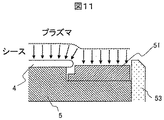
前記フォーカスリングの下面に面し該フォーカスリングの下方でリング状に配置されその内部に熱伝達ガスが導入される溝と、前記フォーカスリングの下方の前記基板ステージの内部に同心状に配置されその内部に冷媒が供給されて循環する通路とを有し、
前記フォーカスリングへの高周波バイアス電力の印加時間を記憶する記憶媒体と、
この記憶された印加時間に応じて、フォーカスリングに分配される高周波電力を増大させるように前記電力分配手段を制御すると共に、前記熱伝達ガスの圧力を増大させる又は前記冷媒の温度を低下させることの少なくとも一方を制御する制御手段を設けたことを特徴とする。
前記基板ステージには、プラズマ生成用高周波電力とは異なる所定の高周波バイアス電力が高周波バイアス電源より印加され、
前記被処理基板が載置される前記基板ステージの上面の周辺に配置されたフォーカスリングには、前記高周波バイアス電源より出力された高周波バイアス電力が電力分配手段によって分配されて印加され、
前記フォーカスリングの下面に面し該フォーカスリングの下方でリング状に配置された溝の内部には熱伝達ガスが導入され、前記フォーカスリングの下方の前記基板ステージの内部に同心状に配置された通路の内部には冷媒が供給されて循環され、
前記プラズマ処理における前記フォーカスリングに印加される前記高周波バイアス電力の大きさを当該フォーカスリングへの高周波バイアス電力の印加時間に応じて、前記電力分配手段により増大するように調節する一方、
前記基板ステージに印加する前記高周波バイアス電力を前記高周波バイアス電源の出力で制御し、
前記フォーカスリングに印加する高周波バイアス電力に応じて、前記フォーカスリングが所定温度となるように制御されることを特徴とする。
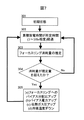
次に、(b)高周波バイアス電源11を制御して全体のバイアス電力を所定の値に上昇させる。これは、フォーカスリングへのバイアス電力の増加分を補って、基板ステージ5への印加電力を所定値確保してエッチング特性を維持するためである。
次いで、(c)フォーカスリングへ分配されたバイアス電力に対応して伝熱ガス導入機構23を制御し、伝熱ガス溝63の伝熱ガス圧力を所定の値に上昇させる。
続いて(d)フォーカスリングへ分配されたバイアス電力に対応して温調機22を制御し、第二冷媒溝58の冷媒温度を所定の値に低下させる。
Claims (4)
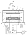
- 真空排気手段により排気された真空容器と、この真空容器にガスを供給するためのガス供給手段と、前記真空容器内にプラズマを形成するための高周波電源と、被処理基板及びこの基板の外周部に配置されたフォーカスリングとをその上方に載せる基板ステージと、前記基板ステージに高周波バイアス電力を印加する高周波バイアス電源と、前記高周波バイアス電源から出力された高周波バイアス電力の一部を前記フォーカスリングに分配して印加する電力分配手段とを備えたプラズマ処理装置において、
前記フォーカスリングの下面に面し該フォーカスリングの下方でリング状に配置されその内部に熱伝達ガスが導入される溝と、前記フォーカスリングの下方の前記基板ステージの内部に同心状に配置されその内部に冷媒が供給されて循環する通路とを有し、
前記フォーカスリングへの高周波バイアス電力の印加時間を記憶する記憶媒体と、
この記憶された印加時間に応じて、前記フォーカスリングに分配される高周波電力を増大させるように前記電力分配手段を制御すると共に、前記熱伝達ガスの圧力を増大させる又は前記冷媒の温度を低下させることの少なくとも一方を行う制御手段とを設けたことを特徴としたプラズマ処理装置。 - 請求項1記載のプラズマ処理装置において、前記フォーカスリングの下部に静電吸着層と電極層及び絶縁層を一体で形成し、前記静電吸着層とフォーカスリングとの間に前記熱伝達ガスが導入される溝を備えたことを特徴としたプラズマ処理装置。
- 請求項1記載のプラズマ処理装置において、前記フォーカスリングの下部に電極リングと、その下部に絶縁リングを備え、前記絶縁リングの上面に溶射により静電吸着層を形成し、前記フォーカスリング下面と前記静電吸着層の上面との間、前記電極リング下面と前記絶縁リング上面との間、および前記絶縁リング下面と基板ステージの基材外周部の上面との間に、熱伝達ガスを介在させることを特徴としたプラズマ処理装置。
- 真空容器内にガスを供給して基板ステージの上面に載置された被処理基板をプラズマ処理するプラズマ処理方法において、
前記基板ステージには、プラズマ生成用高周波電源とは異なる所定の高周波バイアス電力が高周波バイアス電源より印加され、
前記被処理基板が載置される前記基板ステージの上面の周辺に配置されたフォーカスリングには、前記高周波バイアス電源より出力された前記高周波バイアス電力が電力分配手段により分配されて印加され、
前記フォーカスリングの下面に面し該フォーカスリングの下方でリング状に配置された溝の内部には熱伝達ガスが導入され、前記フォーカスリングの下方の前記基板ステージの内部に同心状に配置された通路の内部には冷媒が供給されて循環され、
前記プラズマ処理における前記フォーカスリングに印加される前記高周波バイアス電力の大きさを当該フォーカスリングへの高周波バイアス電力の印加時間に応じて、前記電力分配手段により増大するように調節する一方、
前記基板ステージに印加する前記高周波バイアス電力を前記高周波バイアス電源の出力で調節し、
前記フォーカスリングに印加する前記高周波バイアス電力に応じて、前記フォーカスリングの温度を所定の値となるように調節するプラズマ処理方法。
Priority Applications (3)
| Application Number | Priority Date | Filing Date | Title |
|---|---|---|---|
| JP2009149772A JP5357639B2 (ja) | 2009-06-24 | 2009-06-24 | プラズマ処理装置およびプラズマ処理方法 |
| US12/538,201 US20100326957A1 (en) | 2009-06-24 | 2009-08-10 | Plasma processing apparatus and plasma processing method |
| KR1020090074177A KR101066974B1 (ko) | 2009-06-24 | 2009-08-12 | 플라즈마처리장치 및 플라즈마처리방법 |
Applications Claiming Priority (1)
| Application Number | Priority Date | Filing Date | Title |
|---|---|---|---|
| JP2009149772A JP5357639B2 (ja) | 2009-06-24 | 2009-06-24 | プラズマ処理装置およびプラズマ処理方法 |
Publications (3)
| Publication Number | Publication Date |
|---|---|
| JP2011009351A JP2011009351A (ja) | 2011-01-13 |
| JP2011009351A5 JP2011009351A5 (ja) | 2012-07-05 |
| JP5357639B2 true JP5357639B2 (ja) | 2013-12-04 |
Family
ID=43379587
Family Applications (1)
| Application Number | Title | Priority Date | Filing Date |
|---|---|---|---|
| JP2009149772A Expired - Fee Related JP5357639B2 (ja) | 2009-06-24 | 2009-06-24 | プラズマ処理装置およびプラズマ処理方法 |
Country Status (3)
| Country | Link |
|---|---|
| US (1) | US20100326957A1 (ja) |
| JP (1) | JP5357639B2 (ja) |
| KR (1) | KR101066974B1 (ja) |
Families Citing this family (127)
| Publication number | Priority date | Publication date | Assignee | Title |
|---|---|---|---|---|
| JP5198226B2 (ja) * | 2008-11-20 | 2013-05-15 | 東京エレクトロン株式会社 | 基板載置台および基板処理装置 |
| US8486221B2 (en) | 2009-02-05 | 2013-07-16 | Tokyo Electron Limited | Focus ring heating method, plasma etching apparatus, and plasma etching method |
| JP5730521B2 (ja) * | 2010-09-08 | 2015-06-10 | 株式会社日立ハイテクノロジーズ | 熱処理装置 |
| JP5690596B2 (ja) * | 2011-01-07 | 2015-03-25 | 東京エレクトロン株式会社 | フォーカスリング及び該フォーカスリングを備える基板処理装置 |
| JP5732941B2 (ja) * | 2011-03-16 | 2015-06-10 | 東京エレクトロン株式会社 | プラズマエッチング装置及びプラズマエッチング方法 |
| JP6085079B2 (ja) * | 2011-03-28 | 2017-02-22 | 東京エレクトロン株式会社 | パターン形成方法、処理容器内の部材の温度制御方法、及び基板処理システム |
| JP5822578B2 (ja) * | 2011-07-20 | 2015-11-24 | 東京エレクトロン株式会社 | 載置台温度制御装置及び基板処理装置 |
| US20130107415A1 (en) * | 2011-10-28 | 2013-05-02 | Applied Materials, Inc. | Electrostatic chuck |
| US9947559B2 (en) * | 2011-10-28 | 2018-04-17 | Applied Materials, Inc. | Thermal management of edge ring in semiconductor processing |
| US9412579B2 (en) * | 2012-04-26 | 2016-08-09 | Applied Materials, Inc. | Methods and apparatus for controlling substrate uniformity |
| CN103377979B (zh) | 2012-04-30 | 2016-06-08 | 细美事有限公司 | 调节板和具有该调节板的用于处理基板的装置 |
| KR101974420B1 (ko) | 2012-06-08 | 2019-05-02 | 세메스 주식회사 | 기판처리장치 및 방법 |
| KR101955575B1 (ko) | 2012-06-08 | 2019-03-08 | 세메스 주식회사 | 기판처리장치 및 방법 |
| KR101974422B1 (ko) | 2012-06-27 | 2019-05-02 | 세메스 주식회사 | 기판처리장치 및 방법 |
| JP5982206B2 (ja) * | 2012-07-17 | 2016-08-31 | 東京エレクトロン株式会社 | 下部電極、及びプラズマ処理装置 |
| CN103972132B (zh) * | 2013-01-24 | 2017-07-11 | 东京毅力科创株式会社 | 基板处理装置和载置台 |
| JP6100564B2 (ja) * | 2013-01-24 | 2017-03-22 | 東京エレクトロン株式会社 | 基板処理装置及び載置台 |
| US9236305B2 (en) * | 2013-01-25 | 2016-01-12 | Applied Materials, Inc. | Wafer dicing with etch chamber shield ring for film frame wafer applications |
| JP6080571B2 (ja) * | 2013-01-31 | 2017-02-15 | 東京エレクトロン株式会社 | 載置台及びプラズマ処理装置 |
| JP5971144B2 (ja) * | 2013-02-06 | 2016-08-17 | 東京エレクトロン株式会社 | 基板処理装置及び成膜方法 |
| JP6173936B2 (ja) * | 2013-02-28 | 2017-08-02 | 東京エレクトロン株式会社 | 載置台及びプラズマ処理装置 |
| KR102112368B1 (ko) | 2013-02-28 | 2020-05-18 | 도쿄엘렉트론가부시키가이샤 | 탑재대 및 플라즈마 처리 장치 |
| JP6027492B2 (ja) * | 2013-05-22 | 2016-11-16 | 東京エレクトロン株式会社 | エッチング方法及びエッチング装置 |
| JP6224366B2 (ja) * | 2013-07-12 | 2017-11-01 | 東京エレクトロン株式会社 | 支持部材及び基板処理装置 |
| JP6083529B2 (ja) * | 2013-09-02 | 2017-02-22 | パナソニックIpマネジメント株式会社 | プラズマ処理装置及びプラズマ処理方法 |
| US10002744B2 (en) * | 2013-12-17 | 2018-06-19 | Tokyo Electron Limited | System and method for controlling plasma density |
| JP6442296B2 (ja) * | 2014-06-24 | 2018-12-19 | 東京エレクトロン株式会社 | 載置台及びプラズマ処理装置 |
| TWI603416B (zh) | 2014-07-08 | 2017-10-21 | 瓦特洛威電子製造公司 | 具有接合層之整合溫度感測技術的接合總成 |
| US9530626B2 (en) * | 2014-07-25 | 2016-12-27 | Tokyo Electron Limited | Method and apparatus for ESC charge control for wafer clamping |
| CN104269370B (zh) * | 2014-09-01 | 2017-05-17 | 上海华力微电子有限公司 | 改善晶圆边缘缺陷的装置 |
| US10262886B2 (en) * | 2014-09-30 | 2019-04-16 | Sumitomo Osaka Cement Co., Ltd. | Electrostatic chuck device |
| US9873180B2 (en) | 2014-10-17 | 2018-01-23 | Applied Materials, Inc. | CMP pad construction with composite material properties using additive manufacturing processes |
| KR20240015167A (ko) | 2014-10-17 | 2024-02-02 | 어플라이드 머티어리얼스, 인코포레이티드 | 애디티브 제조 프로세스들을 이용한 복합 재료 특성들을 갖는 cmp 패드 구성 |
| US11745302B2 (en) | 2014-10-17 | 2023-09-05 | Applied Materials, Inc. | Methods and precursor formulations for forming advanced polishing pads by use of an additive manufacturing process |
| US10875153B2 (en) | 2014-10-17 | 2020-12-29 | Applied Materials, Inc. | Advanced polishing pad materials and formulations |
| US9776361B2 (en) | 2014-10-17 | 2017-10-03 | Applied Materials, Inc. | Polishing articles and integrated system and methods for manufacturing chemical mechanical polishing articles |
| JP5798677B2 (ja) * | 2014-10-29 | 2015-10-21 | 東京エレクトロン株式会社 | 基板処理装置及び基板処理方法 |
| US10109510B2 (en) * | 2014-12-18 | 2018-10-23 | Varian Semiconductor Equipment Associates, Inc. | Apparatus for improving temperature uniformity of a workpiece |
| US9909197B2 (en) * | 2014-12-22 | 2018-03-06 | Semes Co., Ltd. | Supporting unit and substrate treating apparatus including the same |
| JP6346855B2 (ja) | 2014-12-25 | 2018-06-20 | 東京エレクトロン株式会社 | 静電吸着方法及び基板処理装置 |
| JP6452449B2 (ja) * | 2015-01-06 | 2019-01-16 | 東京エレクトロン株式会社 | 載置台及び基板処理装置 |
| JP6539113B2 (ja) | 2015-05-28 | 2019-07-03 | 株式会社日立ハイテクノロジーズ | プラズマ処理装置およびプラズマ処理方法 |
| US10163610B2 (en) * | 2015-07-13 | 2018-12-25 | Lam Research Corporation | Extreme edge sheath and wafer profile tuning through edge-localized ion trajectory control and plasma operation |
| US10593574B2 (en) | 2015-11-06 | 2020-03-17 | Applied Materials, Inc. | Techniques for combining CMP process tracking data with 3D printed CMP consumables |
| CN106856188B (zh) * | 2015-12-08 | 2020-02-14 | 北京北方华创微电子装备有限公司 | 承载装置以及半导体加工设备 |
| US10391605B2 (en) | 2016-01-19 | 2019-08-27 | Applied Materials, Inc. | Method and apparatus for forming porous advanced polishing pads using an additive manufacturing process |
| US10685862B2 (en) * | 2016-01-22 | 2020-06-16 | Applied Materials, Inc. | Controlling the RF amplitude of an edge ring of a capacitively coupled plasma process device |
| KR102604063B1 (ko) | 2016-08-18 | 2023-11-21 | 삼성전자주식회사 | 정전 척 어셈블리 및 이를 포함하는 기판 처리 장치 |
| US9922857B1 (en) | 2016-11-03 | 2018-03-20 | Lam Research Corporation | Electrostatically clamped edge ring |
| US10535505B2 (en) * | 2016-11-11 | 2020-01-14 | Lam Research Corporation | Plasma light up suppression |
| KR102581226B1 (ko) * | 2016-12-23 | 2023-09-20 | 삼성전자주식회사 | 플라즈마 처리 장치 |
| JP6340655B2 (ja) * | 2017-01-10 | 2018-06-13 | パナソニックIpマネジメント株式会社 | プラズマ処理装置及びプラズマ処理方法 |
| JP6869034B2 (ja) * | 2017-01-17 | 2021-05-12 | 東京エレクトロン株式会社 | プラズマ処理装置 |
| WO2018183245A1 (en) * | 2017-03-31 | 2018-10-04 | Mattson Technology, Inc. | Material deposition prevention on a workpiece in a process chamber |
| US10199252B2 (en) * | 2017-06-30 | 2019-02-05 | Taiwan Semiconductor Manufacturing Company, Ltd. | Thermal pad for etch rate uniformity |
| CN109216144B (zh) * | 2017-07-03 | 2021-08-06 | 中微半导体设备(上海)股份有限公司 | 一种具有低频射频功率分布调节功能的等离子反应器 |
| US11471999B2 (en) | 2017-07-26 | 2022-10-18 | Applied Materials, Inc. | Integrated abrasive polishing pads and manufacturing methods |
| US10510575B2 (en) | 2017-09-20 | 2019-12-17 | Applied Materials, Inc. | Substrate support with multiple embedded electrodes |
| JP6518024B1 (ja) * | 2017-10-30 | 2019-05-22 | 日本碍子株式会社 | 静電チャック及びその製法 |
| JP7033441B2 (ja) | 2017-12-01 | 2022-03-10 | 東京エレクトロン株式会社 | プラズマ処理装置 |
| CN111466009B (zh) * | 2017-12-15 | 2023-07-07 | 朗姆研究公司 | 等离子体室中使用的环形结构和系统 |
| JP7033907B2 (ja) * | 2017-12-21 | 2022-03-11 | 東京エレクトロン株式会社 | プラズマエッチング装置及びプラズマエッチング方法 |
| JP7149068B2 (ja) * | 2017-12-21 | 2022-10-06 | 株式会社日立ハイテク | プラズマ処理装置およびプラズマ処理方法 |
| CN109994355B (zh) | 2017-12-29 | 2021-11-02 | 中微半导体设备(上海)股份有限公司 | 一种具有低频射频功率分布调节功能的等离子反应器 |
| CN111095523A (zh) * | 2018-01-22 | 2020-05-01 | 应用材料公司 | 利用经供电的边缘环的处理 |
| JP7140183B2 (ja) * | 2018-02-20 | 2022-09-21 | 住友大阪セメント株式会社 | 静電チャック装置および静電チャック装置の製造方法 |
| US10555412B2 (en) | 2018-05-10 | 2020-02-04 | Applied Materials, Inc. | Method of controlling ion energy distribution using a pulse generator with a current-return output stage |
| JP7204350B2 (ja) * | 2018-06-12 | 2023-01-16 | 東京エレクトロン株式会社 | 載置台、基板処理装置及びエッジリング |
| US10847347B2 (en) * | 2018-08-23 | 2020-11-24 | Applied Materials, Inc. | Edge ring assembly for a substrate support in a plasma processing chamber |
| KR20210042171A (ko) | 2018-09-04 | 2021-04-16 | 어플라이드 머티어리얼스, 인코포레이티드 | 진보한 폴리싱 패드들을 위한 제형들 |
| JP7140610B2 (ja) * | 2018-09-06 | 2022-09-21 | 株式会社日立ハイテク | プラズマ処理装置 |
| JP7175160B2 (ja) * | 2018-11-05 | 2022-11-18 | 東京エレクトロン株式会社 | 基板処理装置 |
| JP7145042B2 (ja) * | 2018-11-08 | 2022-09-30 | 東京エレクトロン株式会社 | 基板支持器及びプラズマ処理装置 |
| JP7145041B2 (ja) * | 2018-11-08 | 2022-09-30 | 東京エレクトロン株式会社 | 基板支持器、プラズマ処理装置、及びフォーカスリング |
| US11476145B2 (en) | 2018-11-20 | 2022-10-18 | Applied Materials, Inc. | Automatic ESC bias compensation when using pulsed DC bias |
| US11289310B2 (en) * | 2018-11-21 | 2022-03-29 | Applied Materials, Inc. | Circuits for edge ring control in shaped DC pulsed plasma process device |
| KR20250100790A (ko) | 2019-01-22 | 2025-07-03 | 어플라이드 머티어리얼스, 인코포레이티드 | 펄스 전압 파형을 제어하기 위한 피드백 루프 |
| US11508554B2 (en) | 2019-01-24 | 2022-11-22 | Applied Materials, Inc. | High voltage filter assembly |
| JP7254542B2 (ja) * | 2019-02-01 | 2023-04-10 | 東京エレクトロン株式会社 | 載置台及び基板処理装置 |
| KR102370471B1 (ko) * | 2019-02-08 | 2022-03-03 | 주식회사 히타치하이테크 | 플라스마 처리 장치 |
| JP2020155489A (ja) * | 2019-03-18 | 2020-09-24 | キオクシア株式会社 | 半導体製造装置および半導体装置の製造方法 |
| US11450545B2 (en) * | 2019-04-17 | 2022-09-20 | Samsung Electronics Co., Ltd. | Capacitively-coupled plasma substrate processing apparatus including a focus ring and a substrate processing method using the same |
| WO2020255319A1 (ja) | 2019-06-20 | 2020-12-24 | 株式会社日立ハイテク | プラズマ処理装置およびプラズマ処理方法 |
| KR102200315B1 (ko) * | 2019-07-29 | 2021-01-08 | 세메스 주식회사 | 기판 지지 장치 및 이를 포함하는 기판 처리 장치 |
| JP7394556B2 (ja) * | 2019-08-09 | 2023-12-08 | 東京エレクトロン株式会社 | 載置台及び基板処理装置 |
| JP7365815B2 (ja) * | 2019-08-09 | 2023-10-20 | 東京エレクトロン株式会社 | 載置台及び基板処理装置 |
| CN112435912B (zh) * | 2019-08-26 | 2023-09-29 | 中微半导体设备(上海)股份有限公司 | 等离子体处理装置 |
| KR102335472B1 (ko) * | 2019-09-04 | 2021-12-07 | 세메스 주식회사 | 기판 처리 장치 및 기판 처리 방법 |
| JP7474651B2 (ja) * | 2019-09-09 | 2024-04-25 | 東京エレクトロン株式会社 | プラズマ処理装置 |
| JP7373963B2 (ja) * | 2019-10-01 | 2023-11-06 | 東京エレクトロン株式会社 | 基板支持器及びプラズマ処理装置 |
| US12266511B2 (en) | 2019-11-26 | 2025-04-01 | Tokyo Electron Limited | Substrate support and substrate processing apparatus |
| JP7563843B2 (ja) * | 2019-11-26 | 2024-10-08 | 東京エレクトロン株式会社 | 載置台及び基板処理装置 |
| JP7043617B2 (ja) * | 2019-12-18 | 2022-03-29 | 株式会社日立ハイテク | プラズマ処理装置 |
| JP7454961B2 (ja) * | 2020-03-05 | 2024-03-25 | 東京エレクトロン株式会社 | プラズマ処理装置 |
| KR102827753B1 (ko) * | 2020-04-07 | 2025-07-02 | 삼성디스플레이 주식회사 | 표시 장치의 제조방법 |
| KR102495233B1 (ko) * | 2020-07-03 | 2023-02-06 | 주식회사 동원파츠 | 정전척 |
| US11462388B2 (en) | 2020-07-31 | 2022-10-04 | Applied Materials, Inc. | Plasma processing assembly using pulsed-voltage and radio-frequency power |
| JP7598225B2 (ja) * | 2020-11-09 | 2024-12-11 | 日本放送協会 | 接合用治具、および接合方法 |
| US11798790B2 (en) | 2020-11-16 | 2023-10-24 | Applied Materials, Inc. | Apparatus and methods for controlling ion energy distribution |
| US11901157B2 (en) | 2020-11-16 | 2024-02-13 | Applied Materials, Inc. | Apparatus and methods for controlling ion energy distribution |
| KR102889019B1 (ko) * | 2020-11-25 | 2025-11-20 | 세메스 주식회사 | 에지 링 어셈블리 및 기판 처리 장치 |
| CN114843165A (zh) * | 2021-02-01 | 2022-08-02 | 中微半导体设备(上海)股份有限公司 | 一种下电极组件及等离子体处理装置 |
| KR102679639B1 (ko) * | 2021-03-24 | 2024-07-01 | 주식회사 히타치하이테크 | 플라스마 처리 장치 및 플라스마 처리 방법 |
| US11495470B1 (en) | 2021-04-16 | 2022-11-08 | Applied Materials, Inc. | Method of enhancing etching selectivity using a pulsed plasma |
| US11791138B2 (en) | 2021-05-12 | 2023-10-17 | Applied Materials, Inc. | Automatic electrostatic chuck bias compensation during plasma processing |
| US11948780B2 (en) | 2021-05-12 | 2024-04-02 | Applied Materials, Inc. | Automatic electrostatic chuck bias compensation during plasma processing |
| JP7557429B2 (ja) * | 2021-05-27 | 2024-09-27 | 東京エレクトロン株式会社 | プラズマ処理装置 |
| US11967483B2 (en) | 2021-06-02 | 2024-04-23 | Applied Materials, Inc. | Plasma excitation with ion energy control |
| US12148595B2 (en) | 2021-06-09 | 2024-11-19 | Applied Materials, Inc. | Plasma uniformity control in pulsed DC plasma chamber |
| US12525433B2 (en) | 2021-06-09 | 2026-01-13 | Applied Materials, Inc. | Method and apparatus to reduce feature charging in plasma processing chamber |
| US12525441B2 (en) | 2021-06-09 | 2026-01-13 | Applied Materials, Inc. | Plasma chamber and chamber component cleaning methods |
| US11810760B2 (en) | 2021-06-16 | 2023-11-07 | Applied Materials, Inc. | Apparatus and method of ion current compensation |
| US11569066B2 (en) | 2021-06-23 | 2023-01-31 | Applied Materials, Inc. | Pulsed voltage source for plasma processing applications |
| US11776788B2 (en) | 2021-06-28 | 2023-10-03 | Applied Materials, Inc. | Pulsed voltage boost for substrate processing |
| CN115565841B (zh) * | 2021-07-02 | 2025-08-08 | 中微半导体设备(上海)股份有限公司 | 防止电弧放电的下电极组件、等离子体处理装置及方法 |
| KR102895924B1 (ko) * | 2021-07-28 | 2025-12-04 | 세메스 주식회사 | 기판 처리 장치 |
| US11476090B1 (en) | 2021-08-24 | 2022-10-18 | Applied Materials, Inc. | Voltage pulse time-domain multiplexing |
| TW202329192A (zh) * | 2021-08-27 | 2023-07-16 | 日商東京威力科創股份有限公司 | 基板支持器及電漿處理裝置 |
| US12106938B2 (en) | 2021-09-14 | 2024-10-01 | Applied Materials, Inc. | Distortion current mitigation in a radio frequency plasma processing chamber |
| JP7496343B2 (ja) * | 2021-11-08 | 2024-06-06 | 日本碍子株式会社 | ウエハ載置台 |
| US11694876B2 (en) | 2021-12-08 | 2023-07-04 | Applied Materials, Inc. | Apparatus and method for delivering a plurality of waveform signals during plasma processing |
| US11972924B2 (en) | 2022-06-08 | 2024-04-30 | Applied Materials, Inc. | Pulsed voltage source for plasma processing applications |
| US12315732B2 (en) | 2022-06-10 | 2025-05-27 | Applied Materials, Inc. | Method and apparatus for etching a semiconductor substrate in a plasma etch chamber |
| US12272524B2 (en) | 2022-09-19 | 2025-04-08 | Applied Materials, Inc. | Wideband variable impedance load for high volume manufacturing qualification and on-site diagnostics |
| US12111341B2 (en) | 2022-10-05 | 2024-10-08 | Applied Materials, Inc. | In-situ electric field detection method and apparatus |
| KR102760072B1 (ko) | 2022-10-07 | 2025-01-24 | 도쿄엘렉트론가부시키가이샤 | 기판 처리 시스템 및 엣지 링의 장착 방법 |
| JP7670876B1 (ja) | 2024-01-15 | 2025-04-30 | 日本特殊陶業株式会社 | 半導体基板処理用基台、セラミックス基材、および製造方法 |
Family Cites Families (10)
| Publication number | Priority date | Publication date | Assignee | Title |
|---|---|---|---|---|
| JP3066007B2 (ja) * | 1998-06-24 | 2000-07-17 | 株式会社日立製作所 | プラズマ処理装置およびプラズマ処理方法 |
| JP2000183038A (ja) | 1998-12-14 | 2000-06-30 | Hitachi Ltd | プラズマ処理装置 |
| US20040261945A1 (en) * | 2002-10-02 | 2004-12-30 | Ensinger Kunststofftechnoligie Gbr | Retaining ring for holding semiconductor wafers in a chemical mechanical polishing apparatus |
| JP4547182B2 (ja) * | 2003-04-24 | 2010-09-22 | 東京エレクトロン株式会社 | プラズマ処理装置 |
| JP2006216822A (ja) | 2005-02-04 | 2006-08-17 | Hitachi High-Technologies Corp | ウェハ処理装置およびウェハ処理方法 |
| JP2006319043A (ja) * | 2005-05-11 | 2006-11-24 | Hitachi High-Technologies Corp | プラズマ処理装置 |
| JP2006351887A (ja) * | 2005-06-17 | 2006-12-28 | Hitachi High-Technologies Corp | プラズマ処理装置 |
| JP4972327B2 (ja) | 2006-03-22 | 2012-07-11 | 東京エレクトロン株式会社 | プラズマ処理装置 |
| JP2007258500A (ja) * | 2006-03-24 | 2007-10-04 | Hitachi High-Technologies Corp | 基板支持装置 |
| JP2008251866A (ja) * | 2007-03-30 | 2008-10-16 | Hitachi High-Technologies Corp | プラズマ処理装置 |
-
2009
- 2009-06-24 JP JP2009149772A patent/JP5357639B2/ja not_active Expired - Fee Related
- 2009-08-10 US US12/538,201 patent/US20100326957A1/en not_active Abandoned
- 2009-08-12 KR KR1020090074177A patent/KR101066974B1/ko not_active Expired - Fee Related
Also Published As
| Publication number | Publication date |
|---|---|
| KR20100138687A (ko) | 2010-12-31 |
| JP2011009351A (ja) | 2011-01-13 |
| KR101066974B1 (ko) | 2011-09-22 |
| US20100326957A1 (en) | 2010-12-30 |
Similar Documents
| Publication | Publication Date | Title |
|---|---|---|
| JP5357639B2 (ja) | プラズマ処理装置およびプラズマ処理方法 | |
| JP7662489B2 (ja) | 極めて均一性が高い加熱基板支持アセンブリ | |
| JP7169319B2 (ja) | ガス孔に開口縮小プラグを有する大電力静電チャック | |
| US8520360B2 (en) | Electrostatic chuck with wafer backside plasma assisted dechuck | |
| JP4909424B2 (ja) | 静電チャック | |
| CN101425474B (zh) | 提供减小等离子体穿透和电弧的静电夹盘的方法和设备 | |
| KR101265807B1 (ko) | 개선된 반도체 프로세싱 균일성을 위한 열 전송 시스템 | |
| US20100122774A1 (en) | Substrate mounting table and substrate processing apparatus having same | |
| JP6283532B2 (ja) | 静電チャックの製造方法 | |
| JP4674792B2 (ja) | 静電チャック | |
| JP2008251742A (ja) | 基板処理装置及びフォーカスリングを載置する基板載置台 | |
| CN111048462B (zh) | 基板支承装置及其制造方法 | |
| JP7799248B2 (ja) | 静電チャック | |
| JP7486018B2 (ja) | 静電チャック | |
| JP2005347400A (ja) | 静電吸着装置およびプラズマ処理装置 | |
| JP5086206B2 (ja) | プラズマ処理装置 | |
| JP7484152B2 (ja) | 静電チャック | |
| US20040000375A1 (en) | Plasma etch chamber equipped with multi-layer insert ring | |
| JP2025526053A (ja) | 静電チャック用真空シール | |
| WO2025240127A1 (en) | Substrate support heat transfer structures | |
| KR20250155334A (ko) | 기판 처리 장치 및 기판 처리 방법 | |
| TW202226739A (zh) | 靜電吸盤、下電極元件及等離子體處理裝置 | |
| KR20180025598A (ko) | 기판 지지 유닛 및 이를 가지는 기판 처리 장치 |
Legal Events
| Date | Code | Title | Description |
|---|---|---|---|
| A521 | Request for written amendment filed |
Free format text: JAPANESE INTERMEDIATE CODE: A523 Effective date: 20120522 |
|
| A621 | Written request for application examination |
Free format text: JAPANESE INTERMEDIATE CODE: A621 Effective date: 20120522 |
|
| A131 | Notification of reasons for refusal |
Free format text: JAPANESE INTERMEDIATE CODE: A131 Effective date: 20130129 |
|
| A977 | Report on retrieval |
Free format text: JAPANESE INTERMEDIATE CODE: A971007 Effective date: 20130131 |
|
| A521 | Request for written amendment filed |
Free format text: JAPANESE INTERMEDIATE CODE: A523 Effective date: 20130327 |
|
| A131 | Notification of reasons for refusal |
Free format text: JAPANESE INTERMEDIATE CODE: A131 Effective date: 20130507 |
|
| A521 | Request for written amendment filed |
Free format text: JAPANESE INTERMEDIATE CODE: A523 Effective date: 20130703 |
|
| TRDD | Decision of grant or rejection written | ||
| A01 | Written decision to grant a patent or to grant a registration (utility model) |
Free format text: JAPANESE INTERMEDIATE CODE: A01 Effective date: 20130806 |
|
| A61 | First payment of annual fees (during grant procedure) |
Free format text: JAPANESE INTERMEDIATE CODE: A61 Effective date: 20130830 |
|
| R150 | Certificate of patent or registration of utility model |
Ref document number: 5357639 Country of ref document: JP Free format text: JAPANESE INTERMEDIATE CODE: R150 Free format text: JAPANESE INTERMEDIATE CODE: R150 |
|
| S531 | Written request for registration of change of domicile |
Free format text: JAPANESE INTERMEDIATE CODE: R313531 |
|
| S533 | Written request for registration of change of name |
Free format text: JAPANESE INTERMEDIATE CODE: R313533 |
|
| R350 | Written notification of registration of transfer |
Free format text: JAPANESE INTERMEDIATE CODE: R350 |
|
| LAPS | Cancellation because of no payment of annual fees |