JP4674792B2 - 静電チャック - Google Patents
静電チャック Download PDFInfo
- Publication number
- JP4674792B2 JP4674792B2 JP2004351448A JP2004351448A JP4674792B2 JP 4674792 B2 JP4674792 B2 JP 4674792B2 JP 2004351448 A JP2004351448 A JP 2004351448A JP 2004351448 A JP2004351448 A JP 2004351448A JP 4674792 B2 JP4674792 B2 JP 4674792B2
- Authority
- JP
- Japan
- Prior art keywords
- electrostatic chuck
- wafer
- protrusion
- temperature
- protrusions
- Prior art date
- Legal status (The legal status is an assumption and is not a legal conclusion. Google has not performed a legal analysis and makes no representation as to the accuracy of the status listed.)
- Expired - Fee Related
Links
Images


Landscapes
- Drying Of Semiconductors (AREA)
- Container, Conveyance, Adherence, Positioning, Of Wafer (AREA)
Description
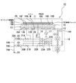
本実施形態のプラズマ処理装置10は、例えば図1に示すように、高真空を保持し得るチャンバー11と、このチャンバー11内に配置され且つ被吸着基板(例えば、ウエハ)Wを載置する載置体12と、この載置体12をチャンバー11から電気的に絶縁する絶縁体13とを備え、チャンバー11に排気管14Aを介して接続された真空排気系14によって所定の真空度を保持したチャンバー11内でウエハWに対して所定のプラズマ処理を施すように構成されている。
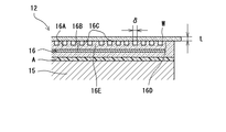
16A セラミック誘電体
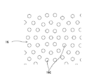
16C 突起部
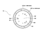
16D 第1の環状突起部
16E 第2の環状突起部
16H 第1のガス供給口
16I 第2のガス供給口
Claims (7)
- 静電気力を使用して被吸着基板を吸着する静電チャックであって、
上記静電チャックは、
上記被吸着基板と接触する複数の突起部を有し且つ上記突起部が所定の粒径を有する結晶粒子を含むセラミック誘電体によって形成されていると共に、上記複数の突起部の上記被吸着基板との接触面を、プラズマによるドライクリーニングによって表面処理することにより上記粒径に依存して最終的に安定する一定の表面粗度に形成してなり、且つ、
上記セラミック誘電体が酸化アルミニウムを主成分とするものであり、
上記所定の粒径が1〜2μmであり、
上記接触面の表面粗度がRa0.2〜0.3μmである
ことを特徴とする静電チャック。 - 上記セラミック誘電体は、炭化珪素を含むことを特徴とする請求項1に記載の静電チャック。
- 上記突起部の硬度を、ヴィッカース硬度でHv2000以上に設定したことを特徴とする請求項1または請求項2に記載の静電チャック。
- 上記複数の突起部の上記被吸着基板の単位面積当たりの接触面積比率を、15%以下に設定したことを特徴する請求項1〜請求項3のいずれか1項に記載の静電チャック。
- 上記突起部を、直径が0.5mm以下の円柱状の突起として形成したことを特徴とする請求項4に記載の静電チャック。
- 上記複数の突起部間の距離を、1mm以下に設定したことを特徴とする請求項4または請求項5に記載の静電チャック。
- 上記突起部の高さを、30μm以上に設定したことを特徴とする請求項4〜請求項6のいずれか1項に記載の静電チャック。
Priority Applications (1)
| Application Number | Priority Date | Filing Date | Title |
|---|---|---|---|
| JP2004351448A JP4674792B2 (ja) | 2003-12-05 | 2004-12-03 | 静電チャック |
Applications Claiming Priority (2)
| Application Number | Priority Date | Filing Date | Title |
|---|---|---|---|
| JP2003408224 | 2003-12-05 | ||
| JP2004351448A JP4674792B2 (ja) | 2003-12-05 | 2004-12-03 | 静電チャック |
Related Child Applications (2)
| Application Number | Title | Priority Date | Filing Date |
|---|---|---|---|
| JP2010056825A Division JP2010147502A (ja) | 2003-12-05 | 2010-03-13 | 静電チャック |
| JP2010056826A Division JP4909424B2 (ja) | 2003-12-05 | 2010-03-13 | 静電チャック |
Publications (2)
| Publication Number | Publication Date |
|---|---|
| JP2005191561A JP2005191561A (ja) | 2005-07-14 |
| JP4674792B2 true JP4674792B2 (ja) | 2011-04-20 |
Family
ID=34797686
Family Applications (1)
| Application Number | Title | Priority Date | Filing Date |
|---|---|---|---|
| JP2004351448A Expired - Fee Related JP4674792B2 (ja) | 2003-12-05 | 2004-12-03 | 静電チャック |
Country Status (1)
| Country | Link |
|---|---|
| JP (1) | JP4674792B2 (ja) |
Families Citing this family (21)
| Publication number | Priority date | Publication date | Assignee | Title |
|---|---|---|---|---|
| KR100666039B1 (ko) | 2003-12-05 | 2007-01-10 | 동경 엘렉트론 주식회사 | 정전척 |
| JP4690837B2 (ja) * | 2005-09-13 | 2011-06-01 | 株式会社日立ハイテクノロジーズ | 試料載置電極の温度制御方法及び温度制御装置 |
| JP4622764B2 (ja) * | 2005-09-15 | 2011-02-02 | パナソニック株式会社 | プラズマ処理方法 |
| JP2007173596A (ja) * | 2005-12-22 | 2007-07-05 | Ngk Insulators Ltd | 静電チャック |
| JP2007234425A (ja) * | 2006-03-01 | 2007-09-13 | Ngk Insulators Ltd | 加熱装置 |
| US8226769B2 (en) | 2006-04-27 | 2012-07-24 | Applied Materials, Inc. | Substrate support with electrostatic chuck having dual temperature zones |
| JP5069452B2 (ja) | 2006-04-27 | 2012-11-07 | アプライド マテリアルズ インコーポレイテッド | 二重温度帯を有する静電チャックをもつ基板支持体 |
| JP5183058B2 (ja) * | 2006-07-20 | 2013-04-17 | アプライド マテリアルズ インコーポレイテッド | 急速温度勾配コントロールによる基板処理 |
| US9275887B2 (en) | 2006-07-20 | 2016-03-01 | Applied Materials, Inc. | Substrate processing with rapid temperature gradient control |
| JP2008085129A (ja) * | 2006-09-28 | 2008-04-10 | Taiheiyo Cement Corp | 基板載置装置 |
| JP5312765B2 (ja) * | 2007-01-26 | 2013-10-09 | 株式会社日立国際電気 | 基板処理方法及び半導体製造装置 |
| JP5059450B2 (ja) * | 2007-03-06 | 2012-10-24 | 東京エレクトロン株式会社 | 基板載置台及び基板処理装置 |
| US20080225261A1 (en) * | 2007-03-13 | 2008-09-18 | Noriyuki Hirayanagi | Exposure apparatus and device manufacturing method |
| JP5510991B2 (ja) * | 2007-09-06 | 2014-06-04 | 株式会社日立国際電気 | 半導体製造装置及び基板処理方法 |
| JP5390657B2 (ja) * | 2012-05-02 | 2014-01-15 | 東京エレクトロン株式会社 | 基板載置台及び基板処理装置 |
| CN106716619B (zh) * | 2014-09-30 | 2020-09-15 | 住友大阪水泥股份有限公司 | 静电吸盘装置 |
| WO2016052115A1 (ja) * | 2014-09-30 | 2016-04-07 | 住友大阪セメント株式会社 | 静電チャック装置 |
| WO2020231609A1 (en) * | 2019-05-16 | 2020-11-19 | Applied Materials, Inc. | Methods and apparatus for minimizing substrate backside damage |
| WO2023022041A1 (ja) * | 2021-08-20 | 2023-02-23 | 東京エレクトロン株式会社 | 静電チャック、基板支持器及び基板処理装置 |
| JP7572936B2 (ja) * | 2021-11-29 | 2024-10-24 | 日本碍子株式会社 | ウエハ載置台 |
| JP2024075408A (ja) * | 2022-11-22 | 2024-06-03 | 日本特殊陶業株式会社 | セラミックスヒータ |
Family Cites Families (5)
| Publication number | Priority date | Publication date | Assignee | Title |
|---|---|---|---|---|
| JPH0945753A (ja) * | 1995-07-28 | 1997-02-14 | Kyocera Corp | 物品保持装置 |
| JPH11209182A (ja) * | 1998-01-22 | 1999-08-03 | Sumitomo Metal Ind Ltd | プラズマ耐食部材 |
| JP4213790B2 (ja) * | 1998-08-26 | 2009-01-21 | コバレントマテリアル株式会社 | 耐プラズマ部材およびそれを用いたプラズマ処理装置 |
| JP4387563B2 (ja) * | 2000-06-05 | 2009-12-16 | 住友大阪セメント株式会社 | サセプタ及びサセプタの製造方法 |
| JP2002151580A (ja) * | 2000-11-14 | 2002-05-24 | Sumitomo Osaka Cement Co Ltd | ウエハー保持具の製造方法及びウエハー保持具 |
-
2004
- 2004-12-03 JP JP2004351448A patent/JP4674792B2/ja not_active Expired - Fee Related
Also Published As
| Publication number | Publication date |
|---|---|
| JP2005191561A (ja) | 2005-07-14 |
Similar Documents
| Publication | Publication Date | Title |
|---|---|---|
| JP4909424B2 (ja) | 静電チャック | |
| JP4674792B2 (ja) | 静電チャック | |
| JP7662489B2 (ja) | 極めて均一性が高い加熱基板支持アセンブリ | |
| JP5357639B2 (ja) | プラズマ処理装置およびプラズマ処理方法 | |
| JP6489146B2 (ja) | 静電チャック装置 | |
| JP5881419B2 (ja) | 静電クランプおよびワークピースをクランプするための方法 | |
| EP2088616A2 (en) | Substrate mounting table, substrate processing apparatus and substrate temperature control method | |
| US20080236746A1 (en) | Substrate processing apparatus and substrate mounting stage on which focus ring is mounted | |
| US11011405B2 (en) | Apparatus for supporting substrate having gas supply hole and method of manufacturing same | |
| JP2010157559A (ja) | プラズマ処置装置 | |
| US7718007B2 (en) | Substrate supporting member and substrate processing apparatus | |
| JP2016184645A (ja) | 静電チャック装置 | |
| JP4390629B2 (ja) | 静電吸着装置およびプラズマ処理装置 | |
| US11075062B2 (en) | Vacuum processing apparatus | |
| JPH04371579A (ja) | 静電吸着装置 | |
| JP7450348B2 (ja) | 真空処理装置 | |
| JP2025115710A (ja) | 静電チャック |
Legal Events
| Date | Code | Title | Description |
|---|---|---|---|
| A711 | Notification of change in applicant |
Free format text: JAPANESE INTERMEDIATE CODE: A711 Effective date: 20070807 |
|
| A521 | Request for written amendment filed |
Free format text: JAPANESE INTERMEDIATE CODE: A821 Effective date: 20070808 |
|
| A521 | Request for written amendment filed |
Free format text: JAPANESE INTERMEDIATE CODE: A523 Effective date: 20071004 |
|
| A521 | Request for written amendment filed |
Free format text: JAPANESE INTERMEDIATE CODE: A821 Effective date: 20071004 |
|
| A621 | Written request for application examination |
Free format text: JAPANESE INTERMEDIATE CODE: A621 Effective date: 20071201 |
|
| A977 | Report on retrieval |
Free format text: JAPANESE INTERMEDIATE CODE: A971007 Effective date: 20091221 |
|
| A131 | Notification of reasons for refusal |
Free format text: JAPANESE INTERMEDIATE CODE: A131 Effective date: 20100112 |
|
| A521 | Request for written amendment filed |
Free format text: JAPANESE INTERMEDIATE CODE: A523 Effective date: 20100313 |
|
| A131 | Notification of reasons for refusal |
Free format text: JAPANESE INTERMEDIATE CODE: A131 Effective date: 20100907 |
|
| A521 | Request for written amendment filed |
Free format text: JAPANESE INTERMEDIATE CODE: A523 Effective date: 20101104 |
|
| TRDD | Decision of grant or rejection written | ||
| A01 | Written decision to grant a patent or to grant a registration (utility model) |
Free format text: JAPANESE INTERMEDIATE CODE: A01 Effective date: 20110118 |
|
| A01 | Written decision to grant a patent or to grant a registration (utility model) |
Free format text: JAPANESE INTERMEDIATE CODE: A01 |
|
| A61 | First payment of annual fees (during grant procedure) |
Free format text: JAPANESE INTERMEDIATE CODE: A61 Effective date: 20110120 |
|
| FPAY | Renewal fee payment (event date is renewal date of database) |
Free format text: PAYMENT UNTIL: 20140204 Year of fee payment: 3 |
|
| R150 | Certificate of patent or registration of utility model |
Ref document number: 4674792 Country of ref document: JP Free format text: JAPANESE INTERMEDIATE CODE: R150 Free format text: JAPANESE INTERMEDIATE CODE: R150 |
|
| R250 | Receipt of annual fees |
Free format text: JAPANESE INTERMEDIATE CODE: R250 |
|
| R250 | Receipt of annual fees |
Free format text: JAPANESE INTERMEDIATE CODE: R250 |
|
| R250 | Receipt of annual fees |
Free format text: JAPANESE INTERMEDIATE CODE: R250 |
|
| R250 | Receipt of annual fees |
Free format text: JAPANESE INTERMEDIATE CODE: R250 |
|
| R250 | Receipt of annual fees |
Free format text: JAPANESE INTERMEDIATE CODE: R250 |
|
| R250 | Receipt of annual fees |
Free format text: JAPANESE INTERMEDIATE CODE: R250 |
|
| R250 | Receipt of annual fees |
Free format text: JAPANESE INTERMEDIATE CODE: R250 |
|
| R250 | Receipt of annual fees |
Free format text: JAPANESE INTERMEDIATE CODE: R250 |
|
| R250 | Receipt of annual fees |
Free format text: JAPANESE INTERMEDIATE CODE: R250 |
|
| R250 | Receipt of annual fees |
Free format text: JAPANESE INTERMEDIATE CODE: R250 |
|
| LAPS | Cancellation because of no payment of annual fees |