JP7572936B2 - ウエハ載置台 - Google Patents
ウエハ載置台 Download PDFInfo
- Publication number
- JP7572936B2 JP7572936B2 JP2021192899A JP2021192899A JP7572936B2 JP 7572936 B2 JP7572936 B2 JP 7572936B2 JP 2021192899 A JP2021192899 A JP 2021192899A JP 2021192899 A JP2021192899 A JP 2021192899A JP 7572936 B2 JP7572936 B2 JP 7572936B2
- Authority
- JP
- Japan
- Prior art keywords
- flow path
- wafer
- small
- area
- wafer mounting
- Prior art date
- Legal status (The legal status is an assumption and is not a legal conclusion. Google has not performed a legal analysis and makes no representation as to the accuracy of the status listed.)
- Active
Links
- 239000000758 substrate Substances 0.000 claims description 85
- 239000003507 refrigerant Substances 0.000 claims description 76
- 239000000919 ceramic Substances 0.000 claims description 65
- 238000001816 cooling Methods 0.000 claims description 55
- 238000011144 upstream manufacturing Methods 0.000 claims description 47
- 239000000463 material Substances 0.000 claims description 42
- 229910052751 metal Inorganic materials 0.000 claims description 42
- 239000002184 metal Substances 0.000 claims description 42
- 230000002093 peripheral effect Effects 0.000 claims description 38
- 239000011156 metal matrix composite Substances 0.000 claims description 36
- 239000002826 coolant Substances 0.000 claims description 28
- 230000000149 penetrating effect Effects 0.000 claims description 6
- 235000012431 wafers Nutrition 0.000 description 178
- 238000001179 sorption measurement Methods 0.000 description 16
- PNEYBMLMFCGWSK-UHFFFAOYSA-N aluminium oxide Inorganic materials [O-2].[O-2].[O-2].[Al+3].[Al+3] PNEYBMLMFCGWSK-UHFFFAOYSA-N 0.000 description 6
- 238000000034 method Methods 0.000 description 6
- 239000000843 powder Substances 0.000 description 6
- HBMJWWWQQXIZIP-UHFFFAOYSA-N silicon carbide Chemical compound [Si+]#[C-] HBMJWWWQQXIZIP-UHFFFAOYSA-N 0.000 description 6
- 229910010271 silicon carbide Inorganic materials 0.000 description 6
- 229910000962 AlSiC Inorganic materials 0.000 description 4
- 239000010936 titanium Substances 0.000 description 4
- 238000005422 blasting Methods 0.000 description 3
- 238000010586 diagram Methods 0.000 description 3
- 238000000605 extraction Methods 0.000 description 3
- 238000004519 manufacturing process Methods 0.000 description 3
- 229910018566 Al—Si—Mg Inorganic materials 0.000 description 2
- 238000005530 etching Methods 0.000 description 2
- 238000007731 hot pressing Methods 0.000 description 2
- 238000005304 joining Methods 0.000 description 2
- 239000000203 mixture Substances 0.000 description 2
- 239000011347 resin Substances 0.000 description 2
- 229920005989 resin Polymers 0.000 description 2
- 238000005507 spraying Methods 0.000 description 2
- 229910052721 tungsten Inorganic materials 0.000 description 2
- 229910018134 Al-Mg Inorganic materials 0.000 description 1
- 229910018467 Al—Mg Inorganic materials 0.000 description 1
- ZOKXTWBITQBERF-UHFFFAOYSA-N Molybdenum Chemical compound [Mo] ZOKXTWBITQBERF-UHFFFAOYSA-N 0.000 description 1
- RTAQQCXQSZGOHL-UHFFFAOYSA-N Titanium Chemical compound [Ti] RTAQQCXQSZGOHL-UHFFFAOYSA-N 0.000 description 1
- 229910045601 alloy Inorganic materials 0.000 description 1
- 239000000956 alloy Substances 0.000 description 1
- 229910052782 aluminium Inorganic materials 0.000 description 1
- XAGFODPZIPBFFR-UHFFFAOYSA-N aluminium Chemical compound [Al] XAGFODPZIPBFFR-UHFFFAOYSA-N 0.000 description 1
- 230000015572 biosynthetic process Effects 0.000 description 1
- 238000005219 brazing Methods 0.000 description 1
- 238000005266 casting Methods 0.000 description 1
- 229910010293 ceramic material Inorganic materials 0.000 description 1
- 230000006835 compression Effects 0.000 description 1
- 238000007906 compression Methods 0.000 description 1
- 239000004020 conductor Substances 0.000 description 1
- PMHQVHHXPFUNSP-UHFFFAOYSA-M copper(1+);methylsulfanylmethane;bromide Chemical compound Br[Cu].CSC PMHQVHHXPFUNSP-UHFFFAOYSA-M 0.000 description 1
- 238000010304 firing Methods 0.000 description 1
- 238000010438 heat treatment Methods 0.000 description 1
- 238000002347 injection Methods 0.000 description 1
- 239000007924 injection Substances 0.000 description 1
- 239000011810 insulating material Substances 0.000 description 1
- 238000003754 machining Methods 0.000 description 1
- 229910052750 molybdenum Inorganic materials 0.000 description 1
- 239000011733 molybdenum Substances 0.000 description 1
- 239000004065 semiconductor Substances 0.000 description 1
- 238000005245 sintering Methods 0.000 description 1
- 229910000679 solder Inorganic materials 0.000 description 1
- 229910052719 titanium Inorganic materials 0.000 description 1
- WFKWXMTUELFFGS-UHFFFAOYSA-N tungsten Chemical compound [W] WFKWXMTUELFFGS-UHFFFAOYSA-N 0.000 description 1
- 239000010937 tungsten Substances 0.000 description 1
- RUDFQVOCFDJEEF-UHFFFAOYSA-N yttrium(III) oxide Inorganic materials [O-2].[O-2].[O-2].[Y+3].[Y+3] RUDFQVOCFDJEEF-UHFFFAOYSA-N 0.000 description 1
Images


Classifications
-
- H—ELECTRICITY
- H01—ELECTRIC ELEMENTS
- H01J—ELECTRIC DISCHARGE TUBES OR DISCHARGE LAMPS
- H01J37/00—Discharge tubes with provision for introducing objects or material to be exposed to the discharge, e.g. for the purpose of examination or processing thereof
- H01J37/02—Details
- H01J37/20—Means for supporting or positioning the object or the material; Means for adjusting diaphragms or lenses associated with the support
-
- H—ELECTRICITY
- H01—ELECTRIC ELEMENTS
- H01J—ELECTRIC DISCHARGE TUBES OR DISCHARGE LAMPS
- H01J37/00—Discharge tubes with provision for introducing objects or material to be exposed to the discharge, e.g. for the purpose of examination or processing thereof
- H01J37/32—Gas-filled discharge tubes
- H01J37/32431—Constructional details of the reactor
- H01J37/32715—Workpiece holder
- H01J37/32724—Temperature
-
- H—ELECTRICITY
- H01—ELECTRIC ELEMENTS
- H01L—SEMICONDUCTOR DEVICES NOT COVERED BY CLASS H10
- H01L21/00—Processes or apparatus adapted for the manufacture or treatment of semiconductor or solid state devices or of parts thereof
- H01L21/67—Apparatus specially adapted for handling semiconductor or electric solid state devices during manufacture or treatment thereof; Apparatus specially adapted for handling wafers during manufacture or treatment of semiconductor or electric solid state devices or components ; Apparatus not specifically provided for elsewhere
- H01L21/67005—Apparatus not specifically provided for elsewhere
- H01L21/67011—Apparatus for manufacture or treatment
- H01L21/67098—Apparatus for thermal treatment
- H01L21/67103—Apparatus for thermal treatment mainly by conduction
-
- H—ELECTRICITY
- H01—ELECTRIC ELEMENTS
- H01L—SEMICONDUCTOR DEVICES NOT COVERED BY CLASS H10
- H01L21/00—Processes or apparatus adapted for the manufacture or treatment of semiconductor or solid state devices or of parts thereof
- H01L21/67—Apparatus specially adapted for handling semiconductor or electric solid state devices during manufacture or treatment thereof; Apparatus specially adapted for handling wafers during manufacture or treatment of semiconductor or electric solid state devices or components ; Apparatus not specifically provided for elsewhere
- H01L21/67005—Apparatus not specifically provided for elsewhere
- H01L21/67011—Apparatus for manufacture or treatment
- H01L21/67098—Apparatus for thermal treatment
- H01L21/67109—Apparatus for thermal treatment mainly by convection
-
- H—ELECTRICITY
- H01—ELECTRIC ELEMENTS
- H01L—SEMICONDUCTOR DEVICES NOT COVERED BY CLASS H10
- H01L21/00—Processes or apparatus adapted for the manufacture or treatment of semiconductor or solid state devices or of parts thereof
- H01L21/67—Apparatus specially adapted for handling semiconductor or electric solid state devices during manufacture or treatment thereof; Apparatus specially adapted for handling wafers during manufacture or treatment of semiconductor or electric solid state devices or components ; Apparatus not specifically provided for elsewhere
- H01L21/67005—Apparatus not specifically provided for elsewhere
- H01L21/67242—Apparatus for monitoring, sorting or marking
- H01L21/67248—Temperature monitoring
-
- H—ELECTRICITY
- H01—ELECTRIC ELEMENTS
- H01L—SEMICONDUCTOR DEVICES NOT COVERED BY CLASS H10
- H01L21/00—Processes or apparatus adapted for the manufacture or treatment of semiconductor or solid state devices or of parts thereof
- H01L21/67—Apparatus specially adapted for handling semiconductor or electric solid state devices during manufacture or treatment thereof; Apparatus specially adapted for handling wafers during manufacture or treatment of semiconductor or electric solid state devices or components ; Apparatus not specifically provided for elsewhere
- H01L21/683—Apparatus specially adapted for handling semiconductor or electric solid state devices during manufacture or treatment thereof; Apparatus specially adapted for handling wafers during manufacture or treatment of semiconductor or electric solid state devices or components ; Apparatus not specifically provided for elsewhere for supporting or gripping
- H01L21/6831—Apparatus specially adapted for handling semiconductor or electric solid state devices during manufacture or treatment thereof; Apparatus specially adapted for handling wafers during manufacture or treatment of semiconductor or electric solid state devices or components ; Apparatus not specifically provided for elsewhere for supporting or gripping using electrostatic chucks
- H01L21/6833—Details of electrostatic chucks
-
- H—ELECTRICITY
- H01—ELECTRIC ELEMENTS
- H01L—SEMICONDUCTOR DEVICES NOT COVERED BY CLASS H10
- H01L21/00—Processes or apparatus adapted for the manufacture or treatment of semiconductor or solid state devices or of parts thereof
- H01L21/67—Apparatus specially adapted for handling semiconductor or electric solid state devices during manufacture or treatment thereof; Apparatus specially adapted for handling wafers during manufacture or treatment of semiconductor or electric solid state devices or components ; Apparatus not specifically provided for elsewhere
- H01L21/683—Apparatus specially adapted for handling semiconductor or electric solid state devices during manufacture or treatment thereof; Apparatus specially adapted for handling wafers during manufacture or treatment of semiconductor or electric solid state devices or components ; Apparatus not specifically provided for elsewhere for supporting or gripping
- H01L21/687—Apparatus specially adapted for handling semiconductor or electric solid state devices during manufacture or treatment thereof; Apparatus specially adapted for handling wafers during manufacture or treatment of semiconductor or electric solid state devices or components ; Apparatus not specifically provided for elsewhere for supporting or gripping using mechanical means, e.g. chucks, clamps or pinches
- H01L21/68714—Apparatus specially adapted for handling semiconductor or electric solid state devices during manufacture or treatment thereof; Apparatus specially adapted for handling wafers during manufacture or treatment of semiconductor or electric solid state devices or components ; Apparatus not specifically provided for elsewhere for supporting or gripping using mechanical means, e.g. chucks, clamps or pinches the wafers being placed on a susceptor, stage or support
- H01L21/6875—Apparatus specially adapted for handling semiconductor or electric solid state devices during manufacture or treatment thereof; Apparatus specially adapted for handling wafers during manufacture or treatment of semiconductor or electric solid state devices or components ; Apparatus not specifically provided for elsewhere for supporting or gripping using mechanical means, e.g. chucks, clamps or pinches the wafers being placed on a susceptor, stage or support characterised by a plurality of individual support members, e.g. support posts or protrusions
-
- H—ELECTRICITY
- H01—ELECTRIC ELEMENTS
- H01L—SEMICONDUCTOR DEVICES NOT COVERED BY CLASS H10
- H01L21/00—Processes or apparatus adapted for the manufacture or treatment of semiconductor or solid state devices or of parts thereof
- H01L21/67—Apparatus specially adapted for handling semiconductor or electric solid state devices during manufacture or treatment thereof; Apparatus specially adapted for handling wafers during manufacture or treatment of semiconductor or electric solid state devices or components ; Apparatus not specifically provided for elsewhere
- H01L21/683—Apparatus specially adapted for handling semiconductor or electric solid state devices during manufacture or treatment thereof; Apparatus specially adapted for handling wafers during manufacture or treatment of semiconductor or electric solid state devices or components ; Apparatus not specifically provided for elsewhere for supporting or gripping
- H01L21/687—Apparatus specially adapted for handling semiconductor or electric solid state devices during manufacture or treatment thereof; Apparatus specially adapted for handling wafers during manufacture or treatment of semiconductor or electric solid state devices or components ; Apparatus not specifically provided for elsewhere for supporting or gripping using mechanical means, e.g. chucks, clamps or pinches
- H01L21/68714—Apparatus specially adapted for handling semiconductor or electric solid state devices during manufacture or treatment thereof; Apparatus specially adapted for handling wafers during manufacture or treatment of semiconductor or electric solid state devices or components ; Apparatus not specifically provided for elsewhere for supporting or gripping using mechanical means, e.g. chucks, clamps or pinches the wafers being placed on a susceptor, stage or support
- H01L21/68757—Apparatus specially adapted for handling semiconductor or electric solid state devices during manufacture or treatment thereof; Apparatus specially adapted for handling wafers during manufacture or treatment of semiconductor or electric solid state devices or components ; Apparatus not specifically provided for elsewhere for supporting or gripping using mechanical means, e.g. chucks, clamps or pinches the wafers being placed on a susceptor, stage or support characterised by a coating or a hardness or a material
-
- H—ELECTRICITY
- H01—ELECTRIC ELEMENTS
- H01L—SEMICONDUCTOR DEVICES NOT COVERED BY CLASS H10
- H01L21/00—Processes or apparatus adapted for the manufacture or treatment of semiconductor or solid state devices or of parts thereof
- H01L21/67—Apparatus specially adapted for handling semiconductor or electric solid state devices during manufacture or treatment thereof; Apparatus specially adapted for handling wafers during manufacture or treatment of semiconductor or electric solid state devices or components ; Apparatus not specifically provided for elsewhere
- H01L21/683—Apparatus specially adapted for handling semiconductor or electric solid state devices during manufacture or treatment thereof; Apparatus specially adapted for handling wafers during manufacture or treatment of semiconductor or electric solid state devices or components ; Apparatus not specifically provided for elsewhere for supporting or gripping
- H01L21/687—Apparatus specially adapted for handling semiconductor or electric solid state devices during manufacture or treatment thereof; Apparatus specially adapted for handling wafers during manufacture or treatment of semiconductor or electric solid state devices or components ; Apparatus not specifically provided for elsewhere for supporting or gripping using mechanical means, e.g. chucks, clamps or pinches
- H01L21/68714—Apparatus specially adapted for handling semiconductor or electric solid state devices during manufacture or treatment thereof; Apparatus specially adapted for handling wafers during manufacture or treatment of semiconductor or electric solid state devices or components ; Apparatus not specifically provided for elsewhere for supporting or gripping using mechanical means, e.g. chucks, clamps or pinches the wafers being placed on a susceptor, stage or support
- H01L21/68785—Apparatus specially adapted for handling semiconductor or electric solid state devices during manufacture or treatment thereof; Apparatus specially adapted for handling wafers during manufacture or treatment of semiconductor or electric solid state devices or components ; Apparatus not specifically provided for elsewhere for supporting or gripping using mechanical means, e.g. chucks, clamps or pinches the wafers being placed on a susceptor, stage or support characterised by the mechanical construction of the susceptor, stage or support
-
- H—ELECTRICITY
- H01—ELECTRIC ELEMENTS
- H01J—ELECTRIC DISCHARGE TUBES OR DISCHARGE LAMPS
- H01J2237/00—Discharge tubes exposing object to beam, e.g. for analysis treatment, etching, imaging
- H01J2237/002—Cooling arrangements
-
- H—ELECTRICITY
- H01—ELECTRIC ELEMENTS
- H01J—ELECTRIC DISCHARGE TUBES OR DISCHARGE LAMPS
- H01J2237/00—Discharge tubes exposing object to beam, e.g. for analysis treatment, etching, imaging
- H01J2237/20—Positioning, supporting, modifying or maintaining the physical state of objects being observed or treated
- H01J2237/2007—Holding mechanisms
Landscapes
- Engineering & Computer Science (AREA)
- Physics & Mathematics (AREA)
- Condensed Matter Physics & Semiconductors (AREA)
- General Physics & Mathematics (AREA)
- Manufacturing & Machinery (AREA)
- Computer Hardware Design (AREA)
- Microelectronics & Electronic Packaging (AREA)
- Power Engineering (AREA)
- Chemical & Material Sciences (AREA)
- Analytical Chemistry (AREA)
- Plasma & Fusion (AREA)
- Container, Conveyance, Adherence, Positioning, Of Wafer (AREA)
Description
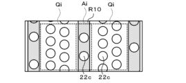
上面にウエハを載置可能なウエハ載置面を有し、電極を内蔵するセラミック基材と、
冷媒流路を有する冷却基材と、
前記セラミック基材と前記冷却基材とを接合する接合層と、
前記ウエハ載置面の基準面に、頂面でウエハの下面を支持する複数の小突起と、
を備えたウエハ載置台であって、
前記小突起の頂面は同一平面上にあり、
前記ウエハ載置面のうち平面視で前記冷媒流路と重複する流路重複範囲では、前記冷媒流路を平面視したときに前記ウエハ載置面と重複する範囲での最上流部に対向する部分において前記小突起の面積率が最低になっている、
ものである。
上面にウエハを載置可能なウエハ載置面を有し、電極を内蔵するセラミック基材と、
冷媒流路を有する冷却基材と、
前記セラミック基材と前記冷却基材とを接合する接合層と、
前記ウエハ載置面の基準面に、頂面でウエハの下面を支持する複数の小突起と、
を備えたウエハ載置台であって、
前記小突起の頂面は同一平面上にあり、
前記ウエハ載置面のうち平面視で前記冷媒流路と重複する流路重複範囲では、前記冷媒流路を平面視したときに前記ウエハ載置面と重複する範囲での最上流部に対向する部分において前記小突起の頂面から前記基準面までの距離が最長になっている、
ものである。
Claims (11)
- 上面にウエハを載置可能なウエハ載置面を有し、電極を内蔵するセラミック基材と、
冷媒流路を有する冷却基材と、
前記セラミック基材と前記冷却基材とを接合する接合層と、
前記ウエハ載置面の基準面に、頂面でウエハの下面を支持する複数の小突起と、
を備えたウエハ載置台であって、
前記小突起の頂面は同一平面上にあり、
前記ウエハ載置面のうち平面視で前記冷媒流路と重複する流路重複範囲では、前記冷媒流路を平面視したときに前記ウエハ載置面と重複する範囲での最上流部に対向する部分において前記小突起の面積率が最低になっている、ウエハ載置台。 - 前記流路重複範囲における前記小突起の面積率は、前記最上流部に対向する部分から前記冷媒流路の下流に行くにつれて徐々に高くなっている、
請求項1に記載のウエハ載置台。 - 前記流路重複範囲では、前記冷媒流路を平面視したときに前記ウエハ載置面と重複する範囲での最下流部に対向する部分における前記小突起の面積率は、前記最上流部に対向する部分における前記小突起の面積率の150%以上となっている、
請求項1又は2に記載のウエハ載置台。 - 前記流路重複範囲の所定の領域に比べて、前記所定の領域に隣接し前記流路重複範囲外の隣接領域の方が、前記小突起の面積率が高くなっている、
請求項1~3のいずれか1項に記載のウエハ載置台。 - 請求項1~4のいずれか1項に記載のウエハ載置台であって、
前記冷却基材を上下方向に貫通する穴
を備え、
前記冷媒流路は、前記穴の周辺領域では前記穴の周辺領域から外れた領域に比べて前記冷媒流路の断面積が小さくなっており、
前記ウエハ載置面のうち前記穴の直上領域から外れた周辺領域に比べて、前記直上領域の方が、前記小突起の面積率が高くなっている、ウエハ載置台。 - 上面にウエハを載置可能なウエハ載置面を有し、電極を内蔵するセラミック基材と、
冷媒流路を有する冷却基材と、
前記セラミック基材と前記冷却基材とを接合する接合層と、
前記ウエハ載置面の基準面に、頂面でウエハの下面を支持する複数の小突起と、
を備えたウエハ載置台であって、
前記小突起の頂面は同一平面上にあり、
前記ウエハ載置面のうち平面視で前記冷媒流路と重複する流路重複範囲では、前記冷媒流路を平面視したときに前記ウエハ載置面と重複する範囲での最上流部に対向する部分において前記小突起の頂面から前記基準面までの距離が最長になっている(ただし、前記小突起の頂面から前記基準面までの距離が全て同じものを除く)、ウエハ載置台。 - 前記流路重複範囲における前記小突起の頂面から前記基準面までの距離は、前記最上流部に対向する部分から前記冷媒流路の下流に行くにつれて徐々に短くなっている、
請求項6に記載のウエハ載置台。 - 前記流路重複範囲では、前記冷媒流路を平面視したときに前記ウエハ載置面と重複する範囲での最下流部に対向する部分における前記小突起の頂面から前記基準面までの距離は、前記最上流部に対向する部分における前記小突起の頂面から前記基準面までの距離の80%以下となっている、
請求項6又は7に記載のウエハ載置台。 - 前記流路重複範囲の所定の領域に比べて、前記所定の領域に隣接し前記流路重複範囲外の隣接領域の方が、前記小突起の頂面から前記基準面までの距離が短い、
請求項6~8のいずれか1項に記載のウエハ載置台。 - 請求項6~9のいずれか1項に記載のウエハ載置台であって、
前記冷却基材を上下方向に貫通する穴
を備え、
前記冷媒流路は、前記穴の周辺領域では前記穴の周辺領域から外れた領域に比べて前記冷媒流路の断面積が小さくなっており、
前記ウエハ載置面のうち前記穴の直上領域から外れた周辺領域に比べて、前記直上領域の方が、前記小突起の頂面から前記基準面までの距離が短くなっている、
ウエハ載置台。 - 前記冷却基材は、金属マトリックス複合材料で作製され、
前記接合層は、金属接合層である、
請求項1~10のいずれか1項に記載のウエハ載置台。
Priority Applications (5)
| Application Number | Priority Date | Filing Date | Title |
|---|---|---|---|
| JP2021192899A JP7572936B2 (ja) | 2021-11-29 | 2021-11-29 | ウエハ載置台 |
| CN202210852241.3A CN116190186A (zh) | 2021-11-29 | 2022-07-20 | 晶片载放台 |
| US17/931,916 US20230170191A1 (en) | 2021-11-29 | 2022-09-14 | Wafer placement table |
| KR1020220120678A KR20230080298A (ko) | 2021-11-29 | 2022-09-23 | 웨이퍼 배치대 |
| TW111145537A TWI841078B (zh) | 2021-11-29 | 2022-11-29 | 晶圓載置台 |
Applications Claiming Priority (1)
| Application Number | Priority Date | Filing Date | Title |
|---|---|---|---|
| JP2021192899A JP7572936B2 (ja) | 2021-11-29 | 2021-11-29 | ウエハ載置台 |
Publications (2)
| Publication Number | Publication Date |
|---|---|
| JP2023079422A JP2023079422A (ja) | 2023-06-08 |
| JP7572936B2 true JP7572936B2 (ja) | 2024-10-24 |
Family
ID=86449538
Family Applications (1)
| Application Number | Title | Priority Date | Filing Date |
|---|---|---|---|
| JP2021192899A Active JP7572936B2 (ja) | 2021-11-29 | 2021-11-29 | ウエハ載置台 |
Country Status (5)
| Country | Link |
|---|---|
| US (1) | US20230170191A1 (ja) |
| JP (1) | JP7572936B2 (ja) |
| KR (1) | KR20230080298A (ja) |
| CN (1) | CN116190186A (ja) |
| TW (1) | TWI841078B (ja) |
Families Citing this family (1)
| Publication number | Priority date | Publication date | Assignee | Title |
|---|---|---|---|---|
| WO2025191656A1 (ja) * | 2024-03-11 | 2025-09-18 | 日本碍子株式会社 | 半導体製造装置用部材の温度調整方法 |
Citations (5)
| Publication number | Priority date | Publication date | Assignee | Title |
|---|---|---|---|---|
| JP2002110774A (ja) | 2000-06-09 | 2002-04-12 | Applied Materials Inc | 全域温度制御静電チャック及びその製造方法 |
| JP2005191561A (ja) | 2003-12-05 | 2005-07-14 | Tokyo Electron Ltd | 静電チャック |
| JP2017208542A (ja) | 2016-05-13 | 2017-11-24 | Toto株式会社 | 静電チャック |
| JP2020004928A (ja) | 2018-07-02 | 2020-01-09 | 日本特殊陶業株式会社 | 静電チャック |
| JP2020161597A (ja) | 2019-03-26 | 2020-10-01 | 日本碍子株式会社 | ウエハ載置装置 |
Family Cites Families (6)
| Publication number | Priority date | Publication date | Assignee | Title |
|---|---|---|---|---|
| JPH0718438A (ja) * | 1993-06-17 | 1995-01-20 | Anelva Corp | 静電チャック装置 |
| JPH11330219A (ja) * | 1998-05-12 | 1999-11-30 | Hitachi Ltd | 静電吸着装置 |
| JP4409373B2 (ja) * | 2004-06-29 | 2010-02-03 | 日本碍子株式会社 | 基板載置装置及び基板温度調整方法 |
| JP6182082B2 (ja) | 2013-03-15 | 2017-08-16 | 日本碍子株式会社 | 緻密質複合材料、その製法及び半導体製造装置用部材 |
| JP6182084B2 (ja) | 2013-03-25 | 2017-08-16 | 日本碍子株式会社 | 緻密質複合材料、その製法、接合体及び半導体製造装置用部材 |
| US20180148835A1 (en) * | 2016-11-29 | 2018-05-31 | Lam Research Corporation | Substrate support with varying depths of areas between mesas and corresponding temperature dependent method of fabricating |
-
2021
- 2021-11-29 JP JP2021192899A patent/JP7572936B2/ja active Active
-
2022
- 2022-07-20 CN CN202210852241.3A patent/CN116190186A/zh active Pending
- 2022-09-14 US US17/931,916 patent/US20230170191A1/en not_active Abandoned
- 2022-09-23 KR KR1020220120678A patent/KR20230080298A/ko not_active Ceased
- 2022-11-29 TW TW111145537A patent/TWI841078B/zh active
Patent Citations (5)
| Publication number | Priority date | Publication date | Assignee | Title |
|---|---|---|---|---|
| JP2002110774A (ja) | 2000-06-09 | 2002-04-12 | Applied Materials Inc | 全域温度制御静電チャック及びその製造方法 |
| JP2005191561A (ja) | 2003-12-05 | 2005-07-14 | Tokyo Electron Ltd | 静電チャック |
| JP2017208542A (ja) | 2016-05-13 | 2017-11-24 | Toto株式会社 | 静電チャック |
| JP2020004928A (ja) | 2018-07-02 | 2020-01-09 | 日本特殊陶業株式会社 | 静電チャック |
| JP2020161597A (ja) | 2019-03-26 | 2020-10-01 | 日本碍子株式会社 | ウエハ載置装置 |
Also Published As
| Publication number | Publication date |
|---|---|
| KR20230080298A (ko) | 2023-06-07 |
| JP2023079422A (ja) | 2023-06-08 |
| TWI841078B (zh) | 2024-05-01 |
| US20230170191A1 (en) | 2023-06-01 |
| CN116190186A (zh) | 2023-05-30 |
| TW202322267A (zh) | 2023-06-01 |
Similar Documents
| Publication | Publication Date | Title |
|---|---|---|
| JP7645996B2 (ja) | ウエハ載置台 | |
| JP7514811B2 (ja) | ウエハ載置台 | |
| JP7580361B2 (ja) | ウエハ載置台 | |
| JP7364822B1 (ja) | ウエハ載置台 | |
| JP7583698B2 (ja) | ウエハ載置台 | |
| JP7572936B2 (ja) | ウエハ載置台 | |
| JP7714505B2 (ja) | ウエハ載置台及びそれを用いた半導体製造装置用部材 | |
| JP7522089B2 (ja) | ウエハ載置台 | |
| JP7496343B2 (ja) | ウエハ載置台 | |
| JP7686598B2 (ja) | ウエハ載置台 | |
| JP7620593B2 (ja) | ウエハ載置台 | |
| JP7606598B2 (ja) | ウエハ載置台 | |
| JP7621458B2 (ja) | ウエハ載置台 | |
| CN116564779A (zh) | 晶片载放台及采用了该晶片载放台的半导体制造装置用部件 |
Legal Events
| Date | Code | Title | Description |
|---|---|---|---|
| A621 | Written request for application examination |
Free format text: JAPANESE INTERMEDIATE CODE: A621 Effective date: 20230720 |
|
| A977 | Report on retrieval |
Free format text: JAPANESE INTERMEDIATE CODE: A971007 Effective date: 20240531 |
|
| A131 | Notification of reasons for refusal |
Free format text: JAPANESE INTERMEDIATE CODE: A131 Effective date: 20240604 |
|
| A521 | Request for written amendment filed |
Free format text: JAPANESE INTERMEDIATE CODE: A523 Effective date: 20240711 |
|
| TRDD | Decision of grant or rejection written | ||
| A01 | Written decision to grant a patent or to grant a registration (utility model) |
Free format text: JAPANESE INTERMEDIATE CODE: A01 Effective date: 20241008 |
|
| A61 | First payment of annual fees (during grant procedure) |
Free format text: JAPANESE INTERMEDIATE CODE: A61 Effective date: 20241011 |
|
| R150 | Certificate of patent or registration of utility model |
Ref document number: 7572936 Country of ref document: JP Free format text: JAPANESE INTERMEDIATE CODE: R150 |