WO2019049481A1 - 電気接続用ソケット - Google Patents
電気接続用ソケット Download PDFInfo
- Publication number
- WO2019049481A1 WO2019049481A1 PCT/JP2018/024820 JP2018024820W WO2019049481A1 WO 2019049481 A1 WO2019049481 A1 WO 2019049481A1 JP 2018024820 W JP2018024820 W JP 2018024820W WO 2019049481 A1 WO2019049481 A1 WO 2019049481A1
- Authority
- WO
- WIPO (PCT)
- Prior art keywords
- electrical connection
- socket
- circuit board
- pin
- communication hole
- Prior art date
- Legal status (The legal status is an assumption and is not a legal conclusion. Google has not performed a legal analysis and makes no representation as to the accuracy of the status listed.)
- Ceased
Links
Images

Classifications
-
- H—ELECTRICITY
- H01—ELECTRIC ELEMENTS
- H01R—ELECTRICALLY-CONDUCTIVE CONNECTIONS; STRUCTURAL ASSOCIATIONS OF A PLURALITY OF MUTUALLY-INSULATED ELECTRICAL CONNECTING ELEMENTS; COUPLING DEVICES; CURRENT COLLECTORS
- H01R12/00—Structural associations of a plurality of mutually-insulated electrical connecting elements, specially adapted for printed circuits, e.g. printed circuit boards [PCB], flat or ribbon cables, or like generally planar structures, e.g. terminal strips, terminal blocks; Coupling devices specially adapted for printed circuits, flat or ribbon cables, or like generally planar structures; Terminals specially adapted for contact with, or insertion into, printed circuits, flat or ribbon cables, or like generally planar structures
- H01R12/70—Coupling devices
- H01R12/71—Coupling devices for rigid printing circuits or like structures
- H01R12/712—Coupling devices for rigid printing circuits or like structures co-operating with the surface of the printed circuit or with a coupling device exclusively provided on the surface of the printed circuit
- H01R12/716—Coupling device provided on the PCB
- H01R12/718—Contact members provided on the PCB without an insulating housing
-
- G—PHYSICS
- G01—MEASURING; TESTING
- G01R—MEASURING ELECTRIC VARIABLES; MEASURING MAGNETIC VARIABLES
- G01R1/00—Details of instruments or arrangements of the types included in groups G01R5/00 - G01R13/00 and G01R31/00
- G01R1/02—General constructional details
- G01R1/06—Measuring leads; Measuring probes
- G01R1/067—Measuring probes
- G01R1/06711—Probe needles; Cantilever beams; "Bump" contacts; Replaceable probe pins
- G01R1/06716—Elastic
- G01R1/06722—Spring-loaded
-
- G—PHYSICS
- G01—MEASURING; TESTING
- G01R—MEASURING ELECTRIC VARIABLES; MEASURING MAGNETIC VARIABLES
- G01R1/00—Details of instruments or arrangements of the types included in groups G01R5/00 - G01R13/00 and G01R31/00
- G01R1/02—General constructional details
- G01R1/06—Measuring leads; Measuring probes
- G01R1/067—Measuring probes
- G01R1/073—Multiple probes
- G01R1/07307—Multiple probes with individual probe elements, e.g. needles, cantilever beams or bump contacts, fixed in relation to each other, e.g. bed of nails fixture or probe card
- G01R1/07314—Multiple probes with individual probe elements, e.g. needles, cantilever beams or bump contacts, fixed in relation to each other, e.g. bed of nails fixture or probe card the body of the probe being perpendicular to test object, e.g. bed of nails or probe with bump contacts on a rigid support
-
- H—ELECTRICITY
- H01—ELECTRIC ELEMENTS
- H01R—ELECTRICALLY-CONDUCTIVE CONNECTIONS; STRUCTURAL ASSOCIATIONS OF A PLURALITY OF MUTUALLY-INSULATED ELECTRICAL CONNECTING ELEMENTS; COUPLING DEVICES; CURRENT COLLECTORS
- H01R12/00—Structural associations of a plurality of mutually-insulated electrical connecting elements, specially adapted for printed circuits, e.g. printed circuit boards [PCB], flat or ribbon cables, or like generally planar structures, e.g. terminal strips, terminal blocks; Coupling devices specially adapted for printed circuits, flat or ribbon cables, or like generally planar structures; Terminals specially adapted for contact with, or insertion into, printed circuits, flat or ribbon cables, or like generally planar structures
- H01R12/50—Fixed connections
- H01R12/51—Fixed connections for rigid printed circuits or like structures
- H01R12/55—Fixed connections for rigid printed circuits or like structures characterised by the terminals
- H01R12/57—Fixed connections for rigid printed circuits or like structures characterised by the terminals surface mounting terminals
-
- H—ELECTRICITY
- H01—ELECTRIC ELEMENTS
- H01R—ELECTRICALLY-CONDUCTIVE CONNECTIONS; STRUCTURAL ASSOCIATIONS OF A PLURALITY OF MUTUALLY-INSULATED ELECTRICAL CONNECTING ELEMENTS; COUPLING DEVICES; CURRENT COLLECTORS
- H01R12/00—Structural associations of a plurality of mutually-insulated electrical connecting elements, specially adapted for printed circuits, e.g. printed circuit boards [PCB], flat or ribbon cables, or like generally planar structures, e.g. terminal strips, terminal blocks; Coupling devices specially adapted for printed circuits, flat or ribbon cables, or like generally planar structures; Terminals specially adapted for contact with, or insertion into, printed circuits, flat or ribbon cables, or like generally planar structures
- H01R12/50—Fixed connections
- H01R12/51—Fixed connections for rigid printed circuits or like structures
- H01R12/55—Fixed connections for rigid printed circuits or like structures characterised by the terminals
- H01R12/58—Fixed connections for rigid printed circuits or like structures characterised by the terminals terminals for insertion into holes
-
- H—ELECTRICITY
- H01—ELECTRIC ELEMENTS
- H01R—ELECTRICALLY-CONDUCTIVE CONNECTIONS; STRUCTURAL ASSOCIATIONS OF A PLURALITY OF MUTUALLY-INSULATED ELECTRICAL CONNECTING ELEMENTS; COUPLING DEVICES; CURRENT COLLECTORS
- H01R12/00—Structural associations of a plurality of mutually-insulated electrical connecting elements, specially adapted for printed circuits, e.g. printed circuit boards [PCB], flat or ribbon cables, or like generally planar structures, e.g. terminal strips, terminal blocks; Coupling devices specially adapted for printed circuits, flat or ribbon cables, or like generally planar structures; Terminals specially adapted for contact with, or insertion into, printed circuits, flat or ribbon cables, or like generally planar structures
- H01R12/70—Coupling devices
- H01R12/71—Coupling devices for rigid printing circuits or like structures
- H01R12/712—Coupling devices for rigid printing circuits or like structures co-operating with the surface of the printed circuit or with a coupling device exclusively provided on the surface of the printed circuit
- H01R12/714—Coupling devices for rigid printing circuits or like structures co-operating with the surface of the printed circuit or with a coupling device exclusively provided on the surface of the printed circuit with contacts abutting directly the printed circuit; Button contacts therefore provided on the printed circuit
-
- H—ELECTRICITY
- H01—ELECTRIC ELEMENTS
- H01R—ELECTRICALLY-CONDUCTIVE CONNECTIONS; STRUCTURAL ASSOCIATIONS OF A PLURALITY OF MUTUALLY-INSULATED ELECTRICAL CONNECTING ELEMENTS; COUPLING DEVICES; CURRENT COLLECTORS
- H01R13/00—Details of coupling devices of the kinds covered by groups H01R12/70 or H01R24/00 - H01R33/00
- H01R13/02—Contact members
- H01R13/193—Means for increasing contact pressure at the end of engagement of coupling part, e.g. zero insertion force or no friction
-
- H—ELECTRICITY
- H01—ELECTRIC ELEMENTS
- H01R—ELECTRICALLY-CONDUCTIVE CONNECTIONS; STRUCTURAL ASSOCIATIONS OF A PLURALITY OF MUTUALLY-INSULATED ELECTRICAL CONNECTING ELEMENTS; COUPLING DEVICES; CURRENT COLLECTORS
- H01R13/00—Details of coupling devices of the kinds covered by groups H01R12/70 or H01R24/00 - H01R33/00
- H01R13/646—Details of coupling devices of the kinds covered by groups H01R12/70 or H01R24/00 - H01R33/00 specially adapted for high-frequency, e.g. structures providing an impedance match or phase match
- H01R13/6473—Impedance matching
-
- H—ELECTRICITY
- H01—ELECTRIC ELEMENTS
- H01R—ELECTRICALLY-CONDUCTIVE CONNECTIONS; STRUCTURAL ASSOCIATIONS OF A PLURALITY OF MUTUALLY-INSULATED ELECTRICAL CONNECTING ELEMENTS; COUPLING DEVICES; CURRENT COLLECTORS
- H01R13/00—Details of coupling devices of the kinds covered by groups H01R12/70 or H01R24/00 - H01R33/00
- H01R13/648—Protective earth or shield arrangements on coupling devices, e.g. anti-static shielding
- H01R13/658—High frequency shielding arrangements, e.g. against EMI [Electro-Magnetic Interference] or EMP [Electro-Magnetic Pulse]
- H01R13/6591—Specific features or arrangements of connection of shield to conductive members
- H01R13/6594—Specific features or arrangements of connection of shield to conductive members the shield being mounted on a PCB and connected to conductive members
-
- H—ELECTRICITY
- H01—ELECTRIC ELEMENTS
- H01R—ELECTRICALLY-CONDUCTIVE CONNECTIONS; STRUCTURAL ASSOCIATIONS OF A PLURALITY OF MUTUALLY-INSULATED ELECTRICAL CONNECTING ELEMENTS; COUPLING DEVICES; CURRENT COLLECTORS
- H01R12/00—Structural associations of a plurality of mutually-insulated electrical connecting elements, specially adapted for printed circuits, e.g. printed circuit boards [PCB], flat or ribbon cables, or like generally planar structures, e.g. terminal strips, terminal blocks; Coupling devices specially adapted for printed circuits, flat or ribbon cables, or like generally planar structures; Terminals specially adapted for contact with, or insertion into, printed circuits, flat or ribbon cables, or like generally planar structures
- H01R12/50—Fixed connections
- H01R12/51—Fixed connections for rigid printed circuits or like structures
- H01R12/55—Fixed connections for rigid printed circuits or like structures characterised by the terminals
-
- H—ELECTRICITY
- H01—ELECTRIC ELEMENTS
- H01R—ELECTRICALLY-CONDUCTIVE CONNECTIONS; STRUCTURAL ASSOCIATIONS OF A PLURALITY OF MUTUALLY-INSULATED ELECTRICAL CONNECTING ELEMENTS; COUPLING DEVICES; CURRENT COLLECTORS
- H01R12/00—Structural associations of a plurality of mutually-insulated electrical connecting elements, specially adapted for printed circuits, e.g. printed circuit boards [PCB], flat or ribbon cables, or like generally planar structures, e.g. terminal strips, terminal blocks; Coupling devices specially adapted for printed circuits, flat or ribbon cables, or like generally planar structures; Terminals specially adapted for contact with, or insertion into, printed circuits, flat or ribbon cables, or like generally planar structures
- H01R12/70—Coupling devices
- H01R12/71—Coupling devices for rigid printing circuits or like structures
-
- H—ELECTRICITY
- H01—ELECTRIC ELEMENTS
- H01R—ELECTRICALLY-CONDUCTIVE CONNECTIONS; STRUCTURAL ASSOCIATIONS OF A PLURALITY OF MUTUALLY-INSULATED ELECTRICAL CONNECTING ELEMENTS; COUPLING DEVICES; CURRENT COLLECTORS
- H01R12/00—Structural associations of a plurality of mutually-insulated electrical connecting elements, specially adapted for printed circuits, e.g. printed circuit boards [PCB], flat or ribbon cables, or like generally planar structures, e.g. terminal strips, terminal blocks; Coupling devices specially adapted for printed circuits, flat or ribbon cables, or like generally planar structures; Terminals specially adapted for contact with, or insertion into, printed circuits, flat or ribbon cables, or like generally planar structures
- H01R12/70—Coupling devices
- H01R12/71—Coupling devices for rigid printing circuits or like structures
- H01R12/712—Coupling devices for rigid printing circuits or like structures co-operating with the surface of the printed circuit or with a coupling device exclusively provided on the surface of the printed circuit
-
- H—ELECTRICITY
- H01—ELECTRIC ELEMENTS
- H01R—ELECTRICALLY-CONDUCTIVE CONNECTIONS; STRUCTURAL ASSOCIATIONS OF A PLURALITY OF MUTUALLY-INSULATED ELECTRICAL CONNECTING ELEMENTS; COUPLING DEVICES; CURRENT COLLECTORS
- H01R12/00—Structural associations of a plurality of mutually-insulated electrical connecting elements, specially adapted for printed circuits, e.g. printed circuit boards [PCB], flat or ribbon cables, or like generally planar structures, e.g. terminal strips, terminal blocks; Coupling devices specially adapted for printed circuits, flat or ribbon cables, or like generally planar structures; Terminals specially adapted for contact with, or insertion into, printed circuits, flat or ribbon cables, or like generally planar structures
- H01R12/70—Coupling devices
- H01R12/71—Coupling devices for rigid printing circuits or like structures
- H01R12/712—Coupling devices for rigid printing circuits or like structures co-operating with the surface of the printed circuit or with a coupling device exclusively provided on the surface of the printed circuit
- H01R12/716—Coupling device provided on the PCB
-
- H—ELECTRICITY
- H01—ELECTRIC ELEMENTS
- H01R—ELECTRICALLY-CONDUCTIVE CONNECTIONS; STRUCTURAL ASSOCIATIONS OF A PLURALITY OF MUTUALLY-INSULATED ELECTRICAL CONNECTING ELEMENTS; COUPLING DEVICES; CURRENT COLLECTORS
- H01R12/00—Structural associations of a plurality of mutually-insulated electrical connecting elements, specially adapted for printed circuits, e.g. printed circuit boards [PCB], flat or ribbon cables, or like generally planar structures, e.g. terminal strips, terminal blocks; Coupling devices specially adapted for printed circuits, flat or ribbon cables, or like generally planar structures; Terminals specially adapted for contact with, or insertion into, printed circuits, flat or ribbon cables, or like generally planar structures
- H01R12/70—Coupling devices
- H01R12/71—Coupling devices for rigid printing circuits or like structures
- H01R12/72—Coupling devices for rigid printing circuits or like structures coupling with the edge of the rigid printed circuits or like structures
- H01R12/73—Coupling devices for rigid printing circuits or like structures coupling with the edge of the rigid printed circuits or like structures connecting to other rigid printed circuits or like structures
-
- H—ELECTRICITY
- H01—ELECTRIC ELEMENTS
- H01R—ELECTRICALLY-CONDUCTIVE CONNECTIONS; STRUCTURAL ASSOCIATIONS OF A PLURALITY OF MUTUALLY-INSULATED ELECTRICAL CONNECTING ELEMENTS; COUPLING DEVICES; CURRENT COLLECTORS
- H01R24/00—Two-part coupling devices, or either of their cooperating parts, characterised by their overall structure
- H01R24/38—Two-part coupling devices, or either of their cooperating parts, characterised by their overall structure having concentrically or coaxially arranged contacts
- H01R24/40—Two-part coupling devices, or either of their cooperating parts, characterised by their overall structure having concentrically or coaxially arranged contacts specially adapted for high frequency
Definitions
- the present disclosure relates to electrical connection sockets.
- a grounded metal case is used to suppress signal deterioration.
- a signal pin for transmitting a signal is disposed in a communication hole provided to connect the upper surface and the lower surface of the metal casing, and the signal pin is an inner wall surface of the communication hole. Between the two, and so as to constitute a coaxial line.
- the socket for electrical connection using the metal housing is more susceptible to the crosstalk between the metal housing and the circuit board than the socket for resin electrical connection according to the prior art. Due to the crosstalk, the signal transmission capability may be reduced regardless of the connection state of the signal pin itself. Typically, the ground voltage of the metal housing becomes unstable due to the crosstalk. As a result, the characteristic impedance of the signal path formed in the signal pin becomes unstable, which may cause signal degradation due to the reflection in the signal path.
- This indication is made in view of the above-mentioned problem, and makes it a subject to provide a socket for electric connection which can control crosstalk between a metal case and a circuit board.
- a socket for electrical connection that relays transmission and reception of electrical signals between a circuit board and an electrical component, comprising: A metal case having a communication hole communicating between the upper surface and the lower surface of the metal case, the electric component mounted on the upper surface side, and the circuit board disposed on the lower surface side;
- the through hole is inserted into the through hole so as to form a coaxial line between the through hole and the inner wall surface of the through hole, one end is electrically connected to the pad electrode for the signal path of the circuit board, and the other end is a signal of the electric component Signal pins electrically connected to the terminals for the Equipped with
- the metal housing is an electrical connection socket disposed on the circuit board such that an air gap is formed between the lower surface of the metal housing and the upper surface of the circuit board.
- FIG. 1 is a side cross-sectional view of the electrical connection socket 1 according to the present embodiment.
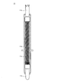
- FIG. 2 is a side sectional view of the signal pin 11 of the electrical connection socket 1 according to the present embodiment.
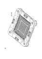
- FIG. 3 is a perspective view of the metal casing 10 of the electrical connection socket 1 according to the present embodiment as viewed from the top side.
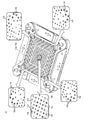
- FIG. 4 is a perspective view of the metal casing 10 of the electrical connection socket 1 according to the present embodiment as viewed from the lower surface side.
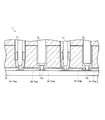
- FIG. 5 is a view showing an air gap formed on the lower surface side of the metal casing 10 in the electrical connection socket 1 according to the present embodiment.
- the electrical connection socket 1 is a surface mount type socket, and is mounted on the circuit board P. Then, the IC package B is mounted on the top of the electrical connection socket 1.
- the circuit board P side as viewed from the electrical connection socket 1 is described as being on the lower side (corresponding to the lower side in FIG. 1) and the IC package B side as the upper side (corresponding to the upper side in .
- the electrical connection socket 1 is applied to, for example, an application for performing a performance test of the IC package B.
- the electrical connection socket 1 electrically connects the IC package B disposed on the upper surface side of itself and the circuit board P on the IC test apparatus side disposed on the lower surface side of itself.
- the most efficient way to maintain the data transfer rate is to solder the IC package B directly to the circuit board P. In this case, however, the circuit board P and the IC package B can be made detachable. , And electrical connection using the socket 1 for electrical connection.
- the IC package B is, for example, an IC package of BGA (Ball Grid Array) type.
- the IC package B is, for example, as a terminal for external connection, a first solder ball Ba (first terminal) for a signal path projecting downward from the lower surface of the package body, and a second solder ball Bb for ground connection. A second terminal).
- the IC package B is mounted on the electrical connection socket 1 by a latch (not shown) provided on the electrical connection socket 1.
- a latch (not shown) provided on the electrical connection socket 1.
- the IC package B is mounted on the electrical connection socket 1 so that the upper surface of the IC package B is pressed, and the IC package B is removed from the electrical connection socket 1 by opening the latch. It is supposed to be.
- the circuit board P is, for example, a printed circuit board (PCB) board.
- PCB printed circuit board
- a signal for performing a performance test of the IC package B a circuit pattern for a signal path for receiving and processing a signal from the IC package B, and a ground voltage are supplied.
- a ground pattern etc. is formed.
- the electrical connection socket 1 is attached to the circuit board P by a bolt, a nut or the like.
- the electrical connection socket 1 includes a metal casing 10, a signal pin 11 for transmitting a signal between the circuit board P and the IC package B, and a ground pin for supplying a ground voltage from the circuit board P to the IC package B. It has 12 mag.
- the metal housing 10 is formed of, for example, a metal member such as aluminum or copper.
- the metal casing 10 is, for example, formed entirely of aluminum and has conductivity, and the ground voltage secured by the protrusion 10 t (details will be described later) of the lower surface of the metal casing 10 is the metal casing. Supplied throughout the body 10.
- the metal casing 10 is configured by connecting an upper plate and a lower plate using a fixing member (for example, a bolt and a nut).
- a fixing member for example, a bolt and a nut
- the metal casing 10 may be integrally configured by one member, or may be configured by joining a plurality of plates.
- the metal casing 10 may be made of a partially insulating material.
- the metal housing 10 has a first communication hole 10a through which the signal pin 11 is inserted, and a second communication hole 10b through which the ground pin 12 is inserted.
- Each of the first communication hole 10 a and the second communication hole 10 b is formed so as to communicate from the upper surface to the lower surface of the metal housing 10.
- the first communication holes 10a and the second communication holes 10b have, for example, a circular shape in plan view.
- the inner wall surface of the first communication hole 10a of the metal housing 10, a part of the lower surface of the metal housing 10, and the upper surface of the metal housing 10 form an anodic oxidation region 10s.
- the signal pin 11 is disposed in the first communication hole 10a so as to be separated from the inner wall surface of the first communication hole 10a. That is, the signal pin 11 is disposed in the first communication hole 10a in a state of being electrically insulated from the metal housing 10, and forms a coaxial line with the inner wall surface of the first communication hole 10a. .
- the distance between the outer peripheral surface of the signal pin 11 (pin barrel 11a) and the inner wall surface of the first communication hole 10a is a predetermined value (for example, 50 ⁇ ) at each position of the characteristic impedance of the coaxial line formed by the signal pin 11. It is adjusted to become).
- the signal pin 11 provides an impedance-matched signal path between the IC package B and the circuit board P with such a configuration.
- the signal pin 11 includes a pin barrel 11a, a first plunger 11b, a second plunger 11c, and a spring 11d (see FIG. 2).
- the pin barrel 11a is a cylindrical member, and is disposed so as to extend in the vertical direction along the first communication hole 10a in the first communication hole 10a.
- the pin barrel 11a is fixed in the first communication hole 10a in a state of being separated from the inner wall surface of the first communication hole 10a by, for example, insulating holding members 13a and 13b.
- the holding member 13a has an annular shape, and is press-fitted and fixed to the first communication hole 10a on the upper side of the first communication hole 10a.
- the holding member 13b has an annular shape, is press-fitted and fixed to the lower side of the pin barrel 11a, and is locked to the first communication hole 10a. And the pin barrel 11a is being fixed so that it may be clamped from the upper and lower sides in the 1st communicating hole 10a via the said holding members 13a and 13b.
- the first plunger 11b is connected to the upper end of the pin barrel 11a in a state where it can slide in the vertical direction.
- the lower end of the first plunger 11b is connected to the upper end of the spring 11d disposed in the pin barrel 11a, and the upper end is configured to project upward from the opening formed in the upper end of the pin barrel 11a. .
- the upper end portion of the first plunger 11 b protrudes above the upper surface of the metal housing 10.
- the second plunger 11c is connected to the lower end portion of the pin barrel 11a so as to be vertically slidable.
- the second plunger 11c is configured such that the upper end is connected to the lower end of the spring 11d disposed in the pin barrel 11a, and the lower end protrudes downward from the opening formed in the lower end of the pin barrel 11a. . Further, the lower end portion of the second plunger 11 c protrudes below the lower surface of the metal housing 10.
- the spring 11d is disposed between the first plunger 11b and the second plunger 11c in the pin barrel 11a to bias the first plunger 11b upward and bias the second plunger 11c downward.
- the contact pressure between the upper end of the first plunger 11b and the first solder ball Ba of the IC package B and the contact pressure between the lower end of the second plunger 11c and the first pad electrode Pa of the circuit board P are secured.
- the spring 11d is configured to be in contact with the inner wall surface of the pin barrel 11a, and conducts between the first plunger 11b, the pin barrel 11a, and the second plunger 11c.
- the pin barrel 11a, the first plunger 11b, the second plunger 11c, and the spring 11d are each formed of a metal member. However, as described above, these members are disposed in a state of being electrically insulated from the inner wall surface of the first communication hole 10a.
- the upper end portion of the first plunger 11b is in contact with the first solder ball Ba of the IC package B, and the lower end portion of the second plunger 11c is in contact with the first pad electrode Pa of the circuit board P.
- the signal transmission between the IC package B and the circuit board P is relayed.
- the ground pin 12 (pin barrel 12a) is disposed in the second communication hole 10b so as to be in contact with the inner wall surface of the second communication hole 10b. That is, the ground pin 12 is disposed in the second communication hole 10 b in a state of being electrically connected to the metal housing 10 on the inner wall surface of the second communication hole 10 b.
- the ground pin 12 is more preferably arranged to be electrically connected to the second communication hole 10b in the upper region of the second communication hole 10b.
- the ground pin 12 includes a pin barrel 12a, a first plunger 12b, a second plunger 12c, and a spring (not shown).
- the ground pin 12 is configured substantially the same as the signal pin 11. That is, when the IC package B is attached to the electrical connection socket 1, the upper end portion of the first plunger 12b contacts the second solder ball Bb for ground of the IC package B, and the lower end of the second plunger 12c. The portion is in contact with the second pad electrode Pb for ground formed on the circuit board P. Thus, the ground voltage of the circuit board P is supplied to the ground pattern of the IC package B through the ground pin 12.
- the ground pin 12 is disposed in contact with the inner wall surface of the second communication hole 10 b of the metal housing 10.
- the electrical connection socket 1 may further be provided with a power pin for supplying operating power from the circuit board P to the IC package B.
- the electrical connection socket 1 according to this embodiment is formed from the lower surface of the metal casing 10 so that an air gap (see FIG. 5) is formed between the lower surface of the metal casing 10 and the upper surface of the circuit board P. And a plurality of projections 10t projecting toward the That is, the electrical connection socket 1 according to the present embodiment uses the air gap to reduce crosstalk between the signal path formed on the circuit board P and the metal casing 10.
- the plurality of protrusions 10t are typically formed in a ring shape on the lower surface of the metal housing 10 so as to surround the plurality of second communication holes 10b (see FIG. 4).
- the plurality of projections 10t are disposed, for example, in the four corner areas of the lower surface of the metal housing 10 and in the central area of the lower surface of the metal housing 10 so as to support the metal housing 10 from below. There is.
- the protrusion height of the projection part 10t it is desirable to set so that the air gap between the lower surface of the metal housing 10 and the upper surface of the circuit board P may be 0.1 mm or more, for example.
- the area in which the protrusion 10t is disposed is a region where the lower surface of the metal casing 10 and the upper surface of the circuit board P face each other even in consideration of the necessity of grounding the metal casing 10 by the protrusion 10t.
- 95% or more of the above is set to be the air gap region.
- the protrusion 10 t also has a function of electrically connecting the metal housing 10 directly to the second pad electrode Pb for ground of the circuit board P. Similar to the metal housing 10, the protrusion 10t is made of a metal member (for example, an aluminum material). The projection 10t is in a state where the metal member is exposed without the surface being anodized.
- the lower end portion of the protrusion 10 t contacts the second pad electrode Pb in the outer peripheral region of the region where the ground pin 12 contacts the second pad electrode Pb of the circuit board P.
- the protrusion 10 t grounds the metal casing 10.
- the socket for electrical connection 1 ground-connects the metal casing 10 by the projection 10t.
- the grounding of the metal casing 10 is made between the outer peripheral surface of the ground pin 12 and the inner wall surface of the communication hole of the metal casing 10 (for example, the first communication hole 10a in FIG. 1). It is carried out by contact, and is carried out via the impedance due to the contact resistance between the outer peripheral surface of the ground pin 12 and the inner wall surface of the communication hole.
- the metal housing 10 is connected to the ground without the impedance due to the contact resistance between the outer peripheral surface of the ground pin 12 and the inner wall surface of the first communication hole 10a. It means that you can do it.
- the supply of the ground voltage from the protrusion 10 t is also performed to the ground pin 12 through the contact portion between the inner wall surface of the second communication hole 10 b and the ground pin 12.
- the ground pin 12 is disposed in the lower region of the second communication hole 10b so as to be separated from the inner wall surface of the second communication hole 10b, and in the upper region of the second communication hole 10b It is arrange
- an aspect is shown in which an air gap is formed between the lower surface of the metal housing 10 and the upper surface of the circuit board P by the protrusion 10 t.
- the configuration for forming the air gap may be another method.
- the socket for electrical connection 1 is a circuit board so that the entire lower surface of the metal casing 10 is separated from the upper surface of the circuit board P. It may be mounted on P.
- the electrical connection socket 1 is mounted on the circuit board P.
- the protrusion 10 t provided on the lower surface of the metal casing 10 contacts the second pad electrode Pb for ground of the circuit board P.
- the metal housing 10 is electrically connected directly to the second pad electrode Pb for ground of the circuit board P, and a stable ground voltage is secured.
- the IC package B is mounted on the electrical connection socket 1. Thereafter, when the upper surface of the IC package B is pressed downward using a latch provided in the electrical connection socket 1, the first and second solder balls Ba and Bb of the IC package B are signal pins 11 and ground pins. Abuts on each of the first plungers 11b and 12b. Thereby, the electrical contact between the first solder ball Ba for signal path and the first plunger portion 11 b of the signal pin 11, and the second solder ball Bb for ground and the first plunger portion 12 b of the ground pin 12. Electrical contact will be secured.
- the second plunger 11 c of the signal pin 11 and the second plunger 12 c of the ground pin 12 are for the first pad electrode Pa for signal path on the circuit board P and for ground, respectively.
- Contact with the second pad electrode Pb As a result, electrical contact between the first pad electrode Pa for signal path and the second plunger 11 c of the signal pin 11, and between the second pad electrode Pb for grounding and the second plunger 12 c of the grounding pin 12. Electrical contact will be secured.
- the biasing force of the spring 11d acts on the first plunger portion 11b and the second plunger portion 11c of the signal pin 11 in the direction away from each other along the vertical direction.
- the biasing force of a spring acts on the first plunger portion 12b and the second plunger portion 12c of the ground pin 12 in the direction away from each other along the vertical direction.
- the IC package B and the circuit board P are electrically connected to each other through the electrical connection socket 1, whereby the performance test of the IC package B and the like are performed.
- the ground voltage of the metal housing 10 is held in a stable state, whereby signal transmission via the signal pin 11 is performed in a state in which signal deterioration is suppressed.
- the metal casing 10 is the circuit board P so that an air gap is formed between the lower surface of the metal casing 10 and the upper surface of the circuit board P Arranged on top. Therefore, according to the socket 1 for electrical connection which concerns on this embodiment, the crosstalk between the metal housing 10 and the circuit board P can be suppressed. By this, it is possible to suppress the destabilization of the ground potential of the metal housing 10 and to suppress the signal deterioration at the time of signal transmission.
- the electrical connection socket 1 has a plurality of protruding portions 10t disposed so as to project downward from the lower surface of the metal housing 10 and to be in contact with the upper surface of the circuit board P.
- the air gap is formed in a region between the plurality of protrusions 10t.
- the mode of holding the signal pin 11 so as to be separated from the inner wall surface of the first communication hole 10a is shown.
- the signal pin 11 may be electrically insulated from the metal housing 10, and an insulating member may be interposed between the signal pin 11 and the inner wall surface of the first communication hole 10a.
- the pin barrel 11a of the signal pin 11 is not necessarily fixed, and the pin barrel 11a may be configured to be slidable in the first communication hole 10a.
- the aspect which has the ground pin 12 was shown as an example of a structure of the socket 1 for electrical connections.
- the ground pin 12 may not be provided in the electrical connection socket 1 in consideration of grounding of the metal housing 10 being performed by the protrusion 10 t.
- IC package B was shown as an example of the electrical component B connected to the upper part side of the socket 1 for electrical connections.
- the electrical component B connected to the upper side of the electrical connection socket 1 may be a coaxial cable or the like.
- the aspect used for the test of IC package B was shown as an example of the application of the socket 1 for electrical connections.
- the application of the socket 1 for electrical connection can be applied to any application for electrical connection other than the test of the IC package B.
- the ground voltage of the metal housing can be stabilized, and signal deterioration at the time of signal transmission can be suppressed.
Landscapes
- Physics & Mathematics (AREA)
- General Physics & Mathematics (AREA)
- Connecting Device With Holders (AREA)
- Measuring Leads Or Probes (AREA)
Abstract
Description
回路基板と電気部品との間における電気信号の授受を中継する電気接続用ソケットであって、
自身の上面と下面との間を連通する連通孔を有し、前記上面側に前記電気部品が装着され、且つ前記下面側に前記回路基板が配設される金属筐体と、
前記連通孔の内壁面との間で同軸線路を構成するように前記連通孔内に挿通され、一端が前記回路基板の信号路用のパッド電極と電気接続し、他端が前記電気部品の信号路用の端子と電気接続するシグナルピンと、
を備え、
前記金属筐体は、自身の前記下面と前記回路基板の上面との間にエアギャップが形成されるように、前記回路基板上に配設される
電気接続用ソケットである。
以下、図1~図5を参照して、一実施形態に係る電気接続用ソケットの構成の一例について説明する。
本実施形態に係る電気接続用ソケット1は、金属筐体10の下面と回路基板Pの上面の間にエアギャップ(図5を参照)が形成されるように、金属筐体10の下面から下方に向かって突出する複数の突起部10tを有している。つまり、本実施形態に係る電気接続用ソケット1は、当該エアギャップを利用して、回路基板P上に形成された信号路と金属筐体10と間におけるクロストークを低減する。
次に、本実施形態に係る電気接続用ソケット1の使用態様について、説明する。
以上のように、本実施形態に係る電気接続用ソケット1は、金属筐体10の下面と回路基板Pの上面との間にエアギャップが形成されるように、金属筐体10が回路基板P上に配設される。従って、本実施形態に係る電気接続用ソケット1によれば、金属筐体10と回路基板Pとの間におけるクロストークを抑制することができる。これによって、金属筐体10のグラウンド電位の不安定化を抑制し、信号伝達時の信号劣化を抑制することが可能である。
本発明は、上記実施形態に限らず、種々に変形態様が考えられる。
10 金属筐体
10a 第1連通孔
10b 第2連通孔
10s 陽極酸化領域
10t 突起部
11 シグナルピン
11a ピンバレル
11b 第1プランジャ
11c 第2プランジャ
11d スプリング
12 グラウンドピン
12a ピンバレル
12b 第1プランジャ
12c 第2プランジャ
13a、13b 保持部材
B ICパッケージ
Ba 第1半田ボール
Bb 第2半田ボール
P 回路基板
Pa 第1パッド電極
Pb 第2パッド電極
Claims (11)
- 回路基板と電気部品との間における電気信号の授受を中継する電気接続用ソケットであって、
自身の上面と下面との間を連通する連通孔を有し、前記上面側に前記電気部品が装着され、且つ前記下面側に前記回路基板が配設される金属筐体と、
前記連通孔の内壁面との間で同軸線路を構成するように前記連通孔内に挿通され、一端が前記回路基板の信号路用のパッド電極と電気接続し、他端が前記電気部品の信号路用の端子と電気接続するシグナルピンと、
を備え、
前記金属筐体は、自身の前記下面と前記回路基板の上面との間にエアギャップが形成されるように、前記回路基板上に配設される
電気接続用ソケット。 - 前記金属筐体は、前記下面から下方に向かって突出して、前記回路基板の上面と接触するように配設された複数の突起部を有し、
前記エアギャップは、複数の前記突起部の間の領域に形成される
請求項1に記載の電気接続用ソケット。 - 前記突起部は、前記エアギャップの高さが0.1mm以上となるように、前記金属筐体の前記下面から下方に向かって突出する
請求項2に記載の電気接続用ソケット。 - 前記金属筐体の前記下面と前記回路基板の上面とが対向する領域のうち95%以上が前記エアギャップ領域である
請求項2に記載の電気接続用ソケット。 - 前記突起部は、少なくとも前記金属筐体の前記下面の四隅の領域に配設されている
請求項2に記載の電気接続用ソケット。 - 前記金属筐体の前記上面と前記下面との間を連通する第2連通孔内に挿通され、一端が前記回路基板に形成されたグラウンド用の第2パッド電極と電気接続し、他端が前記電気部品のグラウンド用の第2端子と電気接続するグラウンドピン、を更に有する
請求項2に記載の電気接続用ソケット。 - 前記突起部は、前記回路基板上に形成されたグラウンド用の前記第2パッド電極と接触して、前記金属筐体を接地するように配設される
請求項6に記載の電気接続用ソケット。 - 前記突起部は、前記金属筐体の前記下面において、前記第2連通孔の縁部を囲繞する形状を呈する
請求項7に記載の電気接続用ソケット。 - 前記シグナルピンは、自身の外周面と前記連通孔の内壁面との間が離間するように、前記連通孔内に挿通されている
請求項1に記載の電気接続用ソケット。 - 前記シグナルピンは、前記連通孔内に固定されたピンバレルと、当該ピンバレルの上端部及び下端部それぞれにおいて当該ピンバレルに対して上下方向に摺動可能に、当該ピンバレルに連結された第1及び第2プランジャと、を含んで構成される
請求項1に記載の電気接続用ソケット。 - 前記電気部品は、ICパッケージである
請求項1に記載の電気接続用ソケット。
Priority Applications (4)
| Application Number | Priority Date | Filing Date | Title |
|---|---|---|---|
| CN201880057903.XA CN111213061B (zh) | 2017-09-08 | 2018-06-29 | 电连接用插座 |
| SG11202002099QA SG11202002099QA (en) | 2017-09-08 | 2018-06-29 | Electric connection socket |
| JP2019540784A JP7125407B2 (ja) | 2017-09-08 | 2018-06-29 | 電気接続用ソケット |
| US16/761,253 US11171434B2 (en) | 2017-09-08 | 2018-06-29 | Electric connection socket |
Applications Claiming Priority (4)
| Application Number | Priority Date | Filing Date | Title |
|---|---|---|---|
| US201762555793P | 2017-09-08 | 2017-09-08 | |
| US62/555,793 | 2017-09-08 | ||
| US201762568806P | 2017-10-06 | 2017-10-06 | |
| US62/568,806 | 2017-10-06 |
Publications (1)
| Publication Number | Publication Date |
|---|---|
| WO2019049481A1 true WO2019049481A1 (ja) | 2019-03-14 |
Family
ID=65633930
Family Applications (2)
| Application Number | Title | Priority Date | Filing Date |
|---|---|---|---|
| PCT/JP2018/024822 Ceased WO2019049482A1 (ja) | 2017-09-08 | 2018-06-29 | 電気接続用ソケット |
| PCT/JP2018/024820 Ceased WO2019049481A1 (ja) | 2017-09-08 | 2018-06-29 | 電気接続用ソケット |
Family Applications Before (1)
| Application Number | Title | Priority Date | Filing Date |
|---|---|---|---|
| PCT/JP2018/024822 Ceased WO2019049482A1 (ja) | 2017-09-08 | 2018-06-29 | 電気接続用ソケット |
Country Status (5)
| Country | Link |
|---|---|
| US (2) | US11171434B2 (ja) |
| JP (2) | JP7125408B2 (ja) |
| CN (2) | CN111213061B (ja) |
| SG (2) | SG11202002097UA (ja) |
| WO (2) | WO2019049482A1 (ja) |
Cited By (1)
| Publication number | Priority date | Publication date | Assignee | Title |
|---|---|---|---|---|
| US11171434B2 (en) | 2017-09-08 | 2021-11-09 | Enplas Corporation | Electric connection socket |
Families Citing this family (10)
| Publication number | Priority date | Publication date | Assignee | Title |
|---|---|---|---|---|
| MY206126A (en) * | 2018-11-27 | 2024-11-30 | Nhk Spring Co Ltd | Probe unit |
| KR102455150B1 (ko) * | 2020-02-10 | 2022-10-18 | 주식회사 아이에스시 | 피검사 디바이스 검사용 테스트 소켓 |
| US11539167B2 (en) | 2020-09-17 | 2022-12-27 | Carlisle Interconnect Technologies, Inc. | Adjustable push on connector/adaptor |
| US11502440B2 (en) * | 2020-10-23 | 2022-11-15 | Carlisle Interconnect Technologies, Inc. | Multiport connector interface system |
| CN115810937A (zh) * | 2021-09-15 | 2023-03-17 | 华为技术有限公司 | 一种连接器及制备方法、互连系统、通信设备 |
| CN115882286A (zh) * | 2021-09-27 | 2023-03-31 | 史密斯互连美洲公司 | 用于同轴测试插座和印刷电路板接口的系统和方法 |
| US12048083B2 (en) * | 2021-12-03 | 2024-07-23 | Xilinx, Inc. | Micro device with adaptable thermal management device |
| US12052830B2 (en) * | 2021-12-06 | 2024-07-30 | Advantest America, Inc. | Method and process for creating high-performance coax sockets |
| JP2023174031A (ja) * | 2022-05-27 | 2023-12-07 | 株式会社ヨコオ | 検査装置 |
| US12467944B2 (en) * | 2023-08-25 | 2025-11-11 | Enplas Corporation | Socket and inspection socket |
Citations (9)
| Publication number | Priority date | Publication date | Assignee | Title |
|---|---|---|---|---|
| JP2007178196A (ja) * | 2005-12-27 | 2007-07-12 | Nhk Spring Co Ltd | 導電性接触子ホルダおよび導電性接触子ユニット |
| WO2009001731A1 (ja) * | 2007-06-22 | 2008-12-31 | Nhk Spring Co., Ltd. | 導電性接触子ホルダおよび導電性接触子ユニット |
| JP2009129877A (ja) * | 2007-11-28 | 2009-06-11 | S Ii R:Kk | 電子部品用ソケット |
| JP2009139191A (ja) * | 2007-12-05 | 2009-06-25 | Nec Electronics Corp | 検査用ソケット |
| US20090325394A1 (en) * | 2006-05-18 | 2009-12-31 | Centepede Systems, Inc. | Socket for an Electronic Device |
| JP2012042252A (ja) * | 2010-08-16 | 2012-03-01 | Molex Inc | 同軸プローブ |
| JP2012103028A (ja) * | 2010-11-08 | 2012-05-31 | Renesas Electronics Corp | テスト用ボード |
| JP2012163529A (ja) * | 2011-02-09 | 2012-08-30 | Micronics Japan Co Ltd | 接触子及び検査装置 |
| JP2014135184A (ja) * | 2013-01-09 | 2014-07-24 | Yokowo Co Ltd | 電気コネクタ |
Family Cites Families (31)
| Publication number | Priority date | Publication date | Assignee | Title |
|---|---|---|---|---|
| JP3634074B2 (ja) * | 1996-06-28 | 2005-03-30 | 日本発条株式会社 | 導電性接触子 |
| JP3278052B2 (ja) * | 1998-01-23 | 2002-04-30 | タイコエレクトロニクスアンプ株式会社 | シールドコネクタ |
| US6464511B1 (en) * | 1999-11-17 | 2002-10-15 | Advantest Corporation | IC socket and IC tester |
| JP2005533263A (ja) * | 2002-07-15 | 2005-11-04 | フォームファクター,インコーポレイテッド | 超小型電子ばね接触子の基準位置合わせ目標 |
| JP2004325306A (ja) * | 2003-04-25 | 2004-11-18 | Yokowo Co Ltd | 検査用同軸プローブおよびそれを用いた検査ユニット |
| TWM268766U (en) * | 2004-10-15 | 2005-06-21 | Hon Hai Prec Ind Co Ltd | Electrical connector |
| JP2006210293A (ja) * | 2005-01-31 | 2006-08-10 | Toshiba Corp | 回路部品用ソケット及びその実装方法 |
| US7220134B2 (en) * | 2005-02-24 | 2007-05-22 | Advanced Interconnections Corporation | Low profile LGA socket assembly |
| US7690925B2 (en) * | 2005-02-24 | 2010-04-06 | Advanced Interconnections Corp. | Terminal assembly with pin-retaining socket |
| JP4713634B2 (ja) * | 2006-02-28 | 2011-06-29 | 株式会社フジクラ | 一芯双方向光モジュール |
| KR101013172B1 (ko) * | 2006-04-28 | 2011-02-10 | 니혼 하츠쵸 가부시키가이샤 | 도전성 접촉자 홀더 |
| JP2008059810A (ja) * | 2006-08-29 | 2008-03-13 | Japan Aviation Electronics Industry Ltd | コネクタ |
| KR101077239B1 (ko) * | 2006-12-15 | 2011-10-27 | 니혼 하츠쵸 가부시키가이샤 | 도전성 접촉자 홀더 및 도전성 접촉자 유닛 |
| CN201163699Y (zh) * | 2008-01-30 | 2008-12-10 | 深圳麦逊电子有限公司 | Pcb测试用密度转换器 |
| TWM344664U (en) * | 2008-04-07 | 2008-11-11 | Hon Hai Prec Ind Co Ltd | Electrical contact |
| CN201387470Y (zh) * | 2009-02-23 | 2010-01-20 | 王云阶 | 电子及电路板检测装置 |
| JP2010237133A (ja) | 2009-03-31 | 2010-10-21 | Yokowo Co Ltd | 検査ソケットおよびその製法 |
| JP2011075313A (ja) * | 2009-09-29 | 2011-04-14 | Three M Innovative Properties Co | Icデバイス検査用ソケット |
| JP5140659B2 (ja) * | 2009-12-25 | 2013-02-06 | 株式会社エンプラス | 電気部品用ソケット |
| JP5960383B2 (ja) * | 2010-06-01 | 2016-08-02 | スリーエム イノベイティブ プロパティズ カンパニー | 接触子ホルダ |
| US8758066B2 (en) | 2012-02-03 | 2014-06-24 | Interconnect Devices, Inc. | Electrical connector with insulation member |
| CN203250909U (zh) * | 2013-03-29 | 2013-10-23 | 昆山德朋电子科技有限公司 | 电连接器组合 |
| CN103236600B (zh) * | 2013-04-16 | 2016-08-10 | 中国电子科技集团公司第二十研究所 | Cpci插座压接工装 |
| US10051725B2 (en) * | 2013-10-30 | 2018-08-14 | Kyocera Corporation | Circuit board, electronic component housing package, and electronic device |
| KR101492242B1 (ko) * | 2014-07-17 | 2015-02-13 | 주식회사 아이에스시 | 검사용 접촉장치 및 전기적 검사소켓 |
| CN105591256B (zh) * | 2014-11-14 | 2018-10-02 | 华为技术有限公司 | 复用usb插座、复用usb插头、复用usb装置及usb转接线 |
| JP6404104B2 (ja) * | 2014-12-11 | 2018-10-10 | 株式会社エンプラス | 電気部品用ソケット |
| US9478881B2 (en) * | 2015-03-09 | 2016-10-25 | Intel Corporation | Snap connector for socket assembly and associated techniques and configurations |
| US20170059611A1 (en) * | 2015-09-02 | 2017-03-02 | Oracle International Corporation | Coaxial integrated circuit test socket |
| WO2019049482A1 (ja) | 2017-09-08 | 2019-03-14 | 株式会社エンプラス | 電気接続用ソケット |
| WO2019106872A1 (ja) * | 2017-11-30 | 2019-06-06 | 株式会社エンプラス | 電気接続用ソケット |
-
2018
- 2018-06-29 WO PCT/JP2018/024822 patent/WO2019049482A1/ja not_active Ceased
- 2018-06-29 WO PCT/JP2018/024820 patent/WO2019049481A1/ja not_active Ceased
- 2018-06-29 US US16/761,253 patent/US11171434B2/en active Active
- 2018-06-29 US US16/761,254 patent/US11495901B2/en active Active
- 2018-06-29 SG SG11202002097UA patent/SG11202002097UA/en unknown
- 2018-06-29 CN CN201880057903.XA patent/CN111213061B/zh active Active
- 2018-06-29 JP JP2019540785A patent/JP7125408B2/ja active Active
- 2018-06-29 CN CN201880057901.0A patent/CN111051896B/zh active Active
- 2018-06-29 JP JP2019540784A patent/JP7125407B2/ja active Active
- 2018-06-29 SG SG11202002099QA patent/SG11202002099QA/en unknown
Patent Citations (9)
| Publication number | Priority date | Publication date | Assignee | Title |
|---|---|---|---|---|
| JP2007178196A (ja) * | 2005-12-27 | 2007-07-12 | Nhk Spring Co Ltd | 導電性接触子ホルダおよび導電性接触子ユニット |
| US20090325394A1 (en) * | 2006-05-18 | 2009-12-31 | Centepede Systems, Inc. | Socket for an Electronic Device |
| WO2009001731A1 (ja) * | 2007-06-22 | 2008-12-31 | Nhk Spring Co., Ltd. | 導電性接触子ホルダおよび導電性接触子ユニット |
| JP2009129877A (ja) * | 2007-11-28 | 2009-06-11 | S Ii R:Kk | 電子部品用ソケット |
| JP2009139191A (ja) * | 2007-12-05 | 2009-06-25 | Nec Electronics Corp | 検査用ソケット |
| JP2012042252A (ja) * | 2010-08-16 | 2012-03-01 | Molex Inc | 同軸プローブ |
| JP2012103028A (ja) * | 2010-11-08 | 2012-05-31 | Renesas Electronics Corp | テスト用ボード |
| JP2012163529A (ja) * | 2011-02-09 | 2012-08-30 | Micronics Japan Co Ltd | 接触子及び検査装置 |
| JP2014135184A (ja) * | 2013-01-09 | 2014-07-24 | Yokowo Co Ltd | 電気コネクタ |
Cited By (1)
| Publication number | Priority date | Publication date | Assignee | Title |
|---|---|---|---|---|
| US11171434B2 (en) | 2017-09-08 | 2021-11-09 | Enplas Corporation | Electric connection socket |
Also Published As
| Publication number | Publication date |
|---|---|
| JPWO2019049482A1 (ja) | 2020-10-22 |
| US20210408736A1 (en) | 2021-12-30 |
| US11495901B2 (en) | 2022-11-08 |
| CN111051896B (zh) | 2022-03-08 |
| CN111213061A (zh) | 2020-05-29 |
| SG11202002099QA (en) | 2020-04-29 |
| SG11202002097UA (en) | 2020-04-29 |
| JP7125407B2 (ja) | 2022-08-24 |
| JP7125408B2 (ja) | 2022-08-24 |
| JPWO2019049481A1 (ja) | 2020-10-22 |
| WO2019049482A1 (ja) | 2019-03-14 |
| US11171434B2 (en) | 2021-11-09 |
| CN111213061B (zh) | 2022-10-28 |
| US20200350716A1 (en) | 2020-11-05 |
| CN111051896A (zh) | 2020-04-21 |
Similar Documents
| Publication | Publication Date | Title |
|---|---|---|
| WO2019049481A1 (ja) | 電気接続用ソケット | |
| JP7169989B2 (ja) | 電気接続用ソケット | |
| US8641449B2 (en) | Electrical connector | |
| US9060454B2 (en) | Printed board arrangement | |
| US20140242839A1 (en) | Electrical connector | |
| US20090215288A1 (en) | Connector | |
| US20050152084A1 (en) | Electrical assembly | |
| JP7251552B2 (ja) | 同軸コネクタ装置 | |
| JP2017076587A (ja) | Icソケット | |
| CN111048959A (zh) | 连接切换装置 | |
| JPWO2010087202A1 (ja) | Rf用プラグコネクタ、rf用リセプタクルコネクタ、及び、rf用コネクタ | |
| JP2015095326A (ja) | リセプタクルコネクタ | |
| TWI735781B (zh) | 電連接器組合及其內插件 | |
| CN108321585B (zh) | 插座电连接器 | |
| CN105990768B (zh) | 连接器装置 | |
| US12362522B2 (en) | Socket | |
| KR102723264B1 (ko) | 플러그 커넥터 | |
| JPH06349554A (ja) | 平行基板用コネクタ及び基板 | |
| JP2000223828A (ja) | 電気部品の通電部構造 |
Legal Events
| Date | Code | Title | Description |
|---|---|---|---|
| 121 | Ep: the epo has been informed by wipo that ep was designated in this application |
Ref document number: 18854086 Country of ref document: EP Kind code of ref document: A1 |
|
| ENP | Entry into the national phase |
Ref document number: 2019540784 Country of ref document: JP Kind code of ref document: A |
|
| NENP | Non-entry into the national phase |
Ref country code: DE |
|
| 122 | Ep: pct application non-entry in european phase |
Ref document number: 18854086 Country of ref document: EP Kind code of ref document: A1 |
|
| WWG | Wipo information: grant in national office |
Ref document number: 11202002099Q Country of ref document: SG |
|
| WWP | Wipo information: published in national office |
Ref document number: 11202002099Q Country of ref document: SG |