WO2018097264A1 - 多層配線板の製造方法 - Google Patents
多層配線板の製造方法 Download PDFInfo
- Publication number
- WO2018097264A1 WO2018097264A1 PCT/JP2017/042288 JP2017042288W WO2018097264A1 WO 2018097264 A1 WO2018097264 A1 WO 2018097264A1 JP 2017042288 W JP2017042288 W JP 2017042288W WO 2018097264 A1 WO2018097264 A1 WO 2018097264A1
- Authority
- WO
- WIPO (PCT)
- Prior art keywords
- layer
- reinforcing sheet
- adhesive layer
- peeling
- sheet
- Prior art date
- Legal status (The legal status is an assumption and is not a legal conclusion. Google has not performed a legal analysis and makes no representation as to the accuracy of the status listed.)
- Ceased
Links
Images



Classifications
-
- H—ELECTRICITY
- H05—ELECTRIC TECHNIQUES NOT OTHERWISE PROVIDED FOR
- H05K—PRINTED CIRCUITS; CASINGS OR CONSTRUCTIONAL DETAILS OF ELECTRIC APPARATUS; MANUFACTURE OF ASSEMBLAGES OF ELECTRICAL COMPONENTS
- H05K3/00—Apparatus or processes for manufacturing printed circuits
- H05K3/46—Manufacturing multilayer circuits
- H05K3/4644—Manufacturing multilayer circuits by building the multilayer layer by layer, i.e. build-up multilayer circuits
- H05K3/4652—Adding a circuit layer by laminating a metal foil or a preformed metal foil pattern
-
- H—ELECTRICITY
- H05—ELECTRIC TECHNIQUES NOT OTHERWISE PROVIDED FOR
- H05K—PRINTED CIRCUITS; CASINGS OR CONSTRUCTIONAL DETAILS OF ELECTRIC APPARATUS; MANUFACTURE OF ASSEMBLAGES OF ELECTRICAL COMPONENTS
- H05K3/00—Apparatus or processes for manufacturing printed circuits
- H05K3/46—Manufacturing multilayer circuits
- H05K3/4644—Manufacturing multilayer circuits by building the multilayer layer by layer, i.e. build-up multilayer circuits
-
- H—ELECTRICITY
- H10—SEMICONDUCTOR DEVICES; ELECTRIC SOLID-STATE DEVICES NOT OTHERWISE PROVIDED FOR
- H10W—GENERIC PACKAGES, INTERCONNECTIONS, CONNECTORS OR OTHER CONSTRUCTIONAL DETAILS OF DEVICES COVERED BY CLASS H10
- H10W70/00—Package substrates; Interposers; Redistribution layers [RDL]
- H10W70/01—Manufacture or treatment
- H10W70/05—Manufacture or treatment of insulating or insulated package substrates, or of interposers, or of redistribution layers
-
- H—ELECTRICITY
- H05—ELECTRIC TECHNIQUES NOT OTHERWISE PROVIDED FOR
- H05K—PRINTED CIRCUITS; CASINGS OR CONSTRUCTIONAL DETAILS OF ELECTRIC APPARATUS; MANUFACTURE OF ASSEMBLAGES OF ELECTRICAL COMPONENTS
- H05K3/00—Apparatus or processes for manufacturing printed circuits
- H05K3/02—Apparatus or processes for manufacturing printed circuits in which the conductive material is applied to the surface of the insulating support and is thereafter removed from such areas of the surface which are not intended for current conducting or shielding
- H05K3/022—Processes for manufacturing precursors of printed circuits, i.e. copper-clad substrates
- H05K3/025—Processes for manufacturing precursors of printed circuits, i.e. copper-clad substrates by transfer of thin metal foil formed on a temporary carrier, e.g. peel-apart copper
-
- H—ELECTRICITY
- H05—ELECTRIC TECHNIQUES NOT OTHERWISE PROVIDED FOR
- H05K—PRINTED CIRCUITS; CASINGS OR CONSTRUCTIONAL DETAILS OF ELECTRIC APPARATUS; MANUFACTURE OF ASSEMBLAGES OF ELECTRICAL COMPONENTS
- H05K3/00—Apparatus or processes for manufacturing printed circuits
- H05K3/46—Manufacturing multilayer circuits
-
- H—ELECTRICITY
- H05—ELECTRIC TECHNIQUES NOT OTHERWISE PROVIDED FOR
- H05K—PRINTED CIRCUITS; CASINGS OR CONSTRUCTIONAL DETAILS OF ELECTRIC APPARATUS; MANUFACTURE OF ASSEMBLAGES OF ELECTRICAL COMPONENTS
- H05K3/00—Apparatus or processes for manufacturing printed circuits
- H05K3/46—Manufacturing multilayer circuits
- H05K3/4644—Manufacturing multilayer circuits by building the multilayer layer by layer, i.e. build-up multilayer circuits
- H05K3/4682—Manufacture of core-less build-up multilayer circuits on a temporary carrier or on a metal foil
-
- H—ELECTRICITY
- H10—SEMICONDUCTOR DEVICES; ELECTRIC SOLID-STATE DEVICES NOT OTHERWISE PROVIDED FOR
- H10P—GENERIC PROCESSES OR APPARATUS FOR THE MANUFACTURE OR TREATMENT OF DEVICES COVERED BY CLASS H10
- H10P72/00—Handling or holding of wafers, substrates or devices during manufacture or treatment thereof
- H10P72/70—Handling or holding of wafers, substrates or devices during manufacture or treatment thereof for supporting or gripping
- H10P72/74—Handling or holding of wafers, substrates or devices during manufacture or treatment thereof for supporting or gripping using temporarily an auxiliary support
-
- H—ELECTRICITY
- H10—SEMICONDUCTOR DEVICES; ELECTRIC SOLID-STATE DEVICES NOT OTHERWISE PROVIDED FOR
- H10W—GENERIC PACKAGES, INTERCONNECTIONS, CONNECTORS OR OTHER CONSTRUCTIONAL DETAILS OF DEVICES COVERED BY CLASS H10
- H10W70/00—Package substrates; Interposers; Redistribution layers [RDL]
- H10W70/60—Insulating or insulated package substrates; Interposers; Redistribution layers
-
- H—ELECTRICITY
- H10—SEMICONDUCTOR DEVICES; ELECTRIC SOLID-STATE DEVICES NOT OTHERWISE PROVIDED FOR
- H10W—GENERIC PACKAGES, INTERCONNECTIONS, CONNECTORS OR OTHER CONSTRUCTIONAL DETAILS OF DEVICES COVERED BY CLASS H10
- H10W70/00—Package substrates; Interposers; Redistribution layers [RDL]
- H10W70/60—Insulating or insulated package substrates; Interposers; Redistribution layers
- H10W70/62—Insulating or insulated package substrates; Interposers; Redistribution layers characterised by their interconnections
- H10W70/65—Shapes or dispositions of interconnections
-
- H—ELECTRICITY
- H10—SEMICONDUCTOR DEVICES; ELECTRIC SOLID-STATE DEVICES NOT OTHERWISE PROVIDED FOR
- H10W—GENERIC PACKAGES, INTERCONNECTIONS, CONNECTORS OR OTHER CONSTRUCTIONAL DETAILS OF DEVICES COVERED BY CLASS H10
- H10W70/00—Package substrates; Interposers; Redistribution layers [RDL]
- H10W70/60—Insulating or insulated package substrates; Interposers; Redistribution layers
- H10W70/67—Insulating or insulated package substrates; Interposers; Redistribution layers characterised by their insulating layers or insulating parts
- H10W70/68—Shapes or dispositions thereof
- H10W70/685—Shapes or dispositions thereof comprising multiple insulating layers
-
- H—ELECTRICITY
- H10—SEMICONDUCTOR DEVICES; ELECTRIC SOLID-STATE DEVICES NOT OTHERWISE PROVIDED FOR
- H10W—GENERIC PACKAGES, INTERCONNECTIONS, CONNECTORS OR OTHER CONSTRUCTIONAL DETAILS OF DEVICES COVERED BY CLASS H10
- H10W74/00—Encapsulations, e.g. protective coatings
- H10W74/01—Manufacture or treatment
- H10W74/019—Manufacture or treatment using temporary auxiliary substrates
-
- H—ELECTRICITY
- H10—SEMICONDUCTOR DEVICES; ELECTRIC SOLID-STATE DEVICES NOT OTHERWISE PROVIDED FOR
- H10P—GENERIC PROCESSES OR APPARATUS FOR THE MANUFACTURE OR TREATMENT OF DEVICES COVERED BY CLASS H10
- H10P72/00—Handling or holding of wafers, substrates or devices during manufacture or treatment thereof
- H10P72/70—Handling or holding of wafers, substrates or devices during manufacture or treatment thereof for supporting or gripping
- H10P72/74—Handling or holding of wafers, substrates or devices during manufacture or treatment thereof for supporting or gripping using temporarily an auxiliary support
- H10P72/7424—Handling or holding of wafers, substrates or devices during manufacture or treatment thereof for supporting or gripping using temporarily an auxiliary support used as a support during the manufacture of self-supporting substrates
-
- H—ELECTRICITY
- H10—SEMICONDUCTOR DEVICES; ELECTRIC SOLID-STATE DEVICES NOT OTHERWISE PROVIDED FOR
- H10P—GENERIC PROCESSES OR APPARATUS FOR THE MANUFACTURE OR TREATMENT OF DEVICES COVERED BY CLASS H10
- H10P72/00—Handling or holding of wafers, substrates or devices during manufacture or treatment thereof
- H10P72/70—Handling or holding of wafers, substrates or devices during manufacture or treatment thereof for supporting or gripping
- H10P72/74—Handling or holding of wafers, substrates or devices during manufacture or treatment thereof for supporting or gripping using temporarily an auxiliary support
- H10P72/743—Handling or holding of wafers, substrates or devices during manufacture or treatment thereof for supporting or gripping using temporarily an auxiliary support used as a support during manufacture of interconnect decals or build up layers
-
- H—ELECTRICITY
- H10—SEMICONDUCTOR DEVICES; ELECTRIC SOLID-STATE DEVICES NOT OTHERWISE PROVIDED FOR
- H10P—GENERIC PROCESSES OR APPARATUS FOR THE MANUFACTURE OR TREATMENT OF DEVICES COVERED BY CLASS H10
- H10P72/00—Handling or holding of wafers, substrates or devices during manufacture or treatment thereof
- H10P72/70—Handling or holding of wafers, substrates or devices during manufacture or treatment thereof for supporting or gripping
- H10P72/74—Handling or holding of wafers, substrates or devices during manufacture or treatment thereof for supporting or gripping using temporarily an auxiliary support
- H10P72/744—Details of chemical or physical process used for separating the auxiliary support from a device or a wafer
-
- H—ELECTRICITY
- H10—SEMICONDUCTOR DEVICES; ELECTRIC SOLID-STATE DEVICES NOT OTHERWISE PROVIDED FOR
- H10W—GENERIC PACKAGES, INTERCONNECTIONS, CONNECTORS OR OTHER CONSTRUCTIONAL DETAILS OF DEVICES COVERED BY CLASS H10
- H10W72/00—Interconnections or connectors in packages
- H10W72/071—Connecting or disconnecting
- H10W72/072—Connecting or disconnecting of bump connectors
- H10W72/07202—Connecting or disconnecting of bump connectors using auxiliary members
- H10W72/07204—Connecting or disconnecting of bump connectors using auxiliary members using temporary auxiliary members, e.g. sacrificial coatings
- H10W72/07207—Temporary substrates, e.g. removable substrates
-
- H—ELECTRICITY
- H10—SEMICONDUCTOR DEVICES; ELECTRIC SOLID-STATE DEVICES NOT OTHERWISE PROVIDED FOR
- H10W—GENERIC PACKAGES, INTERCONNECTIONS, CONNECTORS OR OTHER CONSTRUCTIONAL DETAILS OF DEVICES COVERED BY CLASS H10
- H10W74/00—Encapsulations, e.g. protective coatings
- H10W74/10—Encapsulations, e.g. protective coatings characterised by their shape or disposition
- H10W74/111—Encapsulations, e.g. protective coatings characterised by their shape or disposition the semiconductor body being completely enclosed
- H10W74/114—Encapsulations, e.g. protective coatings characterised by their shape or disposition the semiconductor body being completely enclosed by a substrate and the encapsulations
-
- H—ELECTRICITY
- H10—SEMICONDUCTOR DEVICES; ELECTRIC SOLID-STATE DEVICES NOT OTHERWISE PROVIDED FOR
- H10W—GENERIC PACKAGES, INTERCONNECTIONS, CONNECTORS OR OTHER CONSTRUCTIONAL DETAILS OF DEVICES COVERED BY CLASS H10
- H10W74/00—Encapsulations, e.g. protective coatings
- H10W74/10—Encapsulations, e.g. protective coatings characterised by their shape or disposition
- H10W74/15—Encapsulations, e.g. protective coatings characterised by their shape or disposition on active surfaces of flip-chip devices, e.g. underfills
-
- H—ELECTRICITY
- H10—SEMICONDUCTOR DEVICES; ELECTRIC SOLID-STATE DEVICES NOT OTHERWISE PROVIDED FOR
- H10W—GENERIC PACKAGES, INTERCONNECTIONS, CONNECTORS OR OTHER CONSTRUCTIONAL DETAILS OF DEVICES COVERED BY CLASS H10
- H10W90/00—Package configurations
- H10W90/701—Package configurations characterised by the relative positions of pads or connectors relative to package parts
- H10W90/721—Package configurations characterised by the relative positions of pads or connectors relative to package parts of bump connectors
- H10W90/724—Package configurations characterised by the relative positions of pads or connectors relative to package parts of bump connectors between a chip and a stacked insulating package substrate, interposer or RDL
Definitions
- the present invention relates to a method for manufacturing a multilayer wiring board.
- multilayered printed wiring boards have been widely used.
- Such a multilayer printed wiring board is used for the purpose of weight reduction and size reduction in many portable electronic devices.
- the multilayer printed wiring board is required to further reduce the thickness of the interlayer insulating layer and further reduce the weight of the wiring board.
- a multilayer printed wiring board manufacturing method using a coreless build-up method has been adopted as a technology that satisfies such requirements.
- the coreless build-up method is a method called build-up method on a so-called core (core material), in which insulating layers and wiring layers are alternately stacked (build-up) to form a multilayer, and then the core (core material) is removed.
- core core material
- the wiring board is formed only with the build-up layer.
- Patent Document 1 Japanese Patent Application Laid-Open No.
- an insulating resin layer is attached to the carrier surface of a carrier-attached copper foil as a support, and a photoresist is processed on the ultrathin copper layer side of the carrier-attached copper foil.
- a process such as pattern electrolytic copper plating, resist removal, forming a build-up wiring layer, peeling a support substrate with a carrier, and removing an ultrathin copper layer.
- an RDL-First is formed by forming a wiring layer and, if necessary, a build-up wiring layer on the surface of the coreless support, and further peeling the support if necessary, and then mounting the chip. There is a method called (Redistribution Layer-First) method.
- Patent Document 2 Japanese Patent Application Laid-Open No. 2015-35551 discloses the formation of a metal peeling layer on the main surface of a support made of glass or silicon wafer, the formation of an insulating resin layer thereon, and the build on it. Formation of a redistribution layer including an up layer, mounting and sealing of a semiconductor integrated circuit thereon, exposure of the release layer by removing the support, exposure of the secondary mounting pad by removing the release layer, and A method of manufacturing a semiconductor device including formation of solder bumps on the surface of a secondary mounting pad and secondary mounting is disclosed.
- Patent Document 3 Japanese Patent Laid-Open No.
- Patent Document 4 Japanese Patent Laid-Open No. 2015-170767 discloses the formation of a release layer on a coreless support, the formation of a buried wiring layer and a buildup layer thereon, and the formation of a wiring board on the surface of the buildup layer.
- a circuit board manufacturing method including mounting, carrier peeling, and mounting of a semiconductor chip is disclosed.
- This release layer contains a composition that generates a gas due to the irradiation of ultraviolet rays, thereby making it possible to easily and easily remove the support substrate and remove the release layer without damaging the wiring layer. ing.
- Patent Document 5 Japanese Patent Laid-Open No. 2015-764757 discloses the formation of a first release layer on a support, the formation of a second release layer covering the first release layer, and the wiring on the second release layer.
- a method for manufacturing an electronic device which includes forming a resin layer, connecting a resin layer to a substrate, peeling a support by removing the first release layer and the second release layer, and connecting an electronic component on the resin layer.
- the first release layer is made of an alkali-soluble inorganic insulating material
- the second release layer is made of an alkali-insoluble inorganic material.
- the build-up layer may be locally locally curved when the base material is peeled from the base material with the build-up layer produced using the coreless build-up method.
- Such a large curvature of the build-up layer may cause disconnection or peeling of the wiring layer inside the build-up layer, and as a result, the connection reliability of the wiring layer may be reduced.
- the multilayer wiring layer can be reinforced so as not to be locally bent, thereby improving the connection reliability of the multilayer wiring layer and the flatness (coplanarity) of the surface of the multilayer wiring layer.
- the next issue is how to efficiently peel the reinforcing sheet adhered to the multilayer laminate by the adhesive release layer without applying excessive stress to the multilayer laminate.
- the present inventors can reinforce a multilayer wiring layer so as not to be locally bent by laminating a reinforcing sheet on the multilayer laminate.
- the peeling of the reinforcing sheet that has served the role can be achieved by dissolution peeling or a method equivalent thereto. They also found that the stress applied to the multilayer laminate can be minimized in a very short time.
- the first object of the present invention is to reinforce the multilayer wiring layer so as not to be locally bent, thereby improving the connection reliability of the multilayer wiring layer and the flatness (coplanarity) of the surface of the multilayer wiring layer.
- An object of the present invention is to provide a method for manufacturing a multilayer wiring board that can be improved.
- a second object of the present invention is to provide a method for producing a multilayer wiring board, in which a reinforcing sheet that has played a role can be peeled off in a very short time while minimizing the stress applied to the multilayer laminate.
- a step of forming a multilayer stack by alternately forming wiring layers and insulating layers Laminating a reinforcing sheet having an opening on one surface of the multilayer laminate through a soluble adhesive layer; Contacting or penetrating the soluble adhesive layer with a liquid capable of dissolving the soluble adhesive layer through the opening, thereby dissolving or softening the soluble adhesive layer; Peeling the reinforcing sheet from the multilayer laminate at the position of the soluble adhesive layer to obtain a multilayer wiring board; A method for manufacturing a multilayer wiring board is provided.
- the manufacturing method of this invention it is a process flowchart which shows the process from preparation of a lamination sheet to lamination
- it is a process flowchart which shows the process from peeling of a base material to mounting of an electronic device.
- It is a model top view which shows one form of the reinforcement board which has a reinforcement area
- It is a model enlarged view which shows another form of the opening part provided in a liquid-permeable area
- the manufacturing method of the multilayer wiring board according to the present invention includes (1) preparation of a laminated sheet to be used as desired, (2) production of a multilayer laminate, (3) lamination of a reinforcing sheet, (4) desired (5) Etching removal of the metal layer performed as desired, (6) Surface treatment of the first wiring layer performed as desired, (7) Mounting of electronic elements performed as desired (8) Each step includes dissolution or softening of the soluble adhesive layer and (9) peeling of the reinforcing sheet.
- a laminated sheet 10 serving as a base for forming a multilayer wiring board is prepared.
- the laminated sheet 10 includes a substrate 12, a release layer 14, and a metal layer 16 in this order.
- the laminated sheet 10 may be in the form of a so-called copper foil with carrier. A preferable aspect of the present invention of the laminated sheet 10 will be described later.
- the multilayer laminate 26 is produced by alternately forming the wiring layers 18 and the insulating layers 20.
- the sequential laminated structure composed of the wiring layer 18 and the insulating layer 20 shown in FIGS. 1B and 1C is generally referred to as a build-up layer or a build-up wiring layer.
- a build-up layer or a build-up wiring layer is generally referred to as a build-up layer or a build-up wiring layer.
- a method of laminating the laminate to be obtained via an insulating adhesive can also be employed, and is not particularly limited.
- the base member that is the base for forming the multilayer wiring board is not particularly limited.
- the multilayer laminated body 26 is produced on the surface of the metal layer 16 of the laminated sheet 10.
- the preferable manufacturing method of the multilayer laminated body 26 in the case of using the laminated sheet 10 will be described.
- the first wiring layer 18 is formed on the surface of the metal layer 16.
- the formation of the first wiring layer 18 is performed according to a known method through formation of a photoresist layer, formation of an electrolytic copper plating layer, peeling of the photoresist layer, and optionally copper flash etching.
- a photoresist layer is formed in a predetermined pattern on the surface of the metal layer 16.
- the photoresist is preferably a photosensitive film, such as a photosensitive dry film.
- the photoresist layer may be provided with a predetermined wiring pattern by exposure and development.
- An electrolytic copper plating layer is formed on the exposed surface of the metal layer 16 (that is, the portion not masked with the photoresist layer).
- the electrolytic copper plating may be performed by a known method and is not particularly limited.
- the photoresist layer is peeled off. As a result, the copper electroplating layer remains in the wiring pattern to form the first wiring layer 18, and the portion of the metal layer 16 where the wiring pattern is not formed is exposed.
- the antireflection layer is preferably composed of at least one metal selected from Cr, W, Ta, Ti, Ni and Mo. Since these metals have the property of not dissolving in the copper flash etching solution, they can exhibit excellent chemical resistance against the copper flash etching solution.
- the insulating layer 20 and the nth wiring layer 18 are alternately formed on the surface of the laminated sheet 10 on which the first wiring layer 18 is formed.
- a multilayer laminate 26 is obtained in which the first wiring layer 18 is incorporated in the form of a buried wiring layer. That is, the wiring layer 18 has two or more layers and can be referred to as a first wiring layer, a second wiring layer,..., An nth wiring layer.
- the insulating layer 20 may be one or more layers. That is, the multilayer wiring board 40 in the present invention has at least two wiring layers 18 (that is, at least the first wiring layer 18 and the second wiring layer 18) together with at least one insulating layer 20.
- a solder resist layer and / or a surface metal treatment layer for example, OSP (Organic Solderability Preservative) treatment layer, Au plating layer, Ni— An Au plating layer or the like may be formed.
- OSP Organic Solderability Preservative
- a soluble adhesive layer 28 is provided on one surface of the multilayer laminate 26 (for example, the surface of the multilayer laminate 26 opposite to the laminate sheet 10).
- the reinforcing sheet 30 is laminated.
- the multilayer laminated body 26 can be reinforced by the reinforcing sheet 30 so as not to be greatly bent locally. That is, peeling or bending is effectively prevented or suppressed.
- disconnection and peeling of the wiring layer inside the build-up wiring layer that may be caused by bending can be avoided, and the connection reliability of the multilayer wiring layer can be improved.
- the flatness (coplanarity) of the surface of the multilayer wiring layer can be improved by effectively preventing or suppressing the bending.
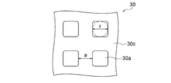
- the reinforcing sheet 30 has an opening 30a.
- the opening 30a allows the soluble adhesive layer 28 to contact or penetrate into the soluble adhesive layer 28 in a later step, and as a result, the reinforcing sheet 30 is peeled off by dissolution peeling or a method equivalent thereto. To make it easier. That is, it is possible to perform the peeling of the reinforcing sheet 30 that has played a role in an extremely short time while minimizing the stress applied to the multilayer laminate 26.
- the shape and size of the opening 30a are not particularly limited as long as they exhibit liquid permeability.
- the opening 30a is preferably a through hole. Typical examples of the shape of the through hole include various geometric shapes such as a circle (see, for example, FIG.
- the opening 30a may be a three-dimensional porous structure exhibiting liquid permeability, for example, a porous structure including a large number of open pores, or a three-dimensional network structure.
- the reinforcing sheet 30 preferably has a reinforcing region 30b and a liquid-permeable region 30c.
- the reinforcing region 30 b is a region where the opening 30 a does not exist, and is provided along at least the outer periphery of the reinforcing sheet 30. By not having the opening 30a, the reinforcing sheet 30 having the opening 30a can be prevented from becoming brittle, and the function as the reinforcing sheet 30 can be more effectively ensured.
- the liquid-permeable region 30c is a region including the opening 30a and is surrounded by the reinforcing region 30b.
- the liquid-permeable region 30c includes the opening 30a, thereby allowing contact or permeation of the solution, thereby facilitating peeling of the reinforcing sheet 30.
- the liquid-permeable region 30c may have a plurality of openings 30a. In this case, the region that connects the outer edges of the outermost openings 30a (typically located at the four corners) is liquid-permeable. Region 30c will be defined. Therefore, the liquid-permeable region 30c is typically rectangular.
- the reinforcing sheet 30 preferably has a porosity of 3 to 90%, more preferably 20 to 70%, and still more preferably 30 to 60%.
- the porosity is the ratio of the total pore volume in the liquid-permeable region 30c to the external volume of the reinforcing sheet 30, that is, ((total pore volume in the liquid-permeable region 30c) / (external shape of the reinforcing sheet 30). Volume)) ⁇ 100.
- the outer volume of the reinforcing sheet 30 is calculated with respect to the shape of the reinforcing sheet 30 when it is assumed that the reinforcing sheet 30 has no holes (that is, the opening 30a is completely closed). Virtual volume.
- the reinforcing sheet 30 (preferably the liquid-permeable region 30c) has a plurality of openings 30a having a predetermined shape arranged in accordance with a regular pattern as shown in FIGS.
- the solution can be uniformly contacted or penetrated into the reinforcing sheet 30 (particularly the liquid-permeable region 30c) without unevenness, and the reinforcing sheet 30 can be more easily peeled off.
- the distance a between the openings 30a closest to each other (hereinafter referred to as the primary proximity distance a) 0.025 to 50 mm is preferable, as shown in FIGS.
- the thickness is 1 to 10 mm, more preferably 0.2 to 4.0 mm.
- the ratio (a / T) of the primary proximity distance a (mm) to the thickness T (mm) of the reinforcing sheet 30 is preferably 0.025 to 1000, more preferably 0.1 to 500, and still more preferably. Is 0.2 to 300.
- the diameter r of the inscribed circle of the opening 30a as shown in FIGS. 5 and 6 is preferably 0.05 to 500 mm, more preferably 0.5 to 50 mm, still more preferably 1. 0 to 10 mm.
- the ratio (r / T) of the diameter r to the thickness T (mm) of the reinforcing sheet 30 is preferably 0.05 to 500, more preferably 0.1 to 300, and still more preferably 1.0. ⁇ 100. By making it within the preferred range, it is possible to promote the contact or penetration of the solution into the reinforcing sheet 30.
- the reinforcing sheet 30 has a Vickers hardness lower than that of the substrate 12.
- the reinforcing sheet 30 itself can bend, so that the stress that can be generated at the time of laminating or peeling can be released well.
- the multilayer laminate including the substrate 12 26 can be effectively prevented or suppressed.
- the Vickers hardness of the reinforcing sheet 30 is preferably 2 to 99% of the Vickers hardness of the substrate 12, more preferably 6 to 90%, and further preferably 10 to 85%.
- the reinforcing sheet 30 has a Vickers hardness of 50 to 700 HV
- the substrate 12 has a Vickers hardness of 500 to 3000 HV
- the reinforcing sheet 30 has a Vickers hardness of 150 to 550 HV
- the substrate 12 has a Vickers hardness of 550 to 2500 HV
- the reinforcing sheet 30 has a Vickers hardness of 200 to 500 HV
- the substrate 12 has a Vickers hardness of 600 to 2000 HV.
- the Vickers hardness is measured in accordance with the “Vickers hardness test” described in JIS Z 2244-2009.
- Vickers hardness HV of various materials is exemplified below: sapphire glass (2300 HV), cemented carbide (1700 HV), cermet (1650 HV), quartz (crystal) (1103 HV), SKH56 (high speed tool) Steel, high speed steel (722HV), tempered glass (640HV), SUS440C (stainless steel) (615HV), SUS630 (stainless steel) (375HV), titanium alloy 60 (64 alloy) (around 280HV), Inconel (heat resistant nickel) Alloy) (150 to 280HV), S45C (carbon steel for machine structure) (201 to 269HV), Hastelloy alloy (corrosion resistant nickel alloy) (100 to 230HV), SUS304 (stainless steel) (187HV), SUS430 (stainless steel) ( 183HV), cast iron 160 ⁇ 180 Hv), titanium alloy (110 ⁇ 150HV), brass (80 ⁇ 150HV), and bronze (50 ⁇ 100H
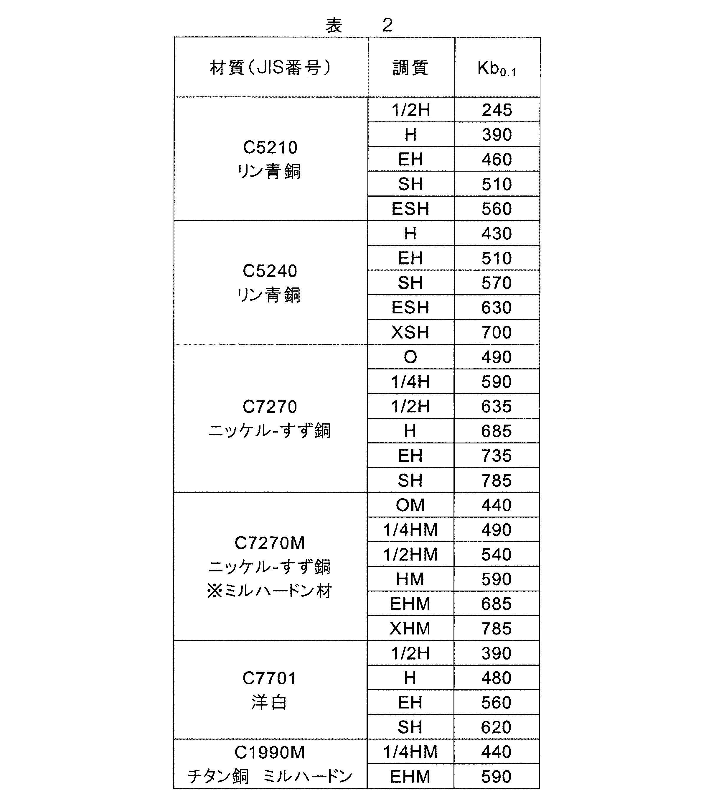
- the reinforcing sheet 30 preferably has a spring limit value Kb 0.1 of 100 to 1500 N / mm 2 , more preferably 150 to 1200 N / mm, measured in accordance with a repeated deflection test of JIS H 3130-2012. mm 2 , more preferably 200 to 1000 N / mm 2 .
- Kb 0.1 100 to 1500 N / mm 2 , more preferably 150 to 1200 N / mm, measured in accordance with a repeated deflection test of JIS H 3130-2012. mm 2 , more preferably 200 to 1000 N / mm 2 .
- the reinforcing sheet 30 when the reinforcing sheet 30 is laminated or peeled, the reinforcing sheet 30 itself bends, so that the stress that can be generated at the time of lamination or peeling can be released well. The bending of the body 26 can be prevented or suppressed more effectively.
- the reinforcing sheet 30 bent at the time of lamination or peeling can instantly return to its original flat shape by utilizing its elasticity, the flatness of the multilayer laminate 26 can be more effectively maintained. it can. Moreover, by utilizing the bending and elasticity of the reinforcing sheet 30, the reinforcing sheet 30 to which the peeling force is applied can be urged in the peeling direction (that is, the direction away from the multilayer laminate 26). Smoother peeling becomes possible.
- the material of the reinforcing sheet 30 is not particularly limited, but resin, metal, glass, or a combination thereof is preferable.
- the resin include an epoxy resin, a polyimide resin, a polyethylene resin, and a phenol resin, and a prepreg composed of such a resin and a fiber reinforcing material may be used.
- the metal include stainless steel and copper alloys (for example, bronze, phosphor copper, copper nickel alloy, copper titanium alloy) from the viewpoint of the above Vickers hardness and spring limit value Kb 0.1 .
- Stainless steel is particularly preferable from the viewpoint.
- the form of the reinforcing sheet 30 is not limited to a sheet shape as long as the bending of the multilayer laminate 26 can be prevented or suppressed, and may be other forms of films, plates, and foils, and preferably in the form of a sheet or a plate. is there.
- the reinforcing sheet 30 may be a laminate of these sheets, films, plates, foils, and the like. Typical examples of the reinforcing sheet 30 include a metal sheet, a resin sheet (particularly a hard resin sheet), and a glass sheet.
- the thickness of the reinforcing sheet 30 is preferably 10 ⁇ m to 1 mm, more preferably 50 to 800 ⁇ m, and still more preferably 100 to 600 ⁇ m from the viewpoint of maintaining the strength of the reinforcing sheet 30 and ease of handling of the reinforcing sheet 30.
- the reinforcing sheet 30 is a metal sheet (for example, a stainless steel sheet)
- the ten-point average roughness Rz-jis (JIS B 0601-2001) of the surface of the metal sheet on the side where the soluble adhesive layer 28 is formed. (Measured) is preferably 0.05 to 500 ⁇ m, more preferably 0.5 to 400 ⁇ m, still more preferably 1 to 300 ⁇ m. With such a surface roughness, it is considered that due to the anchor effect due to surface irregularities, the adhesion to the soluble adhesive layer 28 is increased, and the peel strength in the soluble adhesive layer 28 is improved.
- the structure of the soluble adhesive layer 28 is particularly limited as long as the reinforcing sheet 30 can be attached to the multilayer laminate 26 with desired adhesion and can be dissolved or softened by contact with a solution to be used later.
- the soluble adhesive layer 28 can be, for example, a known layer called an adhesive layer, an adhesive release layer, a release layer, or the like.
- the soluble pressure-sensitive adhesive layer 28 typically has adhesiveness, and therefore, it can be said that a pressure-sensitive adhesive layer or a pressure-sensitive adhesive release layer is typical. But the soluble adhesion layer 28 may be a peeling layer which does not have adhesiveness.
- the formation area of the soluble adhesion layer 28 can be appropriately adjusted within a range not impairing the effects of the present invention.
- FIG. 1 (d) it may be formed so as to cover the entire area of the surface of the multilayer laminate 26, or one of the opposed areas of the multilayer laminate 26 and the reinforcing sheet 30. It may be formed only in the region of the part (not shown).
- the soluble adhesive layer 28 preferably contains a solution-soluble resin, more preferably an acid-soluble resin or an alkali-soluble resin. Since this solution-soluble resin (for example, acid-soluble type or alkali-soluble type resin) can be efficiently dissolved or softened by contact with a solution (for example, acid solution or alkali solution), a later step The reinforcing sheet 30 can be peeled off more effectively. The peel strength of the reinforcing sheet 30 can be controlled by controlling the content of chemical soluble components and controlling the thickness of the resin layer.
- the acid-soluble resin include a resin composition in which silica, calcium carbonate, barium sulfate or the like, which is an acid-soluble filler, is filled at a high concentration of 60 wt% or more.
- Examples of the resin constituting this resin composition include epoxy resin, acrylic resin, methacrylic resin, melamine resin, polyester resin, styrene butadiene copolymer, acrylonitrile resin, polyimide resin and the like.
- Examples of the alkali-soluble resin include methacrylic acid polymers and acrylic acid polymers.
- Examples of the methacrylic acid polymer include methacrylic acid alkyl esters having an alkyl group having 1 to 18 carbon atoms.
- Examples of the acrylic acid polymer include alkyl acrylates having an alkyl group having 1 to 18 carbon atoms.
- the soluble adhesive layer 28 is preferably a layer that provides higher peel strength than the release layer 14.
- a method of comparing the magnitude relationship between the peel strengths of the soluble adhesive layer 28 and the release layer 14 there is a method of comparing the respective peel strength absolute values described later, but in a mode of peeling in the multilayer wiring board manufacturing process. Comparison by combined measurement is also effective.
- the peel strength of the release layer 14 is a yield strength when the substrate 12 is peeled off from the build-up wiring layer
- the peel strength of the soluble adhesive layer 28 is when the reinforcing sheet 30 is peeled from the multilayer laminate 26. It is also effective to compare the values measured as the yield strength.
- the peel strength of the soluble adhesive layer 28 is preferably 1.02 to 300 times the peel strength of the release layer 14, more preferably 1.05 to 100 times, still more preferably 3.0 to 50 times, and particularly preferably. Is 5.0 to 30 times.
- the peel strength of the soluble adhesive layer 28 is preferably 30 to 300 gf / cm, more preferably 40 to 250 gf / cm, still more preferably 50 to 175 gf / cm, and particularly preferably 70 to 150 gf / cm. .
- the peel strength of the soluble adhesive layer 28 can be measured basically in the same manner as the method for measuring the peel strength of the peel layer 14 described above, but refers to the peel strength measured before contact with the solution. It should be noted. Specifically, the peel strength of the soluble adhesive layer 28 is measured as follows. First, the soluble adhesive layer 28 is formed on the reinforcing sheet 30, and a copper foil having a thickness of 18 ⁇ m is laminated thereon to form a copper-clad laminate. Thereafter, in accordance with JIS C 6481-1996, the peel strength (gf / cm) when the copper foil is peeled is measured.
- the base material 12 is peeled from the metal layer 16 by the peeling layer 14 after the reinforcing sheet 30 is laminated and before the reinforcing sheet 30 is peeled off.
- the base material 12, the adhesion metal layer (if present), the peeling assist layer (if present), and the peeling layer 14 are peeled and removed. This peeling removal is preferably performed by physical peeling.
- the physical separation method is a method of separating the base material 12 and the like by peeling them from the build-up wiring layer by hand, jigs and tools, or the like.
- the reinforcing sheet 30 adhered through the soluble adhesive layer 28 reinforces the multilayer laminate 26, it is possible to prevent the multilayer laminate 26 from being greatly bent locally. That is, the reinforcing sheet 30 can reinforce the multilayer laminate 26 to resist the peeling force while the base material 12 is peeled, and can prevent or suppress the bending more effectively. Thus, disconnection and peeling of the wiring layer inside the build-up wiring layer that may be caused by bending can be avoided, and the connection reliability of the multilayer wiring layer can be improved. Moreover, the flatness (coplanarity) of the surface of the multilayer wiring layer can be improved by effectively preventing or suppressing the bending.
- the peelable strength of the soluble adhesive layer 28 is higher than that of the release layer 14, the release at the release layer 14 is more effectively avoided while the release at the soluble adhesive layer 28 is more effectively avoided when the substrate 12 is peeled off. It becomes easier to do. Therefore, the reinforcing sheet 30 that is in close contact with the multilayer laminate 26 via the soluble adhesive layer 28 can hold the adhesive state even more stably even when the substrate 12 is peeled off.
- Metal layer etching removal (optional process) If desired, the metal layer 16 is removed by etching before the reinforcing sheet 30 is peeled off, as shown in FIG. Etching of the metal layer 16 may be performed based on a known method such as flash etching.
- the process of mounting the chip after forming the build-up wiring layer in this way is a technique called RDL-First method.
- RDL-First method since the appearance inspection and the electrical inspection of the multilayer wiring layer 18 can be performed before the chip is mounted, the chip can be mounted only on the non-defective part while avoiding the defective part of each wiring layer.
- the RDL-First method is economically advantageous as compared to the Chip-First method, which is a method of sequentially laminating wiring layers on the surface of the chip, in that waste of the chip can be avoided.
- the product yield can be improved by performing the appearance inspection and electrical inspection on the wiring layer before chip mounting.
- a solder resist layer After the above-described steps, a solder resist layer, a surface metal treatment layer (for example, OSP (Organic Solderability Preservative) treatment layer, Au plating layer, Ni—Au plating layer) is formed on the surface of the first wiring layer 18 as necessary. Etc.), metal pillars for mounting electronic elements, and / or solder bumps may be formed.
- OSP Organic Solderability Preservative
- the multilayer laminate 26 is mounted on the surface opposite to the reinforcing sheet 30.
- the soluble pressure-sensitive adhesive layer 28 and the reinforcing sheet 30 excellent surface flatness (coplanarity) that is advantageous for mounting the electronic element 32 can be obtained. This can be realized on the surface of the build-up wiring layer including the wiring layer 18 as a buried electrode. That is, even when the electronic device 32 is mounted, the multilayer laminate 26 is not locally bent by the reinforcing sheet 30. As a result, the connection yield for mounting the electronic elements can be increased.
- Examples of the electronic element 32 include a semiconductor element, a chip capacitor, and a resistor.
- Examples of the electronic element mounting method include a flip chip mounting method and a die bonding method.
- the flip chip mounting method is a method in which the mounting pad of the electronic element 32 and the first wiring layer 18 are joined.
- a columnar electrode (pillar), a solder bump 34, or the like may be formed on the mounting pad as shown in FIG. 2G, and the sealing resin film 36 is formed on the surface including the first wiring layer 18 before mounting.
- NCF (Non-Conductive Film) or the like may be pasted.
- the joining is preferably performed using a low melting point metal such as solder, but an anisotropic conductive film or the like may be used.
- the die bonding adhesion method is a method in which the surface opposite to the mounting pad surface of the electronic element 32 is adhered to the first wiring layer 18.
- a paste or film which is a resin composition containing a thermosetting resin and a thermally conductive inorganic filler.
- the electronic element 32 is sealed with a sealing material 38 as shown in FIG. 2 (g) to further improve the rigidity of the entire laminate of the multilayer laminate 26 and the electronic element 32. It is preferable in that it can be performed.
- Dissolution or softening of soluble adhesive layer The solution is brought into contact with or penetrates into the soluble adhesive layer 28 through the opening 30a, thereby dissolving or softening the soluble adhesive layer 28.
- the dissolving liquid uses a liquid that can dissolve the soluble adhesive layer 28
- the soluble adhesive layer 28 is at least partially dissolved by contact with the dissolving liquid, thereby dissolving the soluble adhesive layer 28 in the soluble adhesive layer 28.
- the contact or penetration with the solution causes dissolution or softening of the soluble pressure-sensitive adhesive layer 28 and weakens or disables the adhesion between the multilayer laminate 26 and the reinforcing sheet 30.
- peeling of the reinforcing sheet 30 in the next step can be performed very easily using dissolution peeling or a technique based thereon. That is, the peeling of the reinforcing sheet 30 that has played a role can be performed in a very short time while minimizing the stress applied to the multilayer laminate 26.
- the solution is not particularly limited as long as it is a liquid that can dissolve the soluble adhesive layer 28, and various compositions or liquid chemicals can be used.
- the solution may be an acid solution.
- examples of such an acid solution include hydrochloric acid, nitric acid, sulfuric acid, and hydrofluoric acid.
- the solution may be an alkaline solution. Examples of such an alkaline solution include ethyl carboxylate (such as ethyl acetate), NaHCO 3 aqueous solution, Na 2 CO 3 aqueous solution, NaOH aqueous solution and the like.
- the reinforcing sheet 30 is peeled from the multilayer laminate 26 at the position of the soluble adhesive layer 28 to obtain the multilayer wiring board 40.
- the reinforcing sheet 30 is very easily peeled off due to the dissolution or softening of the soluble pressure-sensitive adhesive layer 28 (or, in some cases, it is partially peeled naturally), so it is reinforced with hands, jigs, tools, etc.
- the sheet 30 can be separated very easily by lightly peeling it from the multilayer laminate 26. Therefore, the reinforcing sheet 30 can be peeled off in a very short time while minimizing the stress applied to the multilayer laminate 26.
- the solution 30 can be used by utilizing the opening 30a. By facilitating contact with or permeating, it is possible to achieve a dramatic reduction in the time required for peeling the reinforcing sheet 30.
- the soluble adhesive layer 28 inherently has a higher peel strength than the release layer 14, the soluble adhesive layer 28 peels more than the release layer 14 unless special treatment is performed. It is difficult to do.
- the soluble adhesive layer 28 being dissolved or softened by contact or permeation with the dissolving solution, the adhesion between the multilayer laminate 26 and the reinforcing sheet 30 is weakened or neutralized. 30 can be easily peeled off.
- At least one side of the substrate 12 and / or the reinforcing sheet 30 extends from the end of the build-up wiring layer.
- the laminated sheet 10 that is optionally used in the method of the present invention includes a base material 12, a release layer 14, and a metal layer 16 in this order.
- the laminated sheet 10 may be in the form of a so-called copper foil with carrier.
- the material of the base 12 is not particularly limited, and may be any of glass, ceramics, resin, and metal. Moreover, the form of the base material 12 is not specifically limited, either, a sheet
- the substrate 12 may be a laminate of these sheets, films, plates, foils and the like. For example, the substrate 12 may function as a rigid support such as a glass plate, a ceramic plate, or a metal plate, or may have a non-rigid form such as a metal foil or a resin film. .
- the substrate 12 include a metal sheet, a glass sheet, a ceramic plate (plate), a laminate of a metal sheet and a prepreg, a metal sheet coated with an adhesive, and a resin sheet (particularly a hard resin sheet).
- Preferred examples of the metal of the substrate 12 include copper, titanium, nickel, stainless steel, aluminum and the like.
- Preferable examples of the ceramic include alumina, zirconia, silicon nitride, aluminum nitride (fine ceramics) and the like.
- the resin include epoxy resin, aramid resin, polyimide resin, nylon resin, liquid crystal polymer, PEEK resin, polyimide resin, polyamideimide resin, polyethersulfone resin, polyphenylene sulfide resin, PTFE resin, ETFE resin and the like. It is done. More preferably, the coefficient of thermal expansion (CTE) is less than 25 ppm / K (preferably 1.0 to 23 ppm / K, more preferably 1 from the viewpoint of preventing warpage of the coreless support due to heating when mounting the electronic device. 0.0 to 15 ppm / K, more preferably 1.0 to 10 ppm / K).
- the substrate 12 preferably has a Vickers hardness of 500 to 3000 HV, more preferably 550 to 2500 HV, and even more preferably 600 to 2000 HV.
- the substrate 12 is preferably made of a resin film, glass or ceramics, more preferably glass or ceramics, and particularly preferably glass.
- a glass sheet When glass is used as the substrate 12, it has advantages such as being light, having a low coefficient of thermal expansion, high insulation, being rigid and having a flat surface, so that the surface of the metal layer 16 can be made extremely smooth.
- the base material 12 when the base material 12 is glass, it has the surface flatness (coplanarity) advantageous at the time of electronic device mounting, and has chemical resistance in the desmear and various plating processes in the printed wiring board manufacturing process. There are advantages such as points.
- the glass constituting the substrate 12 include quartz glass, borosilicate glass, alkali-free glass, soda lime glass, aminosilicate glass, and combinations thereof, and alkali-free glass is particularly preferable.
- the alkali-free glass is a glass mainly containing silicon dioxide, aluminum oxide, boron oxide, and alkaline earth metal oxides such as calcium oxide and barium oxide, and further containing boric acid and substantially no alkali metal. That is.
- This alkali-free glass has a low and stable thermal expansion coefficient in the range of 3 to 5 ppm / K in a wide temperature range from 0 ° C to 350 ° C, so that the glass warpage is minimized when a semiconductor chip is mounted as an electronic element. There is an advantage that it can be limited.
- the thickness of the substrate 12 is preferably 100 to 2000 ⁇ m, more preferably 300 to 1800 ⁇ m, and still more preferably 400 to 1100 ⁇ m. When the thickness is within such a range, it is possible to reduce the thickness of the printed wiring board and reduce the warpage that occurs when mounting electronic components while ensuring an appropriate strength that does not hinder handling.
- the surface of the substrate 12 on the peeling layer 14 side (the adhesion metal layer side if present) has an arithmetic average roughness Ra of 0.1 to 70 nm, measured according to JIS B 0601-2001. It is preferably 0.5 to 60 nm, more preferably 1.0 to 50 nm, particularly preferably 1.5 to 40 nm, and most preferably 2.0 to 30 nm.
- the smaller the arithmetic average roughness the lower the average average roughness Ra on the surface of the metal layer 16 opposite to the release layer 14 (the outer surface of the metal layer 16).
- a highly miniaturized wiring pattern is formed such that the line / space (L / S) is 13 ⁇ m or less / 13 ⁇ m or less (for example, 12 ⁇ m / 12 ⁇ m to 1 ⁇ m / 1 ⁇ m). It is suitable to do.
- the laminated sheet 10 may have a close-contact metal layer and / or a release auxiliary layer on the surface of the base material 12 on the release layer 14 side, and preferably has the close-contact metal layer and the release auxiliary layer in this order.
- the adhesion metal layer provided as desired is preferably a layer composed of at least one metal selected from the group consisting of Ti, Cr and Ni, from the viewpoint of ensuring adhesion with the base material 12, It may be a pure metal or an alloy.
- the metal constituting the adhesion metal layer may contain inevitable impurities due to raw material components, film formation processes, and the like.
- the adhesion metal layer is preferably a layer formed by a vapor phase method such as sputtering.
- the adhesion metal layer is particularly preferably a layer formed by a magnetron sputtering method using a metal target because the uniformity of the film thickness distribution can be improved.
- the thickness of the adhesion metal layer is preferably 5 to 500 nm, more preferably 10 to 300 nm, still more preferably 18 to 200 nm, and particularly preferably 20 to 150 nm. This thickness is a value measured by analyzing the cross section of the layer with an energy dispersive X-ray spectrometer (TEM-EDX) of a transmission electron microscope.
- TEM-EDX energy dispersive X-ray spectrometer
- the peeling auxiliary layer provided as desired is a layer made of copper from the viewpoint of controlling the peeling strength with the peeling layer 14 to a desired value. Copper constituting the peeling assisting layer may contain inevitable impurities due to raw material components, film forming steps, and the like. In addition, when exposed to the atmosphere before and after the formation of the peeling assist layer, the presence of oxygen mixed therein is allowed. However, although not particularly limited, it is desirable that the adhesion metal layer and the peeling auxiliary layer are continuously formed without opening to the atmosphere.
- the peeling assist layer is preferably a layer formed by a vapor phase method such as sputtering.
- the peeling auxiliary layer is particularly preferably a layer formed by a magnetron sputtering method using a copper target from the viewpoint of improving the uniformity of the film thickness distribution.
- the thickness of the peeling assist layer is preferably 5 to 500 nm, more preferably 10 to 400 nm, still more preferably 15 to 300 nm, and particularly preferably 20 to 200 nm. This thickness is a value measured by analyzing the cross section of the layer with an energy dispersive X-ray spectrometer (TEM-EDX) of a transmission electron microscope.
- TEM-EDX energy dispersive X-ray spectrometer
- the material of the release layer 14 is not particularly limited as long as it is a layer that enables the substrate 12 to be peeled off.
- the peeling layer 14 can be comprised with the well-known material employ
- the release layer 14 may be either an organic release layer or an inorganic release layer. Examples of organic components used in the organic release layer include nitrogen-containing organic compounds, sulfur-containing organic compounds, carboxylic acids and the like. Examples of nitrogen-containing organic compounds include triazole compounds and imidazole compounds.
- examples of inorganic components used in the inorganic release layer include at least one metal oxide of Ni, Mo, Co, Cr, Fe, Ti, W, P, and Zn, a mixture of metal and nonmetal, carbon Layer and the like.
- the release layer 14 is preferably a layer mainly containing carbon from the viewpoint of ease of peeling and film formation, more preferably a layer mainly consisting of carbon or hydrocarbon, and more preferably It consists of amorphous carbon, which is a hard carbon film, or a carbon-nitrogen mixture.
- the release layer 14 (that is, the carbon layer) preferably has a carbon concentration measured by XPS of 60 atomic% or more, more preferably 70 atomic% or more, still more preferably 80 atomic% or more, and particularly preferably 85. It is at least atomic percent.
- the upper limit value of the carbon concentration is not particularly limited, and may be 100 atomic%, but 98 atomic% or less is realistic.
- the release layer 14 (particularly the carbon layer) can contain inevitable impurities (for example, oxygen, carbon, hydrogen, etc. derived from the surrounding environment such as the atmosphere). Further, metal atoms may be mixed into the release layer 14 (particularly the carbon layer) due to the film formation method of the metal layer 16.
- Carbon has low mutual diffusivity and reactivity with the base material 12 and is heated at a high temperature between the metal layer 16 (for example, a copper foil layer) and the bonding interface even when subjected to press working at a temperature exceeding 300 ° C. It is possible to prevent the metal bond from being formed and to maintain a state in which the substrate 12 is easily peeled and removed.
- This release layer 14 is also a layer formed by a vapor phase method such as sputtering, which suppresses excessive impurities in amorphous carbon, and continuous production with the formation of the adhesion metal layer and / or the release auxiliary layer described above. From the point of property etc., it is preferable.
- the thickness of the release layer 14 is preferably 1 to 20 nm, more preferably 1 to 10 nm. This thickness is a value measured by analyzing the cross section of the layer with an energy dispersive X-ray spectrometer (TEM-EDX) of a transmission electron microscope.
- TEM-EDX energy dispersive X-ray spectrometer
- the peeling strength of the peeling layer 14 is preferably 1 to 30 gf / cm. More preferably, it is 3 to 20 gf / cm, and further preferably 4 to 15 gf / cm.
- the peel strength of the release layer 14 is measured as follows. First, a release layer 14 is formed on a substrate 12, a laminated sheet is formed on which a copper layer as a metal layer 16 is formed, an electrolytic copper plating layer having a thickness of 18 ⁇ m is formed thereon, and copper-clad A laminated board is formed. Thereafter, in accordance with JIS C 6481-1996, the peel strength (gf / cm) when the electrolytic copper plating layer integrated with the metal layer 16 is peeled is measured.
- the peel strength of the release layer 14 can be controlled by controlling the thickness of the release layer 14, selecting the composition of the release layer 14, and the like.
- the metal layer 16 is a layer made of metal, and preferably includes a power feeding layer that enables power feeding to the first wiring layer 18 described later.
- the metal layer 16 or the power feeding layer may be manufactured by any method, for example, wet film formation methods such as electroless copper plating and electrolytic copper plating, physical vapor deposition methods such as sputtering and vacuum deposition, It may be a copper foil formed by chemical vapor deposition or a combination thereof.
- the preferred metal constituting the feed layer is copper, and therefore the preferred feed layer can be an ultra-thin copper layer.
- a particularly preferable power feeding layer is a copper layer formed by a vapor phase method such as sputtering or vacuum deposition from the viewpoint of easily supporting fine pitch by ultrathinning, and most preferably a copper layer manufactured by sputtering. It is.
- the ultra-thin copper layer is preferably a non-roughened copper layer, but pre-roughening, soft etching treatment, cleaning treatment, oxidation treatment, as long as it does not hinder the formation of wiring patterns during printed wiring board production.
- the secondary roughening may be caused by the reduction treatment.
- the thickness of the power feeding layer (for example, an ultrathin copper layer) constituting the metal layer 16 is not particularly limited, but is preferably 50 to 3000 nm, more preferably 70 to 2500 nm in order to cope with the fine pitch as described above. More preferably, it is 80 to 2000 nm, particularly preferably 90 to 1500 nm, particularly preferably 120 to 1000 nm, and most preferably 150 to 500 nm.
- a power feeding layer having a thickness within such a range (for example, an ultrathin copper layer) is manufactured by a sputtering method in terms of in-plane uniformity of film thickness and productivity in the form of a sheet or a roll. preferable.
- the surface of the metal layer 16 opposite to the release layer 14 has an arithmetic average roughness Ra of 1.0 to 100 nm, measured according to JIS B 0601-2001. It is preferably 2.0 to 40 nm, more preferably 3.0 to 35 nm, particularly preferably 4.0 to 30 nm, and most preferably 5.0 to 15 nm. In this way, the smaller the arithmetic average roughness, the line / space (L / S) is 13 ⁇ m or less / 13 ⁇ m or less (for example, 12 ⁇ m / 12 ⁇ m to 1 ⁇ m / 1 ⁇ m) in the printed wiring board manufactured using the laminated sheet 10. This is suitable for forming a highly miniaturized wiring pattern. In the case of such a smooth surface, it is preferable to employ a non-contact type surface roughness measurement method for measuring the arithmetic average roughness Ra.
- the metal layer 16 may have a layer configuration of two or more layers.
- the metal layer 16 may have an antireflection layer on the surface on the peeling layer 14 side of the power feeding layer in addition to the above power feeding layer. That is, the metal layer 16 may include a power feeding layer and an antireflection layer.
- the antireflection layer is preferably composed of at least one metal selected from the group consisting of Cr, W, Ta, Ti, Ni and Mo. It is preferable that at least the surface on the power feeding layer side of the antireflection layer is an aggregate of metal particles.
- the antireflection layer may have a layer structure composed entirely of an aggregate of metal particles, or a multilayer structure including a layer composed of an aggregate of metal particles and a non-particulate layer below the layer.
- the aggregate of metal particles constituting the surface on the power feeding layer side of the antireflection layer exhibits a desirable dark color due to its metallic material and granular form, and the dark color is between the wiring layer composed of copper. It provides the desired visual contrast and consequently improves visibility in image inspection (eg, automatic image inspection (AOI)). That is, the surface of the antireflection layer is visually recognized as black due to irregular reflection of light due to the convex shape of the metal particles.
- AOI automatic image inspection
- the antireflection layer has excellent adhesion and peeling properties to the release layer 14 and excellent adhesion to the power feeding layer, and also has excellent peeling resistance to the developer during the formation of the photoresist layer.
- the glossiness Gs (60 °) of the surface on the power feeding layer side of the antireflection layer is preferably 500 or less, more preferably 450 or less, still more preferably 400 or less, Particularly preferred is 350 or less, and most preferred is 300 or less.
- the lower limit of the glossiness Gs (60 °) is preferably as low as possible, and is not particularly limited. However, the glossiness Gs (60 °) on the surface of the antireflection layer on the power feeding layer side is actually 100 or more. More realistically, it is 150 or more.
- the specular gloss Gs (60 °) by image analysis of the roughened particles can be measured using a commercially available gloss meter in accordance with JIS Z 8741-1997 (mirror gloss-measurement method).
- the surface of the antireflection layer on the power feeding layer side is a metal whose projected area equivalent circle diameter determined by SEM image analysis is 10 to 100 nm. It is preferably composed of an aggregate of particles, more preferably 25 to 100 nm, still more preferably 65 to 95 nm.
- a projected area equivalent circle diameter can be measured by photographing the surface of the antireflection layer with a scanning electron microscope at a predetermined magnification (eg, 50000 times) and analyzing the obtained SEM image. Specifically, an arithmetic average value of the projected area equivalent circle diameter measured using commercially available image analysis type particle size distribution software (for example, Mactech-VIEW, manufactured by Mounttech Co., Ltd.) is adopted.
- the antireflection layer is composed of at least one metal selected from Cr, W, Ta, Ti, Ni and Mo, preferably at least one metal selected from Ta, Ti, Ni and Mo, and more Preferably it is at least one metal selected from Ti, Ni and Mo, most preferably composed of Ti. These metals may be pure metals or alloys. In any case, it is preferred that these metals are essentially unoxidized (essentially not metal oxides) because they exhibit a desirable dark color that improves visual contrast with Cu, specifically reflective
- the oxygen content of the prevention layer is preferably 0 to 15 atomic%, more preferably 0 to 13 atomic%, and still more preferably 1 to 10 atomic%.
- the metal has a property that it does not dissolve in the copper flash etching solution, and as a result, can exhibit excellent chemical resistance with respect to the copper flash etching solution.
- the thickness of the antireflection layer is preferably 1 to 500 nm, more preferably 10 to 300 nm, still more preferably 20 to 200 nm, and particularly preferably 30 to 150 nm.
Landscapes
- Engineering & Computer Science (AREA)
- Manufacturing & Machinery (AREA)
- Microelectronics & Electronic Packaging (AREA)
- Production Of Multi-Layered Print Wiring Board (AREA)
- Physics & Mathematics (AREA)
- Geometry (AREA)
Abstract
Description
前記多層積層体の一方の面に、可溶性粘着層を介して、開口部を有する補強シートを積層する工程と、
前記開口部を介して、前記可溶性粘着層を溶解可能な液体を、前記可溶性粘着層に接触又は浸透させ、それにより前記可溶性粘着層を溶解又は軟化させる工程と、
前記補強シートを前記多層積層体から前記可溶性粘着層の位置で剥離して多層配線板を得る工程と、
を含む、多層配線板の製造方法が提供される。
本発明による多層配線板の製造方法は、(1)所望により用いられる積層シートの用意、(2)多層積層体の作製、(3)補強シートの積層、(4)所望により行われる基材の剥離、(5)所望により行われる金属層のエッチング除去、(6)所望により行われる第1配線層の表面処理、(7)所望により行われる電子素子の搭載、(8)可溶性粘着層の溶解又は軟化、及び(9)補強シートの剥離の各工程を含む。
所望により、図1(a)に示されるように、多層配線板を形成するためのベースとなる積層シート10を用意する。積層シート10は、基材12、剥離層14及び金属層16を順に備える。積層シート10は、いわゆるキャリア付銅箔の形態であってもよい。積層シート10の本発明の好ましい態様については後述するものとする。
図1(b)及び(c)に示されるように、配線層18及び絶縁層20を交互に形成して多層積層体26を作製する。図1(b)及び(c)に示される配線層18及び絶縁層20で構成される逐次積層構造は、ビルドアップ層ないしビルドアップ配線層と一般的に称されるものであるが、本発明の製造方法においては、一般的にプリント配線板において採用される公知のビルドアップ配線層の構成のみからなる多層積層体の形成方法のみならず、予め形成されたバンプ付の多層積層体の一部となる積層体を、絶縁性接着剤を介して積層する方法等も採用することができ、特に限定されない。
図1(d)に示されるように、多層積層体26の一方の面(例えば多層積層体26の積層シート10と反対側の表面)に可溶性粘着層28を介して補強シート30を積層する。これにより、多層積層体26は補強シート30によって局部的に大きく湾曲されないように補強されることができる。すなわち、剥離時や湾曲が効果的に防止ないし抑制される。こうして、湾曲により引き起こされることがあるビルドアップ配線層内部の配線層の断線や剥離を回避して、多層配線層の接続信頼性を向上することができる。また、湾曲が効果的に防止ないし抑制されることで、多層配線層表面の平坦性(コプラナリティ)を向上することができる。

積層シート10を用いる場合、図2(e)に示されるように、補強シート30の積層後で、かつ、補強シート30の剥離前に、基材12を金属層16から剥離層14で剥離するのが好ましい。すなわち、基材12、密着金属層(存在する場合)、剥離補助層(存在する場合)、及び剥離層14が剥離除去される。この剥離除去は、物理的な剥離により行われるのが好ましい。物理的分離法は、手や治工具、機械等で基材12等をビルドアップ配線層から引き剥がすことにより分離する手法である。このとき、可溶性粘着層28を介して密着した補強シート30が多層積層体26を補強していることで、多層積層体26が局部的に大きく湾曲するのを防止することができる。すなわち、補強シート30は、基材12が剥離される間、引き剥がし力に抗すべく多層積層体26を補強し、湾曲をより一層効果的に防止ないし抑制することができる。こうして、湾曲により引き起こされることがあるビルドアップ配線層内部の配線層の断線や剥離を回避して、多層配線層の接続信頼性を向上することができる。また、湾曲が効果的に防止ないし抑制されることで、多層配線層表面の平坦性(コプラナリティ)を向上することができる。
所望により、図2(f)に示されるように、補強シート30の剥離前に、金属層16をエッチングにより除去する。金属層16のエッチングは、フラッシュエッチング等の公知の手法に基づき行えばよい。
上記工程の後、必要に応じて、第1配線層18の表面には、ソルダ―レジスト層、表面金属処理層(例えば、OSP(Organic Solderbility Preservative)処理層、Auめっき層、Ni-Auめっき層等)、電子素子搭載用の金属ピラー、及び/又ははんだバンプ等が形成されていてもよい。
所望により、図2(g)に示されるように、補強シート30の積層後(或いは金属層16の除去又はその後の電気検査後)で、かつ、補強シート30の剥離前に、多層積層体26の補強シート30と反対側の表面に電子素子32を搭載させる。本発明の製造方法においては、可溶性粘着層28及び補強シート30を採用することで、電子素子32の搭載に有利となる優れた表面平坦性(コプラナリティ)を多層積層体26の表面(例えば第1配線層18を埋込み電極として含むビルドアップ配線層の表面)において実現することができる。すなわち、電子素子32の搭載時においても、多層積層体26は補強シート30によって局部的に大きく湾曲されずに済む。その結果、電子素子搭載の接続歩留まりを高くすることができる。
開口部30aを介して溶解液を可溶性粘着層28に接触又は浸透させ、それにより可溶性粘着層28を溶解又は軟化させる。前述のとおり、溶解液は可溶性粘着層28を溶解可能な液体を用いているため、可溶性粘着層28は溶解液と接触することで少なくとも部分的に溶解し、それによって可溶性粘着層28に溶解液が浸透しうる。そして、かかる溶解液との接触又は浸透は、可溶性粘着層28の溶解又は軟化をもたらし、多層積層体26と補強シート30との密着力を弱める又は無力化する。こうして、次の工程における補強シート30の剥離を、溶解剥離又はそれに準じた手法を用いて、極めて容易に行うことができる。すなわち、役目を果たした補強シート30の剥離を多層積層体26に与える応力を最小化しながら極めて短時間で行うことができる。
図3(h)及び(i)に示されるように、補強シート30を多層積層体26から可溶性粘着層28の位置で剥離して多層配線板40を得る。補強シート30は可溶性粘着層28の溶解又は軟化に起因して極めて剥離しやすい状態となっている(又は場合によっては部分的に自然剥離している)ため、手や治工具、機械等で補強シート30を多層積層体26から軽く引き剥がすことにより極めて容易に分離することができる。したがって、多層積層体26に与える応力を最小化しながら極めて短時間で補強シート30の剥離を行うことができる。こうして多層積層体26に加わる応力が最小化されることで、多層配線板40における配線の断線や実装部の断線を効果的に回避することができる。また、上記応力の低減のために可溶性粘着層28を用いることを考えたとしても、それだけでは溶剤剥離に多大な時間を要するところ、本発明の方法によれば開口部30aを活用して溶解液との接触又は浸透を促進することで、補強シート30の剥離に要する時間の飛躍的な短縮化を実現することができる。
基材12及び/又は補強シート30の少なくとも一辺がビルドアップ配線層の端部から延出しているのが好ましい。こうすることで、基材ないし補強シートを剥離する際、端部を把持することが可能となり、剥離を容易にすることができるとの利点がある。
前述したとおり、本発明の方法において所望により用いられる積層シート10は、基材12、剥離層14及び金属層16を順に備える。積層シート10は、いわゆるキャリア付銅箔の形態であってもよい。
Claims (9)
- 配線層及び絶縁層を交互に形成して多層積層体を作製する工程と、
前記多層積層体の一方の面に、可溶性粘着層を介して、開口部を有する補強シートを積層する工程と、
前記開口部を介して、前記可溶性粘着層を溶解可能な液体を、前記可溶性粘着層に接触又は浸透させ、それにより前記可溶性粘着層を溶解又は軟化させる工程と、
前記補強シートを前記多層積層体から前記可溶性粘着層の位置で剥離して多層配線板を得る工程と、
を含む、多層配線板の製造方法。 - 前記補強シートが、
前記補強シートの少なくとも外周に沿って設けられ、前記開口部が存在しない補強領域と、
前記補強領域によって囲まれ、前記開口部を含む通液性領域と、
を有する、請求項1に記載の方法。 - 前記補強シートは3~90%の空孔率を有し、前記空孔率は、前記補強シートの外形体積に対する、前記通液性領域における総空孔体積の割合である、請求項2に記載の方法。
- 前記可溶性粘着層が溶液可溶型樹脂を含む、請求項1~3のいずれか一項に記載の方法。
- 前記可溶性粘着層が酸可溶型樹脂又はアルカリ可溶型樹脂を含む、請求項1~4のいずれか一項に記載の方法。
- 前記補強シートの積層後で、かつ、前記補強シートの剥離前に、前記多層積層体の補強シートと反対側の表面に電子素子を搭載させる工程をさらに含む、請求項1~5のいずれか一項に記載の方法。
- 前記多層積層体が、基材、剥離層及び金属層をこの順に備えた積層シートの前記金属層の表面に作製される、請求項1~6のいずれか一項に記載の方法。
- 前記補強シートの積層後で、かつ、前記補強シートの剥離前に、前記基材を前記金属層から前記剥離層で剥離する工程をさらに含む、請求項7に記載の方法。
- 前記補強シートの剥離前に、前記金属層をエッチングにより除去する工程をさらに含む、請求項7又は8に記載の方法。
Priority Applications (5)
| Application Number | Priority Date | Filing Date | Title |
|---|---|---|---|
| CN202310741588.5A CN116709672A (zh) | 2016-11-28 | 2017-11-24 | 多层布线板的制造方法 |
| KR1020197012599A KR20190088465A (ko) | 2016-11-28 | 2017-11-24 | 다층 배선판의 제조 방법 |
| US16/463,552 US11527415B2 (en) | 2016-11-28 | 2017-11-24 | Multilayer circuit board manufacturing method |
| CN201780073261.8A CN109997419A (zh) | 2016-11-28 | 2017-11-24 | 多层布线板的制造方法 |
| JP2018552984A JP7112962B2 (ja) | 2016-11-28 | 2017-11-24 | 多層配線板の製造方法 |
Applications Claiming Priority (2)
| Application Number | Priority Date | Filing Date | Title |
|---|---|---|---|
| JP2016-230539 | 2016-11-28 | ||
| JP2016230539 | 2016-11-28 |
Publications (1)
| Publication Number | Publication Date |
|---|---|
| WO2018097264A1 true WO2018097264A1 (ja) | 2018-05-31 |
Family
ID=62195095
Family Applications (1)
| Application Number | Title | Priority Date | Filing Date |
|---|---|---|---|
| PCT/JP2017/042288 Ceased WO2018097264A1 (ja) | 2016-11-28 | 2017-11-24 | 多層配線板の製造方法 |
Country Status (6)
| Country | Link |
|---|---|
| US (1) | US11527415B2 (ja) |
| JP (1) | JP7112962B2 (ja) |
| KR (1) | KR20190088465A (ja) |
| CN (2) | CN116709672A (ja) |
| TW (1) | TW201828788A (ja) |
| WO (1) | WO2018097264A1 (ja) |
Cited By (7)
| Publication number | Priority date | Publication date | Assignee | Title |
|---|---|---|---|---|
| WO2020105482A1 (ja) * | 2018-11-21 | 2020-05-28 | 三井金属鉱業株式会社 | 半導体パッケージの製造方法及びそれに用いられる粘着シート |
| WO2020105485A1 (ja) * | 2018-11-21 | 2020-05-28 | 三井金属鉱業株式会社 | 半導体パッケージの製造方法 |
| JP2021044447A (ja) * | 2019-09-12 | 2021-03-18 | 株式会社東芝 | キャリア及び半導体装置の製造方法 |
| TWI737215B (zh) * | 2019-04-29 | 2021-08-21 | 大陸商深超光電(深圳)有限公司 | 重佈線路結構的製備方法 |
| WO2024154787A1 (ja) * | 2023-01-18 | 2024-07-25 | 大日本印刷株式会社 | 配線基板群及びその製造方法並びに配線基板及びその製造方法 |
| WO2024214797A1 (ja) * | 2023-04-11 | 2024-10-17 | 大日本印刷株式会社 | 第1配線基板群、第2配線基板群、配線基板及び配線基板の製造方法 |
| CN119833417A (zh) * | 2024-12-09 | 2025-04-15 | 北京芯力技术创新中心有限公司 | 芯片封装结构及其制备方法、电子设备 |
Families Citing this family (6)
| Publication number | Priority date | Publication date | Assignee | Title |
|---|---|---|---|---|
| KR102163059B1 (ko) * | 2018-09-07 | 2020-10-08 | 삼성전기주식회사 | 연결구조체 내장기판 |
| JP7253946B2 (ja) * | 2019-03-20 | 2023-04-07 | 新光電気工業株式会社 | 配線基板及びその製造方法、半導体パッケージ |
| WO2022102182A1 (ja) * | 2020-11-11 | 2022-05-19 | 三井金属鉱業株式会社 | 配線基板の製造方法 |
| US11923285B2 (en) | 2021-01-05 | 2024-03-05 | Advanced Semiconductor Engineering, Inc. | Electronic device package and method of manufacturing the same |
| CN116230563B (zh) * | 2023-02-28 | 2026-03-13 | 深圳市矩阵多元科技有限公司 | 封装结构制造方法及封装结构 |
| JP7662910B1 (ja) | 2023-07-13 | 2025-04-15 | 三井金属鉱業株式会社 | 接着性積層シート、積層体、及び配線板の製造方法 |
Citations (5)
| Publication number | Priority date | Publication date | Assignee | Title |
|---|---|---|---|---|
| JP2003158239A (ja) * | 2001-11-22 | 2003-05-30 | Sony Corp | マルチチップ回路モジュール及びその製造方法 |
| JP2005191550A (ja) * | 2003-12-01 | 2005-07-14 | Tokyo Ohka Kogyo Co Ltd | 基板の貼り付け方法 |
| JP2007150002A (ja) * | 2005-11-29 | 2007-06-14 | Tdk Corp | 半導体ic内蔵基板及びその製造方法 |
| JP2011508448A (ja) * | 2007-12-27 | 2011-03-10 | フリースケール セミコンダクター インコーポレイテッド | 電子アセンブリ製造方法 |
| JP2016167487A (ja) * | 2015-03-09 | 2016-09-15 | 富士通株式会社 | 配線基板の製造方法 |
Family Cites Families (12)
| Publication number | Priority date | Publication date | Assignee | Title |
|---|---|---|---|---|
| JP4273895B2 (ja) | 2003-09-24 | 2009-06-03 | 日立化成工業株式会社 | 半導体素子搭載用パッケージ基板の製造方法 |
| US8188375B2 (en) * | 2005-11-29 | 2012-05-29 | Tok Corporation | Multilayer circuit board and method for manufacturing the same |
| JP5324051B2 (ja) | 2007-03-29 | 2013-10-23 | 新光電気工業株式会社 | 配線基板の製造方法及び半導体装置の製造方法及び配線基板 |
| US8828525B2 (en) * | 2010-09-13 | 2014-09-09 | Kaneka Corporation | Flexible printed circuit board integrated with reinforcing plate, and method for manufacturing flexible printed circuit board integrated with reinforcing plate |
| JP5864180B2 (ja) | 2011-09-21 | 2016-02-17 | 新光電気工業株式会社 | 半導体パッケージ及びその製造方法 |
| JP5225451B2 (ja) * | 2011-11-04 | 2013-07-03 | 新光電気工業株式会社 | 配線基板の製造方法及び半導体パッケージの製造方法 |
| JP5913914B2 (ja) * | 2011-11-08 | 2016-04-27 | 東京応化工業株式会社 | 基板処理装置及び基板処理方法 |
| JP2015035551A (ja) | 2013-08-09 | 2015-02-19 | ルネサスエレクトロニクス株式会社 | 半導体装置の製造方法 |
| JP6201610B2 (ja) | 2013-10-08 | 2017-09-27 | 富士通株式会社 | 電子装置の製造方法及び回路基板 |
| TWI488549B (zh) * | 2014-03-07 | 2015-06-11 | Azotek Co Ltd | 金屬基板及其製作方法 |
| JP6299290B2 (ja) | 2014-03-07 | 2018-03-28 | 富士通株式会社 | 回路基板の製造方法 |
| JP6456292B2 (ja) * | 2014-10-30 | 2019-01-23 | 三井金属鉱業株式会社 | キャリア付銅箔及びそれを用いたプリント配線板の製造方法 |
-
2017
- 2017-11-24 JP JP2018552984A patent/JP7112962B2/ja active Active
- 2017-11-24 US US16/463,552 patent/US11527415B2/en active Active
- 2017-11-24 CN CN202310741588.5A patent/CN116709672A/zh active Pending
- 2017-11-24 CN CN201780073261.8A patent/CN109997419A/zh active Pending
- 2017-11-24 KR KR1020197012599A patent/KR20190088465A/ko not_active Withdrawn
- 2017-11-24 WO PCT/JP2017/042288 patent/WO2018097264A1/ja not_active Ceased
- 2017-11-24 TW TW106140871A patent/TW201828788A/zh unknown
Patent Citations (5)
| Publication number | Priority date | Publication date | Assignee | Title |
|---|---|---|---|---|
| JP2003158239A (ja) * | 2001-11-22 | 2003-05-30 | Sony Corp | マルチチップ回路モジュール及びその製造方法 |
| JP2005191550A (ja) * | 2003-12-01 | 2005-07-14 | Tokyo Ohka Kogyo Co Ltd | 基板の貼り付け方法 |
| JP2007150002A (ja) * | 2005-11-29 | 2007-06-14 | Tdk Corp | 半導体ic内蔵基板及びその製造方法 |
| JP2011508448A (ja) * | 2007-12-27 | 2011-03-10 | フリースケール セミコンダクター インコーポレイテッド | 電子アセンブリ製造方法 |
| JP2016167487A (ja) * | 2015-03-09 | 2016-09-15 | 富士通株式会社 | 配線基板の製造方法 |
Cited By (18)
| Publication number | Priority date | Publication date | Assignee | Title |
|---|---|---|---|---|
| JP7289852B2 (ja) | 2018-11-21 | 2023-06-12 | 三井金属鉱業株式会社 | 半導体パッケージの製造方法及びそれに用いられる粘着シート |
| KR102667581B1 (ko) | 2018-11-21 | 2024-05-22 | 미쓰이금속광업주식회사 | 반도체 패키지의 제조 방법 |
| KR102667583B1 (ko) | 2018-11-21 | 2024-05-22 | 미쓰이금속광업주식회사 | 반도체 패키지의 제조 방법 및 그것에 사용되는 점착 시트 |
| KR20210093852A (ko) * | 2018-11-21 | 2021-07-28 | 미쓰이금속광업주식회사 | 반도체 패키지의 제조 방법 및 그것에 사용되는 점착 시트 |
| KR20210093853A (ko) * | 2018-11-21 | 2021-07-28 | 미쓰이금속광업주식회사 | 반도체 패키지의 제조 방법 |
| WO2020105482A1 (ja) * | 2018-11-21 | 2020-05-28 | 三井金属鉱業株式会社 | 半導体パッケージの製造方法及びそれに用いられる粘着シート |
| JPWO2020105485A1 (ja) * | 2018-11-21 | 2021-09-30 | 三井金属鉱業株式会社 | 半導体パッケージの製造方法 |
| JPWO2020105482A1 (ja) * | 2018-11-21 | 2021-10-14 | 三井金属鉱業株式会社 | 半導体パッケージの製造方法及びそれに用いられる粘着シート |
| WO2020105485A1 (ja) * | 2018-11-21 | 2020-05-28 | 三井金属鉱業株式会社 | 半導体パッケージの製造方法 |
| JP7382342B2 (ja) | 2018-11-21 | 2023-11-16 | 三井金属鉱業株式会社 | 半導体パッケージの製造方法 |
| US11935865B2 (en) | 2018-11-21 | 2024-03-19 | Mitsui Mining & Smelting Co., Ltd. | Semiconductor package manufacturing method, and adhesive sheet used therein |
| US11876070B2 (en) | 2018-11-21 | 2024-01-16 | Mitsui Mining & Smelting Co., Ltd. | Semiconductor package manufacturing method |
| TWI737215B (zh) * | 2019-04-29 | 2021-08-21 | 大陸商深超光電(深圳)有限公司 | 重佈線路結構的製備方法 |
| JP7362378B2 (ja) | 2019-09-12 | 2023-10-17 | 株式会社東芝 | キャリア及び半導体装置の製造方法 |
| JP2021044447A (ja) * | 2019-09-12 | 2021-03-18 | 株式会社東芝 | キャリア及び半導体装置の製造方法 |
| WO2024154787A1 (ja) * | 2023-01-18 | 2024-07-25 | 大日本印刷株式会社 | 配線基板群及びその製造方法並びに配線基板及びその製造方法 |
| WO2024214797A1 (ja) * | 2023-04-11 | 2024-10-17 | 大日本印刷株式会社 | 第1配線基板群、第2配線基板群、配線基板及び配線基板の製造方法 |
| CN119833417A (zh) * | 2024-12-09 | 2025-04-15 | 北京芯力技术创新中心有限公司 | 芯片封装结构及其制备方法、电子设备 |
Also Published As
| Publication number | Publication date |
|---|---|
| US20190378727A1 (en) | 2019-12-12 |
| TW201828788A (zh) | 2018-08-01 |
| CN116709672A (zh) | 2023-09-05 |
| JPWO2018097264A1 (ja) | 2019-10-17 |
| KR20190088465A (ko) | 2019-07-26 |
| CN109997419A (zh) | 2019-07-09 |
| US11527415B2 (en) | 2022-12-13 |
| JP7112962B2 (ja) | 2022-08-04 |
Similar Documents
| Publication | Publication Date | Title |
|---|---|---|
| JP7208011B2 (ja) | 多層配線板の製造方法 | |
| JP7112962B2 (ja) | 多層配線板の製造方法 | |
| JP6415760B2 (ja) | キャリア付銅箔、並びに配線層付コアレス支持体及びプリント配線板の製造方法 | |
| KR102179806B1 (ko) | 다층 배선판의 제조 방법 | |
| KR102179799B1 (ko) | 다층 배선판의 제조 방법 | |
| JP7212210B2 (ja) | 配線基板の製造方法 | |
| JP6793755B2 (ja) | 多層配線板の製造方法 | |
| KR102225796B1 (ko) | 배선판의 제조 방법 |
Legal Events
| Date | Code | Title | Description |
|---|---|---|---|
| 121 | Ep: the epo has been informed by wipo that ep was designated in this application |
Ref document number: 17873072 Country of ref document: EP Kind code of ref document: A1 |
|
| ENP | Entry into the national phase |
Ref document number: 2018552984 Country of ref document: JP Kind code of ref document: A |
|
| ENP | Entry into the national phase |
Ref document number: 20197012599 Country of ref document: KR Kind code of ref document: A |
|
| NENP | Non-entry into the national phase |
Ref country code: DE |
|
| 122 | Ep: pct application non-entry in european phase |
Ref document number: 17873072 Country of ref document: EP Kind code of ref document: A1 |