WO2017169458A1 - 清浄度評価方法、洗浄条件決定方法、およびシリコンウェーハの製造方法 - Google Patents
清浄度評価方法、洗浄条件決定方法、およびシリコンウェーハの製造方法 Download PDFInfo
- Publication number
- WO2017169458A1 WO2017169458A1 PCT/JP2017/007749 JP2017007749W WO2017169458A1 WO 2017169458 A1 WO2017169458 A1 WO 2017169458A1 JP 2017007749 W JP2017007749 W JP 2017007749W WO 2017169458 A1 WO2017169458 A1 WO 2017169458A1
- Authority
- WO
- WIPO (PCT)
- Prior art keywords
- silicon carbide
- silicon wafer
- cleanliness
- manufacturing
- carbide surface
- Prior art date
- Legal status (The legal status is an assumption and is not a legal conclusion. Google has not performed a legal analysis and makes no representation as to the accuracy of the status listed.)
- Ceased
Links
Classifications
-
- G—PHYSICS
- G01—MEASURING; TESTING
- G01N—INVESTIGATING OR ANALYSING MATERIALS BY DETERMINING THEIR CHEMICAL OR PHYSICAL PROPERTIES
- G01N1/00—Sampling; Preparing specimens for investigation
- G01N1/28—Preparing specimens for investigation including physical details of (bio-)chemical methods covered elsewhere, e.g. G01N33/50, C12Q
- G01N1/32—Polishing; Etching
-
- G—PHYSICS
- G01—MEASURING; TESTING
- G01N—INVESTIGATING OR ANALYSING MATERIALS BY DETERMINING THEIR CHEMICAL OR PHYSICAL PROPERTIES
- G01N27/00—Investigating or analysing materials by the use of electric, electrochemical, or magnetic means
- G01N27/62—Investigating or analysing materials by the use of electric, electrochemical, or magnetic means by investigating the ionisation of gases, e.g. aerosols; by investigating electric discharges, e.g. emission of cathode
- G01N27/622—Ion mobility spectrometry
- G01N27/623—Ion mobility spectrometry combined with mass spectrometry
-
- C—CHEMISTRY; METALLURGY
- C04—CEMENTS; CONCRETE; ARTIFICIAL STONE; CERAMICS; REFRACTORIES
- C04B—LIME, MAGNESIA; SLAG; CEMENTS; COMPOSITIONS THEREOF, e.g. MORTARS, CONCRETE OR LIKE BUILDING MATERIALS; ARTIFICIAL STONE; CERAMICS; REFRACTORIES; TREATMENT OF NATURAL STONE
- C04B35/00—Shaped ceramic products characterised by their composition; Ceramics compositions; Processing powders of inorganic compounds preparatory to the manufacturing of ceramic products
- C04B35/515—Shaped ceramic products characterised by their composition; Ceramics compositions; Processing powders of inorganic compounds preparatory to the manufacturing of ceramic products based on non-oxide ceramics
- C04B35/56—Shaped ceramic products characterised by their composition; Ceramics compositions; Processing powders of inorganic compounds preparatory to the manufacturing of ceramic products based on non-oxide ceramics based on carbides or oxycarbides
- C04B35/565—Shaped ceramic products characterised by their composition; Ceramics compositions; Processing powders of inorganic compounds preparatory to the manufacturing of ceramic products based on non-oxide ceramics based on carbides or oxycarbides based on silicon carbide
-
- C—CHEMISTRY; METALLURGY
- C23—COATING METALLIC MATERIAL; COATING MATERIAL WITH METALLIC MATERIAL; CHEMICAL SURFACE TREATMENT; DIFFUSION TREATMENT OF METALLIC MATERIAL; COATING BY VACUUM EVAPORATION, BY SPUTTERING, BY ION IMPLANTATION OR BY CHEMICAL VAPOUR DEPOSITION, IN GENERAL; INHIBITING CORROSION OF METALLIC MATERIAL OR INCRUSTATION IN GENERAL
- C23C—COATING METALLIC MATERIAL; COATING MATERIAL WITH METALLIC MATERIAL; SURFACE TREATMENT OF METALLIC MATERIAL BY DIFFUSION INTO THE SURFACE, BY CHEMICAL CONVERSION OR SUBSTITUTION; COATING BY VACUUM EVAPORATION, BY SPUTTERING, BY ION IMPLANTATION OR BY CHEMICAL VAPOUR DEPOSITION, IN GENERAL
- C23C16/00—Chemical coating by decomposition of gaseous compounds, without leaving reaction products of surface material in the coating, i.e. chemical vapour deposition [CVD] processes
- C23C16/44—Chemical coating by decomposition of gaseous compounds, without leaving reaction products of surface material in the coating, i.e. chemical vapour deposition [CVD] processes characterised by the method of coating
- C23C16/4401—Means for minimising impurities, e.g. dust, moisture or residual gas, in the reaction chamber
- C23C16/4407—Cleaning of reactor or reactor parts by using wet or mechanical methods
-
- C—CHEMISTRY; METALLURGY
- C30—CRYSTAL GROWTH
- C30B—SINGLE-CRYSTAL GROWTH; UNIDIRECTIONAL SOLIDIFICATION OF EUTECTIC MATERIAL OR UNIDIRECTIONAL DEMIXING OF EUTECTOID MATERIAL; REFINING BY ZONE-MELTING OF MATERIAL; PRODUCTION OF A HOMOGENEOUS POLYCRYSTALLINE MATERIAL WITH DEFINED STRUCTURE; SINGLE CRYSTALS OR HOMOGENEOUS POLYCRYSTALLINE MATERIAL WITH DEFINED STRUCTURE; AFTER-TREATMENT OF SINGLE CRYSTALS OR A HOMOGENEOUS POLYCRYSTALLINE MATERIAL WITH DEFINED STRUCTURE; APPARATUS THEREFOR
- C30B23/00—Single-crystal growth by condensing evaporated or sublimed materials
- C30B23/02—Epitaxial-layer growth
-
- C—CHEMISTRY; METALLURGY
- C30—CRYSTAL GROWTH
- C30B—SINGLE-CRYSTAL GROWTH; UNIDIRECTIONAL SOLIDIFICATION OF EUTECTIC MATERIAL OR UNIDIRECTIONAL DEMIXING OF EUTECTOID MATERIAL; REFINING BY ZONE-MELTING OF MATERIAL; PRODUCTION OF A HOMOGENEOUS POLYCRYSTALLINE MATERIAL WITH DEFINED STRUCTURE; SINGLE CRYSTALS OR HOMOGENEOUS POLYCRYSTALLINE MATERIAL WITH DEFINED STRUCTURE; AFTER-TREATMENT OF SINGLE CRYSTALS OR A HOMOGENEOUS POLYCRYSTALLINE MATERIAL WITH DEFINED STRUCTURE; APPARATUS THEREFOR
- C30B29/00—Single crystals or homogeneous polycrystalline material with defined structure characterised by the material or by their shape
- C30B29/02—Elements
- C30B29/06—Silicon
-
- C—CHEMISTRY; METALLURGY
- C30—CRYSTAL GROWTH
- C30B—SINGLE-CRYSTAL GROWTH; UNIDIRECTIONAL SOLIDIFICATION OF EUTECTIC MATERIAL OR UNIDIRECTIONAL DEMIXING OF EUTECTOID MATERIAL; REFINING BY ZONE-MELTING OF MATERIAL; PRODUCTION OF A HOMOGENEOUS POLYCRYSTALLINE MATERIAL WITH DEFINED STRUCTURE; SINGLE CRYSTALS OR HOMOGENEOUS POLYCRYSTALLINE MATERIAL WITH DEFINED STRUCTURE; AFTER-TREATMENT OF SINGLE CRYSTALS OR A HOMOGENEOUS POLYCRYSTALLINE MATERIAL WITH DEFINED STRUCTURE; APPARATUS THEREFOR
- C30B29/00—Single crystals or homogeneous polycrystalline material with defined structure characterised by the material or by their shape
- C30B29/10—Inorganic compounds or compositions
- C30B29/36—Carbides
-
- G—PHYSICS
- G01—MEASURING; TESTING
- G01N—INVESTIGATING OR ANALYSING MATERIALS BY DETERMINING THEIR CHEMICAL OR PHYSICAL PROPERTIES
- G01N21/00—Investigating or analysing materials by the use of optical means, i.e. using sub-millimetre waves, infrared, visible or ultraviolet light
- G01N21/62—Systems in which the material investigated is excited whereby it emits light or causes a change in wavelength of the incident light
- G01N21/71—Systems in which the material investigated is excited whereby it emits light or causes a change in wavelength of the incident light thermally excited
- G01N21/73—Systems in which the material investigated is excited whereby it emits light or causes a change in wavelength of the incident light thermally excited using plasma burners or torches
-
- G—PHYSICS
- G01—MEASURING; TESTING
- G01N—INVESTIGATING OR ANALYSING MATERIALS BY DETERMINING THEIR CHEMICAL OR PHYSICAL PROPERTIES
- G01N27/00—Investigating or analysing materials by the use of electric, electrochemical, or magnetic means
- G01N27/62—Investigating or analysing materials by the use of electric, electrochemical, or magnetic means by investigating the ionisation of gases, e.g. aerosols; by investigating electric discharges, e.g. emission of cathode
-
- G—PHYSICS
- G01—MEASURING; TESTING
- G01N—INVESTIGATING OR ANALYSING MATERIALS BY DETERMINING THEIR CHEMICAL OR PHYSICAL PROPERTIES
- G01N33/00—Investigating or analysing materials by specific methods not covered by groups G01N1/00 - G01N31/00
- G01N33/0095—Semiconductive materials
-
- H—ELECTRICITY
- H01—ELECTRIC ELEMENTS
- H01J—ELECTRIC DISCHARGE TUBES OR DISCHARGE LAMPS
- H01J37/00—Discharge tubes with provision for introducing objects or material to be exposed to the discharge, e.g. for the purpose of examination or processing thereof
- H01J37/32—Gas-filled discharge tubes
- H01J37/32431—Constructional details of the reactor
- H01J37/32798—Further details of plasma apparatus not provided for in groups H01J37/3244 - H01J37/32788; special provisions for cleaning or maintenance of the apparatus
- H01J37/32853—Hygiene
- H01J37/32862—In situ cleaning of vessels and/or internal parts
-
- H—ELECTRICITY
- H10—SEMICONDUCTOR DEVICES; ELECTRIC SOLID-STATE DEVICES NOT OTHERWISE PROVIDED FOR
- H10P—GENERIC PROCESSES OR APPARATUS FOR THE MANUFACTURE OR TREATMENT OF DEVICES COVERED BY CLASS H10
- H10P14/00—Formation of materials, e.g. in the shape of layers or pillars
- H10P14/20—Formation of materials, e.g. in the shape of layers or pillars of semiconductor materials
- H10P14/34—Deposited materials, e.g. layers
- H10P14/3402—Deposited materials, e.g. layers characterised by the chemical composition
- H10P14/3404—Deposited materials, e.g. layers characterised by the chemical composition being Group IVA materials
- H10P14/3408—Silicon carbide
-
- H—ELECTRICITY
- H10—SEMICONDUCTOR DEVICES; ELECTRIC SOLID-STATE DEVICES NOT OTHERWISE PROVIDED FOR
- H10P—GENERIC PROCESSES OR APPARATUS FOR THE MANUFACTURE OR TREATMENT OF DEVICES COVERED BY CLASS H10
- H10P52/00—Grinding, lapping or polishing of wafers, substrates or parts of devices
-
- H—ELECTRICITY
- H10—SEMICONDUCTOR DEVICES; ELECTRIC SOLID-STATE DEVICES NOT OTHERWISE PROVIDED FOR
- H10P—GENERIC PROCESSES OR APPARATUS FOR THE MANUFACTURE OR TREATMENT OF DEVICES COVERED BY CLASS H10
- H10P70/00—Cleaning of wafers, substrates or parts of devices
- H10P70/10—Cleaning before device manufacture, i.e. Begin-Of-Line process
-
- H—ELECTRICITY
- H10—SEMICONDUCTOR DEVICES; ELECTRIC SOLID-STATE DEVICES NOT OTHERWISE PROVIDED FOR
- H10P—GENERIC PROCESSES OR APPARATUS FOR THE MANUFACTURE OR TREATMENT OF DEVICES COVERED BY CLASS H10
- H10P90/00—Preparation of wafers not covered by a single main group of this subclass, e.g. wafer reinforcement
Definitions
- the present invention relates to a cleanliness evaluation method, a cleaning condition determination method, and a silicon wafer manufacturing method. Specifically, the present invention relates to a method for evaluating the cleanliness of a member having a silicon carbide surface, a method for determining cleaning conditions for a member having a silicon carbide surface, and a method for manufacturing a silicon wafer.
- Silicon carbide is generally said to be a material excellent in heat resistance, chemical durability, and the like. Therefore, silicon carbide is widely used as a material constituting various members in various technical fields.
- wafers silicon wafers
- internal members heat shielding members, etc.
- the surface of a member (susceptor, wafer boat, etc.) on which a silicon wafer is placed is covered with silicon carbide, or the entire member is made of silicon carbide.
- a member having at least a part of the surface of silicon carbide that is, a member having a silicon carbide surface (SiC surface) is referred to as a “silicon carbide-based member”.
- silicon carbide-based members cleaning of silicon carbide-based members has been performed in order to reduce metal contamination from silicon carbide-based members (for example, JP 2010-4073 A and JP 2000-169233 A). Their entire description is specifically incorporated herein by reference).
- the metal contamination of the silicon wafer affects the characteristics of the device produced using this wafer, so it is required to be reduced.
- metal contamination of silicon wafers As a cause of metal contamination of silicon wafers, as a result of metal contamination of single crystal silicon ingots and parts that come into contact with the wafer during the manufacturing process of silicon wafers, metal elements diffuse into the atmosphere from this member and single crystal
- the silicon wafer may be taken into a silicon ingot or a silicon wafer, or the silicon wafer may be contaminated with metal by coming into contact with the member. Therefore, in a silicon wafer manufacturing process including a process using a silicon carbide based member, it is desirable to clean the silicon carbide based member to reduce metal contamination of the silicon carbide based member.
- the cleanliness is evaluated whether or not the silicon carbide-based member is in a clean state in which metal contamination is sufficiently reduced by cleaning, and if the cleanliness is not sufficient, changing the cleaning conditions is considered. It is more desirable.
- the silicon carbide-based member cleanliness evaluation method for that purpose is required to be able to evaluate the metal contamination of the silicon carbide-based member with high accuracy.
- An embodiment of the present invention provides a means for evaluating metal contamination of a silicon carbide-based member with high accuracy.
- One embodiment of the present invention provides: A method for evaluating the cleanliness of a member having a silicon carbide surface (silicon carbide-based member), Contacting the silicon carbide surface with a mixed acid of hydrofluoric acid, hydrochloric acid and nitric acid; Concentrating the mixed acid brought into contact with the silicon carbide surface by heating; Subjecting the sample solution obtained by diluting the concentrated solution obtained by the above concentration to quantitative analysis of metal components by an inductively coupled plasma-mass spectrometry (ICP-MS); and Based on the metal component quantification results obtained by the quantitative analysis, evaluating the cleanliness of the member having the silicon carbide surface, Cleanliness evaluation method including About.
- ICP-MS inductively coupled plasma-mass spectrometry
- the concentration of hydrofluoric acid is in the range of 5 to 15% by mass
- the concentration of hydrochloric acid is in the range of 5 to 15% by mass
- the concentration of nitric acid is 5 to 15% by mass. It is a range.
- the sample solution is prepared by diluting the concentrated solution obtained by the concentration by adding hydrofluoric acid and hydrogen peroxide.
- the member having the silicon carbide surface is a member for manufacturing a silicon wafer.
- the silicon wafer manufacturing member is a susceptor.
- a further aspect of the invention provides: A method for determining cleaning conditions for a member having a silicon carbide surface, Cleaning the silicon carbide surface of the member having the silicon carbide surface under candidate cleaning conditions; Evaluating the cleanliness of the member having the silicon carbide surface after the cleaning by the cleanliness evaluation method, and As a result of the evaluation, the candidate cleaning conditions determined to have a cleanliness level within an allowable level are determined as cleaning conditions for a member having a silicon carbide surface in an actual manufacturing process of a silicon wafer, A method for determining cleaning conditions, About.
- a further aspect of the invention provides: A silicon wafer manufacturing method comprising: Determining the cleaning conditions by the above-described cleaning condition determination method; Cleaning a silicon wafer manufacturing member having a silicon carbide surface under determined cleaning conditions; and Manufacturing a silicon wafer through a manufacturing process including a process using a silicon wafer manufacturing member after cleaning, A method for producing a silicon wafer, About.
- a further aspect of the invention provides: A silicon wafer manufacturing method comprising: Evaluating the cleanliness of the silicon wafer production member having a silicon carbide surface by the cleanliness evaluation method described above, As a result of the evaluation, a silicon wafer is manufactured through a manufacturing process including a process using a silicon wafer manufacturing member whose cleanliness is determined to be within an allowable level.
- a method for producing a silicon wafer about.
- metal contamination of a member having a silicon carbide surface can be evaluated with high accuracy.
- One aspect of the present invention is a method for evaluating the cleanliness of a member having a silicon carbide surface (silicon carbide-based member), wherein the silicon carbide surface is brought into contact with a mixed acid of hydrofluoric acid, hydrochloric acid, and nitric acid, Quantification of metal components using an inductively coupled plasma mass spectrometer (ICP-MS) from a sample solution obtained by concentrating the mixed acid brought into contact with the silicon carbide surface by heating and diluting the concentrated solution obtained by the above concentration
- ICP-MS inductively coupled plasma mass spectrometer
- a cleanliness evaluation method (hereinafter simply referred to as “cleanliness evaluation”), including subjecting to analysis and evaluating the cleanliness of the member having the silicon carbide surface based on the metal component quantification results obtained by the quantitative analysis. Also referred to as “method”.)
- cleaning shall mean the degree of metal contamination.
- the cleanliness evaluation method according to one aspect of the present invention, the cleanliness of the silicon carbide-based member can be evaluated with high accuracy.
- the present inventors heated the mixed acid in which the mixed acid was able to recover the metal component from the silicon carbide surface at a high recovery rate, and the metal acid was recovered from the silicon carbide-based surface at a high recovery rate. It is speculated that the concentration and quantitative analysis performed by ICP-MS, which is a highly sensitive analyzer, contributed. However, this is a guess and does not limit the present invention.
- the cleanliness evaluation method will be described in more detail.
- the evaluation object of the cleanliness evaluation method is a member having a silicon carbide surface (silicon carbide-based member).
- the silicon carbide surface is a surface made of silicon carbide.
- all or part of the member surface is a silicon carbide surface.
- the member having a silicon carbide surface is a member in which at least a part of the surface, that is, a part or all of the surface is covered with silicon carbide.
- the entire member is a member made of silicon carbide.
- a part of the member is made of silicon carbide, and the part made of silicon carbide is exposed on a part of the surface of the member.
- the thickness of the covering layer is not particularly limited. Further, the size and shape of the silicon carbide-based member to be evaluated are not particularly limited.
- silicon carbide-based members are widely used as silicon wafer manufacturing members.
- the silicon carbide-based silicon wafer manufacturing member include an internal member (heat shielding member) of a lifting machine used for manufacturing a single crystal silicon ingot, a susceptor (wafer mounting member), a lift pin of a susceptor, a heat treatment furnace, The boat of a CVD (chemical vapor deposition) furnace etc. can be mentioned,
- the cleanliness evaluation of these various members can be performed with the cleanliness evaluation method concerning one mode of the present invention.
- the evaluation object member in the cleanliness evaluation method according to one aspect of the present invention is not limited to a member for manufacturing a silicon wafer. If it is a member (silicon carbide-based member) having a silicon carbide surface, silicon carbide-based members used in various fields as well as the silicon wafer manufacturing field can be evaluated.
- the silicon carbide surface is rougher than the surface of the silicon wafer.
- the surface of the silicon carbide can have SRc (average peak height of the rough curved surface) of 1.00 ⁇ m or more (for example, about 1.00 to 10.00 ⁇ m), and SPc (average peak height of the cross-sectional curved surface) is 1 It can be 0.000 ⁇ m or more (for example, about 1.00 to 10.00 ⁇ m).
- SRc is a value measured by a method defined in JIS B 0601-2001
- SPc is a value measured by a method defined in ISO 25178.
- the silicon carbide surface of the silicon carbide-based member to be evaluated is brought into contact with a mixed acid of hydrofluoric acid (HF), hydrochloric acid (HCl), and nitric acid (HNO 3 ).
- the mixed acid is also referred to as “recovered liquid”.
- the recovery liquid containing the three kinds of acids can recover the metal component adhering to the silicon carbide surface at a high recovery rate, that is, take it into the recovery liquid. This point was newly found as a result of intensive studies by the present inventors.
- the concentration of hydrofluoric acid is preferably in the range of 5 to 15% by mass, more preferably 5 to 10% by mass, and the concentration of hydrochloric acid is preferably 5%.
- the concentration of nitric acid is preferably in the range of 5 to 15% by mass, more preferably in the range of 10 to 15% by mass.
- the mixed acid is preferably an aqueous solution of the above three acids.
- the contact between the mixed acid and the silicon carbide surface is a known contact method such as a method of immersing a member having a silicon carbide surface (silicon carbide-based member) in the mixed acid, or a method of scanning the mixed acid on the silicon carbide surface. Can be performed.
- the amount of mixed acid used here is not particularly limited, and an amount of mixed acid suitable for the contact method may be used.
- the contact between the mixed acid and the silicon carbide surface can be performed, for example, at room temperature (eg, about 15 to 25 ° C.) under atmospheric pressure, and the mixed acid can be used without temperature control (heating or cooling).
- the mixed acid brought into contact with the silicon carbide surface is concentrated by heating.
- the heating can be performed by a known method for heating and concentrating the solution, such as a method of heating a container (such as a beaker) containing the mixed acid brought into contact with the silicon carbide surface on a hot plate.
- the concentration by heating is preferably performed so that the liquid remains without being completely dried.
- the amount of the remaining liquid can be, for example, about 10 to 50 ⁇ L. Since some metal components volatilize by complete drying, it is preferable to leave the liquid without complete drying in order to enable quantitative determination of such metal components.
- the amount of the mixed acid before concentration is, for example, about 5000 to 1000 ⁇ L.
- the amount of mixed acid to be brought into contact with the silicon carbide surface is not particularly limited, and is larger than this range. May be less.
- a sample solution to be introduced into ICP-MS is prepared by diluting the concentrated solution obtained by the above concentration.
- various dilute acids known as dilute acids that can be introduced into ICP-MS can be used.
- the “dilute acid” refers to an acid solution (for example, an aqueous solution) in which the concentration of the contained acid (the concentration of each of the acids in the case of containing a plurality of acids) is less than 3% by mass.
- Preferred examples of the diluted acid include a mixed acid of hydrochloric acid and hydrogen peroxide (HCl / H 2 O 2 ), diluted nitric acid (dilute HNO 3 ), and the like.
- the concentration of each acid can be, for example, about 1 to 3% by mass. What is necessary is just to determine a dilution rate suitably with the liquid volume of the concentrate before dilution.
- the dilution rate can be about 20 to 100 times the volume of the concentrate before dilution on a volume basis.
- the dilution rate is, on a volume basis, for example, when the amount of liquid obtained by dilution is 20 times the amount of the concentrated liquid before dilution, the dilution rate is 20 times.
- ICP-MS is an analytical method capable of quantitatively analyzing metal components with high sensitivity.
- ICP-MS it is possible to evaluate the cleanliness with high accuracy.
- a sample solution is gasified or aerosolized by a nebulizer and introduced into argon plasma by high frequency power applied by an inductively coupled coil.
- the sample is heated to about 6000 to 7000 K in atmospheric pressure plasma, and each element is atomized and further ionized with an efficiency of usually 90% or more.
- the ions After passing through the skimmer (interface), the ions are focused by the ion lens unit, and then guided to a mass spectrometer maintained in a high vacuum state of, for example, ⁇ 10 ⁇ 6 Pa, for mass analysis. Thereby, the metal component in a sample solution can be quantified.
- the quantitative analysis of metal components by ICP-MS can be performed using a commercially available ICP-MS or an ICP-MS having a known configuration. According to ICP-MS, various metal components can be quantitatively analyzed.
- metal component metal element
- metal element metal element
- Na, Al, Cr, Fe, Ni, Cu, Mo, W, Ti, Nb, Ta, K, Ca, Zn, Co, Mg, Mn, Li, Sr, Ag, Pb, V, Ba, etc. can be mentioned.
- the cleanliness of the silicon carbide surface to be evaluated can be evaluated based on the quantitative result by ICP-MS.
- the degree of cleanliness may be evaluated as the degree of contamination by a specific metal component, or may be evaluated based on the total amount of contamination of two or more metal components.
- the cleanliness evaluation method described above can be used to determine cleaning conditions for a member having a silicon carbide surface. That is, one embodiment of the present invention is A method for determining cleaning conditions for a member having a silicon carbide surface, Cleaning the silicon carbide surface of the member having the silicon carbide surface under candidate cleaning conditions; Evaluating the cleanliness of the member having the silicon carbide surface after the cleaning by the cleanliness evaluation method, and As a result of the evaluation, the candidate cleaning conditions determined to have a cleanliness level within an allowable level are determined as cleaning conditions for a member having a silicon carbide surface in an actual manufacturing process of a silicon wafer, A method for determining cleaning conditions, About.
- the cleanliness of a member having a silicon carbide surface can be evaluated with high accuracy.
- the above-described cleaning condition determination method is based on this evaluation result, and determines whether the candidate cleaning condition is appropriate as the cleaning condition in the actual manufacturing process.
- a silicon-based member can be used. Thereby, it is possible to suppress the silicon wafer from being contaminated with metal by the silicon carbide-based member in the actual manufacturing process.
- the cleaning conditions for the silicon carbide-based member include the composition of the cleaning liquid, the cleaning time, and the number of cleanings. If the evaluation result (cleanliness) obtained by evaluating a silicon carbide-based member cleaned under a certain candidate cleaning condition by the above-described cleanliness evaluation method is within an allowable level, the candidate cleaning condition is It can be determined as a cleaning condition for the silicon carbide-based member in the actual manufacturing process.
- the permissible level here is not particularly limited, and can be determined based on the cleanliness required for the silicon wafer in accordance with the use of the silicon wafer.
- the cleaning condition is It can be determined that the cleaning condition in the actual manufacturing process is not applicable. In this case, it is possible to change the cleaning conditions, determine new candidate cleaning conditions, and evaluate the candidate cleaning conditions. Further, by repeating the determination and evaluation of such new candidate cleaning conditions, it is possible to determine the silicon carbide-based cleaning conditions in the actual silicon wafer manufacturing process.
- silicon carbide-based member to be cleaned examples include various members exemplified above as the silicon wafer manufacturing member.
- silicon wafers manufactured in actual manufacturing processes include silicon epitaxial wafers having an epitaxial layer on a silicon substrate, silicon wafers having a thermal oxide film formed on the outermost layer, etc.
- Various silicon wafers can be mentioned. The manufacturing process of these silicon wafers is well known.
- a further aspect of the invention provides: A silicon wafer manufacturing method comprising: Determining the cleaning conditions by the above-described cleaning condition determination method; Cleaning a silicon wafer manufacturing member having a silicon carbide surface under determined cleaning conditions; and Manufacturing a silicon wafer through a manufacturing process including a process using a silicon wafer manufacturing member after cleaning, A silicon wafer manufacturing method (hereinafter referred to as “manufacturing method 1”), About.
- a further aspect of the invention provides: A silicon wafer manufacturing method comprising: Evaluating the cleanliness of the silicon wafer production member having a silicon carbide surface by the cleanliness evaluation method described above, As a result of the evaluation, a silicon wafer is manufactured through a manufacturing process including a process using a silicon wafer manufacturing member whose cleanliness is determined to be within an allowable level.
- a silicon wafer manufacturing method (hereinafter referred to as “manufacturing method 2”), About.
- a silicon wafer can be manufactured using a silicon carbide-based member (a member for manufacturing a silicon wafer) that has been cleaned under the cleaning conditions determined by the above-described cleaning condition determination method.
- the cleaning conditions determined by the above-described cleaning condition determination method are cleaning conditions that have been confirmed to provide a silicon carbide-based member having a high cleanliness by cleaning.
- a silicon wafer can be manufactured using a silicon carbide-based member (a member for manufacturing a silicon wafer) that has been confirmed to have high cleanliness by the above-described cleanliness evaluation method. This makes it possible to produce a silicon wafer with reduced metal contamination.
- the permissible level in the manufacturing method 2 is not particularly limited, and can be determined based on the cleanliness required for the silicon wafer according to the use of the silicon wafer.
- Examples of the member for manufacturing a silicon wafer in the manufacturing method 1 and the manufacturing method 2 include the various members exemplified above as the member for manufacturing a silicon wafer.
- Examples of the process using such a member include various heat treatments such as a heat treatment (vapor phase growth) for forming an epitaxial layer.
- a heat treatment vapor phase growth
- a silicon wafer is placed on a silicon wafer manufacturing member (for example, a susceptor or various boats described above), and at this time, the silicon wafer and the silicon wafer manufacturing member are in contact with each other.
- the lift pins of the susceptor come into contact with the silicon wafer surface when lifting the silicon wafer placed on the susceptor.
- the silicon wafer manufacturing member when the silicon wafer manufacturing member is contaminated with metal, the silicon component is contaminated with metal due to the metal component adhering to the silicon wafer. Further, the adhered silicon component may be diffused into the silicon wafer by heat treatment, so that the silicon wafer may be contaminated with metal.
- produces in this way can be reduced, for example.
- the manufacturing process of the silicon wafer is known. In manufacturing method 1 and manufacturing method 2, a silicon wafer can be manufactured by a known manufacturing process.
- Known Concentration Metal Contamination of Silicon Carbide-Based Member A known concentration metal contamination treatment was applied to a susceptor of a commercial vapor phase growth apparatus.
- the susceptor is a susceptor in which the entire surface of a carbon substrate is coated with silicon carbide.
- the metal contamination treatment was performed by dropping a liquid containing a metal component having a known concentration on the susceptor surface and then drying the liquid. For the following evaluation, a plurality of susceptors that were similarly treated with metal contamination at known concentrations were prepared.
- the variations shown in Tables 2 and 3 below are values calculated in the same manner.
- the SRc (average peak height of the curved curved surface) and SPc (average peak height of the curved curved surface) of the silicon wafer mounting surface of the susceptor evaluated above were measured at four locations in the plane. The measurement results are shown in Table 4 below.
- One embodiment of the present invention is useful in the field of manufacturing silicon wafers.
Landscapes
- Chemical & Material Sciences (AREA)
- Engineering & Computer Science (AREA)
- Health & Medical Sciences (AREA)
- Physics & Mathematics (AREA)
- Life Sciences & Earth Sciences (AREA)
- Analytical Chemistry (AREA)
- Materials Engineering (AREA)
- Organic Chemistry (AREA)
- Immunology (AREA)
- Pathology (AREA)
- Biochemistry (AREA)
- General Health & Medical Sciences (AREA)
- General Physics & Mathematics (AREA)
- Metallurgy (AREA)
- Crystallography & Structural Chemistry (AREA)
- Chemical Kinetics & Catalysis (AREA)
- Electrochemistry (AREA)
- Plasma & Fusion (AREA)
- Ceramic Engineering (AREA)
- Epidemiology (AREA)
- Public Health (AREA)
- Food Science & Technology (AREA)
- Medicinal Chemistry (AREA)
- Spectroscopy & Molecular Physics (AREA)
- Structural Engineering (AREA)
- Mechanical Engineering (AREA)
- General Chemical & Material Sciences (AREA)
- Manufacturing & Machinery (AREA)
- Inorganic Chemistry (AREA)
- Nuclear Medicine, Radiotherapy & Molecular Imaging (AREA)
- Molecular Biology (AREA)
- Other Investigation Or Analysis Of Materials By Electrical Means (AREA)
- Testing Or Measuring Of Semiconductors Or The Like (AREA)
- Sampling And Sample Adjustment (AREA)
- Crystals, And After-Treatments Of Crystals (AREA)
- Chemical Vapour Deposition (AREA)
Abstract
Description
炭化珪素表面を有する部材(炭化珪素系部材)の清浄度評価方法であって、
上記炭化珪素表面を、フッ化水素酸、塩酸および硝酸の混酸と接触させること、
上記炭化珪素表面と接触させた混酸を加熱により濃縮すること、
上記濃縮により得られた濃縮液を希釈して得られた試料溶液を、誘導結合プラズマ質量分析計(Inductively Coupled Plasma-Mass Spectrometry;ICP-MS)による金属成分の定量分析に付すこと、および、
上記定量分析により得られた金属成分定量結果に基づき、上記炭化珪素表面を有する部材の清浄度を評価すること、
を含む清浄度評価方法、
に関する。
炭化珪素表面を有する部材の洗浄条件決定方法であって、
炭化珪素表面を有する部材の上記炭化珪素表面を、候補洗浄条件下で洗浄すること、
上記洗浄後の炭化珪素表面を有する部材の清浄度を、上記の清浄度評価方法により評価すること、および、
評価の結果、清浄度が許容レベル以内と判定された候補洗浄条件を、シリコンウェーハの実製造工程における炭化珪素表面を有する部材の洗浄条件として決定すること、
を含む洗浄条件決定方法、
に関する。
シリコンウェーハの製造方法であって、
上記の洗浄条件決定方法により洗浄条件を決定すること、
決定された洗浄条件下で炭化珪素表面を有するシリコンウェーハ製造用部材を洗浄すること、および、
洗浄後のシリコンウェーハ製造用部材を用いる工程を含む製造工程を経て、シリコンウェーハを製造すること、
を含むシリコンウェーハの製造方法、
に関する。
シリコンウェーハの製造方法であって、
炭化珪素表面を有するシリコンウェーハ製造用部材の清浄度を、上記の清浄度評価方法により評価すること、
評価の結果、清浄度が許容レベル以内であると判定されたシリコンウェーハ製造用部材を用いる工程を含む製造工程を経て、シリコンウェーハを製造すること、
を含むシリコンウェーハの製造方法、
に関する。
本発明の一態様は、炭化珪素表面を有する部材(炭化珪素系部材)の清浄度評価方法であって、上記炭化珪素表面を、フッ化水素酸、塩酸および硝酸の混酸と接触させること、上記炭化珪素表面と接触させた混酸を加熱により濃縮すること、上記濃縮により得られた濃縮液を希釈して得られた試料溶液を、誘導結合プラズマ質量分析計(ICP-MS)による金属成分の定量分析に付すこと、および、上記定量分析により得られた金属成分定量結果に基づき、上記炭化珪素表面を有する部材の清浄度を評価すること、を含む清浄度評価方法(以下、単に「清浄度評価方法」ともいう。)に関する。
以下、上記清浄度評価方法について、更に詳細に説明する。
上記清浄度評価方法の評価対象は、炭化珪素表面を有する部材(炭化珪素系部材)である。炭化珪素表面とは、炭化珪素製の表面である。炭化珪素表面を有する部材は、部材表面の全部または一部が炭化珪素表面である。炭化珪素表面を有する部材は、一態様では、表面の少なくとも一部、即ち一部または全部、が炭化珪素により被覆されている部材であり、他の一態様では部材全体が炭化珪素製の部材であり、更に他の一態様では部材の一部が炭化珪素製であって炭化珪素製の部分が部材の表面の一部に露出している部材である。なお部材の少なくとも一部を被覆する被覆層として炭化珪素を有する炭化珪素系部材において、被覆層の厚みは特に限定されるものではない。また、評価対象の炭化珪素系部材のサイズや形状も、特に限定されるものではない。
上記清浄度評価方法では、評価対象の炭化珪素系部材の炭化珪素表面を、フッ化水素酸(HF)、塩酸(HCl)および硝酸(HNO3)の混酸と接触させる。以下において、上記混酸を、「回収液」とも記載する。上記3種の酸を含む回収液は、炭化珪素表面に付着した金属成分を高回収率で回収、即ち回収液中に取り込むことができる。この点は、本発明者らによる鋭意検討の結果、新たに見出された。
上記のように炭化珪素表面と上記混酸とを接触させることにより、上記混酸中に、炭化珪素表面に付着していた金属成分を回収することができる。ただし金属成分を回収した混酸をそのままICP-MSに導入すると、評価対象金属の質量数に干渉し定量精度を低下させること、減感、装置劣化、等を引き起こすことが考えられる。そこで上記清浄度評価方法では、以下のように調製した試料溶液を、ICP-MSによる金属成分の定量分析に付す。この点も高精度な評価を可能にすることに寄与すると本発明者らは考えている。
試料溶液の調製のために、まず炭化珪素表面と接触させた上記混酸を、加熱することにより濃縮する。加熱は、例えば炭化珪素表面と接触させた上記混酸を入れた容器(ビーカー等)をホットプレート上で加熱する方法等の、一般に溶液を加熱濃縮するために公知の方法により行うことができる。加熱による濃縮は、完全乾固せずに液が残留するように行うことが好ましい。残留させる液量は、例えば10~50μL程度とすることができる。金属成分の中には完全乾固により揮発する金属成分もあるため、完全乾固させずに液を残留させることは、そのような金属成分の定量も可能とするために好ましい。なお濃縮前の混酸の液量(混酸量)は、例えば5000~1000μL程度であるが、上記の通り、炭化珪素表面と接触させる混酸量は特に限定されるものではないため、この範囲より多くても少なくてもよい。
その後、上記濃縮により得られた濃縮液を希釈することにより、ICP-MSに導入する試料溶液が調製される。希釈のためには、ICP-MSに導入可能な希酸として知られている各種の希酸を用いることができる。ここで「希酸」とは、含まれる酸の濃度(複数の酸を含む場合にはそれらの各酸のそれぞれの濃度)が3質量%未満の酸溶液(例えば水溶液)をいうものとする。好ましい希酸としては、塩酸と過酸化水素の混酸(HCl/H2O2)、希硝酸(希HNO3)等を挙げることができる。ここで各酸の濃度は、例えば1~3質量%程度であることができる。希釈率は、希釈前の濃縮液の液量によって適宜決定すればよい。一例として、体積基準で、希釈前の濃縮液の液量に対して、20~100倍程度の希釈率とすることができる。ここでの希釈率とは、体積基準で、例えば希釈前の濃縮液の液量に対して希釈により得られた液量が20倍になっていれば希釈率20倍というものとする。
上記のように得られた試料溶液は、ICP-MSによる金属成分の定量分析に付される。ICP-MSは、金属成分を高感度に定量分析することができる分析方法である。上記試料溶液をICP-MSによる定量分析に付すことにより、高精度な清浄度評価が可能になる。通常、ICP-MSでは、試料溶液をネブライザによってガス化またはエアロゾル化し、これを誘導結合コイルで印加した高周波電力によるアルゴンプラズマ中へ導入する。試料は、大気圧プラズマ中で6000~7000K程度に加熱され、各元素は原子化、更には通常90%以上の効率でイオン化される。イオンは、スキマー(インターフェイス)を通過した後、イオンレンズ部によりエネルギー収束され、次いで例えば<10-6Paの高真空状態に維持された質量分析計へ導かれ、質量分析される。これにより、試料溶液中の金属成分を定量することができる。ICP-MSによる金属成分の定量分析は、市販のICP-MSや公知の構成のICP-MSを用いて行うことができる。ICP-MSによれば様々な金属成分を定量分析することができる。定量分析対象の金属成分(金属元素)の具体例としては、例えば、Na、Al、Cr、Fe、Ni、Cu、Mo、W、Ti、Nb、Ta、K、Ca、Zn、Co、Mg、Mn、Li、Sr、Ag、Pb、V、Ba等を挙げることができる。
以上説明した清浄度評価方法は、一態様では、炭化珪素表面を有する部材の洗浄条件を決定するために用いることができる。
即ち、本発明の一態様は、
炭化珪素表面を有する部材の洗浄条件決定方法であって、
炭化珪素表面を有する部材の上記炭化珪素表面を、候補洗浄条件下で洗浄すること、
上記洗浄後の炭化珪素表面を有する部材の清浄度を、上記の清浄度評価方法により評価すること、および、
評価の結果、清浄度が許容レベル以内と判定された候補洗浄条件を、シリコンウェーハの実製造工程における炭化珪素表面を有する部材の洗浄条件として決定すること、
を含む洗浄条件決定方法、
に関する。上記の清浄度評価方法によれば、炭化珪素表面を有する部材(炭化珪素系部材)の清浄度を高精度に評価することができる。上記の洗浄条件決定方法は、この評価結果に基づき、候補洗浄条件が実製造工程における洗浄条件として適切な条件であるかを判定することで、実製造工程において洗浄により高い清浄度とされた炭化珪素系部材を用いることが可能となる。そしてこれにより、実製造工程において、炭化珪素系部材によりシリコンウェーハが金属汚染されることを抑制することができる。
本発明の更なる態様は、
シリコンウェーハの製造方法であって、
上記の洗浄条件決定方法により洗浄条件を決定すること、
決定された洗浄条件下で炭化珪素表面を有するシリコンウェーハ製造用部材を洗浄すること、および、
洗浄後のシリコンウェーハ製造用部材を用いる工程を含む製造工程を経て、シリコンウェーハを製造すること、
を含むシリコンウェーハの製造方法(以下、「製造方法1」という。)、
に関する。
シリコンウェーハの製造方法であって、
炭化珪素表面を有するシリコンウェーハ製造用部材の清浄度を、上記の清浄度評価方法により評価すること、
評価の結果、清浄度が許容レベル以内であると判定されたシリコンウェーハ製造用部材を用いる工程を含む製造工程を経て、シリコンウェーハを製造すること、
を含むシリコンウェーハの製造方法(以下、「製造方法2」という。)、
に関する。
市販の気相成長装置のサセプタに既知濃度の金属汚染処理を施した。上記サセプタは、カーボン基材の全面が炭化珪素で被覆されたサセプタである。金属汚染処理は、サセプタ表面に既知濃度の金属成分を含む液を滴下した後にこの液を乾燥させることにより行った。
下記評価のために、同様に既知濃度の金属汚染処理を施したサセプタを複数準備した。
上記の既知濃度の金属汚染処理を施したサセプタのシリコンウェーハ載置面(炭化珪素表面)上で各種混酸約5000~10000μLを走査(接触)させることにより、上記載置面に付着している金属成分を混酸に回収した。使用した混酸(回収液)は、
・フッ化水素酸および硝酸の混酸(HF(2%)/HNO3(2%))[比較例]、
・フッ化水素酸および過酸化水素の混酸(HF(4%)/HCl(3%)/H2O2(3%))[比較例]、
・フッ化水素酸、塩酸および硝酸の混酸(HF(8%)/HCl(12%)/HNO3(14%))[実施例]、
である。各混酸は、酸成分が上記の酸からなり、各酸を上記濃度で含む水溶液である。
上記2.でサセプタのシリコンウェーハ載置面(炭化珪素表面)と接触させた混酸(回収液)をビーカーに入れ、ホットプレート(設定温度:300℃)上で加熱することにより、液量約30μLに濃縮した。この濃縮により得られた濃縮液を含むビーカーにフッ化水素酸と過酸化水素の混酸(フッ化水素酸濃度2%、過酸化水素濃度2%の水溶液)を添加し液量1000μLに希釈した。
上記3.での希釈により得られた試料溶液を、誘導結合プラズマ質量分析計(ICP-MS)に導入し金属成分の定量分析を行った。
上記1.の既知濃度の汚染量を100%として、既知濃度の汚染量に対するICP-MSにより定量された各金属成分量を回収率として算出した。
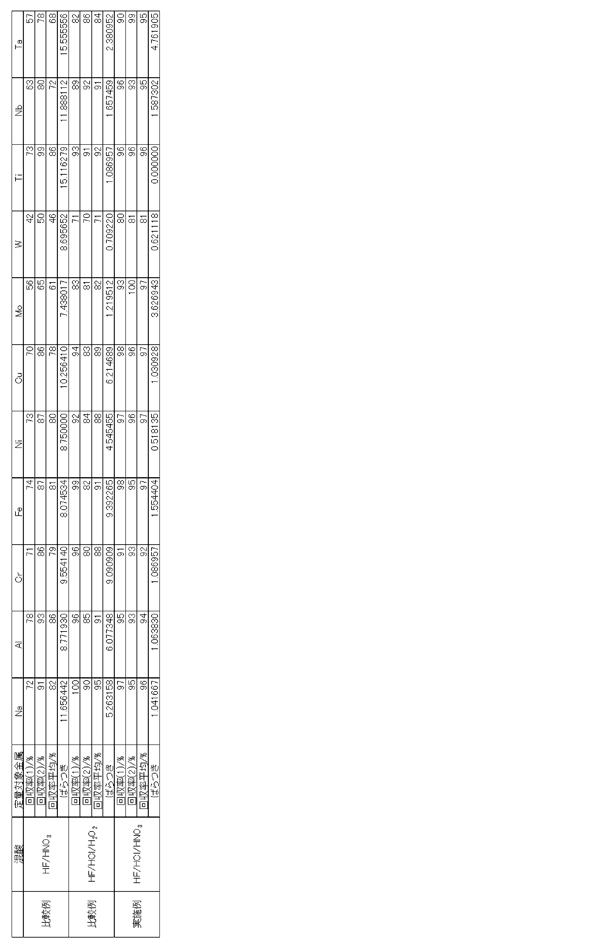
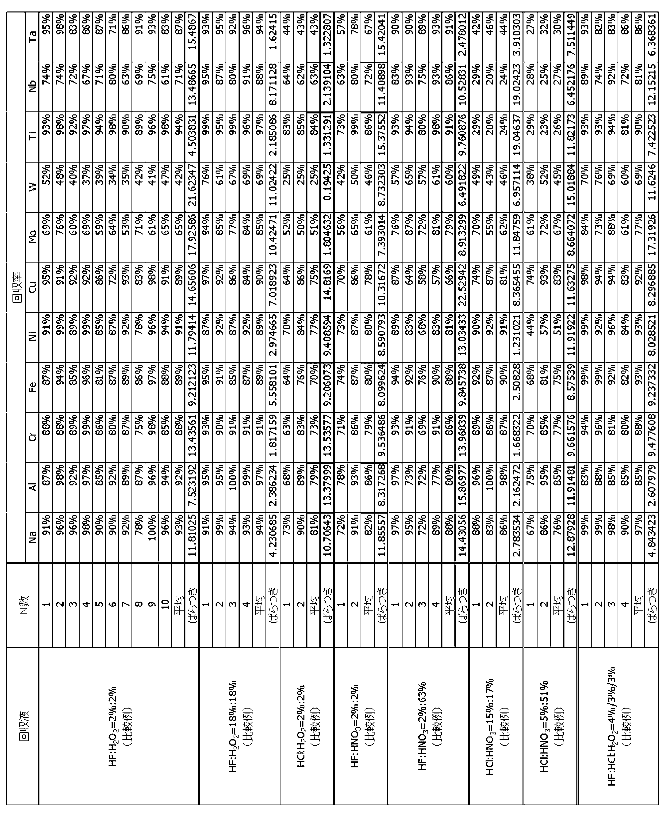
下記表2、3に示す各種混酸を用いて、下記表2、3に示す各種金属成分について、上記1.と同様の方法で既知濃度の金属汚染処理を施したサセプタを上記2.~4.の工程に付すことを下記表2、3に示す回数行って得られた定量分析結果(回収率、回収率の平均およびばらつき)を、表2、3に示す。下記表2、3に示す混酸は、酸成分が表中に示す酸からなり、それぞれの酸を表中に示す濃度で含む水溶液である。
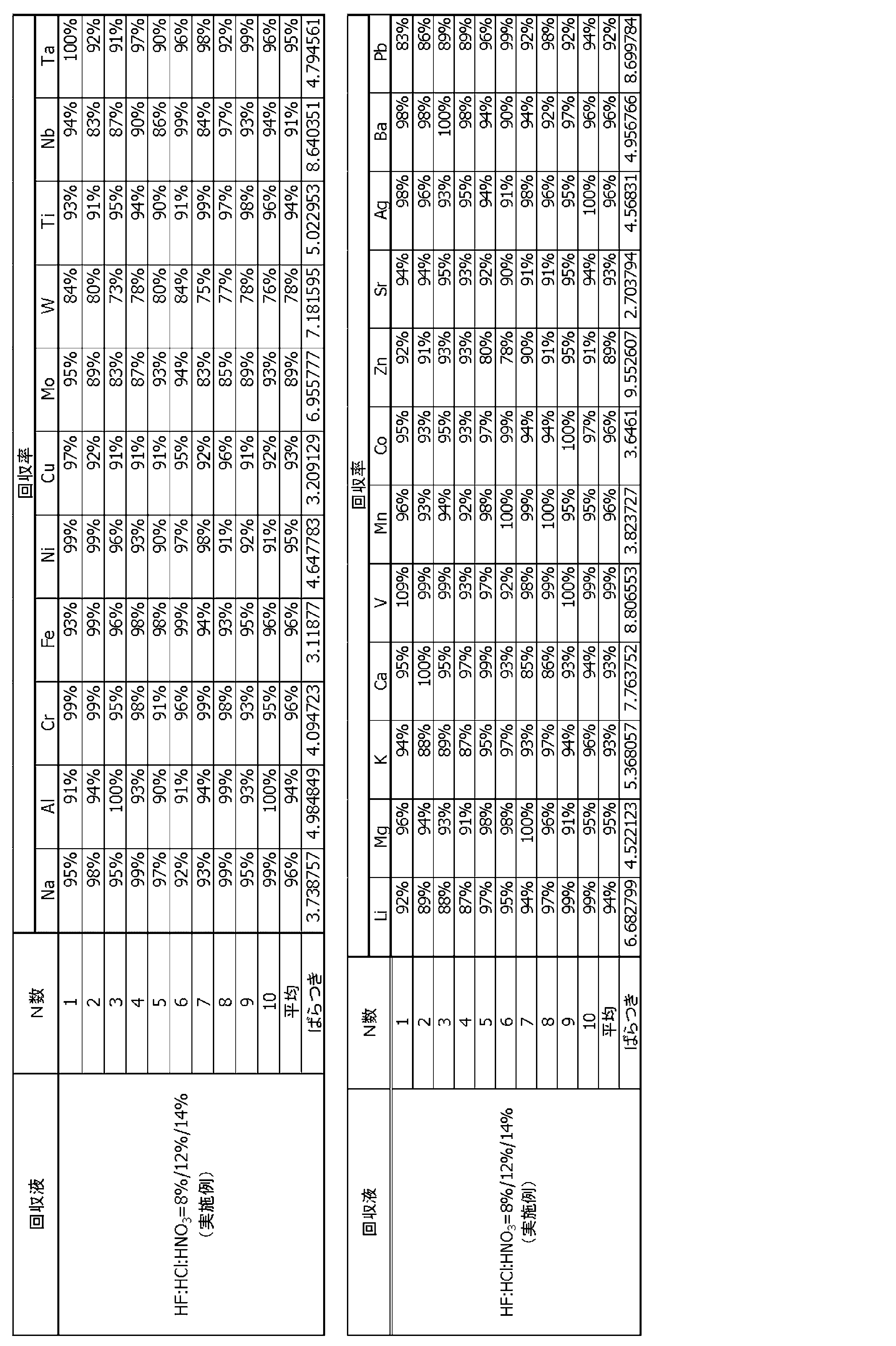
また、実施例で定量分析に用いたICP-MSは、高感度な定量分析が可能な装置である。ICP-MSによれば、わずかな金属汚染であっても検出し定量することができる。
以上の結果から、実施例において、炭化珪素系部材の清浄度を高精度に分析可能であったことが確認できる。

Claims (8)
- 炭化珪素表面を有する部材の清浄度評価方法であって、
前記炭化珪素表面を、フッ化水素酸、塩酸および硝酸の混酸と接触させること、
前記炭化珪素表面と接触させた混酸を加熱により濃縮すること、
前記濃縮により得られた濃縮液を希釈して得られた試料溶液を、誘導結合プラズマ質量分析計による金属成分の定量分析に付すこと、および、
前記定量分析により得られた金属成分定量結果に基づき、前記炭化珪素表面を有する部材の清浄度を評価すること、
を含む、前記清浄度評価方法。 - 前記混酸において、フッ化水素酸の濃度は5~15質量%の範囲であり、塩酸の濃度は5~15質量%の範囲であり、かつ硝酸の濃度は5~15質量%の範囲である、請求項1に記載の清浄度評価方法。
- 前記試料溶液を、前記濃縮により得られた濃縮液をフッ化水素酸および過酸化水素を添加して希釈することにより調製する、請求項1または2に記載の清浄度評価方法。
- 前記炭化珪素表面を有する部材は、シリコンウェーハ製造用部材である請求項1~3のいずれか1項に記載の清浄度評価方法。
- 前記シリコンウェーハ製造用部材は、サセプタである請求項4に記載の清浄度評価方法。
- 炭化珪素表面を有する部材の洗浄条件決定方法であって、
炭化珪素表面を有する部材の前記炭化珪素表面を、候補洗浄条件下で洗浄すること、
前記洗浄後の炭化珪素表面を有する部材の清浄度を、請求項1~5のいずれか1項に記載の方法により評価すること、および、
前記評価の結果、清浄度が許容レベル以内と判定された候補洗浄条件を、シリコンウェーハの実製造工程における炭化珪素表面を有する部材の洗浄条件として決定すること、
を含む、前記洗浄条件決定方法。 - シリコンウェーハの製造方法であって、
請求項6に記載の方法により洗浄条件を決定すること、
決定された洗浄条件下で炭化珪素表面を有するシリコンウェーハ製造用部材を洗浄すること、および、
前記洗浄後のシリコンウェーハ製造用部材を用いる工程を含む製造工程を経て、シリコンウェーハを製造すること、
を含む、前記シリコンウェーハの製造方法。 - シリコンウェーハの製造方法であって、
炭化珪素表面を有するシリコンウェーハ製造用部材の清浄度を、請求項1~5のいずれか1項に記載の方法により評価すること、
前記評価の結果、清浄度が許容レベル以内であると判定されたシリコンウェーハ製造用部材を用いる工程を含む製造工程を経て、シリコンウェーハを製造すること、
を含む、前記シリコンウェーハの製造方法。
Priority Applications (5)
| Application Number | Priority Date | Filing Date | Title |
|---|---|---|---|
| KR1020187026228A KR102136733B1 (ko) | 2016-03-28 | 2017-02-28 | 청정도 평가 방법, 세정 조건 결정 방법 및, 실리콘 웨이퍼의 제조 방법 |
| CN201780016301.5A CN109313162B (zh) | 2016-03-28 | 2017-02-28 | 清洁度评价方法、清洗条件决定方法、和硅晶圆的制造方法 |
| US16/087,879 US11118285B2 (en) | 2016-03-28 | 2017-02-28 | Method of evaluating cleanliness, method of determining cleaning condition, and method of manufacturing silicon wafer |
| DE112017001570.7T DE112017001570B4 (de) | 2016-03-28 | 2017-02-28 | Verfahren zur Bewertung der Reinheit, Verfahren zur Bestimmung des Reinigungszustandes und Verfahren zur Herstellung von Siliciumwafern |
| US17/392,652 US11920257B2 (en) | 2016-03-28 | 2021-08-03 | Method of evaluating cleanliness, method of determining cleaning condition, and method of manufacturing silicon wafer |
Applications Claiming Priority (2)
| Application Number | Priority Date | Filing Date | Title |
|---|---|---|---|
| JP2016-064071 | 2016-03-28 | ||
| JP2016064071A JP6269709B2 (ja) | 2016-03-28 | 2016-03-28 | 清浄度評価方法、洗浄条件決定方法、およびシリコンウェーハの製造方法 |
Related Child Applications (2)
| Application Number | Title | Priority Date | Filing Date |
|---|---|---|---|
| US16/087,879 A-371-Of-International US11118285B2 (en) | 2016-03-28 | 2017-02-28 | Method of evaluating cleanliness, method of determining cleaning condition, and method of manufacturing silicon wafer |
| US17/392,652 Division US11920257B2 (en) | 2016-03-28 | 2021-08-03 | Method of evaluating cleanliness, method of determining cleaning condition, and method of manufacturing silicon wafer |
Publications (1)
| Publication Number | Publication Date |
|---|---|
| WO2017169458A1 true WO2017169458A1 (ja) | 2017-10-05 |
Family
ID=59962978
Family Applications (1)
| Application Number | Title | Priority Date | Filing Date |
|---|---|---|---|
| PCT/JP2017/007749 Ceased WO2017169458A1 (ja) | 2016-03-28 | 2017-02-28 | 清浄度評価方法、洗浄条件決定方法、およびシリコンウェーハの製造方法 |
Country Status (7)
| Country | Link |
|---|---|
| US (2) | US11118285B2 (ja) |
| JP (1) | JP6269709B2 (ja) |
| KR (1) | KR102136733B1 (ja) |
| CN (1) | CN109313162B (ja) |
| DE (1) | DE112017001570B4 (ja) |
| TW (1) | TWI635275B (ja) |
| WO (1) | WO2017169458A1 (ja) |
Cited By (1)
| Publication number | Priority date | Publication date | Assignee | Title |
|---|---|---|---|---|
| CN109655154A (zh) * | 2018-12-29 | 2019-04-19 | 重庆工商大学 | 一种基于高光谱稀疏解混装置 |
Families Citing this family (4)
| Publication number | Priority date | Publication date | Assignee | Title |
|---|---|---|---|---|
| CN111879542B (zh) * | 2020-07-30 | 2023-02-28 | 徐州鑫晶半导体科技有限公司 | 清洗机清洗能力的检测方法和检测装置 |
| KR102339658B1 (ko) * | 2021-03-25 | 2021-12-14 | 주식회사 피피엠아이 | 모발시료 내 중금속 및 영양미네랄 분석방법 |
| CN115144459A (zh) * | 2022-06-23 | 2022-10-04 | 东莞市天域半导体科技有限公司 | 一种检测碳化硅外延晶片表面痕量金属的方法 |
| CN117855025A (zh) * | 2022-09-30 | 2024-04-09 | 比亚迪股份有限公司 | 碳化硅外延片及其制备方法 |
Citations (4)
| Publication number | Priority date | Publication date | Assignee | Title |
|---|---|---|---|---|
| JPH1074481A (ja) * | 1996-08-30 | 1998-03-17 | Tokyo Electron Ltd | イオンエネルギー測定方法及び装置 |
| JP2000335992A (ja) * | 1999-05-31 | 2000-12-05 | Mitsubishi Materials Silicon Corp | シリコン単結晶育成装置内のガスの測定方法及びその装置 |
| JP2002040009A (ja) * | 2000-07-28 | 2002-02-06 | Mitsubishi Materials Silicon Corp | シリコン基板中の微量不純物分析方法 |
| JP2012132779A (ja) * | 2010-12-21 | 2012-07-12 | Sumco Corp | シリコン試料の分析方法 |
Family Cites Families (18)
| Publication number | Priority date | Publication date | Assignee | Title |
|---|---|---|---|---|
| JPH0878375A (ja) * | 1994-08-31 | 1996-03-22 | Sumitomo Metal Ind Ltd | 炭化珪素製治具の洗浄方法 |
| JPH08288248A (ja) | 1995-04-14 | 1996-11-01 | Watanabe Shoko:Kk | 接液部材 |
| KR100271762B1 (ko) * | 1997-12-05 | 2000-12-01 | 윤종용 | 반도체 제조설비 시료 용융용 케미컬 및 이를 이용한 불순물 분석방법 |
| JP4188473B2 (ja) | 1998-12-08 | 2008-11-26 | 株式会社ブリヂストン | 炭化ケイ素焼結体の湿式洗浄方法 |
| JP2000332072A (ja) | 1999-05-20 | 2000-11-30 | Canon Inc | 半導体基板の表面分析方法 |
| JP2001250785A (ja) | 2000-03-06 | 2001-09-14 | Toshiba Ceramics Co Ltd | 炭化ケイ素が被覆された半導体熱処理用部材の洗浄方法 |
| WO2002015255A1 (en) * | 2000-08-11 | 2002-02-21 | Chem Trace Corporation | System and method for cleaning semiconductor fabrication equipment parts |
| JP2005047753A (ja) * | 2003-07-29 | 2005-02-24 | Tadahiro Omi | 炭化珪素製品、その製造方法、及び、炭化珪素製品の洗浄方法 |
| US7291286B2 (en) * | 2004-12-23 | 2007-11-06 | Lam Research Corporation | Methods for removing black silicon and black silicon carbide from surfaces of silicon and silicon carbide electrodes for plasma processing apparatuses |
| JP5028238B2 (ja) | 2007-12-04 | 2012-09-19 | 野村マイクロ・サイエンス株式会社 | 金属汚染物質測定方法及び装置 |
| JP5033168B2 (ja) | 2009-09-29 | 2012-09-26 | 忠弘 大見 | 炭化珪素製品、その製造方法、及び、炭化珪素製品の洗浄方法 |
| CN102079523A (zh) | 2010-12-15 | 2011-06-01 | 东海晶澳太阳能科技有限公司 | 一种大颗粒冶金硅料金属杂质的去除方法 |
| JP5770049B2 (ja) * | 2011-08-29 | 2015-08-26 | 株式会社アナック | フッ酸含有処理液の再生方法及び再生装置 |
| CN102602935B (zh) | 2012-03-05 | 2014-03-12 | 矽明科技股份有限公司 | 一种高钙除磷的硅的清洗方法 |
| CN104280382B (zh) | 2013-10-31 | 2016-11-02 | 东旭集团有限公司 | 一种检测碳化硅中氧化铁含量的方法 |
| KR101523943B1 (ko) | 2013-12-24 | 2015-06-01 | 주식회사 엘지실트론 | 웨이퍼 제조 공정의 오염 분석 방법 |
| CN103681246B (zh) * | 2013-12-30 | 2017-10-17 | 国家电网公司 | 一种SiC材料清洗方法 |
| JP6142128B2 (ja) | 2014-09-25 | 2017-06-07 | 株式会社大都技研 | 遊技台 |
-
2016
- 2016-03-28 JP JP2016064071A patent/JP6269709B2/ja active Active
-
2017
- 2017-02-24 TW TW106106372A patent/TWI635275B/zh active
- 2017-02-28 US US16/087,879 patent/US11118285B2/en active Active
- 2017-02-28 CN CN201780016301.5A patent/CN109313162B/zh active Active
- 2017-02-28 KR KR1020187026228A patent/KR102136733B1/ko active Active
- 2017-02-28 WO PCT/JP2017/007749 patent/WO2017169458A1/ja not_active Ceased
- 2017-02-28 DE DE112017001570.7T patent/DE112017001570B4/de active Active
-
2021
- 2021-08-03 US US17/392,652 patent/US11920257B2/en active Active
Patent Citations (4)
| Publication number | Priority date | Publication date | Assignee | Title |
|---|---|---|---|---|
| JPH1074481A (ja) * | 1996-08-30 | 1998-03-17 | Tokyo Electron Ltd | イオンエネルギー測定方法及び装置 |
| JP2000335992A (ja) * | 1999-05-31 | 2000-12-05 | Mitsubishi Materials Silicon Corp | シリコン単結晶育成装置内のガスの測定方法及びその装置 |
| JP2002040009A (ja) * | 2000-07-28 | 2002-02-06 | Mitsubishi Materials Silicon Corp | シリコン基板中の微量不純物分析方法 |
| JP2012132779A (ja) * | 2010-12-21 | 2012-07-12 | Sumco Corp | シリコン試料の分析方法 |
Cited By (2)
| Publication number | Priority date | Publication date | Assignee | Title |
|---|---|---|---|---|
| CN109655154A (zh) * | 2018-12-29 | 2019-04-19 | 重庆工商大学 | 一种基于高光谱稀疏解混装置 |
| CN109655154B (zh) * | 2018-12-29 | 2020-11-10 | 重庆工商大学 | 一种基于高光谱稀疏解混装置 |
Also Published As
| Publication number | Publication date |
|---|---|
| KR102136733B1 (ko) | 2020-07-22 |
| CN109313162B (zh) | 2021-10-29 |
| US11920257B2 (en) | 2024-03-05 |
| US11118285B2 (en) | 2021-09-14 |
| TW201800750A (zh) | 2018-01-01 |
| KR20180114120A (ko) | 2018-10-17 |
| US20210363660A1 (en) | 2021-11-25 |
| TWI635275B (zh) | 2018-09-11 |
| DE112017001570B4 (de) | 2026-04-30 |
| JP2017181092A (ja) | 2017-10-05 |
| DE112017001570T5 (de) | 2018-12-13 |
| CN109313162A (zh) | 2019-02-05 |
| US20190106810A1 (en) | 2019-04-11 |
| JP6269709B2 (ja) | 2018-01-31 |
Similar Documents
| Publication | Publication Date | Title |
|---|---|---|
| US11920257B2 (en) | Method of evaluating cleanliness, method of determining cleaning condition, and method of manufacturing silicon wafer | |
| JP5720297B2 (ja) | シリコンウェーハの金属汚染分析方法 | |
| TWI421965B (zh) | 處理半導體製程元件之方法及其形成之元件 | |
| JP2013108759A (ja) | 半導体ウェハプロセス用ふっ酸溶液の不純物分析方法および該ふっ酸溶液の交換時期の管理方法 | |
| US20040235231A1 (en) | Method for treating semiconductor processing components and components formed thereby | |
| JP6696729B2 (ja) | 半導体基板の評価方法及び半導体基板の製造方法 | |
| JP2004012315A (ja) | 炭化ケイ素材または窒化ケイ素材の不純物濃度分布測定方法ならびにセラミックスの不純物濃度分布測定方法 | |
| JP6819883B2 (ja) | シリコンウェーハの金属不純物分析方法 | |
| CN110223927A (zh) | 硅晶片的金属污染分析方法 | |
| JP6063616B2 (ja) | シリコン試料の分析方法 | |
| JPH10223713A (ja) | 熱処理評価用ウェ−ハおよびこれを用いた熱処理評価方法 | |
| US11424129B2 (en) | Method of etching boron-doped p-type silicon wafer, method of evaluating metal contamination of boron-doped p-type silicon wafer and method of manufacturing boron-doped p-type silicon wafer | |
| JP2009294091A (ja) | シリコンウェーハ中の汚染物の分析方法 | |
| JP2000332072A (ja) | 半導体基板の表面分析方法 | |
| Ichikawa et al. | Analysis of metallic impurities in Si wafers using fully automated VPD ICP-MS | |
| KR100999358B1 (ko) | 실리콘 웨이퍼의 금속 불순물 평가 방법 | |
| JP7131513B2 (ja) | シリコン試料の前処理方法、シリコン試料の金属汚染評価方法、単結晶シリコンインゴット育成工程の評価方法、単結晶シリコンインゴットの製造方法およびシリコンウェーハの製造方法 | |
| KR101312545B1 (ko) | 표준 웨이퍼 및 그의 생산 방법 | |
| CN120369417A (zh) | 一种pe袋内的金属离子含量的检测方法 | |
| JPH11326280A (ja) | 微量金属の分析方法 | |
| JP2009519449A (ja) | 石英ガラス部材の表面充填量の測定方法 | |
| JP2010114282A (ja) | 半導体基板の金属汚染評価方法 |
Legal Events
| Date | Code | Title | Description |
|---|---|---|---|
| ENP | Entry into the national phase |
Ref document number: 20187026228 Country of ref document: KR Kind code of ref document: A |
|
| WWE | Wipo information: entry into national phase |
Ref document number: 1020187026228 Country of ref document: KR |
|
| 121 | Ep: the epo has been informed by wipo that ep was designated in this application |
Ref document number: 17774003 Country of ref document: EP Kind code of ref document: A1 |
|
| 122 | Ep: pct application non-entry in european phase |
Ref document number: 17774003 Country of ref document: EP Kind code of ref document: A1 |