WO2016208141A1 - 半導体素子の検査装置および検査方法 - Google Patents
半導体素子の検査装置および検査方法 Download PDFInfo
- Publication number
- WO2016208141A1 WO2016208141A1 PCT/JP2016/002793 JP2016002793W WO2016208141A1 WO 2016208141 A1 WO2016208141 A1 WO 2016208141A1 JP 2016002793 W JP2016002793 W JP 2016002793W WO 2016208141 A1 WO2016208141 A1 WO 2016208141A1
- Authority
- WO
- WIPO (PCT)
- Prior art keywords
- switch
- turned
- rectifying
- coil
- semiconductor element
- Prior art date
- Legal status (The legal status is an assumption and is not a legal conclusion. Google has not performed a legal analysis and makes no representation as to the accuracy of the status listed.)
- Ceased
Links
Images



Classifications
-
- G—PHYSICS
- G01—MEASURING; TESTING
- G01R—MEASURING ELECTRIC VARIABLES; MEASURING MAGNETIC VARIABLES
- G01R31/00—Arrangements for testing electric properties; Arrangements for locating electric faults; Arrangements for electrical testing characterised by what is being tested not provided for elsewhere
- G01R31/26—Testing of individual semiconductor devices
- G01R31/2601—Apparatus or methods therefor
-
- G—PHYSICS
- G01—MEASURING; TESTING
- G01R—MEASURING ELECTRIC VARIABLES; MEASURING MAGNETIC VARIABLES
- G01R31/00—Arrangements for testing electric properties; Arrangements for locating electric faults; Arrangements for electrical testing characterised by what is being tested not provided for elsewhere
- G01R31/26—Testing of individual semiconductor devices
- G01R31/2607—Circuits therefor
- G01R31/2632—Circuits therefor for testing diodes
- G01R31/2633—Circuits therefor for testing diodes for measuring switching properties thereof
-
- G—PHYSICS
- G01—MEASURING; TESTING
- G01R—MEASURING ELECTRIC VARIABLES; MEASURING MAGNETIC VARIABLES
- G01R31/00—Arrangements for testing electric properties; Arrangements for locating electric faults; Arrangements for electrical testing characterised by what is being tested not provided for elsewhere
- G01R31/28—Testing of electronic circuits, e.g. by signal tracer
- G01R31/2851—Testing of integrated circuits [IC]
- G01R31/2886—Features relating to contacting the IC under test, e.g. probe heads; chucks
Definitions
- the present disclosure relates to an inspection apparatus and an inspection method for a semiconductor element having a diode element.
- Patent Document 1 Conventionally, as an inspection apparatus of this type, for example, the following inspection circuit has been proposed in Patent Document 1. That is, in this inspection circuit, a switch, a coil, and a semiconductor element are arranged in series with respect to the power supply, and when the switch and the switching element that constitutes the semiconductor element are turned off, a loop path is formed with the coil. A diode element is arranged. The cathode electrode of the diode element is connected to the positive electrode side of the power source.
- a semiconductor element or a diode element can be used as an element to be inspected (DUT: Device Under Test).
- DUT Device Under Test
- the diode element is a DUT
- the switch is repeatedly turned on and off in order to check the recovery characteristics of the DUT, a return current flows through a loop path including the coil and the DUT when the switch is turned off. Thereafter, when the switch is turned on, a recovery current flows through the DUT, and when the switch is turned off, a return current flows through the DUT again.
- the DUT Since the return period after recovery is longer than the return period before recovery, the DUT generates more heat when the return current after recovery flows than when the return current before recovery flows. For this reason, the DUT may be damaged and destroyed by the reflux current after recovery.
- the current concentrates at the location where the DUT is destroyed, and a large current flows through the inspection equipment such as the probe and the stage arranged in contact with the electrodes on the surface of the DUT. Therefore, when the DUT is destroyed by the reflux current after recovery, damage to the inspection equipment is promoted.
- the present disclosure has been made in view of the above points, and an object of the present disclosure is to provide a semiconductor element inspection apparatus and inspection method that reduce damage to inspection equipment when a DUT has a diode element.
- a semiconductor device inspection apparatus includes a first switch having a switching element, a coil, and a second switch connected in series to a power source, and a coil when the switching element is turned off.
- a semiconductor element as a test object having a diode element that is arranged to form a loop path together with the second switch and has a cathode electrode connected to the positive electrode side of the power supply, and a loop path different from the loop path including the semiconductor element
- the inspection apparatus since the loop path different from the loop path including the semiconductor element is configured by the coil, the first rectifying element, and the second rectifying element, it is possible to suppress the return current from flowing into the semiconductor element. , Damage to the inspection equipment can be reduced.
- a semiconductor element inspection method for inspecting a semiconductor element as an inspection object having a diode element includes connecting a first switch having a switching element, a coil, and a second switch to a power supply in series.
- the semiconductor element is arranged to form a loop path together with the coil and the second switch when the switching element is turned off, the cathode electrode of the diode element is connected to the positive side of the power source, the first rectifying element, and
- a second rectifying element connected in series with the first rectifying element and having a rectifying action opposite to that of the first rectifying element is disposed so as to constitute a loop path different from the loop path including the semiconductor element together with the coil; This includes inspecting the semiconductor element by repeatedly turning on and off the switching element.
- the coil, the first rectifying element, and the second rectifying element are arranged so as to form a loop path different from the loop path including the semiconductor element, the return current flows into the semiconductor element. This can be suppressed and damage to the inspection equipment can be reduced.
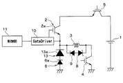
- FIG. 1 is a diagram illustrating a configuration of an inspection apparatus according to the first embodiment of the present disclosure.
- FIG. 2 is a diagram showing the relationship between the state of the first switch and the current flowing through the DUT in the conventional inspection apparatus
- FIG. 3 is a diagram showing the relationship between the state of the first switch and the current flowing through the DUT in the inspection apparatus shown in FIG.
- FIG. 4 is a diagram illustrating a first modification of the first embodiment.
- FIG. 5 is a diagram showing the relationship between the state of the second switch and the current flowing through the DUT in the second modification of the first embodiment.
- FIG. 6 is a diagram illustrating a configuration of an inspection apparatus according to the second embodiment of the present disclosure.
- FIG. 7 is a diagram illustrating a configuration of an inspection apparatus according to the third embodiment of the present disclosure.
- FIG. 8 is a diagram illustrating a configuration of an inspection apparatus according to the fourth embodiment of the present disclosure.
- the semiconductor element inspection apparatus performs a recovery inspection of a semiconductor element using a power supply 1.
- the inspection apparatus includes a power source 1, a first switch 2, a coil 3, a second switch 4, a protective switch 5, a DUT 6, an ammeter 7, and a first rectifying element. 8, a second rectifying element 9, a gate driver 10, and a control unit 11.
- a protection switch 5, a second switch 4, a coil 3, and a first switch 2 are connected in series to a power source 1.
- the first switch 2 switches the path of the current flowing through the coil 3, and has a switching element 2a.
- the switching element 2a is composed of an N-channel IGBT (insulated gate bipolar transistor) element having a gate electrode, a collector electrode, and an emitter electrode.
- the gate electrode of the switching element 2 a is connected to the gate driver 10, and the gate driver 10 is connected to the control unit 11.
- the gate driver 10 changes the gate voltage of the switching element 2a in accordance with a signal input from the control unit 11, and switches the first switch 2 on and off.
- the gate driver 10 is connected to the negative electrode (ground) of the power supply 1.
- the control unit 11 repeatedly turns on and off the switching element 2 a through the gate driver 10.
- the coil 3 assumes an inductance component of the L load.
- a reflux current is passed through the DUT 6.
- the second switch 4 switches the path of the current flowing through the coil 3 when the first switch 2 is turned off.
- the N-channel IGBT element having a gate electrode, a collector electrode, and an emitter electrode Consists of.
- the gate electrode of the second switch 4 is connected to a gate driver (not shown), and this gate driver is connected to the control unit 11.
- the controller 11 switches the second switch 4 on and off according to the situation through the gate driver.
- the protection switch 5 is for cutting off the current supplied from the power source 1 to the second switch 4 and the like when the DUT 6 is destroyed, and suppressing damage to the inspection equipment. It is composed of an N channel type IGBT element having an electrode, a collector electrode, and an emitter electrode.
- the gate electrode of the protection switch 5 is connected to a gate driver (not shown), and this gate driver is connected to the control unit 11.
- this gate driver is connected to the control unit 11.
- the positive electrode of the power source 1 is connected to the collector electrode of the protective switch 5.
- the emitter electrode of the protection switch 5 is connected to the collector electrode of the second switch 4.
- the emitter electrode of the second switch 4 is connected to one end of the coil 3.
- the other end of the coil 3 is connected to the collector electrode of the switching element 2 a included in the first switch 2.
- the emitter electrode of the switching element 2a is connected to the ground.
- the DUT 6 and the ammeter 7 are arranged so as to form a loop path P1 together with the coil 3 and the second switch 4 when the first switch 2 is turned off.
- the DUT 6 is connected in series with the ammeter 7.
- the DUT 6 is an inspection target in the present embodiment, and corresponds to the semiconductor element of the present disclosure.
- the DUT 6 includes a diode element 6a, and the diode element 6a is formed of a vertical FWD (free wheel diode) element.
- One electrode of the diode element 6a is in contact with a probe (not shown), and the other electrode is in contact with a wiring provided on a stage (not shown).
- the ammeter 7 measures the current flowing through the DUT 6 in order to detect the destruction of the DUT 6.
- the method described in Patent Document 1 can be used as a method for detecting destruction.
- the ammeter 7 is connected to the control unit 11 by a wiring (not shown), and the control unit 11 detects an overcurrent based on the output of the ammeter 7 and determines whether or not the DUT 6 is destroyed.
- the ammeter 7 measures the current flowing through the DUT 6, and the control unit 11 detects the destruction of the DUT 6 based on the output of the ammeter 7. Therefore, the ammeter 7 and the control unit 11 correspond to a destruction detection unit of the present disclosure.
- the cathode electrode of the diode element 6 a included in the DUT 6 is connected to the positive electrode side of the power source 1 via the ammeter 7 and the protection switch 5.
- the anode electrode of the diode element 6 a is connected to the wiring between the first switch 2 and the coil 3.
- the first rectifying element 8 and the second rectifying element 9 constitute a loop path P2 different from the loop path P1 including the DUT 6 together with the coil 3.
- the second rectifying element 9 is connected in series with the first rectifying element 8 so as to have a rectifying action opposite to that of the first rectifying element 8.
- the first rectifying element 8 is for suppressing the current flowing through the coil 3 from traveling on the loop path P2 when the second switch 4 is turned on.
- the first rectifying element 8 is configured by a Zener diode element. Is done.
- the first rectifying element 8 is connected so as to have a rectifying action in the direction opposite to the current flowing by the counter electromotive force of the coil 3 when the second switch 4 is turned off.
- the second rectifying element 9 is for suppressing the current flowing through the second switch 4 from being supplied to the first switch 2 not via the coil 3 but via the first rectifying element 8, and is constituted by an FWD element. Is done.
- the control unit 11 operates each switch according to the situation, and includes a well-known microcomputer including a CPU, a ROM, a RAM, an I / O, and the like.
- the control unit 11 performs processing such as various calculations in accordance with a program stored in a ROM or the like, and performs a recovery inspection of the DUT 6.
- control unit 11 alternately repeats the operation of turning on the first switch 2 and the operation of turning off the first switch 2 twice. Further, the control unit 11 turns on the second switch 4 and turns on the first switch for the second time after turning on the first switch 2 for the first time until turning on the first switch 2 for the second time. After turning on 2, the second switch 4 is turned off before turning the first switch 2 off for the second time.
- control unit 11 turns on the protection switch 5 before turning off the first switch 2 for the first time, and turns off the second switch 4 when the destruction of the DUT 6 is detected based on the signal from the ammeter 7. After that, the first switch 2 and the protection switch 5 are turned off.
- the above is the configuration of the semiconductor element inspection apparatus in this embodiment. Next, a semiconductor element inspection method using the above inspection apparatus will be described in comparison with a conventional inspection apparatus.
- the control unit 11 inputs a pulsed drive signal having a predetermined amplitude and frequency through the gate driver 10 to the gate electrode of the switching element 2a, and alternately turns on and off the switching element 2a, and the current flowing through the DUT 6 And change the voltage. Thereby, the characteristic inspection of the DUT 6 is performed.
- the controller 11 turns on the switching element 2a at time T1, and turns off the switching element 2a at time T2. Thereafter, the switching element 2a is turned on at time T3, and the switching element 2a is turned off at time T4.
- Vg1 and Vg2 are high-level or low-level gate signals applied to the switching element 2a and the second switch 4, respectively.
- Vka is a voltage applied to both ends of the diode element 6a.
- the current (forward current) I flowing through the DUT 6 gradually increases and the return current flows through the loop path P1.
- the switching element 2a is turned on at time T3, as indicated by the regions R1 and R3, the current I flowing through the DUT 6 gradually decreases and a recovery current (reverse current) is generated.
- the first rectifying element 8, and the second rectifying element 9 after the recovery of the DUT 6 is completed, when the switching element 2 a is turned off at time T 4, FIG. As indicated by the region R2, the return current flows through the DUT 6 included in the loop path P1.
- the DUT 6 Since the return period after recovery is longer than the return period before recovery, the DUT 6 generates more heat when the return current after recovery flows than when the return current before recovery flows. Therefore, the DUT 6 may be damaged and destroyed by the reflux current after recovery.
- the first rectifying element 8 and the second rectifying element 9 are arranged so as to constitute the loop path P2 together with the coil 3.
- the 2nd switch 4 is arrange
- control unit 11 turns on the second switch 4 before the time point T1, and turns off the second switch 4 after the time point T3 and before the time point T4. More specifically, the control unit 11 turns off the second switch after the completion of the recovery operation of the DUT 6 and before the time point T4 when the reflux operation is started. For this reason, when the switching element 2a is turned off at time T4, the return current flows through the loop path P2 instead of the loop path P1, and no return current flowing through the DUT 6 is generated as indicated by a region R4 in FIG.
- the control unit 11 turns off the protection switch 5 in order to protect the power supply 1 when the destruction of the DUT 6 is detected based on the signal from the ammeter 7.
- the maximum value of the forward voltage of the diode element 6a when the reflux current is generated is Vfp1.
- the maximum value Vfp1 is a peak value of the voltage Vka that increases in the forward direction due to carrier accumulation delay after the first switch 2 is turned off and a return current is generated.
- Vmax1 Vfp1 + Von. This is a reverse bias at the start of recirculation, and it is necessary that Vz> Vfp1 + Von in order to allow the recirculation current to flow through the loop path P2 only when the second switch 4 is turned off.
- the loop path P2 becomes difficult to flow through the return current, and thus does not serve as a return path.
- Vz ⁇ Vbr ⁇ Vcc needs to be satisfied.
- the coil 3, the first rectifying element 8, and the second rectifying element 9 are arranged so as to constitute a loop path P2 different from the loop path P1 including the DUT 6. , It is possible to suppress the return current from flowing into the DUT 6 and reduce the damage to the DUT 6. Thereby, damage to the inspection device can be reduced. In addition, even when the DUT 6 is destroyed in the recovery operation, it is possible to reduce damage to the elements and inspection equipment due to the reflux current.
- the smoothing capacitor 12 may be arrange
- the second switch 4 is turned off at a time point after the time point T3 and before the time point T4 regardless of whether or not the DUT 6 is broken.
- the DUT 6 is broken by the output from the ammeter 7. Only when it is detected, the second switch 4 may be turned off at this time.
- control unit 11 detects the destruction of the DUT 6 using a predetermined value of the reverse current flowing through the DUT 6 as a threshold value, and this threshold value is larger than the peak value of the reverse current when the DUT 6 is not destroyed. Is set to
- the current threshold Ith for detecting the destruction of the DUT 6 includes a recovery current peak value I1 when the DUT 6 is not destroyed and a recovery current when the DUT 6 is destroyed, as shown in FIG. It is set between the peak value I2.
- the control unit 11 determines that the DUT 6 has been destroyed.
- the second switch 4 when the destruction of the DUT 6 is not detected, the second switch 4 is turned on from before the time T1 to after the time T4. As a result, the reflux current after time T4 flows through the loop path P1 including DUT6. When the DUT 6 is destroyed by the recovery current, the second switch 4 is turned off after the time T3 and before the time T4, as shown by the dotted line in FIG. As a result, as indicated by the one-dot chain line in FIG. 5, the reflux current does not flow into the DUT 6.
- the control unit 11 turns off the first switch 2 and the protection switch 5 when the ammeter 7 detects the destruction of the DUT 6. At this time, if the protection switch 5 is turned off before the second switch 4 is turned off, the return current flows through the loop path P1 after the protection switch 5 is turned off, and the damage of the inspection device is promoted. On the other hand, in this modification, the second switch 4 is turned off before the first switch 2 and the protection switch 5 are turned off after the destruction of the DUT 6 is detected. Thereby, it can suppress that a return current flows through the loop path
- the second switch 4 is turned off at a time point between the time point T3 and the time point T4, and the return current after the time point T4 is switched by switching the route of the return current.
- the operation of the DUT 6 when flowing can also be inspected.
- the protection element 13 is arranged so as to form a loop path together with the coil 3, the second switch 4, the DUT 6, and the ammeter 7 when the first switch 2 is turned off. ing.
- the protection element 13 includes a protection diode element 13a having a greater breakdown resistance than the DUT 6.
- the protective diode element 13a is composed of an FWD element, and is disposed so as to have a rectifying action in the same direction as the diode element 6a. Specifically, the cathode electrode of the protective diode element 13a is connected to the anode electrode of the diode element 6a. The anode electrode of the protection diode element 13a is connected to the collector electrode of the switching element 2a. One end of the coil 3 is connected to the wiring between the protection diode element 13a and the switching element 2a.
- Vz> Vfp1 + Vfp2 + Von is established in order to allow the reflux current to flow through the loop path P2 only when the second switch 4 is turned off.
- Vfp2 is the maximum value of the forward voltage of the protective diode element 13a when the return current is generated.
- the present embodiment having such a configuration, even if the DUT 6 is destroyed by the recovery current, it is possible to suppress the absolute value of the short-circuit current flowing through the DUT 6 from being sharply increased by the protective diode element 13a. That is, it is possible to suppress a large current from flowing through the DUT 6. For this reason, it is possible to further reduce damage to inspection equipment such as probes and stages.
- the protective element 13 is arranged as described above, but the position of the DUT 6 and the position of the protective element 13 may be interchanged. That is, the cathode electrode of the protective diode element 13a may be connected to the ammeter 7, the anode electrode may be connected to the cathode electrode of the diode element 6a, and the anode electrode of the diode element 6a may be connected to the collector electrode of the switching element 2a.
- the second embodiment which is the lower arm drive (that is, the low side drive), is the upper arm drive (that is, the high side drive), and the other aspects are the same as those of the second embodiment. Only portions different from the embodiment will be described.
- the positions of the elements constituting the loop path P1 and the first switch 2 are interchanged. That is, as shown in FIG. 7, the emitter electrode of the protection switch 5 is connected to the collector electrode of the switching element 2a, and the emitter electrode of the switching element 2a is connected to the cathode electrode of the protection diode element 13a. A potential on the emitter side of the switching element 2a is input to the gate driver 10.
- the anode electrode of the protective diode element 13a is connected to the cathode electrode of the diode element 6a, and the anode electrode of the diode element 6a is connected to the ground.
- One end of the coil 3 is connected to the wiring between the switching element 2 a and the protection diode element 13 a, and the other end is connected to the collector electrode of the second switch 4.
- the emitter electrode of the second switch 4 is connected to the ground.
- the first rectifying element 8 and the second rectifying element 9 constitute a loop path different from the loop path including the DUT 6 together with the coil 3.
- the second rectifying element 9 has a rectifying action opposite to that of the first rectifying element 8. Connected in series.
- the cathode electrode of the first rectifying element 8 is connected to the wiring between the coil 3 and the second switch 4.
- the anode electrode of the first rectifying element 8 is connected to the anode electrode of the second rectifying element 9.
- the cathode electrode of the second rectifying element 9 is connected to the wiring between the coil 3, the switching element 2a, and the protection diode element 13a.
- the ammeter 7 is not shown.
- the ammeter 7 is disposed between the diode element 6a and the ground.
- the DUT 6 includes a diode element 6a and a switching element 6b connected in parallel with the diode element 6a.
- the first switch 2 includes a diode element 2b and a switching element 2a connected in parallel with the diode element 2b.
- the protection element 13 includes a protection diode element 13a and a switching element 13b connected in parallel with the protection diode element 13a.
- the switching elements 2a, 6b, and 13b are configured by IGBT elements.
- the diode elements 2b, 6a, and 13a are configured by FWD elements.
- the cathode electrodes of the diode elements 2b, 6a, and 13a are connected to the collector electrodes of the switching elements 2a, 6b, and 13b, respectively.
- the anode electrodes of the diode elements 2b, 6a, and 13a are connected to the emitter electrodes of the switching elements 2a, 6b, and 13b, respectively.
- the ammeter 7, the gate driver 10, and the control unit 11 are not shown.
- the ammeter 7 is disposed between the DUT 6 and the ground.
- the inspection apparatus of this embodiment is not provided with the protection switch 5, and the positive electrode of the power supply 1 is connected to the collector electrode of the switching element 2a.
- a third switch 14 is arranged between a connection point of the power source 1 and the switching element 2a and a connection point of the coil 3 and the second switch 4.
- the third switch 14 is configured by an IGBT element.
- the collector electrode of the third switch 14 is connected to the wiring between the power source 1 and the switching element 2a.
- the emitter electrode of the third switch 14 is connected to the wiring between the coil 3 and the second switch 4.
- the gate electrodes of the switching elements 6b and 13b and the third switch 14 are connected to a gate driver (not shown), and the gate driver is connected to the control unit 11.
- the control unit 11 operates the switching elements 6b and 13b and the third switch 14 via the gate driver.
- the switching elements 2a, 6b and 13b, the second switch 4 and the third switch 14 are controlled to be turned on and off, and the direction of the current flowing through the coil 3 and the current and voltage flowing through the DUT 6 are changed.
- the characteristic inspection of the DUT 6 is performed.
- the switching element 2a is driven and controlled with the switching elements 6b and 13b and the third switch 14 turned off, and the second switch 4 is controlled as in the first embodiment. The same control may be performed.
- the switching element 6b of the DUT 6 is driven with the switching element 13b and the third switch 14 turned on and the switching element 2a and the second switch 4 turned off. Control is sufficient.
- the second switch 4 is controlled in the same manner as in the first embodiment in the inspection of the characteristics of the diode element 6a. The same effect as that of the first embodiment can be obtained.
- an AC (Alternating Current) inspection of the diode element 6a of the DUT 6 and an AC inspection of the switching element 6b can be performed with one inspection apparatus.
- the first rectifier element 8 is preferably formed of a Zener diode element. You may comprise with a FWD element.
- the inspection device does not have to include the protection switch 5.
- the positions of the DUT 6 and the protection element 13 may be interchanged.
- switching elements 2a, 6b, 13b, the second switch 4, and the third switch 14 may be configured by switching elements other than IGBT elements, for example, MOS elements.
- the present disclosure may be applied to a DUT 6 having an element other than the FWD element among elements having the FWD function, for example, an element configured by a MOSFET or the like incorporating a diode.
- the first switch 2, the DUT 6, and the protection element 13 may be configured by an element in which an IGBT element and an FWD element are integrated in one chip.
- a voltmeter for measuring the voltage Vka applied to both ends of the diode element 6a is arranged, and the voltmeter and the control unit 11 are used as a breakdown detecting unit.
- the voltage Vka becomes almost zero, the DUT 6 is destroyed. You may judge. In this case, the destruction of the DUT 6 can be detected using, for example, a method described in Japanese Patent Application Laid-Open No. 2007-33042.
Landscapes
- Physics & Mathematics (AREA)
- General Physics & Mathematics (AREA)
- Engineering & Computer Science (AREA)
- Computer Hardware Design (AREA)
- Microelectronics & Electronic Packaging (AREA)
- General Engineering & Computer Science (AREA)
- Testing Of Individual Semiconductor Devices (AREA)
Abstract
半導体素子の検査装置は、電源(1)に対して直列に接続されたスイッチング素子(2a)を有する第1スイッチ(2)、コイル(3)、及び、第2スイッチ(4)と、スイッチング素子がオフされているときコイルおよび第2スイッチと共にループ経路を構成するように配置され、電源の正極側にカソード電極が接続されたダイオード素子(6a)を有する検査対象としての半導体素子(6)と、半導体素子を含むループ経路とは別のループ経路をコイルと共に構成する、第1整流素子(8)、および、第1整流素子と直列に接続され、第1整流素子と逆向きの整流作用を有する第2整流素子(9)と、を備える。
Description
本出願は、2015年6月25日に出願された日本特許出願番号2015-127990号に基づくもので、ここにその記載内容を援用する。
本開示は、ダイオード素子を有する半導体素子の検査装置および検査方法に関するものである。
従来、この種の検査装置として、例えば、特許文献1に次のような検査回路が提案されている。すなわち、この検査回路では、電源に対して直列にスイッチ、コイル、半導体素子が配置されると共に、スイッチと、半導体素子を構成するスイッチング素子とがオフされたときに、コイルと共にループ経路を構成するダイオード素子が配置されている。ダイオード素子のカソード電極は、電源の正極側に接続されている。
上記特許文献1に記載の検査回路において、半導体素子やダイオード素子を検査対象の素子(DUT:Device Under Test)とすることができる。そして、ダイオード素子をDUTとする場合、DUTのリカバリ特性等を調べるためにスイッチのオンとオフを繰り返すと、スイッチをオフした際に、コイルとDUTとを含むループ経路に還流電流が流れる。また、その後、スイッチをオンすると、DUTにリカバリ電流が流れ、スイッチをオフすると、DUTに再び還流電流が流れる。
リカバリ後の還流期間は、リカバリ前の還流期間よりも時間が長いため、DUTは、リカバリ前の還流電流が流れる際よりも、リカバリ後の還流電流が流れる際に大きく発熱する。そのため、リカバリ後の還流電流によりDUTが損傷し、破壊されるおそれがある。
また、DUTが破壊されると、破壊された箇所に電流が集中し、DUT表面の電極等に接触して配置されているプローブ、ステージ等の検査機器に大きな電流が流れる。よって、リカバリ後の還流電流によりDUTが破壊されると、検査機器の損傷が促進される。
また、リカバリ動作においてDUTが破壊された場合にも、リカバリ後の還流電流により、同様に検査機器の損傷が促進される。
本開示は上記点に鑑みてなされたものであり、DUTがダイオード素子を有する場合に検査機器の損傷を低減する半導体素子の検査装置および検査方法を提供することを目的とする。
本開示の一態様による半導体素子の検査装置は、電源に対して直列に接続された、スイッチング素子を有する第1スイッチ、コイル、および、第2スイッチと、スイッチング素子がオフされているときコイルおよび第2スイッチと共にループ経路を構成するように配置され、電源の正極側にカソード電極が接続されたダイオード素子を有する検査対象としての半導体素子と、半導体素子を含むループ経路とは別のループ経路をコイルと共に構成する、第1整流素子、および、第1整流素子と直列に接続され、第1整流素子と逆向きの整流作用を有する第2整流素子と、を備える。
上記検査装置によれば、コイル、第1整流素子、第2整流素子により、半導体素子を含むループ経路とは別のループ経路が構成されているため、半導体素子に還流電流が流れ込むことを抑制し、検査機器の損傷を低減することができる。
本開示の他の態様によるダイオード素子を有する検査対象としての半導体素子を検査する半導体素子の検査方法は、スイッチング素子を有する第1スイッチ、コイル、および、第2スイッチを電源に対して直列に接続し、半導体素子を、スイッチング素子をオフしたときにコイルおよび第2スイッチと共にループ経路を構成するように配置し、ダイオード素子のカソード電極を電源の正極側に接続し、第1整流素子、および、第1整流素子と直列に接続され、第1整流素子と逆向きの整流作用を有する第2整流素子を、半導体素子を含むループ経路とは別のループ経路をコイルと共に構成するように配置し、スイッチング素子のオン、オフを繰り返し行うことにより、半導体素子の検査を行うことを含む。
上記検査方法によれば、コイル、第1整流素子、第2整流素子を、半導体素子を含むループ経路とは別のループ経路を構成するように配置しているため、半導体素子に還流電流が流れ込むことを抑制し、検査機器の損傷を低減することができる。
本開示についての上記目的およびその他の目的、特徴や利点は、添付の図面を参照しながら下記の詳細な記述により、より明確になる。その図面は、
図1は、本開示の第1実施形態における検査装置の構成を示す図であり、
図2は、従来の検査装置における第1スイッチの状態とDUTに流れる電流との関係を示す図であり、
図3は、図1に示す検査装置における第1スイッチの状態とDUTに流れる電流との関係を示す図であり、
図4は、第1実施形態の第1変形例を示す図であり、
図5は、第1実施形態の第2変形例における第2スイッチの状態とDUTに流れる電流との関係を示す図であり、
図6は、本開示の第2実施形態における検査装置の構成を示す図であり、
図7は、本開示の第3実施形態における検査装置の構成を示す図であり、
図8は、本開示の第4実施形態における検査装置の構成を示す図である。
以下、本開示の実施形態について図に基づいて説明する。なお、以下の各実施形態相互において、互いに同一もしくは均等である部分には、同一符号を付して説明を行う。
(第1実施形態)
本開示の第1実施形態について説明する。本実施形態における半導体素子の検査装置は、電源1を用いて半導体素子のリカバリ検査を行うものである。具体的には、本実施形態の検査装置は、図1に示すように、電源1、第1スイッチ2、コイル3、第2スイッチ4、保護スイッチ5、DUT6、電流計7、第1整流素子8、第2整流素子9、ゲートドライバ10、制御部11を備える。
本開示の第1実施形態について説明する。本実施形態における半導体素子の検査装置は、電源1を用いて半導体素子のリカバリ検査を行うものである。具体的には、本実施形態の検査装置は、図1に示すように、電源1、第1スイッチ2、コイル3、第2スイッチ4、保護スイッチ5、DUT6、電流計7、第1整流素子8、第2整流素子9、ゲートドライバ10、制御部11を備える。
図1に示すように、電源1に対して、保護スイッチ5、第2スイッチ4、コイル3、第1スイッチ2が直列に接続されている。第1スイッチ2は、コイル3を流れる電流の経路を切り替えるものであり、スイッチング素子2aを有している。スイッチング素子2aは、本実施形態では、ゲート電極、コレクタ電極、エミッタ電極を有するNチャネル型のIGBT(絶縁ゲートバイポーラトランジスタ)素子で構成される。
図1に示すように、スイッチング素子2aのゲート電極はゲートドライバ10に接続されており、ゲートドライバ10は制御部11に接続されている。ゲートドライバ10は、制御部11から入力された信号に応じてスイッチング素子2aのゲート電圧を変化させ、第1スイッチ2のオン、オフを切り替えるものである。ゲートドライバ10は、電源1の負極(グランド)に接続されている。制御部11は、ゲートドライバ10を通してスイッチング素子2aのオン、オフを繰り返し行う。
コイル3は、L負荷が有するインダクタンス成分を想定したものであり、第2スイッチ4がオンされている状態において第1スイッチ2がオフされた場合に、DUT6に還流電流を流す。第2スイッチ4は、第1スイッチ2がオフされた状態においてコイル3を流れる電流の経路を切り替えるものであり、本実施形態では、ゲート電極、コレクタ電極、エミッタ電極を有するNチャネル型のIGBT素子で構成される。
第2スイッチ4のゲート電極は図示しないゲートドライバに接続されており、このゲートドライバは制御部11に接続されている。制御部11は、第2スイッチ4のオン、オフを、ゲートドライバを通して状況に応じて切り替える。
保護スイッチ5は、DUT6が破壊されたとき等に、電源1から第2スイッチ4等へ供給される電流を遮断し、検査機器の損傷を抑制するためのものであり、本実施形態では、ゲート電極、コレクタ電極、エミッタ電極を有するNチャネル型のIGBT素子で構成される。
保護スイッチ5のゲート電極は図示しないゲートドライバに接続されており、このゲートドライバは制御部11に接続されている。制御部11は、DUT6が破壊されたと判定すると、ゲートドライバを通して保護スイッチ5をオフする。
図1に示すように、電源1の正極は、保護スイッチ5のコレクタ電極に接続されている。保護スイッチ5のエミッタ電極は、第2スイッチ4のコレクタ電極に接続されている。第2スイッチ4のエミッタ電極は、コイル3の一端に接続されている。コイル3の他端は、第1スイッチ2が有するスイッチング素子2aのコレクタ電極に接続されている。スイッチング素子2aのエミッタ電極は、グランドに接続されている。
図1に示すように、DUT6および電流計7は、第1スイッチ2がオフされているときコイル3および第2スイッチ4と共にループ経路P1を構成するように配置されている。また、ループ経路P1において、DUT6は、電流計7と直列に接続されている。
DUT6は本実施形態における検査対象であり、本開示の半導体素子に相当する。DUT6は、ダイオード素子6aを有しており、ダイオード素子6aは、縦型のFWD(フリーホイールダイオード)素子で構成される。
ダイオード素子6aの一方の電極は図示しないプローブに接触しており、他方の電極は図示しないステージの上に設けられた配線に接触している。
電流計7は、DUT6の破壊を検出するためにDUT6に流れる電流を測定するものである。破壊検出の方法として、特許文献1に記載の方法を用いることができる。電流計7は、図示しない配線により制御部11に接続されており、制御部11は、電流計7の出力に基づいて、過電流を検出し、DUT6が破壊されたか否かを判定する。
このように、電流計7はDUT6に流れる電流を測定し、制御部11は電流計7の出力に基づいてDUT6の破壊を検出する。したがって、電流計7および制御部11は、本開示の破壊検出部に相当する。
図1に示すように、DUT6が有するダイオード素子6aのカソード電極は、電流計7および保護スイッチ5を介して電源1の正極側に接続されている。ダイオード素子6aのアノード電極は、第1スイッチ2とコイル3との間の配線に接続されている。
図1に示すように、第1整流素子8および第2整流素子9は、DUT6を含むループ経路P1とは別のループ経路P2をコイル3と共に構成している。また、ループ経路P2において、第2整流素子9は、第1整流素子8と逆向きの整流作用を有するように、第1整流素子8と直列に接続されている。
第1整流素子8は、第2スイッチ4がオンされているときに、コイル3を流れる電流がループ経路P2を進むことを抑制するためのものであり、本実施形態では、ツェナーダイオード素子で構成される。第1整流素子8は、第2スイッチ4がオフされたときにコイル3の逆起電力により流れる電流と逆向きの整流作用を有するように接続されている。
第2整流素子9は、第2スイッチ4を流れる電流が、コイル3経由ではなく第1整流素子8経由で第1スイッチ2に供給されることを抑制するためのものであり、FWD素子で構成される。
制御部11は、状況に応じて各スイッチを操作するものであり、CPU、ROM、RAM、I/Oなどを備えた周知のマイクロコンピュータによって構成される。制御部11は、ROMなどに記憶されたプログラムに従って各種演算などの処理を実行し、DUT6のリカバリ検査を行う。
具体的には、制御部11は、第1スイッチ2をオンにする動作と第1スイッチ2をオフにする動作とを交互に2度繰り返す。また、制御部11は、少なくとも1度目に第1スイッチ2をオンにした後から2度目に第1スイッチ2をオンにするまでの間、第2スイッチ4をオンにし、2度目に第1スイッチ2をオンにした後、2度目に第1スイッチ2をオフにする前に、第2スイッチ4をオフにする。
また、制御部11は、1度目に第1スイッチ2をオフにする前に保護スイッチ5をオンにし、電流計7からの信号に基づいてDUT6の破壊を検出すると、第2スイッチ4をオフにした後、第1スイッチ2および保護スイッチ5をオフにする。
以上が本実施形態における半導体素子の検査装置の構成である。次に、上記検査装置を用いた半導体素子の検査方法について、従来の検査装置と比較しつつ説明する。
制御部11は、ゲートドライバ10を通して、スイッチング素子2aのゲート電極に所定の振幅、周波数を有するパルス状の駆動信号を入力し、スイッチング素子2aのオン、オフを交互に繰り返して、DUT6に流れる電流や電圧を変化させる。これにより、DUT6の特性検査が行われる。
制御部11は、例えば、図2および図3に示すように、時点T1でスイッチング素子2aをオンにし、時点T2でスイッチング素子2aをオフにする。その後、時点T3でスイッチング素子2aをオンにし、時点T4でスイッチング素子2aをオフにする。
なお、図2、図3、後述する図5において、Vg1、Vg2は、それぞれ、スイッチング素子2a、第2スイッチ4に印加されるハイレベルまたはローレベルのゲート信号である。また、図2において、Vkaは、ダイオード素子6aの両端にかかる電圧である。
時点T2でスイッチング素子2aがオフされると、DUT6に流れる電流(順方向電流)Iが次第に大きくなって、ループ経路P1を還流電流が流れる。そして、時点T3でスイッチング素子2aがオンされると、領域R1、R3で示すように、DUT6に流れる電流Iが次第に小さくなって、リカバリ電流(逆方向電流)が発生する。
そして、第2スイッチ4、第1整流素子8、第2整流素子9を備えない従来の検査装置では、DUT6のリカバリが完了した後、時点T4でスイッチング素子2aがオフされると、図2の領域R2で示すように、ループ経路P1に含まれるDUT6に還流電流が流れる。
リカバリ後の還流期間は、リカバリ前の還流期間よりも時間が長いため、DUT6は、リカバリ前の還流電流が流れる際よりも、リカバリ後の還流電流が流れる際に大きく発熱する。そのため、リカバリ後の還流電流によりDUT6が損傷し、破壊されるおそれがある。
また、DUT6が破壊されると、破壊された箇所に電流が集中し、DUT6表面の電極等に接触して配置されているプローブ、ステージ等の検査機器に大きな電流が流れる。よって、リカバリ後の還流電流によりDUT6が破壊されると、検査機器の損傷が促進される。
また、リカバリ動作においてDUT6が破壊された場合にも、リカバリ後の還流電流により、同様に検査機器の損傷が促進される。そのため、比較例として説明した従来の検査装置では、検査コストが増加し、また、素子の破壊解析が困難になる。
これに対し、本実施形態では、コイル3と共にループ経路P2を構成するように、第1整流素子8および第2整流素子9が配置されている。また、コイル3、DUT6、電流計7と共にループ経路P1を構成するように、第2スイッチ4が配置され、制御部11は、図3に示すように第2スイッチ4を操作する。
つまり、制御部11は、時点T1の前に第2スイッチ4をオンし、時点T3の後、時点T4の前に第2スイッチ4をオフする。より具体的には、制御部11は、DUT6のリカバリ動作の完了後、還流動作が開始される時点T4の前に、第2スイッチをオフする。このため、時点T4でスイッチング素子2aがオフされると、還流電流はループ経路P1ではなくループ経路P2を流れ、図3の領域R4で示すように、DUT6を流れる還流電流が発生しない。なお、制御部11は、電流計7からの信号に基づいてDUT6の破壊を検出した場合、電源1を保護するために保護スイッチ5をオフする。
このように、本実施形態では、リカバリ後の還流電流がDUT6を流れないため、DUT6の損傷、破壊を抑制し、プローブ、ステージ等の検査機器の損傷を低減することができる。また、リカバリ動作においてDUT6が破壊された場合にも、還流電流による素子の損傷、検査機器の損傷を低減することができる。
なお、還流電流の経路を上記のように制御するためには、第1整流素子8の逆降伏電圧Vzを適切に設定する必要がある。逆降伏電圧Vzが小さすぎる場合、DUT6にリカバリ動作をさせるための還流電流がループ経路P1とループ経路P2とに分配され、正常なリカバリ検査ができない。
還流電流が発生したときのダイオード素子6aの順方向電圧の最大値をVfp1とする。図2に示すように、最大値Vfp1は、第1スイッチ2がオフされて還流電流が発生した後に、キャリア蓄積遅れにより順方向に増大した電圧Vkaのピーク値である。
また、第2スイッチ4のオン電圧をVon、第2スイッチ4がオフされない場合に第1整流素子8にかかる最大逆バイアスをVmax1とすると、Vmax1=Vfp1+Vonである。これは、還流開始時の逆バイアスであり、第2スイッチ4がオフされているときのみ還流電流をループ経路P2に流すためには、Vz>Vfp1+Vonである必要がある。
また、逆降伏電圧Vzが高すぎる場合、ループ経路P2は還流電流が流れにくくなるため、還流経路としての役割を果たさなくなる。第2スイッチ4がオフされたとき、第1整流素子8にかかる最大逆バイアスVmax2は、第2スイッチ4が保持できる電圧、つまりアバランシェ耐圧Vbrと電源電圧Vccによって定まり、Vmax2=Vbr-Vccである。ループ経路P2が還流経路としての役割を果たすためには、Vz<Vbr-Vccである必要がある。
以上説明したように、本実施形態では、コイル3、第1整流素子8、第2整流素子9を、DUT6を含むループ経路P1とは別のループ経路P2を構成するように配置しているため、DUT6に還流電流が流れ込むことを抑制し、DUT6の損傷を低減することができる。これにより、検査機器の損傷を低減することができる。また、リカバリ動作においてDUT6が破壊された場合にも、還流電流による素子の損傷、検査機器の損傷を低減することができる。
なお、図4に示すように、保護スイッチ5および電流計7の接続点と、グランドとの間に、平滑コンデンサ12が配置されていてもよい。平滑コンデンサ12を配置することにより、寄生インダクタンスを低減し、スイッチング時のリプルの低減やノイズの影響を抑制して一定な電源電圧を形成することができる。これにより、DUT6の損傷および破壊をさらに抑制し、検査機器の損傷をさらに低減することができる。
また、本実施形態では、DUT6が破壊されたか否かにかかわらず、時点T3の後、時点T4の前の時点で第2スイッチ4をオフしたが、電流計7からの出力によりDUT6の破壊が検出された場合にのみ、第2スイッチ4をこの時点でオフしてもよい。
この場合、制御部11は、DUT6を流れる逆方向電流の所定の値を閾値としてDUT6の破壊を検出し、この閾値は、DUT6が破壊されていない場合の逆方向電流のピーク値よりも大きい値に設定されている。
具体的には、DUT6の破壊を検出するための電流の閾値Ithは、図5に示すように、DUT6が破壊されない場合のリカバリ電流のピーク値I1と、DUT6が破壊された場合のリカバリ電流のピーク値I2との間に設定されている。そして、DUT6を流れる電流Iが、逆方向において閾値Ithよりも大きくなった場合、制御部11は、DUT6が破壊されたと判定する。
図5に示すように、DUT6の破壊が検出されないときには、時点T1の前から時点T4の後まで、第2スイッチ4はオンされている。これにより、時点T4の後の還流電流がDUT6を含むループ経路P1を流れる。リカバリ電流によりDUT6が破壊されたときには、図5の点線で示すように、時点T3の後、時点T4の前に第2スイッチ4がオフされる。これにより、図5の一点鎖線で示すように、DUT6には還流電流が流れ込まない。
なお、制御部11は、電流計7によりDUT6の破壊が検出された場合、第1スイッチ2および保護スイッチ5をオフする。このとき、第2スイッチ4がオフされる前に保護スイッチ5がオフされると、保護スイッチ5がオフされた後にループ経路P1を還流電流が流れ、検査機器の損傷が促進される。これに対し、この変形例では、第2スイッチ4は、DUT6の破壊が検出された後、第1スイッチ2および保護スイッチ5がオフされる前にオフされる。これにより、ループ経路P1を還流電流が流れることを抑制し、検査機器の損傷を低減することができる。
このように、DUT6の破壊が検出された場合にのみ、第2スイッチ4を時点T3と時点T4との間の時点でオフし、還流電流の経路を切り替えることにより、時点T4の後の還流電流が流れるときのDUT6の動作についても検査することができる。
(第2実施形態)
本開示の第2実施形態について説明する。本実施形態は、第1実施形態に対して保護素子13を追加したものであり、その他に関しては第1実施形態と同様であるため、第1実施形態と異なる部分についてのみ説明する。
本開示の第2実施形態について説明する。本実施形態は、第1実施形態に対して保護素子13を追加したものであり、その他に関しては第1実施形態と同様であるため、第1実施形態と異なる部分についてのみ説明する。
図6に示すように、本実施形態では、第1スイッチ2がオフされているときコイル3、第2スイッチ4、DUT6、電流計7と共にループ経路を構成するように、保護素子13が配置されている。保護素子13は、DUT6よりも破壊耐量の大きい保護ダイオード素子13aを有している。
保護ダイオード素子13aは、FWD素子で構成されており、ダイオード素子6aと同じ向きの整流作用を有するように配置されている。具体的には、保護ダイオード素子13aのカソード電極は、ダイオード素子6aのアノード電極に接続されている。保護ダイオード素子13aのアノード電極は、スイッチング素子2aのコレクタ電極に接続されている。また、保護ダイオード素子13aとスイッチング素子2aとの間の配線には、コイル3の一端が接続されている。
本実施形態では、第2スイッチ4がオフされているときのみ還流電流をループ経路P2に流すために、Vz>Vfp1+Vfp2+Vonとされている。ここで、Vfp2は、還流電流が発生したときの保護ダイオード素子13aの順方向電圧の最大値である。
このように保護素子13が追加された本実施形態の検査装置においても、上記第1実施形態と同様の効果を得ることができる。
また、このような構成の本実施形態では、リカバリ電流でDUT6が破壊されたとしても、保護ダイオード素子13aによって、DUT6に流れる短絡電流の絶対値が急峻に大きくなることを抑制できる。つまり、DUT6に大電流が流れることを抑制できる。このため、プローブ、ステージ等の検査機器の損傷をさらに低減することができる。
なお、本実施形態では保護素子13を上記のように配置したが、DUT6の位置と保護素子13の位置とを入れ替えてもよい。つまり、保護ダイオード素子13aのカソード電極を電流計7に接続し、アノード電極をダイオード素子6aのカソード電極に接続し、ダイオード素子6aのアノード電極をスイッチング素子2aのコレクタ電極に接続してもよい。
(第3実施形態)
本開示の第3実施形態について説明する。本実施形態は、下アーム駆動(つまりローサイド駆動)としていた第2実施形態を上アーム駆動(つまりハイサイド駆動)としたものであり、その他に関しては第2実施形態と同様であるため、第2実施形態と異なる部分についてのみ説明する。
本開示の第3実施形態について説明する。本実施形態は、下アーム駆動(つまりローサイド駆動)としていた第2実施形態を上アーム駆動(つまりハイサイド駆動)としたものであり、その他に関しては第2実施形態と同様であるため、第2実施形態と異なる部分についてのみ説明する。
本実施形態では、ループ経路P1を構成する各要素と、第1スイッチ2との位置が入れ替わっている。つまり、図7に示すように、保護スイッチ5のエミッタ電極は、スイッチング素子2aのコレクタ電極に接続され、スイッチング素子2aのエミッタ電極は、保護ダイオード素子13aのカソード電極に接続されている。ゲートドライバ10には、スイッチング素子2aのエミッタ側の電位が入力されている。
保護ダイオード素子13aのアノード電極は、ダイオード素子6aのカソード電極に接続され、ダイオード素子6aのアノード電極は、グランドに接続されている。コイル3の一端は、スイッチング素子2aと保護ダイオード素子13aとの間の配線に接続され、他端は、第2スイッチ4のコレクタ電極に接続されている。第2スイッチ4のエミッタ電極は、グランドに接続されている。
第1整流素子8および第2整流素子9は、DUT6を含むループ経路とは別のループ経路をコイル3と共に構成している。コイル3、第1整流素子8、第2整流素子9により構成されるループ経路において、第2整流素子9は、第1整流素子8と逆向きの整流作用を有するように、第1整流素子8と直列に接続されている。
第1整流素子8のカソード電極は、コイル3と第2スイッチ4の間の配線に接続されている。第1整流素子8のアノード電極は、第2整流素子9のアノード電極に接続されている。第2整流素子9のカソード電極は、コイル3とスイッチング素子2a、保護ダイオード素子13aとの間の配線に接続されている。
なお、図7では電流計7の図示を省略している。電流計7は、ダイオード素子6aとグランドとの間に配置されている。
このように、ループ経路P1を構成する各要素と、第1スイッチ2との位置が入れ替わった本実施形態の検査装置においても、上記第2実施形態と同様の効果を得ることができる。
(第4実施形態)
本開示の第4実施形態について説明する。本実施形態は、第3実施形態を上下アーム駆動共用としたものであり、その他に関しては第3実施形態と同様であるため、第3実施形態と異なる部分についてのみ説明する。
本開示の第4実施形態について説明する。本実施形態は、第3実施形態を上下アーム駆動共用としたものであり、その他に関しては第3実施形態と同様であるため、第3実施形態と異なる部分についてのみ説明する。
図8に示すように、本実施形態では、DUT6は、ダイオード素子6aと、ダイオード素子6aと並列に接続されたスイッチング素子6bとにより構成されている。第1スイッチ2は、ダイオード素子2bと、ダイオード素子2bと並列に接続されたスイッチング素子2aとにより構成されている。保護素子13は、保護ダイオード素子13aと、保護ダイオード素子13aと並列に接続されたスイッチング素子13bとにより構成されている。
スイッチング素子2a、6b、13bは、本実施形態では、IGBT素子により構成される。ダイオード素子2b、6a、13aは、本実施形態では、FWD素子により構成される。ダイオード素子2b、6a、13aのカソード電極は、それぞれ、スイッチング素子2a、6b、13bのコレクタ電極に接続されている。また、ダイオード素子2b、6a、13aのアノード電極は、それぞれ、スイッチング素子2a、6b、13bのエミッタ電極に接続されている。
なお、図8では、電流計7、ゲートドライバ10、制御部11の図示を省略している。電流計7は、DUT6とグランドとの間に配置されている。また、本実施形態の検査装置は保護スイッチ5を備えず、電源1の正極は、スイッチング素子2aのコレクタ電極に接続されている。
また、図8に示すように、電源1およびスイッチング素子2aの接続点と、コイル3および第2スイッチ4の接続点との間に、第3スイッチ14が配置されている。第3スイッチ14は、本実施形態では、IGBT素子により構成される。第3スイッチ14のコレクタ電極は、電源1とスイッチング素子2aとの間の配線に接続されている。第3スイッチ14のエミッタ電極は、コイル3と第2スイッチ4との間の配線に接続されている。
スイッチング素子6b、13b、第3スイッチ14のゲート電極は、それぞれ、図示しないゲートドライバに接続されており、ゲートドライバは、制御部11に接続されている。制御部11は、ゲートドライバを介して、スイッチング素子6b、13b、第3スイッチ14を操作する。
このような検査装置では、スイッチング素子2a、6b、13b、第2スイッチ4、第3スイッチ14のオン、オフを制御し、コイル3を流れる電流の方向、DUT6に流れる電流や電圧を変化させることによって、DUT6の特性検査を行う。
すなわち、主としてDUT6におけるダイオード素子6aの特性を検査する場合には、スイッチング素子6b、13b、第3スイッチ14をオフした状態でスイッチング素子2aを駆動制御し、第2スイッチ4を第1実施形態と同様に制御すればよい。
また、主としてDUT6におけるスイッチング素子6bの特性を検査する場合には、スイッチング素子13b、第3スイッチ14をオンし、スイッチング素子2a、第2スイッチ4をオフした状態で、DUT6のスイッチング素子6bを駆動制御すればよい。
このように、DUT6がダイオード素子6aとスイッチング素子6bとにより構成される場合にも、ダイオード素子6aの特性の検査において、第2スイッチ4を第1実施形態と同様に制御することにより、上記第1実施形態と同様の効果を得ることができる。
また、本実施形態では、1つの検査装置で、DUT6のダイオード素子6aのAC(Alternating Current)検査とスイッチング素子6bのAC検査とを行うことができる。
(他の実施形態)
例えば、第2スイッチ4のオン、オフによる還流電流の経路の切り替えを良好に行うためには、第1整流素子8をツェナーダイオード素子で構成することが好ましいが、第1整流素子8を通常のFWD素子で構成してもよい。
例えば、第2スイッチ4のオン、オフによる還流電流の経路の切り替えを良好に行うためには、第1整流素子8をツェナーダイオード素子で構成することが好ましいが、第1整流素子8を通常のFWD素子で構成してもよい。
また、上記第1~第3実施形態において、検査装置が保護スイッチ5を備えていなくてもよい。また、上記第3実施形態、第4実施形態において、DUT6と保護素子13の位置を入れ替えてもよい。
また、スイッチング素子2a、6b、13b、第2スイッチ4、第3スイッチ14を、IGBT素子以外のスイッチング素子、例えば、MOS素子等で構成してもよい。
また、FWD機能を有する素子のうち、FWD素子以外の素子、例えば、ダイオードを内蔵するMOSFET等で構成された素子を有するDUT6に対して本開示を適用してもよい。
また、上記第4実施形態において、第1スイッチ2、DUT6、保護素子13を、IGBT素子とFWD素子が1チップで一体化された素子で構成してもよい。
また、ダイオード素子6aの両端にかかる電圧Vkaを測定する電圧計を配置し、この電圧計と制御部11とを破壊検出部として用い、電圧Vkaがほぼ0になった場合にDUT6が破壊されたと判定してもよい。この場合、例えば特開2007-33042号公報に記載の方法を用いて、DUT6の破壊を検出することができる。
本開示は、実施例に準拠して記述されたが、本開示は当該実施例や構造に限定されるものではないと理解される。本開示は、様々な変形例や均等範囲内の変形をも包含する。加えて、様々な組み合わせや形態、さらには、それらに一要素のみ、それ以上、あるいはそれ以下、を含む他の組み合わせや形態をも、本開示の範畴や思想範囲に入るものである。
Claims (14)
- スイッチング素子(2a)を有する第1スイッチ(2)と、
コイル(3)と、
第2スイッチ(4)と、前記第1スイッチ、前記コイル、及び前記第2スイッチは、電源(1)に対して直列に接続され、
前記スイッチング素子がオフされているとき前記コイルおよび前記第2スイッチと共にループ経路を構成するように配置され、前記電源の正極側にカソード電極が接続されたダイオード素子(6a)を有する検査対象としての半導体素子(6)と、
第1整流素子(8)と、
前記第1整流素子と直列に接続され、前記第1整流素子と逆向きの整流作用を有する第2整流素子(9)と、を備え、
前記第1整流素子と前記第2整流素子は、前記コイルと共に、前記半導体素子を含む前記ループ経路とは別のループ経路を構成する半導体素子の検査装置。 - 前記第1スイッチおよび前記第2スイッチを操作する制御部(11)をさらに備え、
前記制御部は、前記第1スイッチをオンにする動作と前記第1スイッチをオフにする動作とを交互に2度繰り返し、少なくとも1度目に前記第1スイッチをオンにした後から2度目に前記第1スイッチをオンにするまでの間、前記第2スイッチをオンにし、2度目に前記第1スイッチをオンにした後、2度目に前記第1スイッチをオフにする前に、前記第2スイッチをオフにする請求項1に記載の半導体素子の検査装置。 - 前記制御部は、2度目に前記第1スイッチをオンにした後であって、前記ダイオード素子のリカバリ動作が完了した後、2度目に前記第1スイッチをオフにする前に、前記第2スイッチをオフにする請求項2に記載の半導体素子の検査装置。
- 前記半導体素子の破壊を検出する破壊検出部(7、11)をさらに備え、
前記制御部は、破壊検出部により前記半導体素子の破壊が検出された場合のみ、2度目に前記第1スイッチをオンにした後、2度目に前記第1スイッチをオフにする前に、前記第2スイッチをオフにする請求項2または3に記載の半導体素子の検査装置。 - 前記破壊検出部は、前記半導体素子を流れる逆方向電流の所定の値を閾値として前記半導体素子の破壊を検出し、
前記閾値は、前記半導体素子が破壊されていない場合の逆方向電流のピーク値よりも大きい請求項4に記載の半導体素子の検査装置。 - 前記電源に対して直列に接続された保護スイッチ(5)をさらに備え、
前記制御部は、1度目に前記第1スイッチをオフにする前に、前記保護スイッチをオンにし、前記破壊検出部により前記半導体素子の破壊が検出された場合、前記保護スイッチをオフにし、
前記第2スイッチは、前記半導体素子の破壊が検出された後、前記保護スイッチがオフされる前にオフされる請求項4または5に記載の半導体素子の検査装置。 - 前記スイッチング素子がオフされているとき前記半導体素子、前記コイル、前記第2スイッチと共にループ経路を構成し、前記ダイオード素子と同じ向きの整流作用を有し、前記半導体素子よりも破壊耐量の大きい保護ダイオード素子(13a)を有する保護素子(13)をさらに備える請求項1ないし6のいずれか1つに記載の半導体素子の検査装置。
- 前記第1整流素子は、前記第2スイッチがオフされたときに前記コイルの逆起電力により流れる電流と逆向きの整流作用を有するように接続されたツェナーダイオードである請求項1ないし6のいずれか1つに記載の半導体素子の検査装置。
- 前記第1整流素子の逆降伏電圧が、前記ダイオード素子に還流電流が流れるときの順方向電圧の最大値と、前記第2スイッチのオン電圧とを加算したものよりも大きい請求項8に記載の半導体素子の検査装置。
- 前記第1整流素子は、前記第2スイッチがオフされたときに前記コイルの逆起電力により流れる電流と逆向きの整流作用を有するように接続されたツェナーダイオードであり、
前記第1整流素子の逆降伏電圧が、前記ダイオード素子に還流電流が流れるときの順方向電圧の最大値と、前記保護ダイオード素子に還流電流が流れるときの順方向電圧の最大値と、前記第2スイッチのオン電圧とを加算したものよりも大きい請求項7に記載の半導体素子の検査装置。 - 前記第1整流素子の逆降伏電圧が、前記第2スイッチのアバランシェ耐圧から前記電源の電圧を引いたものよりも小さい請求項8ないし10のいずれか1つに記載の半導体素子の検査装置。
- ダイオード素子(6a)を有する検査対象としての半導体素子(6)を検査する半導体素子の検査方法であって、
スイッチング素子(2a)を有する第1スイッチ(2)、コイル(3)、および、第2スイッチ(4)を電源(1)に対して直列に接続し、
前記半導体素子を、前記スイッチング素子をオフしたときに前記コイルおよび前記第2スイッチと共にループ経路を構成するように配置し、
前記ダイオード素子のカソード電極を前記電源の正極側に接続し、
第1整流素子(8)、および、前記第1整流素子と直列に接続され、前記第1整流素子と逆向きの整流作用を有する第2整流素子(9)を、前記半導体素子を含むループ経路とは別のループ経路を前記コイルと共に構成するように配置し、
前記スイッチング素子のオン、オフを繰り返し行うことにより、前記半導体素子の検査を行うことを含む半導体素子の検査方法。 - 前記第1スイッチのオン、オフを交互に2度繰り返し行い、少なくとも1度目に前記第1スイッチをオンにした後から2度目に前記第1スイッチをオンにするまでの間、前記第2スイッチをオンにし、2度目に前記第1スイッチをオンにした後、2度目に前記第1スイッチをオフにする前に、前記第2スイッチをオフにする請求項12に記載の半導体素子の検査方法。
- 2度目に前記第1スイッチをオンにした後であって、前記ダイオード素子のリカバリ動作が完了した後、2度目に前記第1スイッチをオフにする前に、前記第2スイッチをオフにする請求項13に記載の半導体素子の検査方法。
Priority Applications (1)
| Application Number | Priority Date | Filing Date | Title |
|---|---|---|---|
| US15/735,356 US10365317B2 (en) | 2015-06-25 | 2016-06-09 | Semiconductor element test apparatus and semiconductor element test method |
Applications Claiming Priority (2)
| Application Number | Priority Date | Filing Date | Title |
|---|---|---|---|
| JP2015-127990 | 2015-06-25 | ||
| JP2015127990A JP6332165B2 (ja) | 2015-06-25 | 2015-06-25 | 半導体素子の検査装置および検査方法 |
Publications (1)
| Publication Number | Publication Date |
|---|---|
| WO2016208141A1 true WO2016208141A1 (ja) | 2016-12-29 |
Family
ID=57585360
Family Applications (1)
| Application Number | Title | Priority Date | Filing Date |
|---|---|---|---|
| PCT/JP2016/002793 Ceased WO2016208141A1 (ja) | 2015-06-25 | 2016-06-09 | 半導体素子の検査装置および検査方法 |
Country Status (3)
| Country | Link |
|---|---|
| US (1) | US10365317B2 (ja) |
| JP (1) | JP6332165B2 (ja) |
| WO (1) | WO2016208141A1 (ja) |
Cited By (1)
| Publication number | Priority date | Publication date | Assignee | Title |
|---|---|---|---|---|
| JPWO2021220602A1 (ja) * | 2019-08-29 | 2021-11-04 |
Families Citing this family (2)
| Publication number | Priority date | Publication date | Assignee | Title |
|---|---|---|---|---|
| CN110794279B (zh) * | 2019-11-15 | 2024-08-23 | 杰华特微电子股份有限公司 | 钳位开关管异常检测方法、检测电路及开关电路 |
| CN113295981B (zh) * | 2021-05-24 | 2023-10-10 | 长江存储科技有限责任公司 | 一种经时击穿测试设备和方法 |
Citations (3)
| Publication number | Priority date | Publication date | Assignee | Title |
|---|---|---|---|---|
| JPH0843478A (ja) * | 1994-07-28 | 1996-02-16 | Sony Tektronix Corp | パワー・デバイス回路用特性測定方法 |
| JP2015232501A (ja) * | 2014-06-10 | 2015-12-24 | 富士電機株式会社 | 半導体チップの試験装置、試験方法および試験回路 |
| WO2015198589A1 (ja) * | 2014-06-26 | 2015-12-30 | 株式会社デンソー | 半導体素子の検査回路および検査方法 |
Family Cites Families (6)
| Publication number | Priority date | Publication date | Assignee | Title |
|---|---|---|---|---|
| JPH10197594A (ja) | 1997-01-10 | 1998-07-31 | Fuji Electric Co Ltd | 半導体試験装置 |
| JP2005345247A (ja) | 2004-06-02 | 2005-12-15 | Toyota Motor Corp | 半導体素子の評価装置 |
| JP4558601B2 (ja) | 2005-07-22 | 2010-10-06 | 株式会社シバソク | 試験装置 |
| JP4821601B2 (ja) | 2006-12-27 | 2011-11-24 | 富士電機株式会社 | 半導体素子評価装置及び半導体素子評価方法 |
| JP5299089B2 (ja) | 2009-05-28 | 2013-09-25 | 富士電機株式会社 | 半導体チップの試験装置および試験方法 |
| JP5742681B2 (ja) | 2011-11-18 | 2015-07-01 | トヨタ自動車株式会社 | 半導体素子の試験装置及びその試験方法 |
-
2015
- 2015-06-25 JP JP2015127990A patent/JP6332165B2/ja not_active Expired - Fee Related
-
2016
- 2016-06-09 US US15/735,356 patent/US10365317B2/en active Active
- 2016-06-09 WO PCT/JP2016/002793 patent/WO2016208141A1/ja not_active Ceased
Patent Citations (3)
| Publication number | Priority date | Publication date | Assignee | Title |
|---|---|---|---|---|
| JPH0843478A (ja) * | 1994-07-28 | 1996-02-16 | Sony Tektronix Corp | パワー・デバイス回路用特性測定方法 |
| JP2015232501A (ja) * | 2014-06-10 | 2015-12-24 | 富士電機株式会社 | 半導体チップの試験装置、試験方法および試験回路 |
| WO2015198589A1 (ja) * | 2014-06-26 | 2015-12-30 | 株式会社デンソー | 半導体素子の検査回路および検査方法 |
Cited By (3)
| Publication number | Priority date | Publication date | Assignee | Title |
|---|---|---|---|---|
| JPWO2021220602A1 (ja) * | 2019-08-29 | 2021-11-04 | ||
| WO2021220602A1 (ja) * | 2019-08-29 | 2021-11-04 | 三菱電機株式会社 | 半導体試験装置、半導体試験方法および半導体装置の製造方法 |
| JP7370459B2 (ja) | 2019-08-29 | 2023-10-27 | 三菱電機株式会社 | 半導体試験装置、半導体試験方法および半導体装置の製造方法 |
Also Published As
| Publication number | Publication date |
|---|---|
| US10365317B2 (en) | 2019-07-30 |
| JP6332165B2 (ja) | 2018-05-30 |
| US20180172752A1 (en) | 2018-06-21 |
| JP2017009537A (ja) | 2017-01-12 |
Similar Documents
| Publication | Publication Date | Title |
|---|---|---|
| US9476916B2 (en) | Overcurrent detection apparatus and intelligent power module using same | |
| US7994826B2 (en) | Drive circuit for power semiconductor switching device | |
| US9059709B2 (en) | Gate drive circuit for transistor | |
| US9874614B2 (en) | Semiconductor apparatus and power conversion apparatus | |
| JP4752811B2 (ja) | 電圧駆動型素子の駆動回路 | |
| JP5915615B2 (ja) | 半導体制御装置、スイッチング装置、インバータ及び制御システム | |
| JP5812027B2 (ja) | 駆動制御装置 | |
| JP6350422B2 (ja) | 電力変換装置 | |
| US20160241242A1 (en) | Drive unit | |
| JP6332165B2 (ja) | 半導体素子の検査装置および検査方法 | |
| CN105706367A (zh) | 半导体装置 | |
| JP6318911B2 (ja) | 半導体素子の検査回路および検査方法 | |
| JP7552550B2 (ja) | スイッチの過電流検出装置 | |
| JP5035700B2 (ja) | 逆バイアス安全動作領域測定装置 | |
| JP5831527B2 (ja) | 半導体装置 | |
| JP6409697B2 (ja) | 半導体素子の検査回路および検査方法 | |
| JP6052417B2 (ja) | 半導体スイッチング装置 | |
| KR102377401B1 (ko) | 전력 반도체 소자의 쇼트 서킷 검출 장치 및 전력 반도체 시스템 | |
| JP2012229974A (ja) | 逆バイアス安全動作領域測定装置 | |
| JP6977486B2 (ja) | 半導体装置の試験装置 | |
| JP2015220932A (ja) | 半導体装置 | |
| JP2006141078A (ja) | 駆動回路と電力用半導体装置 | |
| WO2022181581A1 (ja) | オン電圧測定回路 | |
| KR20140064322A (ko) | 전력 반도체 소자 및 전력 반도체 모듈의 온도 측정 장치 | |
| JPH0984249A (ja) | 制御素子保護回路 |
Legal Events
| Date | Code | Title | Description |
|---|---|---|---|
| 121 | Ep: the epo has been informed by wipo that ep was designated in this application |
Ref document number: 16813915 Country of ref document: EP Kind code of ref document: A1 |
|
| WWE | Wipo information: entry into national phase |
Ref document number: 15735356 Country of ref document: US |
|
| NENP | Non-entry into the national phase |
Ref country code: DE |
|
| 122 | Ep: pct application non-entry in european phase |
Ref document number: 16813915 Country of ref document: EP Kind code of ref document: A1 |