WO2016186103A1 - 高周波モジュール - Google Patents
高周波モジュール Download PDFInfo
- Publication number
- WO2016186103A1 WO2016186103A1 PCT/JP2016/064568 JP2016064568W WO2016186103A1 WO 2016186103 A1 WO2016186103 A1 WO 2016186103A1 JP 2016064568 W JP2016064568 W JP 2016064568W WO 2016186103 A1 WO2016186103 A1 WO 2016186103A1
- Authority
- WO
- WIPO (PCT)
- Prior art keywords
- sealing resin
- shield layer
- resin layer
- layer
- conductive film
- Prior art date
- Legal status (The legal status is an assumption and is not a legal conclusion. Google has not performed a legal analysis and makes no representation as to the accuracy of the status listed.)
- Ceased
Links
Images




Classifications
-
- H—ELECTRICITY
- H05—ELECTRIC TECHNIQUES NOT OTHERWISE PROVIDED FOR
- H05K—PRINTED CIRCUITS; CASINGS OR CONSTRUCTIONAL DETAILS OF ELECTRIC APPARATUS; MANUFACTURE OF ASSEMBLAGES OF ELECTRICAL COMPONENTS
- H05K9/00—Screening of apparatus or components against electric or magnetic fields
- H05K9/0073—Shielding materials
- H05K9/0081—Electromagnetic shielding materials, e.g. EMI, RFI shielding
- H05K9/0088—Electromagnetic shielding materials, e.g. EMI, RFI shielding comprising a plurality of shielding layers; combining different shielding material structure
-
- B—PERFORMING OPERATIONS; TRANSPORTING
- B32—LAYERED PRODUCTS
- B32B—LAYERED PRODUCTS, i.e. PRODUCTS BUILT-UP OF STRATA OF FLAT OR NON-FLAT, e.g. CELLULAR OR HONEYCOMB, FORM
- B32B15/00—Layered products comprising a layer of metal
- B32B15/04—Layered products comprising a layer of metal comprising metal as the main or only constituent of a layer, which is next to another layer of the same or of a different material
- B32B15/08—Layered products comprising a layer of metal comprising metal as the main or only constituent of a layer, which is next to another layer of the same or of a different material of synthetic resin
-
- B—PERFORMING OPERATIONS; TRANSPORTING
- B32—LAYERED PRODUCTS
- B32B—LAYERED PRODUCTS, i.e. PRODUCTS BUILT-UP OF STRATA OF FLAT OR NON-FLAT, e.g. CELLULAR OR HONEYCOMB, FORM
- B32B27/00—Layered products comprising a layer of synthetic resin
- B32B27/06—Layered products comprising a layer of synthetic resin as the main or only constituent of a layer, which is next to another layer of the same or of a different material
- B32B27/08—Layered products comprising a layer of synthetic resin as the main or only constituent of a layer, which is next to another layer of the same or of a different material of synthetic resin
-
- B—PERFORMING OPERATIONS; TRANSPORTING
- B32—LAYERED PRODUCTS
- B32B—LAYERED PRODUCTS, i.e. PRODUCTS BUILT-UP OF STRATA OF FLAT OR NON-FLAT, e.g. CELLULAR OR HONEYCOMB, FORM
- B32B27/00—Layered products comprising a layer of synthetic resin
- B32B27/38—Layered products comprising a layer of synthetic resin comprising epoxy resins
-
- B—PERFORMING OPERATIONS; TRANSPORTING
- B32—LAYERED PRODUCTS
- B32B—LAYERED PRODUCTS, i.e. PRODUCTS BUILT-UP OF STRATA OF FLAT OR NON-FLAT, e.g. CELLULAR OR HONEYCOMB, FORM
- B32B3/00—Layered products comprising a layer with external or internal discontinuities or unevennesses, or a layer of non-planar shape; Layered products comprising a layer having particular features of form
- B32B3/02—Layered products comprising a layer with external or internal discontinuities or unevennesses, or a layer of non-planar shape; Layered products comprising a layer having particular features of form characterised by features of form at particular places, e.g. in edge regions
- B32B3/08—Layered products comprising a layer with external or internal discontinuities or unevennesses, or a layer of non-planar shape; Layered products comprising a layer having particular features of form characterised by features of form at particular places, e.g. in edge regions characterised by added members at particular parts
-
- B—PERFORMING OPERATIONS; TRANSPORTING
- B32—LAYERED PRODUCTS
- B32B—LAYERED PRODUCTS, i.e. PRODUCTS BUILT-UP OF STRATA OF FLAT OR NON-FLAT, e.g. CELLULAR OR HONEYCOMB, FORM
- B32B3/00—Layered products comprising a layer with external or internal discontinuities or unevennesses, or a layer of non-planar shape; Layered products comprising a layer having particular features of form
- B32B3/26—Layered products comprising a layer with external or internal discontinuities or unevennesses, or a layer of non-planar shape; Layered products comprising a layer having particular features of form characterised by a particular shape of the outline of the cross-section of a continuous layer; characterised by a layer with cavities or internal voids ; characterised by an apertured layer
- B32B3/30—Layered products comprising a layer with external or internal discontinuities or unevennesses, or a layer of non-planar shape; Layered products comprising a layer having particular features of form characterised by a particular shape of the outline of the cross-section of a continuous layer; characterised by a layer with cavities or internal voids ; characterised by an apertured layer characterised by a layer formed with recesses or projections, e.g. hollows, grooves, protuberances, ribs
-
- B—PERFORMING OPERATIONS; TRANSPORTING
- B32—LAYERED PRODUCTS
- B32B—LAYERED PRODUCTS, i.e. PRODUCTS BUILT-UP OF STRATA OF FLAT OR NON-FLAT, e.g. CELLULAR OR HONEYCOMB, FORM
- B32B7/00—Layered products characterised by the relation between layers; Layered products characterised by the relative orientation of features between layers, or by the relative values of a measurable parameter between layers, i.e. products comprising layers having different physical, chemical or physicochemical properties; Layered products characterised by the interconnection of layers
- B32B7/04—Interconnection of layers
- B32B7/12—Interconnection of layers using interposed adhesives or interposed materials with bonding properties
-
- B—PERFORMING OPERATIONS; TRANSPORTING
- B32—LAYERED PRODUCTS
- B32B—LAYERED PRODUCTS, i.e. PRODUCTS BUILT-UP OF STRATA OF FLAT OR NON-FLAT, e.g. CELLULAR OR HONEYCOMB, FORM
- B32B9/00—Layered products comprising a layer of a particular substance not covered by groups B32B11/00 - B32B29/00
- B32B9/005—Layered products comprising a layer of a particular substance not covered by groups B32B11/00 - B32B29/00 comprising one layer of ceramic material, e.g. porcelain, ceramic tile
-
- B—PERFORMING OPERATIONS; TRANSPORTING
- B32—LAYERED PRODUCTS
- B32B—LAYERED PRODUCTS, i.e. PRODUCTS BUILT-UP OF STRATA OF FLAT OR NON-FLAT, e.g. CELLULAR OR HONEYCOMB, FORM
- B32B9/00—Layered products comprising a layer of a particular substance not covered by groups B32B11/00 - B32B29/00
- B32B9/04—Layered products comprising a layer of a particular substance not covered by groups B32B11/00 - B32B29/00 comprising such particular substance as the main or only constituent of a layer, which is next to another layer of the same or of a different material
- B32B9/045—Layered products comprising a layer of a particular substance not covered by groups B32B11/00 - B32B29/00 comprising such particular substance as the main or only constituent of a layer, which is next to another layer of the same or of a different material of synthetic resin
-
- C—CHEMISTRY; METALLURGY
- C23—COATING METALLIC MATERIAL; COATING MATERIAL WITH METALLIC MATERIAL; CHEMICAL SURFACE TREATMENT; DIFFUSION TREATMENT OF METALLIC MATERIAL; COATING BY VACUUM EVAPORATION, BY SPUTTERING, BY ION IMPLANTATION OR BY CHEMICAL VAPOUR DEPOSITION, IN GENERAL; INHIBITING CORROSION OF METALLIC MATERIAL OR INCRUSTATION IN GENERAL
- C23C—COATING METALLIC MATERIAL; COATING MATERIAL WITH METALLIC MATERIAL; SURFACE TREATMENT OF METALLIC MATERIAL BY DIFFUSION INTO THE SURFACE, BY CHEMICAL CONVERSION OR SUBSTITUTION; COATING BY VACUUM EVAPORATION, BY SPUTTERING, BY ION IMPLANTATION OR BY CHEMICAL VAPOUR DEPOSITION, IN GENERAL
- C23C14/00—Coating by vacuum evaporation, by sputtering or by ion implantation of the coating forming material
- C23C14/06—Coating by vacuum evaporation, by sputtering or by ion implantation of the coating forming material characterised by the coating material
- C23C14/14—Metallic material, boron or silicon
- C23C14/18—Metallic material, boron or silicon on other inorganic substrates
- C23C14/185—Metallic material, boron or silicon on other inorganic substrates by cathodic sputtering
-
- H—ELECTRICITY
- H05—ELECTRIC TECHNIQUES NOT OTHERWISE PROVIDED FOR
- H05K—PRINTED CIRCUITS; CASINGS OR CONSTRUCTIONAL DETAILS OF ELECTRIC APPARATUS; MANUFACTURE OF ASSEMBLAGES OF ELECTRICAL COMPONENTS
- H05K1/00—Printed circuits
- H05K1/02—Details
- H05K1/0213—Electrical arrangements not otherwise provided for
- H05K1/0237—High frequency adaptations
- H05K1/0243—Printed circuits associated with mounted high frequency components
-
- H—ELECTRICITY
- H05—ELECTRIC TECHNIQUES NOT OTHERWISE PROVIDED FOR
- H05K—PRINTED CIRCUITS; CASINGS OR CONSTRUCTIONAL DETAILS OF ELECTRIC APPARATUS; MANUFACTURE OF ASSEMBLAGES OF ELECTRICAL COMPONENTS
- H05K1/00—Printed circuits
- H05K1/18—Printed circuits structurally associated with non-printed electric components
- H05K1/181—Printed circuits structurally associated with non-printed electric components associated with surface mounted components
-
- H—ELECTRICITY
- H05—ELECTRIC TECHNIQUES NOT OTHERWISE PROVIDED FOR
- H05K—PRINTED CIRCUITS; CASINGS OR CONSTRUCTIONAL DETAILS OF ELECTRIC APPARATUS; MANUFACTURE OF ASSEMBLAGES OF ELECTRICAL COMPONENTS
- H05K5/00—Casings, cabinets or drawers for electric apparatus
- H05K5/06—Hermetically-sealed casings
- H05K5/065—Hermetically-sealed casings sealed by encapsulation, e.g. waterproof resin forming an integral casing, injection moulding
-
- H—ELECTRICITY
- H05—ELECTRIC TECHNIQUES NOT OTHERWISE PROVIDED FOR
- H05K—PRINTED CIRCUITS; CASINGS OR CONSTRUCTIONAL DETAILS OF ELECTRIC APPARATUS; MANUFACTURE OF ASSEMBLAGES OF ELECTRICAL COMPONENTS
- H05K9/00—Screening of apparatus or components against electric or magnetic fields
- H05K9/0007—Casings
- H05K9/002—Casings with localised screening
- H05K9/0022—Casings with localised screening of components mounted on printed circuit boards [PCB]
-
- H—ELECTRICITY
- H10—SEMICONDUCTOR DEVICES; ELECTRIC SOLID-STATE DEVICES NOT OTHERWISE PROVIDED FOR
- H10W—GENERIC PACKAGES, INTERCONNECTIONS, CONNECTORS OR OTHER CONSTRUCTIONAL DETAILS OF DEVICES COVERED BY CLASS H10
- H10W42/00—Arrangements for protection of devices
- H10W42/20—Arrangements for protection of devices protecting against electromagnetic or particle radiation, e.g. light, X-rays, gamma-rays or electrons
-
- H—ELECTRICITY
- H10—SEMICONDUCTOR DEVICES; ELECTRIC SOLID-STATE DEVICES NOT OTHERWISE PROVIDED FOR
- H10W—GENERIC PACKAGES, INTERCONNECTIONS, CONNECTORS OR OTHER CONSTRUCTIONAL DETAILS OF DEVICES COVERED BY CLASS H10
- H10W42/00—Arrangements for protection of devices
- H10W42/20—Arrangements for protection of devices protecting against electromagnetic or particle radiation, e.g. light, X-rays, gamma-rays or electrons
- H10W42/261—Arrangements for protection of devices protecting against electromagnetic or particle radiation, e.g. light, X-rays, gamma-rays or electrons characterised by their shapes or dispositions
- H10W42/273—Arrangements for protection of devices protecting against electromagnetic or particle radiation, e.g. light, X-rays, gamma-rays or electrons characterised by their shapes or dispositions the arrangements being between laterally adjacent chips, e.g. walls between chips
-
- H—ELECTRICITY
- H10—SEMICONDUCTOR DEVICES; ELECTRIC SOLID-STATE DEVICES NOT OTHERWISE PROVIDED FOR
- H10W—GENERIC PACKAGES, INTERCONNECTIONS, CONNECTORS OR OTHER CONSTRUCTIONAL DETAILS OF DEVICES COVERED BY CLASS H10
- H10W42/00—Arrangements for protection of devices
- H10W42/20—Arrangements for protection of devices protecting against electromagnetic or particle radiation, e.g. light, X-rays, gamma-rays or electrons
- H10W42/261—Arrangements for protection of devices protecting against electromagnetic or particle radiation, e.g. light, X-rays, gamma-rays or electrons characterised by their shapes or dispositions
- H10W42/276—Arrangements for protection of devices protecting against electromagnetic or particle radiation, e.g. light, X-rays, gamma-rays or electrons characterised by their shapes or dispositions the arrangements being on an external surface of the package, e.g. on the outer surface of an encapsulation
-
- H—ELECTRICITY
- H10—SEMICONDUCTOR DEVICES; ELECTRIC SOLID-STATE DEVICES NOT OTHERWISE PROVIDED FOR
- H10W—GENERIC PACKAGES, INTERCONNECTIONS, CONNECTORS OR OTHER CONSTRUCTIONAL DETAILS OF DEVICES COVERED BY CLASS H10
- H10W74/00—Encapsulations, e.g. protective coatings
-
- H—ELECTRICITY
- H10—SEMICONDUCTOR DEVICES; ELECTRIC SOLID-STATE DEVICES NOT OTHERWISE PROVIDED FOR
- H10W—GENERIC PACKAGES, INTERCONNECTIONS, CONNECTORS OR OTHER CONSTRUCTIONAL DETAILS OF DEVICES COVERED BY CLASS H10
- H10W74/00—Encapsulations, e.g. protective coatings
- H10W74/10—Encapsulations, e.g. protective coatings characterised by their shape or disposition
- H10W74/111—Encapsulations, e.g. protective coatings characterised by their shape or disposition the semiconductor body being completely enclosed
- H10W74/114—Encapsulations, e.g. protective coatings characterised by their shape or disposition the semiconductor body being completely enclosed by a substrate and the encapsulations
-
- H—ELECTRICITY
- H10—SEMICONDUCTOR DEVICES; ELECTRIC SOLID-STATE DEVICES NOT OTHERWISE PROVIDED FOR
- H10W—GENERIC PACKAGES, INTERCONNECTIONS, CONNECTORS OR OTHER CONSTRUCTIONAL DETAILS OF DEVICES COVERED BY CLASS H10
- H10W90/00—Package configurations
-
- H—ELECTRICITY
- H10—SEMICONDUCTOR DEVICES; ELECTRIC SOLID-STATE DEVICES NOT OTHERWISE PROVIDED FOR
- H10W—GENERIC PACKAGES, INTERCONNECTIONS, CONNECTORS OR OTHER CONSTRUCTIONAL DETAILS OF DEVICES COVERED BY CLASS H10
- H10W99/00—Subject matter not provided for in other groups of this subclass
-
- B—PERFORMING OPERATIONS; TRANSPORTING
- B32—LAYERED PRODUCTS
- B32B—LAYERED PRODUCTS, i.e. PRODUCTS BUILT-UP OF STRATA OF FLAT OR NON-FLAT, e.g. CELLULAR OR HONEYCOMB, FORM
- B32B2255/00—Coating on the layer surface
- B32B2255/10—Coating on the layer surface on synthetic resin layer or on natural or synthetic rubber layer
-
- B—PERFORMING OPERATIONS; TRANSPORTING
- B32—LAYERED PRODUCTS
- B32B—LAYERED PRODUCTS, i.e. PRODUCTS BUILT-UP OF STRATA OF FLAT OR NON-FLAT, e.g. CELLULAR OR HONEYCOMB, FORM
- B32B2255/00—Coating on the layer surface
- B32B2255/20—Inorganic coating
- B32B2255/205—Metallic coating
-
- B—PERFORMING OPERATIONS; TRANSPORTING
- B32—LAYERED PRODUCTS
- B32B—LAYERED PRODUCTS, i.e. PRODUCTS BUILT-UP OF STRATA OF FLAT OR NON-FLAT, e.g. CELLULAR OR HONEYCOMB, FORM
- B32B2255/00—Coating on the layer surface
- B32B2255/28—Multiple coating on one surface
-
- B—PERFORMING OPERATIONS; TRANSPORTING
- B32—LAYERED PRODUCTS
- B32B—LAYERED PRODUCTS, i.e. PRODUCTS BUILT-UP OF STRATA OF FLAT OR NON-FLAT, e.g. CELLULAR OR HONEYCOMB, FORM
- B32B2307/00—Properties of the layers or laminate
- B32B2307/20—Properties of the layers or laminate having particular electrical or magnetic properties, e.g. piezoelectric
-
- B—PERFORMING OPERATIONS; TRANSPORTING
- B32—LAYERED PRODUCTS
- B32B—LAYERED PRODUCTS, i.e. PRODUCTS BUILT-UP OF STRATA OF FLAT OR NON-FLAT, e.g. CELLULAR OR HONEYCOMB, FORM
- B32B2307/00—Properties of the layers or laminate
- B32B2307/20—Properties of the layers or laminate having particular electrical or magnetic properties, e.g. piezoelectric
- B32B2307/202—Conductive
-
- B—PERFORMING OPERATIONS; TRANSPORTING
- B32—LAYERED PRODUCTS
- B32B—LAYERED PRODUCTS, i.e. PRODUCTS BUILT-UP OF STRATA OF FLAT OR NON-FLAT, e.g. CELLULAR OR HONEYCOMB, FORM
- B32B2307/00—Properties of the layers or laminate
- B32B2307/50—Properties of the layers or laminate having particular mechanical properties
- B32B2307/538—Roughness
-
- B—PERFORMING OPERATIONS; TRANSPORTING
- B32—LAYERED PRODUCTS
- B32B—LAYERED PRODUCTS, i.e. PRODUCTS BUILT-UP OF STRATA OF FLAT OR NON-FLAT, e.g. CELLULAR OR HONEYCOMB, FORM
- B32B2307/00—Properties of the layers or laminate
- B32B2307/70—Other properties
- B32B2307/752—Corrosion inhibitor
-
- B—PERFORMING OPERATIONS; TRANSPORTING
- B32—LAYERED PRODUCTS
- B32B—LAYERED PRODUCTS, i.e. PRODUCTS BUILT-UP OF STRATA OF FLAT OR NON-FLAT, e.g. CELLULAR OR HONEYCOMB, FORM
- B32B2457/00—Electrical equipment
-
- H—ELECTRICITY
- H05—ELECTRIC TECHNIQUES NOT OTHERWISE PROVIDED FOR
- H05K—PRINTED CIRCUITS; CASINGS OR CONSTRUCTIONAL DETAILS OF ELECTRIC APPARATUS; MANUFACTURE OF ASSEMBLAGES OF ELECTRICAL COMPONENTS
- H05K2201/00—Indexing scheme relating to printed circuits covered by H05K1/00
- H05K2201/10—Details of components or other objects attached to or integrated in a printed circuit board
- H05K2201/10431—Details of mounted components
- H05K2201/10507—Involving several components
- H05K2201/10522—Adjacent components
-
- H—ELECTRICITY
- H05—ELECTRIC TECHNIQUES NOT OTHERWISE PROVIDED FOR
- H05K—PRINTED CIRCUITS; CASINGS OR CONSTRUCTIONAL DETAILS OF ELECTRIC APPARATUS; MANUFACTURE OF ASSEMBLAGES OF ELECTRICAL COMPONENTS
- H05K2201/00—Indexing scheme relating to printed circuits covered by H05K1/00
- H05K2201/10—Details of components or other objects attached to or integrated in a printed circuit board
- H05K2201/10431—Details of mounted components
- H05K2201/10507—Involving several components
- H05K2201/10545—Related components mounted on both sides of the PCB
-
- H—ELECTRICITY
- H05—ELECTRIC TECHNIQUES NOT OTHERWISE PROVIDED FOR
- H05K—PRINTED CIRCUITS; CASINGS OR CONSTRUCTIONAL DETAILS OF ELECTRIC APPARATUS; MANUFACTURE OF ASSEMBLAGES OF ELECTRICAL COMPONENTS
- H05K2203/00—Indexing scheme relating to apparatus or processes for manufacturing printed circuits covered by H05K3/00
- H05K2203/13—Moulding and encapsulation; Deposition techniques; Protective layers
- H05K2203/1305—Moulding and encapsulation
- H05K2203/1316—Moulded encapsulation of mounted components
-
- H—ELECTRICITY
- H05—ELECTRIC TECHNIQUES NOT OTHERWISE PROVIDED FOR
- H05K—PRINTED CIRCUITS; CASINGS OR CONSTRUCTIONAL DETAILS OF ELECTRIC APPARATUS; MANUFACTURE OF ASSEMBLAGES OF ELECTRICAL COMPONENTS
- H05K2203/00—Indexing scheme relating to apparatus or processes for manufacturing printed circuits covered by H05K3/00
- H05K2203/13—Moulding and encapsulation; Deposition techniques; Protective layers
- H05K2203/1305—Moulding and encapsulation
- H05K2203/1327—Moulding over PCB locally or completely
-
- H—ELECTRICITY
- H05—ELECTRIC TECHNIQUES NOT OTHERWISE PROVIDED FOR
- H05K—PRINTED CIRCUITS; CASINGS OR CONSTRUCTIONAL DETAILS OF ELECTRIC APPARATUS; MANUFACTURE OF ASSEMBLAGES OF ELECTRICAL COMPONENTS
- H05K3/00—Apparatus or processes for manufacturing printed circuits
- H05K3/22—Secondary treatment of printed circuits
- H05K3/28—Applying non-metallic protective coatings
- H05K3/284—Applying non-metallic protective coatings for encapsulating mounted components
-
- H—ELECTRICITY
- H10—SEMICONDUCTOR DEVICES; ELECTRIC SOLID-STATE DEVICES NOT OTHERWISE PROVIDED FOR
- H10P—GENERIC PROCESSES OR APPARATUS FOR THE MANUFACTURE OR TREATMENT OF DEVICES COVERED BY CLASS H10
- H10P14/00—Formation of materials, e.g. in the shape of layers or pillars
- H10P14/40—Formation of materials, e.g. in the shape of layers or pillars of conductive or resistive materials
- H10P14/412—Deposition of metallic or metal-silicide materials
-
- H—ELECTRICITY
- H10—SEMICONDUCTOR DEVICES; ELECTRIC SOLID-STATE DEVICES NOT OTHERWISE PROVIDED FOR
- H10W—GENERIC PACKAGES, INTERCONNECTIONS, CONNECTORS OR OTHER CONSTRUCTIONAL DETAILS OF DEVICES COVERED BY CLASS H10
- H10W74/00—Encapsulations, e.g. protective coatings
- H10W74/01—Manufacture or treatment
- H10W74/016—Manufacture or treatment using moulds
-
- H—ELECTRICITY
- H10—SEMICONDUCTOR DEVICES; ELECTRIC SOLID-STATE DEVICES NOT OTHERWISE PROVIDED FOR
- H10W—GENERIC PACKAGES, INTERCONNECTIONS, CONNECTORS OR OTHER CONSTRUCTIONAL DETAILS OF DEVICES COVERED BY CLASS H10
- H10W74/00—Encapsulations, e.g. protective coatings
- H10W74/10—Encapsulations, e.g. protective coatings characterised by their shape or disposition
-
- H—ELECTRICITY
- H10—SEMICONDUCTOR DEVICES; ELECTRIC SOLID-STATE DEVICES NOT OTHERWISE PROVIDED FOR
- H10W—GENERIC PACKAGES, INTERCONNECTIONS, CONNECTORS OR OTHER CONSTRUCTIONAL DETAILS OF DEVICES COVERED BY CLASS H10
- H10W90/00—Package configurations
- H10W90/701—Package configurations characterised by the relative positions of pads or connectors relative to package parts
- H10W90/721—Package configurations characterised by the relative positions of pads or connectors relative to package parts of bump connectors
- H10W90/724—Package configurations characterised by the relative positions of pads or connectors relative to package parts of bump connectors between a chip and a stacked insulating package substrate, interposer or RDL
Definitions
- the present invention relates to a module including a sealing resin layer that covers a component mounted on a wiring board and a shield layer laminated on the sealing resin layer.
- a high-frequency module mounted on a portable terminal device or the like is provided with a shield layer for shielding electromagnetic waves.
- a shield layer for shielding electromagnetic waves.
- the shield layer generally has a conductive film such as Cu, Al, or Ag for the purpose of shielding electromagnetic waves.
- these metal films all have low adhesion strength to the mold resin and are resistant to corrosion.
- the high-frequency module 100 described in Patent Document 1 includes a resin substrate 101 and a shield layer 102 laminated on the upper surface of the resin substrate 101, and the shield layer 102 includes the resin substrate 101.
- the film is formed in a three-layer structure including an adhesion film 102a formed thereon, a conductive film 102b formed on the adhesion film 102a, and a protective film 102c formed on the conductive film 102b.
- the conductive film 102b is formed of any one of Cu, Ag, and Al.
- the adhesion film 102a is formed of SUS having higher adhesion strength with the resin substrate 101 than that of the conductive film 102b.
- the protective film 102c formed over the conductive film 102b is formed of SUS having higher corrosion resistance than the conductive film 102b.
- the above-described shield layer 102 is formed using a thin film forming technique such as sputtering or vapor deposition.
- the main surface of the resin substrate 101 is disposed so as to face a target or a vapor deposition source. Therefore, in the configuration in which the component mounted on the wiring substrate is covered with the mold resin and the shield layer is formed so as to cover the surface of the mold resin, the top surface of the mold resin is opposed to the target or the evaporation source. To form a film.
- the thickness of the shield layer is such that the portion covering the top surface of the mold resin is thicker than the portion covering the peripheral side surface of the mold resin. For this reason, when it is attempted to secure the thickness on the peripheral side surface side of the shield layer in order to obtain desired shield characteristics, the thickness on the top surface side becomes unnecessarily thick, which hinders a reduction in the height of the high-frequency module.
- the present invention has been made in view of the above-described problems, and an object of the present invention is to provide a high-frequency module capable of reducing the height while ensuring shielding characteristics.
- a high-frequency module includes a wiring board, a first component mounted on one main surface of the wiring board, and stacked on the one main surface of the wiring board.
- the first shield layer laminated on the first sealing resin layer so as to cover the surface opposite to the main surface and the peripheral side surface, and the peripheral side surface of the first sealing resin layer among the first shield layers And a second shield layer laminated on a portion covering the substrate.
- the first shield layer cannot secure a thickness for obtaining desired shield characteristics.
- the shortage can be secured by the second shield layer.
- the second shield layer is not laminated on the opposite side of the first sealing resin layer to the one main surface of the wiring board, the opposite surface of the first sealing resin layer is covered with the first shield layer.
- the first shield layer may have a first conductive film made of metal
- the second shield layer may have a second conductive film made of the same metal as the first conductive film.
- the first shield layer has a first conductive film made of metal
- the second shield layer has a third conductive film made of a metal different from the first conductive film
- One of the metal of the film and the different metal of the third conductive film may have a relative permeability of 1 or more.
- copper or aluminum having high conductivity can be used for the metal forming the first conductive film
- Ni or Co having high magnetic permeability can be used for the metal forming the second conductive film. According to this configuration, it is possible to improve the shielding characteristics against the magnetic field as well as the electric field of the second shield layer.
- the first shield layer further covers the peripheral side surface of the second sealing resin layer
- the second shield layer is a portion of the first shield layer that covers the peripheral side surface of the first sealing resin layer.
- a portion of the first shield layer that covers the peripheral side surface of the second sealing resin layer, and a surface of the second sealing resin layer opposite to the other main surface of the wiring board It may be provided so as to cover.
- both the peripheral side surface of the first sealing resin layer and the peripheral side surface of the second sealing resin layer are covered with the first shield layer and the second shield layer. Even if it is a case where the thickness for obtaining a desired shield characteristic cannot be secured on one of the first and second shield layers, the shortage can be secured by the other shield layer.
- the first sealing resin layer and the second shielding layer both have a surface opposite to the one main surface of the wiring substrate of the first sealing resin layer and a surface opposite to the other main surface of the wiring substrate of the second sealing resin layer. Only one of them is covered. Accordingly, it is possible to reduce the height of the high-frequency module while ensuring the shielding characteristics on the peripheral side surfaces of the first and second sealing resin layers.
- the first shield layer may be exposed on the surface of the shield layer that covers the opposite surface of the first sealing resin layer. In this way, it is possible to reduce the height of the high-frequency module.
- the conductivity of the conductive film is higher than that of the adhesion film.
- the thicker the conductive film the higher the shielding characteristics of the third shield layer.
- the conductive film becomes thicker. Therefore, in the third shield layer, it is possible to easily improve the shielding characteristics on the peripheral side surface side of the first sealing resin layer.
- the peripheral side surface of the first sealing resin layer is covered with the first shield layer and the second shield layer, it is not possible to secure a thickness for obtaining desired shield characteristics with the first shield layer. Even in this case, the shortage can be secured by the second shield layer. Further, since the second shield layer is not laminated on the opposite side of the first sealing resin layer to the one main surface of the wiring board, the opposite surface of the first sealing resin layer is covered with the first shield layer. . According to this configuration, it is possible to reduce the height of the high-frequency module while ensuring desired shield characteristics.
- FIGS. 1 is a cross-sectional view of the high-frequency module
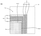
- FIG. 2 is an enlarged view of a region A in FIG.
- the high-frequency module 1 a includes a wiring board 2, a plurality of components 3 a mounted on the upper surface 2 a of the wiring board 2, and each of the components provided on the upper surface 2 a of the wiring board 2.
- a mother substrate of an electronic device including a sealing resin layer 4a for sealing the component 3a and first and second shield layers 5 and 6 (corresponding to the “shield layer” of the present invention), for example, using a high-frequency signal Etc.
- the wiring board 2 is formed of, for example, a low-temperature co-fired ceramic or glass epoxy resin, and a plurality of land electrodes for mounting each component 3a are provided on the upper surface (corresponding to “one main surface of the wiring board” of the present invention). 7 is formed.
- ground electrodes 8a and 8b for grounding, various wiring electrodes (not shown), and a plurality of via conductors (not shown) are formed inside.
- the ground electrodes 8 a and 8 b are both provided so as to be exposed from the side surface 2 b of the wiring board 2.
- Each land electrode 7, ground electrodes 8a and 8b, and wiring electrodes are each formed of a metal generally employed as a wiring electrode such as Cu or Al.
- Each via conductor is formed of a metal such as Ag or Cu.
- Each land electrode 7 may be subjected to Ni / Au plating.
- each component 3a examples include semiconductor elements formed of semiconductors such as Si and GaAs, and chip components such as chip inductors, chip capacitors, and chip resistors. Each component 3a corresponds to a “first component” of the present invention.
- the sealing resin layer 4a (corresponding to the “first sealing resin layer” of the present invention) is provided so as to cover the upper surface 2a of the wiring board 2 and each component 3a.
- the sealing resin layer 4a can be formed of a resin generally employed as a sealing resin such as an epoxy resin.
- the first shield layer 5 is laminated on the sealing resin layer 4a so as to cover the surface 4a1 and the peripheral side surface 4a2 of the sealing resin layer 4a opposite to the upper surface 2a of the wiring substrate 2 and the side surface 2b of the wiring substrate 2.
- the first shield layer 5 includes an adhesion film 5a laminated on the surface of the sealing resin layer 4a, and a conductive film 5b laminated on the adhesion film 5a (“first conductivity of the present invention”). And a protective film 5c laminated on the conductive film 5b, and is electrically connected to the ground electrodes 8a and 8b exposed on the side surface 2b of the wiring board 2.
- the adhesion film 5a is provided to increase the adhesion strength between the conductive film 5b and the sealing resin layer 4a.
- the adhesion film 5a is electrically connected to the ground electrodes 8a and 8b exposed on the side surface 2b on the side surface 2b of the wiring board 2.
- the film thickness on the opposite surface 4a1 of the sealing resin layer 4a of the adhesion film 5a is preferably 0.01 ⁇ m or more and 0.5 ⁇ m or less.
- the adhesion film 5a is formed of SUS.
- the conductive film 5b is a layer that bears the substantial shielding function of the first shield layer 5, and can be formed of any metal of Cu, Ag, and Al, for example.
- the film thickness on the opposite surface 4a1 of the sealing resin layer 4a of the conductive film 5b is preferably 3 ⁇ m or more and 10 ⁇ m or less.
- the conductive film 5b is made of Cu.
- the thickness of the conductive film 5b is 3 ⁇ m or more, the conductive film 5b can effectively prevent noise from above the high-frequency module 1a from affecting each component 3a.
- the thickness of the conductive film 5b is 10 ⁇ m or less, the high-frequency module 1a can be reduced in height.
- the protective film 5c is provided to prevent the conductive film 5b from being corroded or scratched.
- SUS, Ti, Cr, Ni, TiCr, TiAl, NiAl, CrAl, CrNiAl It can be formed of any of the metals.
- the thickness of the sealing resin layer 4a of the protective film 5c on the opposite surface 4a1 is preferably 0.03 ⁇ m or more and 1.5 ⁇ m or less.
- the protective film 5c is made of SUS.
- the second shield layer 6 is provided to reinforce the first shield layer 5, and the first shield layer 5 covers the portion covering the peripheral side surface 4 a 2 of the sealing resin layer 4 a.
- a single shield layer 5 is laminated.
- the second shield layer 6 includes an adhesion film 6a laminated on a portion covering the peripheral side surface 4a2 of the sealing resin layer 4a of the protective film 5c, like the first shield layer 5.
- the conductive film 6b (corresponding to the “second conductive film” of the present invention) laminated on the adhesion film 6a and the protective film 6c laminated on the conductive film 6b are formed.
- the second shield layer 6 is provided so as to cover the peripheral side surface of the first shield layer 5 (protective film 5c), and the upper surface of the first shield layer 5 (protective film 5c) is covered. Not. Therefore, the 1st shield layer 5 is exposed to the part located on the said opposite surface 4a1 of the sealing resin layer 4a among the shield layers (the 1st shield layer 5 and the 2nd shield layer 6).
- the adhesion film 6a of the second shield layer 6 has the same configuration as the adhesion film 5a of the first shield layer 5, and the conductive film 6b of the second shield layer 6 has the same configuration as the conductive film 5b of the first shield layer 5.
- the protective film 6 c of the second shield layer 6 can be formed with the same configuration as the protective film 5 c of the first shield layer 5.
- each component 3a is mounted on the upper surface 2a of the wiring board 2 formed of low temperature co-fired ceramic (LTCC), glass epoxy resin or the like.
- the wiring board 2 is formed with electrodes such as land electrodes 7, ground electrodes 8a and 8b, and via conductors by a known method.
- Each component 3a can be mounted using a general surface mounting technique such as solder mounting. Note that flux cleaning may be performed after each component 3a is mounted.
- each component 3a is sealed with an epoxy resin to form a sealing resin layer 4a.
- the wiring substrate 2, the component 3a mounted on the upper surface 2a of the wiring substrate 2, the upper surface 2a of the wiring substrate 2, and each A mold structure having a sealing resin layer 4a laminated on the upper surface 2a of the wiring board 2 so as to cover the component 3a is prepared.
- the sealing resin layer 4a can be formed by a coating method, a printing method, a transfer mold method, a compression mold method, or the like.
- the surface 4a1 opposite to the upper surface 2a of the wiring substrate 2 of the sealing resin layer 4a may be ground.
- dry cleaning such as plasma etching may be performed before the formation of the sealing resin layer 4a.
- a release film at the time of resin sealing of each component 3a such as a transfer mold system and a compression mold system, you may use what roughened the resin contact surface of the said release film.
- the surface roughness Ra of the sealing resin layer 4a is preferably 1 ⁇ m or more and 10 ⁇ m or less.
- the high-frequency module 1a with a multi-piece collective board in which a plurality of wiring boards 2 are integrally formed
- individual molds are used by a dicer, a laser, a router, or the like. Divide into structures.
- the aggregate substrate may be half cut.
- the ground electrodes 8 a and 8 b formed on the wiring board 2 are exposed on the side surface 2 b of the wiring board 2 at the time of cutting.
- the mold structures after separation are arranged and supported on a sputtering tray.
- a paste or tape may be applied to the lower surface of the wiring board 2 in order to prevent the sputtered film from entering the lower surface of the wiring board 2.
- the tray on which the mold structure is set is disposed at a predetermined position in the chamber of the sputtering apparatus, and the chamber is evacuated. At this time, the tray is arranged so that the opposite surface 4a1 of the sealing resin layer 4a faces each target of the sputtering apparatus.
- the ultimate vacuum is low.
- the time required for evacuation is increased accordingly, so that the set ultimate vacuum is 1 ⁇ 10 ⁇ 3 Pa or more and 1 ⁇ 10 6 from the viewpoint of productivity. ⁇ 1 Pa or less is preferable.
- the chamber may be composed of a sputtering chamber and a load lock chamber (so-called front chamber).
- a sputtering apparatus an in-line type, a batch type, a single wafer type, or the like can be used.
- an adhesion film 5a of the first shield layer 5 is formed by sputtering so as to cover the surface of the sealing resin layer 4a and the side surface 2b of the wiring board 2.
- any one of SUS, Ti, Cr, Ni, TiCr, TiAl, NiAl, CrAl, and CrNiAl can be used as a target material.
- a voltage is applied to the SUS target for a desired time and sputtering is performed.
- the film thickness at this time (the film thickness of the portion of the adhesive film 5a located on the opposite surface 4a1 of the sealing resin layer 4a) is 0.01 ⁇ m or more and 0.5 ⁇ m or less.
- Ar gas used as a plasma source is used as a gas to be introduced into the chamber.
- the input amount at this time is set to 30 to 300 sccm, for example.
- pre-sputtering sin-called sputtering with the shutter closed
- a sintered target etc. can be used for a target other than a metal target.
- Some metal targets are difficult to form depending on the composition of the alloy, but in the case of sintered targets, the metal composition ratio can be adjusted with any composition, making it easy to optimize adhesion and corrosion resistance. It can be carried out.
- the power system of the sputtering apparatus can use a DC system, a pulse system, an RF system, or the like.
- the pulse method or the RF method even when a reaction product (oxide or nitride) is formed on the target surface and the resistance value is increased, the discharge can be stably performed.
- a conductive film 5b is formed on the surface of the adhesion film 5a by sputtering.
- any one of Cu, Ag, and Al can be used as a target material.
- sputtering is performed by applying a voltage to the Cu target for a desired time.
- Ar gas used as a plasma source is used as a gas to be introduced into the chamber.
- the input amount at this time is set to 30 to 300 sccm, for example.
- pre-sputtering may be performed on the Cu target.
- the film thickness on the peripheral side surface 4a2 of the sealing resin layer 4a in the conductive film 5b is the opposite surface 4a1. It becomes about 30% of the upper film thickness.
- the film thickness of the conductive film 5b is 3 ⁇ m or more and 10 ⁇ m or less on the opposite surface 4a1 of the sealing resin layer 4a
- the film thickness on the peripheral side surface 4a2 of the sealing resin layer 4a of the conductive film 5b is on the opposite surface 4a1.
- the conductive film 5b generally needs to have a thickness that is twice or more the high frequency skin depth ⁇ . Therefore, when the conductive film 5b is Cu, the thickness of the conductive film 5b needs to be about 2.7 ⁇ m in the 2.4 GHz band and about 1.8 ⁇ m in the 5 GHz band.
- the film thickness on the peripheral side surface 4a2 is about 0.9 ⁇ m.
- the film thickness on the opposite surface 4a1 of the sealing resin layer 4a of the conductive film 5b is 3 ⁇ m, and a sufficient shielding function is obtained.
- the film thickness on the peripheral side surface 4a2 of the sealing resin layer 4a of the conductive film 5b is about 0.9 ⁇ m, which is insufficient by about 2 ⁇ m to ensure a sufficient shielding function. Therefore, in this embodiment, the second shield layer 6 is formed to compensate for the shortage.
- the first shield layer 5 is completed by forming a protective film 5c on the surface of the conductive film 5b by sputtering in the same manner as the adhesion film 5a.
- a protective film 5c on the surface of the conductive film 5b by sputtering in the same manner as the adhesion film 5a.
- any one of SUS, Ti, Cr, Ni, TiCr, TiAl, NiAl, CrAl, and CrNiAl can be used as a target material.
- the film thickness of the protective film 5c at this time (the film thickness of the portion of the protective film 5c located on the opposite surface 4a1 of the sealing resin layer 4a) is 0.03 ⁇ m or more and 1.5 ⁇ m or less.
- the portions of the adhesion film 5a and the protective film 5c that are located on the peripheral side surface 4a2 of the sealing resin layer 4a have the thicknesses of the adhesion film 5a and the protective film 5c, respectively. It is about 30% of the portion located on the opposite surface 4a1 of the sealing resin layer 4a. Therefore, the film thickness of the portion located on the peripheral side surface 4a2 of the sealing resin layer 4a in the adhesion film 5a is, for example, 0.003 ⁇ m or more and 0.15 ⁇ m or less, and the periphery of the sealing resin layer 4a in the protective film 5c.
- the film thickness of the portion located on the side surface 4a2 is, for example, 0.009 ⁇ m or more and 0.45 ⁇ m or less.
- the conductive film 5b is a film that performs a substantial shielding function, and the shielding characteristics of the first shield layer 5 improve as the film thickness increases. In view of these circumstances, it is preferable that the thickness of each adhesion film 5a, conductive film 5b, and protective film 5c of the first shield layer 5 is the largest in the conductive film 5b and the smallest in the adhesion film 5a.
- first shield layer 5 covering the opposite surface 4a1 of the sealing resin layer 4a is masked with a tape or paste, and then the second shield layer 5 in the same manner as the adhesion film 5a of the first shield layer 5.
- An adhesion film 6a for the shield layer 6 is formed.
- a metal mask may be used as the mask.
- the conductive film 6 b of the second shield layer 6 is formed in the same manner as the conductive film 5 b of the first shield layer 5.
- the film thickness of the conductive film 6b at this time is preferably equal to or greater than the film thickness of the conductive film 5b of the first shield layer 5 (film thickness on the peripheral side surface 4a2 side of the sealing resin layer 4a).
- the protective film 6 c of the second shield layer 6 is formed in the same manner as the protective film 5 c of the first shield layer 5. Then, the high frequency module 1a is completed by taking out the tray from the sputtering apparatus and removing the mask.
- the adhesion film 6a, the conductive film 6b, and the protective film 6c of the second shield layer 6 are preferably formed of the same metal as the adhesion film 5a, the conductive film 5b, and the protective film 5c of the first shield layer 5, respectively.
- the manufacturing cost of the high-frequency module 1a can be reduced.
- the first shield layer 5 and the second shield layer 6 have the same configuration, the difference in thermal expansion coefficient between the shield layers 5 and 6 can be reduced. Peeling can be reduced.
- the 1st shield layer 5 and the 2nd shield layer 6 can be formed using a vacuum evaporation apparatus other than a sputtering device, for example.
- the first shield layer 5 provides desired shield characteristics. Even if it is a case where the thickness for obtaining cannot be ensured, the shortage can be secured by the second shield layer 6. Further, since the second shield layer 6 is not laminated on the side 4a1 opposite to the upper surface 2a of the wiring substrate 2 of the sealing resin layer 4a, only the first shield layer 5 is on the opposite surface 4a1 of the sealing resin layer 4a. Covered with. According to this configuration, it is possible to reduce the height of the high-frequency module 1a while ensuring desired shield characteristics.
- FIG. 3 is a partial cross-sectional view of the high-frequency module and corresponds to FIG.
- the high-frequency module 1b according to this embodiment differs from the high-frequency module 1a according to the first embodiment described with reference to FIGS. 1 and 2 in that the configuration of the second shield layer 60 is different as shown in FIG. That is. Since other configurations are the same as those of the high-frequency module 1a of the first embodiment, description thereof is omitted by attaching the same reference numerals.
- the second shield layer 60 is a magnetic film 60a (corresponding to the “third conductive film” of the present invention) laminated on a portion covering the peripheral side surface 4a2 of the sealing resin layer 4a of the first shield layer 5.
- the magnetic film 60 a is formed of a metal magnetic material having a relative permeability higher than that of the conductive film 5 b of the first shield layer 5.
- the relative permeability ⁇ s of metal Cu forming the conductive film 5 b of the first shield layer 5 is 0.999991
- the magnetic film 60a of the second shield layer 60 includes Ni having a relative permeability ⁇ s of 100 to 600, Permalloy having a relative permeability ⁇ s of 8000, Fe having a relative permeability ⁇ s of 5000, and the like. It is made of any metal.
- the magnetic film 60a of the second shield layer 60 is a metal having a relative permeability higher than that of Cu (for example, a relative permeability ⁇ s ⁇ What is necessary is just to be formed by 1).
- the protective film 60b can be formed with the same configuration as the protective film 5c of the first shield layer 5 such as, for example, formed of SUS.
- the conductive film 5b of the first shield layer 5 is formed of a metal magnetic material such as Ni, permalloy, and Fe, and the magnetic film 60a portion of the second shield layer 60 has a high conductivity such as Cu, Ag, and Al.
- the structure formed with the metal which it has may be sufficient. That is, the configuration of the conductive film 5b of the first shield layer 5 and the magnetic film 60a of the second shield layer 60 may be reversed.
- any one of the adhesion films 6a, the conductive films 6b, and the protective films 6c of the second shield layer 6 may be formed of a metal magnetic material such as Ni, permalloy, or Fe.
- the peripheral side surface 4a2 of the sealing resin layer 4a is covered with both the conductive film 5b having a high conductivity such as Cu and the magnetic film 60a having a high relative permeability.
- the shielding property against the magnetic field can be improved.
- the first shield layer 5 and the second shield layer can be obtained as compared with the configuration of the first embodiment in order to obtain a desired shield characteristic on the peripheral side surface 4a2 side of the sealing resin layer 4a.
- the total film thickness of 60 can be reduced. Therefore, the high-frequency module 1b can be reduced in height while the thickness of the first shield layer 5 and the second shield layer 60 on the peripheral side surface 4a2 side of the sealing resin layer 4a can be reduced. be able to.
- FIG. 4 is a cross-sectional view of the high frequency module.
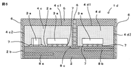
- the high-frequency module 1c according to this embodiment is different from the high-frequency module 1a according to the first embodiment described with reference to FIGS. 1 and 2 as shown in FIG. And the component 3b is covered with the sealing resin layer 4b, and the first shield layer 5 and the second shield layer 6 are The sealing resin layer 4b on the lower surface 2c side of the wiring board 2 is also covered. Since other configurations are the same as those of the high-frequency module 1a of the first embodiment, description thereof is omitted by attaching the same reference numerals.
- the component 3b (corresponding to the “second component” of the present invention) is a semiconductor element formed of a semiconductor such as Si or GaAs, a chip inductor, or a chip capacitor, like each component 3a on the upper surface 2a side of the wiring board 2. And chip components such as chip resistors.
- the encapsulating resin layer 4b (corresponding to the “second encapsulating resin layer” of the present invention and may be referred to as the second encapsulating resin layer 4b hereinafter) covers the lower surface 2c of the wiring board 2 and the component 3b. It is provided as follows.
- the sealing resin layer 4b is different from the sealing resin layer 4a (hereinafter sometimes referred to as the first sealing resin layer 4a) that covers the entire surface of the upper surface 2a of the wiring substrate 2, and the lower surface of the wiring substrate 2. Part of 2c is covered, and in this embodiment, the part not covered with the second sealing resin layer 4b is used as a space for connection to the outside of the high-frequency module 1c.
- the second sealing resin layer 4b may cover the entire lower surface 2c of the wiring board 2, or the first sealing resin layer 4a may also be a part of the wiring board 2 leaving a part of the upper surface 2a. You may make it coat
- the 2nd sealing resin layer 4b can be formed with resin generally employ
- the first shield layer 5 covers a part of the peripheral side surface 4b2 of the second sealing resin layer 4b in addition to the opposite surface 4a1 and the peripheral side surface 4a2 of the first sealing resin layer 4a.
- the second shield layer 6 includes a second sealing resin layer 4b in addition to a portion covering the peripheral side surface 4a2 of the first sealing resin layer 4a of the first shield layer 5 and a portion covering the side surface 2b of the wiring board 2.
- the surface 4b1 opposite to the lower surface 2c of the wiring board 2 and the portion of the peripheral side surface 4b2 of the second sealing resin layer 4b that is not covered with the first shield layer 5 are covered.
- the other configurations of the first shield layer 5 and the second shield layer 6 are the same as those in the first embodiment.
- the components 3a and 3b are mounted on the upper and lower surfaces 2a and 2c of the wiring substrate 2, and the components 3a and 3b on both surfaces 2a and 2c of the wiring substrate 2 are molded with the first and second sealing resin layers 4a and 4b.
- a mold structure is formed.
- the first sealing resin layer 4a molds the entire upper surface 2a of the wiring board 2
- the second sealing resin layer 4b is a part of the area where the component 3b of the lower surface 2c of the wiring board 2 is not mounted. Partially mold leaving part.
- Each of the first and second sealing resin layers 4a and 4b can be formed by a coating method, a printing method, a transfer molding method, a compression molding method, or the like.
- the first sealing resin layer 4a side that covers the entire upper surface 2a of the wiring substrate 2 is formed by a coating method or a compression molding method, and a second sealing resin that partially covers the lower surface 2c of the wiring substrate 2 is formed.
- the layer 4b side can also be formed by a transfer mold method.
- the formation method of the first shield layer 5 is the same as that of the high-frequency module 1a of the first embodiment, but the tray is disposed so that the opposite surface 4a1 of the first sealing resin layer 4a and each target of the sputtering apparatus face each other. Then, a part of the peripheral side surface 4b2 of the second sealing resin layer 4b is also covered with each adhesion film 5a, the conductive film 5b, and the protective film 5c of the first shield layer 5.
- the tray is taken out from the sputtering apparatus, the mold structure is turned over and set on the tray. A portion of the lower surface 2c of the wiring board 2 that does not require the formation of the second shield layer 6 is masked in advance using tape or paste. Then, a tray is again arranged in the sputtering apparatus, and the adhesion film 6a, the conductive film 6b, and the protective film 6c of the second shield layer 6 are formed in the same manner as the first shield layer 5. At this time, the tray is disposed so that the opposite surface 4b1 of the second sealing resin layer 4b faces each target.
- covers the surrounding side surface 4a2 of the 1st sealing resin layer 4a of the 1st shield layer 5
- covers the side surface 2b of the wiring board 2
- the second shield layer 6 covers each of the surface 4b1 opposite to the lower surface 2c and the portions of the peripheral side surface 4b2 of the second sealing resin layer 4b that are not covered by the first shield layer 5.
- the mold structure is turned over and film formation is performed twice, so that the side surfaces of the mold structure (the peripheral side surfaces 4a2 and 4b2 of the first and second sealing resin layers 4a and 4b and the wiring substrate 2)
- the side surface 2 b) can be covered with both the first shield layer 5 and the second shield layer 6.
- both the opposite surfaces 4a1 and 4b1 side of the first and second sealing resin layers 4a formed to be thicker than the peripheral side surfaces 4a2 and 4b2 are both the first shield layer 5 and the second shield layer 5a.
- the first and second sealing resin layers 4a and 4b, which are coated with only one of the shield layers 6, have the first shield layer 5 and the second shield layer on the side surfaces 4a2 and 4b2 of the thin sealing resin layers 4a and 4b. 6 are both coated. Therefore, it is possible to reduce the height of the high-frequency module 1c while ensuring the shielding characteristics on the side surfaces 4a2 and 4b2 of the first and second sealing resin layers 4a and 4b.
- FIG. 5 is a cross-sectional view of the high-frequency module.
- the high-frequency module 1d according to this embodiment differs from the high-frequency module 1a according to the first embodiment described with reference to FIGS. 1 and 2 in that each component 3a has two seals as shown in FIG.
- the resin layers 4c and 4d are separately molded, the sealing resin layers 4c and 4d are individually covered with the first shield layer 5 and the second shield layer 6, and the wiring board 2 Is provided with another ground electrode 8c. Since other configurations are the same as those of the high-frequency module 1a of the first embodiment, description thereof is omitted by attaching the same reference numerals.
- the first shield layer 5 is opposite to the upper surface 2a of the sealing substrate 4c1 and the peripheral surface 4c2 opposite to the upper surface 2a of the wiring substrate 2 of one sealing resin layer 4c, and the upper surface 2a of the wiring substrate of the other sealing resin layer 4d.
- the surface 4d1, the peripheral side surface 4d2, and the side surface 2b of the wiring board 2 are covered.
- the second shield layer 6 includes a portion covering the peripheral side surface 4c2 of one sealing resin layer 4c of the first shield layer 5, a portion covering the peripheral side surface 4d2 of the other sealing resin layer 4d, and a side surface of the wiring board 2. It is laminated
- the first shield layer 5 and the second shield layer 6 are interposed between the sealing resin layers 4c and 4d.
- a portion of the first shield layer 5 located between both the sealing resin layers 4 c and 4 d is connected to a ground electrode 8 c formed on the wiring board 2.
- each of the sealing resin layers 4c and 4d corresponds to the “first sealing resin layer” of the present invention.
- each component 3a is collectively sealed with resin, a groove is formed between the predetermined components 3a using a laser or a dicer. Then, it can form by forming the 1st shield layer 5 and the 2nd shield layer 6 by the same method as the high frequency module 1a of 1st Embodiment.
- the first shield layer 5 and the second shield layer 6 are interposed between the sealing resin layers 4c and 4d, so that one of the seals is sealed. It is possible to prevent mutual interference of noise between the component 3a sealed in the stop resin layer 4c and the component 3a sealed in the other sealing resin layer 4d.
- FIG. 6 is a partial cross-sectional view of the high-frequency module, and corresponds to FIG.
- the high-frequency module 1e according to this embodiment differs from the high-frequency module 1a according to the first embodiment described with reference to FIGS. 1 and 2 in that the configuration of the third shield layer 50 is different as shown in FIG. That is. Since other configurations are the same as those of the high-frequency module 1a of the first embodiment, description thereof is omitted by attaching the same reference numerals.
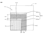
- the third shield layer 50 has substantially the same three-layer structure as the first shield layer 5 of the first embodiment. Specifically, as shown in FIG. 6, the third shield layer 50 is formed of a sealing resin layer so as to cover the opposite surface 4a1 and peripheral side surface 4a2 of the sealing resin layer 4a and the side surface 2b of the wiring board 2. 4a, an adhesion film 50a laminated on the adhesion film 50a, a conductive film 50b laminated on the adhesion film 50a, and a protective film 50c laminated on the conductive film 50b.
- Each adhesion film 50a, conductive film 50b, and protective film 50c of the third shield layer 50 has the same configuration as each adhesion film 5a, conductive film 5b, and protective film 5c of the first shield layer 5.
- the ratio of the thickness a2 on the peripheral side surface 4a2 side to the thickness a1 on the opposite surface 4a1 side of the sealing resin layer 4a of the adhesion film 50a is the opposite surface of the sealing resin layer 4a of the conductive film 50b. It is formed to be smaller than the ratio of the thickness b2 on the peripheral side surface 4a2 side to the thickness b1 on the 4a1 side ((a2 / a1) ⁇ (b2 / b1)).
- the third shield layer 50 can be formed as follows, for example. Until the adhesion film 50a is formed, it is formed in the same manner as the high-frequency module 1a in the first embodiment, and the conductive film 50b is first in the same manner as the conductive film 5b in the first shield layer 5 in the first embodiment. Form a film. Thereafter, the tray is taken out from the sputtering apparatus, a mask is applied to the portion of the conductive film 5b that covers the opposite surface 4a1 of the sealing resin layer 4a, and the second conductive film 50b is formed again in the same manner. If it does so, a film thickness can be increased only in the part which coat
- the present invention is not limited to the above-described embodiments, and various modifications other than those described above can be made without departing from the spirit of the invention.
- membrane 6a of the 2nd shield layer 6 may be sufficient.
- the present invention can be applied to various high-frequency modules including a sealing resin layer that covers a component mounted on a wiring board and a shield layer laminated on the sealing resin layer.
Landscapes
- Engineering & Computer Science (AREA)
- Microelectronics & Electronic Packaging (AREA)
- Chemical & Material Sciences (AREA)
- Ceramic Engineering (AREA)
- Physics & Mathematics (AREA)
- Electromagnetism (AREA)
- Materials Engineering (AREA)
- Chemical Kinetics & Catalysis (AREA)
- Inorganic Chemistry (AREA)
- Mechanical Engineering (AREA)
- Metallurgy (AREA)
- Organic Chemistry (AREA)
- Shielding Devices Or Components To Electric Or Magnetic Fields (AREA)
- Structures Or Materials For Encapsulating Or Coating Semiconductor Devices Or Solid State Devices (AREA)
- Health & Medical Sciences (AREA)
- Toxicology (AREA)
- Condensed Matter Physics & Semiconductors (AREA)
- General Physics & Mathematics (AREA)
Abstract
シールド特性を確保しつつ、低背化を図ることができる高周波モジュールを提供する。 高周波モジュール1aは、配線基板2と、配線基板2の上面2aに実装された部品3aと、配線基板2の上面2aに積層されて部品3aを封止する封止樹脂層4aと、第1封止樹脂層4aの配線基板2の上面2aとの反対面4a1および周側面4a2を被覆するように封止樹脂層4aに積層された第1シールド層5と、第1シールド層5の封止樹脂層4aの周側面4a2を被覆する部分に積層された第2シールド層5とを備える。この場合、第1シールド層5で所望のシールド特性を得るための厚みを確保できない場合であっても、その不足分を第2シールド層6で担保することができるため、所望のシールド特性を確保しつつ、高周波モジュール1aの低背化を図ることができる。
Description
本発明は、配線基板に実装された部品を被覆する封止樹脂層と、封止樹脂層に積層されたシールド層とを備えるモジュールに関する。
携帯端末装置などに搭載される高周波モジュールには、電磁波を遮蔽するためのシールド層が設けられる場合がある。この種の高周波モジュールの中には、配線基板上に実装された部品がモールド樹脂で被覆され、該モールド樹脂の表面を被覆するようにシールド層が設けられるものがある。シールド層は、電磁波のシールドを目的として、CuやAl、Agなどの導電膜を有するのが一般的であるが、これらの金属膜は、いずれもモールド樹脂との密着強度が弱く、耐腐食性も十分ではないという課題がある。
そこで、従来では、樹脂との密着性が高く、耐腐食性に優れたシールド層が提案されている。例えば、図7に示すように、特許文献1に記載の高周波モジュール100は、樹脂基板101と、該樹脂基板101の上面に積層されたシールド層102とを備え、シールド層102が、樹脂基板101上に成膜された密着膜102aと、該密着膜102a上に成膜された導電膜102bと、該導電膜102b上に成膜された保護膜102cの3層構造で形成される。ここで、導電膜102bは、Cu、Ag、Alのうちのいずれかで形成される。また、密着膜102aは、樹脂基板101との密着強度が導電膜102bよりも高いSUSで形成される。また、導電膜102b上に成膜される保護膜102cは、導電膜102bよりも耐腐食性の高いSUSで形成されている。このように、シールド層102を3層構造で形成することで、密着強度と耐腐食性等の向上が図られている。
上述のシールド層102は、スパッタリング法や、蒸着法などの薄膜形成技術を用いて形成される。この場合、樹脂基板101の主面を、ターゲットや蒸着源に対向するように配置して成膜するのが一般的である。したがって、配線基板上に実装された部品がモールド樹脂で被覆され、該モールド樹脂の表面を被覆するようにシールド層を形成する構成では、モールド樹脂の天面を、ターゲットや蒸着源に対向するように配置して成膜する。
このような成膜方法によると、シールド層の厚みは、モールド樹脂の天面を被覆する部分が、モールド樹脂の周側面を被覆する部分よりも厚くなる。そのため、所望のシールド特性を得るべくシールド層の周側面側の厚みを確保しようとすると、天面側の厚みが必要以上に厚くなって、高周波モジュールの低背化の妨げになっていた。
本発明は、上記した課題に鑑みてなされたものであり、シールド特性を確保しつつ、低背化を図ることができる高周波モジュールを提供することを目的とする。
上記した目的を達成するために、本発明の高周波モジュールは、配線基板と、前記配線基板の一方主面に実装された第1部品と、前記配線基板の前記一方主面に積層され、前記第1部品を封止する第1封止樹脂層と、前記第1封止樹脂層に積層されたシールド層とを備え、前記シールド層は、前記第1封止樹脂層のうち前記配線基板の前記一方主面との反対面および周側面を被覆するように前記第1封止樹脂層に積層された第1シールド層と、前記第1シールド層のうち前記第1封止樹脂層の前記周側面を被覆する部分に積層された第2シールド層とを有することを特徴としている。
この場合、第1封止樹脂層の周側面は、第1シールド層と第2シールド層とで被覆されるため、第1シールド層で所望のシールド特性を得るための厚みを確保できない場合であっても、その不足分を第2シールド層で担保することができる。また、第2シールド層は、第1封止樹脂層の配線基板の一方主面との反対面側には積層されないため、第1封止樹脂層の前記反対面は第1シールド層で被覆される。この構成によると、所望のシールド特性を確保しつつ、高周波モジュールの低背化を図ることができる。
また、前記第1シールド層は、金属から成る第1導電膜を有し、前記第2シールド層は、前記第1導電膜と同じ金属から成る第2導電膜を有していてもよい。この場合、第1シールド層と第2シールド層とで熱膨張率の差を小さくすることができるため、ヒートショック時の両シールド層間の剥がれを低減することができる。また、両シールド層をスパッタ法や蒸着法などで形成する場合には、ターゲットや蒸着源の共通化を図ることができるため、両シールド層の形成コストの低減を図ることができる。
また、前記第1シールド層は、金属から成る第1導電膜を有し、前記第2シールド層は、前記第1導電膜とは異なる金属から成る第3導電膜を有し、前記第1導電膜の前記金属および前記第3導電膜の前記異なる金属のうちの一方は、比透磁率が1以上であってもよい。この場合、例えば、第1導電膜を形成する金属に導電率の高い銅やアルミなどを使用し、第2導電膜を形成する金属に高透磁率のNiやCoなどを使用することができる。この構成によると、第2シールド層の電界のみならず磁界に対するシールド特性の向上を図ることができる。
また、前記配線基板の他方主面に実装された第2部品と、前記配線基板の前記他方主面に積層されて前記第2部品を封止する第2封止樹脂層とをさらに備え、前記第1シールド層は、前記第2封止樹脂層の周側面をさらに被覆し、前記第2シールド層は、前記第1シールド層のうち前記第1封止樹脂層の前記周側面を被覆する部分に加えて、前記第1シールド層のうち前記第2封止樹脂層の前記周側面を被覆する部分、および、前記第2封止樹脂層のうち前記配線基板の前記他方主面との反対面を被覆するように設けられていてもよい。
この場合、第1封止樹脂層の周側面および第2封止樹脂層の周側面の両方が、第1シールド層と第2シールド層とにより被覆される。第1、第2シールド層の一方で所望のシールド特性を得るための厚みを確保できない場合であっても、その不足分を他方のシールド層で担保することができる。また、第1封止樹脂層の配線基板の一方主面との反対面および第2封止樹脂層の配線基板の他方主面との反対面は、いずれも第1シールド層および第2シールド層の一方のみで被覆される。したがって、第1および第2封止樹脂層の周側面側のシールド特性を確保しつつ、高周波モジュールの低背化を図ることができる。
また、前記シールド層のうち、前記第1封止樹脂層の前記反対面を覆う部分の表面には、前記第1シールド層が露出していてもよい。このようにすると、高周波モジュールの低背化を図ることができる。
また、配線基板と、前記配線基板の一方主面に実装された第1部品と、前記配線基板の前記一方主面に積層されて前記第1部品を封止する第1封止樹脂層と、前記第1封止樹脂層のうち前記配線基板の前記一方主面との反対面および周側面を被覆するように前記第1封止樹脂層に積層された第3シールド層とを備え、前記第3シールド層は、前記第1封止樹脂層に積層された密着膜と、該密着膜に積層された導電膜とを有し、前記密着膜の前記反対面側の厚みに対する前記周側面側の厚みの割合は、前記導電膜の前記反対面側の厚みに対する前記周側面側の厚みの割合よりも小さくてもよい。
導電膜の導電率は密着膜よりも高い場合が多く、この場合は、導電膜の厚みが厚いほど、第3シールド層のシールド特性が高くなる。この構成によると、例えば、導電膜と密着膜の第1封止樹脂層の前記反対面側の厚みを、同じ厚みとすると、第1封止樹脂層の周側面側の厚みは、密着膜よりも導電膜の方が厚くなる。そのため、第3シールド層において、第1封止樹脂層の周側面側のシールド特性を容易に向上することができる。
本発明によれば、第1封止樹脂層の周側面は、第1シールド層と第2シールド層とで被覆されるため、第1シールド層で所望のシールド特性を得るための厚みを確保できない場合であっても、その不足分を第2シールド層で担保することができる。また、第2シールド層は、第1封止樹脂層の配線基板の一方主面との反対面側には積層されないため、第1封止樹脂層の反対面は第1シールド層で被覆される。この構成によると、所望のシールド特性を確保しつつ、高周波モジュールの低背化を図ることができる。
<第1実施形態>
本発明の第1実施形態にかかる高周波モジュール1aについて、図1および図2を参照して説明する。なお、図1は高周波モジュールの断面図、図2は図1のA領域の拡大図である。
本発明の第1実施形態にかかる高周波モジュール1aについて、図1および図2を参照して説明する。なお、図1は高周波モジュールの断面図、図2は図1のA領域の拡大図である。
この実施形態にかかる高周波モジュール1aは、図1に示すように、配線基板2と、該配線基板2の上面2aに実装された複数の部品3aと、配線基板2の上面2aに設けられた各部品3aを封止する封止樹脂層4aと、第1、第2シールド層5,6(本発明の「シールド層」に相当)とを備え、例えば、高周波信号が用いられる電子機器のマザー基板等に搭載される。
配線基板2は、例えば、低温同時焼成セラミックやガラスエポキシ樹脂などで形成され、上面(本発明の「配線基板の一方主面」に相当)には、各部品3aの実装用の複数のランド電極7が形成される。また、内部には、接地用のグランド電極8a,8bや各種配線電極(図示省略)、並びに複数のビア導体(図示省略)が形成されている。ここで、グランド電極8a,8bは、いずれも配線基板2の側面2bから露出するように設けられている。
各ランド電極7、グランド電極8a,8bおよび配線電極は、それぞれCuやAl等の配線電極として一般的に採用される金属で形成されている。また、各ビア導体は、AgやCu等の金属で形成されている。なお、各ランド電極7には、Ni/Auめっきがそれぞれ施されていてもよい。
各部品3aとしては、SiやGaAs等の半導体で形成された半導体素子や、チップインダクタ、チップコンデンサ、チップ抵抗等のチップ部品などが挙げられる。各部品3aそれぞれが、本発明の「第1部品」に相当する。
封止樹脂層4a(本発明の「第1封止樹脂層」に相当)は、配線基板2の上面2aと各部品3aとを被覆するように設けられている。この封止樹脂層4aは、エポキシ樹脂等の封止樹脂として一般的に採用される樹脂で形成することができる。
第1シールド層5は、封止樹脂層4aの配線基板2の上面2aとの反対面4a1および周側面4a2、並びに配線基板2の側面2bを被覆するように封止樹脂層4aに積層される。また、図2に示すように、第1シールド層5は、封止樹脂層4aの表面に積層された密着膜5aと、密着膜5aに積層された導電膜5b(本発明の「第1導電膜」に相当)と、導電膜5bに積層された保護膜5cとを有する多層構造で形成され、配線基板2の側面2bに露出したグランド電極8a,8bと電気的に接続されている。
密着膜5aは、導電膜5bと封止樹脂層4aとの密着強度を高めるために設けられたものであり、例えば、SUS、Ti、Cr、Ni、TiCr、TiAl、NiAl、CrAl、CrNiAlのうちのいずれかの金属で形成することができる。また、密着膜5aは、配線基板2の側面2bで、当該側面2bに露出したグランド電極8a,8bに電気的に接続される。密着膜5aの封止樹脂層4aの前記反対面4a1上の膜厚は、0.01μm以上0.5μm以下であるのが好ましい。なお、この実施形態では、密着膜5aが、SUSで形成されている。
導電膜5bは、第1シールド層5の実質的なシールド機能を担う層であり、例えば、Cu、Ag、Alのうちのいずれかの金属で形成することができる。導電膜5bの封止樹脂層4aの前記反対面4a1上の膜厚は、3μm以上10μm以下であるのが好ましい。なお、この実施形態では、導電膜5bが、Cuで形成されている。導電膜5bの厚さが3μm以上であることにより、高周波モジュール1aの上方からのノイズが各部品3aに影響を与えるのを、導電膜5bによって効果的に防止できる。また、導電膜5bの厚さが10μm以下であることにより、高周波モジュール1aの低背化を図ることができる。
保護膜5cは、導電膜5bが腐食したり、傷が付くのを防止するために設けられたものであり、例えば、SUS、Ti、Cr、Ni、TiCr、TiAl、NiAl、CrAl、CrNiAlのうちのいずれかの金属で形成することができる。保護膜5cの封止樹脂層4aの前記反対面4a1上の膜厚は、0.03μm以上1.5μm以下であるのが好ましい。なお、この実施形態では、保護膜5cがSUSで形成されている。
第2シールド層6は、第1シールド層5を補強するために設けられたものであり、第1シールド層5の封止樹脂層4aの周側面4a2を被覆する部分を被覆するように、第1シールド層5に積層される。また、図2に示すように、第2シールド層6は、第1シールド層5と同様に、保護膜5cの封止樹脂層4aの周側面4a2を被覆する部分に積層された密着膜6aと、密着膜6aに積層された導電膜6b(本発明の「第2導電膜」に相当)と、導電膜6bに積層された保護膜6cとを有する多層構造で形成されている。
図2に示すように、第2シールド層6は、第1シールド層5(保護膜5c)の周側面を覆うように設けられており、第1シールド層5(保護膜5c)の上面は覆っていない。そのため、シールド層(第1シールド層5および第2シールド層6)のうち封止樹脂層4aの前記反対面4a1上に位置する部分には、第1シールド層5が露出している。
第2シールド層6の密着膜6aは、第1シールド層5の密着膜5aと同じ構成で、第2シールド層6の導電膜6bは、第1シールド層5の導電膜5bと同じ構成で、第2シールド層6の保護膜6cは、第1シールド層5の保護膜5cと同じ構成でそれぞれ形成することができる。
(高周波モジュールの製造法)
次に、高周波モジュール1aの製造方法について説明する。なお、この実施形態では、スパッタ装置を用いて第1シールド層5および第2シールド層6を形成する高周波モジュール1aの製造方法を例として説明する。
次に、高周波モジュール1aの製造方法について説明する。なお、この実施形態では、スパッタ装置を用いて第1シールド層5および第2シールド層6を形成する高周波モジュール1aの製造方法を例として説明する。
まず、低温同時焼成セラミック(LTCC)やガラスエポキシ樹脂等で形成された配線基板2の上面2aに各部品3aを実装する。なお、配線基板2には、ランド電極7、グランド電極8a,8bおよびビア導体などの電極が周知の方法で形成されている。また、各部品3aは、半田実装等、一般的な表面実装技術を用いて実装することができる。なお、各部品3aを実装後に、フラックス洗浄を行ってもよい。
次に、各部品3aをエポキシ樹脂で封止して封止樹脂層4aを形成し、配線基板2と、配線基板2の上面2aに実装された部品3aと、配線基板2の上面2aおよび各部品3aを被覆するように当該配線基板2の上面2aに積層された封止樹脂層4aとを有するモールド構造体を準備する。封止樹脂層4aは、塗布方式、印刷方式、トランスファモールド方式、コンプレッションモールド方式等で形成することができる。
なお、高周波モジュール1aの高さを均一にするために封止樹脂層4aの形成後に、封止樹脂層4aの配線基板2の上面2aとの反対面4a1を研削加工してもよい。また、封止樹脂層4aと配線基板2との密着性を高めるために、封止樹脂層4aの形成前にプラズマエッチングなどのドライ洗浄を行ってもよい。また、トランスファモールド方式やコンプレッションモールド方式など、各部品3aの樹脂封止時に離形フィルムを使用する場合は、当該離形フィルムの樹脂接触面が粗化されたものを使用してもよい。この場合、封止樹脂層4aの表面に凹凸が形成されるため、封止樹脂層4aの表面に手脂などが付着しにくく、小さな傷や汚れ等の外観の不具合も目立ちにくくなる。なお、この場合の封止樹脂層4aの表面粗さRaは、1μm以上10μm以下であることが好ましい。
次に、複数の配線基板2が一体的に形成された多数個取りの集合基板で高周波モジュール1aを製造する場合は、封止樹脂層4aの形成後に、ダイサーやレーザ、ルーターなどにより個々のモールド構造体に個片化する。この場合、集合基板をハーフカットするようにしてもよい。ハーフカットの場合、集合基板の状態で、第1シールド層5および第2シールド層6の成膜を行うことができるので、作業性がよい。なお、カット時に、配線基板2に形成されたグランド電極8a,8bが、配線基板2の側面2bにそれぞれ露出する。
次に、個片化後のモールド構造体をスパッタ用のトレイに並べて支持する。この場合、配線基板2の下面にスパッタによる膜が周り込むのを防止するために、配線基板2の下面にペーストやテープを貼ってもよい。
次に、モールド構造体がセットされたトレイをスパッタ装置のチャンバの所定位置に配置して、チャンバ内の真空引きを行う。このとき、封止樹脂層4aの前記反対面4a1とスパッタ装置の各ターゲットとが対向するようにトレイを配置する。なお、膜質を鑑みると到達真空度は低い方が好ましいが、それに伴って真空引きの所要時間が長くなるため、生産性の面から設定到達真空度は、1×10⁻³Pa以上1×10⁻¹Pa以下であることが好ましい。また、真空引きの所要時間を減らすため、チャンバ内をスパッタ室とロードロック室(いわゆる、前室)とで構成してもよい。また、スパッタ装置としては、インライン型、バッチ型、枚葉型などを使用することができる。
次に、必要に応じてスパッタ前にモールド構造体の表面のドライエッチングを行う。この場合、Arイオンガンに所要時間、電圧を印加してArイオンで封止樹脂層4aの表面(反対面4a1および周側面4a2)および配線基板2の側面2bをドライ洗浄する。このようにすると、第1シールド層5と封止樹脂層4aとの密着力の低下の原因となる不要物を除去できるのに加え、モールド構造体の表面が粗化されることによりアンカー効果が生じ、封止樹脂層4aと第1シールド層5(密着膜5a)の密着性が向上する。
次に、封止樹脂層4aの表面および配線基板2の側面2bを被覆するように、第1シールド層5の密着膜5aをスパッタにより成膜する。この場合、ターゲットの材料として、SUS、Ti、Cr、Ni、TiCr、TiAl、NiAl、CrAl、CrNiAlのうちのいずれかの金属を使用することができる。例えば、密着膜5aをSUSで形成する場合は、SUSターゲットに所望時間、電圧を印加してスパッタする。このときの膜厚(密着膜5aのうち、封止樹脂層4aの反対面4a1上に位置する部分の膜厚)は、0.01μm以上0.5μm以下とする。チャンバ内に投入するガスはプラズマ源となるArガスを使用する。また、このときの投入量は、例えば30~300sccmとする。
なお、ターゲットの表面の酸化物を除去するために、プリスパッタ(いわゆる、シャッタを閉じた状態でのスパッタ)を行ってもよい。また、ターゲットは、メタルターゲットのほか、焼結ターゲット等を使用することができる。メタルターゲットは、合金の組成によって形成が難しいものがあるが、焼結ターゲットの場合は、任意の組成で金属組成比を調整することができるため、密着性や耐腐食性の最適化を容易に行うことができる。
また、スパッタ装置の電力方式は、DC方式、パルス方式、RF方式等を使用することができる。パルス方式やRF方式の場合、ターゲット表面に反応物(酸化物、窒化物)が成膜されて抵抗値が高くなった場合でも、安定して放電することができる。
次に、密着膜5aと同じ要領で、当該密着膜5aの表面に、導電膜5bをスパッタで成膜する。この場合、ターゲットの材料として、Cu、Ag、Alのうちのいずれかの金属を使用することができる。例えば、導電膜5bをCuで形成する場合は、Cuターゲットに所望時間、電圧を印加してスパッタする。チャンバ内に投入するガスはプラズマ源となるArガスを使用する。また、このときの投入量は、例えば30~300sccmとする。また、密着膜5aと同様に、Cuターゲットにプリスパッタを行ってもよい。
ところで、封止樹脂層4aの前記反対面4a1を各ターゲットに対向するようにトレイを配置した場合、導電膜5bのうち封止樹脂層4aの周側面4a2上の膜厚は、前記反対面4a1上の膜厚の約30%になる。導電膜5bの膜厚が、封止樹脂層4aの前記反対面4a1上で3μm以上10μm以下の場合、導電膜5bの封止樹脂層4aの周側面4a2上の膜厚は、反対面4a1上の約30%の0.9μm以上3μm以下程度になる。十分なシールド効果を得るには、導電膜5bは一般的に高周波の表皮深さδの2倍以上の厚みが必要である。そのため、導電膜5bがCuの場合、導電膜5bの厚みは、2.4GHz帯で約2.7μm、5GHz帯で約1.8μmが必要となる。
例えば、導電膜5bの封止樹脂層4aの反対面4a1上の膜厚を3μmで形成すると、周側面4a2上の膜厚は約0.9μmとなる。この構成で2.4GHz帯の信号を遮蔽する場合、導電膜5bの封止樹脂層4aの反対面4a1上の膜厚は3μmで、十分なシールド機能が得られる。これに対して、導電膜5bの封止樹脂層4aの周側面4a2上の膜厚は約0.9μmで、十分なシールド機能を確保するのに約2μm不足する。そこで、この実施形態では、第2シールド層6の形成により、当該不足分を補うように構成されている。
次に、密着膜5aと同じ要領で、導電膜5bの表面に、保護膜5cをスパッタで成膜することにより第1シールド層5が完成する。この場合、ターゲットの材料として、SUS、Ti、Cr、Ni、TiCr、TiAl、NiAl、CrAl、CrNiAlのうちのいずれかの金属を使用することができる。また、このときの保護膜5cの膜厚(保護膜5cのうち、封止樹脂層4aの反対面4a1上に位置する部分の膜厚)は、0.03μm以上1.5μm以下とする。
なお、導電膜5bの場合と同様に、密着膜5a、保護膜5cのうち封止樹脂層4aの周側面4a2上に位置する部分の膜厚は、それぞれ、密着膜5a、保護膜5cのうち封止樹脂層4aの反対面4a1上に位置する部分の約30%になる。したがって、密着膜5aのうち封止樹脂層4aの周側面4a2上に位置する部分の膜厚は、例えば、0.003μm以上0.15μm以下となり、保護膜5cのうち封止樹脂層4aの周側面4a2上に位置する部分の膜厚は、例えば、0.009μm以上0.45μm以下になる。
なお、密着膜5aに使用される金属であるSUS、Ti、Cr、Ni、TiCr、TiAl、NiAl、CrAl、CrNiAlは、いずれも導電膜5bに使用される金属(Cu、Ag、Al)よりも比抵抗が高い。そのため、密着膜5aの膜厚が厚くなるにつれて、導電膜5bとグランド電極8a,8bとの間の接続抵抗が高くなり、これに伴って、第1シールド層5のシールド特性が低下する。また、導電膜5bは、実質的なシールド機能を担う膜であり、その膜厚が厚いほど、第1シールド層5のシールド特性が向上する。これらの事情を鑑みると、第1シールド層5の各密着膜5a、導電膜5b、保護膜5cの厚みは、導電膜5bが最も厚く、密着膜5aが最も薄いのが好ましい。
次に、第1シールド層5の封止樹脂層4aの反対面4a1を被覆する部分にテープやペーストなどによりマスクを施した上で、第1シールド層5の密着膜5aと同じ要領で第2シールド層6の密着膜6aを成膜する。なお、マスクにメタルマスクを使用してもよい。
次に、第2シールド層6の導電膜6bを、第1シールド層5の導電膜5bと同じ要領で成膜する。このときの導電膜6bの膜厚は、第1シールド層5の導電膜5bの膜厚(封止樹脂層4aの周側面4a2側の膜厚)の不足分以上にするのが好ましい。
次に、第2シールド層6の保護膜6cを第1シールド層5の保護膜5cと同じ要領で成膜する。その後、スパッタ装置からトレイを取り出してマスクを除去することで高周波モジュール1aが完成する。
なお、第2シールド層6の密着膜6a、導電膜6b、保護膜6cを、それぞれ第1シールド層5の密着膜5a、導電膜5b、保護膜5cと同じ金属で形成するのが好ましい。この場合、第1シールド層5と第2シールド層6のターゲットの共通化をはかることができるため、高周波モジュール1aの製造コストの低減を図ることができる。また、第1シールド層5と第2シールド層6を同じ構成にすると、両シールド層5,6の熱膨張率の差を小さくすることができるため、ヒートショック時の両シールド層5,6間の剥がれを低減することができる。
なお、第1シールド層5および第2シールド層6は、スパッタ装置のほか、例えば、真空蒸着装置を用いて形成することができる。
したがって、上記した実施形態によれば、封止樹脂層4aの周側面4a2は、第1シールド層5と第2シールド層6とで被覆されるため、第1シールド層5で所望のシールド特性を得るための厚みを確保できない場合であっても、その不足分を第2シールド層6で担保することができる。また、第2シールド層6は、封止樹脂層4aの配線基板2の上面2aとの反対面4a1側には積層されないため、封止樹脂層4aの反対面4a1上は第1シールド層5のみで被覆される。この構成によると、所望のシールド特性を確保しつつ、高周波モジュール1aの低背化を図ることができる。
<第2実施形態>
本発明の第2実施形態にかかる高周波モジュールについて、図3を参照して説明する。なお、図3は高周波モジュールの部分断面図であって、図2に対応する図である。
本発明の第2実施形態にかかる高周波モジュールについて、図3を参照して説明する。なお、図3は高周波モジュールの部分断面図であって、図2に対応する図である。
この実施形態にかかる高周波モジュール1bが、図1および図2を参照して説明した第1実施形態の高周波モジュール1aと異なるところは、図3に示すように、第2シールド層60の構成が異なることである。その他の構成は、第1実施形態の高周波モジュール1aと同じであるため、同一符号を付すことにより説明を省略する。
この場合、第2シールド層60は、第1シールド層5の封止樹脂層4aの周側面4a2を被覆する部分に積層された磁性体膜60a(本発明の「第3導電膜」に相当)と、該磁性体膜60aに積層された保護膜60bで構成される。磁性体膜60aは、第1シールド層5の導電膜5bよりも比透磁率が高い金属磁性体で形成される。例えば、第1シールド層5の導電膜5bを形成する金属のCuの比透磁率μsは0.999991、Agの比透磁率μsは0.9998、Alの比透磁率μsは1.00002である。これに対して、第2シールド層60の磁性体膜60aは、比透磁率μsが100~600のNi、比透磁率μsが8000のパーマロイ、比透磁率μsが5000のFeなどのいずれかの金属で形成される。例えば、第1シールド層5の導電膜5bがCuで形成される場合は、第2シールド層60の磁性体膜60aは、比透磁率がCuよりも高い金属(例えば、比透磁率μs≧1)で形成されていればよい。
保護膜60bは、例えば、SUSで形成するなど、第1シールド層5の保護膜5cと同じ構成で形成することができる。
なお、第1シールド層5の導電膜5bをNi、パーマロイ、Feなどの金属磁性体で形成し、第2シールド層60の磁性体膜60aの部分をCu、Ag、Alなどの高い導電率を有する金属で形成する構成であってもよい。すなわち、第1シールド層5の導電膜5bと第2シールド層60の磁性体膜60aの構成は、逆であってもよい。また、第1実施形態において、第2シールド層6の各密着膜6a、導電膜6b、保護膜6cのいずれかを、Ni、パーマロイ、Feなどの金属磁性体で形成してもよい。
この構成によると、封止樹脂層4aの周側面4a2は、Cuなどの高い導電率を有する導電膜5bと、高い比透磁率を有する磁性体膜60aの両方に被覆されるため、封止樹脂層4aの周側面4a2側において、磁界に対するシールド性を向上することができる。また、このような構成によると、封止樹脂層4aの周側面4a2側で所望のシールド特性を得るのに、第1実施形態の構成と比較して、第1シールド層5および第2シールド層60のトータルの膜厚を薄くすることができる。そのため、高周波モジュール1bの低背化を図るとともに、封止樹脂層4aの周側面4a2側の第1シールド層5と第2シールド層60の厚みを薄くできる分、高周波モジュール1bの小型化を図ることができる。
<第3実施形態>
本発明の第3実施形態にかかる高周波モジュールについて、図4を参照して説明する。なお、図4は高周波モジュールの断面図である。
本発明の第3実施形態にかかる高周波モジュールについて、図4を参照して説明する。なお、図4は高周波モジュールの断面図である。
この実施形態にかかる高周波モジュール1cが、図1および図2を参照して説明した第1実施形態の高周波モジュール1aと異なるところは、図4に示すように、配線基板2の下面2c(本発明の「配線基板の他方主面」に相当)に部品3bが実装されるとともに、当該部品3bが、封止樹脂層4bで被覆されていること、第1シールド層5および第2シールド層6が配線基板2の下面2c側の封止樹脂層4bも被覆していることである。その他の構成は、第1実施形態の高周波モジュール1aと同じであるため、同一符号を付すことにより説明を省略する。
部品3b(本発明の「第2部品」に相当)は、配線基板2の上面2a側の各部品3aと同様に、SiやGaAs等の半導体で形成された半導体素子や、チップインダクタ、チップコンデンサ、チップ抵抗等のチップ部品などで構成される。
封止樹脂層4b(本発明の「第2封止樹脂層」に相当し、以下、第2封止樹脂層4bという場合もある)は、配線基板2の下面2cと部品3bとを被覆するように設けられている。また、当該封止樹脂層4bは、配線基板2の上面2aの全面を被覆する封止樹脂層4a(以下、第1封止樹脂層4aという場合もある)とは異なり、配線基板2の下面2cの一部を被覆しており、この実施形態では、第2封止樹脂層4bに被覆されない部分が、高周波モジュール1cの外部への接続用のスペースとして使用される。ここで、第2封止樹脂層4bが配線基板2の下面2cの全面を被覆するようにしてもよいし、第1封止樹脂層4aも配線基板2の上面2aの一部を残して部分的に被覆するようにしてもよい。なお、第2封止樹脂層4bは、第1封止樹脂層4aと同様、エポキシ樹脂等の封止樹脂として一般的に採用される樹脂で形成することができる。
図4に示すように、第1シールド層5は、第1封止樹脂層4aの反対面4a1および周側面4a2に加えて、第2封止樹脂層4bの周側面4b2の一部を被覆する。第2シールド層6は、第1シールド層5の第1封止樹脂層4aの周側面4a2を被覆する部分および配線基板2の側面2bを被覆する部分に加えて、第2封止樹脂層4bの配線基板2の下面2cとの反対面4b1、および、第2封止樹脂層4bの周側面4b2の第1シールド層5に被覆されていない部分を被覆する。なお、第1シールド層5、第2シールド層6の他の構成は、第1実施形態と同じである。
(高周波モジュールの製造方法)
次に、高周波モジュール1cの製造方法について、第1実施形態の高周波モジュール1aの製造方法と異なるところを中心に説明する。
次に、高周波モジュール1cの製造方法について、第1実施形態の高周波モジュール1aの製造方法と異なるところを中心に説明する。
まず、配線基板2の上下面2a,2cに各部品3a,3bを実装し、配線基板2の両面2a,2cの部品3a,3bを第1、第2封止樹脂層4a,4bによりモールドすることでモールド構造体を形成する。このとき、第1封止樹脂層4aは、配線基板2の上面2aの全面をモールドし、第2封止樹脂層4bは、配線基板2の下面2cの部品3bの実装されていない領域の一部を残して部分的にモールドする。第1、第2封止樹脂層4a,4bは、いずれも塗布方式、印刷方式、トランスファモールド方式、コンプレッションモールド方式等で形成することができる。また、配線基板2の上面2aの全面を被覆する第1封止樹脂層4a側を塗布方式や、コンプレッションモールド方式で形成し、配線基板2の下面2cを部分的に被覆する第2封止樹脂層4b側をトランスファモールド方式で形成することもできる。
第1シールド層5の形成方法は、第1実施形態の高周波モジュール1aと同じであるが、第1封止樹脂層4aの反対面4a1とスパッタ装置の各ターゲットとが対向するようにトレイを配置すると、第2封止樹脂層4bの周側面4b2の一部も、第1シールド層5の各密着膜5a、導電膜5b、保護膜5cで被覆されることになる。
第1シールド層5の成膜が終わると、スパッタ装置からトレイを取り出し、モールド構造体を裏返してトレイにセットする。配線基板2の下面2cの第2シールド層6の成膜が不要な部分は、事前にテープやペーストを用いてマスクする。そして、再度、スパッタ装置内にトレイを配置して第1シールド層5と同じ要領で第2シールド層6の各密着膜6a、導電膜6b、保護膜6cを成膜する。このとき、トレイは、第2封止樹脂層4bの反対面4b1と各ターゲットとが対向するように配置する。
このようにすると、第1シールド層5の第1封止樹脂層4aの周側面4a2を被覆する部分、配線基板2の側面2bを被覆する部分、第2封止樹脂層4bの配線基板2の下面2cとの反対面4b1、および、第2封止樹脂層4bの周側面4b2の第1シールド層5に被覆されていない部分それぞれが、第2シールド層6に被覆されることになる。換言すると、モールド構造体をひっくり返して2回の成膜を行うことにより、モールド構造体の側面(第1、第2封止樹脂層4a,4bそれぞれの周側面4a2,4b2や配線基板2の側面2b)を、第1シールド層5と第2シールド層6の両方で被覆することができる。
この構成によると、周側面4a2,4b2よりも膜厚が厚く形成される第1、第2封止樹脂層4aの両反対面4a1,4b1側は、いずれも、第1シールド層5および第2シールド層6の一方のみで被覆されるのに対して、膜厚が薄い第1、第2封止樹脂層4a,4bの周側面4a2,4b2側は、第1シールド層5および第2シールド層6の両方で被覆される。したがって、第1および第2封止樹脂層4a,4bの周側面4a2,4b2側のシールド特性を確保しつつ、高周波モジュール1cの低背化を図ることができる。
<第4実施形態>
本発明の第4実施形態にかかる高周波モジュールについて、図5を参照して説明する。なお、図5は高周波モジュールの断面図である。
本発明の第4実施形態にかかる高周波モジュールについて、図5を参照して説明する。なお、図5は高周波モジュールの断面図である。
この実施形態にかかる高周波モジュール1dが、図1および図2を参照して説明した第1実施形態の高周波モジュール1aと異なるところは、図5に示すように、各部品3aが、2つの封止樹脂層4c,4dに分かれてモールドされていることと、両封止樹脂層4c,4dごとに、個別に第1シールド層5および第2シールド層6に被覆されていることと、配線基板2に他のグランド電極8cが設けられていることである。その他の構成は、第1実施形態の高周波モジュール1aと同じであるため、同一符号を付すことにより説明を省略する。
この場合、第1シールド層5は、一方の封止樹脂層4cの配線基板2の上面2aとの反対面4c1および周側面4c2、他方の封止樹脂層4dの配線基板の上面2aとの反対面4d1および周側面4d2、および配線基板2の側面2bを被覆する。
第2シールド層6は、第1シールド層5の一方の封止樹脂層4cの周側面4c2を被覆する部分、他方の封止樹脂層4dの周側面4d2を被覆する部分および配線基板2の側面2bを被覆する部分を被覆するように第1シールド層5に積層される。この場合、両封止樹脂層4c,4dの間に第1シールド層5および第2シールド層6が介在する。第1シールド層5の両封止樹脂層4c,4d間に位置する部分は、配線基板2に形成されたグランド電極8cに接続される。ここで、両封止樹脂層4c,4dそれぞれが、本発明の「第1封止樹脂層」に相当する。
なお、このような構造は、第1実施形態のように、各部品3aを樹脂により一括封止した後、レーザやダイサーなどを用いて、所定の部品3a間に溝を形成する。その後、第1実施形態の高周波モジュール1aと同じ方法で、第1シールド層5および第2シールド層6を成膜することにより形成することができる。
この構成によると、第1実施形態の高周波モジュール1aで得られる効果のほか、両封止樹脂層4c,4d間に、第1シールド層5および第2シールド層6が介在するため、一方の封止樹脂層4cに封止される部品3aと、他方の封止樹脂層4dに封止される部品3aとの間のノイズの相互干渉を防止できる。
<第5実施形態>
本発明の第5実施形態にかかる高周波モジュールについて、図6を参照して説明する。なお、図6は高周波モジュールの部分断面図であって、図2に対応する図である。
本発明の第5実施形態にかかる高周波モジュールについて、図6を参照して説明する。なお、図6は高周波モジュールの部分断面図であって、図2に対応する図である。
この実施形態にかかる高周波モジュール1eが、図1および図2を参照して説明した第1実施形態の高周波モジュール1aと異なるところは、図6に示すように、第3シールド層50の構成が異なることである。その他の構成は、第1実施形態の高周波モジュール1aと同じであるため、同一符号を付すことにより説明を省略する。
第3シールド層50は、第1実施形態の第1シールド層5と略同じ3層構造を有する。具体的には、第3シールド層50は、図6に示すように、封止樹脂層4aの反対面4a1および周側面4a2と、配線基板2の側面2bとを被覆するように封止樹脂層4aに積層された密着膜50aと、密着膜50aに積層された導電膜50bと、導電膜50bに積層された保護膜50cとで構成される。第3シールド層50の各密着膜50a、導電膜50b、保護膜50cは、第1シールド層5の各密着膜5a、導電膜5b、保護膜5cと同じ構成である。
また、第3シールド層50は、密着膜50aの封止樹脂層4aの反対面4a1側の厚みa1に対する周側面4a2側の厚みa2の割合が、導電膜50bの封止樹脂層4aの反対面4a1側の厚みb1に対する周側面4a2側の厚みb2の割合よりも小さくなるように形成される((a2/a1)<(b2/b1))。
第3シールド層50は、例えば、以下のように形成することができる。密着膜50aを成膜するまでは、第1実施形態の高周波モジュール1aと同じ要領で形成し、導電膜50bも、まずは、第1実施形態の第1シールド層5の導電膜5bと同じ要領で成膜する。その後、スパッタ装置からトレイを取り出して導電膜5bの封止樹脂層4aの反対面4a1を被覆する部分にマスクを施し、再度、同じ要領で2回目の導電膜50bを成膜する。そうすると、導電膜50bの封止樹脂層4aの周側面4a2を被覆する部分のみ膜厚を増やすことができる。その後、マスクを除去して、第1実施形態の第1シールド層5と同じ要領で保護膜50cを成膜し、第2シールド層6の成膜は行わない。
この構成によると、第2シールド層6を成膜せずに、第1実施形態の高周波モジュール1aと同様の効果が得られる。
なお、本発明は上記した各実施形態に限定されるものではなく、その趣旨を逸脱しない限りにおいて、上記したもの以外に種々の変更を行なうことが可能である。例えば、第1実施形態において、第2シールド層6の密着膜6aを設けない構成であってもよい。
本発明は、配線基板に実装された部品を被覆する封止樹脂層と、封止樹脂層に積層されたシールド層とを備える種々の高周波モジュールに適用することができる。
1a~1e 高周波モジュール
2 配線基板
3a 部品(第1部品)
3b 部品(第2部品)
4a,4c,4d 封止樹脂層(第1封止樹脂層)
4b 封止樹脂層(第2封止樹脂層)
5 第1シールド層
5b 導電膜(第1導電膜)
6,60 第2シールド層
6b 導電膜(第2導電膜)
50 第3シールド層
60a 磁性体膜(第3導電膜)
2 配線基板
3a 部品(第1部品)
3b 部品(第2部品)
4a,4c,4d 封止樹脂層(第1封止樹脂層)
4b 封止樹脂層(第2封止樹脂層)
5 第1シールド層
5b 導電膜(第1導電膜)
6,60 第2シールド層
6b 導電膜(第2導電膜)
50 第3シールド層
60a 磁性体膜(第3導電膜)
Claims (6)
- 配線基板と、
前記配線基板の一方主面に実装された第1部品と、
前記配線基板の前記一方主面に積層され、前記第1部品を封止する第1封止樹脂層と、 前記第1封止樹脂層に積層されたシールド層とを備え、
前記シールド層は、
前記第1封止樹脂層のうち前記配線基板の前記一方主面との反対面および周側面を被覆するように前記第1封止樹脂層に積層された第1シールド層と、
前記第1シールド層のうち前記第1封止樹脂層の前記周側面を被覆する部分に積層された第2シールド層とを有することを特徴とする高周波モジュール。 - 前記第1シールド層は、金属から成る第1導電膜を有し、
前記第2シールド層は、前記第1導電膜と同じ金属から成る第2導電膜を有することを特徴とする請求項1に記載の高周波モジュール。 - 前記第1シールド層は、金属から成る第1導電膜を有し、
前記第2シールド層は、前記第1導電膜とは異なる金属から成る第3導電膜を有し、
前記第1導電膜の前記金属および前記第3導電膜の前記異なる金属のうちの一方は、比透磁率が1以上であることを特徴とする請求項1に記載の高周波モジュール。 - 前記配線基板の他方主面に実装された第2部品と、
前記配線基板の前記他方主面に積層されて前記第2部品を封止する第2封止樹脂層とをさらに備え、
前記第1シールド層は、前記第2封止樹脂層の周側面をさらに被覆し、
前記第2シールド層は、前記第1シールド層のうち前記第1封止樹脂層の前記周側面を被覆する部分に加えて、前記第1シールド層のうち前記第2封止樹脂層の前記周側面を被覆する部分、および、前記第2封止樹脂層のうち前記配線基板の前記他方主面との反対面を被覆するように設けられることを特徴とする請求項1ないし3のいずれかに記載の高周波モジュール。 - 前記シールド層のうち、前記第1封止樹脂層の前記反対面を覆う部分の表面には、前記第1シールド層が露出していることを特徴とする請求項1ないし4のいずれかに記載の高周波モジュール。
- 配線基板と、
前記配線基板の一方主面に実装された第1部品と、
前記配線基板の前記一方主面に積層されて前記第1部品を封止する第1封止樹脂層と、
前記第1封止樹脂層のうち前記配線基板の前記一方主面との反対面および周側面を被覆するように前記第1封止樹脂層に積層された第3シールド層とを備え、
前記第3シールド層は、前記第1封止樹脂層に積層された密着膜と、該密着膜に積層された導電膜とを有し、
前記密着膜の前記反対面側の厚みに対する前記周側面側の厚みの割合は、前記導電膜の前記反対面側の厚みに対する前記周側面側の厚みの割合よりも小さいことを特徴とする高周波モジュール。
Priority Applications (2)
| Application Number | Priority Date | Filing Date | Title |
|---|---|---|---|
| CN201680023133.8A CN107535078B (zh) | 2015-05-20 | 2016-05-17 | 高频模块 |
| US15/817,481 US10455748B2 (en) | 2015-05-20 | 2017-11-20 | High-frequency module |
Applications Claiming Priority (2)
| Application Number | Priority Date | Filing Date | Title |
|---|---|---|---|
| JP2015-102674 | 2015-05-20 | ||
| JP2015102674 | 2015-05-20 |
Related Child Applications (1)
| Application Number | Title | Priority Date | Filing Date |
|---|---|---|---|
| US15/817,481 Continuation US10455748B2 (en) | 2015-05-20 | 2017-11-20 | High-frequency module |
Publications (1)
| Publication Number | Publication Date |
|---|---|
| WO2016186103A1 true WO2016186103A1 (ja) | 2016-11-24 |
Family
ID=57320001
Family Applications (1)
| Application Number | Title | Priority Date | Filing Date |
|---|---|---|---|
| PCT/JP2016/064568 Ceased WO2016186103A1 (ja) | 2015-05-20 | 2016-05-17 | 高周波モジュール |
Country Status (3)
| Country | Link |
|---|---|
| US (1) | US10455748B2 (ja) |
| CN (1) | CN107535078B (ja) |
| WO (1) | WO2016186103A1 (ja) |
Cited By (6)
| Publication number | Priority date | Publication date | Assignee | Title |
|---|---|---|---|---|
| JP2018088460A (ja) * | 2016-11-28 | 2018-06-07 | 株式会社村田製作所 | シールド層を有するモジュール |
| WO2020071493A1 (ja) * | 2018-10-05 | 2020-04-09 | 株式会社村田製作所 | モジュール |
| WO2020071492A1 (ja) * | 2018-10-05 | 2020-04-09 | 株式会社村田製作所 | モジュール |
| US10964645B2 (en) | 2017-02-28 | 2021-03-30 | Murata Manufacturing Co., Ltd. | Electronic component with thin-film shield layer |
| JP2022118877A (ja) * | 2021-02-03 | 2022-08-16 | キオクシア株式会社 | 半導体装置及び半導体装置の製造方法 |
| WO2025204740A1 (ja) * | 2024-03-28 | 2025-10-02 | 株式会社村田製作所 | 高周波モジュール及び通信装置 |
Families Citing this family (19)
| Publication number | Priority date | Publication date | Assignee | Title |
|---|---|---|---|---|
| JP6511550B1 (ja) * | 2018-01-30 | 2019-05-15 | タツタ電線株式会社 | 電磁波シールドフィルム |
| JP7047893B2 (ja) * | 2018-02-15 | 2022-04-05 | 株式会社村田製作所 | 高周波モジュール |
| WO2019167908A1 (ja) * | 2018-02-28 | 2019-09-06 | 株式会社村田製作所 | 高周波モジュール |
| CN111788675B (zh) * | 2018-03-20 | 2023-11-07 | 株式会社村田制作所 | 高频模块 |
| CN108990256A (zh) * | 2018-07-24 | 2018-12-11 | 苏州福莱盈电子有限公司 | 一种防止线路板信号泄漏的屏蔽方法 |
| US10804217B2 (en) | 2018-08-10 | 2020-10-13 | STATS ChipPAC Pte. Ltd. | EMI shielding for flip chip package with exposed die backside |
| US11355452B2 (en) | 2018-08-10 | 2022-06-07 | STATS ChipPAC Pte. Ltd. | EMI shielding for flip chip package with exposed die backside |
| US11309294B2 (en) * | 2018-09-05 | 2022-04-19 | Taiwan Semiconductor Manufacturing Company, Ltd. | Integrated fan-out packages and methods of forming the same |
| WO2020067299A1 (ja) * | 2018-09-27 | 2020-04-02 | 株式会社村田製作所 | モジュールおよびその製造方法 |
| US11071196B2 (en) * | 2019-04-05 | 2021-07-20 | Samsung Electro-Mechanics Co., Ltd. | Electronic device module and method of manufacturing electronic device module |
| WO2020250795A1 (ja) * | 2019-06-10 | 2020-12-17 | 株式会社ライジングテクノロジーズ | 電子回路装置 |
| WO2020250823A1 (ja) * | 2019-06-13 | 2020-12-17 | 株式会社村田製作所 | モジュール |
| WO2021006141A1 (ja) * | 2019-07-08 | 2021-01-14 | 株式会社村田製作所 | モジュールおよびその製造方法 |
| WO2021017895A1 (en) * | 2019-07-26 | 2021-02-04 | Nantong Tongfu Microelectronics Co., Ltd | Packaging structure and fabrication method thereof |
| KR102301208B1 (ko) * | 2019-08-14 | 2021-09-09 | 삼성전기주식회사 | 전자 소자 모듈 및 이를 구비하는 전자 기기 |
| CN112423462B (zh) * | 2019-08-20 | 2022-06-24 | 宏启胜精密电子(秦皇岛)有限公司 | 电路板 |
| WO2021205930A1 (ja) * | 2020-04-07 | 2021-10-14 | 株式会社村田製作所 | モジュール |
| CN113766096A (zh) * | 2020-06-05 | 2021-12-07 | 宁波舜宇光电信息有限公司 | 线路板、感光组件、摄像模组和感光组件的制备方法 |
| JP7669251B2 (ja) * | 2021-11-09 | 2025-04-28 | 株式会社東芝 | 電磁波減衰体及び電子装置 |
Citations (4)
| Publication number | Priority date | Publication date | Assignee | Title |
|---|---|---|---|---|
| JPH0260297U (ja) * | 1988-10-25 | 1990-05-02 | ||
| JP2005276980A (ja) * | 2004-03-24 | 2005-10-06 | Matsushita Electric Ind Co Ltd | 回路部品内蔵モジュールの製造方法 |
| JP2006019342A (ja) * | 2004-06-30 | 2006-01-19 | Tdk Corp | 半導体ic内蔵基板 |
| JP2011159786A (ja) * | 2010-02-01 | 2011-08-18 | Panasonic Corp | モジュールとその製造方法 |
Family Cites Families (12)
| Publication number | Priority date | Publication date | Assignee | Title |
|---|---|---|---|---|
| DE10016867A1 (de) * | 2000-04-05 | 2001-10-18 | Epcos Ag | Bauelement mit Beschriftung |
| US7187060B2 (en) * | 2003-03-13 | 2007-03-06 | Sanyo Electric Co., Ltd. | Semiconductor device with shield |
| CN1810068A (zh) * | 2003-06-19 | 2006-07-26 | 波零公司 | 印刷电路板的emi吸收屏蔽 |
| JP2007243122A (ja) | 2006-03-06 | 2007-09-20 | Be-Spputer Co Ltd | スパッタリング法によるシールド膜の成膜方法及び成膜されたシールド膜 |
| WO2011040030A1 (ja) | 2009-10-01 | 2011-04-07 | パナソニック株式会社 | モジュールとその製造方法 |
| KR101855294B1 (ko) * | 2010-06-10 | 2018-05-08 | 삼성전자주식회사 | 반도체 패키지 |
| JP2013538888A (ja) * | 2010-07-29 | 2013-10-17 | イー・アイ・デュポン・ドウ・ヌムール・アンド・カンパニー | メチルパーフルオロヘプテンエーテルとメタノールの共沸および共沸様組成物およびその使用 |
| US9007273B2 (en) * | 2010-09-09 | 2015-04-14 | Advances Semiconductor Engineering, Inc. | Semiconductor package integrated with conformal shield and antenna |
| TWI460843B (zh) * | 2011-03-23 | 2014-11-11 | 環旭電子股份有限公司 | 電磁屏蔽結構及其製作方法 |
| US9179538B2 (en) * | 2011-06-09 | 2015-11-03 | Apple Inc. | Electromagnetic shielding structures for selectively shielding components on a substrate |
| KR102161173B1 (ko) * | 2013-08-29 | 2020-09-29 | 삼성전자주식회사 | 패키지 온 패키지 장치 및 이의 제조 방법 |
| US9269673B1 (en) * | 2014-10-22 | 2016-02-23 | Advanced Semiconductor Engineering, Inc. | Semiconductor device packages |
-
2016
- 2016-05-17 CN CN201680023133.8A patent/CN107535078B/zh active Active
- 2016-05-17 WO PCT/JP2016/064568 patent/WO2016186103A1/ja not_active Ceased
-
2017
- 2017-11-20 US US15/817,481 patent/US10455748B2/en active Active
Patent Citations (4)
| Publication number | Priority date | Publication date | Assignee | Title |
|---|---|---|---|---|
| JPH0260297U (ja) * | 1988-10-25 | 1990-05-02 | ||
| JP2005276980A (ja) * | 2004-03-24 | 2005-10-06 | Matsushita Electric Ind Co Ltd | 回路部品内蔵モジュールの製造方法 |
| JP2006019342A (ja) * | 2004-06-30 | 2006-01-19 | Tdk Corp | 半導体ic内蔵基板 |
| JP2011159786A (ja) * | 2010-02-01 | 2011-08-18 | Panasonic Corp | モジュールとその製造方法 |
Cited By (15)
| Publication number | Priority date | Publication date | Assignee | Title |
|---|---|---|---|---|
| JP2018088460A (ja) * | 2016-11-28 | 2018-06-07 | 株式会社村田製作所 | シールド層を有するモジュール |
| US10964645B2 (en) | 2017-02-28 | 2021-03-30 | Murata Manufacturing Co., Ltd. | Electronic component with thin-film shield layer |
| CN112740844B (zh) * | 2018-10-05 | 2023-10-24 | 株式会社村田制作所 | 模块 |
| WO2020071492A1 (ja) * | 2018-10-05 | 2020-04-09 | 株式会社村田製作所 | モジュール |
| CN112740844A (zh) * | 2018-10-05 | 2021-04-30 | 株式会社村田制作所 | 模块 |
| JPWO2020071493A1 (ja) * | 2018-10-05 | 2021-09-02 | 株式会社村田製作所 | モジュール |
| JP7143896B2 (ja) | 2018-10-05 | 2022-09-29 | 株式会社村田製作所 | モジュール |
| US11646273B2 (en) | 2018-10-05 | 2023-05-09 | Murata Manufacturing Co., Ltd. | Module |
| WO2020071493A1 (ja) * | 2018-10-05 | 2020-04-09 | 株式会社村田製作所 | モジュール |
| US11804448B2 (en) | 2018-10-05 | 2023-10-31 | Murata Manufacturing Co., Ltd. | Module |
| JP2022118877A (ja) * | 2021-02-03 | 2022-08-16 | キオクシア株式会社 | 半導体装置及び半導体装置の製造方法 |
| JP7642386B2 (ja) | 2021-02-03 | 2025-03-10 | キオクシア株式会社 | 半導体装置及び半導体装置の製造方法 |
| JP2025068100A (ja) * | 2021-02-03 | 2025-04-24 | キオクシア株式会社 | 半導体装置及び半導体装置の製造方法 |
| JP7760083B2 (ja) | 2021-02-03 | 2025-10-24 | キオクシア株式会社 | 半導体装置及び半導体装置の製造方法 |
| WO2025204740A1 (ja) * | 2024-03-28 | 2025-10-02 | 株式会社村田製作所 | 高周波モジュール及び通信装置 |
Also Published As
| Publication number | Publication date |
|---|---|
| US10455748B2 (en) | 2019-10-22 |
| CN107535078A (zh) | 2018-01-02 |
| US20180077829A1 (en) | 2018-03-15 |
| CN107535078B (zh) | 2020-03-31 |
Similar Documents
| Publication | Publication Date | Title |
|---|---|---|
| WO2016186103A1 (ja) | 高周波モジュール | |
| CN207800582U (zh) | 模块 | |
| US11682597B2 (en) | Module with built-in component and method for manufacturing the same | |
| US10770223B2 (en) | High frequency component | |
| WO2019117073A1 (ja) | ガラス配線基板、その製造方法及び半導体装置 | |
| US8389866B2 (en) | Resin circuit board | |
| US11058038B2 (en) | Electromagnetic shields for sub-modules | |
| JP6512298B2 (ja) | 高周波モジュールおよびその製造方法 | |
| CN101276693B (zh) | 电子元件的制备方法 | |
| JP6981537B2 (ja) | 高周波モジュール | |
| TWI507119B (zh) | 柔性電路板及其製作方法 | |
| US20190341352A1 (en) | Tapered corner package for emi shield | |
| CN102316665A (zh) | 柔性电路板及其制作方法 | |
| US20070264496A1 (en) | Solderable Plastic EMI Shielding | |
| US6248958B1 (en) | Resistivity control of CIC material | |
| JP6884062B2 (ja) | 配線基板 | |
| TW202118887A (zh) | 間隙配置構件 | |
| JP2010109044A (ja) | 配線基板及びこれを用いたプローブカード | |
| US10861683B2 (en) | Vacuum device | |
| JPH0554245B2 (ja) | ||
| WO2022044516A1 (ja) | 高周波電子部品 | |
| JPH0799378A (ja) | プリント基板の抵抗体薄膜層形成方法 | |
| JP2018056393A (ja) | 電子部品の製造方法および成膜装置 | |
| JPH03129894A (ja) | フレキシブルプリント配線板およびその製造方法 | |
| JP2023148866A (ja) | コイル部品、回路基板、電子機器およびコイル部品の製造方法 |
Legal Events
| Date | Code | Title | Description |
|---|---|---|---|
| 121 | Ep: the epo has been informed by wipo that ep was designated in this application |
Ref document number: 16796496 Country of ref document: EP Kind code of ref document: A1 |
|
| NENP | Non-entry into the national phase |
Ref country code: DE |
|
| 122 | Ep: pct application non-entry in european phase |
Ref document number: 16796496 Country of ref document: EP Kind code of ref document: A1 |
|
| NENP | Non-entry into the national phase |
Ref country code: JP |