WO2016186103A1 - Module à haute fréquence - Google Patents
Module à haute fréquence Download PDFInfo
- Publication number
- WO2016186103A1 WO2016186103A1 PCT/JP2016/064568 JP2016064568W WO2016186103A1 WO 2016186103 A1 WO2016186103 A1 WO 2016186103A1 JP 2016064568 W JP2016064568 W JP 2016064568W WO 2016186103 A1 WO2016186103 A1 WO 2016186103A1
- Authority
- WO
- WIPO (PCT)
- Prior art keywords
- sealing resin
- shield layer
- resin layer
- layer
- conductive film
- Prior art date
Links
Images


Classifications
-
- H—ELECTRICITY
- H05—ELECTRIC TECHNIQUES NOT OTHERWISE PROVIDED FOR
- H05K—PRINTED CIRCUITS; CASINGS OR CONSTRUCTIONAL DETAILS OF ELECTRIC APPARATUS; MANUFACTURE OF ASSEMBLAGES OF ELECTRICAL COMPONENTS
- H05K9/00—Screening of apparatus or components against electric or magnetic fields
- H05K9/0073—Shielding materials
- H05K9/0081—Electromagnetic shielding materials, e.g. EMI, RFI shielding
- H05K9/0088—Electromagnetic shielding materials, e.g. EMI, RFI shielding comprising a plurality of shielding layers; combining different shielding material structure
-
- B—PERFORMING OPERATIONS; TRANSPORTING
- B32—LAYERED PRODUCTS
- B32B—LAYERED PRODUCTS, i.e. PRODUCTS BUILT-UP OF STRATA OF FLAT OR NON-FLAT, e.g. CELLULAR OR HONEYCOMB, FORM
- B32B15/00—Layered products comprising a layer of metal
- B32B15/04—Layered products comprising a layer of metal comprising metal as the main or only constituent of a layer, which is next to another layer of the same or of a different material
- B32B15/08—Layered products comprising a layer of metal comprising metal as the main or only constituent of a layer, which is next to another layer of the same or of a different material of synthetic resin
-
- B—PERFORMING OPERATIONS; TRANSPORTING
- B32—LAYERED PRODUCTS
- B32B—LAYERED PRODUCTS, i.e. PRODUCTS BUILT-UP OF STRATA OF FLAT OR NON-FLAT, e.g. CELLULAR OR HONEYCOMB, FORM
- B32B27/00—Layered products comprising a layer of synthetic resin
- B32B27/06—Layered products comprising a layer of synthetic resin as the main or only constituent of a layer, which is next to another layer of the same or of a different material
- B32B27/08—Layered products comprising a layer of synthetic resin as the main or only constituent of a layer, which is next to another layer of the same or of a different material of synthetic resin
-
- B—PERFORMING OPERATIONS; TRANSPORTING
- B32—LAYERED PRODUCTS
- B32B—LAYERED PRODUCTS, i.e. PRODUCTS BUILT-UP OF STRATA OF FLAT OR NON-FLAT, e.g. CELLULAR OR HONEYCOMB, FORM
- B32B27/00—Layered products comprising a layer of synthetic resin
- B32B27/38—Layered products comprising a layer of synthetic resin comprising epoxy resins
-
- B—PERFORMING OPERATIONS; TRANSPORTING
- B32—LAYERED PRODUCTS
- B32B—LAYERED PRODUCTS, i.e. PRODUCTS BUILT-UP OF STRATA OF FLAT OR NON-FLAT, e.g. CELLULAR OR HONEYCOMB, FORM
- B32B3/00—Layered products comprising a layer with external or internal discontinuities or unevennesses, or a layer of non-planar form; Layered products having particular features of form
- B32B3/02—Layered products comprising a layer with external or internal discontinuities or unevennesses, or a layer of non-planar form; Layered products having particular features of form characterised by features of form at particular places, e.g. in edge regions
- B32B3/08—Layered products comprising a layer with external or internal discontinuities or unevennesses, or a layer of non-planar form; Layered products having particular features of form characterised by features of form at particular places, e.g. in edge regions characterised by added members at particular parts
-
- B—PERFORMING OPERATIONS; TRANSPORTING
- B32—LAYERED PRODUCTS
- B32B—LAYERED PRODUCTS, i.e. PRODUCTS BUILT-UP OF STRATA OF FLAT OR NON-FLAT, e.g. CELLULAR OR HONEYCOMB, FORM
- B32B3/00—Layered products comprising a layer with external or internal discontinuities or unevennesses, or a layer of non-planar form; Layered products having particular features of form
- B32B3/26—Layered products comprising a layer with external or internal discontinuities or unevennesses, or a layer of non-planar form; Layered products having particular features of form characterised by a particular shape of the outline of the cross-section of a continuous layer; characterised by a layer with cavities or internal voids ; characterised by an apertured layer
- B32B3/30—Layered products comprising a layer with external or internal discontinuities or unevennesses, or a layer of non-planar form; Layered products having particular features of form characterised by a particular shape of the outline of the cross-section of a continuous layer; characterised by a layer with cavities or internal voids ; characterised by an apertured layer characterised by a layer formed with recesses or projections, e.g. hollows, grooves, protuberances, ribs
-
- B—PERFORMING OPERATIONS; TRANSPORTING
- B32—LAYERED PRODUCTS
- B32B—LAYERED PRODUCTS, i.e. PRODUCTS BUILT-UP OF STRATA OF FLAT OR NON-FLAT, e.g. CELLULAR OR HONEYCOMB, FORM
- B32B7/00—Layered products characterised by the relation between layers; Layered products characterised by the relative orientation of features between layers, or by the relative values of a measurable parameter between layers, i.e. products comprising layers having different physical, chemical or physicochemical properties; Layered products characterised by the interconnection of layers
- B32B7/04—Interconnection of layers
- B32B7/12—Interconnection of layers using interposed adhesives or interposed materials with bonding properties
-
- B—PERFORMING OPERATIONS; TRANSPORTING
- B32—LAYERED PRODUCTS
- B32B—LAYERED PRODUCTS, i.e. PRODUCTS BUILT-UP OF STRATA OF FLAT OR NON-FLAT, e.g. CELLULAR OR HONEYCOMB, FORM
- B32B9/00—Layered products comprising a layer of a particular substance not covered by groups B32B11/00 - B32B29/00
- B32B9/005—Layered products comprising a layer of a particular substance not covered by groups B32B11/00 - B32B29/00 comprising one layer of ceramic material, e.g. porcelain, ceramic tile
-
- B—PERFORMING OPERATIONS; TRANSPORTING
- B32—LAYERED PRODUCTS
- B32B—LAYERED PRODUCTS, i.e. PRODUCTS BUILT-UP OF STRATA OF FLAT OR NON-FLAT, e.g. CELLULAR OR HONEYCOMB, FORM
- B32B9/00—Layered products comprising a layer of a particular substance not covered by groups B32B11/00 - B32B29/00
- B32B9/04—Layered products comprising a layer of a particular substance not covered by groups B32B11/00 - B32B29/00 comprising such particular substance as the main or only constituent of a layer, which is next to another layer of the same or of a different material
- B32B9/045—Layered products comprising a layer of a particular substance not covered by groups B32B11/00 - B32B29/00 comprising such particular substance as the main or only constituent of a layer, which is next to another layer of the same or of a different material of synthetic resin
-
- C—CHEMISTRY; METALLURGY
- C23—COATING METALLIC MATERIAL; COATING MATERIAL WITH METALLIC MATERIAL; CHEMICAL SURFACE TREATMENT; DIFFUSION TREATMENT OF METALLIC MATERIAL; COATING BY VACUUM EVAPORATION, BY SPUTTERING, BY ION IMPLANTATION OR BY CHEMICAL VAPOUR DEPOSITION, IN GENERAL; INHIBITING CORROSION OF METALLIC MATERIAL OR INCRUSTATION IN GENERAL
- C23C—COATING METALLIC MATERIAL; COATING MATERIAL WITH METALLIC MATERIAL; SURFACE TREATMENT OF METALLIC MATERIAL BY DIFFUSION INTO THE SURFACE, BY CHEMICAL CONVERSION OR SUBSTITUTION; COATING BY VACUUM EVAPORATION, BY SPUTTERING, BY ION IMPLANTATION OR BY CHEMICAL VAPOUR DEPOSITION, IN GENERAL
- C23C14/00—Coating by vacuum evaporation, by sputtering or by ion implantation of the coating forming material
- C23C14/06—Coating by vacuum evaporation, by sputtering or by ion implantation of the coating forming material characterised by the coating material
- C23C14/14—Metallic material, boron or silicon
- C23C14/18—Metallic material, boron or silicon on other inorganic substrates
- C23C14/185—Metallic material, boron or silicon on other inorganic substrates by cathodic sputtering
-
- H—ELECTRICITY
- H01—ELECTRIC ELEMENTS
- H01L—SEMICONDUCTOR DEVICES NOT COVERED BY CLASS H10
- H01L23/00—Details of semiconductor or other solid state devices
-
- H—ELECTRICITY
- H01—ELECTRIC ELEMENTS
- H01L—SEMICONDUCTOR DEVICES NOT COVERED BY CLASS H10
- H01L23/00—Details of semiconductor or other solid state devices
- H01L23/28—Encapsulations, e.g. encapsulating layers, coatings, e.g. for protection
-
- H—ELECTRICITY
- H01—ELECTRIC ELEMENTS
- H01L—SEMICONDUCTOR DEVICES NOT COVERED BY CLASS H10
- H01L23/00—Details of semiconductor or other solid state devices
- H01L23/28—Encapsulations, e.g. encapsulating layers, coatings, e.g. for protection
- H01L23/31—Encapsulations, e.g. encapsulating layers, coatings, e.g. for protection characterised by the arrangement or shape
- H01L23/3107—Encapsulations, e.g. encapsulating layers, coatings, e.g. for protection characterised by the arrangement or shape the device being completely enclosed
- H01L23/3121—Encapsulations, e.g. encapsulating layers, coatings, e.g. for protection characterised by the arrangement or shape the device being completely enclosed a substrate forming part of the encapsulation
-
- H—ELECTRICITY
- H01—ELECTRIC ELEMENTS
- H01L—SEMICONDUCTOR DEVICES NOT COVERED BY CLASS H10
- H01L23/00—Details of semiconductor or other solid state devices
- H01L23/552—Protection against radiation, e.g. light or electromagnetic waves
-
- H—ELECTRICITY
- H01—ELECTRIC ELEMENTS
- H01L—SEMICONDUCTOR DEVICES NOT COVERED BY CLASS H10
- H01L25/00—Assemblies consisting of a plurality of individual semiconductor or other solid state devices ; Multistep manufacturing processes thereof
- H01L25/03—Assemblies consisting of a plurality of individual semiconductor or other solid state devices ; Multistep manufacturing processes thereof all the devices being of a type provided for in the same subgroup of groups H01L27/00 - H01L33/00, or in a single subclass of H10K, H10N, e.g. assemblies of rectifier diodes
- H01L25/04—Assemblies consisting of a plurality of individual semiconductor or other solid state devices ; Multistep manufacturing processes thereof all the devices being of a type provided for in the same subgroup of groups H01L27/00 - H01L33/00, or in a single subclass of H10K, H10N, e.g. assemblies of rectifier diodes the devices not having separate containers
- H01L25/065—Assemblies consisting of a plurality of individual semiconductor or other solid state devices ; Multistep manufacturing processes thereof all the devices being of a type provided for in the same subgroup of groups H01L27/00 - H01L33/00, or in a single subclass of H10K, H10N, e.g. assemblies of rectifier diodes the devices not having separate containers the devices being of a type provided for in group H01L27/00
- H01L25/0655—Assemblies consisting of a plurality of individual semiconductor or other solid state devices ; Multistep manufacturing processes thereof all the devices being of a type provided for in the same subgroup of groups H01L27/00 - H01L33/00, or in a single subclass of H10K, H10N, e.g. assemblies of rectifier diodes the devices not having separate containers the devices being of a type provided for in group H01L27/00 the devices being arranged next to each other
-
- H—ELECTRICITY
- H05—ELECTRIC TECHNIQUES NOT OTHERWISE PROVIDED FOR
- H05K—PRINTED CIRCUITS; CASINGS OR CONSTRUCTIONAL DETAILS OF ELECTRIC APPARATUS; MANUFACTURE OF ASSEMBLAGES OF ELECTRICAL COMPONENTS
- H05K1/00—Printed circuits
- H05K1/02—Details
- H05K1/0213—Electrical arrangements not otherwise provided for
- H05K1/0237—High frequency adaptations
- H05K1/0243—Printed circuits associated with mounted high frequency components
-
- H—ELECTRICITY
- H05—ELECTRIC TECHNIQUES NOT OTHERWISE PROVIDED FOR
- H05K—PRINTED CIRCUITS; CASINGS OR CONSTRUCTIONAL DETAILS OF ELECTRIC APPARATUS; MANUFACTURE OF ASSEMBLAGES OF ELECTRICAL COMPONENTS
- H05K1/00—Printed circuits
- H05K1/18—Printed circuits structurally associated with non-printed electric components
- H05K1/181—Printed circuits structurally associated with non-printed electric components associated with surface mounted components
-
- H—ELECTRICITY
- H05—ELECTRIC TECHNIQUES NOT OTHERWISE PROVIDED FOR
- H05K—PRINTED CIRCUITS; CASINGS OR CONSTRUCTIONAL DETAILS OF ELECTRIC APPARATUS; MANUFACTURE OF ASSEMBLAGES OF ELECTRICAL COMPONENTS
- H05K5/00—Casings, cabinets or drawers for electric apparatus
- H05K5/06—Hermetically-sealed casings
- H05K5/065—Hermetically-sealed casings sealed by encapsulation, e.g. waterproof resin forming an integral casing, injection moulding
-
- H—ELECTRICITY
- H05—ELECTRIC TECHNIQUES NOT OTHERWISE PROVIDED FOR
- H05K—PRINTED CIRCUITS; CASINGS OR CONSTRUCTIONAL DETAILS OF ELECTRIC APPARATUS; MANUFACTURE OF ASSEMBLAGES OF ELECTRICAL COMPONENTS
- H05K9/00—Screening of apparatus or components against electric or magnetic fields
- H05K9/0007—Casings
- H05K9/002—Casings with localised screening
- H05K9/0022—Casings with localised screening of components mounted on printed circuit boards [PCB]
-
- B—PERFORMING OPERATIONS; TRANSPORTING
- B32—LAYERED PRODUCTS
- B32B—LAYERED PRODUCTS, i.e. PRODUCTS BUILT-UP OF STRATA OF FLAT OR NON-FLAT, e.g. CELLULAR OR HONEYCOMB, FORM
- B32B2255/00—Coating on the layer surface
- B32B2255/10—Coating on the layer surface on synthetic resin layer or on natural or synthetic rubber layer
-
- B—PERFORMING OPERATIONS; TRANSPORTING
- B32—LAYERED PRODUCTS
- B32B—LAYERED PRODUCTS, i.e. PRODUCTS BUILT-UP OF STRATA OF FLAT OR NON-FLAT, e.g. CELLULAR OR HONEYCOMB, FORM
- B32B2255/00—Coating on the layer surface
- B32B2255/20—Inorganic coating
- B32B2255/205—Metallic coating
-
- B—PERFORMING OPERATIONS; TRANSPORTING
- B32—LAYERED PRODUCTS
- B32B—LAYERED PRODUCTS, i.e. PRODUCTS BUILT-UP OF STRATA OF FLAT OR NON-FLAT, e.g. CELLULAR OR HONEYCOMB, FORM
- B32B2255/00—Coating on the layer surface
- B32B2255/28—Multiple coating on one surface
-
- B—PERFORMING OPERATIONS; TRANSPORTING
- B32—LAYERED PRODUCTS
- B32B—LAYERED PRODUCTS, i.e. PRODUCTS BUILT-UP OF STRATA OF FLAT OR NON-FLAT, e.g. CELLULAR OR HONEYCOMB, FORM
- B32B2307/00—Properties of the layers or laminate
- B32B2307/20—Properties of the layers or laminate having particular electrical or magnetic properties, e.g. piezoelectric
- B32B2307/202—Conductive
-
- B—PERFORMING OPERATIONS; TRANSPORTING
- B32—LAYERED PRODUCTS
- B32B—LAYERED PRODUCTS, i.e. PRODUCTS BUILT-UP OF STRATA OF FLAT OR NON-FLAT, e.g. CELLULAR OR HONEYCOMB, FORM
- B32B2307/00—Properties of the layers or laminate
- B32B2307/50—Properties of the layers or laminate having particular mechanical properties
- B32B2307/538—Roughness
-
- B—PERFORMING OPERATIONS; TRANSPORTING
- B32—LAYERED PRODUCTS
- B32B—LAYERED PRODUCTS, i.e. PRODUCTS BUILT-UP OF STRATA OF FLAT OR NON-FLAT, e.g. CELLULAR OR HONEYCOMB, FORM
- B32B2307/00—Properties of the layers or laminate
- B32B2307/70—Other properties
- B32B2307/752—Corrosion inhibitor
-
- B—PERFORMING OPERATIONS; TRANSPORTING
- B32—LAYERED PRODUCTS
- B32B—LAYERED PRODUCTS, i.e. PRODUCTS BUILT-UP OF STRATA OF FLAT OR NON-FLAT, e.g. CELLULAR OR HONEYCOMB, FORM
- B32B2457/00—Electrical equipment
-
- H—ELECTRICITY
- H01—ELECTRIC ELEMENTS
- H01L—SEMICONDUCTOR DEVICES NOT COVERED BY CLASS H10
- H01L21/00—Processes or apparatus adapted for the manufacture or treatment of semiconductor or solid state devices or of parts thereof
- H01L21/02—Manufacture or treatment of semiconductor devices or of parts thereof
- H01L21/04—Manufacture or treatment of semiconductor devices or of parts thereof the devices having at least one potential-jump barrier or surface barrier, e.g. PN junction, depletion layer or carrier concentration layer
- H01L21/18—Manufacture or treatment of semiconductor devices or of parts thereof the devices having at least one potential-jump barrier or surface barrier, e.g. PN junction, depletion layer or carrier concentration layer the devices having semiconductor bodies comprising elements of Group IV of the Periodic System or AIIIBV compounds with or without impurities, e.g. doping materials
- H01L21/30—Treatment of semiconductor bodies using processes or apparatus not provided for in groups H01L21/20 - H01L21/26
- H01L21/31—Treatment of semiconductor bodies using processes or apparatus not provided for in groups H01L21/20 - H01L21/26 to form insulating layers thereon, e.g. for masking or by using photolithographic techniques; After treatment of these layers; Selection of materials for these layers
- H01L21/3205—Deposition of non-insulating-, e.g. conductive- or resistive-, layers on insulating layers; After-treatment of these layers
- H01L21/32051—Deposition of metallic or metal-silicide layers
-
- H—ELECTRICITY
- H01—ELECTRIC ELEMENTS
- H01L—SEMICONDUCTOR DEVICES NOT COVERED BY CLASS H10
- H01L21/00—Processes or apparatus adapted for the manufacture or treatment of semiconductor or solid state devices or of parts thereof
- H01L21/02—Manufacture or treatment of semiconductor devices or of parts thereof
- H01L21/04—Manufacture or treatment of semiconductor devices or of parts thereof the devices having at least one potential-jump barrier or surface barrier, e.g. PN junction, depletion layer or carrier concentration layer
- H01L21/50—Assembly of semiconductor devices using processes or apparatus not provided for in a single one of the subgroups H01L21/06 - H01L21/326, e.g. sealing of a cap to a base of a container
- H01L21/56—Encapsulations, e.g. encapsulation layers, coatings
- H01L21/565—Moulds
-
- H—ELECTRICITY
- H01—ELECTRIC ELEMENTS
- H01L—SEMICONDUCTOR DEVICES NOT COVERED BY CLASS H10
- H01L2224/00—Indexing scheme for arrangements for connecting or disconnecting semiconductor or solid-state bodies and methods related thereto as covered by H01L24/00
- H01L2224/01—Means for bonding being attached to, or being formed on, the surface to be connected, e.g. chip-to-package, die-attach, "first-level" interconnects; Manufacturing methods related thereto
- H01L2224/10—Bump connectors; Manufacturing methods related thereto
- H01L2224/15—Structure, shape, material or disposition of the bump connectors after the connecting process
- H01L2224/16—Structure, shape, material or disposition of the bump connectors after the connecting process of an individual bump connector
- H01L2224/161—Disposition
- H01L2224/16151—Disposition the bump connector connecting between a semiconductor or solid-state body and an item not being a semiconductor or solid-state body, e.g. chip-to-substrate, chip-to-passive
- H01L2224/16221—Disposition the bump connector connecting between a semiconductor or solid-state body and an item not being a semiconductor or solid-state body, e.g. chip-to-substrate, chip-to-passive the body and the item being stacked
- H01L2224/16225—Disposition the bump connector connecting between a semiconductor or solid-state body and an item not being a semiconductor or solid-state body, e.g. chip-to-substrate, chip-to-passive the body and the item being stacked the item being non-metallic, e.g. insulating substrate with or without metallisation
- H01L2224/16227—Disposition the bump connector connecting between a semiconductor or solid-state body and an item not being a semiconductor or solid-state body, e.g. chip-to-substrate, chip-to-passive the body and the item being stacked the item being non-metallic, e.g. insulating substrate with or without metallisation the bump connector connecting to a bond pad of the item
-
- H—ELECTRICITY
- H01—ELECTRIC ELEMENTS
- H01L—SEMICONDUCTOR DEVICES NOT COVERED BY CLASS H10
- H01L25/00—Assemblies consisting of a plurality of individual semiconductor or other solid state devices ; Multistep manufacturing processes thereof
- H01L25/03—Assemblies consisting of a plurality of individual semiconductor or other solid state devices ; Multistep manufacturing processes thereof all the devices being of a type provided for in the same subgroup of groups H01L27/00 - H01L33/00, or in a single subclass of H10K, H10N, e.g. assemblies of rectifier diodes
- H01L25/04—Assemblies consisting of a plurality of individual semiconductor or other solid state devices ; Multistep manufacturing processes thereof all the devices being of a type provided for in the same subgroup of groups H01L27/00 - H01L33/00, or in a single subclass of H10K, H10N, e.g. assemblies of rectifier diodes the devices not having separate containers
- H01L25/065—Assemblies consisting of a plurality of individual semiconductor or other solid state devices ; Multistep manufacturing processes thereof all the devices being of a type provided for in the same subgroup of groups H01L27/00 - H01L33/00, or in a single subclass of H10K, H10N, e.g. assemblies of rectifier diodes the devices not having separate containers the devices being of a type provided for in group H01L27/00
- H01L25/0652—Assemblies consisting of a plurality of individual semiconductor or other solid state devices ; Multistep manufacturing processes thereof all the devices being of a type provided for in the same subgroup of groups H01L27/00 - H01L33/00, or in a single subclass of H10K, H10N, e.g. assemblies of rectifier diodes the devices not having separate containers the devices being of a type provided for in group H01L27/00 the devices being arranged next and on each other, i.e. mixed assemblies
-
- H—ELECTRICITY
- H01—ELECTRIC ELEMENTS
- H01L—SEMICONDUCTOR DEVICES NOT COVERED BY CLASS H10
- H01L2924/00—Indexing scheme for arrangements or methods for connecting or disconnecting semiconductor or solid-state bodies as covered by H01L24/00
- H01L2924/10—Details of semiconductor or other solid state devices to be connected
- H01L2924/102—Material of the semiconductor or solid state bodies
- H01L2924/1025—Semiconducting materials
- H01L2924/10251—Elemental semiconductors, i.e. Group IV
- H01L2924/10253—Silicon [Si]
-
- H—ELECTRICITY
- H01—ELECTRIC ELEMENTS
- H01L—SEMICONDUCTOR DEVICES NOT COVERED BY CLASS H10
- H01L2924/00—Indexing scheme for arrangements or methods for connecting or disconnecting semiconductor or solid-state bodies as covered by H01L24/00
- H01L2924/10—Details of semiconductor or other solid state devices to be connected
- H01L2924/102—Material of the semiconductor or solid state bodies
- H01L2924/1025—Semiconducting materials
- H01L2924/1026—Compound semiconductors
- H01L2924/1032—III-V
- H01L2924/10329—Gallium arsenide [GaAs]
-
- H—ELECTRICITY
- H01—ELECTRIC ELEMENTS
- H01L—SEMICONDUCTOR DEVICES NOT COVERED BY CLASS H10
- H01L2924/00—Indexing scheme for arrangements or methods for connecting or disconnecting semiconductor or solid-state bodies as covered by H01L24/00
- H01L2924/15—Details of package parts other than the semiconductor or other solid state devices to be connected
- H01L2924/181—Encapsulation
- H01L2924/1815—Shape
-
- H—ELECTRICITY
- H01—ELECTRIC ELEMENTS
- H01L—SEMICONDUCTOR DEVICES NOT COVERED BY CLASS H10
- H01L2924/00—Indexing scheme for arrangements or methods for connecting or disconnecting semiconductor or solid-state bodies as covered by H01L24/00
- H01L2924/19—Details of hybrid assemblies other than the semiconductor or other solid state devices to be connected
- H01L2924/1901—Structure
- H01L2924/1904—Component type
- H01L2924/19041—Component type being a capacitor
-
- H—ELECTRICITY
- H01—ELECTRIC ELEMENTS
- H01L—SEMICONDUCTOR DEVICES NOT COVERED BY CLASS H10
- H01L2924/00—Indexing scheme for arrangements or methods for connecting or disconnecting semiconductor or solid-state bodies as covered by H01L24/00
- H01L2924/19—Details of hybrid assemblies other than the semiconductor or other solid state devices to be connected
- H01L2924/1901—Structure
- H01L2924/1904—Component type
- H01L2924/19042—Component type being an inductor
-
- H—ELECTRICITY
- H01—ELECTRIC ELEMENTS
- H01L—SEMICONDUCTOR DEVICES NOT COVERED BY CLASS H10
- H01L2924/00—Indexing scheme for arrangements or methods for connecting or disconnecting semiconductor or solid-state bodies as covered by H01L24/00
- H01L2924/19—Details of hybrid assemblies other than the semiconductor or other solid state devices to be connected
- H01L2924/1901—Structure
- H01L2924/1904—Component type
- H01L2924/19043—Component type being a resistor
-
- H—ELECTRICITY
- H01—ELECTRIC ELEMENTS
- H01L—SEMICONDUCTOR DEVICES NOT COVERED BY CLASS H10
- H01L2924/00—Indexing scheme for arrangements or methods for connecting or disconnecting semiconductor or solid-state bodies as covered by H01L24/00
- H01L2924/19—Details of hybrid assemblies other than the semiconductor or other solid state devices to be connected
- H01L2924/191—Disposition
- H01L2924/19101—Disposition of discrete passive components
- H01L2924/19105—Disposition of discrete passive components in a side-by-side arrangement on a common die mounting substrate
-
- H—ELECTRICITY
- H01—ELECTRIC ELEMENTS
- H01L—SEMICONDUCTOR DEVICES NOT COVERED BY CLASS H10
- H01L2924/00—Indexing scheme for arrangements or methods for connecting or disconnecting semiconductor or solid-state bodies as covered by H01L24/00
- H01L2924/30—Technical effects
- H01L2924/301—Electrical effects
- H01L2924/3025—Electromagnetic shielding
-
- H—ELECTRICITY
- H01—ELECTRIC ELEMENTS
- H01L—SEMICONDUCTOR DEVICES NOT COVERED BY CLASS H10
- H01L2924/00—Indexing scheme for arrangements or methods for connecting or disconnecting semiconductor or solid-state bodies as covered by H01L24/00
- H01L2924/30—Technical effects
- H01L2924/35—Mechanical effects
- H01L2924/351—Thermal stress
- H01L2924/3512—Cracking
-
- H—ELECTRICITY
- H05—ELECTRIC TECHNIQUES NOT OTHERWISE PROVIDED FOR
- H05K—PRINTED CIRCUITS; CASINGS OR CONSTRUCTIONAL DETAILS OF ELECTRIC APPARATUS; MANUFACTURE OF ASSEMBLAGES OF ELECTRICAL COMPONENTS
- H05K2201/00—Indexing scheme relating to printed circuits covered by H05K1/00
- H05K2201/10—Details of components or other objects attached to or integrated in a printed circuit board
- H05K2201/10431—Details of mounted components
- H05K2201/10507—Involving several components
- H05K2201/10522—Adjacent components
-
- H—ELECTRICITY
- H05—ELECTRIC TECHNIQUES NOT OTHERWISE PROVIDED FOR
- H05K—PRINTED CIRCUITS; CASINGS OR CONSTRUCTIONAL DETAILS OF ELECTRIC APPARATUS; MANUFACTURE OF ASSEMBLAGES OF ELECTRICAL COMPONENTS
- H05K2201/00—Indexing scheme relating to printed circuits covered by H05K1/00
- H05K2201/10—Details of components or other objects attached to or integrated in a printed circuit board
- H05K2201/10431—Details of mounted components
- H05K2201/10507—Involving several components
- H05K2201/10545—Related components mounted on both sides of the PCB
-
- H—ELECTRICITY
- H05—ELECTRIC TECHNIQUES NOT OTHERWISE PROVIDED FOR
- H05K—PRINTED CIRCUITS; CASINGS OR CONSTRUCTIONAL DETAILS OF ELECTRIC APPARATUS; MANUFACTURE OF ASSEMBLAGES OF ELECTRICAL COMPONENTS
- H05K2203/00—Indexing scheme relating to apparatus or processes for manufacturing printed circuits covered by H05K3/00
- H05K2203/13—Moulding and encapsulation; Deposition techniques; Protective layers
- H05K2203/1305—Moulding and encapsulation
- H05K2203/1316—Moulded encapsulation of mounted components
-
- H—ELECTRICITY
- H05—ELECTRIC TECHNIQUES NOT OTHERWISE PROVIDED FOR
- H05K—PRINTED CIRCUITS; CASINGS OR CONSTRUCTIONAL DETAILS OF ELECTRIC APPARATUS; MANUFACTURE OF ASSEMBLAGES OF ELECTRICAL COMPONENTS
- H05K2203/00—Indexing scheme relating to apparatus or processes for manufacturing printed circuits covered by H05K3/00
- H05K2203/13—Moulding and encapsulation; Deposition techniques; Protective layers
- H05K2203/1305—Moulding and encapsulation
- H05K2203/1327—Moulding over PCB locally or completely
-
- H—ELECTRICITY
- H05—ELECTRIC TECHNIQUES NOT OTHERWISE PROVIDED FOR
- H05K—PRINTED CIRCUITS; CASINGS OR CONSTRUCTIONAL DETAILS OF ELECTRIC APPARATUS; MANUFACTURE OF ASSEMBLAGES OF ELECTRICAL COMPONENTS
- H05K3/00—Apparatus or processes for manufacturing printed circuits
- H05K3/22—Secondary treatment of printed circuits
- H05K3/28—Applying non-metallic protective coatings
- H05K3/284—Applying non-metallic protective coatings for encapsulating mounted components
Definitions
- the present invention relates to a module including a sealing resin layer that covers a component mounted on a wiring board and a shield layer laminated on the sealing resin layer.
- a high-frequency module mounted on a portable terminal device or the like is provided with a shield layer for shielding electromagnetic waves.
- a shield layer for shielding electromagnetic waves.
- the shield layer generally has a conductive film such as Cu, Al, or Ag for the purpose of shielding electromagnetic waves.
- these metal films all have low adhesion strength to the mold resin and are resistant to corrosion.
- the high-frequency module 100 described in Patent Document 1 includes a resin substrate 101 and a shield layer 102 laminated on the upper surface of the resin substrate 101, and the shield layer 102 includes the resin substrate 101.
- the film is formed in a three-layer structure including an adhesion film 102a formed thereon, a conductive film 102b formed on the adhesion film 102a, and a protective film 102c formed on the conductive film 102b.
- the conductive film 102b is formed of any one of Cu, Ag, and Al.
- the adhesion film 102a is formed of SUS having higher adhesion strength with the resin substrate 101 than that of the conductive film 102b.
- the protective film 102c formed over the conductive film 102b is formed of SUS having higher corrosion resistance than the conductive film 102b.
- the above-described shield layer 102 is formed using a thin film forming technique such as sputtering or vapor deposition.
- the main surface of the resin substrate 101 is disposed so as to face a target or a vapor deposition source. Therefore, in the configuration in which the component mounted on the wiring substrate is covered with the mold resin and the shield layer is formed so as to cover the surface of the mold resin, the top surface of the mold resin is opposed to the target or the evaporation source. To form a film.
- the thickness of the shield layer is such that the portion covering the top surface of the mold resin is thicker than the portion covering the peripheral side surface of the mold resin. For this reason, when it is attempted to secure the thickness on the peripheral side surface side of the shield layer in order to obtain desired shield characteristics, the thickness on the top surface side becomes unnecessarily thick, which hinders a reduction in the height of the high-frequency module.
- the present invention has been made in view of the above-described problems, and an object of the present invention is to provide a high-frequency module capable of reducing the height while ensuring shielding characteristics.
- a high-frequency module includes a wiring board, a first component mounted on one main surface of the wiring board, and stacked on the one main surface of the wiring board.
- the first shield layer laminated on the first sealing resin layer so as to cover the surface opposite to the main surface and the peripheral side surface, and the peripheral side surface of the first sealing resin layer among the first shield layers And a second shield layer laminated on a portion covering the substrate.
- the first shield layer cannot secure a thickness for obtaining desired shield characteristics.
- the shortage can be secured by the second shield layer.
- the second shield layer is not laminated on the opposite side of the first sealing resin layer to the one main surface of the wiring board, the opposite surface of the first sealing resin layer is covered with the first shield layer.
- the first shield layer may have a first conductive film made of metal
- the second shield layer may have a second conductive film made of the same metal as the first conductive film.
- the first shield layer has a first conductive film made of metal
- the second shield layer has a third conductive film made of a metal different from the first conductive film
- One of the metal of the film and the different metal of the third conductive film may have a relative permeability of 1 or more.
- copper or aluminum having high conductivity can be used for the metal forming the first conductive film
- Ni or Co having high magnetic permeability can be used for the metal forming the second conductive film. According to this configuration, it is possible to improve the shielding characteristics against the magnetic field as well as the electric field of the second shield layer.
- the first shield layer further covers the peripheral side surface of the second sealing resin layer
- the second shield layer is a portion of the first shield layer that covers the peripheral side surface of the first sealing resin layer.
- a portion of the first shield layer that covers the peripheral side surface of the second sealing resin layer, and a surface of the second sealing resin layer opposite to the other main surface of the wiring board It may be provided so as to cover.
- both the peripheral side surface of the first sealing resin layer and the peripheral side surface of the second sealing resin layer are covered with the first shield layer and the second shield layer. Even if it is a case where the thickness for obtaining a desired shield characteristic cannot be secured on one of the first and second shield layers, the shortage can be secured by the other shield layer.
- the first sealing resin layer and the second shielding layer both have a surface opposite to the one main surface of the wiring substrate of the first sealing resin layer and a surface opposite to the other main surface of the wiring substrate of the second sealing resin layer. Only one of them is covered. Accordingly, it is possible to reduce the height of the high-frequency module while ensuring the shielding characteristics on the peripheral side surfaces of the first and second sealing resin layers.
- the first shield layer may be exposed on the surface of the shield layer that covers the opposite surface of the first sealing resin layer. In this way, it is possible to reduce the height of the high-frequency module.
- the conductivity of the conductive film is higher than that of the adhesion film.
- the thicker the conductive film the higher the shielding characteristics of the third shield layer.
- the conductive film becomes thicker. Therefore, in the third shield layer, it is possible to easily improve the shielding characteristics on the peripheral side surface side of the first sealing resin layer.
- the peripheral side surface of the first sealing resin layer is covered with the first shield layer and the second shield layer, it is not possible to secure a thickness for obtaining desired shield characteristics with the first shield layer. Even in this case, the shortage can be secured by the second shield layer. Further, since the second shield layer is not laminated on the opposite side of the first sealing resin layer to the one main surface of the wiring board, the opposite surface of the first sealing resin layer is covered with the first shield layer. . According to this configuration, it is possible to reduce the height of the high-frequency module while ensuring desired shield characteristics.
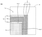
- FIGS. 1 is a cross-sectional view of the high-frequency module
- FIG. 2 is an enlarged view of a region A in FIG.
- the high-frequency module 1 a includes a wiring board 2, a plurality of components 3 a mounted on the upper surface 2 a of the wiring board 2, and each of the components provided on the upper surface 2 a of the wiring board 2.
- a mother substrate of an electronic device including a sealing resin layer 4a for sealing the component 3a and first and second shield layers 5 and 6 (corresponding to the “shield layer” of the present invention), for example, using a high-frequency signal Etc.
- the wiring board 2 is formed of, for example, a low-temperature co-fired ceramic or glass epoxy resin, and a plurality of land electrodes for mounting each component 3a are provided on the upper surface (corresponding to “one main surface of the wiring board” of the present invention). 7 is formed.
- ground electrodes 8a and 8b for grounding, various wiring electrodes (not shown), and a plurality of via conductors (not shown) are formed inside.
- the ground electrodes 8 a and 8 b are both provided so as to be exposed from the side surface 2 b of the wiring board 2.
- Each land electrode 7, ground electrodes 8a and 8b, and wiring electrodes are each formed of a metal generally employed as a wiring electrode such as Cu or Al.
- Each via conductor is formed of a metal such as Ag or Cu.
- Each land electrode 7 may be subjected to Ni / Au plating.
- each component 3a examples include semiconductor elements formed of semiconductors such as Si and GaAs, and chip components such as chip inductors, chip capacitors, and chip resistors. Each component 3a corresponds to a “first component” of the present invention.
- the sealing resin layer 4a (corresponding to the “first sealing resin layer” of the present invention) is provided so as to cover the upper surface 2a of the wiring board 2 and each component 3a.
- the sealing resin layer 4a can be formed of a resin generally employed as a sealing resin such as an epoxy resin.
- the first shield layer 5 is laminated on the sealing resin layer 4a so as to cover the surface 4a1 and the peripheral side surface 4a2 of the sealing resin layer 4a opposite to the upper surface 2a of the wiring substrate 2 and the side surface 2b of the wiring substrate 2.
- the first shield layer 5 includes an adhesion film 5a laminated on the surface of the sealing resin layer 4a, and a conductive film 5b laminated on the adhesion film 5a (“first conductivity of the present invention”). And a protective film 5c laminated on the conductive film 5b, and is electrically connected to the ground electrodes 8a and 8b exposed on the side surface 2b of the wiring board 2.
- the adhesion film 5a is provided to increase the adhesion strength between the conductive film 5b and the sealing resin layer 4a.
- the adhesion film 5a is electrically connected to the ground electrodes 8a and 8b exposed on the side surface 2b on the side surface 2b of the wiring board 2.
- the film thickness on the opposite surface 4a1 of the sealing resin layer 4a of the adhesion film 5a is preferably 0.01 ⁇ m or more and 0.5 ⁇ m or less.
- the adhesion film 5a is formed of SUS.
- the conductive film 5b is a layer that bears the substantial shielding function of the first shield layer 5, and can be formed of any metal of Cu, Ag, and Al, for example.
- the film thickness on the opposite surface 4a1 of the sealing resin layer 4a of the conductive film 5b is preferably 3 ⁇ m or more and 10 ⁇ m or less.
- the conductive film 5b is made of Cu.
- the thickness of the conductive film 5b is 3 ⁇ m or more, the conductive film 5b can effectively prevent noise from above the high-frequency module 1a from affecting each component 3a.
- the thickness of the conductive film 5b is 10 ⁇ m or less, the high-frequency module 1a can be reduced in height.
- the protective film 5c is provided to prevent the conductive film 5b from being corroded or scratched.
- SUS, Ti, Cr, Ni, TiCr, TiAl, NiAl, CrAl, CrNiAl It can be formed of any of the metals.
- the thickness of the sealing resin layer 4a of the protective film 5c on the opposite surface 4a1 is preferably 0.03 ⁇ m or more and 1.5 ⁇ m or less.
- the protective film 5c is made of SUS.
- the second shield layer 6 is provided to reinforce the first shield layer 5, and the first shield layer 5 covers the portion covering the peripheral side surface 4 a 2 of the sealing resin layer 4 a.
- a single shield layer 5 is laminated.
- the second shield layer 6 includes an adhesion film 6a laminated on a portion covering the peripheral side surface 4a2 of the sealing resin layer 4a of the protective film 5c, like the first shield layer 5.
- the conductive film 6b (corresponding to the “second conductive film” of the present invention) laminated on the adhesion film 6a and the protective film 6c laminated on the conductive film 6b are formed.
- the second shield layer 6 is provided so as to cover the peripheral side surface of the first shield layer 5 (protective film 5c), and the upper surface of the first shield layer 5 (protective film 5c) is covered. Not. Therefore, the 1st shield layer 5 is exposed to the part located on the said opposite surface 4a1 of the sealing resin layer 4a among the shield layers (the 1st shield layer 5 and the 2nd shield layer 6).
- the adhesion film 6a of the second shield layer 6 has the same configuration as the adhesion film 5a of the first shield layer 5, and the conductive film 6b of the second shield layer 6 has the same configuration as the conductive film 5b of the first shield layer 5.
- the protective film 6 c of the second shield layer 6 can be formed with the same configuration as the protective film 5 c of the first shield layer 5.
- each component 3a is mounted on the upper surface 2a of the wiring board 2 formed of low temperature co-fired ceramic (LTCC), glass epoxy resin or the like.
- the wiring board 2 is formed with electrodes such as land electrodes 7, ground electrodes 8a and 8b, and via conductors by a known method.
- Each component 3a can be mounted using a general surface mounting technique such as solder mounting. Note that flux cleaning may be performed after each component 3a is mounted.
- each component 3a is sealed with an epoxy resin to form a sealing resin layer 4a.
- the wiring substrate 2, the component 3a mounted on the upper surface 2a of the wiring substrate 2, the upper surface 2a of the wiring substrate 2, and each A mold structure having a sealing resin layer 4a laminated on the upper surface 2a of the wiring board 2 so as to cover the component 3a is prepared.
- the sealing resin layer 4a can be formed by a coating method, a printing method, a transfer mold method, a compression mold method, or the like.
- the surface 4a1 opposite to the upper surface 2a of the wiring substrate 2 of the sealing resin layer 4a may be ground.
- dry cleaning such as plasma etching may be performed before the formation of the sealing resin layer 4a.
- a release film at the time of resin sealing of each component 3a such as a transfer mold system and a compression mold system, you may use what roughened the resin contact surface of the said release film.
- the surface roughness Ra of the sealing resin layer 4a is preferably 1 ⁇ m or more and 10 ⁇ m or less.
- the high-frequency module 1a with a multi-piece collective board in which a plurality of wiring boards 2 are integrally formed
- individual molds are used by a dicer, a laser, a router, or the like. Divide into structures.
- the aggregate substrate may be half cut.
- the ground electrodes 8 a and 8 b formed on the wiring board 2 are exposed on the side surface 2 b of the wiring board 2 at the time of cutting.
- the mold structures after separation are arranged and supported on a sputtering tray.
- a paste or tape may be applied to the lower surface of the wiring board 2 in order to prevent the sputtered film from entering the lower surface of the wiring board 2.
- the tray on which the mold structure is set is disposed at a predetermined position in the chamber of the sputtering apparatus, and the chamber is evacuated. At this time, the tray is arranged so that the opposite surface 4a1 of the sealing resin layer 4a faces each target of the sputtering apparatus.
- the ultimate vacuum is low.
- the time required for evacuation is increased accordingly, so that the set ultimate vacuum is 1 ⁇ 10 ⁇ 3 Pa or more and 1 ⁇ 10 6 from the viewpoint of productivity. ⁇ 1 Pa or less is preferable.
- the chamber may be composed of a sputtering chamber and a load lock chamber (so-called front chamber).
- a sputtering apparatus an in-line type, a batch type, a single wafer type, or the like can be used.
- an adhesion film 5a of the first shield layer 5 is formed by sputtering so as to cover the surface of the sealing resin layer 4a and the side surface 2b of the wiring board 2.
- any one of SUS, Ti, Cr, Ni, TiCr, TiAl, NiAl, CrAl, and CrNiAl can be used as a target material.
- a voltage is applied to the SUS target for a desired time and sputtering is performed.
- the film thickness at this time (the film thickness of the portion of the adhesive film 5a located on the opposite surface 4a1 of the sealing resin layer 4a) is 0.01 ⁇ m or more and 0.5 ⁇ m or less.
- Ar gas used as a plasma source is used as a gas to be introduced into the chamber.
- the input amount at this time is set to 30 to 300 sccm, for example.
- pre-sputtering sin-called sputtering with the shutter closed
- a sintered target etc. can be used for a target other than a metal target.
- Some metal targets are difficult to form depending on the composition of the alloy, but in the case of sintered targets, the metal composition ratio can be adjusted with any composition, making it easy to optimize adhesion and corrosion resistance. It can be carried out.
- the power system of the sputtering apparatus can use a DC system, a pulse system, an RF system, or the like.
- the pulse method or the RF method even when a reaction product (oxide or nitride) is formed on the target surface and the resistance value is increased, the discharge can be stably performed.
- a conductive film 5b is formed on the surface of the adhesion film 5a by sputtering.
- any one of Cu, Ag, and Al can be used as a target material.
- sputtering is performed by applying a voltage to the Cu target for a desired time.
- Ar gas used as a plasma source is used as a gas to be introduced into the chamber.
- the input amount at this time is set to 30 to 300 sccm, for example.
- pre-sputtering may be performed on the Cu target.
- the film thickness on the peripheral side surface 4a2 of the sealing resin layer 4a in the conductive film 5b is the opposite surface 4a1. It becomes about 30% of the upper film thickness.
- the film thickness of the conductive film 5b is 3 ⁇ m or more and 10 ⁇ m or less on the opposite surface 4a1 of the sealing resin layer 4a
- the film thickness on the peripheral side surface 4a2 of the sealing resin layer 4a of the conductive film 5b is on the opposite surface 4a1.
- the conductive film 5b generally needs to have a thickness that is twice or more the high frequency skin depth ⁇ . Therefore, when the conductive film 5b is Cu, the thickness of the conductive film 5b needs to be about 2.7 ⁇ m in the 2.4 GHz band and about 1.8 ⁇ m in the 5 GHz band.
- the film thickness on the peripheral side surface 4a2 is about 0.9 ⁇ m.
- the film thickness on the opposite surface 4a1 of the sealing resin layer 4a of the conductive film 5b is 3 ⁇ m, and a sufficient shielding function is obtained.
- the film thickness on the peripheral side surface 4a2 of the sealing resin layer 4a of the conductive film 5b is about 0.9 ⁇ m, which is insufficient by about 2 ⁇ m to ensure a sufficient shielding function. Therefore, in this embodiment, the second shield layer 6 is formed to compensate for the shortage.
- the first shield layer 5 is completed by forming a protective film 5c on the surface of the conductive film 5b by sputtering in the same manner as the adhesion film 5a.
- a protective film 5c on the surface of the conductive film 5b by sputtering in the same manner as the adhesion film 5a.
- any one of SUS, Ti, Cr, Ni, TiCr, TiAl, NiAl, CrAl, and CrNiAl can be used as a target material.
- the film thickness of the protective film 5c at this time (the film thickness of the portion of the protective film 5c located on the opposite surface 4a1 of the sealing resin layer 4a) is 0.03 ⁇ m or more and 1.5 ⁇ m or less.
- the portions of the adhesion film 5a and the protective film 5c that are located on the peripheral side surface 4a2 of the sealing resin layer 4a have the thicknesses of the adhesion film 5a and the protective film 5c, respectively. It is about 30% of the portion located on the opposite surface 4a1 of the sealing resin layer 4a. Therefore, the film thickness of the portion located on the peripheral side surface 4a2 of the sealing resin layer 4a in the adhesion film 5a is, for example, 0.003 ⁇ m or more and 0.15 ⁇ m or less, and the periphery of the sealing resin layer 4a in the protective film 5c.
- the film thickness of the portion located on the side surface 4a2 is, for example, 0.009 ⁇ m or more and 0.45 ⁇ m or less.
- the conductive film 5b is a film that performs a substantial shielding function, and the shielding characteristics of the first shield layer 5 improve as the film thickness increases. In view of these circumstances, it is preferable that the thickness of each adhesion film 5a, conductive film 5b, and protective film 5c of the first shield layer 5 is the largest in the conductive film 5b and the smallest in the adhesion film 5a.
- first shield layer 5 covering the opposite surface 4a1 of the sealing resin layer 4a is masked with a tape or paste, and then the second shield layer 5 in the same manner as the adhesion film 5a of the first shield layer 5.
- An adhesion film 6a for the shield layer 6 is formed.
- a metal mask may be used as the mask.
- the conductive film 6 b of the second shield layer 6 is formed in the same manner as the conductive film 5 b of the first shield layer 5.
- the film thickness of the conductive film 6b at this time is preferably equal to or greater than the film thickness of the conductive film 5b of the first shield layer 5 (film thickness on the peripheral side surface 4a2 side of the sealing resin layer 4a).
- the protective film 6 c of the second shield layer 6 is formed in the same manner as the protective film 5 c of the first shield layer 5. Then, the high frequency module 1a is completed by taking out the tray from the sputtering apparatus and removing the mask.
- the adhesion film 6a, the conductive film 6b, and the protective film 6c of the second shield layer 6 are preferably formed of the same metal as the adhesion film 5a, the conductive film 5b, and the protective film 5c of the first shield layer 5, respectively.
- the manufacturing cost of the high-frequency module 1a can be reduced.
- the first shield layer 5 and the second shield layer 6 have the same configuration, the difference in thermal expansion coefficient between the shield layers 5 and 6 can be reduced. Peeling can be reduced.
- the 1st shield layer 5 and the 2nd shield layer 6 can be formed using a vacuum evaporation apparatus other than a sputtering device, for example.
- the first shield layer 5 provides desired shield characteristics. Even if it is a case where the thickness for obtaining cannot be ensured, the shortage can be secured by the second shield layer 6. Further, since the second shield layer 6 is not laminated on the side 4a1 opposite to the upper surface 2a of the wiring substrate 2 of the sealing resin layer 4a, only the first shield layer 5 is on the opposite surface 4a1 of the sealing resin layer 4a. Covered with. According to this configuration, it is possible to reduce the height of the high-frequency module 1a while ensuring desired shield characteristics.
- FIG. 3 is a partial cross-sectional view of the high-frequency module and corresponds to FIG.
- the high-frequency module 1b according to this embodiment differs from the high-frequency module 1a according to the first embodiment described with reference to FIGS. 1 and 2 in that the configuration of the second shield layer 60 is different as shown in FIG. That is. Since other configurations are the same as those of the high-frequency module 1a of the first embodiment, description thereof is omitted by attaching the same reference numerals.
- the second shield layer 60 is a magnetic film 60a (corresponding to the “third conductive film” of the present invention) laminated on a portion covering the peripheral side surface 4a2 of the sealing resin layer 4a of the first shield layer 5.
- the magnetic film 60 a is formed of a metal magnetic material having a relative permeability higher than that of the conductive film 5 b of the first shield layer 5.
- the relative permeability ⁇ s of metal Cu forming the conductive film 5 b of the first shield layer 5 is 0.999991
- the magnetic film 60a of the second shield layer 60 includes Ni having a relative permeability ⁇ s of 100 to 600, Permalloy having a relative permeability ⁇ s of 8000, Fe having a relative permeability ⁇ s of 5000, and the like. It is made of any metal.
- the magnetic film 60a of the second shield layer 60 is a metal having a relative permeability higher than that of Cu (for example, a relative permeability ⁇ s ⁇ What is necessary is just to be formed by 1).
- the protective film 60b can be formed with the same configuration as the protective film 5c of the first shield layer 5 such as, for example, formed of SUS.
- the conductive film 5b of the first shield layer 5 is formed of a metal magnetic material such as Ni, permalloy, and Fe, and the magnetic film 60a portion of the second shield layer 60 has a high conductivity such as Cu, Ag, and Al.
- the structure formed with the metal which it has may be sufficient. That is, the configuration of the conductive film 5b of the first shield layer 5 and the magnetic film 60a of the second shield layer 60 may be reversed.
- any one of the adhesion films 6a, the conductive films 6b, and the protective films 6c of the second shield layer 6 may be formed of a metal magnetic material such as Ni, permalloy, or Fe.
- the peripheral side surface 4a2 of the sealing resin layer 4a is covered with both the conductive film 5b having a high conductivity such as Cu and the magnetic film 60a having a high relative permeability.
- the shielding property against the magnetic field can be improved.
- the first shield layer 5 and the second shield layer can be obtained as compared with the configuration of the first embodiment in order to obtain a desired shield characteristic on the peripheral side surface 4a2 side of the sealing resin layer 4a.
- the total film thickness of 60 can be reduced. Therefore, the high-frequency module 1b can be reduced in height while the thickness of the first shield layer 5 and the second shield layer 60 on the peripheral side surface 4a2 side of the sealing resin layer 4a can be reduced. be able to.
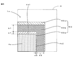
- FIG. 4 is a cross-sectional view of the high frequency module.
- the high-frequency module 1c according to this embodiment is different from the high-frequency module 1a according to the first embodiment described with reference to FIGS. 1 and 2 as shown in FIG. And the component 3b is covered with the sealing resin layer 4b, and the first shield layer 5 and the second shield layer 6 are The sealing resin layer 4b on the lower surface 2c side of the wiring board 2 is also covered. Since other configurations are the same as those of the high-frequency module 1a of the first embodiment, description thereof is omitted by attaching the same reference numerals.
- the component 3b (corresponding to the “second component” of the present invention) is a semiconductor element formed of a semiconductor such as Si or GaAs, a chip inductor, or a chip capacitor, like each component 3a on the upper surface 2a side of the wiring board 2. And chip components such as chip resistors.
- the encapsulating resin layer 4b (corresponding to the “second encapsulating resin layer” of the present invention and may be referred to as the second encapsulating resin layer 4b hereinafter) covers the lower surface 2c of the wiring board 2 and the component 3b. It is provided as follows.
- the sealing resin layer 4b is different from the sealing resin layer 4a (hereinafter sometimes referred to as the first sealing resin layer 4a) that covers the entire surface of the upper surface 2a of the wiring substrate 2, and the lower surface of the wiring substrate 2. Part of 2c is covered, and in this embodiment, the part not covered with the second sealing resin layer 4b is used as a space for connection to the outside of the high-frequency module 1c.
- the second sealing resin layer 4b may cover the entire lower surface 2c of the wiring board 2, or the first sealing resin layer 4a may also be a part of the wiring board 2 leaving a part of the upper surface 2a. You may make it coat
- the 2nd sealing resin layer 4b can be formed with resin generally employ
- the first shield layer 5 covers a part of the peripheral side surface 4b2 of the second sealing resin layer 4b in addition to the opposite surface 4a1 and the peripheral side surface 4a2 of the first sealing resin layer 4a.
- the second shield layer 6 includes a second sealing resin layer 4b in addition to a portion covering the peripheral side surface 4a2 of the first sealing resin layer 4a of the first shield layer 5 and a portion covering the side surface 2b of the wiring board 2.
- the surface 4b1 opposite to the lower surface 2c of the wiring board 2 and the portion of the peripheral side surface 4b2 of the second sealing resin layer 4b that is not covered with the first shield layer 5 are covered.
- the other configurations of the first shield layer 5 and the second shield layer 6 are the same as those in the first embodiment.
- the components 3a and 3b are mounted on the upper and lower surfaces 2a and 2c of the wiring substrate 2, and the components 3a and 3b on both surfaces 2a and 2c of the wiring substrate 2 are molded with the first and second sealing resin layers 4a and 4b.
- a mold structure is formed.
- the first sealing resin layer 4a molds the entire upper surface 2a of the wiring board 2
- the second sealing resin layer 4b is a part of the area where the component 3b of the lower surface 2c of the wiring board 2 is not mounted. Partially mold leaving part.
- Each of the first and second sealing resin layers 4a and 4b can be formed by a coating method, a printing method, a transfer molding method, a compression molding method, or the like.
- the first sealing resin layer 4a side that covers the entire upper surface 2a of the wiring substrate 2 is formed by a coating method or a compression molding method, and a second sealing resin that partially covers the lower surface 2c of the wiring substrate 2 is formed.
- the layer 4b side can also be formed by a transfer mold method.
- the formation method of the first shield layer 5 is the same as that of the high-frequency module 1a of the first embodiment, but the tray is disposed so that the opposite surface 4a1 of the first sealing resin layer 4a and each target of the sputtering apparatus face each other. Then, a part of the peripheral side surface 4b2 of the second sealing resin layer 4b is also covered with each adhesion film 5a, the conductive film 5b, and the protective film 5c of the first shield layer 5.
- the tray is taken out from the sputtering apparatus, the mold structure is turned over and set on the tray. A portion of the lower surface 2c of the wiring board 2 that does not require the formation of the second shield layer 6 is masked in advance using tape or paste. Then, a tray is again arranged in the sputtering apparatus, and the adhesion film 6a, the conductive film 6b, and the protective film 6c of the second shield layer 6 are formed in the same manner as the first shield layer 5. At this time, the tray is disposed so that the opposite surface 4b1 of the second sealing resin layer 4b faces each target.
- covers the surrounding side surface 4a2 of the 1st sealing resin layer 4a of the 1st shield layer 5
- covers the side surface 2b of the wiring board 2
- the second shield layer 6 covers each of the surface 4b1 opposite to the lower surface 2c and the portions of the peripheral side surface 4b2 of the second sealing resin layer 4b that are not covered by the first shield layer 5.
- the mold structure is turned over and film formation is performed twice, so that the side surfaces of the mold structure (the peripheral side surfaces 4a2 and 4b2 of the first and second sealing resin layers 4a and 4b and the wiring substrate 2)
- the side surface 2 b) can be covered with both the first shield layer 5 and the second shield layer 6.
- both the opposite surfaces 4a1 and 4b1 side of the first and second sealing resin layers 4a formed to be thicker than the peripheral side surfaces 4a2 and 4b2 are both the first shield layer 5 and the second shield layer 5a.
- the first and second sealing resin layers 4a and 4b, which are coated with only one of the shield layers 6, have the first shield layer 5 and the second shield layer on the side surfaces 4a2 and 4b2 of the thin sealing resin layers 4a and 4b. 6 are both coated. Therefore, it is possible to reduce the height of the high-frequency module 1c while ensuring the shielding characteristics on the side surfaces 4a2 and 4b2 of the first and second sealing resin layers 4a and 4b.
- FIG. 5 is a cross-sectional view of the high-frequency module.
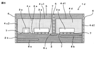
- the high-frequency module 1d according to this embodiment differs from the high-frequency module 1a according to the first embodiment described with reference to FIGS. 1 and 2 in that each component 3a has two seals as shown in FIG.
- the resin layers 4c and 4d are separately molded, the sealing resin layers 4c and 4d are individually covered with the first shield layer 5 and the second shield layer 6, and the wiring board 2 Is provided with another ground electrode 8c. Since other configurations are the same as those of the high-frequency module 1a of the first embodiment, description thereof is omitted by attaching the same reference numerals.
- the first shield layer 5 is opposite to the upper surface 2a of the sealing substrate 4c1 and the peripheral surface 4c2 opposite to the upper surface 2a of the wiring substrate 2 of one sealing resin layer 4c, and the upper surface 2a of the wiring substrate of the other sealing resin layer 4d.
- the surface 4d1, the peripheral side surface 4d2, and the side surface 2b of the wiring board 2 are covered.
- the second shield layer 6 includes a portion covering the peripheral side surface 4c2 of one sealing resin layer 4c of the first shield layer 5, a portion covering the peripheral side surface 4d2 of the other sealing resin layer 4d, and a side surface of the wiring board 2. It is laminated
- the first shield layer 5 and the second shield layer 6 are interposed between the sealing resin layers 4c and 4d.
- a portion of the first shield layer 5 located between both the sealing resin layers 4 c and 4 d is connected to a ground electrode 8 c formed on the wiring board 2.
- each of the sealing resin layers 4c and 4d corresponds to the “first sealing resin layer” of the present invention.
- each component 3a is collectively sealed with resin, a groove is formed between the predetermined components 3a using a laser or a dicer. Then, it can form by forming the 1st shield layer 5 and the 2nd shield layer 6 by the same method as the high frequency module 1a of 1st Embodiment.
- the first shield layer 5 and the second shield layer 6 are interposed between the sealing resin layers 4c and 4d, so that one of the seals is sealed. It is possible to prevent mutual interference of noise between the component 3a sealed in the stop resin layer 4c and the component 3a sealed in the other sealing resin layer 4d.
- FIG. 6 is a partial cross-sectional view of the high-frequency module, and corresponds to FIG.
- the high-frequency module 1e according to this embodiment differs from the high-frequency module 1a according to the first embodiment described with reference to FIGS. 1 and 2 in that the configuration of the third shield layer 50 is different as shown in FIG. That is. Since other configurations are the same as those of the high-frequency module 1a of the first embodiment, description thereof is omitted by attaching the same reference numerals.
- the third shield layer 50 has substantially the same three-layer structure as the first shield layer 5 of the first embodiment. Specifically, as shown in FIG. 6, the third shield layer 50 is formed of a sealing resin layer so as to cover the opposite surface 4a1 and peripheral side surface 4a2 of the sealing resin layer 4a and the side surface 2b of the wiring board 2. 4a, an adhesion film 50a laminated on the adhesion film 50a, a conductive film 50b laminated on the adhesion film 50a, and a protective film 50c laminated on the conductive film 50b.
- Each adhesion film 50a, conductive film 50b, and protective film 50c of the third shield layer 50 has the same configuration as each adhesion film 5a, conductive film 5b, and protective film 5c of the first shield layer 5.
- the ratio of the thickness a2 on the peripheral side surface 4a2 side to the thickness a1 on the opposite surface 4a1 side of the sealing resin layer 4a of the adhesion film 50a is the opposite surface of the sealing resin layer 4a of the conductive film 50b. It is formed to be smaller than the ratio of the thickness b2 on the peripheral side surface 4a2 side to the thickness b1 on the 4a1 side ((a2 / a1) ⁇ (b2 / b1)).
- the third shield layer 50 can be formed as follows, for example. Until the adhesion film 50a is formed, it is formed in the same manner as the high-frequency module 1a in the first embodiment, and the conductive film 50b is first in the same manner as the conductive film 5b in the first shield layer 5 in the first embodiment. Form a film. Thereafter, the tray is taken out from the sputtering apparatus, a mask is applied to the portion of the conductive film 5b that covers the opposite surface 4a1 of the sealing resin layer 4a, and the second conductive film 50b is formed again in the same manner. If it does so, a film thickness can be increased only in the part which coat
- the present invention is not limited to the above-described embodiments, and various modifications other than those described above can be made without departing from the spirit of the invention.
- membrane 6a of the 2nd shield layer 6 may be sufficient.
- the present invention can be applied to various high-frequency modules including a sealing resin layer that covers a component mounted on a wiring board and a shield layer laminated on the sealing resin layer.
Landscapes
- Engineering & Computer Science (AREA)
- Microelectronics & Electronic Packaging (AREA)
- Physics & Mathematics (AREA)
- Power Engineering (AREA)
- Condensed Matter Physics & Semiconductors (AREA)
- General Physics & Mathematics (AREA)
- Computer Hardware Design (AREA)
- Chemical & Material Sciences (AREA)
- Ceramic Engineering (AREA)
- Electromagnetism (AREA)
- Health & Medical Sciences (AREA)
- Toxicology (AREA)
- Materials Engineering (AREA)
- Mechanical Engineering (AREA)
- Metallurgy (AREA)
- Organic Chemistry (AREA)
- Chemical Kinetics & Catalysis (AREA)
- Inorganic Chemistry (AREA)
- Shielding Devices Or Components To Electric Or Magnetic Fields (AREA)
- Structures Or Materials For Encapsulating Or Coating Semiconductor Devices Or Solid State Devices (AREA)
Abstract
L'invention concerne un module à haute fréquence dont la hauteur peut être réduite, tout en assurant des caractéristiques de blindage. Ce module à haute fréquence (1a) comporte : une carte de circuit imprimé (2) ; un composant (3a) qui est monté sur une surface supérieure (2a) de la carte de circuit imprimé (2) ; une couche de résine d'étanchéité (4a) qui est stratifiée sur la surface supérieure (2a) de la carte de circuit imprimé (2) et qui scelle le composant (3a) ; une première couche de blindage (5) qui est stratifiée sur la couche de résine d'étanchéité (4a) afin de recouvrir une surface opposée (4a1), laquelle est située de l'autre côté de la surface de la couche de résine d'étanchéité (4a) sur le côté de la surface supérieure (2a) de la carte de circuit imprimé (2), et une surface latérale circonférentielle (4a2) de la première couche de résine d'étanchéité (4a) ; et une deuxième couche de blindage (6) qui est stratifiée sur une partie de la première couche de blindage (5), ladite partie recouvrant la surface latérale circonférentielle (4a2) de la couche de résine d'étanchéité (4a). Par conséquent, même dans les cas où la première couche de blindage (5) ne peut assurer l'épaisseur nécessaire à l'obtention de caractéristiques de blindage désirées, l'inconvénient est compensé par la deuxième couche de blindage (6), permettant ainsi de réduire la hauteur du module à haute fréquence (1a), tout en assurant des caractéristiques de blindage désirées.
Priority Applications (2)
| Application Number | Priority Date | Filing Date | Title |
|---|---|---|---|
| CN201680023133.8A CN107535078B (zh) | 2015-05-20 | 2016-05-17 | 高频模块 |
| US15/817,481 US10455748B2 (en) | 2015-05-20 | 2017-11-20 | High-frequency module |
Applications Claiming Priority (2)
| Application Number | Priority Date | Filing Date | Title |
|---|---|---|---|
| JP2015102674 | 2015-05-20 | ||
| JP2015-102674 | 2015-05-20 |
Related Child Applications (1)
| Application Number | Title | Priority Date | Filing Date |
|---|---|---|---|
| US15/817,481 Continuation US10455748B2 (en) | 2015-05-20 | 2017-11-20 | High-frequency module |
Publications (1)
| Publication Number | Publication Date |
|---|---|
| WO2016186103A1 true WO2016186103A1 (fr) | 2016-11-24 |
Family
ID=57320001
Family Applications (1)
| Application Number | Title | Priority Date | Filing Date |
|---|---|---|---|
| PCT/JP2016/064568 WO2016186103A1 (fr) | 2015-05-20 | 2016-05-17 | Module à haute fréquence |
Country Status (3)
| Country | Link |
|---|---|
| US (1) | US10455748B2 (fr) |
| CN (1) | CN107535078B (fr) |
| WO (1) | WO2016186103A1 (fr) |
Cited By (4)
| Publication number | Priority date | Publication date | Assignee | Title |
|---|---|---|---|---|
| JP2018088460A (ja) * | 2016-11-28 | 2018-06-07 | 株式会社村田製作所 | シールド層を有するモジュール |
| WO2020071492A1 (fr) * | 2018-10-05 | 2020-04-09 | 株式会社村田製作所 | Module |
| WO2020071493A1 (fr) * | 2018-10-05 | 2020-04-09 | 株式会社村田製作所 | Module |
| US10964645B2 (en) | 2017-02-28 | 2021-03-30 | Murata Manufacturing Co., Ltd. | Electronic component with thin-film shield layer |
Families Citing this family (17)
| Publication number | Priority date | Publication date | Assignee | Title |
|---|---|---|---|---|
| JP6511550B1 (ja) * | 2018-01-30 | 2019-05-15 | タツタ電線株式会社 | 電磁波シールドフィルム |
| WO2019159913A1 (fr) | 2018-02-15 | 2019-08-22 | 株式会社村田製作所 | Module haute fréquence |
| CN111771276B (zh) * | 2018-02-28 | 2023-12-26 | 株式会社村田制作所 | 高频模块 |
| JP6981537B2 (ja) * | 2018-03-20 | 2021-12-15 | 株式会社村田製作所 | 高周波モジュール |
| CN108990256A (zh) * | 2018-07-24 | 2018-12-11 | 苏州福莱盈电子有限公司 | 一种防止线路板信号泄漏的屏蔽方法 |
| US10804217B2 (en) | 2018-08-10 | 2020-10-13 | STATS ChipPAC Pte. Ltd. | EMI shielding for flip chip package with exposed die backside |
| US11355452B2 (en) | 2018-08-10 | 2022-06-07 | STATS ChipPAC Pte. Ltd. | EMI shielding for flip chip package with exposed die backside |
| US11309294B2 (en) * | 2018-09-05 | 2022-04-19 | Taiwan Semiconductor Manufacturing Company, Ltd. | Integrated fan-out packages and methods of forming the same |
| CN112673468B (zh) * | 2018-09-27 | 2024-05-03 | 株式会社村田制作所 | 模块及其制造方法 |
| US11071196B2 (en) * | 2019-04-05 | 2021-07-20 | Samsung Electro-Mechanics Co., Ltd. | Electronic device module and method of manufacturing electronic device module |
| WO2020250795A1 (fr) * | 2019-06-10 | 2020-12-17 | 株式会社ライジングテクノロジーズ | Dispositif de circuit électronique |
| WO2020250823A1 (fr) * | 2019-06-13 | 2020-12-17 | 株式会社村田製作所 | Module |
| WO2021006141A1 (fr) * | 2019-07-08 | 2021-01-14 | 株式会社村田製作所 | Module et son procédé de fabrication |
| US20220246446A1 (en) * | 2019-07-26 | 2022-08-04 | Nantong Tongfu Microelectronics Co., Ltd | Packaging structure and fabrication method thereof |
| KR102301208B1 (ko) * | 2019-08-14 | 2021-09-09 | 삼성전기주식회사 | 전자 소자 모듈 및 이를 구비하는 전자 기기 |
| CN112423462B (zh) * | 2019-08-20 | 2022-06-24 | 宏启胜精密电子(秦皇岛)有限公司 | 电路板 |
| CN113766096A (zh) * | 2020-06-05 | 2021-12-07 | 宁波舜宇光电信息有限公司 | 线路板、感光组件、摄像模组和感光组件的制备方法 |
Citations (4)
| Publication number | Priority date | Publication date | Assignee | Title |
|---|---|---|---|---|
| JPH0260297U (fr) * | 1988-10-25 | 1990-05-02 | ||
| JP2005276980A (ja) * | 2004-03-24 | 2005-10-06 | Matsushita Electric Ind Co Ltd | 回路部品内蔵モジュールの製造方法 |
| JP2006019342A (ja) * | 2004-06-30 | 2006-01-19 | Tdk Corp | 半導体ic内蔵基板 |
| JP2011159786A (ja) * | 2010-02-01 | 2011-08-18 | Panasonic Corp | モジュールとその製造方法 |
Family Cites Families (12)
| Publication number | Priority date | Publication date | Assignee | Title |
|---|---|---|---|---|
| DE10016867A1 (de) * | 2000-04-05 | 2001-10-18 | Epcos Ag | Bauelement mit Beschriftung |
| US7187060B2 (en) * | 2003-03-13 | 2007-03-06 | Sanyo Electric Co., Ltd. | Semiconductor device with shield |
| US7129422B2 (en) * | 2003-06-19 | 2006-10-31 | Wavezero, Inc. | EMI absorbing shielding for a printed circuit board |
| JP2007243122A (ja) | 2006-03-06 | 2007-09-20 | Be-Spputer Co Ltd | スパッタリング法によるシールド膜の成膜方法及び成膜されたシールド膜 |
| WO2011040030A1 (fr) | 2009-10-01 | 2011-04-07 | パナソニック株式会社 | Module et procédé de production associé |
| KR101855294B1 (ko) * | 2010-06-10 | 2018-05-08 | 삼성전자주식회사 | 반도체 패키지 |
| TW201213289A (en) * | 2010-07-29 | 2012-04-01 | Du Pont | Azeotropic and azeotrope-like compositions of methyl perfluoroheptene ethers and methanol and uses thereof |
| US9007273B2 (en) * | 2010-09-09 | 2015-04-14 | Advances Semiconductor Engineering, Inc. | Semiconductor package integrated with conformal shield and antenna |
| TWI460843B (zh) * | 2011-03-23 | 2014-11-11 | Universal Scient Ind Shanghai | 電磁屏蔽結構及其製作方法 |
| US9179538B2 (en) * | 2011-06-09 | 2015-11-03 | Apple Inc. | Electromagnetic shielding structures for selectively shielding components on a substrate |
| KR102161173B1 (ko) * | 2013-08-29 | 2020-09-29 | 삼성전자주식회사 | 패키지 온 패키지 장치 및 이의 제조 방법 |
| US9269673B1 (en) * | 2014-10-22 | 2016-02-23 | Advanced Semiconductor Engineering, Inc. | Semiconductor device packages |
-
2016
- 2016-05-17 WO PCT/JP2016/064568 patent/WO2016186103A1/fr active Application Filing
- 2016-05-17 CN CN201680023133.8A patent/CN107535078B/zh active Active
-
2017
- 2017-11-20 US US15/817,481 patent/US10455748B2/en active Active
Patent Citations (4)
| Publication number | Priority date | Publication date | Assignee | Title |
|---|---|---|---|---|
| JPH0260297U (fr) * | 1988-10-25 | 1990-05-02 | ||
| JP2005276980A (ja) * | 2004-03-24 | 2005-10-06 | Matsushita Electric Ind Co Ltd | 回路部品内蔵モジュールの製造方法 |
| JP2006019342A (ja) * | 2004-06-30 | 2006-01-19 | Tdk Corp | 半導体ic内蔵基板 |
| JP2011159786A (ja) * | 2010-02-01 | 2011-08-18 | Panasonic Corp | モジュールとその製造方法 |
Cited By (10)
| Publication number | Priority date | Publication date | Assignee | Title |
|---|---|---|---|---|
| JP2018088460A (ja) * | 2016-11-28 | 2018-06-07 | 株式会社村田製作所 | シールド層を有するモジュール |
| US10964645B2 (en) | 2017-02-28 | 2021-03-30 | Murata Manufacturing Co., Ltd. | Electronic component with thin-film shield layer |
| WO2020071492A1 (fr) * | 2018-10-05 | 2020-04-09 | 株式会社村田製作所 | Module |
| WO2020071493A1 (fr) * | 2018-10-05 | 2020-04-09 | 株式会社村田製作所 | Module |
| CN112740844A (zh) * | 2018-10-05 | 2021-04-30 | 株式会社村田制作所 | 模块 |
| JPWO2020071493A1 (ja) * | 2018-10-05 | 2021-09-02 | 株式会社村田製作所 | モジュール |
| JP7143896B2 (ja) | 2018-10-05 | 2022-09-29 | 株式会社村田製作所 | モジュール |
| US11646273B2 (en) | 2018-10-05 | 2023-05-09 | Murata Manufacturing Co., Ltd. | Module |
| CN112740844B (zh) * | 2018-10-05 | 2023-10-24 | 株式会社村田制作所 | 模块 |
| US11804448B2 (en) | 2018-10-05 | 2023-10-31 | Murata Manufacturing Co., Ltd. | Module |
Also Published As
| Publication number | Publication date |
|---|---|
| CN107535078A (zh) | 2018-01-02 |
| CN107535078B (zh) | 2020-03-31 |
| US20180077829A1 (en) | 2018-03-15 |
| US10455748B2 (en) | 2019-10-22 |
Similar Documents
| Publication | Publication Date | Title |
|---|---|---|
| WO2016186103A1 (fr) | Module à haute fréquence | |
| WO2016204208A1 (fr) | Module et son procédé de fabrication | |
| WO2019117073A1 (fr) | Substrat de câblage en verre et son procédé de fabrication, et dispositif à semi-conducteurs | |
| JP6512298B2 (ja) | 高周波モジュールおよびその製造方法 | |
| US8389866B2 (en) | Resin circuit board | |
| JP2017103423A (ja) | 電子部品および電子部品の製造方法 | |
| US10770223B2 (en) | High frequency component | |
| US20190341352A1 (en) | Tapered corner package for emi shield | |
| JP6981537B2 (ja) | 高周波モジュール | |
| TWI507119B (zh) | 柔性電路板及其製作方法 | |
| US20070264496A1 (en) | Solderable Plastic EMI Shielding | |
| JPH03225810A (ja) | 積層型コンデンサーにおける端子電極膜の構造及び端子電極膜の形成方法 | |
| US6248958B1 (en) | Resistivity control of CIC material | |
| US10861683B2 (en) | Vacuum device | |
| JP2010109044A (ja) | 配線基板及びこれを用いたプローブカード | |
| JP6884062B2 (ja) | 配線基板 | |
| KR102044235B1 (ko) | 전자부품의 제조 방법 및 성막 장치 | |
| TW202118887A (zh) | 間隙配置構件 | |
| WO2022044515A1 (fr) | Composant électronique haute fréquence et module | |
| WO2022044516A1 (fr) | Composant électronique haute fréquence | |
| JPH03129894A (ja) | フレキシブルプリント配線板およびその製造方法 | |
| JP2023148866A (ja) | コイル部品、回路基板、電子機器およびコイル部品の製造方法 | |
| JP2006196483A (ja) | 配線基板及びその製造方法 | |
| JPH06112083A (ja) | 薄膜コンデンサ | |
| WO2013024837A1 (fr) | Procédé de fabrication de composant et composant |
Legal Events
| Date | Code | Title | Description |
|---|---|---|---|
| 121 | Ep: the epo has been informed by wipo that ep was designated in this application |
Ref document number: 16796496 Country of ref document: EP Kind code of ref document: A1 |
|
| NENP | Non-entry into the national phase |
Ref country code: DE |
|
| 122 | Ep: pct application non-entry in european phase |
Ref document number: 16796496 Country of ref document: EP Kind code of ref document: A1 |
|
| NENP | Non-entry into the national phase |
Ref country code: JP |