WO2016170978A1 - 半導体装置 - Google Patents
半導体装置 Download PDFInfo
- Publication number
- WO2016170978A1 WO2016170978A1 PCT/JP2016/061206 JP2016061206W WO2016170978A1 WO 2016170978 A1 WO2016170978 A1 WO 2016170978A1 JP 2016061206 W JP2016061206 W JP 2016061206W WO 2016170978 A1 WO2016170978 A1 WO 2016170978A1
- Authority
- WO
- WIPO (PCT)
- Prior art keywords
- semiconductor substrate
- protective film
- semiconductor device
- active region
- region
- Prior art date
- Legal status (The legal status is an assumption and is not a legal conclusion. Google has not performed a legal analysis and makes no representation as to the accuracy of the status listed.)
- Ceased
Links
Images






Classifications
-
- H—ELECTRICITY
- H10—SEMICONDUCTOR DEVICES; ELECTRIC SOLID-STATE DEVICES NOT OTHERWISE PROVIDED FOR
- H10D—INORGANIC ELECTRIC SEMICONDUCTOR DEVICES
- H10D62/00—Semiconductor bodies, or regions thereof, of devices having potential barriers
- H10D62/10—Shapes, relative sizes or dispositions of the regions of the semiconductor bodies; Shapes of the semiconductor bodies
- H10D62/102—Constructional design considerations for preventing surface leakage or controlling electric field concentration
- H10D62/103—Constructional design considerations for preventing surface leakage or controlling electric field concentration for increasing or controlling the breakdown voltage of reverse-biased devices
- H10D62/105—Constructional design considerations for preventing surface leakage or controlling electric field concentration for increasing or controlling the breakdown voltage of reverse-biased devices by having particular doping profiles, shapes or arrangements of PN junctions; by having supplementary regions, e.g. junction termination extension [JTE]
-
- H—ELECTRICITY
- H10—SEMICONDUCTOR DEVICES; ELECTRIC SOLID-STATE DEVICES NOT OTHERWISE PROVIDED FOR
- H10D—INORGANIC ELECTRIC SEMICONDUCTOR DEVICES
- H10D12/00—Bipolar devices controlled by the field effect, e.g. insulated-gate bipolar transistors [IGBT]
- H10D12/01—Manufacture or treatment
- H10D12/031—Manufacture or treatment of IGBTs
-
- H—ELECTRICITY
- H10—SEMICONDUCTOR DEVICES; ELECTRIC SOLID-STATE DEVICES NOT OTHERWISE PROVIDED FOR
- H10D—INORGANIC ELECTRIC SEMICONDUCTOR DEVICES
- H10D12/00—Bipolar devices controlled by the field effect, e.g. insulated-gate bipolar transistors [IGBT]
- H10D12/411—Insulated-gate bipolar transistors [IGBT]
- H10D12/441—Vertical IGBTs
-
- H—ELECTRICITY
- H10—SEMICONDUCTOR DEVICES; ELECTRIC SOLID-STATE DEVICES NOT OTHERWISE PROVIDED FOR
- H10D—INORGANIC ELECTRIC SEMICONDUCTOR DEVICES
- H10D30/00—Field-effect transistors [FET]
- H10D30/60—Insulated-gate field-effect transistors [IGFET]
-
- H—ELECTRICITY
- H10—SEMICONDUCTOR DEVICES; ELECTRIC SOLID-STATE DEVICES NOT OTHERWISE PROVIDED FOR
- H10D—INORGANIC ELECTRIC SEMICONDUCTOR DEVICES
- H10D30/00—Field-effect transistors [FET]
- H10D30/60—Insulated-gate field-effect transistors [IGFET]
- H10D30/64—Double-diffused metal-oxide semiconductor [DMOS] FETs
- H10D30/66—Vertical DMOS [VDMOS] FETs
- H10D30/665—Vertical DMOS [VDMOS] FETs having edge termination structures
-
- H—ELECTRICITY
- H10—SEMICONDUCTOR DEVICES; ELECTRIC SOLID-STATE DEVICES NOT OTHERWISE PROVIDED FOR
- H10D—INORGANIC ELECTRIC SEMICONDUCTOR DEVICES
- H10D62/00—Semiconductor bodies, or regions thereof, of devices having potential barriers
- H10D62/10—Shapes, relative sizes or dispositions of the regions of the semiconductor bodies; Shapes of the semiconductor bodies
- H10D62/102—Constructional design considerations for preventing surface leakage or controlling electric field concentration
- H10D62/103—Constructional design considerations for preventing surface leakage or controlling electric field concentration for increasing or controlling the breakdown voltage of reverse-biased devices
- H10D62/104—Constructional design considerations for preventing surface leakage or controlling electric field concentration for increasing or controlling the breakdown voltage of reverse-biased devices having particular shapes of the bodies at or near reverse-biased junctions, e.g. having bevels or moats
-
- H—ELECTRICITY
- H10—SEMICONDUCTOR DEVICES; ELECTRIC SOLID-STATE DEVICES NOT OTHERWISE PROVIDED FOR
- H10D—INORGANIC ELECTRIC SEMICONDUCTOR DEVICES
- H10D62/00—Semiconductor bodies, or regions thereof, of devices having potential barriers
- H10D62/10—Shapes, relative sizes or dispositions of the regions of the semiconductor bodies; Shapes of the semiconductor bodies
- H10D62/102—Constructional design considerations for preventing surface leakage or controlling electric field concentration
- H10D62/103—Constructional design considerations for preventing surface leakage or controlling electric field concentration for increasing or controlling the breakdown voltage of reverse-biased devices
- H10D62/105—Constructional design considerations for preventing surface leakage or controlling electric field concentration for increasing or controlling the breakdown voltage of reverse-biased devices by having particular doping profiles, shapes or arrangements of PN junctions; by having supplementary regions, e.g. junction termination extension [JTE]
- H10D62/106—Constructional design considerations for preventing surface leakage or controlling electric field concentration for increasing or controlling the breakdown voltage of reverse-biased devices by having particular doping profiles, shapes or arrangements of PN junctions; by having supplementary regions, e.g. junction termination extension [JTE] having supplementary regions doped oppositely to or in rectifying contact with regions of the semiconductor bodies, e.g. guard rings with PN or Schottky junctions
-
- H—ELECTRICITY
- H10—SEMICONDUCTOR DEVICES; ELECTRIC SOLID-STATE DEVICES NOT OTHERWISE PROVIDED FOR
- H10D—INORGANIC ELECTRIC SEMICONDUCTOR DEVICES
- H10D62/00—Semiconductor bodies, or regions thereof, of devices having potential barriers
- H10D62/10—Shapes, relative sizes or dispositions of the regions of the semiconductor bodies; Shapes of the semiconductor bodies
- H10D62/113—Isolations within a component, i.e. internal isolations
- H10D62/115—Dielectric isolations, e.g. air gaps
-
- H—ELECTRICITY
- H10—SEMICONDUCTOR DEVICES; ELECTRIC SOLID-STATE DEVICES NOT OTHERWISE PROVIDED FOR
- H10D—INORGANIC ELECTRIC SEMICONDUCTOR DEVICES
- H10D62/00—Semiconductor bodies, or regions thereof, of devices having potential barriers
- H10D62/80—Semiconductor bodies, or regions thereof, of devices having potential barriers characterised by the materials
- H10D62/83—Semiconductor bodies, or regions thereof, of devices having potential barriers characterised by the materials being Group IV materials, e.g. B-doped Si or undoped Ge
- H10D62/832—Semiconductor bodies, or regions thereof, of devices having potential barriers characterised by the materials being Group IV materials, e.g. B-doped Si or undoped Ge being Group IV materials comprising two or more elements, e.g. SiGe
- H10D62/8325—Silicon carbide
-
- H—ELECTRICITY
- H10—SEMICONDUCTOR DEVICES; ELECTRIC SOLID-STATE DEVICES NOT OTHERWISE PROVIDED FOR
- H10D—INORGANIC ELECTRIC SEMICONDUCTOR DEVICES
- H10D62/00—Semiconductor bodies, or regions thereof, of devices having potential barriers
- H10D62/80—Semiconductor bodies, or regions thereof, of devices having potential barriers characterised by the materials
- H10D62/85—Semiconductor bodies, or regions thereof, of devices having potential barriers characterised by the materials being Group III-V materials, e.g. GaAs
-
- H—ELECTRICITY
- H10—SEMICONDUCTOR DEVICES; ELECTRIC SOLID-STATE DEVICES NOT OTHERWISE PROVIDED FOR
- H10D—INORGANIC ELECTRIC SEMICONDUCTOR DEVICES
- H10D64/00—Electrodes of devices having potential barriers
- H10D64/20—Electrodes characterised by their shapes, relative sizes or dispositions
- H10D64/27—Electrodes not carrying the current to be rectified, amplified, oscillated or switched, e.g. gates
- H10D64/311—Gate electrodes for field-effect devices
- H10D64/411—Gate electrodes for field-effect devices for FETs
- H10D64/511—Gate electrodes for field-effect devices for FETs for IGFETs
- H10D64/517—Gate electrodes for field-effect devices for FETs for IGFETs characterised by the conducting layers
- H10D64/519—Gate electrodes for field-effect devices for FETs for IGFETs characterised by the conducting layers characterised by their top-view geometrical layouts
-
- H—ELECTRICITY
- H10—SEMICONDUCTOR DEVICES; ELECTRIC SOLID-STATE DEVICES NOT OTHERWISE PROVIDED FOR
- H10D—INORGANIC ELECTRIC SEMICONDUCTOR DEVICES
- H10D64/00—Electrodes of devices having potential barriers
- H10D64/60—Electrodes characterised by their materials
- H10D64/62—Electrodes ohmically coupled to a semiconductor
-
- H—ELECTRICITY
- H10—SEMICONDUCTOR DEVICES; ELECTRIC SOLID-STATE DEVICES NOT OTHERWISE PROVIDED FOR
- H10W—GENERIC PACKAGES, INTERCONNECTIONS, CONNECTORS OR OTHER CONSTRUCTIONAL DETAILS OF DEVICES COVERED BY CLASS H10
- H10W20/00—Interconnections in chips, wafers or substrates
- H10W20/40—Interconnections external to wafers or substrates, e.g. back-end-of-line [BEOL] metallisations or vias connecting to gate electrodes
- H10W20/41—Interconnections external to wafers or substrates, e.g. back-end-of-line [BEOL] metallisations or vias connecting to gate electrodes characterised by their conductive parts
- H10W20/44—Conductive materials thereof
- H10W20/4403—Conductive materials thereof based on metals, e.g. alloys, metal silicides
-
- H—ELECTRICITY
- H10—SEMICONDUCTOR DEVICES; ELECTRIC SOLID-STATE DEVICES NOT OTHERWISE PROVIDED FOR
- H10W—GENERIC PACKAGES, INTERCONNECTIONS, CONNECTORS OR OTHER CONSTRUCTIONAL DETAILS OF DEVICES COVERED BY CLASS H10
- H10W20/00—Interconnections in chips, wafers or substrates
- H10W20/40—Interconnections external to wafers or substrates, e.g. back-end-of-line [BEOL] metallisations or vias connecting to gate electrodes
- H10W20/45—Interconnections external to wafers or substrates, e.g. back-end-of-line [BEOL] metallisations or vias connecting to gate electrodes characterised by their insulating parts
- H10W20/47—Interconnections external to wafers or substrates, e.g. back-end-of-line [BEOL] metallisations or vias connecting to gate electrodes characterised by their insulating parts comprising two or more dielectric layers having different properties, e.g. different dielectric constants
-
- H—ELECTRICITY
- H10—SEMICONDUCTOR DEVICES; ELECTRIC SOLID-STATE DEVICES NOT OTHERWISE PROVIDED FOR
- H10D—INORGANIC ELECTRIC SEMICONDUCTOR DEVICES
- H10D62/00—Semiconductor bodies, or regions thereof, of devices having potential barriers
- H10D62/10—Shapes, relative sizes or dispositions of the regions of the semiconductor bodies; Shapes of the semiconductor bodies
- H10D62/17—Semiconductor regions connected to electrodes not carrying current to be rectified, amplified or switched, e.g. channel regions
- H10D62/393—Body regions of DMOS transistors or IGBTs
-
- H—ELECTRICITY
- H10—SEMICONDUCTOR DEVICES; ELECTRIC SOLID-STATE DEVICES NOT OTHERWISE PROVIDED FOR
- H10D—INORGANIC ELECTRIC SEMICONDUCTOR DEVICES
- H10D62/00—Semiconductor bodies, or regions thereof, of devices having potential barriers
- H10D62/80—Semiconductor bodies, or regions thereof, of devices having potential barriers characterised by the materials
- H10D62/85—Semiconductor bodies, or regions thereof, of devices having potential barriers characterised by the materials being Group III-V materials, e.g. GaAs
- H10D62/8503—Nitride Group III-V materials, e.g. AlN or GaN
-
- H—ELECTRICITY
- H10—SEMICONDUCTOR DEVICES; ELECTRIC SOLID-STATE DEVICES NOT OTHERWISE PROVIDED FOR
- H10W—GENERIC PACKAGES, INTERCONNECTIONS, CONNECTORS OR OTHER CONSTRUCTIONAL DETAILS OF DEVICES COVERED BY CLASS H10
- H10W74/00—Encapsulations, e.g. protective coatings
- H10W74/10—Encapsulations, e.g. protective coatings characterised by their shape or disposition
- H10W74/131—Encapsulations, e.g. protective coatings characterised by their shape or disposition the semiconductor body being only partially enclosed
- H10W74/137—Encapsulations, e.g. protective coatings characterised by their shape or disposition the semiconductor body being only partially enclosed the encapsulations being directly on the semiconductor body
Definitions
- the present invention relates to a semiconductor device.
- a barrier metal layer has been provided in order to prevent corrosion of an interlayer insulating film caused by aluminum (Al) in a source electrode and short circuit between a gate electrode and a source electrode formed of polysilicon.
- Al aluminum
- a barrier metal layer has been provided between the anode and cathode electrodes having Al and the polysilicon layer (see, for example, Patent Document 1).
- Patent Literature [Patent Document 1] JP 2012-129503 A [Non-Patent Document] [Non-Patent Document 1] K.
- Non-Patent Document 2 B. Jayant Baliga, Silicon Carbide Power Devices (USA), World Scientific Publishing Company 6 (World Scientific Publishing Co., Ltd. 6). March 30, p. 61
- a semiconductor device including a semiconductor substrate, a first lower insulating film, and a first protective film.
- the semiconductor substrate may have an active region and a breakdown voltage structure.
- the breakdown voltage structure may be provided around the active region.
- the first lower insulating film may be provided in the breakdown voltage structure portion on the semiconductor substrate.
- the first protective film may be provided on the first lower insulating film.
- the first protective film may be electrically insulated from the semiconductor substrate.
- the first protective film may occlude hydrogen.
- the semiconductor substrate may be of the first conductivity type.
- the semiconductor substrate may have a second conductivity type region on the front surface of the pressure-resistant structure portion.
- the first protective film may cover at least the upper portion of the second conductivity type region.
- the region of the second conductivity type may have a region where the concentration decreases in the direction from the active region toward the breakdown voltage structure.
- the first protective film provided in the breakdown voltage structure portion may be electrically isolated from the active region.
- the semiconductor device may further include a first upper insulating film on the first protective film provided in the breakdown voltage structure.
- the first protective film may be integrally formed in the pressure resistant structure.
- the semiconductor substrate may further include a step portion having an inclined portion and a flat portion in the pressure-resistant structure portion.
- the first protective film may be provided so as to cover the entire upper portion of the semiconductor substrate including the stepped portion in the breakdown voltage structure portion.
- the semiconductor device may further include a gate runner part and a gate pad part.
- the gate runner part may be provided between the active region and the breakdown voltage structure part.
- the gate pad part may be provided between the active region and the gate runner part.
- the gate runner part and the gate pad part may have a second lower insulating film and a second protective film.
- the second lower insulating film may be provided on the semiconductor substrate.
- the second protective film may be provided on the second lower insulating film.
- the second protective film may occlude hydrogen.
- the active region may further include a third lower insulating film and a third protective film.
- the third lower insulating film may be provided on the semiconductor substrate.
- the third protective film may be provided on the third lower insulating film.
- the third protective film may occlude hydrogen.
- the active region may further include a contact portion.
- the contact portion may provide electrical connection between the semiconductor substrate and the third protective film.
- the third protective film may be provided on the semiconductor substrate.
- the semiconductor substrate may have at least nickel silicide.
- the third protective film may include at least titanium carbide.
- the thickness of the first protective film in the pressure-resistant structure portion may be larger than the thickness of the third protective film in the active region.
- the thickness of the third protective film in the active region may be larger than the thickness of the first protective film in the breakdown voltage structure.
- FIG. 1 is a plan view of a semiconductor device 100.
- FIG. It is a figure which shows the AA cross section in FIG. It is a figure which shows the BB cross section in FIG. It is a figure which shows CC cross section in FIG. It is a figure which shows the gate threshold value (Vth) variation
- Vth gate threshold value
- change_quantity with respect to gate bias application time It is a figure which shows the process of forming the drift layer 12 and several p-type area
- FIG. 6 is a diagram showing a process of forming a source region 26 and a contact region 28. It is a figure which shows the process of forming the insulating film.
- Vth gate threshold value
- FIG. 5 is a diagram showing a stage of forming a gate insulating film 32, a gate electrode 34, an interlayer insulating film 36, and an interlayer insulating film 52. It is a figure which shows the step which forms the titanium film and the metal layer. It is a figure which shows the step which forms the passivation film 54 and the drain electrode 62.
- n or p means that electrons or holes are majority carriers, respectively.
- + means that the impurity concentration is higher than that not described
- ⁇ means that the impurity concentration is lower than that not described.
- the first conductivity type means n-type and the second conductivity type means p-type. In other examples, the first conductivity type means p-type and the second conductivity type means p-type. Two conductivity types may mean n-type.
- FIG. 1 is a plan view of the semiconductor device 100. That is, FIG. 1 is a diagram showing a case where the semiconductor substrate 10 is viewed from the top.
- the semiconductor device 100 has a plane parallel to the xy plane.
- the x direction and the y direction are directions perpendicular to each other, and the z direction is a direction perpendicular to the xy plane.
- the front surface side means the + z direction side of an object having a surface parallel to the xy plane
- the back surface side means the ⁇ z direction side of the object.
- a surface located between the front surface side and the back surface side of the object is referred to as a side surface of the object.
- the front surface of the semiconductor substrate 10 is referred to as a front surface 14, and the back surface of the semiconductor substrate 10 is referred to as a back surface 16.
- the semiconductor device 100 has a semiconductor substrate 10.
- the semiconductor substrate 10 is provided with an active region 101 and a breakdown voltage structure 102.
- the breakdown voltage structure 102 is provided around the active region 101. Note that “a” is provided around b in the semiconductor device 100 means that “b” is provided surrounding “a” when the semiconductor device 100 is viewed from above.
- the active region 101 in this example is a region having a vertical MOSFET (Metal Oxide Semiconductor Field Effect Transistor).
- the active region 101 may have an IGBT (Insulated Gate Bipolar Transistor) instead of the vertical MOSFET.
- the withstand voltage structure portion 102 is a portion having a function of relaxing or dispersing the electric field concentration at the end portion of the semiconductor substrate 10.
- the semiconductor substrate 10 has a JTE (Junction Termination Extension) structure, which will be described later, in the breakdown voltage structure portion 102.
- the JTE structure has a JTE high concentration region 37 and a JTE low concentration region 38, which will be described later, provided around the active region 101.
- the semiconductor device 100 further includes a gate runner unit 103 and a gate pad unit 105.
- the gate runner portion 103 is provided between the active region 101 and the breakdown voltage structure portion 102 when the semiconductor device 100 is viewed from above.
- the gate runner portion 103 is provided around the active region 101.
- the gate runner portion 103 is a wiring electrically connected to a gate electrode 34 described later.
- the gate pad portion 105 is provided between the active region 101 and the gate runner portion 103 when the semiconductor device 100 is viewed from above.
- the gate pad portion 105 is provided in electrical connection with the gate runner portion 103.
- the gate pad portion 105 is a portion protruding from the gate runner portion 103 to the active region 101.
- the gate pad portion 105 provides electrical connection to external wiring.
- the gate terminal wiring is connected to the gate pad portion 105 by wire bonding.
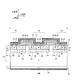
- FIG. 2 is a diagram showing an AA cross section in FIG. FIG. 2 is a view showing a cross section of the active region 101.
- the semiconductor substrate 10 of this example has silicon carbide (SiC).
- the semiconductor substrate 10 may be another wide gap semiconductor material.
- the semiconductor substrate 10 includes gallium nitride (GaN).
- the semiconductor substrate 10 is the first conductivity type.
- the semiconductor substrate 10 has an n + -type first conductivity type layer 11 on the back surface 16 side and an n-type drift layer 12 on the front surface 14 side.
- the semiconductor substrate 10 has a p-type well region 22, a p-type base region 24, an n + -type source region 26, and a p + -type contact region 28 on the front surface 14 side of the drift layer 12.
- the base region 24 is provided under the gate electrode 34.
- “upper” or “upper” refers to a direction from the back surface 16 of the semiconductor substrate 10 toward the front surface 14.
- “down” or “down” refers to a direction from the front surface 14 to the back surface 16 of the semiconductor substrate 10.
- the base region 24 functions as a channel formation region. When an electric field is applied from the gate electrode 34 through the gate insulating film 32, a channel is formed in a part of the base region 24.
- the n + -type source region 26 is provided in the base region 24 so as to be sandwiched or surrounded by the base region 24.
- the p + -type contact region 28 is provided in the base region 24 so as to be sandwiched or surrounded by the source region 26.
- the p + -type contact region 28 has a function of reducing contact resistance with the source electrode.
- the gate insulating film 32 electrically isolates at least the base region 24 and the gate electrode 34.
- the gate insulating film 32 in this example is provided in contact with the base region 24 and the source region 26 on the front surface 14.
- the gate electrode 34 is provided on the gate insulating film 32.
- An interlayer insulating film 36 as a third lower insulating layer is located on the gate electrode 34.
- the interlayer insulating film 36 is provided so as to surround the front surface side and the side surface of the gate electrode 34.
- the interlayer insulating film 36 may be a PSG (Phosphosilicate Glass) film or a BPSG (Borophosphosilicate Glass) film.
- a titanium (Ti) film 42 as a third protective film is provided on the interlayer insulating film 36.
- the titanium film 42 has a function of storing hydrogen.
- the titanium film 42 may contain titanium silicide (TiSix).
- the metal layer 44 is provided on the titanium film 42.
- the metal layer 44 may be aluminum (Al) or an aluminum alloy such as aluminum silicide (AlSi) containing 1% by weight of silicon (Si).
- AlSi aluminum silicide
- the titanium film 42 and the metal layer 44 function as a source electrode in the active region 101.
- a drain electrode 62 is provided under the back surface 16 of the semiconductor substrate 10.
- the contact portion 30 is a region where the titanium film 42 contacts the source region 26 and the contact region 28.
- the contact portion 30 provides electrical connection between the semiconductor substrate 10 and the titanium film 42.
- a part of the source region 26 and the contact region 28 have a nickel silicide (NiSi) region 29.
- the titanium film 42 has at least a titanium carbide (TiC) region 43.
- FIG. 3 is a view showing a BB cross section in FIG.
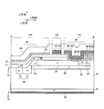
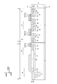
- FIG. 3 is a view showing a cross section across the end portion of the active region 101, the gate runner portion 103, and the pressure-resistant structure portion 102.
- a stacked body of the insulating film 51 and the interlayer insulating film 52 is provided from the outer peripheral end portion of the active region 101 to the outer peripheral end portion of the breakdown voltage structure portion 102.
- the insulating film 51 may be an oxide film such as silicon oxide (SiO 2 ), PSG, or BPSG.
- the interlayer insulating film 52 may be the same material as the interlayer insulating film 36.
- the interlayer insulating film 52 may be PSG or BPSG.
- the gate runner portion 103 includes an interlayer insulating film 52 as a second lower insulating film, a titanium film 42 as a second protective film, and a metal layer 44.
- the titanium film 42 is provided on the interlayer insulating film 52.
- the titanium film 42 occludes hydrogen.
- active hydrogen can be prevented from entering the semiconductor substrate 10 not only in the active region 101 but also in the gate runner portion 103.
- the withstand voltage structure 102 has at least an interlayer insulating film 52 as a first lower insulating film and a titanium film 42 as a first protective film.
- the first to third protective films in this example are the titanium films 42. Since the titanium film 42 of the breakdown voltage structure 102 is provided on the interlayer insulating film 52, it is electrically insulated from the semiconductor substrate 10.
- a titanium film 42 that occludes hydrogen is also provided in the pressure-resistant structure 102.
- active hydrogen can be prevented from entering the semiconductor substrate 10 from the pressure-resistant structure 102. Therefore, the gate threshold value of the active region 101 can be prevented from changing.
- a passivation film 54 as a first upper insulating film is provided on the titanium film 42 of the pressure-resistant structure 102.
- the passivation film 54 is provided at the uppermost position in the active region 101, the breakdown voltage structure portion 102, and the gate runner portion 103. In the active region 101 and the gate pad portion 105, the passivation film 54 is partially removed to ensure electrical continuity with the outside.
- the titanium film 42 of the pressure resistant structure 102 has a floating potential.
- the titanium film 42 provided in the breakdown voltage structure 102 is electrically isolated from the active region 101.
- the titanium film 42 of the breakdown voltage structure portion 102 is also electrically separated from the gate runner portion 103.
- the separation distance of the titanium film 42 between the pressure-resistant structure portion 102 and the gate runner portion 103 may be 2 ⁇ m or more and 10 ⁇ m or less.
- the separation distance of the titanium film 42 between the active region 101 and the gate runner portion 103 may also be 2 ⁇ m or more and 10 ⁇ m or less.
- the semiconductor substrate 10 has a step 45 in the pressure-resistant structure 102.
- the step portion 45 includes two flat portions 46 having different height positions in the z direction and an inclined portion 47 between the two flat portions 46.
- a second conductivity type region 39 is provided in the flat portion 46 positioned below the two flat portions 46. Since the titanium film 42 has a floating potential, no voltage is applied to the second conductivity type region 39. Therefore, the breakdown voltage structure 102 can function as a JTE structure, not a field plate structure. Thereby, it is possible to prevent the insulation film 51 and the interlayer insulation film 52 from being broken down.
- the semiconductor substrate 10 has a JTE high-concentration region 37 and a JTE low-concentration region 38 as the second conductivity type region 39 on the front surface 14 of the breakdown voltage structure 102.
- the JTE low concentration region 38 has a lower p-type impurity concentration than the JTE high concentration region 37.
- the JTE high concentration region 37 of this example has a p-type impurity
- the JTE low concentration region 38 has a p ⁇ type impurity. That is, the second conductivity type region 39 is a region where the concentration of the p-type impurity decreases in the direction from the active region 101 toward the breakdown voltage structure 102.
- the titanium film 42 is integrally formed in the pressure resistant structure 102.
- the titanium film 42 being formed integrally means that the titanium film 42 is a solid film. For example, this means that no holes or openings are formed in the titanium film 42 in the pressure-resistant structure 102.
- the titanium film 42 covers at least the upper side of the second conductivity type region 39 in the breakdown voltage structure 102.
- the titanium film 42 of this example is provided so as to cover the entire upper portion of the semiconductor substrate 10 including the stepped portion 45 in the pressure-resistant structure portion 102. That is, the titanium film 42 may be provided so as to cover the entire upper portion of the pressure-resistant structure 102.
- hydrogen can be prevented from entering the JTE high concentration region 37 and the JTE low concentration region 38, so that fluctuations in breakdown voltage characteristics in the breakdown voltage structure 102 can be prevented.
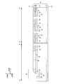
- FIG. 4 is a view showing a CC cross section in FIG.
- FIG. 4 is a view showing a cross section of the gate pad portion 105.
- the gate pad portion 105 includes an interlayer insulating film 52 as a second lower insulating film, a titanium film 42 as a second protective film, and a metal layer 44.
- the titanium film 42 is provided on the interlayer insulating film 52. Since the titanium film 42 occludes hydrogen, the active hydrogen can be prevented from entering the semiconductor substrate 10 not only in the active region 101 but also in the gate pad portion 105.
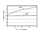
- FIG. 5 is a diagram showing the amount of change in the gate threshold (Vth) with respect to the gate bias application time.
- the gate bias was continuously applied to the gate electrode 34 to test and measure the change in the gate threshold.
- the horizontal axis represents the gate bias application time [hr]
- the vertical axis represents the gate threshold (Vth) change amount [V].
- “Comparative example” in FIG. 5 shows a test result when the titanium film 42 is provided only in the active region 101.
- “Example” in FIG. 5 shows a test result when the titanium film 42 is provided in the active region 101, the breakdown voltage structure portion 102, the gate runner portion 103, and the gate pad portion 105.
- the gate threshold change amount after 400 hours is 10 times or more larger in the comparative example than in the example.
- the test results in FIG. 5 indicate that it is effective to provide the titanium film 42 in addition to the active region 101 in order to suppress the gate threshold change amount.
- FIG. 6A to FIG. 6F are diagrams showing a manufacturing process of the semiconductor device 100. 6A to 6F, the CC section is omitted, but the layers, regions, films, and the like indicated by the same reference numerals in the AA section, the BB section, and the CC section are the same process. Created with. For example, the source region 26 and the contact region 28 in the active region 101, the breakdown voltage structure portion 102, and the gate pad portion 105 are formed in the process of FIG. 6B.
- FIG. 6A is a diagram illustrating a process of forming the drift layer 12 and a plurality of p-type regions.
- a first conductivity type layer 11 having an n-type impurity concentration of about 2.0E19 cm ⁇ 3 is prepared.
- E means 10 tiles.
- E19 means 10 to the 19th power.
- the first conductivity type layer 11 of this example is an n + type SiC substrate.
- the n + -type SiC substrate may have a (000-1) plane whose main surface has an off angle of about 4 degrees in the ⁇ 11-20> direction.
- a drift layer 12 having an n-type impurity concentration of about 1.0E16 cm ⁇ 3 is grown about 10 ⁇ m above the first conductivity type layer 11 by an epitaxial method.
- the n-type impurity in the first conductivity type layer 11 and the drift layer 12 is N (nitrogen), but other impurities may be used as long as they are n-type impurities.
- a well region 22 and a base region 24 having a p-type impurity concentration of about 2.0E16 cm ⁇ 3 are grown on the front surface side of the drift layer 12 by about 0.5 ⁇ m by an epitaxial method.
- the p-type impurity in this example is Al, but other impurities may be used as long as they are p-type impurities.
- the drift layer 12 is grown by about 0.5 ⁇ m by an epitaxial method.
- the second conductivity type region 39 is formed by forming the JTE high concentration region 37 and the JTE low concentration region 38 by an epitaxial method.
- the JTE high concentration region 37 can be made p-type and the JTE low concentration region 38 can be made p ⁇ type.
- FIG. 6B is a diagram illustrating a process of forming the source region 26 and the contact region 28.
- FIG. 6B is a diagram showing a step subsequent to FIG. 6A. 6B, the contact region 28 is selectively formed on the front surface side of the base region 24 by photolithography and ion implantation. Next, the source region 26 is selectively formed on the front surface side of the base region 24 by photolithography and ion implantation. Next, the semiconductor substrate 10 is heat-treated in order to activate the implanted impurities.
- FIG. 6C is a diagram illustrating a process of forming the insulating film 51.
- FIG. 6C is a diagram showing a step subsequent to FIG. 6B.
- an insulating film 51 is selectively provided on the semiconductor substrate 10.
- the insulating film 51 may be provided to have a thickness of 2,000 mm or more.
- FIG. 6D is a diagram showing a stage in which the gate insulating film 32, the gate electrode 34, the interlayer insulating film 36, and the interlayer insulating film 52 are formed.
- FIG. 6D is a diagram showing a step subsequent to FIG. 6C.
- the semiconductor substrate 10 is exposed to a temperature of about 1,000 ° C. in a mixed atmosphere of oxygen and hydrogen and thermally oxidized, thereby forming the gate insulating film 32.
- the thickness of the gate insulating film 32 may be about 100 nm.
- polycrystalline silicon doped with phosphorus is formed on the front surface side of the gate insulating film 32.
- the gate electrode 34 having polycrystalline silicon is formed by selectively removing the polycrystalline silicon by photolithography.
- the interlayer insulating film 36 is formed on the front surface side and the side surface of the gate electrode 34, and the interlayer insulating film 52 is formed so as to cover the entire upper portion of the semiconductor substrate 10 including the stepped portion 45 of the breakdown voltage structure portion 102. To do.
- the interlayer insulating film 36 and the interlayer insulating film 52 are PSG and have a thickness of about 1.0 ⁇ m.
- the gate insulating film 32, the interlayer insulating film 36, and the interlayer insulating film 52 are patterned by photolithography to form a plurality of contact portions 30.
- the semiconductor substrate 10 is heat-treated to reflow and planarize the interlayer insulating film 36 and the interlayer insulating film 52.
- FIG. 6E is a diagram showing a stage in which the titanium film 42 and the metal layer 44 are formed.
- FIG. 6E is a diagram showing a step subsequent to FIG. 6D.
- the titanium film 42 is patterned by photolithography.
- nickel (Ni) may be introduced into the semiconductor substrate 10 exposed at the contact portion 30 to form the nickel silicide region 29.
- the titanium film 42 in contact with the nickel silicide region 29 may have a titanium carbide region 43.
- the thickness of the titanium film 42 as the first protective film in the breakdown voltage structure 102 may be larger than the thickness of the titanium film 42 as the third protective film in the active region 101.
- the thickness of the titanium film 42 of the breakdown voltage structure 102 is set to be larger than 0.5 ⁇ m.
- the area of the titanium film 42 of the pressure-resistant structure 102 is about 10% of the whole.
- the thickness of the titanium film 42 as the third protective film in the active region 101 may be larger than the thickness of the titanium film 42 as the first protective film in the breakdown voltage structure 102.
- the thickness of the titanium film 42 in the active region 101 is set to be four times the thickness of the titanium film 42 in the breakdown voltage structure 102.
- a thickness of about 50 nm of the titanium film 42 may become a titanium aluminum alloy (TiAl). Titanium aluminum alloy has a smaller hydrogen storage effect than titanium. Therefore, by making the thickness of the titanium film 42 in the active region 101 thicker than that of the titanium film 42 in the pressure-resistant structure portion 102, the hydrogen storage effect in the active region 101 can be further ensured.
- the metal layer 44 is formed to a thickness of 5 ⁇ m.
- the metal layer 44 in this example is aluminum silicide (AlSi).
- AlSi aluminum silicide
- the metal layer 44 is selectively formed except for the step portion 45 of the pressure-resistant structure portion 102.
- FIG. 6F is a diagram showing a stage in which the passivation film 54 and the drain electrode 62 are formed.
- FIG. 6F is a view showing a step subsequent to FIG. 6E.
- nickel (Ni) is formed on the back surface side of the semiconductor substrate 10 by a sputtering method and heat-treated at 970 ° C.
- an ohmic junction region is formed on the back surface 16.
- Titanium (Ti), nickel (Ni), and gold (Au) are formed in this order on the back side of the ohmic junction region by sputtering.
- the drain electrode 62 is formed.
- a passivation film 54 is formed on the entire front surface side of the semiconductor substrate 10. Thereafter, the passivation film 54 is removed in a part of the active region 101 where the source terminal wiring is provided and a part of the gate pad portion 105 where the gate terminal wiring is provided. Thereby, the semiconductor device 100 is completed.
Landscapes
- Electrodes Of Semiconductors (AREA)
- Internal Circuitry In Semiconductor Integrated Circuit Devices (AREA)
Abstract
半導体装置に水素が侵入するとゲート構造のゲート電圧閾値(Vth)がシフトする。半導体装置の端部に位置する耐圧構造部から半導体装置へ水素が侵入することを防止する。活性領域と、活性領域の周りに設けられた耐圧構造部とが設けられる半導体基板と、半導体基板上において、耐圧構造部に設けられた第1の下部絶縁膜と、第1の下部絶縁膜上に設けられ、半導体基板と電気的に絶縁された、水素を吸蔵する第1の保護膜とを備える、半導体装置を提供する。
Description
本発明は、半導体装置に関する。
従来、ソース電極中のアルミニウム(Al)に起因する、層間絶縁膜の腐食、および、ポリシリコンで形成されたゲート電極とソース電極との短絡を防止するべく、バリアメタル層を設けていた。また、電気的コンタクトを改善するべく、Alを有するアノード電極およびカソード電極とポリシリコン層との間に、バリアメタル層を設けていた(例えば、特許文献1参照)。
[先行技術文献]
[特許文献]
[特許文献1] 特開2012-129503号公報
[非特許文献]
[非特許文献1] ケイ・シェナイ(K.Shenai)、外2名、オプティマム セミコンダクターズ フォー ハイパワー エレクトロニクス(Optimum Semiconductors for High-Power Electronics)、アイ・トリプル・イー トランザクションズ オン エレクトロン デバイシズ(IEEE Transactions on Electron Devices)、1989年9月、第36巻、第9号、p.1811-1823
[非特許文献2] ビー・ジャヤン・バリガ(B.Jayant Baliga)著、シリコンカーバイド パワー デバイシズ(Silicon Carbide Power Devices)、(米国)、ワールド サイエンティフィック パブリッシング カンパニー(World Scientific Publishing Co.)、2006年3月30日、p.61
[先行技術文献]
[特許文献]
[特許文献1] 特開2012-129503号公報
[非特許文献]
[非特許文献1] ケイ・シェナイ(K.Shenai)、外2名、オプティマム セミコンダクターズ フォー ハイパワー エレクトロニクス(Optimum Semiconductors for High-Power Electronics)、アイ・トリプル・イー トランザクションズ オン エレクトロン デバイシズ(IEEE Transactions on Electron Devices)、1989年9月、第36巻、第9号、p.1811-1823
[非特許文献2] ビー・ジャヤン・バリガ(B.Jayant Baliga)著、シリコンカーバイド パワー デバイシズ(Silicon Carbide Power Devices)、(米国)、ワールド サイエンティフィック パブリッシング カンパニー(World Scientific Publishing Co.)、2006年3月30日、p.61
半導体装置のおもて面に水分が付着した場合、水分に由来する水素が半導体装置の内部に入り込む場合がある。また、ソース電極としてアルミニウムを用いる場合に、アルミニウム中に含まれる水素が半導体装置内に入り込む場合がある。水素は還元作用を有するので、水素により半導体装置内の酸素が引き抜かれて、ゲート絶縁膜として用いられる二酸化シリコン等の絶縁膜の性質が変化する場合がある。これによりゲート構造のゲート電圧閾値(Vth)がシフトする。水素の半導体装置への侵入は、半導体装置の端部に位置する耐圧構造部においても問題となる。
本発明の第1の態様においては、半導体基板と第1の下部絶縁膜と第1の保護膜とを備える半導体装置を提供する。半導体基板は、活性領域と、耐圧構造部とを有してよい。耐圧構造部は、活性領域の周りに設けられてよい。第1の下部絶縁膜は、半導体基板上において、耐圧構造部に設けられてよい。第1の保護膜は、第1の下部絶縁膜上に設けられてよい。第1の保護膜は、半導体基板と電気的に絶縁されてよい。第1の保護膜は、水素を吸蔵してよい。
半導体基板は、第1導電型であってよい。半導体基板は、耐圧構造部のおもて面に第2導電型の領域を有してよい。第1の保護膜は、第2導電型の領域の上方を少なくとも覆ってよい。
第2導電型の領域は、活性領域から耐圧構造部に向かう方向において濃度が低くなる領域を有してよい。
耐圧構造部に設けられた第1の保護膜は、活性領域から電気的に分離されていてよい。
半導体装置は、耐圧構造部に設けられた第1の保護膜上に、第1の上部絶縁膜をさらに備えてよい。
第1の保護膜は、耐圧構造部において一体に形成されていてよい。
半導体基板は、耐圧構造部において、傾斜部および平坦部を有する段差部をさらに備えてよい。第1の保護膜は、耐圧構造部において、段差部を含む半導体基板の上方全体を覆って設けられていてよい。
半導体装置は、ゲートランナー部とゲートパッド部とをさらに備えてよい。ゲートランナー部は、活性領域と耐圧構造部との間に設けられてよい。ゲートパッド部は、活性領域とゲートランナー部との間に設けられてよい。ゲートランナー部およびゲートパッド部は、第2の下部絶縁膜と第2の保護膜とを有してよい。第2の下部絶縁膜は、半導体基板上に設けられてよい。第2の保護膜は、第2の下部絶縁膜上に設けられてよい。第2の保護膜は、水素を吸蔵してよい。
活性領域は、第3の下部絶縁膜と第3の保護膜とをさらに備えてよい。第3の下部絶縁膜は、半導体基板上に設けられてよい。第3の保護膜は、第3の下部絶縁膜上に設けられてよい。第3の保護膜は、水素を吸蔵してよい。
活性領域は、コンタクト部をさらに備えてよい。コンタクト部は、半導体基板と第3の保護膜との電気的接続を提供してよい。第3の保護膜は、半導体基板上に設けられてよい。コンタクト部において、半導体基板はニッケルシリサイドを少なくとも有してよい。コンタクト部において、第3の保護膜はチタンカーバイドを少なくとも有してよい。
耐圧構造部における第1の保護膜の厚さは、活性領域における第3の保護膜の厚さよりも大きくてよい。
活性領域における第3の保護膜の厚さは、耐圧構造部における第1の保護膜の厚さよりも大きくてよい。
なお、上記の発明の概要は、本発明の必要な特徴の全てを列挙したものではない。また、これらの特徴群のサブコンビネーションもまた、発明となりうる。
以下、発明の実施の形態を通じて本発明を説明するが、以下の実施形態は請求の範囲にかかる発明を限定するものではない。また、実施形態の中で説明されている特徴の組み合わせの全てが発明の解決手段に必須であるとは限らない。
本明細書において、nまたはpは、それぞれ電子または正孔が多数キャリアであることを意味する。また、nまたはpに付す+または-について、+はそれが記載されていないものよりも高不純物濃度であり、-はそれが記載されていないものよりも低不純物濃度であることを意味する。また、本明細書に記載した例では、第1導電型はn型を意味し第2導電型はp型を意味するが、他の例においては、第1導電型がp型を意味し第2導電型がn型を意味してもよい。
図1は、半導体装置100の平面図を示す図である。つまり、図1は、半導体基板10を上面視した場合を示す図である。半導体装置100は、x‐y平面に平行な面を有する。x方向とy方向とは互いに垂直な方向であり、z方向はx‐y平面に垂直な方向である。本明細書において、おもて面側とはx‐y平面に平行な面を有する物体の+z方向の側を意味し、裏面側とは当該物体の-z方向の側を意味するとする。物体のおもて面側と裏面側との間に位置する面は、当該物体の側面と称する。なお、半導体基板10のおもて面をおもて面14と記載し、半導体基板10の裏面を裏面16と記載する。
半導体装置100は、半導体基板10を有する。半導体基板10には、活性領域101および耐圧構造部102が設けられる。耐圧構造部102は、活性領域101の周りに設けられる。なお、半導体装置100においてaがbの周りに設けられるとは、半導体装置100を図1の上面視した場合に、aの周囲を囲んでbが設けられることを意味する。
本例の活性領域101は、縦型MOSFET(Metal Oxide Semiconductor Field Effect Transistor)を有する領域である。ただし、他の例においては、活性領域101は、縦型MOSFETに代えて、IGBT(Insulated Gate Bipolar Transisor)を有してもよい。
耐圧構造部102は、半導体基板10の端部における電界集中を緩和または分散させる機能を有する部分である。半導体基板10は、耐圧構造部102において、後述するJTE(Junction Termination Extension)構造を有する。JTE構造は、活性領域101の周りに設けられた後述のJTE高濃度領域37およびJTE低濃度領域38を有する。
半導体装置100は、ゲートランナー部103とゲートパッド部105とをさらに備える。ゲートランナー部103は、半導体装置100を上面視した場合に、活性領域101と耐圧構造部102との間に設けられる。ゲートランナー部103は、活性領域101の周りに設けられる。ゲートランナー部103は、後述のゲート電極34と電気的に接続された配線である。
ゲートパッド部105は、半導体装置100を上面視した場合に、活性領域101とゲートランナー部103との間に設けられる。ゲートパッド部105は、ゲートランナー部103に電気的に接続して設けられる。ゲートパッド部105は、ゲートランナー部103から活性領域101へ突出した部分である。ゲートパッド部105は、外部配線への電気的接続を提供する。例えば、ゲートパッド部105には、ゲート端子配線がワイヤボンディングにより接続される。
図2は、図1におけるA‐A断面を示す図である。図2は、活性領域101の断面を示す図である。本例の半導体基板10は、シリコンカーバイド(SiC)を有する。ただし、半導体基板10は、他のワイドギャップ半導体材料であってもよい。例えば他の例において、半導体基板10は、窒化ガリウム(GaN)を有する。
半導体基板10は、第1導電型である。半導体基板10は、裏面16側にn+型の第1導電型層11を有し、おもて面14側にn型のドリフト層12を有する。半導体基板10は、ドリフト層12のおもて面14側に、p型のウェル領域22、p型のベース領域24、n+型のソース領域26およびp+型のコンタクト領域28を有する。
ベース領域24の少なくとも一部は、ゲート電極34の下に設けられる。本明細書において、「上」または「上方」とは、半導体基板10の裏面16からおもて面14に向かう方向を指す。これに対して、「下」または「下方」とは、半導体基板10のおもて面14から裏面16に向かう方向を指す。ベース領域24は、チャネル形成領域として機能する。ゲート絶縁膜32を介してゲート電極34から電界が印加されると、ベース領域24の一部にチャネルが形成される。
n+型のソース領域26は、ベース領域24に挟まれてまたは囲まれて、ベース領域24中に設けられる。p+型のコンタクト領域28は、ソース領域26に挟まれてまたは囲まれて、ベース領域24中に設けられる。p+型のコンタクト領域28は、ソース電極との接触抵抗を下げる機能を有する。
ゲート絶縁膜32は、少なくともベース領域24とゲート電極34とを電気的に分離する。本例のゲート絶縁膜32は、おもて面14においてベース領域24とソース領域26に接して設けられる。
ゲート電極34は、ゲート絶縁膜32上に設けられる。第3の下部絶縁層としての層間絶縁膜36は、ゲート電極34上に位置する。層間絶縁膜36は、ゲート電極34のおもて面側および側面を囲んで設けられる。層間絶縁膜36は、PSG(Phosphosilicate Glass)膜またはBPSG(Borophosphosilicate Glass)膜であってよい。
層間絶縁膜36上には、第3の保護膜としてのチタン(Ti)膜42が設けられる。チタン膜42は、水素を吸蔵する機能を有する。チタン膜42は、チタンシリサイド(TiSix)を含んでもよい。
金属層44は、チタン膜42上に設けられる。金属層44は、アルミニウム(Al)であってよく、シリコン(Si)を重量比で1%含有するアルミニウムシリサイド(AlSi)等のアルミニウム合金であってもよい。チタン膜42および金属層44は、活性領域101においてソース電極として機能する。なお、半導体基板10の裏面16下にはドレイン電極62が設けられる。
コンタクト部30は、チタン膜42とソース領域26およびコンタクト領域28とが接触する領域である。コンタクト部30は、半導体基板10とチタン膜42との電気的接続を提供する。コンタクト部30において、ソース領域26の一部とコンタクト領域28とはニッケルシリサイド(NiSi)領域29を有する。また、コンタクト部30において、チタン膜42は、チタンカーバイド(TiC)領域43を少なくとも有する。
図3は、図1におけるB‐B断面を示す図である。図3は、活性領域101の端部、ゲートランナー部103および耐圧構造部102に渡る断面を示す図である。半導体基板10上において、絶縁膜51および層間絶縁膜52の積層体が、活性領域101の外周端部から耐圧構造部102の外周端部まで設けられる。絶縁膜51は、酸化シリコン(SiO2)等の酸化膜、PSGまたはBPSGであってよい。層間絶縁膜52は、層間絶縁膜36と同じ材料であってよい。層間絶縁膜52は、PSGまたはBPSGであってよい。
ゲートランナー部103は、第2の下部絶縁膜としての層間絶縁膜52と、第2の保護膜としてのチタン膜42と、金属層44とを有する。チタン膜42は、層間絶縁膜52上に設けられる。チタン膜42は、水素を吸蔵する。本例では、活性領域101に加えて、ゲートランナー部103においても活性水素が半導体基板10へ侵入することを防止できる。
耐圧構造部102は、少なくとも第1の下部絶縁膜としての層間絶縁膜52と、第1の保護膜としてのチタン膜42とを有する。なお、上述の記載から明らかなように、本例の第1~第3の保護膜はチタン膜42である。耐圧構造部102のチタン膜42は、層間絶縁膜52上に設けられているので、半導体基板10から電気的に絶縁されている。
本例では、水素を吸蔵するチタン膜42を耐圧構造部102にも設ける。これにより、活性水素が耐圧構造部102から半導体基板10に侵入することを防止できる。したがって、活性領域101のゲート閾値が変動することを防止できる。
耐圧構造部102のチタン膜42上に、第1の上部絶縁膜としてのパッシベーション膜54が設けられる。パッシベーション膜54は、活性領域101、耐圧構造部102およびゲートランナー部103において、最も上方に設けられる。なお、活性領域101およびゲートパッド部105では外部との電気的導通を確保するために、パッシベーション膜54が部分的に除去される。
耐圧構造部102のチタン膜42は、浮遊電位を有する。耐圧構造部102に設けられたチタン膜42は、活性領域101から電気的に分離されている。耐圧構造部102のチタン膜42は、同様に、ゲートランナー部103からも電気的に分離されている。耐圧構造部102とゲートランナー部103との間におけるチタン膜42の離間距離は、2μm以上10μm以下であってよい。なお、活性領域101とゲートランナー部103との間におけるチタン膜42の離間距離も、2μm以上10μm以下であってよい。
半導体基板10は、耐圧構造部102において、段差部45を有する。段差部45は、z方向の高さ位置の異なる2つの平坦部46と、2つの平坦部46の間の傾斜部47とを有する。2つの平坦部46のうち下方に位置する平坦部46には、第2導電型の領域39が設けられる。チタン膜42は浮遊電位を有するので、第2導電型の領域39には電圧が印加されない。それゆえ、耐圧構造部102は、フィールドプレート構造ではなくJTE構造として機能させることができる。これにより、絶縁膜51および層間絶縁膜52が絶縁破壊されることを防ぐことができる。
半導体基板10は、耐圧構造部102のおもて面14に第2導電型の領域39としてのJTE高濃度領域37およびJTE低濃度領域38を有する。JTE低濃度領域38は、JTE高濃度領域37よりも低いp型の不純物濃度を有する。本例のJTE高濃度領域37はp型不純物を有し、JTE低濃度領域38はp-型不純物を有する。つまり、第2導電型の領域39は、活性領域101から耐圧構造部102に向かう方向においてp型不純物の濃度が低くなる領域である。
チタン膜42は、耐圧構造部102において一体に形成されている。なお、チタン膜42が一体に形成されているとは、チタン膜42がベタ膜であることを意味する。例えば、耐圧構造部102におけるチタン膜42に穴および開口等は形成されていないことを意味する。
チタン膜42は、耐圧構造部102において第2導電型の領域39の上方を少なくとも覆う。本例のチタン膜42は、耐圧構造部102において、段差部45を含む半導体基板10の上方全体を覆って設けられている。すなわち、チタン膜42は耐圧構造部102の上方全体を覆って設けられてよい。これにより、水素がJTE高濃度領域37およびJTE低濃度領域38へ侵入することを防止できるので、耐圧構造部102における耐圧特性の変動を防止することができる。
図4は、図1におけるC‐C断面を示す図である。図4は、ゲートパッド部105の断面を示す図である。半導体基板10上において、絶縁膜51および層間絶縁膜52の積層体が、ゲートパッド部105から活性領域101まで設けられる。ゲートパッド部105は、第2の下部絶縁膜としての層間絶縁膜52と、第2の保護膜としてのチタン膜42と、金属層44とを有する。チタン膜42は、層間絶縁膜52上に設けられる。チタン膜42は、水素を吸蔵するので、活性領域101に加えて、ゲートパッド部105においても活性水素が半導体基板10へ侵入することを防止できる。
図5は、ゲートバイアス印加時間に対するゲート閾値(Vth)変化量を示す図である。ゲート電極34にゲートバイアスを連続して印加してゲート閾値の変化を試験して測定した。横軸は、ゲートバイアス印加時間[hr]であり、縦軸は、ゲート閾値(Vth)変化量[V]である。
図5中の「比較例」は、活性領域101のみにチタン膜42を設けた場合の試験結果を示す。これに対して、図5中の「実施例」は、活性領域101、耐圧構造部102、ゲートランナー部103およびゲートパッド部105にチタン膜42を設けた場合の試験結果を示す。図5から明らかであるように、例えば、400時間後のゲート閾値変化量は、比較例の方が実施例よりも10倍以上大きい。図5の試験結果は、活性領域101以外にもチタン膜42を設けることがゲート閾値変化量を抑えるためには有効であることを示している。
図6Aから図6Fは、半導体装置100の製造工程を示す図である。なお、図6Aから図6Fにおいては、C‐C断面を省略するが、A‐A断面、B‐B断面およびC‐C断面において同一の符号で示す層、領域および膜等は、同一の工程で作成される。例えば、活性領域101、耐圧構造部102およびゲートパッド部105におけるソース領域26およびコンタクト領域28は、図6Bの工程において形成される。
図6Aは、ドリフト層12および複数のp型領域を形成する工程を示す図である。まず、約2.0E19cm-3のn型不純物濃度を有する第1導電型層11を準備する。なお、Eは10の冪を意味する。例えばE19は、10の19乗を意味する。本例の第1導電型層11は、n+型SiC基板である。n+型SiC基板は、主面が<11-20>方向に4度程度のオフ角を有する(000-1)面であってよい。
次に、第1導電型層11の上方に、約1.0E16cm-3のn型不純物濃度を有するドリフト層12を、エピタキシャル法により約10μm成長させる。第1導電型層11およびドリフト層12におけるn型不純物はN(窒素)であるが、n型不純物であれば他の不純物を用いてもよい。
次に、ドリフト層12のおもて面側に、約2.0E16cm-3のp型不純物濃度を有するウェル領域22およびベース領域24を、エピタキシャル法により約0.5μm成長させる。本例のp型不純物はAlであるが、p型不純物であれば他の不純物を用いてもよい。なお、ウェル領域22およびベース領域24以外の領域は、ドリフト層12をエピタキシャル法により約0.5μm成長させる。
なお、ドリフト層12の端部付近を部分的にエッチングにより除去して、窪みを形成する。その後、エピタキシャル法によりJTE高濃度領域37およびJTE低濃度領域38を形成することにより、第2導電型の領域39を形成する。エピタキシャル成長時の不純物濃度を調整することにより、JTE高濃度領域37をp型とし、JTE低濃度領域38をp-型とすることができる。
図6Bは、ソース領域26およびコンタクト領域28を形成する工程を示す図である。図6Bは図6Aの後の工程を示す図である。図6Bの工程では、フォトリソグラフィーおよびイオン注入により、ベース領域24のおもて面側に、コンタクト領域28を選択的に形成する。次に、フォトリソグラフィーおよびイオン注入により、ベース領域24のおもて面側に、ソース領域26を選択的に形成する。次に、注入した不純物を活性化させるために半導体基板10を熱処理する。
図6Cは、絶縁膜51を形成する工程を示す図である。図6Cは図6Bの後の工程を示す図である。図6Cの工程では、半導体基板10上に選択的に絶縁膜51を設ける。絶縁膜51は、2,000Å以上の厚みを有するよう設けてよい。
図6Dは、ゲート絶縁膜32、ゲート電極34、層間絶縁膜36および層間絶縁膜52を形成する段階を示す図である。図6Dは図6Cの後の工程を示す図である。図6Dの工程では、酸素および水素の混合雰囲気下において半導体基板10を約1,000℃の温度に曝して熱酸化することにより、ゲート絶縁膜32を形成する。ゲート絶縁膜32の厚さは、約100nmであってよい。
次に、ゲート絶縁膜32のおもて面側に、リンがドープされた多結晶シリコンを形成する。次に、フォトリソグラフィーにより多結晶シリコンを選択に除去することにより、多結晶シリコンを有するゲート電極34を形成する。次に、ゲート電極34のおもて面側および側面に層間絶縁膜36を形成すると共に、耐圧構造部102の段差部45を含む半導体基板10の上方全体を覆うように層間絶縁膜52を形成する。層間絶縁膜36および層間絶縁膜52はPSGであり、膜厚を約1.0μmの厚さとする。
次に、ゲート絶縁膜32、層間絶縁膜36および層間絶縁膜52をフォトリソグラフィーによりパターニングして、複数のコンタクト部30を形成する。次に、半導体基板10を熱処理することにより、層間絶縁膜36および層間絶縁膜52をリフローさせて平坦化する。
図6Eは、チタン膜42および金属層44を形成する段階を示す図である。図6Eは図6Dの後の工程を示す図である。図6Eの工程では、チタン膜42をスパッタリングにより1,000Å(=100nm=0.1μm)以上0.5μm以下の厚みで形成する。0.1μm以上の厚みとすることで、段差部45におけるチタン膜42の段切れを防止することができる。
その後、チタン膜42をフォトリソグラフィーによりパターニングする。なお、チタン膜42を形成する前に、コンタクト部30に露出する半導体基板10にニッケル(Ni)を導入して、ニッケルシリサイド領域29を形成してよい。ニッケルシリサイド領域29と接するチタン膜42は、チタンカーバイド領域43を有してよい。
なお、変形例として、耐圧構造部102における第1の保護膜としてのチタン膜42の厚さは、活性領域101における第3の保護膜としてのチタン膜42の厚さよりも大きくてよい。例えば、耐圧構造部102のチタン膜42の厚さは、0.5μmよりも大きくする。半導体装置100を上面視した場合に、耐圧構造部102のチタン膜42の面積は、全体の10%程度である。耐圧構造部102のチタン膜42の厚みを大きくすることにより、耐圧構造部102における水素吸蔵効果をより確実にすることができる。
また、当該変形例に代えて、活性領域101における第3の保護膜としてのチタン膜42の厚さは、耐圧構造部102における第1の保護膜としてのチタン膜42の厚さよりも大きくてよい。例えば、活性領域101のチタン膜42の厚さを耐圧構造部102のチタン膜42の厚さの4倍とする。活性領域101ではアルミニウム(Al)を含む金属層44とチタン膜42とが反応することにより、チタン膜42の厚み50nm程度がチタンアルミ合金(TiAl)となる場合がある。チタンアルミ合金は、水素吸蔵効果がチタンに比べて小さい。そこで、活性領域101のチタン膜42の厚さを耐圧構造部102のチタン膜42よりも厚くすることで、活性領域101における水素吸蔵効果をより確実にすることができる。
次に、金属層44を5μmの厚さ形成する。本例の金属層44は、アルミニウムシリサイド(AlSi)である。金属層44は、耐圧構造部102の段差部45を除いて、選択的に形成する。
図6Fは、パッシベーション膜54およびドレイン電極62を形成する段階を示す図である。図6Fは図6Eの後の工程を示す図である。図6Fの工程では、まず、半導体基板10の裏面側に、スパッタ法によりニッケル(Ni)を成膜して、970℃で熱処理する。これにより、裏面16にオーミック接合領域を形成する。当該オーミック接合領域のさらに裏面側に、スパッタ法によりチタン(Ti)、ニッケル(Ni)および金(Au)をこの順に成膜する。これにより、ドレイン電極62を形成する。
次に、半導体基板10のおもて面側の全面にパッシベーション膜54を形成する。その後、ソース端子配線を設ける活性領域101の一部、および、ゲート端子配線を設けるゲートパッド部105の一部において、パッシベーション膜54を除去する。これにより、半導体装置100が完成する。
以上、本発明を実施の形態を用いて説明したが、本発明の技術的範囲は上記実施の形態に記載の範囲には限定されない。上記実施の形態に、多様な変更又は改良を加えることが可能であることが当業者に明らかである。その様な変更又は改良を加えた形態も本発明の技術的範囲に含まれ得ることが、請求の範囲の記載から明らかである。
請求の範囲、明細書、および図面中において示した装置、および方法における動作、手順、ステップ、および段階等の各処理の実行順序は、特段「より前に」、「先立って」等と明示しておらず、また、前の処理の結果を後の処理で用いるのでない限り、任意の順序で実現しうることに留意すべきである。請求の範囲、明細書、および図面中の動作フローに関して、便宜上「まず、」、「次に、」等を用いて説明したとしても、この順序で実施することが必須であることを意味するものではない。
10・・半導体基板、11・・第1導電型層、12・・ドリフト層、14・・おもて面、16・・裏面、22・・ウェル領域、24・・ベース領域、26・・ソース領域、28・・コンタクト領域、29・・ニッケルシリサイド領域、30・・コンタクト部、32・・ゲート絶縁膜、34・・ゲート電極、36・・層間絶縁膜、37・・JTE高濃度領域、38・・JTE低濃度領域、39・・第2導電型の領域、42・・チタン膜、43・・チタンカーバイド領域、44・・金属層、45・・段差部、46・・平坦部、47・・傾斜部、51・・絶縁膜、52・・層間絶縁膜、54・・パッシベーション膜、62・・ドレイン電極、100・・半導体装置、101・・活性領域、102・・耐圧構造部、103・・ゲートランナー部、105・・ゲートパッド部
Claims (12)
- 活性領域と、前記活性領域の周りに設けられた耐圧構造部とを有する半導体基板と、
前記半導体基板上において、前記耐圧構造部に設けられた第1の下部絶縁膜と、
前記第1の下部絶縁膜上に設けられ、前記半導体基板と電気的に絶縁された、水素を吸蔵する第1の保護膜と
を備える、半導体装置。 - 前記半導体基板は、第1導電型であり、
前記半導体基板は、前記耐圧構造部のおもて面に第2導電型の領域を有し、
前記第1の保護膜は、前記第2導電型の領域の上方を少なくとも覆う
請求項1に記載の半導体装置。 - 前記第2導電型の領域は、前記活性領域から前記耐圧構造部に向かう方向において濃度が低くなる領域を有する
請求項2に記載の半導体装置。 - 前記耐圧構造部に設けられた前記第1の保護膜は、前記活性領域から電気的に分離されている
請求項3に記載の半導体装置。 - 前記耐圧構造部に設けられた前記第1の保護膜上に、第1の上部絶縁膜をさらに備える
請求項4に記載の半導体装置。 - 前記第1の保護膜は、前記耐圧構造部において一体に形成されている
請求項4に記載の半導体装置。 - 前記半導体基板は、前記耐圧構造部において、傾斜部および平坦部を有する段差部をさらに備え、
前記第1の保護膜は、前記耐圧構造部において、前記段差部を含む前記半導体基板の上方全体を覆って設けられている
請求項6に記載の半導体装置。 - 前記活性領域と前記耐圧構造部との間におけるゲートランナー部と、
前記活性領域と前記ゲートランナー部との間におけるゲートパッド部と
をさらに備え、
前記ゲートランナー部および前記ゲートパッド部は、
前記半導体基板上における第2の下部絶縁膜と、
前記第2の下部絶縁膜上に設けられた、水素を吸蔵する第2の保護膜と
を有する
請求項1または2に記載の半導体装置。 - 前記活性領域は、
前記半導体基板上に設けられた第3の下部絶縁膜と、
前記第3の下部絶縁膜上に設けられた、水素を吸蔵する第3の保護膜と
をさらに備える、
請求項1または2に記載の半導体装置。 - 前記活性領域は、前記半導体基板と前記半導体基板上に設けられた前記第3の保護膜との電気的接続を提供するコンタクト部をさらに備え、
前記コンタクト部において、前記半導体基板はニッケルシリサイドを少なくとも有し、
前記コンタクト部において、前記第3の保護膜はチタンカーバイドを少なくとも有する
請求項9に記載の半導体装置。 - 前記耐圧構造部における前記第1の保護膜の厚さは、前記活性領域における前記第3の保護膜の厚さよりも大きい
請求項9に記載の半導体装置。 - 前記活性領域における前記第3の保護膜の厚さは、前記耐圧構造部における前記第1の保護膜の厚さよりも大きい
請求項9に記載の半導体装置。
Priority Applications (3)
| Application Number | Priority Date | Filing Date | Title |
|---|---|---|---|
| JP2017514055A JP6256659B2 (ja) | 2015-04-20 | 2016-04-06 | 半導体装置 |
| CN201680002943.5A CN106688104B (zh) | 2015-04-20 | 2016-04-06 | 半导体装置 |
| US15/475,144 US10090379B2 (en) | 2015-04-20 | 2017-03-31 | Hydrogen occlusion semiconductor device |
Applications Claiming Priority (4)
| Application Number | Priority Date | Filing Date | Title |
|---|---|---|---|
| JP2015085620 | 2015-04-20 | ||
| JP2015-085620 | 2015-04-20 | ||
| JP2015-122041 | 2015-06-17 | ||
| JP2015122041 | 2015-06-17 |
Related Child Applications (1)
| Application Number | Title | Priority Date | Filing Date |
|---|---|---|---|
| US15/475,144 Continuation US10090379B2 (en) | 2015-04-20 | 2017-03-31 | Hydrogen occlusion semiconductor device |
Publications (1)
| Publication Number | Publication Date |
|---|---|
| WO2016170978A1 true WO2016170978A1 (ja) | 2016-10-27 |
Family
ID=57143930
Family Applications (1)
| Application Number | Title | Priority Date | Filing Date |
|---|---|---|---|
| PCT/JP2016/061206 Ceased WO2016170978A1 (ja) | 2015-04-20 | 2016-04-06 | 半導体装置 |
Country Status (4)
| Country | Link |
|---|---|
| US (1) | US10090379B2 (ja) |
| JP (1) | JP6256659B2 (ja) |
| CN (1) | CN106688104B (ja) |
| WO (1) | WO2016170978A1 (ja) |
Cited By (3)
| Publication number | Priority date | Publication date | Assignee | Title |
|---|---|---|---|---|
| WO2018156374A1 (en) * | 2017-02-21 | 2018-08-30 | Raytheon Company | Nitride structure having gold-free contact and methods for forming such structures |
| US10096550B2 (en) | 2017-02-21 | 2018-10-09 | Raytheon Company | Nitride structure having gold-free contact and methods for forming such structures |
| JP2022543376A (ja) * | 2019-08-01 | 2022-10-12 | ヒタチ・エナジー・スウィツァーランド・アクチェンゲゼルシャフト | 炭化珪素トランジスタデバイス |
Families Citing this family (7)
| Publication number | Priority date | Publication date | Assignee | Title |
|---|---|---|---|---|
| JP6857488B2 (ja) * | 2016-11-29 | 2021-04-14 | 株式会社日立製作所 | 半導体装置の製造方法 |
| US11158703B2 (en) * | 2019-06-05 | 2021-10-26 | Microchip Technology Inc. | Space efficient high-voltage termination and process for fabricating same |
| JP7588083B2 (ja) * | 2019-09-30 | 2024-11-21 | ローム株式会社 | 半導体装置 |
| JP7401416B2 (ja) * | 2020-09-11 | 2023-12-19 | 株式会社東芝 | 半導体装置 |
| CN112786683B (zh) * | 2020-12-29 | 2022-07-15 | 浙江清华长三角研究院 | 一种功率器件 |
| IT202100003653A1 (it) * | 2021-02-17 | 2022-08-17 | St Microelectronics Srl | Dispositivo mosfet di carburo di silicio, a conduzione verticale, avente struttura di polarizzazione di porta perfezionata e relativo procedimento di fabbricazione |
| JP7803088B2 (ja) * | 2021-11-12 | 2026-01-21 | 富士電機株式会社 | 半導体装置および半導体装置の製造方法 |
Citations (4)
| Publication number | Priority date | Publication date | Assignee | Title |
|---|---|---|---|---|
| JPH0277128A (ja) * | 1988-09-13 | 1990-03-16 | Fujitsu Ltd | 半導体装置 |
| JPH07326744A (ja) * | 1994-05-31 | 1995-12-12 | Mitsubishi Electric Corp | 半導体装置及びその製造方法 |
| JP2013232564A (ja) * | 2012-04-27 | 2013-11-14 | National Institute Of Advanced Industrial & Technology | 半導体装置および半導体装置の製造方法 |
| US20140299887A1 (en) * | 2013-04-04 | 2014-10-09 | Monolith Semiconductor, Inc. | Semiconductor devices comprising getter layers and methods of making and using the same |
Family Cites Families (23)
| Publication number | Priority date | Publication date | Assignee | Title |
|---|---|---|---|---|
| JPH0397827A (ja) * | 1989-09-11 | 1991-04-23 | Agency Of Ind Science & Technol | チタン―クロム―銅系水素吸蔵合金 |
| TW286435B (ja) * | 1994-07-27 | 1996-09-21 | Siemens Ag | |
| US5951945A (en) * | 1995-06-13 | 1999-09-14 | Mitsubishi Materials Corporation | Hydrogen occluding alloy and electrode made of the alloy |
| JPH11354637A (ja) | 1998-06-11 | 1999-12-24 | Oki Electric Ind Co Ltd | 配線の接続構造及び配線の接続部の形成方法 |
| KR100386034B1 (ko) | 2000-12-06 | 2003-06-02 | 에이에스엠 마이크로케미스트리 리미티드 | 확산 방지막의 결정립계를 금속산화물로 충진한 구리 배선구조의 반도체 소자 제조 방법 |
| JP2002280523A (ja) | 2001-03-16 | 2002-09-27 | Nec Corp | 半導体記憶装置とその製造方法 |
| JP2003197773A (ja) | 2001-12-27 | 2003-07-11 | Toshiba Corp | 半導体装置及びその製造方法 |
| JP2005175357A (ja) | 2003-12-15 | 2005-06-30 | Nissan Motor Co Ltd | 半導体装置とその製造方法 |
| DE102007030755B3 (de) * | 2007-07-02 | 2009-02-19 | Infineon Technologies Austria Ag | Halbleiterbauelement mit einem einen Graben aufweisenden Randabschluss und Verfahren zur Herstellung eines Randabschlusses |
| JP2009194127A (ja) | 2008-02-14 | 2009-08-27 | Panasonic Corp | 半導体装置およびその製造方法 |
| JP5533104B2 (ja) | 2010-03-23 | 2014-06-25 | 日産自動車株式会社 | 半導体装置 |
| US8564072B2 (en) | 2010-04-02 | 2013-10-22 | Taiwan Semiconductor Manufacturing Company, Ltd. | Semiconductor device having a blocking structure and method of manufacturing the same |
| JP5694119B2 (ja) | 2010-11-25 | 2015-04-01 | 三菱電機株式会社 | 炭化珪素半導体装置 |
| JP2012186318A (ja) | 2011-03-05 | 2012-09-27 | Shindengen Electric Mfg Co Ltd | 高耐圧半導体装置 |
| JP5742668B2 (ja) | 2011-10-31 | 2015-07-01 | 三菱電機株式会社 | 炭化珪素半導体装置 |
| JP2013201357A (ja) | 2012-03-26 | 2013-10-03 | Mitsubishi Electric Corp | 炭化珪素半導体装置とその製造方法 |
| US9991399B2 (en) * | 2012-10-04 | 2018-06-05 | Cree, Inc. | Passivation structure for semiconductor devices |
| JP6048126B2 (ja) | 2012-12-25 | 2016-12-21 | 日産自動車株式会社 | 半導体装置及び半導体装置の製造方法 |
| US8994118B2 (en) * | 2013-04-04 | 2015-03-31 | Monolith Semiconductor, Inc. | Semiconductor devices comprising getter layers and methods of making and using the same |
| US9595469B2 (en) * | 2013-11-04 | 2017-03-14 | Infineon Technologies Ag | Semiconductor device and method for producing the same |
| US9570542B2 (en) * | 2014-04-01 | 2017-02-14 | Infineon Technologies Ag | Semiconductor device including a vertical edge termination structure and method of manufacturing |
| JP6387791B2 (ja) * | 2014-10-29 | 2018-09-12 | 富士電機株式会社 | 半導体装置の製造方法 |
| JP6380666B2 (ja) * | 2015-04-20 | 2018-08-29 | 富士電機株式会社 | 半導体装置 |
-
2016
- 2016-04-06 CN CN201680002943.5A patent/CN106688104B/zh active Active
- 2016-04-06 JP JP2017514055A patent/JP6256659B2/ja active Active
- 2016-04-06 WO PCT/JP2016/061206 patent/WO2016170978A1/ja not_active Ceased
-
2017
- 2017-03-31 US US15/475,144 patent/US10090379B2/en active Active
Patent Citations (4)
| Publication number | Priority date | Publication date | Assignee | Title |
|---|---|---|---|---|
| JPH0277128A (ja) * | 1988-09-13 | 1990-03-16 | Fujitsu Ltd | 半導体装置 |
| JPH07326744A (ja) * | 1994-05-31 | 1995-12-12 | Mitsubishi Electric Corp | 半導体装置及びその製造方法 |
| JP2013232564A (ja) * | 2012-04-27 | 2013-11-14 | National Institute Of Advanced Industrial & Technology | 半導体装置および半導体装置の製造方法 |
| US20140299887A1 (en) * | 2013-04-04 | 2014-10-09 | Monolith Semiconductor, Inc. | Semiconductor devices comprising getter layers and methods of making and using the same |
Cited By (8)
| Publication number | Priority date | Publication date | Assignee | Title |
|---|---|---|---|---|
| WO2018156374A1 (en) * | 2017-02-21 | 2018-08-30 | Raytheon Company | Nitride structure having gold-free contact and methods for forming such structures |
| US10096550B2 (en) | 2017-02-21 | 2018-10-09 | Raytheon Company | Nitride structure having gold-free contact and methods for forming such structures |
| US10224285B2 (en) | 2017-02-21 | 2019-03-05 | Raytheon Company | Nitride structure having gold-free contact and methods for forming such structures |
| CN110192283A (zh) * | 2017-02-21 | 2019-08-30 | 雷声公司 | 具有无金接触部的氮化物结构及形成这种结构的方法 |
| AU2018224009B2 (en) * | 2017-02-21 | 2022-06-09 | Raytheon Company | Nitride structure having gold-free contact and methods for forming such structures |
| JP2022543376A (ja) * | 2019-08-01 | 2022-10-12 | ヒタチ・エナジー・スウィツァーランド・アクチェンゲゼルシャフト | 炭化珪素トランジスタデバイス |
| JP7486571B2 (ja) | 2019-08-01 | 2024-05-17 | ヒタチ・エナジー・リミテッド | 炭化珪素トランジスタデバイス |
| US12062698B2 (en) | 2019-08-01 | 2024-08-13 | Hitachi Energy Ltd | Silicon carbide transistor device |
Also Published As
| Publication number | Publication date |
|---|---|
| US10090379B2 (en) | 2018-10-02 |
| CN106688104B (zh) | 2020-03-17 |
| US20170207301A1 (en) | 2017-07-20 |
| JP6256659B2 (ja) | 2018-01-10 |
| JPWO2016170978A1 (ja) | 2017-08-03 |
| CN106688104A (zh) | 2017-05-17 |
Similar Documents
| Publication | Publication Date | Title |
|---|---|---|
| JP6256659B2 (ja) | 半導体装置 | |
| US9472403B2 (en) | Power semiconductor switch with plurality of trenches | |
| US9419133B2 (en) | Semiconductor device and fabrication method of semiconductor device | |
| JP6911486B2 (ja) | 炭化珪素半導体装置および炭化珪素半導体装置の製造方法 | |
| JP7087280B2 (ja) | 炭化珪素半導体装置および炭化珪素半導体装置の製造方法 | |
| CN106796955B (zh) | 半导体装置 | |
| JP6561759B2 (ja) | 半導体装置および半導体装置の製造方法 | |
| US9972572B2 (en) | Semiconductor device having a barrier layer | |
| JPWO2016104264A1 (ja) | 半導体装置 | |
| US10079298B2 (en) | Semiconductor device and method of manufacturing semiconductor device | |
| JP2017092355A (ja) | 半導体装置および半導体装置の製造方法 | |
| US10141439B2 (en) | Semiconductor device and method of manufacturing the same | |
| CN107408577A (zh) | 半导体装置及半导体装置的制造方法 | |
| WO2016013472A1 (ja) | 半導体装置および半導体装置の製造方法 | |
| US10269952B2 (en) | Semiconductor device having steps in a termination region and manufacturing method thereof | |
| JP2017152732A (ja) | 半導体装置および半導体装置の製造方法 | |
| JP6589263B2 (ja) | 半導体装置 | |
| US10559514B2 (en) | Semiconductor device | |
| JP2017092364A (ja) | 半導体装置および半導体装置の製造方法 | |
| JP6737379B2 (ja) | 半導体装置 | |
| JP2008226997A (ja) | 半導体装置およびその製造方法 | |
| JP7113985B2 (ja) | 半導体素子及び半導体素子の製造方法 | |
| JP6350760B2 (ja) | 半導体装置および半導体装置の製造方法 | |
| JP6265278B2 (ja) | 炭化珪素半導体装置およびその製造方法 |
Legal Events
| Date | Code | Title | Description |
|---|---|---|---|
| 121 | Ep: the epo has been informed by wipo that ep was designated in this application |
Ref document number: 16782999 Country of ref document: EP Kind code of ref document: A1 |
|
| ENP | Entry into the national phase |
Ref document number: 2017514055 Country of ref document: JP Kind code of ref document: A |
|
| NENP | Non-entry into the national phase |
Ref country code: DE |
|
| 122 | Ep: pct application non-entry in european phase |
Ref document number: 16782999 Country of ref document: EP Kind code of ref document: A1 |