WO2016158226A1 - 太陽電池及びその製造方法 - Google Patents
太陽電池及びその製造方法 Download PDFInfo
- Publication number
- WO2016158226A1 WO2016158226A1 PCT/JP2016/057042 JP2016057042W WO2016158226A1 WO 2016158226 A1 WO2016158226 A1 WO 2016158226A1 JP 2016057042 W JP2016057042 W JP 2016057042W WO 2016158226 A1 WO2016158226 A1 WO 2016158226A1
- Authority
- WO
- WIPO (PCT)
- Prior art keywords
- layer
- type semiconductor
- semiconductor layer
- protective layer
- silicon
- Prior art date
- Legal status (The legal status is an assumption and is not a legal conclusion. Google has not performed a legal analysis and makes no representation as to the accuracy of the status listed.)
- Ceased
Links
Images

Classifications
-
- H—ELECTRICITY
- H10—SEMICONDUCTOR DEVICES; ELECTRIC SOLID-STATE DEVICES NOT OTHERWISE PROVIDED FOR
- H10F—INORGANIC SEMICONDUCTOR DEVICES SENSITIVE TO INFRARED RADIATION, LIGHT, ELECTROMAGNETIC RADIATION OF SHORTER WAVELENGTH OR CORPUSCULAR RADIATION
- H10F10/00—Individual photovoltaic cells, e.g. solar cells
- H10F10/10—Individual photovoltaic cells, e.g. solar cells having potential barriers
- H10F10/14—Photovoltaic cells having only PN homojunction potential barriers
- H10F10/146—Back-junction photovoltaic cells, e.g. having interdigitated base-emitter regions on the back side
-
- H—ELECTRICITY
- H10—SEMICONDUCTOR DEVICES; ELECTRIC SOLID-STATE DEVICES NOT OTHERWISE PROVIDED FOR
- H10F—INORGANIC SEMICONDUCTOR DEVICES SENSITIVE TO INFRARED RADIATION, LIGHT, ELECTROMAGNETIC RADIATION OF SHORTER WAVELENGTH OR CORPUSCULAR RADIATION
- H10F10/00—Individual photovoltaic cells, e.g. solar cells
- H10F10/10—Individual photovoltaic cells, e.g. solar cells having potential barriers
- H10F10/16—Photovoltaic cells having only PN heterojunction potential barriers
- H10F10/164—Photovoltaic cells having only PN heterojunction potential barriers comprising heterojunctions with Group IV materials, e.g. ITO/Si or GaAs/SiGe photovoltaic cells
- H10F10/165—Photovoltaic cells having only PN heterojunction potential barriers comprising heterojunctions with Group IV materials, e.g. ITO/Si or GaAs/SiGe photovoltaic cells the heterojunctions being Group IV-IV heterojunctions, e.g. Si/Ge, SiGe/Si or Si/SiC photovoltaic cells
- H10F10/166—Photovoltaic cells having only PN heterojunction potential barriers comprising heterojunctions with Group IV materials, e.g. ITO/Si or GaAs/SiGe photovoltaic cells the heterojunctions being Group IV-IV heterojunctions, e.g. Si/Ge, SiGe/Si or Si/SiC photovoltaic cells the Group IV-IV heterojunctions being heterojunctions of crystalline and amorphous materials, e.g. silicon heterojunction [SHJ] photovoltaic cells
-
- H—ELECTRICITY
- H10—SEMICONDUCTOR DEVICES; ELECTRIC SOLID-STATE DEVICES NOT OTHERWISE PROVIDED FOR
- H10F—INORGANIC SEMICONDUCTOR DEVICES SENSITIVE TO INFRARED RADIATION, LIGHT, ELECTROMAGNETIC RADIATION OF SHORTER WAVELENGTH OR CORPUSCULAR RADIATION
- H10F71/00—Manufacture or treatment of devices covered by this subclass
- H10F71/10—Manufacture or treatment of devices covered by this subclass the devices comprising amorphous semiconductor material
-
- H—ELECTRICITY
- H10—SEMICONDUCTOR DEVICES; ELECTRIC SOLID-STATE DEVICES NOT OTHERWISE PROVIDED FOR
- H10F—INORGANIC SEMICONDUCTOR DEVICES SENSITIVE TO INFRARED RADIATION, LIGHT, ELECTROMAGNETIC RADIATION OF SHORTER WAVELENGTH OR CORPUSCULAR RADIATION
- H10F71/00—Manufacture or treatment of devices covered by this subclass
- H10F71/10—Manufacture or treatment of devices covered by this subclass the devices comprising amorphous semiconductor material
- H10F71/103—Manufacture or treatment of devices covered by this subclass the devices comprising amorphous semiconductor material including only Group IV materials
-
- H—ELECTRICITY
- H10—SEMICONDUCTOR DEVICES; ELECTRIC SOLID-STATE DEVICES NOT OTHERWISE PROVIDED FOR
- H10F—INORGANIC SEMICONDUCTOR DEVICES SENSITIVE TO INFRARED RADIATION, LIGHT, ELECTROMAGNETIC RADIATION OF SHORTER WAVELENGTH OR CORPUSCULAR RADIATION
- H10F71/00—Manufacture or treatment of devices covered by this subclass
- H10F71/121—The active layers comprising only Group IV materials
-
- H—ELECTRICITY
- H10—SEMICONDUCTOR DEVICES; ELECTRIC SOLID-STATE DEVICES NOT OTHERWISE PROVIDED FOR
- H10F—INORGANIC SEMICONDUCTOR DEVICES SENSITIVE TO INFRARED RADIATION, LIGHT, ELECTROMAGNETIC RADIATION OF SHORTER WAVELENGTH OR CORPUSCULAR RADIATION
- H10F71/00—Manufacture or treatment of devices covered by this subclass
- H10F71/139—Manufacture or treatment of devices covered by this subclass using temporary substrates
- H10F71/1395—Manufacture or treatment of devices covered by this subclass using temporary substrates for thin-film devices
-
- H—ELECTRICITY
- H10—SEMICONDUCTOR DEVICES; ELECTRIC SOLID-STATE DEVICES NOT OTHERWISE PROVIDED FOR
- H10F—INORGANIC SEMICONDUCTOR DEVICES SENSITIVE TO INFRARED RADIATION, LIGHT, ELECTROMAGNETIC RADIATION OF SHORTER WAVELENGTH OR CORPUSCULAR RADIATION
- H10F77/00—Constructional details of devices covered by this subclass
- H10F77/10—Semiconductor bodies
- H10F77/14—Shape of semiconductor bodies; Shapes, relative sizes or dispositions of semiconductor regions within semiconductor bodies
-
- H—ELECTRICITY
- H10—SEMICONDUCTOR DEVICES; ELECTRIC SOLID-STATE DEVICES NOT OTHERWISE PROVIDED FOR
- H10F—INORGANIC SEMICONDUCTOR DEVICES SENSITIVE TO INFRARED RADIATION, LIGHT, ELECTROMAGNETIC RADIATION OF SHORTER WAVELENGTH OR CORPUSCULAR RADIATION
- H10F77/00—Constructional details of devices covered by this subclass
- H10F77/10—Semiconductor bodies
- H10F77/14—Shape of semiconductor bodies; Shapes, relative sizes or dispositions of semiconductor regions within semiconductor bodies
- H10F77/148—Shapes of potential barriers
-
- H—ELECTRICITY
- H10—SEMICONDUCTOR DEVICES; ELECTRIC SOLID-STATE DEVICES NOT OTHERWISE PROVIDED FOR
- H10F—INORGANIC SEMICONDUCTOR DEVICES SENSITIVE TO INFRARED RADIATION, LIGHT, ELECTROMAGNETIC RADIATION OF SHORTER WAVELENGTH OR CORPUSCULAR RADIATION
- H10F77/00—Constructional details of devices covered by this subclass
- H10F77/20—Electrodes
- H10F77/206—Electrodes for devices having potential barriers
- H10F77/211—Electrodes for devices having potential barriers for photovoltaic cells
- H10F77/219—Arrangements for electrodes of back-contact photovoltaic cells
-
- H—ELECTRICITY
- H10—SEMICONDUCTOR DEVICES; ELECTRIC SOLID-STATE DEVICES NOT OTHERWISE PROVIDED FOR
- H10F—INORGANIC SEMICONDUCTOR DEVICES SENSITIVE TO INFRARED RADIATION, LIGHT, ELECTROMAGNETIC RADIATION OF SHORTER WAVELENGTH OR CORPUSCULAR RADIATION
- H10F77/00—Constructional details of devices covered by this subclass
- H10F77/30—Coatings
- H10F77/306—Coatings for devices having potential barriers
- H10F77/311—Coatings for devices having potential barriers for photovoltaic cells
-
- Y—GENERAL TAGGING OF NEW TECHNOLOGICAL DEVELOPMENTS; GENERAL TAGGING OF CROSS-SECTIONAL TECHNOLOGIES SPANNING OVER SEVERAL SECTIONS OF THE IPC; TECHNICAL SUBJECTS COVERED BY FORMER USPC CROSS-REFERENCE ART COLLECTIONS [XRACs] AND DIGESTS
- Y02—TECHNOLOGIES OR APPLICATIONS FOR MITIGATION OR ADAPTATION AGAINST CLIMATE CHANGE
- Y02E—REDUCTION OF GREENHOUSE GAS [GHG] EMISSIONS, RELATED TO ENERGY GENERATION, TRANSMISSION OR DISTRIBUTION
- Y02E10/00—Energy generation through renewable energy sources
- Y02E10/50—Photovoltaic [PV] energy
- Y02E10/547—Monocrystalline silicon PV cells
-
- Y—GENERAL TAGGING OF NEW TECHNOLOGICAL DEVELOPMENTS; GENERAL TAGGING OF CROSS-SECTIONAL TECHNOLOGIES SPANNING OVER SEVERAL SECTIONS OF THE IPC; TECHNICAL SUBJECTS COVERED BY FORMER USPC CROSS-REFERENCE ART COLLECTIONS [XRACs] AND DIGESTS
- Y02—TECHNOLOGIES OR APPLICATIONS FOR MITIGATION OR ADAPTATION AGAINST CLIMATE CHANGE
- Y02P—CLIMATE CHANGE MITIGATION TECHNOLOGIES IN THE PRODUCTION OR PROCESSING OF GOODS
- Y02P70/00—Climate change mitigation technologies in the production process for final industrial or consumer products
- Y02P70/50—Manufacturing or production processes characterised by the final manufactured product
Definitions
- the present invention relates to a solar cell and a manufacturing method thereof.
- a general crystalline silicon-based solar cell is a double-sided electrode type, and includes a p-type semiconductor layer on one surface of a crystalline silicon substrate and an n-type semiconductor layer on the other surface, and either the p-layer side or the n-layer side. Is the light receiving surface. Metal electrodes are provided on the light receiving surface and the back surface in order to extract current efficiently. When sunlight is taken in from the light receiving surface, electron-hole pairs are generated in the crystalline silicon substrate, and current is taken out through electrodes provided on the p layer and the n layer, respectively. In a double-sided electrode type solar cell, the shielding of sunlight by the metal electrode on the light receiving surface side (shadowing loss) is a cause of lowering the conversion efficiency.
- a back electrode solar cell in which both a p-type semiconductor layer and an n-type semiconductor layer are provided on the back side of a crystalline silicon substrate, and electrodes are formed thereon. Development is underway. In the back contact solar cell, since it is not necessary to form an electrode on the light receiving surface side, the sunlight receiving efficiency can be increased and the conversion efficiency can be improved.
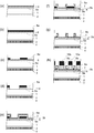
- FIG. 4 is a process conceptual diagram of a back contact solar cell manufacturing method disclosed in Patent Document 1.
- the intrinsic semiconductor layer 2 is formed on the light receiving surface side of the crystalline silicon substrate 1, and the intrinsic semiconductor layer 5a and the first conductivity type semiconductor layer 6 are formed in this order on the back surface side.
- the light receiving surface side protective layer 4 is formed on the intrinsic semiconductor layer 2 on the light receiving surface side, and the insulating layer 8a is formed on the first conductivity type semiconductor layer 6 on the back surface side. Is done.
- a part of the insulating layer 8a on the back surface side is removed by etching.
- the first conductive type semiconductor layer 6 and the intrinsic semiconductor are formed.
- a part of the layer 5a is removed by etching, and the crystalline silicon substrate 1 is exposed.
- the intrinsic semiconductor layer 5b and the second conductive semiconductor layer 7 are formed on substantially the entire back surface including the first conductive semiconductor layer 6 and the insulating layer 8a.
- FIG. 4 (f) after the second semiconductor layer 7 and the intrinsic semiconductor layer 5b on the insulating layer 8a are partially removed by etching, as shown in FIG. Using the layer 7 as a mask, the insulating layer 8a is etched to expose the first conductivity type semiconductor layer 6.
- patterned semiconductor layers p layer and n layer
- electrodes are formed on the first conductive semiconductor layer 6 and the second conductive semiconductor layer 7, thereby completing the back contact solar cell.
- the insulating layer 8a is made of a silicon alloy such as silicon oxide, silicon nitride, or silicon oxynitride, and is removed by etching using an acid-based etchant (etching agent) such as a hydrofluoric acid (HF) aqueous solution.
- etching agent such as a hydrofluoric acid (HF) aqueous solution.
- the first conductive semiconductor layer 6 and the second conductive semiconductor layer 7 are made of, for example, conductive silicon.
- the second conductive type semiconductor layer 7 is used as an etching mask, and the etching is terminated when the first conductive type semiconductor layer 6 is exposed.
- the formation of a mask layer for pattern etching can be omitted.
- an object of the present invention is to provide a back contact type solar cell in which deterioration in characteristics due to patterning is suppressed.
- the etchant at the time of patterning the insulating layer is in contact with the p-type semiconductor layer and causes damage, which is a cause of deterioration in characteristics.
- an intrinsic silicon-based layer and / or an n-type silicon-based layer as a base layer between the p-type semiconductor layer and the insulating layer, contact between the etchant used for etching the insulating layer and the p-type semiconductor layer is prevented. it can. Therefore, a back contact type crystalline silicon solar cell with improved contact resistance and open circuit voltage can be obtained.
- the present invention relates to a solar cell including an n-type semiconductor layer and a p-type semiconductor layer on a first main surface of a crystalline silicon substrate, and a manufacturing method thereof.
- the n-type semiconductor layer includes a part of the p-type semiconductor layer forming region provided with the p-type semiconductor layer and a p-type semiconductor layer provided with no p-type semiconductor layer. It is provided so as to straddle the non-forming region.
- protection is provided between the p-type semiconductor layer and the n-type semiconductor layer.
- a layer is provided.
- the protective layer preferably has a base layer having at least one of an intrinsic silicon-based layer and an n-type silicon-based layer and an insulating layer in this order from the p-type semiconductor layer side.
- the underlying layer (underlying protective layer) in the protective layer is preferably an intrinsic silicon-based layer.
- the insulating layer in the protective layer is preferably at least one selected from silicon oxide, silicon nitride, and silicon oxynitride.
- the p-type semiconductor layer is preferably a p-type silicon-based layer.
- a p-type semiconductor layer forming region in which a p-type semiconductor layer and a protective layer are provided in this order, and a p-type semiconductor layer and a protective layer are provided on the first main surface of the crystalline silicon substrate.
- a step of forming a p-type semiconductor layer non-formed region pattern layer forming step), a p-type semiconductor layer forming region provided with a p-type semiconductor layer on the first main surface of the crystalline silicon substrate, and p A step of forming an n-type semiconductor layer so as to cover a p-type semiconductor layer non-forming region where no p-type semiconductor layer is provided (n-type semiconductor layer forming step), and a part of the protective layer on the p-type semiconductor layer is exposed
- a step of removing a part of the n-type semiconductor layer on the p-type semiconductor layer n-type semiconductor layer patterning step
- a part of the p-type semiconductor layer so that a part of the p-type semiconductor layer is exposed. Step of removing exposed protective layer (protective layer pattern Having a ring step) in this order.
- the pattern layer forming step includes a step of forming a p-type semiconductor layer on the first main surface of the crystalline silicon substrate (p-type semiconductor layer forming step), and a protection on the first main surface of the p-type semiconductor layer.
- a step of removing a part of the protective layer and exposing the p-type semiconductor layer between the protective layers after forming the protective layer on the entire surface of the p-type semiconductor layer and before removing the p-type semiconductor layer May be implemented.
- the insulating layer and the base protective layer are preferably removed sequentially using different etchants.
- etching the insulating layer it is preferable to use an etchant having an etching rate for the insulating layer larger than that for the base protective layer.
- etching the base protective layer after removing the insulating layer it is preferable to use an etchant having an etching rate with respect to the base protective layer larger than that with respect to the p-type semiconductor layer.
- the etchant used for removing the base protective layer preferably has an etching rate for the base protective layer higher than that for the insulating layer.
- the insulating layer is preferably etched using an acid-based etchant containing hydrofluoric acid or the like.
- the base protective layer is preferably etched using an alkaline etchant containing KOH, NaOH, or the like.
- the protective layer of the p-type semiconductor layer As the protective layer of the p-type semiconductor layer, a predetermined base protective layer and an insulating layer are provided in this order from the p-type semiconductor layer side, so that etching of the insulating layer can be stopped by the base protective layer. Therefore, contact of the etchant used for etching the insulating layer with the p-type semiconductor layer can be prevented, and as a result, increase in contact resistance and decrease in open circuit voltage can be suppressed.
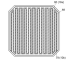
- FIG. 2 is a schematic plan view for explaining the shapes of the p-type semiconductor layer forming region and the n-type semiconductor layer forming region in the back contact solar cell. It is the figure seen from the surface side.
- FIG. 1 is a schematic cross-sectional view of a back contact solar cell according to an embodiment of the present invention, and corresponds to a cross section in the left-right direction of FIG. The arrows in FIG. 1 indicate the incident direction of sunlight. That is, the lower side (second main surface) in FIG. 1 is a light receiving surface that receives sunlight, and the upper side (first main surface) is the back surface of the solar cell.
- the lower side (second main surface) in FIG. 1 is a light receiving surface that receives sunlight
- the upper side (first main surface) is the back surface of the solar cell.
- the formation region 60 of the p-type semiconductor layer 6 and the formation region 70 of the n-type semiconductor layer 7 are provided in a comb shape that meshes with each other.
- the p-type semiconductor layer formation region and the n-type semiconductor layer formation region do not need to be comb-shaped, and may be, for example, a shape in which a portion that connects comb teeth (a so-called bus bar portion) is not provided.
- a protective layer 8 is provided in a boundary region (protective layer forming region 80) where the p-type semiconductor layer forming region and the n-type semiconductor layer forming region overlap.
- intrinsic silicon-based layers 5 a and 5 b, p-type semiconductor layer 6, n-type semiconductor layer 7, protective layer 8, and first electrode are formed on the first main surface of crystalline silicon substrate 1.
- 9a, 9b and second electrodes 10a, 10b are provided. Each layer on the first major surface is patterned.
- the n-type semiconductor layer 7 includes a protective layer formation region 80 which is a part of a region where the p-type semiconductor layer 6 is provided (p-type semiconductor layer formation region 60) and a region where the p-type semiconductor layer is not provided (p Type semiconductor layer non-formation region). That is, the n-type semiconductor layer 7 is provided so as to straddle the entire p-type semiconductor layer non-formation region and two p-type semiconductor layer formation regions adjacent to the p-type semiconductor layer non-formation region.
- the region where the p-type semiconductor layer forming region 60 and the n-type semiconductor layer forming region 70 overlap is the protective layer forming region 80, and the p-type semiconductor layer 6 and the n-type semiconductor A protective layer 8 is provided between the layer 7.
- the protective layer 8 includes a base protective layer 8b provided in contact with the p-type semiconductor layer 7 and an insulating layer 8a in this order from the p-type semiconductor layer 7 side.
- the insulating layer 8a is preferably provided in contact with the base protective layer 8b.
- the base protective layer 8b includes at least one of an intrinsic silicon-based layer and an n-type silicon-based layer.
- the base protective layer 8b may have a stacked structure of an intrinsic silicon-based layer and an n-type silicon-based layer.
- P-side electrodes 9 a and 9 b are provided on the p-type semiconductor layer 6, and n-side electrodes 9 b and 10 b are provided on the n-type semiconductor layer 7.
- the width of the p-type semiconductor layer forming region 60 and the width of the n-type semiconductor layer forming region 70 are not particularly limited, and may be equal to or different from each other. Further, the widths of these regions may differ depending on the location.
- the width of the protective layer formation region 80 (region where the p-type semiconductor layer formation region and the n-type semiconductor layer formation region overlap) is not particularly limited.
- the width W3 of the protective layer forming region 80 is set to about 10 to 500 ⁇ m, for example.
- the width W1 of the region excluding the protective layer forming regions at both ends from the p-type semiconductor layer forming region 60 and the width W2 of the region excluding the protective layer forming regions at both ends from the n-type semiconductor layer forming region 70 are, for example, 100 to 1500 ⁇ m. Set to degree.
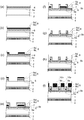
- FIG. 3 is a process conceptual diagram for explaining a manufacturing process of the back contact solar cell shown in FIG. Below, with reference to these figures, the manufacturing process of the solar cell which concerns on one Embodiment of this invention is demonstrated.
- a crystalline silicon substrate 1 is prepared.
- the crystalline silicon substrate may be either single crystal silicon or polycrystalline silicon.
- the conductivity type of the crystalline silicon substrate may be either n-type or p-type. In the examples described later, an example using an n-type single crystal silicon substrate is shown.
- the crystalline silicon substrate 1 preferably has a texture structure formed on the surface. The texture may be formed on either the first main surface or the second main surface, or may be formed on both surfaces.
- a p-type semiconductor layer forming region in which a p-type semiconductor layer 6 and a protective layer 8 are provided in this order on the first main surface of the crystalline silicon substrate 1, a p-type semiconductor layer, A p-type semiconductor layer non-formation region in which none of the protective layers is provided is formed.
- an intrinsic silicon-based layer 5 a is preferably provided between the crystalline silicon substrate 1 and the p-type semiconductor layer 6.
- the p-type semiconductor layer 6 is a layer to which a p-type dopant is added, and is preferably a p-type silicon-based layer to which boron is added.
- a p-type amorphous silicon layer is particularly preferable from the viewpoint of suppressing impurity diffusion and reducing the series resistance.
- a minute amount of microcrystalline silicon having a particle size of about 50 nm or less may be precipitated.
- the film thickness of the p-type semiconductor layer 6 is not particularly limited, and is set to about 3 to 50 nm, for example.
- the film thickness in this specification means the thickness in the direction perpendicular to the film forming surface.
- the main surface is flat, it means the thickness in the direction perpendicular to the main surface, and when the main surface has a texture structure, it means the thickness in the direction perpendicular to the texture slope.
- the film thickness of each layer can be measured by spectroscopic ellipsometry.
- the intrinsic silicon-based layer 5a is preferably intrinsic amorphous silicon composed of silicon and hydrogen.
- intrinsic hydrogenated amorphous silicon By depositing intrinsic hydrogenated amorphous silicon on the crystalline silicon substrate 1 by the CVD method, surface passivation can be effectively performed while suppressing impurity diffusion into the crystalline silicon substrate. Since the intrinsic silicon-based layer does not directly contribute to power generation, the thickness thereof is set in a range where a passivation effect can be obtained, and is preferably about 1 to 50 nm, more preferably about 1 to 15 nm.
- a region corresponding to the p-type semiconductor layer non-forming region is used as a mask.
- Examples include a method of shielding and sequentially forming each layer in the p-type semiconductor layer forming region; and a method of patterning each layer formed on substantially the entire surface of the crystalline silicon substrate 1 by etching or the like.
- a p-type semiconductor layer 6 is formed on substantially the entire surface of the crystalline silicon substrate 1 on the first main surface side.
- the intrinsic silicon-based layer 5 a is preferably formed between the crystalline silicon substrate 1 and the p-type semiconductor layer 6.
- substantially the entire surface means 90% or more of the main surface.
- Intrinsic silicon-based layer 5a and p-type semiconductor layer 6 are preferably formed in a region of 95% or more on the first main surface, and are preferably formed over the entire surface. Note that the entire surface means the entire region excluding the exception of the minimum area such as film formation unevenness at the edge of the substrate and pinholes due to discharge abnormality during film formation.
- a base protective layer 8b and an insulating layer 8a are formed on the p-type semiconductor layer 6 as the protective layer 8 in this order from the p-type semiconductor layer side.
- the insulating layer 8a is not particularly limited as long as it has insulating properties and can suppress leakage between the p-type semiconductor layer 6 and the n-type semiconductor layer 7 in the p-type semiconductor layer formation region. Since the patterning by etching is easy, the insulating layer 8a preferably includes a silicon alloy such as silicon oxide, silicon nitride, or silicon oxynitride, and preferably includes any one of these components as a main component.
- the phrase “main component” means that the content is more than 50% by weight. Among these, 70% by weight or more is preferable, and 85% by weight or more is more preferable.
- the insulating layer 8a is preferably composed of a silicon oxide layer, a silicon nitride layer, a silicon oxynitride layer, or a laminate thereof. Among these, silicon oxide is particularly preferable from the viewpoint of easy etching.
- the protective layer 8 for the p-type semiconductor layer is provided with the base protective layer 8b in contact with the p-type semiconductor layer 6 in addition to the insulating layer 8a.
- the base protective layer 8b has at least one of an intrinsic silicon-based layer and an n-type silicon-based layer.
- an intrinsic silicon-based layer an intrinsic amorphous silicon-based layer is preferable, and intrinsic amorphous silicon is particularly preferable.
- an n-type amorphous silicon-based layer is preferable, and n-type amorphous silicon is particularly preferable.
- the base protective layer 8b is also made of intrinsic silicon from the viewpoint of providing a leakage suppressing effect between the p-type semiconductor layer 6 and the n-type semiconductor layer 7 in the p-type semiconductor layer formation region.
- a system layer is particularly preferable.
- the film thickness of the base protective layer 8b is not particularly limited as long as it covers the p-type semiconductor layer 6, and is set to about 1 to 50 nm, for example.
- the film thickness of the protective layer 8, that is, the total film thickness of the base protective layer 8 b and the insulating layer 8 a is within a range in which the insulation between the p-type semiconductor layer 6 and the n-type semiconductor layer 7 can be maintained by the protective layer 8. For example, the thickness is set to about 5 to 300 nm.
- Both the intrinsic silicon-based layer and the n-type silicon-based layer can be etched with an alkaline etchant, and have an etching resistance to an acid-based etchant such as hydrofluoric acid.
- the p-type semiconductor layer 6 and the insulating layer 8a can be etched with an acid-based etchant and have an etching resistance to an alkaline etchant. Therefore, it is possible to easily perform selective etching of the insulating layer 8a and the base protective layer 8b in the protective layer patterning step described later.
- the etching resistance of the p-type semiconductor layer 6 is high when etching the base protective layer 8b using the alkaline etchant, and the deterioration of the p-type semiconductor layer is suppressed. it can.
- P-type semiconductor layer patterning process As shown in FIG. 3C, a part of the protective layer 8 is removed by etching (p layer exposure patterning step). The region where the protective layer 8 is removed corresponds to the p-type semiconductor layer non-forming region. Thereby, a protective layer forming region where the protective layer 8 remains and a protective layer non-forming region where the protective layer is removed are formed. The p-type semiconductor layer is exposed in the protective layer non-formation region.
- a method for removing a part of the protective layer for example, there is a method in which the surface of the region where the protective layer is to remain is covered (protected) with a mask, a resist or the like, and then the region other than the covered region (non-protected region) is etched. Can be mentioned.
- the p-type semiconductor layer 6 exposed between the protective layers and the intrinsic silicon provided therebelow is removed.
- the system layer 5a is removed by etching, and the first main surface of the crystalline silicon substrate 1 is exposed.
- the p-type semiconductor layer forming region where the p-type semiconductor layer 6 (and the intrinsic silicon-based layer 5a) remains, and the p-type semiconductor layer non-depleted from which the p-type semiconductor layer (and the intrinsic silicon-based layer 5a) are removed.
- a formation region is formed.
- an etchant for removing the insulating layer 8a is preferably an acid-based etchant such as a hydrofluoric acid aqueous solution.
- an etchant for removing the p-type semiconductor layer one having hydrofluoric acid is preferable, and a mixed acid of hydrofluoric acid and nitric acid is particularly preferably used.
- ⁇ Washing process> As shown in FIG. 3D, after forming the pattern layer in which the p-type semiconductor layer 6 and the protective layer 8 are stacked, the crystalline silicon substrate 1 is exposed in the p-type semiconductor layer non-formation region.
- a film, an etchant, or the like removed by etching is present on the surface of the protective layer 8 in the p-type semiconductor layer formation region or the surface of the crystalline silicon substrate in the p-type semiconductor layer non-formation region. It may be attached. Therefore, it is preferable to carry out a substrate cleaning step after forming the pattern layer and before forming the n-type semiconductor layer.
- the cleaning liquid used in the cleaning process is not particularly limited as long as the surface of the crystalline silicon substrate can be cleaned. Since the surface cleaning effect of the crystalline silicon substrate is high, it is preferable to use an aqueous solution containing hydrofluoric acid as the cleaning liquid. When cleaning is performed using an aqueous solution containing hydrofluoric acid, the insulating layer 8a is etched with hydrofluoric acid. Therefore, it is preferable to form the insulating layer 8a thick beforehand in consideration of the etching amount.
- the n-type semiconductor layer 7 is formed so as to cover the entire surface of the p-type semiconductor layer forming region and the p-type semiconductor layer non-forming region.
- the n-type semiconductor layer 7 is a layer to which an n-type dopant is added, and is preferably an n-type silicon-based layer to which phosphorus is added.
- an n-type amorphous silicon-based layer is more preferable, and n-type amorphous silicon is particularly preferable.
- the film thickness of the n-type semiconductor layer 7 is not particularly limited, and is set to about 3 to 50 nm, for example.
- An intrinsic silicon-based layer 5 b is preferably provided between the crystalline silicon substrate 1 and the p-type semiconductor layer 6.
- intrinsic silicon-based layer 5b intrinsic hydrogenated amorphous silicon composed of silicon and hydrogen is preferable.
- the film thickness and composition of the intrinsic silicon-based layer 5 b may be the same as or different from the intrinsic silicon-based layer 5 a provided under the p-type semiconductor layer 6.
- n-type semiconductor layer patterning process As shown in FIG. 3F, a part of the n-type semiconductor layer 7 on the protective layer 8 is removed by etching.
- the intrinsic silicon-based layer 5 b When the intrinsic silicon-based layer 5 b is provided between the protective layer 8 and the n-type semiconductor layer 7, the intrinsic silicon-based layer 5 b is also removed in the same manner as the n-type semiconductor layer 7.
- the n-type semiconductor layer is etched, the surface of the region where the n-type semiconductor layer should be left is covered with a mask, a resist, or the like, thereby protecting it from the etchant.
- An alkaline etchant containing KOH or NaOH is preferably used to remove the n-type semiconductor layer 7 and the intrinsic silicon-based layer 5b.
- the n-type semiconductor layer 7 and the intrinsic silicon-based layer 5b in the center in the width direction of the region where the p-type semiconductor layer 6 and the protective layer 8 are provided are removed. Is done. As a result, the protective layer 8 is exposed between the n-type semiconductor layers 7. In the region where the n-type semiconductor layer 7 remains in the p-type semiconductor layer formation region, that is, in the region where both the p-type semiconductor layer 6 and the n-type semiconductor layer are provided, the p-type semiconductor layer 6 and the n-type semiconductor are formed. Since the protective layer 8 is provided between the layer 7 and the pn, leakage between pn is suppressed.
- the base protective layer 8b is exposed between the insulating layers 8a.
- the base protective layer 8b exposed between the insulating layers 8a is removed by etching, so that the n-type semiconductor layers 7 are interposed.
- the p-type semiconductor layer 6 is exposed.
- the etchant for removing the insulating layer 8a may be any one that has little damage to the n-type semiconductor layer 7 and the like exposed in the p-type semiconductor layer non-formation region.
- As the etchant for removing the base protective layer 8b What is necessary is just to have little damage to the p-type semiconductor layer 6 and the like provided thereunder.
- As the etchant for removing the insulating layer 8a it is preferable to use an etchant that has an etching rate with respect to the insulating layer larger than that with respect to the base protective layer and does not substantially dissolve the base protective layer.
- the etchant for removing the base protective layer 8b it is preferable to use an etchant that has an etching rate with respect to the base protective layer higher than that with respect to the p-type semiconductor layer and does not substantially dissolve the p-type semiconductor layer.
- the etchant for removing the base protective layer 8b preferably has an etching rate with respect to the base protective layer larger than that with respect to the insulating layer and does not substantially dissolve the insulating layer.
- the insulating layer 8a is composed of silicon oxide, silicon nitride, silicon oxynitride, or a laminate thereof, it is preferable to use an acid-based etchant such as hydrofluoric acid for removing the insulating layer 8a.
- an acid-based etchant such as hydrofluoric acid for removing the insulating layer 8a.
- Silicon oxide, silicon nitride, silicon oxynitride, or the like has a high etching rate with respect to an acid-based etchant and a low etching rate with respect to an alkali-based etchant such as Na0H or KOH.
- intrinsic silicon and n-type silicon constituting the base protective layer 8b have a low etching rate with respect to the acid-based etchant, and thus are not substantially etched with the acid-based etchant. Therefore, if the insulating layer 8a is etched using an acid-based etchant, the etching stops when the base protective layer 8b is exposed, and selective etching becomes possible.
- the base protective layer 8b After etching the insulating layer 8a, it is preferable to etch the base protective layer 8b using an alkaline etchant. Since the alkaline etchant has a high etching rate with respect to intrinsic silicon and n-type silicon, the base protective layer 8b can be easily etched with the alkaline etchant. On the other hand, the p-type semiconductor layer 6 has a low etching rate with respect to the alkaline etchant. When the alkaline etchant is used, the etching stops when the p-type semiconductor layer 6 is exposed. Therefore, the base protective layer 8b is selectively etched while suppressing damage to the p-type semiconductor layer, thereby forming the p-type semiconductor. The layer can be exposed.
- the alkaline etchant has a low etching rate of silicon oxide, silicon nitride, silicon oxynitride or the like of the insulating layer 8a, expansion of the region from which the insulating layer 8a is removed is suppressed during etching of the base protective layer 8b. . Therefore, the protective layer 8 in which the base protective layer 8b and the insulating layer 8a are laminated can be left between the p-type semiconductor layer 6 and the n-type semiconductor layer 7, and leakage between pn can be suppressed.
- the n-type semiconductor layer 7 is exposed on the surface of the p-type semiconductor layer non-formation region during the protective layer patterning step. If an alkaline etchant is used to remove the base protective layer 8b, the n-type semiconductor layer 7 may also be etched. In order to prevent the n-type semiconductor layer 7 from being removed by etching during the etching of the base protective layer 8b, the n-type semiconductor layer 7 is formed with a film thickness larger than that of the base protective layer 8b, or n It is preferable to protect the mold semiconductor layer 7 by covering it with a mask, a resist or the like.
- Electrode formation process After forming the semiconductor layer as described above, electrodes 9a and 10a and electrodes 9b and 10b are formed on the p-type semiconductor layer 6 and the n-type semiconductor layer 7 as shown in FIG. Electrode forming step). Through the above steps, formation of each layer on the first main surface of the back contact solar cell shown in FIG. 1 is completed.
- the insulating layer 8a is provided as a protective layer in contact with the p-type semiconductor layer 6, the p-type semiconductor layer 6 exposed by etching of the insulating layer is removed when the insulating layer is removed by etching. It is exposed to an etchant (see FIG. 4 (g)). As described above, the insulating layer 8a on the p-type semiconductor layer is etched when cleaning the surface of the substrate using hydrofluoric acid after forming the pattern layer. It is necessary to increase the thickness.
- the thickness of the insulating layer is uneven, the difference in film thickness due to the unevenness increases in proportion to the thickness of the insulating layer, resulting in a difference in etching completion time depending on the location. Therefore, even if the substrate is taken out from the etchant immediately after the etching of the insulating layer, the p-type semiconductor layer is exposed to the etchant for removing the insulating layer for a long time in a region where the thickness of the insulating layer is small. In addition, when a pinhole is generated during the formation of the insulating layer, the etchant soaked from the pinhole comes into contact with the p-type semiconductor layer.
- the p-type semiconductor material such as p-type amorphous silicon has lower resistance to acid-based etchants such as hydrofluoric acid than the intrinsic semiconductor material and the n-type semiconductor material.
- acid-based etchants such as hydrofluoric acid
- the characteristics of the solar cell tend to deteriorate.
- the base protective layer 8b between the p-type semiconductor layer 6 and the insulating layer 8a, the insulating layer Even if 8a is etched, the p-type semiconductor layer 6 is not exposed and can be protected from the etchant (see FIG. 3G).
- the underlying protective layer 8b functions sufficiently as a protective layer at the time of etching as long as it covers substantially the entire surface of the p-type semiconductor layer 6, and therefore may have a smaller film thickness than the insulating layer 8a.
- the base protective layer 8b is less affected by film thickness unevenness than the insulating layer 8a, and the difference in etching completion time is also small. Therefore, the contact time between the etchant used for removing the base protective layer 8b and the p-type semiconductor layer 6 can be shortened.
- an etchant for example, an alkaline etchant
- an alkaline etchant that causes less damage to the p-type semiconductor layer than hydrofluoric acid or the like for removing the insulating layer 8a
- the base protective layer 8b is made of a material different from that of the insulating layer 8a, the base protective layer 8b is formed in a separate process from the insulating layer 8a. Even if a pinhole occurs during film formation, it is unlikely that a pinhole is formed at the same position as the base protective layer 8b in the insulating layer 8a, and the p-type semiconductor layer 6 is connected to the p-type semiconductor layer 6 via the pinhole during etching of the insulating layer. The etchant penetration can be greatly reduced. Therefore, by providing the base protective layer 8b between the p-type semiconductor layer 6 and the insulating layer 8a, it is possible to greatly reduce the probability of a short circuit between pn due to pinholes and further improve the characteristics of the solar cell. Be expected.
- the second main surface which is the light receiving surface, does not directly contribute to power generation and current extraction. Therefore, the configuration on the second main surface is not particularly limited as long as it does not hinder the reception of sunlight.
- an intrinsic silicon-based layer 2 a conductive semiconductor layer 3, and a light-receiving surface side protective layer 4 are provided in this order on the second main surface of the crystalline silicon substrate 1.
- An intrinsic silicon-based layer 2 is preferably formed on the second main surface of the crystalline silicon substrate 1 (FIG. 3A).
- the intrinsic silicon-based layer 2 is preferably an amorphous silicon layer containing hydrogen.
- substrate surface passivation can be effectively performed. Since the intrinsic silicon-based layer 2 does not contribute to power generation, it is preferable to set the film thickness so that the passivation effect is obtained without preventing light reception.
- the thickness of the intrinsic silicon-based layer 2 is preferably about 1 to 50 nm, and more preferably about 1 to 15 nm.
- a light-receiving surface side protective layer 4 that also functions as an antireflection layer is formed on the intrinsic silicon-based layer 2 (FIG. 3B). If the light-receiving surface side protective layer 4 can protect a layer (for example, the intrinsic silicon-based layer 2 or the conductive semiconductor layer 3) existing thereunder in the manufacturing process of the solar cell and has light transmittance,
- the material is not particularly limited.
- a silicon alloy such as silicon oxide, silicon nitride, or silicon oxynitride, a mixture thereof, or a laminated structure is preferable.
- silicon nitride is particularly preferable from the viewpoint of antireflection and resistance to etchant.
- the film thickness of the light-receiving surface side protective layer 4 is not particularly limited, but it is preferable to set the film thickness from the viewpoint of providing an antireflection function and increasing the amount of light taken into the crystalline silicon substrate 1, and is approximately 80 nm to 1 ⁇ m. preferable.
- a conductive semiconductor layer 3 may be formed between the intrinsic silicon-based layer 2 and the light-receiving surface side protective layer 4 (FIG. 3B).
- Conductive semiconductor layer 3 preferably has the same conductivity type as crystalline silicon substrate 1.
- an n-type semiconductor layer is preferably formed as the conductive semiconductor layer 3.
- the conductive semiconductor layer 3 is preferably a silicon-based layer, and more preferably amorphous silicon.
- the film thickness of the conductive semiconductor layer 3 is set to about 1 to 50 nm, for example.
- a plasma CVD method is preferable.
- the intrinsic silicon layer 5a and the p-type semiconductor layer 6, the intrinsic silicon layer 5b and the n-type semiconductor layer 7, and the light receiving surface side Since the intrinsic silicon-based layer 2 and the conductive semiconductor layer 3 can be successively formed, simplification of the process and prevention of contamination can be expected. Further, since the film quality of the plasma CVD method can be controlled relatively easily depending on the film forming conditions, the effect as a protective layer and the reduction of optical loss can be expected by adjusting the etching resistance and the refractive index.
- a substrate temperature of 100 to 300 ° C., a pressure of 20 to 2600 Pa, and a high frequency power density of 0.004 to 0.8 W / cm 2 are preferably used.
- a silicon-containing gas such as SiH 4 or Si 2 H 6 or a mixed gas of a silicon-based gas and H 2 is preferable.
- a dopant gas for forming the p-type or n-type silicon-based layer B 2 H 6 or PH 3 is preferably used. Since the addition amount of impurities such as P and B may be small, it is preferable to use a mixed gas diluted with SiH 4 or H 2 in advance.
- a gas containing a different element such as CH 4 , CO 2 , NH 3 , GeH 4 is added, and the silicon-based thin film is alloyed, so that the energy gap of the silicon-based layer is increased. It can also be changed.
- the method for forming the insulating layer 8a is not particularly limited.
- the insulating layer 8a is also preferably formed by the plasma CVD method from the viewpoint of improving productivity and reducing impurities.
- the light-receiving surface side protective layer 4 is preferably formed by a plasma CVD method.
- a p-side electrode is formed on the p-type semiconductor layer 6, and an n-side electrode is formed on the n-type semiconductor layer 7.
- the p-side electrode and the n-side electrode preferably have a laminated structure of a transparent conductive film as the first electrodes 9a and 9b and a metal layer as the second electrodes 10a and 10b, respectively.
- the transparent conductive film as the first electrode preferably contains a conductive oxide as a main component.
- a conductive oxide for example, zinc oxide, indium oxide, tin oxide or the like can be used alone or in combination. From the viewpoints of conductivity, optical characteristics, and long-term reliability, indium oxides containing indium oxide as the main component are preferable, and those containing indium tin oxide (ITO) as the main component are more preferably used.
- the transparent conductive film may be a single layer or a laminated structure composed of a plurality of layers.
- the film thickness of the first electrodes 9a and 9b is not particularly limited, and is set to, for example, about 10 to 100 nm.
- a method for forming the transparent conductive film is not particularly limited, but a physical vapor deposition method such as a sputtering method, a chemical vapor deposition (MOCVD) method using a reaction between an organometallic compound and oxygen or water is preferable. In any film forming method, energy by heat or plasma discharge can be used.
- the substrate temperature at the time of forming the transparent conductive film is appropriately set. Considering the heat resistant temperature of the silicon-based layer such as amorphous silicon, the substrate temperature is preferably 200 ° C. or lower.
- a metal such as Ag or Cu is used for the metal layer as the second electrode.
- the metal layer is formed by sputtering, printing, plating, or the like.
- the metal layer may be a single layer or a laminated structure including a plurality of layers.
- the thickness of the metal layer is not particularly limited, and is set to, for example, about 50 nm to 3 ⁇ m.
- the present invention will be further compared by comparing the embodiment in which the crystalline silicon solar cell shown in FIG. 1 is manufactured by the process shown in FIG. 3 and the comparative example in which the crystalline silicon solar cell is manufactured by the step shown in FIG. This will be specifically described.
- this invention is not limited to the following Example.
- n-type single crystal silicon substrate having an incident plane orientation of (100) and a thickness of 200 ⁇ m is immersed in a 2 wt% hydrofluoric acid aqueous solution for 3 minutes to remove the silicon oxide film on the surface, and then rinsed with ultrapure twice. It was broken.
- This substrate was immersed in a 5/15 wt% KOH / isopropyl alcohol aqueous solution maintained at 70 ° C. for 15 minutes to obtain a single crystal silicon substrate having a pyramidal texture with the (111) plane exposed on the surface. It was.
- the substrate after texture formation was introduced into a CVD apparatus, and an intrinsic amorphous silicon layer was formed to a thickness of 10 nm as the intrinsic silicon-based layer 2 on the light receiving surface (second main surface) side. Thereafter, an intrinsic amorphous silicon layer having a thickness of 8 nm was formed as the intrinsic silicon-based layer 5a on the back surface (first main surface) side.
- the film forming conditions for these intrinsic amorphous silicon layers were: substrate temperature: 150 ° C., pressure: 120 Pa, SiH 4 / H 2 flow rate ratio: 3/10, and input power density: 0.011 W / cm 2 .
- the film thickness of the thin film in a present Example measures the film thickness of the thin film formed on the glass substrate on the same conditions by the spectroscopic ellipsometry (brand name M2000, JA Woollam Co., Ltd. product). It is a value calculated from the film forming speed obtained by this.
- a p-type amorphous silicon layer having a thickness of 7 nm was formed as the p-type semiconductor layer 6 on the intrinsic silicon-based layer 5a.
- the conditions for forming the p-type amorphous silicon layer were as follows: the substrate temperature was 150 ° C., the pressure was 60 Pa, the SiH 4 / dilution B 2 H 6 flow rate ratio was 1/3, and the input power density was 0.01 W / cm 2 . .
- the diluted B 2 H 6 gas flow rate is a flow rate of gas diluted with H 2 to a B 2 H 6 concentration of 5000 ppm.
- a silicon nitride layer having a thickness of 60 nm was formed on the intrinsic silicon-based layer 2 as the light-receiving surface side protective layer 4. Thereafter, an intrinsic amorphous silicon layer having a thickness of 12 nm was formed as a base protective layer 8b on the p-type semiconductor layer 6, and a silicon oxide layer having a thickness of 260 nm was formed thereon as an insulating layer 8a. .
- the film forming conditions for the silicon nitride layer were: substrate temperature: 140 ° C., pressure: 80 Pa, SiH 4 / NH 3 flow rate ratio: 1/4, input power density: 0.2 W / cm 2 .
- the film formation conditions for the silicon oxide layer were a substrate temperature of 150 ° C., a pressure of 60 Pa, a SiH 4 / CO 2 flow ratio of 1/40, and an input power density of 0.04 W / cm 2 .
- a part of the insulating layer 8a was etched with an aqueous HF solution, and then a part of the intrinsic amorphous silicon layer as the underlying protective layer 8b exposed under the insulating layer 8a was removed by etching with an aqueous KOH solution. Thereafter, the p-type semiconductor layer 6 and the intrinsic silicon-based layer 5a exposed therebelow were etched with a mixed acid of HF and HNO 3 to expose the first main surface of the crystalline silicon substrate.
- an intrinsic amorphous silicon layer is formed as an intrinsic silicon-based layer 5b on the first main surface side of the substrate to a thickness of 8 nm.
- An n-type amorphous silicon layer having a thickness of 12 nm was formed as the type semiconductor layer 7.
- the film forming conditions for the n-type amorphous silicon layer were a substrate temperature of 150 ° C., a pressure of 60 Pa, a SiH 4 / dilution PH 3 flow rate ratio of 1/3, and an input power density of 0.01 W / cm 2 .
- the diluted PH 3 gas flow rate is a flow rate of a gas diluted with H 2 to a PH 3 concentration of 5000 ppm.
- the n-type semiconductor layer 7 and a part of the intrinsic silicon-based layer 5b provided on the insulating layer 8a were etched with a KOH aqueous solution, and then the insulating layer 8a exposed thereunder was etched with an HF aqueous solution. Thereafter, the intrinsic amorphous silicon layer as the underlying protective layer 8b exposed thereunder was removed by etching with an aqueous KOH solution, and the surface of the p-type semiconductor layer 6 was exposed.
- an indium tin oxide (ITO) layer having a thickness of 80 nm was formed on substantially the entire surface excluding the peripheral edge of the first main surface.
- ITO indium tin oxide
- a film was formed by applying a power of 0.5 W / cm 2 in an argon atmosphere at a substrate temperature of room temperature and a pressure of 0.2 Pa.
- a portion of the ITO layer was removed by etching using hydrochloric acid and patterned to separate the first electrodes 9a and 9b.
- the FF curve factor
- the hydrofluoric acid etchant used when etching the silicon oxide layer as the insulating layer does not contact the p-type semiconductor layer, so that the p-type amorphous silicon layer as the p-type semiconductor layer and the first electrode are used as the first electrode. This is thought to be related to improved contact with the ITO layer.
- the protective layer has a laminated structure of an intrinsic amorphous silicon layer as a base protective layer and a silicon oxide layer as an insulating layer, a reduction in leakage current between pn contributes to improvement in characteristics. It is thought that there is.
Landscapes
- Photovoltaic Devices (AREA)
- Life Sciences & Earth Sciences (AREA)
- Engineering & Computer Science (AREA)
- Sustainable Energy (AREA)
- Sustainable Development (AREA)
Abstract
Description
<パターン層形成工程>
図3(d)に示すように、結晶シリコン基板1の第一主面上に、p型半導体層6及び保護層8がこの順に設けられたp型半導体層形成領域と、p型半導体層及び保護層のいずれも設けられていないp型半導体層非形成領域とが形成される。p型半導体層形成領域では、結晶シリコン基板1とp型半導体層6との間に、真性シリコン系層5aが設けられることが好ましい。
図3(a)に示すように、結晶シリコン基板1の第一主面側の略全面にp型半導体層6が形成される。前述のように、結晶シリコン基板1とp型半導体層6との間には、真性シリコン系層5aが形成されることが好ましい。ここで、「略全面」とは、主面の90%以上を意味する。真性シリコン系層5a及びp型半導体層6は、第一主面上の95%以上の領域に形成されることが好ましく、全面に形成されることが好ましい。なお、全面とは、製膜時の放電異常等による基板端部の製膜ムラやピンホール等の極小面積の例外を除いた全領域を意味する。
次に、図3(b)に示すように、p型半導体層6上に、保護層8として、p型半導体層側から順に、下地保護層8b及び絶縁層8aが形成される。絶縁層8aは、絶縁性を有し、p型半導体層形成領域におけるp型半導体層6とn型半導体層7とのリークを抑制できるものであれば、その材料は特に限定されない。エッチングによるパターニングが容易であることから、絶縁層8aは、酸化シリコン、窒化シリコン、酸窒化シリコン等のシリコン合金を含むことが好ましく、これらの成分のいずれかを主成分とすることが好ましい。なお、本明細書において「主成分とする」とは、含有量が50重量%よりも多いことを意味する。中でも70重量%以上が好ましく、85重量%以上がより好ましい。絶縁層8aは、酸化シリコン層、窒化シリコン層、酸窒化シリコン層又はそれらの積層物から構成されることが好ましい。中でも、エッチング加工の容易さの点から、酸化シリコンが特に好ましい。
図3(c)に示すように、保護層8の一部をエッチングにより除去する(p層露出パターニング工程)。保護層8が除去される領域は、p型半導体層非形成領域に対応している。これにより、保護層8が残存している保護層形成領域と、保護層が除去された保護層非形成領域が形成される。保護層非形成領域では、p型半導体層が露出する。保護層の一部を除去する方法としては、例えば、保護層を残存させるべき領域の表面をマスクやレジスト等により被覆(保護)した後、被覆領域以外(非保護領域)をエッチングする方法等が挙げられる。
図3(d)に示すように、p型半導体層6と保護層8とが積層されたパターン層を形成後は、p型半導体層非形成領域において結晶シリコン基板1が露出している。エッチングにより各層のパターニングを実施した場合は、p型半導体層形成領域における保護層8の表面や、p型半導体層非形成領域の結晶シリコン基板の表面に、エッチングにより除去された膜やエッチャント等が付着している可能性がある。そのため、パターン層形成後、n型半導体層形成前に、基板の洗浄工程を実施することが好ましい。洗浄工程に用いられる洗浄液は、結晶シリコン基板の表面を清浄化可能であれば特に限定されない。結晶シリコン基板の表面洗浄効果が高いことから、洗浄液としてフッ酸を含有する水溶液を用いることが好ましい。フッ酸を含有する水溶液を用いて洗浄を行う場合、絶縁層8aがフッ酸によってエッチングされるため、エッチング量を考慮して、絶縁層8aを予め厚く形成しておくことが好ましい。
図3(e)に示すように、p型半導体層形成領域及びp型半導体層非形成領域の全面を覆うように、n型半導体層7が形成される。n型半導体層7はn型のドーパントが添加された層であり、リンが添加されたn型シリコン系層であることが好ましい。中でもn型非晶質シリコン系層がより好ましく、n型非晶質シリコンが特に好ましい。n型半導体層7の膜厚は特に限定されず、例えば3~50nm程度に設定される。結晶シリコン基板1とp型半導体層6との間には、真性シリコン系層5bが設けられることが好ましい。真性シリコン系層5bとしては、シリコンと水素で構成される真性水素化非晶質シリコンが好ましい。真性シリコン系層5bの膜厚や組成は、p型半導体層6の下に設けられる真性シリコン系層5aと同一でもよく、異なっていてもよい。
図3(f)に示すように、保護層8上のn型半導体層7の一部をエッチングによって除去する。保護層8とn型半導体層7との間に真性シリコン系層5bが設けられている場合は、真性シリコン系層5bもn型半導体層7と同様に除去される。n型半導体層をエッチングする際は、n型半導体層を残存させるべき領域の表面をマスクやレジスト等により被覆することにより、エッチャントから保護する。n型半導体層7及び真性シリコン系層5bの除去には、KOHやNaOHを含むアルカリ系エッチャントが好ましく用いられる。
n型半導体層パターニング工程後、図3(g)及び(h)に示すように、n型半導体層が除去された領域に露出した保護層8をエッチングにより除去する。これにより、n型半導体層7の間にp型半導体層6が露出する。この際、p型半導体層6が露出し、かつp型半導体層形成領域上の保護層8が残存していればよい。好ましくは、n型半導体層の間に露出している保護層の全部が除去される。
上記の様に半導体層を形成後、図3(i)に示すように、p型半導体層6及びn型半導体層7上のそれぞれに電極9a,10a、及び電極9b,10bが形成される(電極形成工程)。以上の工程により、図1に示すバックコンタクト型太陽電池の第一主面上の各層の形成が完了する。
図4に示すように、p型半導体層6に接する保護層として絶縁層8aが設けられている場合は、エッチングによる絶縁層除去の際に、絶縁層のエッチングにより露出したp型半導体層6がエッチャントに曝される(図4(g)参照)。前述のように、p型半導体層上の絶縁層8aは、パターン層形成後のフッ酸を用いた基板の表面洗浄の際にエッチングされるため、pn間の絶縁性確保の観点から、製膜厚みを大きくしておく必要がある。絶縁層の製膜厚みにムラがある場合、製膜厚みに比例してムラによる膜厚差が拡大するため、場所によってエッチング完了時間に差が生じる。そのため、絶縁層のエッチング完了後すぐにエッチャントから基板を取り出したとしても、絶縁層の製膜厚みが小さい領域では、p型半導体層が、絶縁層除去のためのエッチャントに長時間曝される。また、絶縁層の製膜時にピンホールが生じている場合、ピンホールから染み込んだエッチャントがp型半導体層に接触する。上記のように、p型非晶質シリコン等のp型半導体材料は、真性半導体材料やn型半導体材料に比べて、フッ酸等の酸系エッチャントに対する耐性が低いため、p型半導体層6が、絶縁層除去のためのエッチャントに曝されると、太陽電池の特性が低下する傾向がある。
バックコンタクト型太陽電池において、受光面である第二主面は、発電及び電流の取り出しには直接寄与しない。そのため、第二主面上の構成は、太陽光の受光を妨げない限り、特に制限はない。図1に示す太陽電池では、結晶シリコン基板1の第二主面上に、真性シリコン系層2、導電型半導体層3及び受光面側保護層4がこの順に設けられている。
上述のp型シリコン系層、n型シリコン系層、真性シリコン系層等のシリコン系層の製膜方法としては、プラズマCVD法が好ましい。真性シリコン系層と導電型シリコン系層をいずれもプラズマCVD法によって製膜する場合、真性シリコン系層5aとp型半導体層6、真性シリコン系層5bとn型半導体層7、受光面側の真性シリコン系層2と導電型半導体層3を、それぞれ連続して製膜できるため、工程の簡略化や汚染防止が期待できる。また、プラズマCVD法は、製膜条件によって比較的容易に膜質を制御できることから、耐エッチング性や屈折率を調整することにより、保護層としての効果の向上や光学的損失の低減が期待できる。
入射面方位が(100)で厚みが200μmのn型単結晶シリコン基板を、2重量%のフッ酸水溶液に3分間浸漬し、表面の酸化シリコン膜を除去後、超純粋によるリンスが2回行われた。この基板を、70℃に保持された5/15重量%のKOH/イソプロピルアルコール水溶液に15分間浸漬し、表面に(111)面が露出したピラミッド型のテクスチャが形成された単結晶シリコン基板を得た。
下地保護層8b(真性非晶質シリコン層)を形成せずに、p型半導体層6上に保護層8として酸化シリコン層のみを形成し、下地保護層8bのエッチング工程を省略した以外は、実施例と同様にして結晶シリコン太陽電池を作製した。
以上のようにして作製した実施例及び比較例の結晶シリコン太陽電池の変換特性(開放電圧Voc、電流密度Isc及び曲線因子FF)を測定した。実施例の太陽電池は、Vocが比較例の1.06倍、Iscが比較例の1.02倍、FFが比較例の1.31倍であり、すべての特性が改善していた。この結果から、p型半導体層と絶縁層との間に下地保護層を設けることにより、バックコンタクト型太陽電池の特性を向上できることがわかる。
2 真性シリコン系層
3 導電型半導体層
4 受光面側保護層
5a,5b 真性シリコン系層
6 p型半導体層
7 n型半導体層
8 保護層
8a 絶縁層
8b 下地保護層(真性シリコン系層又は/及びn型シリコン系層)
9a,9b 第一電極
10a,10b 第二電極
Claims (14)
- 結晶シリコン基板の第一主面上にn型半導体層及びp型半導体層を備える太陽電池の製造方法であって、
結晶シリコン基板の第一主面上に、p型半導体層及び保護層がこの順に設けられたp型半導体層形成領域と、p型半導体層及び保護層のいずれも設けられていないp型半導体層非形成領域とを形成する、パターン層形成工程、
前記p型半導体層形成領域と前記p型半導体層非形成領域とを覆うように、n型半導体層を形成する、n型半導体層形成工程;
前記n型半導体層の間に前記保護層が露出するように、前記n型半導体層の一部を除去する、n型半導体層パターニング工程;及び
前記n型半導体層の間に前記p型半導体層が露出するように、前記n型半導体層の間に露出した前記保護層を除去する、保護層パターニング工程、をこの順に有し、
前記保護層は、前記p型半導体層に接して設けられた下地保護層と、前記下地保護層上に設けられた絶縁層とを有し、
前記下地保護層は、真性シリコン系層及びn型シリコン系層からなる群から選択される1以上の層を有する、太陽電池の製造方法。 - 前記絶縁層が、酸化シリコン、窒化シリコン及び酸窒化シリコンからなる群から選択される1以上のシリコン合金を含有する、請求項1に記載の太陽電池の製造方法。
- 前記保護層パターニング工程において、
前記絶縁層に対するエッチングレートが前記下地保護層に対するエッチングレートよりも大きいエッチャントを用いて、前記絶縁層が除去され、
前記絶縁層を除去後に、前記下地保護層に対するエッチングレートが前記p型半導体層に対するエッチングレートよりも大きいエッチャントを用いて、前記下地保護層が除去される、請求項1又は2に記載の太陽電池の製造方法。 - 前記下地保護層の除去に用いられるエッチャントは、前記下地保護層に対するエッチングレートが前記絶縁層に対するエッチングレートよりも大きい、請求項3に記載の太陽電池の製造方法。
- 前記絶縁層の除去に用いられるエッチャントが酸系エッチャントである、請求項1~4のいずれか1項に記載の太陽電池の製造方法。
- 前記酸系エッチャントがフッ酸を含む、請求項5に記載の太陽電池の製造方法。
- 前記下地保護層の除去に用いられるエッチャントがアルカリ系エッチャントである、請求項1~6のいずれか1項に記載の太陽電池の製造方法。
- 前記アルカリ系エッチャントがKOH及びNaOHからなる群から選択される1以上を含む、請求項7に記載の太陽電池の製造方法。
- 前記下地保護層が真性シリコン系層である、請求項1~8のいずれか1項に記載の太陽電池の製造方法。
- 前記p型半導体層がp型シリコン系層である、請求項1~9のいずれか1項に記載の太陽電池の製造方法。
- 前記パターン層形成工程は、
前記結晶シリコン基板の第一主面上にp型半導体層を形成する、p型半導体層形成工程;
前記p型半導体層上に保護層を形成する、保護層形成工程;及び
前記保護層の間に露出した前記p型半導体層を除去する、p型半導体層パターニング工程、をこの順に有する、請求項1~10のいずれか1項に記載の太陽電池の製造方法。 - 前記保護層形成工程と前記p型半導体層パターニング工程との間に、前記保護層の間に前記p型半導体層が露出するように前記保護層の一部を除去する、p層露出パターニング工程をさらに有する、請求項11に記載の太陽電池の製造方法。
- 結晶シリコン基板の第一主面上にn型半導体層及びp型半導体層を備える太陽電池であって、
前記結晶シリコン基板の第一主面上において、前記n型半導体層は、前記p型半導体層が設けられたp型半導体層形成領域上の一部と、前記p型半導体層が設けられていないp型半導体層非形成領域とに跨るように設けられており、
前記p型半導体層形成領域上に前記n型半導体層が設けられている領域において、前記p型半導体層とn型半導体層の間に保護層が設けられており、
前記保護層は、前記p型半導体層に接して設けられた下地保護層と、前記下地保護層上に設けられた絶縁層とを有し、
前記下地保護層は、真性シリコン系層及びn型シリコン系層からなる群から選択される1以上の層を有する、太陽電池。 - 前記下地保護層が真性シリコン系層である、請求項13に記載の太陽電池。
Priority Applications (3)
| Application Number | Priority Date | Filing Date | Title |
|---|---|---|---|
| US15/556,469 US10854767B2 (en) | 2015-03-31 | 2016-03-07 | Solar cell and method for manufacturing same |
| CN201680004706.2A CN107210331B (zh) | 2015-03-31 | 2016-03-07 | 太阳能电池及其制造方法 |
| JP2017509449A JP6692797B2 (ja) | 2015-03-31 | 2016-03-07 | 太陽電池及びその製造方法 |
Applications Claiming Priority (2)
| Application Number | Priority Date | Filing Date | Title |
|---|---|---|---|
| JP2015074454 | 2015-03-31 | ||
| JP2015-074454 | 2015-03-31 |
Publications (1)
| Publication Number | Publication Date |
|---|---|
| WO2016158226A1 true WO2016158226A1 (ja) | 2016-10-06 |
Family
ID=57004972
Family Applications (1)
| Application Number | Title | Priority Date | Filing Date |
|---|---|---|---|
| PCT/JP2016/057042 Ceased WO2016158226A1 (ja) | 2015-03-31 | 2016-03-07 | 太陽電池及びその製造方法 |
Country Status (4)
| Country | Link |
|---|---|
| US (1) | US10854767B2 (ja) |
| JP (1) | JP6692797B2 (ja) |
| CN (1) | CN107210331B (ja) |
| WO (1) | WO2016158226A1 (ja) |
Cited By (6)
| Publication number | Priority date | Publication date | Assignee | Title |
|---|---|---|---|---|
| WO2018168180A1 (ja) * | 2017-03-17 | 2018-09-20 | 株式会社カネカ | 太陽電池およびその製造方法 |
| WO2019069643A1 (ja) * | 2017-10-04 | 2019-04-11 | 株式会社カネカ | 太陽電池の製造方法、太陽電池および太陽電池モジュール |
| JPWO2021230227A1 (ja) * | 2020-05-13 | 2021-11-18 | ||
| JP2023123356A (ja) * | 2022-02-24 | 2023-09-05 | 広東愛旭科技有限公司 | 背面接触電池の電極構造、電池、モジュール及び電池システム |
| JP2024000941A (ja) * | 2022-06-21 | 2024-01-09 | ジョジアン ジンコ ソーラー カンパニー リミテッド | 半導体基板、太陽電池及び太陽光発電モジュール |
| JP7642123B1 (ja) | 2024-02-07 | 2025-03-07 | ジョジアン ジンコ ソーラー カンパニー リミテッド | 太陽電池、太陽電池の製造方法及び光起電力モジュール |
Families Citing this family (6)
| Publication number | Priority date | Publication date | Assignee | Title |
|---|---|---|---|---|
| JPWO2019138613A1 (ja) * | 2018-01-09 | 2021-01-07 | 株式会社カネカ | 太陽電池の製造方法 |
| CN113224179A (zh) * | 2021-04-28 | 2021-08-06 | 浙江爱旭太阳能科技有限公司 | 晶体硅太阳能电池钝化层及其制备方法、电池 |
| CN113809188B (zh) * | 2021-09-13 | 2025-03-25 | 福建金石能源有限公司 | 一种采用化学蚀刻裸露第一导电区的背接触异质结太阳能电池制造方法 |
| CN114944432B (zh) * | 2022-05-05 | 2024-09-06 | 西安隆基乐叶光伏科技有限公司 | 一种hbc太阳能电池及制备方法、电池组件 |
| CN115588698B (zh) * | 2022-11-07 | 2024-11-01 | 隆基绿能科技股份有限公司 | 背接触太阳能电池及其制备方法、光伏组件 |
| CN119050206A (zh) * | 2024-09-03 | 2024-11-29 | 天合光能股份有限公司 | 背接触太阳能电池及其制备方法 |
Citations (7)
| Publication number | Priority date | Publication date | Assignee | Title |
|---|---|---|---|---|
| JP2005268683A (ja) * | 2004-03-22 | 2005-09-29 | Canon Inc | 太陽電池の製造方法および太陽電池 |
| JP2007134655A (ja) * | 2005-11-14 | 2007-05-31 | Sharp Corp | 太陽電池およびその製造方法 |
| WO2012132854A1 (ja) * | 2011-03-25 | 2012-10-04 | 三洋電機株式会社 | 光電変換装置及びその製造方法 |
| JP2013026269A (ja) * | 2011-07-15 | 2013-02-04 | Sanyo Electric Co Ltd | 太陽電池及び太陽電池の製造方法 |
| JP2013125964A (ja) * | 2011-12-13 | 2013-06-24 | Samsung Sdi Co Ltd | 光起電力素子及びその製造方法 |
| US20140096821A1 (en) * | 2012-10-10 | 2014-04-10 | Au Optronics Corp. | Solar cell and method for making thereof |
| US20140166094A1 (en) * | 2012-12-18 | 2014-06-19 | Paul Loscutoff | Solar cell emitter region fabrication using etch resistant film |
Family Cites Families (10)
| Publication number | Priority date | Publication date | Assignee | Title |
|---|---|---|---|---|
| US20100071765A1 (en) * | 2008-09-19 | 2010-03-25 | Peter Cousins | Method for fabricating a solar cell using a direct-pattern pin-hole-free masking layer |
| KR101521326B1 (ko) * | 2009-03-30 | 2015-05-18 | 산요덴키가부시키가이샤 | 태양 전지 |
| EP2530729B1 (en) * | 2010-01-26 | 2019-10-16 | Panasonic Intellectual Property Management Co., Ltd. | Solar cell and method for producing same |
| JP2011204832A (ja) * | 2010-03-25 | 2011-10-13 | Sanyo Electric Co Ltd | 太陽電池及びその製造方法 |
| JP5485060B2 (ja) | 2010-07-28 | 2014-05-07 | 三洋電機株式会社 | 太陽電池の製造方法 |
| EP2660873A4 (en) * | 2010-12-29 | 2018-03-28 | Panasonic Intellectual Property Management Co., Ltd. | Method for manufacturing solar cell and solar cell |
| WO2012132835A1 (ja) | 2011-03-25 | 2012-10-04 | 三洋電機株式会社 | 太陽電池 |
| US9054255B2 (en) * | 2012-03-23 | 2015-06-09 | Sunpower Corporation | Solar cell having an emitter region with wide bandgap semiconductor material |
| JP6179900B2 (ja) * | 2012-03-30 | 2017-08-16 | パナソニックIpマネジメント株式会社 | 太陽電池及びその製造方法 |
| JP2014075526A (ja) * | 2012-10-05 | 2014-04-24 | Sharp Corp | 光電変換素子および光電変換素子の製造方法 |
-
2016
- 2016-03-07 JP JP2017509449A patent/JP6692797B2/ja active Active
- 2016-03-07 CN CN201680004706.2A patent/CN107210331B/zh active Active
- 2016-03-07 US US15/556,469 patent/US10854767B2/en active Active
- 2016-03-07 WO PCT/JP2016/057042 patent/WO2016158226A1/ja not_active Ceased
Patent Citations (7)
| Publication number | Priority date | Publication date | Assignee | Title |
|---|---|---|---|---|
| JP2005268683A (ja) * | 2004-03-22 | 2005-09-29 | Canon Inc | 太陽電池の製造方法および太陽電池 |
| JP2007134655A (ja) * | 2005-11-14 | 2007-05-31 | Sharp Corp | 太陽電池およびその製造方法 |
| WO2012132854A1 (ja) * | 2011-03-25 | 2012-10-04 | 三洋電機株式会社 | 光電変換装置及びその製造方法 |
| JP2013026269A (ja) * | 2011-07-15 | 2013-02-04 | Sanyo Electric Co Ltd | 太陽電池及び太陽電池の製造方法 |
| JP2013125964A (ja) * | 2011-12-13 | 2013-06-24 | Samsung Sdi Co Ltd | 光起電力素子及びその製造方法 |
| US20140096821A1 (en) * | 2012-10-10 | 2014-04-10 | Au Optronics Corp. | Solar cell and method for making thereof |
| US20140166094A1 (en) * | 2012-12-18 | 2014-06-19 | Paul Loscutoff | Solar cell emitter region fabrication using etch resistant film |
Cited By (20)
| Publication number | Priority date | Publication date | Assignee | Title |
|---|---|---|---|---|
| WO2018168180A1 (ja) * | 2017-03-17 | 2018-09-20 | 株式会社カネカ | 太陽電池およびその製造方法 |
| WO2019069643A1 (ja) * | 2017-10-04 | 2019-04-11 | 株式会社カネカ | 太陽電池の製造方法、太陽電池および太陽電池モジュール |
| JPWO2019069643A1 (ja) * | 2017-10-04 | 2020-11-05 | 株式会社カネカ | 太陽電池の製造方法、太陽電池および太陽電池モジュール |
| US11177407B2 (en) | 2017-10-04 | 2021-11-16 | Kaneka Corporation | Method for manufacturing solar cell, solar cell, and solar cell module |
| JP7146786B2 (ja) | 2017-10-04 | 2022-10-04 | 株式会社カネカ | 太陽電池の製造方法、太陽電池および太陽電池モジュール |
| JPWO2021230227A1 (ja) * | 2020-05-13 | 2021-11-18 | ||
| WO2021230227A1 (ja) * | 2020-05-13 | 2021-11-18 | 株式会社カネカ | 太陽電池および太陽電池製造方法 |
| JP7756078B2 (ja) | 2020-05-13 | 2025-10-17 | 株式会社カネカ | 太陽電池および太陽電池製造方法 |
| JP2023123356A (ja) * | 2022-02-24 | 2023-09-05 | 広東愛旭科技有限公司 | 背面接触電池の電極構造、電池、モジュール及び電池システム |
| JP7401700B2 (ja) | 2022-02-24 | 2023-12-19 | 広東愛旭科技有限公司 | 背面接触電池の電極構造、電池、モジュール及び電池システム |
| JP7453283B2 (ja) | 2022-06-21 | 2024-03-19 | ジョジアン ジンコ ソーラー カンパニー リミテッド | 半導体基板、太陽電池及び太陽光発電モジュール |
| JP2024039048A (ja) * | 2022-06-21 | 2024-03-21 | ジョジアン ジンコ ソーラー カンパニー リミテッド | 半導体基板、太陽電池及び太陽光発電モジュール |
| JP7602002B2 (ja) | 2022-06-21 | 2024-12-17 | ジョジアン ジンコ ソーラー カンパニー リミテッド | 半導体基板、太陽電池及び太陽光発電モジュール |
| US12191411B2 (en) | 2022-06-21 | 2025-01-07 | Zhejiang Jinko Solar Co., Ltd. | Semiconductor substrate, solar cell, and photovoltaic module |
| JP2024000941A (ja) * | 2022-06-21 | 2024-01-09 | ジョジアン ジンコ ソーラー カンパニー リミテッド | 半導体基板、太陽電池及び太陽光発電モジュール |
| JP7642123B1 (ja) | 2024-02-07 | 2025-03-07 | ジョジアン ジンコ ソーラー カンパニー リミテッド | 太陽電池、太陽電池の製造方法及び光起電力モジュール |
| JP2025121895A (ja) * | 2024-02-07 | 2025-08-20 | ジョジアン ジンコ ソーラー カンパニー リミテッド | 太陽電池、太陽電池の製造方法及び光起電力モジュール |
| JP2025121805A (ja) * | 2024-02-07 | 2025-08-20 | ジョジアン ジンコ ソーラー カンパニー リミテッド | 太陽電池、太陽電池の製造方法及び光起電力モジュール |
| US12501720B2 (en) | 2024-02-07 | 2025-12-16 | Zhejiang Jinko Solar Co., Ltd. | Solar cell, method for manufacturing solar cell, and photovoltaic module |
| JP2026065666A (ja) * | 2024-02-07 | 2026-04-15 | ジョジアン ジンコ ソーラー カンパニー リミテッド | 太陽電池、太陽電池の製造方法及び光起電力モジュール |
Also Published As
| Publication number | Publication date |
|---|---|
| JP6692797B2 (ja) | 2020-05-13 |
| CN107210331B (zh) | 2019-06-28 |
| CN107210331A (zh) | 2017-09-26 |
| US20180069144A1 (en) | 2018-03-08 |
| JPWO2016158226A1 (ja) | 2018-01-25 |
| US10854767B2 (en) | 2020-12-01 |
Similar Documents
| Publication | Publication Date | Title |
|---|---|---|
| JP6692797B2 (ja) | 太陽電池及びその製造方法 | |
| EP2434548B1 (en) | Solar cell and method for manufacturing the same | |
| JP5705968B2 (ja) | 光電変換装置及びその製造方法 | |
| JP5820988B2 (ja) | 光電変換装置及びその製造方法 | |
| JP5774204B2 (ja) | 光起電力素子およびその製造方法、太陽電池モジュール | |
| JP5891382B2 (ja) | 光電変換素子の製造方法 | |
| KR101897723B1 (ko) | 광기전력소자 및 그 제조 방법 | |
| JP7228561B2 (ja) | 太陽電池の製造方法 | |
| JP6141670B2 (ja) | 太陽電池の製造方法 | |
| AU2024289730A1 (en) | Back contact solar cell, preparation method therefor, and photovoltaic module | |
| JP5307688B2 (ja) | 結晶シリコン系太陽電池 | |
| JP5884030B2 (ja) | 光電変換装置の製造方法 | |
| WO2018168180A1 (ja) | 太陽電池およびその製造方法 | |
| JP6136024B2 (ja) | 太陽電池の製造方法 | |
| JP7146786B2 (ja) | 太陽電池の製造方法、太陽電池および太陽電池モジュール | |
| JP7237920B2 (ja) | 太陽電池の製造方法 | |
| JP7281444B2 (ja) | 太陽電池の製造方法 | |
| JP2013115057A (ja) | 結晶シリコン太陽電池の製造方法 | |
| JP2011077454A (ja) | 結晶シリコン系太陽電池とその製造方法 | |
| JPWO2012132961A1 (ja) | 光電変換素子の製造方法 | |
| JP4641858B2 (ja) | 太陽電池 | |
| JP6143520B2 (ja) | 結晶シリコン系太陽電池およびその製造方法 | |
| WO2017203751A1 (ja) | 太陽電池及びその製造方法、並びに太陽電池パネル | |
| WO2020022044A1 (ja) | 太陽電池の製造方法 | |
| CN115440848A (zh) | 钝化接触电池及其制造方法 |
Legal Events
| Date | Code | Title | Description |
|---|---|---|---|
| 121 | Ep: the epo has been informed by wipo that ep was designated in this application |
Ref document number: 16772110 Country of ref document: EP Kind code of ref document: A1 |
|
| ENP | Entry into the national phase |
Ref document number: 2017509449 Country of ref document: JP Kind code of ref document: A |
|
| WWE | Wipo information: entry into national phase |
Ref document number: 15556469 Country of ref document: US |
|
| NENP | Non-entry into the national phase |
Ref country code: DE |
|
| 122 | Ep: pct application non-entry in european phase |
Ref document number: 16772110 Country of ref document: EP Kind code of ref document: A1 |