WO2016152059A1 - 半導体装置 - Google Patents
半導体装置 Download PDFInfo
- Publication number
- WO2016152059A1 WO2016152059A1 PCT/JP2016/001322 JP2016001322W WO2016152059A1 WO 2016152059 A1 WO2016152059 A1 WO 2016152059A1 JP 2016001322 W JP2016001322 W JP 2016001322W WO 2016152059 A1 WO2016152059 A1 WO 2016152059A1
- Authority
- WO
- WIPO (PCT)
- Prior art keywords
- insulating film
- trench
- gate
- region
- semiconductor device
- Prior art date
- Legal status (The legal status is an assumption and is not a legal conclusion. Google has not performed a legal analysis and makes no representation as to the accuracy of the status listed.)
- Ceased
Links
Images

Classifications
-
- H—ELECTRICITY
- H10—SEMICONDUCTOR DEVICES; ELECTRIC SOLID-STATE DEVICES NOT OTHERWISE PROVIDED FOR
- H10D—INORGANIC ELECTRIC SEMICONDUCTOR DEVICES
- H10D62/00—Semiconductor bodies, or regions thereof, of devices having potential barriers
- H10D62/10—Shapes, relative sizes or dispositions of the regions of the semiconductor bodies; Shapes of the semiconductor bodies
- H10D62/17—Semiconductor regions connected to electrodes not carrying current to be rectified, amplified or switched, e.g. channel regions
- H10D62/213—Channel regions of field-effect devices
- H10D62/221—Channel regions of field-effect devices of FETs
- H10D62/235—Channel regions of field-effect devices of FETs of IGFETs
- H10D62/314—Channel regions of field-effect devices of FETs of IGFETs having vertical doping variations
-
- H—ELECTRICITY
- H10—SEMICONDUCTOR DEVICES; ELECTRIC SOLID-STATE DEVICES NOT OTHERWISE PROVIDED FOR
- H10D—INORGANIC ELECTRIC SEMICONDUCTOR DEVICES
- H10D12/00—Bipolar devices controlled by the field effect, e.g. insulated-gate bipolar transistors [IGBT]
- H10D12/01—Manufacture or treatment
- H10D12/031—Manufacture or treatment of IGBTs
-
- H—ELECTRICITY
- H10—SEMICONDUCTOR DEVICES; ELECTRIC SOLID-STATE DEVICES NOT OTHERWISE PROVIDED FOR
- H10D—INORGANIC ELECTRIC SEMICONDUCTOR DEVICES
- H10D30/00—Field-effect transistors [FET]
- H10D30/01—Manufacture or treatment
- H10D30/021—Manufacture or treatment of FETs having insulated gates [IGFET]
- H10D30/028—Manufacture or treatment of FETs having insulated gates [IGFET] of double-diffused metal oxide semiconductor [DMOS] FETs
- H10D30/0291—Manufacture or treatment of FETs having insulated gates [IGFET] of double-diffused metal oxide semiconductor [DMOS] FETs of vertical DMOS [VDMOS] FETs
- H10D30/0297—Manufacture or treatment of FETs having insulated gates [IGFET] of double-diffused metal oxide semiconductor [DMOS] FETs of vertical DMOS [VDMOS] FETs using recessing of the gate electrodes, e.g. to form trench gate electrodes
-
- H—ELECTRICITY
- H10—SEMICONDUCTOR DEVICES; ELECTRIC SOLID-STATE DEVICES NOT OTHERWISE PROVIDED FOR
- H10D—INORGANIC ELECTRIC SEMICONDUCTOR DEVICES
- H10D30/00—Field-effect transistors [FET]
- H10D30/60—Insulated-gate field-effect transistors [IGFET]
-
- H—ELECTRICITY
- H10—SEMICONDUCTOR DEVICES; ELECTRIC SOLID-STATE DEVICES NOT OTHERWISE PROVIDED FOR
- H10D—INORGANIC ELECTRIC SEMICONDUCTOR DEVICES
- H10D30/00—Field-effect transistors [FET]
- H10D30/60—Insulated-gate field-effect transistors [IGFET]
- H10D30/64—Double-diffused metal-oxide semiconductor [DMOS] FETs
- H10D30/66—Vertical DMOS [VDMOS] FETs
- H10D30/668—Vertical DMOS [VDMOS] FETs having trench gate electrodes, e.g. UMOS transistors
-
- H—ELECTRICITY
- H10—SEMICONDUCTOR DEVICES; ELECTRIC SOLID-STATE DEVICES NOT OTHERWISE PROVIDED FOR
- H10D—INORGANIC ELECTRIC SEMICONDUCTOR DEVICES
- H10D62/00—Semiconductor bodies, or regions thereof, of devices having potential barriers
- H10D62/10—Shapes, relative sizes or dispositions of the regions of the semiconductor bodies; Shapes of the semiconductor bodies
-
- H—ELECTRICITY
- H10—SEMICONDUCTOR DEVICES; ELECTRIC SOLID-STATE DEVICES NOT OTHERWISE PROVIDED FOR
- H10D—INORGANIC ELECTRIC SEMICONDUCTOR DEVICES
- H10D62/00—Semiconductor bodies, or regions thereof, of devices having potential barriers
- H10D62/10—Shapes, relative sizes or dispositions of the regions of the semiconductor bodies; Shapes of the semiconductor bodies
- H10D62/102—Constructional design considerations for preventing surface leakage or controlling electric field concentration
- H10D62/103—Constructional design considerations for preventing surface leakage or controlling electric field concentration for increasing or controlling the breakdown voltage of reverse-biased devices
- H10D62/105—Constructional design considerations for preventing surface leakage or controlling electric field concentration for increasing or controlling the breakdown voltage of reverse-biased devices by having particular doping profiles, shapes or arrangements of PN junctions; by having supplementary regions, e.g. junction termination extension [JTE]
- H10D62/106—Constructional design considerations for preventing surface leakage or controlling electric field concentration for increasing or controlling the breakdown voltage of reverse-biased devices by having particular doping profiles, shapes or arrangements of PN junctions; by having supplementary regions, e.g. junction termination extension [JTE] having supplementary regions doped oppositely to or in rectifying contact with regions of the semiconductor bodies, e.g. guard rings with PN or Schottky junctions
- H10D62/107—Buried supplementary regions, e.g. buried guard rings
-
- H—ELECTRICITY
- H10—SEMICONDUCTOR DEVICES; ELECTRIC SOLID-STATE DEVICES NOT OTHERWISE PROVIDED FOR
- H10D—INORGANIC ELECTRIC SEMICONDUCTOR DEVICES
- H10D62/00—Semiconductor bodies, or regions thereof, of devices having potential barriers
- H10D62/10—Shapes, relative sizes or dispositions of the regions of the semiconductor bodies; Shapes of the semiconductor bodies
- H10D62/13—Semiconductor regions connected to electrodes carrying current to be rectified, amplified or switched, e.g. source or drain regions
- H10D62/149—Source or drain regions of field-effect devices
- H10D62/151—Source or drain regions of field-effect devices of IGFETs
- H10D62/152—Source regions of DMOS transistors
-
- H—ELECTRICITY
- H10—SEMICONDUCTOR DEVICES; ELECTRIC SOLID-STATE DEVICES NOT OTHERWISE PROVIDED FOR
- H10D—INORGANIC ELECTRIC SEMICONDUCTOR DEVICES
- H10D62/00—Semiconductor bodies, or regions thereof, of devices having potential barriers
- H10D62/10—Shapes, relative sizes or dispositions of the regions of the semiconductor bodies; Shapes of the semiconductor bodies
- H10D62/17—Semiconductor regions connected to electrodes not carrying current to be rectified, amplified or switched, e.g. channel regions
- H10D62/393—Body regions of DMOS transistors or IGBTs
-
- H—ELECTRICITY
- H10—SEMICONDUCTOR DEVICES; ELECTRIC SOLID-STATE DEVICES NOT OTHERWISE PROVIDED FOR
- H10D—INORGANIC ELECTRIC SEMICONDUCTOR DEVICES
- H10D62/00—Semiconductor bodies, or regions thereof, of devices having potential barriers
- H10D62/80—Semiconductor bodies, or regions thereof, of devices having potential barriers characterised by the materials
- H10D62/81—Semiconductor bodies, or regions thereof, of devices having potential barriers characterised by the materials of structures exhibiting quantum-confinement effects, e.g. single quantum wells; of structures having periodic or quasi-periodic potential variation
-
- H—ELECTRICITY
- H10—SEMICONDUCTOR DEVICES; ELECTRIC SOLID-STATE DEVICES NOT OTHERWISE PROVIDED FOR
- H10D—INORGANIC ELECTRIC SEMICONDUCTOR DEVICES
- H10D62/00—Semiconductor bodies, or regions thereof, of devices having potential barriers
- H10D62/80—Semiconductor bodies, or regions thereof, of devices having potential barriers characterised by the materials
- H10D62/83—Semiconductor bodies, or regions thereof, of devices having potential barriers characterised by the materials being Group IV materials, e.g. B-doped Si or undoped Ge
- H10D62/832—Semiconductor bodies, or regions thereof, of devices having potential barriers characterised by the materials being Group IV materials, e.g. B-doped Si or undoped Ge being Group IV materials comprising two or more elements, e.g. SiGe
- H10D62/8325—Silicon carbide
-
- H—ELECTRICITY
- H10—SEMICONDUCTOR DEVICES; ELECTRIC SOLID-STATE DEVICES NOT OTHERWISE PROVIDED FOR
- H10D—INORGANIC ELECTRIC SEMICONDUCTOR DEVICES
- H10D64/00—Electrodes of devices having potential barriers
- H10D64/111—Field plates
- H10D64/117—Recessed field plates, e.g. trench field plates or buried field plates
-
- H—ELECTRICITY
- H10—SEMICONDUCTOR DEVICES; ELECTRIC SOLID-STATE DEVICES NOT OTHERWISE PROVIDED FOR
- H10D—INORGANIC ELECTRIC SEMICONDUCTOR DEVICES
- H10D64/00—Electrodes of devices having potential barriers
- H10D64/20—Electrodes characterised by their shapes, relative sizes or dispositions
- H10D64/27—Electrodes not carrying the current to be rectified, amplified, oscillated or switched, e.g. gates
- H10D64/311—Gate electrodes for field-effect devices
- H10D64/411—Gate electrodes for field-effect devices for FETs
- H10D64/511—Gate electrodes for field-effect devices for FETs for IGFETs
- H10D64/514—Gate electrodes for field-effect devices for FETs for IGFETs characterised by the insulating layers
- H10D64/516—Gate electrodes for field-effect devices for FETs for IGFETs characterised by the insulating layers the thicknesses being non-uniform
-
- H—ELECTRICITY
- H10—SEMICONDUCTOR DEVICES; ELECTRIC SOLID-STATE DEVICES NOT OTHERWISE PROVIDED FOR
- H10D—INORGANIC ELECTRIC SEMICONDUCTOR DEVICES
- H10D64/00—Electrodes of devices having potential barriers
- H10D64/60—Electrodes characterised by their materials
- H10D64/66—Electrodes having a conductor capacitively coupled to a semiconductor by an insulator, e.g. MIS electrodes
- H10D64/68—Electrodes having a conductor capacitively coupled to a semiconductor by an insulator, e.g. MIS electrodes characterised by the insulator, e.g. by the gate insulator
- H10D64/691—Electrodes having a conductor capacitively coupled to a semiconductor by an insulator, e.g. MIS electrodes characterised by the insulator, e.g. by the gate insulator comprising metallic compounds, e.g. metal oxides or metal silicates
-
- H—ELECTRICITY
- H10—SEMICONDUCTOR DEVICES; ELECTRIC SOLID-STATE DEVICES NOT OTHERWISE PROVIDED FOR
- H10D—INORGANIC ELECTRIC SEMICONDUCTOR DEVICES
- H10D64/00—Electrodes of devices having potential barriers
- H10D64/60—Electrodes characterised by their materials
- H10D64/66—Electrodes having a conductor capacitively coupled to a semiconductor by an insulator, e.g. MIS electrodes
- H10D64/68—Electrodes having a conductor capacitively coupled to a semiconductor by an insulator, e.g. MIS electrodes characterised by the insulator, e.g. by the gate insulator
- H10D64/693—Electrodes having a conductor capacitively coupled to a semiconductor by an insulator, e.g. MIS electrodes characterised by the insulator, e.g. by the gate insulator the insulator comprising nitrogen, e.g. nitrides, oxynitrides or nitrogen-doped materials
-
- H—ELECTRICITY
- H10—SEMICONDUCTOR DEVICES; ELECTRIC SOLID-STATE DEVICES NOT OTHERWISE PROVIDED FOR
- H10D—INORGANIC ELECTRIC SEMICONDUCTOR DEVICES
- H10D12/00—Bipolar devices controlled by the field effect, e.g. insulated-gate bipolar transistors [IGBT]
- H10D12/411—Insulated-gate bipolar transistors [IGBT]
- H10D12/441—Vertical IGBTs
- H10D12/461—Vertical IGBTs having non-planar surfaces, e.g. having trenches, recesses or pillars in the surfaces of the emitter, base or collector regions
- H10D12/481—Vertical IGBTs having non-planar surfaces, e.g. having trenches, recesses or pillars in the surfaces of the emitter, base or collector regions having gate structures on slanted surfaces, on vertical surfaces, or in grooves, e.g. trench gate IGBTs
Definitions
- the present disclosure relates to a semiconductor device having a trench gate structure, and is particularly suitable for being applied to a semiconductor device composed of silicon carbide (hereinafter referred to as SiC).
- SiC silicon carbide
- a semiconductor device having a vertical MOSFET having a trench gate structure is known as a structure in which a channel density is increased so that a large current can flow.
- this trench gate structure there is a structure in which a thick insulating film (hereinafter referred to as a bottom insulating film) is disposed below the gate insulating film in the trench in which the gate electrode is disposed, that is, at the bottom of the trench (for example, patent document). 1).
- a bottom insulating film a thick insulating film
- the trench gate structure in the vertical MOSFET having the bottom insulating film as described above is formed, for example, as follows. First, after forming a p-type base region on the n-type drift layer, an n + -type source region is formed in the surface layer portion of the p-type base region by ion implantation or the like. Subsequently, after forming a trench reaching the n-type drift layer from the n + -type source region through the p-type base region, the bottom insulating film is formed so as to fill the trench, and the same insulation as the gate insulating film is formed. Deposit material. Then, the insulating material buried in the trench is etched back to form the bottom insulating film.
- a gate electrode is disposed on the gate insulating film. In this way, a trench gate structure of a vertical MOSFET provided with a bottom insulating film is formed.
- the etch back controllability of the insulating material greatly affects the performance of the MOSFET.
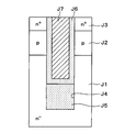
- FIG. 5A as shown in Figure 5B, the n-type drift layer J1, p-type base region J2 and the n + -type source region J3 are arranged structure, p-type base from the n + -type source region J3 Trench J4 is formed so as to penetrate region J2 and reach n type drift layer J1. Then, a bottom insulating film J5 is formed so as to remain at the bottom of the trench J4.
- the etch back amount is small, for example, as shown in FIG. 5A, the upper surface of the bottom insulating film J5 is positioned at a shallower position of the trench J4 than the bottom of the p-type base region J2. For this reason, when the gate insulating film J6 and the gate electrode J7 are formed on the bottom insulating film J5, the gate electrode J7 does not face the entire thickness direction of the p-type base region J2. Therefore, the channel region cannot be formed over the entire p-type base region J2 located on the side surface of the trench J4, and a vertical MOSFET having good characteristics cannot be obtained.
- the bottom insulating film J5 becomes thin, and electric field concentration occurs in the gate insulating film J6 formed on the bottom insulating film J5.
- the dielectric breakdown of the gate insulating film J6 may reduce the long-term reliability of the vertical MOSFET.
- a vertical MOSFET having a trench gate structure including a bottom insulating film requires a controllability of etch back when forming the bottom insulating film, and has a problem that a process window is narrow.
- a semiconductor device includes a drain region formed of a first or second conductivity type semiconductor, and a first conductivity type disposed on the drain region and having a lower impurity concentration than the drain region.
- a drift layer composed of a semiconductor, a base region disposed on the drift layer and composed of a second conductivity type semiconductor, and disposed on an upper layer portion of the base region and having a higher concentration than the drift layer.
- a trench gate structure including a bottom insulating film disposed on a bottom portion of the trench below the first gate insulating film; a source electrode electrically connected to the source region and the contact region; and the drain region. And a drain electrode disposed on the back surface side.
- the trench is disposed deeper than the base region from the surface of the source region.
- the first gate insulating film is made of an insulating material having a dielectric constant higher than that of the bottom insulating film.
- the first gate insulating film is made of an insulating material having a dielectric constant higher than that of the bottom insulating film.
- the electric field concentration in the first gate insulating film can be relaxed, and the dielectric breakdown of the first gate insulating film can be suppressed.
- the bottom insulating film may be somewhat thinned. For this reason, during the manufacturing process of the trench gate structure, when the insulating material constituting the bottom insulating film embedded in the trench is etched back, it can be designed to have excessive etch back.
- the bottom insulating film may be somewhat thin.
- the dielectric breakdown of the first gate insulating film can be suppressed. Accordingly, the bottom of the first gate electrode can be formed to a position deeper than the bottom of the base region, and the channel region can be formed over the entire base region on the side surface of the trench.
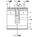
- FIG. 1 is a diagram illustrating a cross-sectional configuration of the SiC semiconductor device according to the first embodiment of the present disclosure.
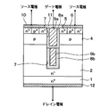
- FIG. 2 is a diagram illustrating a cross-sectional configuration of the SiC semiconductor device according to the second embodiment of the present disclosure
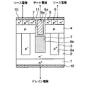
- FIG. 3 is a diagram illustrating a cross-sectional configuration of the SiC semiconductor device according to the third embodiment of the present disclosure.
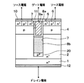
- FIG. 4 is a diagram illustrating a cross-sectional configuration of the SiC semiconductor device according to the fourth embodiment of the present disclosure.
- FIG. 5A is a cross-sectional view showing a change in the trench gate structure due to variations in etch back when forming a bottom insulating film in the trench; and FIG. 5B is a cross-sectional view showing a change in the trench gate structure due to variations in etch back when a bottom insulating film is formed in the trench.
- a first embodiment of the present disclosure will be described.
- a SiC semiconductor device in which the semiconductor device is formed of SiC will be described as an example.
- the semiconductor device may be formed of other semiconductor materials such as Si.
- FIG. 1 an SiC semiconductor device having a vertical MOSFET having an inverted trench gate structure according to the present embodiment will be described with reference to FIG.
- FIG. 1 only one cell of the vertical MOSFET is shown, but a plurality of cells having the same structure as the vertical MOSFET shown in FIG. 1 are arranged adjacent to each other.
- One cell here means from the center of the p + -type contact region 6 described later to the center of the p + -type contact region 6 located adjacent to the trench gate structure.
- an SiC single crystal having a thickness of about 300 ⁇ m is doped with an n-type impurity (such as phosphorus or nitrogen) at a high concentration, for example, an impurity concentration of 1 ⁇ 10 19 to 1 ⁇ 10 20 cm ⁇ 3.
- An SiC semiconductor device is formed using the n + type semiconductor substrate 1.
- an n type drift layer made of SiC having a thickness of about 5 to 15 ⁇ m doped with an n type impurity at an impurity concentration of 1 ⁇ 10 15 to 1 ⁇ 10 16 cm ⁇ 3 , for example. 2 is formed.
- a p-type base region 4 made of SiC is formed on the surface of the n-type drift layer 2.
- the p-type base region 4 is a layer constituting a channel region of the vertical MOSFET, and is formed on both sides of a trench 7 constituting a trench gate structure described later so as to be in contact with the side surface of the trench 7.
- the p-type base region 4 is doped with p-type impurities at an impurity concentration of, for example, 1 ⁇ 10 15 to 1 ⁇ 10 18 cm ⁇ 3 and has a thickness of about 0.7 to 1.8 ⁇ m.
- an n + -type source region 5 doped with an n-type impurity at a high concentration is formed so as to be in contact with the trench gate structure.
- the n + type source region 5 is formed by ion implantation into the p type base region 4 and the impurity concentration is about 1 ⁇ 10 21 cm ⁇ 3 and the thickness is about 0.3 ⁇ m.
- a p + -type contact region 6 doped with a high concentration of p-type impurities is formed on the opposite side of the trench 7 across the n + -type source region 5 in the surface layer portion of the p-type base region 4. .
- the p + -type contact region 6 is formed by ion implantation into the p-type base region 4 and the impurity concentration is about 1 ⁇ 10 21 cm ⁇ 3 and the thickness is about 0.3 ⁇ m. Forming.
- a trench 7 is formed which penetrates the p-type base region 4 and the n + -type source region 5 to reach the n-type drift layer 2 and has a bottom portion having a depth separated from the surface of the n + -type semiconductor substrate 1 by a predetermined distance. Has been. Therefore, the p-type base region 4 and the n + -type source region 5 are arranged so as to be in contact with the side surface of the trench 7.
- a trench gate structure is formed in the trench 7.
- the first gate electrode 9a is formed on the entrance side of the trench 7 in the trench 7 via the first gate insulating film 8a, and the bottom insulating film 8b is formed below this, that is, at the bottom of the trench 7. ing.
- the bottom insulating film 8b is formed at the bottom of the trench 7, and the first gate insulating film 8a is formed so as to cover the side surface of the trench 7 and the top surface of the bottom insulating film 8b.
- the trench 7 is filled up by disposing the first gate electrode 9a on the surface of the first gate insulating film 8a.
- the trench gate structure is constituted by the structure in which the first gate insulating film 8a, the first gate electrode 9a, and the bottom insulating film 8b are provided in the trench 7.
- the first gate insulating film 8a is made of an insulating material having a dielectric constant higher than that of the bottom insulating film 8b.
- the first gate insulating film 8a is made of silicon oxynitride, silicon nitride, aluminum oxide, aluminum nitride, hafnium oxide, hafnium nitride, titanium oxide, zirconium oxide, rare earth oxide (for example, lanthanum oxide, cerium oxide, yttrium oxide). Any one of these, a mixture of any two or more, or a stack of any two or more, and has a film thickness of, for example, about 50 to 200 nm.
- the first gate electrode 9 a is formed from the surface of the trench 7 to a position deeper than the bottom of the p-type base region 4.
- the first gate electrode 9a is made of Poly-Si doped with impurities, and a gate voltage can be applied by being connected to a gate wiring (not shown).
- a gate voltage can be applied by being connected to a gate wiring (not shown).
- a channel region can be formed on the side surface of the trench 7 in the p-type base region 4, that is, the entire region facing the first gate electrode 9a.
- the bottom of the first gate electrode 9a may be located deeper than the bottom of the p-type base region 4. For example, the depth is set to 0.8 to 2 ⁇ m.
- the bottom insulating film 8b provided at the bottom of the trench 7 is made of a material having a dielectric constant lower than that of the first gate insulating film 8a, such as a silicon oxide film (SiO 2 ).
- the thickness of the bottom insulating film 8b is arbitrary as long as the bottom insulating film 8b is formed within the thickness of the n-type drift layer 2, but in this embodiment, for example, the bottom insulating film 8b is about 0.8 to 2 ⁇ m. Has been.
- the trench gate structure is, for example, a strip with the vertical direction on the paper as the longitudinal direction, and a plurality of trench gate structures are arranged in stripes at equal intervals in the horizontal direction of the paper. As a result, the structure is provided with a plurality of cells.
- a source electrode 10 is formed on the surfaces of the n + type source region 5 and the p + type contact region 6.
- the source electrode 10 is composed of a plurality of metals (for example, Ni / Al). Specifically, the portion connected to n + type source region 5 is made of a metal capable of ohmic contact with n type SiC, and the portion connected to p type base region 4 via p + type contact region 6 is It is made of a metal capable of ohmic contact with p-type SiC.
- the source electrode 10 is electrically separated from a gate wiring (not shown) that is electrically connected to the first gate electrode 9a via the interlayer insulating film 11.
- the source electrode 10 is in electrical contact with the n + type source region 5 and the p + type contact region 6 through a contact hole formed in the interlayer insulating film 11.
- n + -type semiconductor substrate 1 On the back side of the n + -type semiconductor substrate 1 n + -type semiconductor substrate 1 and electrically connected to the drain electrode 12 are formed. With such a structure, an n-channel type inverted MOSFET having a trench gate structure is formed.
- the portion of the p-type base region 4 that is in contact with the side surface of the trench 7 becomes an inverted channel, and the source electrode 10 and the drain A current is passed between the electrodes 12.
- a high voltage eg, 1200 V
- SiC having an electric field breakdown strength close to 10 times that of a silicon device an electric field close to 10 times that of a silicon device is applied to the trench gate structure due to the influence of this voltage, and electric field concentration can occur.
- the first gate insulating film 8a is made of an insulating material having a high dielectric constant, the electric field concentration at the off time can be reduced. That is, when the first gate insulating film 8a is formed of an insulating material having a high dielectric constant, it is possible to suppress the entry of a high voltage into the first gate insulating film 8a as compared to a case where the first gate insulating film 8a is formed of an insulating material having a low dielectric constant. .
- the first gate insulating film 8a is made of an insulating material having a dielectric constant higher than that of the bottom insulating film 8b.
- the electric field concentration in the first gate insulating film 8a can be relaxed, and the dielectric breakdown of the first gate insulating film 8a can be suppressed.
- the bottom part insulating film 8b may be thinned a little. For this reason, during the manufacturing process of the trench gate structure, when the insulating material constituting the bottom insulating film 8b embedded in the trench 7 is etched back, it can be designed to have excessive etch back.
- the manufacturing process of the trench gate structure is performed as follows. First, after forming the trench 7 so as to penetrate the p-type base region 4 and the n + -type source region 5 and reach the n-type drift layer 2, the trench 7 is buried with an insulating material constituting the bottom insulating film 8b.
- the trench 7 is filled with an insulating material constituting the bottom insulating film 8b by CVD (chemical vapor deposition) or ALD (atomic layer deposition). Subsequently, the insulating material constituting the bottom insulating film 8b embedded in the trench 7 is etched back to form the bottom insulating film 8b.
- the first gate electrode 9a is disposed on the first gate insulating film 8a. In this way, a trench gate structure of a vertical MOSFET provided with a bottom insulating film is formed.
- the trench gate structure is formed by such a manufacturing process, when the insulating material constituting the bottom insulating film 8b embedded in the trench 7 is etched back, the top surface of the bottom insulating film 8b is surely formed of the p-type base region 4. Excessive etch back is performed so that it is located deeper than the bottom. In this case, there is a possibility that the bottom insulating film 8b is somewhat thin. However, even if the bottom insulating film 8b is somewhat thin, the first gate insulating film 8a is made of an insulating material having a high dielectric constant. The dielectric breakdown of the insulating film 8a can be suppressed.
- the bottom of the first gate electrode 9a can be formed to a position deeper than the bottom of the p-type base region 4, and a channel region can be formed in the entire region of the p-type base region 4 on the side surface of the trench 7. Can be.
- the bottom insulating film 8b is made of the same insulating material as the first gate insulating film 8a as in the conventional case, when the bottom insulating film 8b is formed thin, the parasitic capacitance Cgd increases and the switching speed decreases. I could invite you.
- the bottom insulating film 8b is made of an insulating material having a lower dielectric constant than the first gate insulating film. Therefore, even if the bottom insulating film 8b is thinned, the parasitic capacitance Cgd is reduced. it can. For this reason, it is also possible to suppress a decrease in switching speed.
- the trench gate structure is a double gate structure having an upper gate structure and a lower gate structure.
- an upper gate structure having a first gate insulating film 8a and a first gate electrode 9a is provided in the trench 7 on the upper stage side which is the entrance side of the trench 7.
- a lower gate structure having a bottom insulating film 8b and a second gate electrode 9b is provided on the lower stage side below the upper gate structure. That is, the bottom insulating film 8b constitutes the second gate insulating film, and the second gate electrode 9b is disposed in the bottom insulating film 8b.
- the second gate electrode 9b is made of Poly-Si doped with impurities, and is connected to the source electrode 10 in a cross section different from that shown in FIG.
- Such a structure forms a trench gate structure in which a double gate structure having an upper gate structure and a lower gate structure is formed in the trench 7.
- the first gate insulating film 8a is formed of an insulating material having a high dielectric constant and the second gate insulating film is formed as in the first embodiment.
- the bottom insulating film 8b can be made of an insulating material having a lower dielectric constant.
- a third embodiment of the present disclosure will be described.
- the present embodiment has a structure capable of further increasing the breakdown voltage compared to the first and second embodiments, and the other aspects are the same as those of the first and second embodiments, and therefore the first and second embodiments. Only different parts will be described.
- the structure of this embodiment is applied with respect to the structure of 1st Embodiment is demonstrated here, the same structure is applicable also to 2nd Embodiment.
- the p-type deep layer 3 is formed on both sides of the trench gate structure so as to be separated from the trench 7 by a predetermined distance.
- the p-type deep layer 3 is formed in a strip shape parallel to the trench 7, that is, in a strip shape with the vertical direction in FIG. 3 as the longitudinal direction, and a plurality of p-type deep layers 3 are arranged in a stripe shape.
- trenches 7 are arranged between the p-type deep layers 3.
- the n-type drift layer 2 is formed with a recessed portion (first recessed portion) 2a that is partially recessed, and a p-type impurity is formed in the recessed portion 2a.
- a p-type deep layer 3 is formed by embedding a p-type layer doped with.
- the p-type deep layer 3 has a higher p-type impurity concentration than the p-type base region 4, for example, about 1 ⁇ 10 17 to 1 ⁇ 10 19 cm ⁇ 3 .
- the SiC semiconductor device has a structure including the p-type deep layer 3. For this reason, the depletion layer at the PN junction between the p-type deep layer 3 and the n-type drift layer 2 greatly extends toward the n-type drift layer 2, and a high voltage due to the influence of the drain voltage is applied to the bottom insulating film 8b. It becomes difficult to enter.
- the electric field concentration in the first gate insulating film 8a particularly the electric field concentration at the bottom of the trench 7 in the first gate insulating film 8a is reduced. It becomes possible to do. Thereby, the dielectric breakdown of the first gate insulating film 8a is further suppressed, and a high breakdown voltage SiC semiconductor device is obtained.
- a fourth embodiment of the present disclosure will be described.
- This embodiment also has a structure capable of further increasing the breakdown voltage compared to the first and second embodiments, and the other aspects are the same as those of the first and second embodiments, and therefore the first and second embodiments. Only different parts will be described.
- the structure of this embodiment is applied with respect to the structure of 1st Embodiment is demonstrated here, the same structure is applicable also to 2nd Embodiment.
- a p-type bottom layer 20 is formed in the surface layer portion of the n-type drift layer 2 at the bottom of the trench gate structure.
- the p-type bottom layer 20 is formed in a strip shape having the entire length of the bottom portion of the trench 7, that is, the direction perpendicular to the paper surface of FIG.
- the p-type bottom layer 20 is formed by ion-implanting p-type impurities after forming the trenches 7 and covering portions other than the trenches 7 with a mask.
- the p-type bottom layer 20 has a p-type impurity concentration higher than that of the p-type base region 4, for example, about 1 ⁇ 10 17 to 1 ⁇ 10 19 cm ⁇ 3 .
- the SiC semiconductor device according to the present embodiment has a structure including the p-type bottom layer 20. For this reason, the depletion layer at the PN junction between the p-type bottom layer 20 and the n-type drift layer 2 greatly extends to the n-type drift layer 2 side, and a high voltage due to the influence of the drain voltage is applied to the bottom insulating film 8b. It becomes difficult to enter.
- the electric field concentration in the first gate insulating film 8a particularly the electric field concentration at the bottom of the trench 7 in the first gate insulating film 8a is reduced. It becomes possible to do. Thereby, the dielectric breakdown of the first gate insulating film 8a is further suppressed, and a high breakdown voltage SiC semiconductor device is obtained.
- the side surface of the trench 7 is perpendicular to the substrate or the bottom of the trench 7 is closer to the entrance side.
- the side surface is reversely tapered by increasing the width. This is because if the side surface of the trench 7 is inclined, ion implantation is also performed on the side surface, which may change the element characteristics of the vertical MOSFET.
- the layout of the p-type deep layer 3 described in the third embodiment is an example, and is not limited to being formed in parallel to the trench 7, but may be formed so as to intersect the trench 7, It may be formed in a shape or a mesh shape.
- the trench 7 is not limited to a stripe shape, but may be a dot shape or a mesh shape.
- a structure including both the p-type deep layer 3 described in the third embodiment and the p-type bottom layer 20 described in the fourth embodiment may be adopted.
- the SiC semiconductor device has been described as an example.
- the semiconductor device may be composed of other semiconductor materials such as Si.
- the n type drift layer 2 is formed on the n + type semiconductor substrate 1 constituting the drain region.
- the n-type drift layer 2 is composed of an n-type substrate, and n-type impurity ion implantation is performed on the back side of the n-type substrate, thereby forming a drain region composed of the n + -type layer. You may make it.
- the p-type deep layer 3 is formed deeper than the trench 7, but it is sufficient that the p-type deep layer 3 is formed deeper than at least the bottom of the first gate insulating film 8a. That is, since it is the first gate insulating film 8a that protects against breakdown in the p-type deep layer 3, it is only necessary to reduce the electric field in the first gate insulating film 8a. Therefore, the effect of electric field relaxation in the first gate insulating film 8a can be obtained by making at least the p-type deep layer 3 deeper than the bottom of the first gate insulating film 8a.
- an n-channel type MOSFET in which the first conductivity type is n-type and the second conductivity type is p-type has been described as an example.
- the present disclosure can be applied to a channel type MOSFET.
- a MOSFET having a trench gate structure has been described as an example, but the present disclosure can be applied to an IGBT having a similar trench gate structure.
- the IGBT only changes the conductivity type of the substrate 1 from the n-type to the p-type with respect to the above-described embodiments, and the other structures and manufacturing methods are the same as those of the above-described embodiments.
Landscapes
- Electrodes Of Semiconductors (AREA)
Abstract
半導体装置は、ドレイン領域(1)と、前記ドレイン領域よりも低不純物濃度の第1導電型半導体で構成されたドリフト層(2)と、第2導電型半導体で構成されたベース領域(4)と、高濃度の第1導電型半導体で構成されたソース領域(5)と、高濃度とされた第2導電型半導体で構成されたコンタクト領域(6)と、トレンチ(7)の入口側に配置され、前記ベース領域よりも深くまで配置された第1ゲート絶縁膜(8a)と第1ゲート電極(9a)とを有すると共に、底部絶縁膜(8b)を含むトレンチゲート構造と、前記ソース領域および前記コンタクト領域に電気的に接続されたソース電極(10)と、前記ドレイン領域の裏面側に配置されたドレイン電極(12)と、を備える。前記トレンチは、前記ベース領域よりも深くまで配置される。また、前記第1ゲート絶縁膜は、前記底部絶縁膜よりも高い誘電率の絶縁材料で構成されている。
Description
本出願は、2015年3月24日に出願された日本特許出願番号2015-61394号に基づくもので、ここにその記載内容を援用する。
本開示は、トレンチゲート構造を有する半導体装置に関し、特に、炭化珪素(以下、SiCという)にて構成される半導体装置に適用されて好適である。
従来より、大電流が流せるようにチャネル密度を高くした構造としてトレンチゲート構造の縦型MOSFETを有する半導体装置が知られている。このトレンチゲート構造において、ゲート電極が配置されるトレンチ内におけるゲート絶縁膜の下方、つまりトレンチの底部に厚くされた絶縁膜(以下、底部絶縁膜という)を配置した構造がある(例えば、特許文献1参照)。このような構造とすることで、底部絶縁膜によるシールド効果によって寄生容量Cgdの低減を図ることが可能となり、底部絶縁膜を形成していないMOSFETと比較して、高速スイッチングを実現することが可能となる。
上記のような底部絶縁膜を備える縦型MOSFETにおけるトレンチゲート構造は、例えば次のようにして形成される。まず、n型ドリフト層の上にp型ベース領域を成膜したのち、さらにp型ベース領域の表層部にイオン注入などによってn+型ソース領域を形成する。続いて、n+型ソース領域からp型ベース領域を貫通してn型ドリフト層に達するトレンチを形成したのち、トレンチ内を埋め込むように底部絶縁膜を構成するために、ゲート絶縁膜と同じ絶縁材料を堆積する。そして、トレンチ内を埋め込んだ絶縁材料をエッチバックして底部絶縁膜を構成する。その後、トレンチおよび底部絶縁膜の表面にゲート絶縁膜を成膜したのち、ゲート絶縁膜上にゲート電極を配置する。このようにして、底部絶縁膜を備えた縦型MOSFETのトレンチゲート構造が形成される。
このような工程によって底部絶縁膜を形成する場合、絶縁材料のエッチバック制御性がMOSFETの性能に大きく影響してくる。
具体的には、図5A、図5Bに示すように、n型ドリフト層J1、p型ベース領域J2およびn+型ソース領域J3が配置された構造において、n+型ソース領域J3からp型ベース領域J2を貫通してn型ドリフト層J1に達するようにトレンチJ4を形成する。そして、トレンチJ4の底部に残るように底部絶縁膜J5を形成する。
このとき、エッチバック量が少ないと、例えば、図5Aに示すように底部絶縁膜J5の上面がp型ベース領域J2の底部よりもトレンチJ4の浅い位置に位置してしまう。このため、底部絶縁膜J5の上にゲート絶縁膜J6およびゲート電極J7を形成したときに、ゲート電極J7がp型ベース領域J2の厚み方向全域に対向した状態にならない。したがって、チャネル領域をトレンチJ4の側面に位置するp型ベース領域J2の全域に形成することができず、良い特性の縦型MOSFETが得られなくなる。
逆に、エッチバック量が多いと、例えば、図5Bに示すように底部絶縁膜J5が薄くなってしまい、底部絶縁膜J5の上に形成されるゲート絶縁膜J6内での電界集中が発生し、ゲート絶縁膜J6の絶縁破壊が懸念される。このため、縦型MOSFETの長期信頼性を低下させる可能性がある。
このように、底部絶縁膜を備えるトレンチゲート構造の縦型MOSFETでは、底部絶縁膜を形成する際のエッチバックの制御性が求められ、プロセスウィンドウが狭いという問題がある。
本開示は、的確にチャネル領域が形成できるようにしつつ、絶縁耐圧を確保でき、さらに広いプロセスウィンドウが得られる構造の半導体装置を提供することを目的とする。
本開示の一態様に係る半導体装置は、第1または第2導電型半導体にて構成されたドレイン領域と、前記ドレイン領域の上に配置され、前記ドレイン領域よりも低不純物濃度の第1導電型半導体で構成されたドリフト層と、前記ドリフト層の上に配置され、第2導電型半導体で構成されたベース領域と、前記ベース領域の上層部に配置され、前記ドリフト層よりも高濃度の第1導電型半導体で構成されたソース領域と、前記ベース領域の上層部に配置され、前記ベース層よりも高濃度とされた第2導電型半導体で構成されたコンタクト領域と、トレンチ内における入口側に配置され、前記トレンチの入口から前記ベース領域よりも深くまで配置された第1ゲート絶縁膜と該第1ゲート絶縁膜上に配置された第1ゲート電極とを有すると共に、前記トレンチ内における前記第1ゲート絶縁膜の下となる底部に配置された底部絶縁膜を含むトレンチゲート構造と、前記ソース領域および前記コンタクト領域に電気的に接続されたソース電極と、前記ドレイン領域の裏面側に配置されたドレイン電極と、を備える。前記トレンチは、前記ソース領域の表面から前記ベース領域よりも深くまで配置される。また、前記第1ゲート絶縁膜は、前記底部絶縁膜よりも高い誘電率の絶縁材料で構成されている。
このように、第1ゲート絶縁膜を底部絶縁膜よりも誘電率の高い絶縁材料で構成している。これにより、第1ゲート絶縁膜内での電界集中を緩和でき、第1ゲート絶縁膜の絶縁破壊を抑制することが可能となる。そして、このように第1ゲート絶縁膜の絶縁破壊を抑制できることから、底部絶縁膜が多少薄くなっても良い。このため、トレンチゲート構造の製造工程中において、トレンチ内に埋め込まれた底部絶縁膜を構成する絶縁材料をエッチバックする際に、エッチバック過多となる設計とすることができる。
この場合、底部絶縁膜が多少薄くなる可能性があるが、上記のように、底部絶縁膜が多少薄くなっても第1ゲート絶縁膜の絶縁破壊を抑制できる。これにより、第1ゲート電極の底部がベース領域の底部よりも深い位置まで形成されるようにでき、トレンチの側面においてベース領域の全域にチャネル領域が形成されるようにできる。
したがって、的確にチャネル領域が形成できるようにしつつ、絶縁耐圧を確保でき、さらに広いプロセスウィンドウが得られる構造の半導体装置とすることが可能となる。
本開示についての上記目的およびその他の目的、特徴や利点は、添付の図面を参照しながら下記の詳細な記述により、より明確になる。その図面は、
図1は、本開示の第1実施形態にかかるSiC半導体装置の断面構成を示す図であり、
図2は、本開示の第2実施形態にかかるSiC半導体装置の断面構成を示す図であり、
図3は、本開示の第3実施形態にかかるSiC半導体装置の断面構成を示す図であり、
図4は、本開示の第4実施形態にかかるSiC半導体装置の断面構成を示す図であり、
図5Aは、トレンチ内に底部絶縁膜を形成する場合のエッチバックのバラツキに伴うトレンチゲート構造の変化を示した断面図であり、及び、
図5Bは、トレンチ内に底部絶縁膜を形成する場合のエッチバックのバラツキに伴うトレンチゲート構造の変化を示した断面図である。
以下、本開示の実施形態について図に基づいて説明する。なお、以下の各実施形態相互において、互いに同一もしくは均等である部分には、同一符号を付して説明を行う。
(第1実施形態)
本開示の第1実施形態について説明する。ここでは、半導体装置をSiCによって形成したSiC半導体装置を例に挙げて説明するが、Siなどの他の半導体材料によって半導体装置を構成しても良い。
本開示の第1実施形態について説明する。ここでは、半導体装置をSiCによって形成したSiC半導体装置を例に挙げて説明するが、Siなどの他の半導体材料によって半導体装置を構成しても良い。
まず、本実施形態にかかる反転型のトレンチゲート構造の縦型MOSFETを有するSiC半導体装置について、図1を参照して説明する。なお、図1では、縦型MOSFETの1セル分しか記載していないが、図1に示す縦型MOSFETと同様の構造のものが複数セル隣り合うように配置されている。ここでいう1セルとは、後述するp+型コンタクト領域6の中心からトレンチゲート構造を挟んで隣に位置するp+型コンタクト領域6の中心までのことを意味している。
図1に示すように、n型不純物(リンもしくは窒素など)が高濃度、例えば1×10¹⁹~1×1020cm-3の不純物濃度でドープされた厚さ300μm程度のSiC単結晶からなるn+型半導体基板1を用いてSiC半導体装置を形成している。このn+型半導体基板1の上に、n型不純物が例えば1×10¹⁵~1×1016cm-3の不純物濃度でドープされた厚さが5~15μm程度のSiCからなるn型ドリフト層2が形成されている。
また、n型ドリフト層2の表面上に、SiCからなるp型ベース領域4が形成されている。p型ベース領域4は、縦型MOSFETのチャネル領域を構成する層であり、後述するトレンチゲート構造を構成するトレンチ7の両側において、トレンチ7の側面に接するように形成されている。p型ベース領域4は、p型不純物が例えば1×10¹⁵~1×1018cm-3の不純物濃度でドープされ、厚さが0.7~1.8μm程度で構成されている。
p型ベース領域4の表層部のうちのトレンチ7側には、トレンチゲート構造に接するようにn型不純物が高濃度にドープされたn+型ソース領域5が形成されている。本実施形態の場合、例えばn+型ソース領域5をp型ベース領域4へのイオン注入などによって形成しており、不純物濃度が1×1021cm-3程度、厚さが0.3μm程度で形成している。また、p型ベース領域4の表層部のうちn+型ソース領域5を挟んでトレンチ7と反対側には、p型不純物が高濃度にドープされたp+型コンタクト領域6が形成されている。本実施形態の場合、例えばp+型コンタクト領域6をp型ベース領域4へのイオン注入などによって形成しており、不純物濃度が1×1021cm-3程度、厚さが0.3μm程度で形成している。
さらに、p型ベース領域4およびn+型ソース領域5を貫通してn型ドリフト層2に達し、かつ、底部がn+型半導体基板1の表面から所定距離離れる深さとされたトレンチ7が形成されている。このため、トレンチ7の側面と接するようにp型ベース領域4およびn+型ソース領域5が配置された状態になっている。
そして、このトレンチ7内にトレンチゲート構造が構成されている。具体的には、トレンチ7内におけるトレンチ7の入口側には第1ゲート絶縁膜8aを介して第1ゲート電極9aが形成され、この下、つまりトレンチ7の底部に底部絶縁膜8bが形成されている。換言すれば、トレンチ7の底部に底部絶縁膜8bが形成され、トレンチ7の側面および底部絶縁膜8bの上面を覆うように第1ゲート絶縁膜8aが形成されている。そして、第1ゲート絶縁膜8aの表面に第1ゲート電極9aが配置されることで、トレンチ7内が埋め尽くされている。このように、トレンチ7内に第1ゲート絶縁膜8aや第1ゲート電極9aおよび底部絶縁膜8bを備えた構造により、トレンチゲート構造が構成されている。
第1ゲート絶縁膜8aは、底部絶縁膜8bよりも高い誘電率の絶縁材料によって構成されている。例えば、第1ゲート絶縁膜8aは、酸窒化珪素、窒化珪素、酸化アルミニウム、窒化アルミニウム、酸化ハフニウム、窒化ハフニウム、酸化チタニウム、酸化ジルコニウム、希土類酸化物(例えば、酸化ランタン、酸化セリウム、酸化イットリウム)のいずれか1つ、もしくはいずれか2つ以上の混合、もしくはいずれか2つ以上の積層によって形成され、例えば50~200nm程度の膜厚とされている。第1ゲート電極9aは、トレンチ7の表面からp型ベース領域4の底部よりも深い位置まで形成されている。第1ゲート電極9aは、不純物がドープされたPoly-Siにて構成されており、図示しないゲート配線に接続されることでゲート電圧が印加可能とされている。これにより、ゲート電圧印加時には、p型ベース領域4のうちトレンチ7の側面、つまり第1ゲート電極9aと対向する部分の全域にチャネル領域が形成可能とされている。第1ゲート絶縁膜8aおよび第1ゲート電極9aの全体を含めた部分の深さについては、第1ゲート電極9aの底部がp型ベース領域4の底部よりも深い位置となっていれば良いが、例えば0.8~2μmの深さに設定してある。
トレンチ7の底部に備えられる底部絶縁膜8bは、第1ゲート絶縁膜8aよりも低い誘電率の材料、例えばシリコン酸化膜(SiO2)などによって構成されている。底部絶縁膜8bの厚みについては、底部絶縁膜8bがn型ドリフト層2の厚み内に形成されていれば任意であるが、本実施形態では例えば底部絶縁膜8bは0.8~2μm程度とされている。
なお、図1では示されていないが、トレンチゲート構造は、例えば紙面垂直方向を長手方向とした短冊状とされており、複数本のトレンチゲート構造が紙面左右方向に等間隔にストライプ状に並べられることで複数セルが備えられた構造とされている。
また、n+型ソース領域5およびp+型コンタクト領域6の表面には、ソース電極10が形成されている。ソース電極10は、複数の金属(例えばNi/Al等)にて構成されている。具体的には、n+型ソース領域5に接続される部分はn型SiCとオーミック接触可能な金属で構成され、p+型コンタクト領域6を介してp型ベース領域4に接続される部分はp型SiCとオーミック接触可能な金属で構成されている。なお、ソース電極10は、層間絶縁膜11を介して、第1ゲート電極9aに電気的に接続される図示しないゲート配線と電気的に分離されている。そして、層間絶縁膜11に形成されたコンタクトホールを通じて、ソース電極10はn+型ソース領域5およびp+型コンタクト領域6と電気的に接触させられている。
さらに、n+型半導体基板1の裏面側にはn+型半導体基板1と電気的に接続されたドレイン電極12が形成されている。このような構造により、nチャネルタイプの反転型のトレンチゲート構造の縦型MOSFETが構成されている。
このように構成された縦型MOSFETは、第1ゲート電極9aに対してゲート電圧を印加すると、p型ベース領域4のうちトレンチ7の側面に接する部分が反転型チャネルとなり、ソース電極10とドレイン電極12との間に電流を流す。
一方、ゲート電圧を印加しない場合はドレイン電圧として高電圧(例えば1200V)が印加される。シリコンデバイスの10倍近い電界破壊強度を有するSiCでは、この電圧の影響によりトレンチゲート構造にもシリコンデバイスの10倍近い電界がかかり、電界集中が発生し得る。
しかしながら、本実施形態では、第1ゲート絶縁膜8aを誘電率の高い絶縁材料によって構成していることから、オフ時の電界集中を緩和できる。すなわち、誘電率の高い絶縁材料によって第1ゲート絶縁膜8aを構成すると、誘電率の低い絶縁材料で構成する場合と比較して、第1ゲート絶縁膜8a内への高電圧の入り込みを抑制できる。これにより、上側の第1ゲート絶縁膜8aへの電界の入り込みが抑制され、第1ゲート絶縁膜8a内における等電位線の間隔が広がって、第1ゲート絶縁膜8a内、特にトレンチ7のコーナー部の位置での電界集中が緩和される。したがって、第1ゲート電極9aとドレインとの間の絶縁を図るべき第1ゲート絶縁膜8aの絶縁破壊を抑制することが可能となる。
このように、第1ゲート絶縁膜8aを底部絶縁膜8bよりも誘電率の高い絶縁材料で構成している。これにより、第1ゲート絶縁膜8a内での電界集中を緩和でき、第1ゲート絶縁膜8aの絶縁破壊を抑制することが可能となる。そして、このように第1ゲート絶縁膜8aの絶縁破壊を抑制できることから、底部絶縁膜8bが多少薄くなっても良い。このため、トレンチゲート構造の製造工程中において、トレンチ7内に埋め込まれた底部絶縁膜8bを構成する絶縁材料をエッチバックする際に、エッチバック過多となる設計とすることができる。
具体的には、トレンチゲート構造の製造工程は次のようにして行われる。まず、p型ベース領域4およびn+型ソース領域5を貫通してn型ドリフト層2に達するようにトレンチ7を形成したのち、底部絶縁膜8bを構成する絶縁材料でトレンチ7を埋め込む。例えば、CVD(chemical vapor deposition)またはALD(atomic layer deposition)等によって底部絶縁膜8bを構成する絶縁材料でトレンチ7内を埋め込んでいる。続いて、トレンチ7に埋め込まれた底部絶縁膜8bを構成する絶縁材料をエッチバックし、底部絶縁膜8bを形成する。その後、トレンチ7および底部絶縁膜8bの表面にCVDやALD等によって第1ゲート絶縁膜8aを成膜したのち、第1ゲート絶縁膜8a上に第1ゲート電極9aを配置する。このようにして、底部絶縁膜を備えた縦型MOSFETのトレンチゲート構造が形成される。
このような製造工程によってトレンチゲート構造を形成にあたり、トレンチ7に埋め込まれた底部絶縁膜8bを構成する絶縁材料をエッチバックする際に、底部絶縁膜8bの上面が確実にp型ベース領域4の底部よりも深くに位置するようにエッチバックを多めに行う。この場合、底部絶縁膜8bが多少薄くなる可能性があるが、底部絶縁膜8bが多少薄くなっても第1ゲート絶縁膜8aを誘電率の高い絶縁材料で構成しているため、第1ゲート絶縁膜8aの絶縁破壊を抑制できる。これにより、第1ゲート電極9aの底部がp型ベース領域4の底部よりも深い位置まで形成されるようにでき、トレンチ7の側面においてp型ベース領域4の全域にチャネル領域が形成されるようにできる。
したがって、的確にチャネル領域が形成できるようにしつつ、絶縁耐圧を確保でき、さらに広いプロセスウィンドウが得られる構造の半導体装置とすることが可能となる。
また、底部絶縁膜8bを従来と同様に、第1ゲート絶縁膜8aと同じ絶縁材料で構成すると、底部絶縁膜8bが薄く形成された場合に、寄生容量Cgdが大きくなってスイッチング速度の低下を招きかねない。しかしながら、本実施形態の場合、底部絶縁膜8bを第1ゲート絶縁膜よりも誘電率の低い絶縁材料で構成していることから、仮に底部絶縁膜8bが薄くなったとしても寄生容量Cgdを小さくできる。このため、スイッチング速度の低下を抑制することも可能となる。
(第2実施形態)
本開示の第2実施形態について説明する。本実施形態は、第1実施形態に対してトレンチゲート構造を変更したものであり、その他については第1実施形態と同様であるため、第1実施形態と異なる部分についてのみ説明する。
本開示の第2実施形態について説明する。本実施形態は、第1実施形態に対してトレンチゲート構造を変更したものであり、その他については第1実施形態と同様であるため、第1実施形態と異なる部分についてのみ説明する。
図2に示すように、本実施形態では、トレンチゲート構造を上段側ゲート構造と下段側ゲート構造とを備えたダブルゲート構造としている。具体的には、トレンチ7内において、トレンチ7の入口側となる上段側に、第1ゲート絶縁膜8aと第1ゲート電極9aを有する上段側ゲート構造が備えられている。また、その上段側ゲート構造の下となる下段側に、底部絶縁膜8bと第2ゲート電極9bを有する下段側ゲート構造が備えられている。つまり、底部絶縁膜8bによって第2ゲート絶縁膜を構成し、底部絶縁膜8b内に第2ゲート電極9bを配置している。第2ゲート電極9bは、不純物がドープされたPoly-Siにて構成されており、図2とは別断面においてソース電極10に接続されてソース電位とされる。
このような構造により、トレンチ7内において上段側ゲート構造および下段側ゲート構造のダブルゲート構造が形成されたトレンチゲート構造が構成されている。
このように、トレンチゲート構造がダブルゲート構造とされる場合においても、第1実施形態と同様に、第1ゲート絶縁膜8aを誘電率の高い絶縁材料で構成し、第2ゲート絶縁膜を構成する底部絶縁膜8bをそれよりも誘電率の低い絶縁材料で構成できる。このような構成とすることで、第1実施形態と同様の効果を得ることが可能とになる。また、第2ゲート電極9bをソース電位にすることで、より寄生容量Cgdの低減やトレンチゲート底部での電界緩和を図ることが可能となり、さらにスイッチング速度および絶縁耐圧の向上を図ることが可能となる。
(第3実施形態)
本開示の第3実施形態について説明する。本実施形態は、第1、第2実施形態に対して更に高耐圧化できる構造としたものであり、その他については第1、第2実施形態と同様であるため、第1、第2実施形態と異なる部分についてのみ説明する。なお、ここでは第1実施形態の構造に対して本実施形態の構造を適用する場合について説明するが、第2実施形態についても同様の構造を適用できる。
本開示の第3実施形態について説明する。本実施形態は、第1、第2実施形態に対して更に高耐圧化できる構造としたものであり、その他については第1、第2実施形態と同様であるため、第1、第2実施形態と異なる部分についてのみ説明する。なお、ここでは第1実施形態の構造に対して本実施形態の構造を適用する場合について説明するが、第2実施形態についても同様の構造を適用できる。
図3に示すように、本実施形態のSiC半導体装置では、トレンチゲート構造の両側において、トレンチ7から所定距離離れるようにp型ディープ層3が形成されている。本実施形態の場合、p型ディープ層3は、トレンチ7と平行に、つまり図3の紙面垂直方向を長手方向とした短冊状とされ、複数本のp型ディープ層3がストライプ状に並べられ、各p型ディープ層3の間にトレンチ7が配置されたレイアウトとされている。具体的には、トレンチ7が形成される位置の両側において、n型ドリフト層2には部分的に凹まされた凹部(第1凹部)2aが形成されており、この凹部2a内にp型不純物がドープされたp型層が埋め込まれることによってp型ディープ層3が形成されている。p型ディープ層3は、p型ベース領域4よりもp型不純物濃度が高濃度とされており、例えば1×10¹⁷~1×1019cm-3程度とされている。
このように、本実施形態にかかるSiC半導体装置では、p型ディープ層3を備えた構造としている。このため、p型ディープ層3とn型ドリフト層2とのPN接合部での空乏層がn型ドリフト層2側に大きく伸びることになり、ドレイン電圧の影響による高電圧が底部絶縁膜8bに入り込み難くなる。
したがって、第1ゲート絶縁膜8aへは更に高電圧が入り込み難くなり、第1ゲート絶縁膜8a内での電界集中、特に第1ゲート絶縁膜8aのうちのトレンチ7の底部での電界集中を緩和することが可能となる。これにより、より第1ゲート絶縁膜8aの絶縁破壊が抑制され、高耐圧のSiC半導体装置となる。
(第4実施形態)
本開示の第4実施形態について説明する。本実施形態も、第1、第2実施形態に対して更に高耐圧化できる構造としたものであり、その他については第1、第2実施形態と同様であるため、第1、第2実施形態と異なる部分についてのみ説明する。なお、ここでは第1実施形態の構造に対して本実施形態の構造を適用する場合について説明するが、第2実施形態についても同様の構造を適用できる。
本開示の第4実施形態について説明する。本実施形態も、第1、第2実施形態に対して更に高耐圧化できる構造としたものであり、その他については第1、第2実施形態と同様であるため、第1、第2実施形態と異なる部分についてのみ説明する。なお、ここでは第1実施形態の構造に対して本実施形態の構造を適用する場合について説明するが、第2実施形態についても同様の構造を適用できる。
図4に示すように、本実施形態のSiC半導体装置では、トレンチゲート構造の底部におけるn型ドリフト層2の表層部に、p型ボトム層20が形成されている。本実施形態の場合、p型ボトム層20は、トレンチ7の底部の全域、つまり図4の紙面垂直方向を長手方向とした短冊状に形成されている。例えば、p型ボトム層20は、トレンチ7を形成したのち、トレンチ7以外の部分をマスクで覆った状態でp型不純物をイオン注入することで形成される。p型ボトム層20は、p型ベース領域4よりもp型不純物濃度が高濃度とされており、例えば1×10¹⁷~1×1019cm-3程度とされている。
このように、本実施形態にかかるSiC半導体装置では、p型ボトム層20を備えた構造としている。このため、p型ボトム層20とn型ドリフト層2とのPN接合部での空乏層がn型ドリフト層2側に大きく伸びることになり、ドレイン電圧の影響による高電圧が底部絶縁膜8bに入り込み難くなる。
したがって、第1ゲート絶縁膜8aへは更に高電圧が入り込み難くなり、第1ゲート絶縁膜8a内での電界集中、特に第1ゲート絶縁膜8aのうちのトレンチ7の底部での電界集中を緩和することが可能となる。これにより、より第1ゲート絶縁膜8aの絶縁破壊が抑制され、高耐圧のSiC半導体装置となる。
なお、本実施形態のようなトレンチ7の底部に形成されるp型ボトム層20をイオン注入によって形成する場合、トレンチ7の側面が基板に対して垂直もしくはトレンチ7の底部の方が入口側よりも幅広となることで側面が逆テーパ状とされるのが好ましい。これは、トレンチ7の側面が傾斜していると、その側面にもイオン注入が行われることになり、縦型MOSFETの素子特性を変動させる可能性があるためである。
(他の実施形態)
本開示は上記した実施形態に限定されるものではなく、本開示に記載された技術の範囲において適宜変更が可能である。
本開示は上記した実施形態に限定されるものではなく、本開示に記載された技術の範囲において適宜変更が可能である。
例えば、第3実施形態で説明したp型ディープ層3のレイアウトは一例であり、トレンチ7に対して平行に形成されている場合に限らず、トレンチ7と交差するように形成されていたり、ドット状や網目状に形成されていても良い。また、トレンチ7についてもストライプ状に限らず、ドット状とされていたり、網目状とされていても良い。
また、第3実施形態で説明したp型ディープ層3と第4実施形態で説明したp型ボトム層20の両方を備えた構造としても良い。
また、上記実施形態では、SiC半導体装置を例に挙げて説明したが、Siなどの他の半導体材料によって半導体装置を構成しても良い。上記各実施形態で説明したSiC半導体装置の場合、ドレイン領域を構成するn+型半導体基板1の上にn型ドリフト層2を成膜するようにしている。これに対して、n型ドリフト層2をn型基板で構成し、n型基板の裏面側にn型不純物イオン注入を行うことなどにより、n+型層にて構成されるドレイン領域が形成されるようにしても良い。
また、上記第3実施形態では、p型ディープ層3をトレンチ7よりも深くまで形成しているが、少なくとも第1ゲート絶縁膜8aの底部よりも深くまで形成されていれば良い。すなわち、p型ディープ層3にて絶縁破壊から保護するのは第1ゲート絶縁膜8aであることから、第1ゲート絶縁膜8a内での電界緩和が図れれば良い。したがって、少なくともp型ディープ層3を第1ゲート絶縁膜8aの底部よりも深くすることで、第1ゲート絶縁膜8a内での電界緩和の効果を得ることができる。
また、上記各実施形態では、第1導電型をn型、第2導電型をp型としたnチャネルタイプのMOSFETを例に挙げて説明したが、各構成要素の導電型を反転させたpチャネルタイプのMOSFETに対しても本開示を適用することができる。また、上記説明では、トレンチゲート構造のMOSFETを例に挙げて説明したが、同様のトレンチゲート構造のIGBTに対しても本開示を適用することができる。IGBTは、上記各実施形態に対して基板1の導電型をn型からp型に変更するだけであり、その他の構造や製造方法に関しては上記各実施形態と同様である。
本開示は、実施例に準拠して記述されたが、本開示は当該実施例や構造に限定されるものではないと理解される。本開示は、様々な変形例や均等範囲内の変形をも包含する。加えて、様々な組み合わせや形態、さらには、それらに一要素のみ、それ以上、あるいはそれ以下、を含む他の組み合わせや形態をも、本開示の範疇や思想範囲に入るものである。
Claims (10)
- 第1または第2導電型半導体にて構成されたドレイン領域(1)と、
前記ドレイン領域の上に配置され、前記ドレイン領域よりも低不純物濃度の第1導電型半導体で構成されたドリフト層(2)と、
前記ドリフト層の上に配置され、第2導電型半導体で構成されたベース領域(4)と、
前記ベース領域の上層部に配置され、前記ドリフト層よりも高濃度の第1導電型半導体で構成されたソース領域(5)と、
前記ベース領域の上層部に配置され、前記ベース層よりも高濃度とされた第2導電型半導体で構成されたコンタクト領域(6)と、
トレンチ(7)内における入口側に配置され、前記トレンチの入口から前記ベース領域よりも深くまで配置された第1ゲート絶縁膜(8a)と該第1ゲート絶縁膜上に配置された第1ゲート電極(9a)とを有すると共に、前記トレンチ内における前記第1ゲート絶縁膜の下となる底部に配置された底部絶縁膜(8b)を含むトレンチゲート構造と、
前記ソース領域および前記コンタクト領域に電気的に接続されたソース電極(10)と、
前記ドレイン領域の裏面側に配置されたドレイン電極(12)と、を備え、
前記トレンチは、前記ソース領域の表面から前記ベース領域よりも深くまで配置され、
前記第1ゲート絶縁膜は、前記底部絶縁膜よりも高い誘電率の絶縁材料で構成されている半導体装置。 - 前記第1ゲート絶縁膜および前記第1ゲート電極は、前記トレンチ内おける上段側に配置された上段側ゲート構造を構成しており、
前記トレンチ内における前記上段側ゲート構造の下となる下段側に、前記底部絶縁膜によって構成される第2ゲート絶縁膜と、該第2ゲート絶縁膜上に配置された第2ゲート電極(9b)とを有する下段側ゲート構造が構成され、
前記上段側ゲート構造と前記下段側ゲート構造によってダブルゲート構造によるトレンチゲート構造が構成されている請求項1に記載の半導体装置。 - 前記第2ゲート電極は、前記ソース電極と接続されてソース電位とされている請求項2に記載の半導体装置。
- 前記底部絶縁膜はシリコン酸化膜によって構成されており、
前記第1ゲート絶縁膜はシリコン酸化膜よりも誘電率の高い絶縁材料によって構成されている請求項1ないし3のいずれか1つに記載の半導体装置。 - 前記第1ゲート絶縁膜は酸窒化珪素、窒化珪素、酸化アルミニウム、窒化アルミニウム、酸化ハフニウム、窒化ハフニウム、酸化チタニウム、酸化ジルコニウム、希土類酸化物のいずれか1つによって構成されている請求項4に記載の半導体装置。
- 前記第1ゲート絶縁膜は酸窒化珪素、窒化珪素、酸化アルミニウム、窒化アルミニウム、酸化ハフニウム、窒化ハフニウム、酸化チタニウム、酸化ジルコニウム、希土類酸化物のいずれか2つ以上の混合材料によって構成されている請求項4に記載の半導体装置。
- 前記第1ゲート絶縁膜は酸窒化珪素、窒化珪素、酸化アルミニウム、窒化アルミニウム、酸化ハフニウム、窒化ハフニウム、酸化チタニウム、酸化ジルコニウム、希土類酸化物のいずれか2つ以上の積層によって構成されている請求項4に記載の半導体装置。
- 前記ベース領域よりも下方に位置する前記ドリフト層内において、前記第1ゲート絶縁膜の底部よりも深くまで配置され、前記ベース領域よりも第2導電型の不純物濃度が高濃度とされた第2導電型のディープ層(3)を有している請求項1ないし7のいずれか1つに記載の半導体装置。
- 前記トレンチの底部における前記ドリフト層内において、前記ベース領域よりも第2導電型の不純物濃度が高濃度とされた第2導電型のボトム層(20)を有している請求項1ないし8のいずれか1つに記載の半導体装置。
- 請求項1ないし9のいずれか1つに記載の半導体装置を構成する半導体が炭化珪素によって構成されている炭化珪素半導体装置。
Priority Applications (2)
| Application Number | Priority Date | Filing Date | Title |
|---|---|---|---|
| US15/560,662 US10290707B2 (en) | 2015-03-24 | 2016-03-10 | Semiconductor device |
| CN201680017258.XA CN107431093A (zh) | 2015-03-24 | 2016-03-10 | 半导体装置 |
Applications Claiming Priority (2)
| Application Number | Priority Date | Filing Date | Title |
|---|---|---|---|
| JP2015-061394 | 2015-03-24 | ||
| JP2015061394A JP2016181617A (ja) | 2015-03-24 | 2015-03-24 | 半導体装置 |
Publications (1)
| Publication Number | Publication Date |
|---|---|
| WO2016152059A1 true WO2016152059A1 (ja) | 2016-09-29 |
Family
ID=56977315
Family Applications (1)
| Application Number | Title | Priority Date | Filing Date |
|---|---|---|---|
| PCT/JP2016/001322 Ceased WO2016152059A1 (ja) | 2015-03-24 | 2016-03-10 | 半導体装置 |
Country Status (4)
| Country | Link |
|---|---|
| US (1) | US10290707B2 (ja) |
| JP (1) | JP2016181617A (ja) |
| CN (1) | CN107431093A (ja) |
| WO (1) | WO2016152059A1 (ja) |
Cited By (1)
| Publication number | Priority date | Publication date | Assignee | Title |
|---|---|---|---|---|
| CN109524399A (zh) * | 2017-09-18 | 2019-03-26 | 三星电子株式会社 | 半导体存储器件及其制造方法 |
Families Citing this family (9)
| Publication number | Priority date | Publication date | Assignee | Title |
|---|---|---|---|---|
| JP7116409B2 (ja) * | 2017-02-27 | 2022-08-10 | 株式会社タムラ製作所 | トレンチmos型ショットキーダイオード |
| JP6717242B2 (ja) * | 2017-03-13 | 2020-07-01 | 豊田合成株式会社 | 半導体装置 |
| DE102018104581B4 (de) * | 2017-03-24 | 2021-11-04 | Infineon Technologies Ag | Siliziumcarbid-Halbleitervorrichtung und Herstellungsverfahren |
| JP2020009898A (ja) * | 2018-07-06 | 2020-01-16 | トヨタ自動車株式会社 | 半導体装置 |
| CN111370475A (zh) | 2018-12-25 | 2020-07-03 | 广东美的白色家电技术创新中心有限公司 | 沟槽栅igbt及装置 |
| JP7180402B2 (ja) * | 2019-01-21 | 2022-11-30 | 株式会社デンソー | 半導体装置 |
| JP7199270B2 (ja) | 2019-03-20 | 2023-01-05 | 株式会社東芝 | 半導体装置及び半導体回路 |
| US20210050420A1 (en) * | 2019-08-13 | 2021-02-18 | Semiconductor Components Industries, Llc | Silicon carbide trench power device |
| JP7721470B2 (ja) | 2022-03-22 | 2025-08-13 | 株式会社東芝 | 半導体装置 |
Citations (5)
| Publication number | Priority date | Publication date | Assignee | Title |
|---|---|---|---|---|
| JP2002319583A (ja) * | 2001-02-02 | 2002-10-31 | Samsung Electronics Co Ltd | 半導体素子の誘電体膜及びその製造方法 |
| JP2004039813A (ja) * | 2002-07-02 | 2004-02-05 | Fujitsu Ltd | 半導体装置および非晶質高誘電体膜の堆積方法 |
| JP2010129973A (ja) * | 2008-12-01 | 2010-06-10 | Toyota Motor Corp | 半導体装置 |
| JP2011108701A (ja) * | 2009-11-13 | 2011-06-02 | Renesas Electronics Corp | 半導体装置の製造方法 |
| JP2011159763A (ja) * | 2010-01-29 | 2011-08-18 | Toshiba Corp | 電力用半導体装置 |
Family Cites Families (16)
| Publication number | Priority date | Publication date | Assignee | Title |
|---|---|---|---|---|
| US6849898B2 (en) | 2001-08-10 | 2005-02-01 | Siliconix Incorporated | Trench MIS device with active trench corners and thick bottom oxide |
| US7290037B2 (en) * | 2002-08-22 | 2007-10-30 | Clark Todd A | Scalable wireless remote control and monitoring system with automatic registration and automatic time synchronization |
| US7638841B2 (en) | 2003-05-20 | 2009-12-29 | Fairchild Semiconductor Corporation | Power semiconductor devices and methods of manufacture |
| JP4903055B2 (ja) | 2003-12-30 | 2012-03-21 | フェアチャイルド・セミコンダクター・コーポレーション | パワー半導体デバイスおよびその製造方法 |
| JP4955222B2 (ja) | 2005-05-20 | 2012-06-20 | ルネサスエレクトロニクス株式会社 | 半導体装置の製造方法 |
| US8653589B2 (en) * | 2009-04-15 | 2014-02-18 | Force Mos Technology Co., Ltd. | Low Qgd trench MOSFET integrated with schottky rectifier |
| JP5717661B2 (ja) * | 2011-03-10 | 2015-05-13 | 株式会社東芝 | 半導体装置とその製造方法 |
| JP5878331B2 (ja) | 2011-10-18 | 2016-03-08 | トヨタ自動車株式会社 | 半導体装置及びその製造方法 |
| JP5812029B2 (ja) * | 2012-06-13 | 2015-11-11 | 株式会社デンソー | 炭化珪素半導体装置およびその製造方法 |
| JP2014146666A (ja) * | 2013-01-28 | 2014-08-14 | Toshiba Corp | 半導体装置 |
| JP2015207588A (ja) * | 2014-04-17 | 2015-11-19 | ローム株式会社 | 半導体装置 |
| WO2016052203A1 (ja) * | 2014-09-30 | 2016-04-07 | 三菱電機株式会社 | 半導体装置 |
| JP2016181618A (ja) * | 2015-03-24 | 2016-10-13 | 株式会社デンソー | 半導体装置 |
| JP6409681B2 (ja) * | 2015-05-29 | 2018-10-24 | 株式会社デンソー | 半導体装置およびその製造方法 |
| JP6750300B2 (ja) * | 2016-05-16 | 2020-09-02 | 富士電機株式会社 | 半導体装置および半導体装置の製造方法 |
| JP7182850B2 (ja) * | 2016-11-16 | 2022-12-05 | 富士電機株式会社 | 炭化珪素半導体装置および炭化珪素半導体装置の製造方法 |
-
2015
- 2015-03-24 JP JP2015061394A patent/JP2016181617A/ja active Pending
-
2016
- 2016-03-10 CN CN201680017258.XA patent/CN107431093A/zh active Pending
- 2016-03-10 US US15/560,662 patent/US10290707B2/en not_active Expired - Fee Related
- 2016-03-10 WO PCT/JP2016/001322 patent/WO2016152059A1/ja not_active Ceased
Patent Citations (5)
| Publication number | Priority date | Publication date | Assignee | Title |
|---|---|---|---|---|
| JP2002319583A (ja) * | 2001-02-02 | 2002-10-31 | Samsung Electronics Co Ltd | 半導体素子の誘電体膜及びその製造方法 |
| JP2004039813A (ja) * | 2002-07-02 | 2004-02-05 | Fujitsu Ltd | 半導体装置および非晶質高誘電体膜の堆積方法 |
| JP2010129973A (ja) * | 2008-12-01 | 2010-06-10 | Toyota Motor Corp | 半導体装置 |
| JP2011108701A (ja) * | 2009-11-13 | 2011-06-02 | Renesas Electronics Corp | 半導体装置の製造方法 |
| JP2011159763A (ja) * | 2010-01-29 | 2011-08-18 | Toshiba Corp | 電力用半導体装置 |
Cited By (2)
| Publication number | Priority date | Publication date | Assignee | Title |
|---|---|---|---|---|
| CN109524399A (zh) * | 2017-09-18 | 2019-03-26 | 三星电子株式会社 | 半导体存储器件及其制造方法 |
| CN109524399B (zh) * | 2017-09-18 | 2024-03-05 | 三星电子株式会社 | 半导体存储器件及其制造方法 |
Also Published As
| Publication number | Publication date |
|---|---|
| JP2016181617A (ja) | 2016-10-13 |
| US10290707B2 (en) | 2019-05-14 |
| US20180097061A1 (en) | 2018-04-05 |
| CN107431093A (zh) | 2017-12-01 |
Similar Documents
| Publication | Publication Date | Title |
|---|---|---|
| WO2016152058A1 (ja) | 半導体装置 | |
| WO2016152059A1 (ja) | 半導体装置 | |
| CN105264667B (zh) | 碳化硅半导体装置及其制造方法 | |
| TWI649872B (zh) | 半導體裝置 | |
| US9245995B2 (en) | Semiconductor device having power metal-oxide-semiconductor transistor | |
| US8680608B2 (en) | Power semiconductor device with a low on resistence | |
| US10903202B2 (en) | Semiconductor device | |
| US20200295150A1 (en) | Semiconductor device | |
| US20120241761A1 (en) | Semiconductor device and method for manufacturing same | |
| CN105593996A (zh) | 碳化硅半导体装置 | |
| CN116918072A (zh) | 场效应晶体管及其制造方法 | |
| US20140209999A1 (en) | Semiconductor device | |
| JP5700027B2 (ja) | 半導体装置 | |
| JP2013125827A (ja) | 半導体装置およびその製造方法 | |
| CN102403356A (zh) | 半导体装置 | |
| CN102694014A (zh) | 半导体装置及其制造方法 | |
| WO2014118859A1 (ja) | 炭化珪素半導体装置 | |
| JP2007027266A (ja) | 半導体素子及びその製造方法 | |
| US11715773B2 (en) | Semiconductor device | |
| JP2009246225A (ja) | 半導体装置 | |
| JP2012043955A (ja) | 半導体装置及びその製造方法 | |
| CN104319284A (zh) | 一种半导体器件结构及其制造方法 | |
| CN107871782A (zh) | 双扩散金属氧化物半导体元件及其制造方法 | |
| JP2016058541A (ja) | 横型半導体装置 | |
| CN102449770A (zh) | 用于半导体器件的3d沟道结构 |
Legal Events
| Date | Code | Title | Description |
|---|---|---|---|
| 121 | Ep: the epo has been informed by wipo that ep was designated in this application |
Ref document number: 16767969 Country of ref document: EP Kind code of ref document: A1 |
|
| WWE | Wipo information: entry into national phase |
Ref document number: 15560662 Country of ref document: US |
|
| NENP | Non-entry into the national phase |
Ref country code: DE |
|
| 122 | Ep: pct application non-entry in european phase |
Ref document number: 16767969 Country of ref document: EP Kind code of ref document: A1 |