JP2012043955A - 半導体装置及びその製造方法 - Google Patents
半導体装置及びその製造方法 Download PDFInfo
- Publication number
- JP2012043955A JP2012043955A JP2010183398A JP2010183398A JP2012043955A JP 2012043955 A JP2012043955 A JP 2012043955A JP 2010183398 A JP2010183398 A JP 2010183398A JP 2010183398 A JP2010183398 A JP 2010183398A JP 2012043955 A JP2012043955 A JP 2012043955A
- Authority
- JP
- Japan
- Prior art keywords
- semiconductor region
- region
- semiconductor
- conductivity type
- semiconductor device
- Prior art date
- Legal status (The legal status is an assumption and is not a legal conclusion. Google has not performed a legal analysis and makes no representation as to the accuracy of the status listed.)
- Abandoned
Links
- 239000004065 semiconductor Substances 0.000 title claims abstract description 257
- 238000004519 manufacturing process Methods 0.000 title claims abstract description 17
- 230000005684 electric field Effects 0.000 claims abstract description 38
- 239000012535 impurity Substances 0.000 claims abstract description 24
- 150000002500 ions Chemical class 0.000 claims description 11
- 238000000034 method Methods 0.000 claims description 6
- 230000015556 catabolic process Effects 0.000 abstract description 11
- 230000000149 penetrating effect Effects 0.000 abstract 1
- 239000000463 material Substances 0.000 description 17
- 238000005530 etching Methods 0.000 description 10
- VYPSYNLAJGMNEJ-UHFFFAOYSA-N Silicium dioxide Chemical compound O=[Si]=O VYPSYNLAJGMNEJ-UHFFFAOYSA-N 0.000 description 9
- 229910052814 silicon oxide Inorganic materials 0.000 description 9
- ZOXJGFHDIHLPTG-UHFFFAOYSA-N Boron Chemical compound [B] ZOXJGFHDIHLPTG-UHFFFAOYSA-N 0.000 description 7
- 229910052796 boron Inorganic materials 0.000 description 7
- OAICVXFJPJFONN-UHFFFAOYSA-N Phosphorus Chemical compound [P] OAICVXFJPJFONN-UHFFFAOYSA-N 0.000 description 6
- 229910052698 phosphorus Inorganic materials 0.000 description 6
- 239000011574 phosphorus Substances 0.000 description 6
- XUIMIQQOPSSXEZ-UHFFFAOYSA-N Silicon Chemical compound [Si] XUIMIQQOPSSXEZ-UHFFFAOYSA-N 0.000 description 4
- 230000000052 comparative effect Effects 0.000 description 4
- 239000011229 interlayer Substances 0.000 description 4
- 238000005468 ion implantation Methods 0.000 description 4
- 238000000206 photolithography Methods 0.000 description 4
- 238000001020 plasma etching Methods 0.000 description 4
- 229910052710 silicon Inorganic materials 0.000 description 4
- 239000010703 silicon Substances 0.000 description 4
- 230000004888 barrier function Effects 0.000 description 2
- 238000005229 chemical vapour deposition Methods 0.000 description 2
- 239000012141 concentrate Substances 0.000 description 2
- 238000012986 modification Methods 0.000 description 2
- 230000004048 modification Effects 0.000 description 2
- 238000000059 patterning Methods 0.000 description 2
- 229910021420 polycrystalline silicon Inorganic materials 0.000 description 2
- 239000000758 substrate Substances 0.000 description 2
- JMASRVWKEDWRBT-UHFFFAOYSA-N Gallium nitride Chemical compound [Ga]#N JMASRVWKEDWRBT-UHFFFAOYSA-N 0.000 description 1
- 239000004642 Polyimide Substances 0.000 description 1
- 229910052782 aluminium Inorganic materials 0.000 description 1
- XAGFODPZIPBFFR-UHFFFAOYSA-N aluminium Chemical compound [Al] XAGFODPZIPBFFR-UHFFFAOYSA-N 0.000 description 1
- 230000015572 biosynthetic process Effects 0.000 description 1
- 150000001875 compounds Chemical class 0.000 description 1
- 229910003460 diamond Inorganic materials 0.000 description 1
- 239000010432 diamond Substances 0.000 description 1
- 230000005669 field effect Effects 0.000 description 1
- 238000010438 heat treatment Methods 0.000 description 1
- 239000010410 layer Substances 0.000 description 1
- 230000003647 oxidation Effects 0.000 description 1
- 238000007254 oxidation reaction Methods 0.000 description 1
- 238000005498 polishing Methods 0.000 description 1
- 229920001721 polyimide Polymers 0.000 description 1
- 230000001681 protective effect Effects 0.000 description 1
- 230000007261 regionalization Effects 0.000 description 1
- HBMJWWWQQXIZIP-UHFFFAOYSA-N silicon carbide Chemical compound [Si+]#[C-] HBMJWWWQQXIZIP-UHFFFAOYSA-N 0.000 description 1
- 239000000126 substance Substances 0.000 description 1
Images


Classifications
-
- H—ELECTRICITY
- H01—ELECTRIC ELEMENTS
- H01L—SEMICONDUCTOR DEVICES NOT COVERED BY CLASS H10
- H01L29/00—Semiconductor devices adapted for rectifying, amplifying, oscillating or switching, or capacitors or resistors with at least one potential-jump barrier or surface barrier, e.g. PN junction depletion layer or carrier concentration layer; Details of semiconductor bodies or of electrodes thereof ; Multistep manufacturing processes therefor
- H01L29/66—Types of semiconductor device ; Multistep manufacturing processes therefor
- H01L29/68—Types of semiconductor device ; Multistep manufacturing processes therefor controllable by only the electric current supplied, or only the electric potential applied, to an electrode which does not carry the current to be rectified, amplified or switched
- H01L29/76—Unipolar devices, e.g. field effect transistors
- H01L29/772—Field effect transistors
- H01L29/78—Field effect transistors with field effect produced by an insulated gate
- H01L29/7801—DMOS transistors, i.e. MISFETs with a channel accommodating body or base region adjoining a drain drift region
- H01L29/7816—Lateral DMOS transistors, i.e. LDMOS transistors
- H01L29/7825—Lateral DMOS transistors, i.e. LDMOS transistors with trench gate electrode
-
- H—ELECTRICITY
- H01—ELECTRIC ELEMENTS
- H01L—SEMICONDUCTOR DEVICES NOT COVERED BY CLASS H10
- H01L29/00—Semiconductor devices adapted for rectifying, amplifying, oscillating or switching, or capacitors or resistors with at least one potential-jump barrier or surface barrier, e.g. PN junction depletion layer or carrier concentration layer; Details of semiconductor bodies or of electrodes thereof ; Multistep manufacturing processes therefor
- H01L29/02—Semiconductor bodies ; Multistep manufacturing processes therefor
- H01L29/06—Semiconductor bodies ; Multistep manufacturing processes therefor characterised by their shape; characterised by the shapes, relative sizes, or dispositions of the semiconductor regions ; characterised by the concentration or distribution of impurities within semiconductor regions
- H01L29/0603—Semiconductor bodies ; Multistep manufacturing processes therefor characterised by their shape; characterised by the shapes, relative sizes, or dispositions of the semiconductor regions ; characterised by the concentration or distribution of impurities within semiconductor regions characterised by particular constructional design considerations, e.g. for preventing surface leakage, for controlling electric field concentration or for internal isolations regions
- H01L29/0607—Semiconductor bodies ; Multistep manufacturing processes therefor characterised by their shape; characterised by the shapes, relative sizes, or dispositions of the semiconductor regions ; characterised by the concentration or distribution of impurities within semiconductor regions characterised by particular constructional design considerations, e.g. for preventing surface leakage, for controlling electric field concentration or for internal isolations regions for preventing surface leakage or controlling electric field concentration
- H01L29/0611—Semiconductor bodies ; Multistep manufacturing processes therefor characterised by their shape; characterised by the shapes, relative sizes, or dispositions of the semiconductor regions ; characterised by the concentration or distribution of impurities within semiconductor regions characterised by particular constructional design considerations, e.g. for preventing surface leakage, for controlling electric field concentration or for internal isolations regions for preventing surface leakage or controlling electric field concentration for increasing or controlling the breakdown voltage of reverse biased devices
- H01L29/0615—Semiconductor bodies ; Multistep manufacturing processes therefor characterised by their shape; characterised by the shapes, relative sizes, or dispositions of the semiconductor regions ; characterised by the concentration or distribution of impurities within semiconductor regions characterised by particular constructional design considerations, e.g. for preventing surface leakage, for controlling electric field concentration or for internal isolations regions for preventing surface leakage or controlling electric field concentration for increasing or controlling the breakdown voltage of reverse biased devices by the doping profile or the shape or the arrangement of the PN junction, or with supplementary regions, e.g. junction termination extension [JTE]
- H01L29/0619—Semiconductor bodies ; Multistep manufacturing processes therefor characterised by their shape; characterised by the shapes, relative sizes, or dispositions of the semiconductor regions ; characterised by the concentration or distribution of impurities within semiconductor regions characterised by particular constructional design considerations, e.g. for preventing surface leakage, for controlling electric field concentration or for internal isolations regions for preventing surface leakage or controlling electric field concentration for increasing or controlling the breakdown voltage of reverse biased devices by the doping profile or the shape or the arrangement of the PN junction, or with supplementary regions, e.g. junction termination extension [JTE] with a supplementary region doped oppositely to or in rectifying contact with the semiconductor containing or contacting region, e.g. guard rings with PN or Schottky junction
- H01L29/0623—Buried supplementary region, e.g. buried guard ring
-
- H—ELECTRICITY
- H01—ELECTRIC ELEMENTS
- H01L—SEMICONDUCTOR DEVICES NOT COVERED BY CLASS H10
- H01L29/00—Semiconductor devices adapted for rectifying, amplifying, oscillating or switching, or capacitors or resistors with at least one potential-jump barrier or surface barrier, e.g. PN junction depletion layer or carrier concentration layer; Details of semiconductor bodies or of electrodes thereof ; Multistep manufacturing processes therefor
- H01L29/02—Semiconductor bodies ; Multistep manufacturing processes therefor
- H01L29/06—Semiconductor bodies ; Multistep manufacturing processes therefor characterised by their shape; characterised by the shapes, relative sizes, or dispositions of the semiconductor regions ; characterised by the concentration or distribution of impurities within semiconductor regions
- H01L29/0603—Semiconductor bodies ; Multistep manufacturing processes therefor characterised by their shape; characterised by the shapes, relative sizes, or dispositions of the semiconductor regions ; characterised by the concentration or distribution of impurities within semiconductor regions characterised by particular constructional design considerations, e.g. for preventing surface leakage, for controlling electric field concentration or for internal isolations regions
- H01L29/0607—Semiconductor bodies ; Multistep manufacturing processes therefor characterised by their shape; characterised by the shapes, relative sizes, or dispositions of the semiconductor regions ; characterised by the concentration or distribution of impurities within semiconductor regions characterised by particular constructional design considerations, e.g. for preventing surface leakage, for controlling electric field concentration or for internal isolations regions for preventing surface leakage or controlling electric field concentration
- H01L29/0611—Semiconductor bodies ; Multistep manufacturing processes therefor characterised by their shape; characterised by the shapes, relative sizes, or dispositions of the semiconductor regions ; characterised by the concentration or distribution of impurities within semiconductor regions characterised by particular constructional design considerations, e.g. for preventing surface leakage, for controlling electric field concentration or for internal isolations regions for preventing surface leakage or controlling electric field concentration for increasing or controlling the breakdown voltage of reverse biased devices
- H01L29/0615—Semiconductor bodies ; Multistep manufacturing processes therefor characterised by their shape; characterised by the shapes, relative sizes, or dispositions of the semiconductor regions ; characterised by the concentration or distribution of impurities within semiconductor regions characterised by particular constructional design considerations, e.g. for preventing surface leakage, for controlling electric field concentration or for internal isolations regions for preventing surface leakage or controlling electric field concentration for increasing or controlling the breakdown voltage of reverse biased devices by the doping profile or the shape or the arrangement of the PN junction, or with supplementary regions, e.g. junction termination extension [JTE]
- H01L29/063—Reduced surface field [RESURF] pn-junction structures
- H01L29/0634—Multiple reduced surface field (multi-RESURF) structures, e.g. double RESURF, charge compensation, cool, superjunction (SJ), 3D-RESURF, composite buffer (CB) structures
-
- H—ELECTRICITY
- H01—ELECTRIC ELEMENTS
- H01L—SEMICONDUCTOR DEVICES NOT COVERED BY CLASS H10
- H01L29/00—Semiconductor devices adapted for rectifying, amplifying, oscillating or switching, or capacitors or resistors with at least one potential-jump barrier or surface barrier, e.g. PN junction depletion layer or carrier concentration layer; Details of semiconductor bodies or of electrodes thereof ; Multistep manufacturing processes therefor
- H01L29/66—Types of semiconductor device ; Multistep manufacturing processes therefor
- H01L29/66007—Multistep manufacturing processes
- H01L29/66075—Multistep manufacturing processes of devices having semiconductor bodies comprising group 14 or group 13/15 materials
- H01L29/66227—Multistep manufacturing processes of devices having semiconductor bodies comprising group 14 or group 13/15 materials the devices being controllable only by the electric current supplied or the electric potential applied, to an electrode which does not carry the current to be rectified, amplified or switched, e.g. three-terminal devices
- H01L29/66409—Unipolar field-effect transistors
- H01L29/66477—Unipolar field-effect transistors with an insulated gate, i.e. MISFET
- H01L29/66674—DMOS transistors, i.e. MISFETs with a channel accommodating body or base region adjoining a drain drift region
- H01L29/66681—Lateral DMOS transistors, i.e. LDMOS transistors
- H01L29/66704—Lateral DMOS transistors, i.e. LDMOS transistors with a step of recessing the gate electrode, e.g. to form a trench gate electrode
-
- H—ELECTRICITY
- H01—ELECTRIC ELEMENTS
- H01L—SEMICONDUCTOR DEVICES NOT COVERED BY CLASS H10
- H01L29/00—Semiconductor devices adapted for rectifying, amplifying, oscillating or switching, or capacitors or resistors with at least one potential-jump barrier or surface barrier, e.g. PN junction depletion layer or carrier concentration layer; Details of semiconductor bodies or of electrodes thereof ; Multistep manufacturing processes therefor
- H01L29/66—Types of semiconductor device ; Multistep manufacturing processes therefor
- H01L29/68—Types of semiconductor device ; Multistep manufacturing processes therefor controllable by only the electric current supplied, or only the electric potential applied, to an electrode which does not carry the current to be rectified, amplified or switched
- H01L29/70—Bipolar devices
- H01L29/72—Transistor-type devices, i.e. able to continuously respond to applied control signals
- H01L29/739—Transistor-type devices, i.e. able to continuously respond to applied control signals controlled by field-effect, e.g. bipolar static induction transistors [BSIT]
- H01L29/7393—Insulated gate bipolar mode transistors, i.e. IGBT; IGT; COMFET
-
- H—ELECTRICITY
- H01—ELECTRIC ELEMENTS
- H01L—SEMICONDUCTOR DEVICES NOT COVERED BY CLASS H10
- H01L29/00—Semiconductor devices adapted for rectifying, amplifying, oscillating or switching, or capacitors or resistors with at least one potential-jump barrier or surface barrier, e.g. PN junction depletion layer or carrier concentration layer; Details of semiconductor bodies or of electrodes thereof ; Multistep manufacturing processes therefor
- H01L29/66—Types of semiconductor device ; Multistep manufacturing processes therefor
- H01L29/68—Types of semiconductor device ; Multistep manufacturing processes therefor controllable by only the electric current supplied, or only the electric potential applied, to an electrode which does not carry the current to be rectified, amplified or switched
- H01L29/76—Unipolar devices, e.g. field effect transistors
- H01L29/772—Field effect transistors
- H01L29/78—Field effect transistors with field effect produced by an insulated gate
- H01L29/7801—DMOS transistors, i.e. MISFETs with a channel accommodating body or base region adjoining a drain drift region
- H01L29/7816—Lateral DMOS transistors, i.e. LDMOS transistors
- H01L29/7817—Lateral DMOS transistors, i.e. LDMOS transistors structurally associated with at least one other device
- H01L29/782—Lateral DMOS transistors, i.e. LDMOS transistors structurally associated with at least one other device the other device being a Schottky barrier diode
-
- H—ELECTRICITY
- H01—ELECTRIC ELEMENTS
- H01L—SEMICONDUCTOR DEVICES NOT COVERED BY CLASS H10
- H01L29/00—Semiconductor devices adapted for rectifying, amplifying, oscillating or switching, or capacitors or resistors with at least one potential-jump barrier or surface barrier, e.g. PN junction depletion layer or carrier concentration layer; Details of semiconductor bodies or of electrodes thereof ; Multistep manufacturing processes therefor
- H01L29/02—Semiconductor bodies ; Multistep manufacturing processes therefor
- H01L29/06—Semiconductor bodies ; Multistep manufacturing processes therefor characterised by their shape; characterised by the shapes, relative sizes, or dispositions of the semiconductor regions ; characterised by the concentration or distribution of impurities within semiconductor regions
- H01L29/08—Semiconductor bodies ; Multistep manufacturing processes therefor characterised by their shape; characterised by the shapes, relative sizes, or dispositions of the semiconductor regions ; characterised by the concentration or distribution of impurities within semiconductor regions with semiconductor regions connected to an electrode carrying current to be rectified, amplified or switched and such electrode being part of a semiconductor device which comprises three or more electrodes
- H01L29/0843—Source or drain regions of field-effect devices
- H01L29/0847—Source or drain regions of field-effect devices of field-effect transistors with insulated gate
- H01L29/0852—Source or drain regions of field-effect devices of field-effect transistors with insulated gate of DMOS transistors
- H01L29/0873—Drain regions
- H01L29/0886—Shape
-
- H—ELECTRICITY
- H01—ELECTRIC ELEMENTS
- H01L—SEMICONDUCTOR DEVICES NOT COVERED BY CLASS H10
- H01L29/00—Semiconductor devices adapted for rectifying, amplifying, oscillating or switching, or capacitors or resistors with at least one potential-jump barrier or surface barrier, e.g. PN junction depletion layer or carrier concentration layer; Details of semiconductor bodies or of electrodes thereof ; Multistep manufacturing processes therefor
- H01L29/40—Electrodes ; Multistep manufacturing processes therefor
- H01L29/41—Electrodes ; Multistep manufacturing processes therefor characterised by their shape, relative sizes or dispositions
- H01L29/417—Electrodes ; Multistep manufacturing processes therefor characterised by their shape, relative sizes or dispositions carrying the current to be rectified, amplified or switched
- H01L29/41725—Source or drain electrodes for field effect devices
- H01L29/4175—Source or drain electrodes for field effect devices for lateral devices where the connection to the source or drain region is done through at least one part of the semiconductor substrate thickness, e.g. with connecting sink or with via-hole
-
- H—ELECTRICITY
- H01—ELECTRIC ELEMENTS
- H01L—SEMICONDUCTOR DEVICES NOT COVERED BY CLASS H10
- H01L29/00—Semiconductor devices adapted for rectifying, amplifying, oscillating or switching, or capacitors or resistors with at least one potential-jump barrier or surface barrier, e.g. PN junction depletion layer or carrier concentration layer; Details of semiconductor bodies or of electrodes thereof ; Multistep manufacturing processes therefor
- H01L29/40—Electrodes ; Multistep manufacturing processes therefor
- H01L29/41—Electrodes ; Multistep manufacturing processes therefor characterised by their shape, relative sizes or dispositions
- H01L29/423—Electrodes ; Multistep manufacturing processes therefor characterised by their shape, relative sizes or dispositions not carrying the current to be rectified, amplified or switched
- H01L29/42312—Gate electrodes for field effect devices
- H01L29/42316—Gate electrodes for field effect devices for field-effect transistors
- H01L29/4232—Gate electrodes for field effect devices for field-effect transistors with insulated gate
- H01L29/42356—Disposition, e.g. buried gate electrode
- H01L29/4236—Disposition, e.g. buried gate electrode within a trench, e.g. trench gate electrode, groove gate electrode
Abstract
【課題】耐圧を向上した半導体装置及びその製造方法を提供する。
【解決手段】半導体装置は、第1半導体領域、第2半導体領域、第3半導体領域、第4半導体領域、ゲート領域、ゲート絶縁膜及び電界緩和領域を備える。第1導電形の第1半導体領域は、第1部分と第1方向に延出した第2部分とを有する。第1導電形の第2半導体領域は、第1部分上の第3部分と第2部分と隣接する第4部分とを有する。第2導電形の第3半導体領域は、第3部分上の第5部分と第4部分と隣接する第6部分とを有する。第1導電形の第4半導体領域は、第5部分上で第6部分と隣接する。ゲート領域は、第2半導体領域、第3半導体領域及び第4半導体領域を第2方向に貫通するトレンチ内に設けられる。ゲート絶縁膜は、トレンチ内壁とゲート領域との間に設けられる。第2導電形の電界緩和領域は、第3部分と第5部分との間に設けられ、第3半導体領域よりも不純物濃度が低い。
【選択図】図1
Description
本発明の実施形態は、半導体装置及びその製造方法に関する。
従来より、例えば電力用MOSFET(Metal-Oxide-Semiconductor Field Effect Transistor)の構造として、プレーナ型MOSFETやトレンチ型MOSFETが採用されている。また、MOSFETのチャネル幅を基板の深さ方向に設けた、いわゆる3D(three-dimensional)型も考えられている。しかしながら、いわゆる3D型のMOSFETにおいては、更なる耐圧の向上が求められている。
本発明の実施形態は、耐圧を向上した半導体装置及びその製造方法を提供する。
本実施形態に係る半導体装置は、第1半導体領域、第2半導体領域、第3半導体領域、第4半導体領域、ゲート領域、ゲート絶縁膜及び電界緩和領域を備える。
第1半導体領域は、第1主面を含む第1部分と、第1主面に対して直交する第1方向に延出した第2部分と、を有する第1導電形の領域である。
第2半導体領域は、第1部分の側において第2部分の第1方向に沿った長さよりも短く設けられた第3部分と、第2部分と隣接し第3部分の上面の一部から第1方向に延出した第4部分と、を有する第1導電形の領域である。
第3半導体領域は、第3部分の側において第4部分の第1方向に沿った長さよりも短く設けられた第5部分と、第4部分と隣接し第5部分の上面の一部から第1方向に延出した第6部分と、を有する第2導電形の領域である。
第4半導体領域は、第5部分の上において第6部分と隣接して設けられた第1導電形の領域である。
ゲート領域は、第1方向と直交する第2方向であって、第2半導体領域、第3半導体領域及び第4半導体領域に形成されたトレンチ内に設けられている。
ゲート絶縁膜は、トレンチの内壁と、ゲート領域と、の間に設けられている。
電界緩和領域は、第3部分と、第5部分と、の間に設けられ、第3半導体領域の不純物濃度よりも低い不純物濃度を有する第2導電形の領域である。
また、他の実施形態に係る半導体装置の製造方法は、先ず、第1主面を含む第1部分と、第1主面に対して直交する第1方向に延出した第2部分と、を有する第1導電形の第1半導体領域を形成する。
次に、第1半導体領域を第1導電形の第2半導体領域で覆う。これにより、第1部分の側において第2部分の第1方向に沿った長さよりも短く設けられた第3部分と、第2部分と隣接し第3部分の上面の一部から第1方向に延出した第4部分と、を形成する。
次に、第3部分における、第1主面と対向した第2主面に、第2導電形の電界緩和領域を形成する。
次に、第2半導体領域を第2導電形の第3半導体領域で覆う。これにより、第3部分の側において第4部分の第1方向に沿った長さよりも短く設けられた第5部分と、第4部分と隣接し第5部分の上面の一部から第1方向に延出した第6部分と、を形成する。
次に、第3半導体領域を第1導電形の第4半導体領域で覆う。
次に、第4半導体領域、第3半導体領域及び第2半導体領域を、第2部分が露出するまで除去する。
次に、第1方向と直交する第2方向であって、第2半導体領域、第3半導体領域及び第4半導体領域にトレンチを形成し、このトレンチ内にゲート絶縁膜を介してゲート領域を形成する。
以下、本発明の実施形態を図に基づき説明する。
なお、図面は模式的または概念的なものであり、各部分の厚みと幅との関係、部分間の大きさの比係数などは、必ずしも現実のものと同一とは限らない。また、同じ部分を表す場合であっても、図面により互いの寸法や比係数が異なって表される場合もある。
また、本願明細書と各図において、既出の図に関して前述したものと同様の要素には同一の符号を付して詳細な説明は適宜省略する。
なお、図面は模式的または概念的なものであり、各部分の厚みと幅との関係、部分間の大きさの比係数などは、必ずしも現実のものと同一とは限らない。また、同じ部分を表す場合であっても、図面により互いの寸法や比係数が異なって表される場合もある。
また、本願明細書と各図において、既出の図に関して前述したものと同様の要素には同一の符号を付して詳細な説明は適宜省略する。
また、以下の説明では、半導体の一例として、シリコン(Si)を用い、第1導電形をn形、第2導電形をp形とした具体例を挙げる。また、以下の説明において、n+、n、n−及びp+、p、p−の表記は、各導電形における不純物濃度の相対的な高低を表す。すなわち、n+はnよりもn形の不純物濃度が相対的に高く、n−はnよりもn形の不純物濃度が相対的に低いことを示す。また、p+はpよりもp形の不純物濃度が相対的に高く、p−はpよりもp形の不純物濃度が相対的に低いことを示す。
(第1の実施形態)
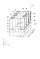
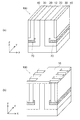
図1は、第1の実施形態に係る半導体装置の構成を例示する模式的斜視図である。
図1に表したように、本実施形態に係る半導体装置110においては、MOSFETのチャネル幅が基板の深さ方向に沿って設けられた、いわゆる3D(three-dimensional)型である。
半導体装置110は、第1半導体領域10、第2半導体領域20、第3半導体領域30、第4半導体領域40、ゲート領域50、ゲート絶縁膜60及び電界緩和領域70を備える。
図1は、第1の実施形態に係る半導体装置の構成を例示する模式的斜視図である。
図1に表したように、本実施形態に係る半導体装置110においては、MOSFETのチャネル幅が基板の深さ方向に沿って設けられた、いわゆる3D(three-dimensional)型である。
半導体装置110は、第1半導体領域10、第2半導体領域20、第3半導体領域30、第4半導体領域40、ゲート領域50、ゲート絶縁膜60及び電界緩和領域70を備える。
第1半導体領域10は、第1主面11aを含む第1部分11と、第1主面11aに対して直交する第1方向に延出した第2部分12と、を有する第1導電形の領域である。
なお、本実施形態では、第2部分12が延出する第1方向をZ方向、第1方向と直交する方向のうち一つ(第2方向)をX方向、第1方向及び第2方向と直交する第3方向をY方向とする。また、本実施形態では、説明の便宜上、Z方向に沿って第2部分12が延びる方向を「上」、これと反対方向を「下」とする。
本実施形態において、第1半導体領域10は、例えばシリコンのウェーハに燐(P)がドープされたn+ドレイン領域である。
なお、本実施形態では、第2部分12が延出する第1方向をZ方向、第1方向と直交する方向のうち一つ(第2方向)をX方向、第1方向及び第2方向と直交する第3方向をY方向とする。また、本実施形態では、説明の便宜上、Z方向に沿って第2部分12が延びる方向を「上」、これと反対方向を「下」とする。
本実施形態において、第1半導体領域10は、例えばシリコンのウェーハに燐(P)がドープされたn+ドレイン領域である。
第2半導体領域20は、第3部分23と、第4部分24と、を有する第1導電形の領域である。
第3部分23は、第1部分11の上において第2部分12のZ方向に沿った長さよりも短く設けられる。第4部分24は、第2部分12と隣接し第3部分23の上面の一部からZ方向に延出して設けられる。
すなわち、第2半導体領域20は、互いに直交する方向に設けられた第3部分23及び第4部分24により、XZ平面における断面視において、第1部分11及び第2部分12に沿った略L字型に設けられる。
第3部分23は、第1部分11の上において第2部分12のZ方向に沿った長さよりも短く設けられる。第4部分24は、第2部分12と隣接し第3部分23の上面の一部からZ方向に延出して設けられる。
すなわち、第2半導体領域20は、互いに直交する方向に設けられた第3部分23及び第4部分24により、XZ平面における断面視において、第1部分11及び第2部分12に沿った略L字型に設けられる。
本実施形態において、第2半導体領域20は、例えば第1半導体領域10の表面にエピタキシャル成長によって形成された膜である。第2半導体領域20は、例えばエピタキシャル成長膜に燐(P)がドープされたn−ドレイン領域である。第2半導体領域20は、MOSFETにおけるドリフト領域となる。
第3半導体領域30は、第5部分35と、第6部分36と、を有する第2導電形の領域である。
第5部分35は、第3部分23の上において第4部分24のZ方向に沿った長さよりも短く設けられる。第6部分36は、第4部分24と隣接し第5部分35の上面の一部からZ方向に延出して設けられる。
すなわち、第3半導体領域30は、互いに直交する方向に設けられた第5部分35及び第6部分36により、XZ平面における断面視において、第3部分23及び第4部分24に沿った略L字型に設けられる。
第5部分35は、第3部分23の上において第4部分24のZ方向に沿った長さよりも短く設けられる。第6部分36は、第4部分24と隣接し第5部分35の上面の一部からZ方向に延出して設けられる。
すなわち、第3半導体領域30は、互いに直交する方向に設けられた第5部分35及び第6部分36により、XZ平面における断面視において、第3部分23及び第4部分24に沿った略L字型に設けられる。
第3半導体領域30におけるZ方向に沿った長さh3は、第2半導体領域20におけるZ方向に沿った長さh4よりも短い。
本実施形態において、第3半導体領域30は、例えば第2半導体領域20の表面にエピタキシャル成長によって形成された膜である。第3半導体領域30は、例えばエピタキシャル成長膜にボロン(B)がドープされたp−ベース領域である。
本実施形態において、第3半導体領域30は、例えば第2半導体領域20の表面にエピタキシャル成長によって形成された膜である。第3半導体領域30は、例えばエピタキシャル成長膜にボロン(B)がドープされたp−ベース領域である。
第4半導体領域40は、第5部分35の上において第6部分36と隣接して設けられた第1導電形の領域である。
すなわち、第4半導体領域40は、第3半導体領域30上でZ方向に延在して設けられる。これにより、第4半導体領域40は、XZ平面における断面視において、第3半導体領域30の略L字型の内側に埋め込まれる。
すなわち、第4半導体領域40は、第3半導体領域30上でZ方向に延在して設けられる。これにより、第4半導体領域40は、XZ平面における断面視において、第3半導体領域30の略L字型の内側に埋め込まれる。
第4半導体領域40におけるZ方向に沿った長さh2は、第3半導体領域30におけるZ方向に沿った長さh3よりも短い。
本実施形態において、第4半導体領域40は、例えば第3半導体領域30上にエピタキシャル成長によって形成された膜である。第4半導体領域40は、例えばエピタキシャル成長膜に燐(P)がドープされたn+ソース領域である。
本実施形態において、第4半導体領域40は、例えば第3半導体領域30上にエピタキシャル成長によって形成された膜である。第4半導体領域40は、例えばエピタキシャル成長膜に燐(P)がドープされたn+ソース領域である。
ゲート領域50は、第2半導体領域20、第3半導体領域30及び第4半導体領域40をX方向に貫通するトレンチ100T内に設けられている。
すなわち、第2半導体領域20の第4部分24、第3半導体領域30の第6部分36及び第4半導体領域40は、X方向に沿って隣接している。トレンチ100Tは、この隣接する第4部分24、第6部分36及び第4半導体領域40をX方向に沿って貫通するよう設けられる。ゲート領域50は、トレンチ100T内に、後述のゲート絶縁膜60を介して埋め込まれる。
すなわち、第2半導体領域20の第4部分24、第3半導体領域30の第6部分36及び第4半導体領域40は、X方向に沿って隣接している。トレンチ100Tは、この隣接する第4部分24、第6部分36及び第4半導体領域40をX方向に沿って貫通するよう設けられる。ゲート領域50は、トレンチ100T内に、後述のゲート絶縁膜60を介して埋め込まれる。
また、ゲート領域50は、トレンチ100T内においてZ方向に沿って延びるよう設けられている。ゲート領域50は、Z方向に沿って長さh1で設けられている。長さh1は、例えば第4半導体領域の長さh2よりも短い。ゲート領域50としては、例えば多結晶シリコンが用いられる。
ゲート絶縁膜60は、トレンチ100Tの内壁と、ゲート領域50と、の間に設けられている。ゲート絶縁膜60としては、例えば酸化シリコン膜が用いられる。
電界緩和領域70は、第2半導体領域20の第3部分23と、第3半導体領域30の第5部分35と、の間に設けられている。電界緩和領域70は、第3半導体領域30の不純物濃度よりも低い不純物濃度を有する第2導電形の領域である。電界緩和領域70は、例えば第3部分23にボロン(B)がドープされたp−領域である。
電界緩和領域70は、第3部分23と、第5部分35と、の間から、第4部分24の一部に至るまで設けられている。すなわち、電界緩和領域70は、XZ平面の断面視において、第3半導体領域30の略L字型の隅部の外側の周辺に設けられている。このような電界緩和領域70が設けられると、p−形の第3半導体領域30とn−形の第2半導体領域20との間の急峻な不純物濃度変化が緩和される。すなわち、本実施形態に係る半導体装置110では、電界緩和領域70がリサーフ領域として機能し、第3半導体領域30の略L字型の隅部の周辺における電界集中を緩和する。
本実施形態に係る半導体装置110では、ゲート領域50にオン電圧を印加することで、ゲート絶縁膜60に隣接する第3半導体領域30であるp−ベース領域にチャネルが形成される。半導体装置110では、X方向に沿った第3半導体領域30の長さがチャネル長に対応する。また、半導体装置110では、第3半導体領域30におけるZ方向に沿った長さのうちゲート領域50と対応した深さh1がチャネル幅に対応する。第3半導体領域30におけるチャネル長方向の全体にチャネルが形成されると、ソース領域である第4半導体領域40からドリフト領域である第2半導体領域20を介してドレイン領域である第1半導体領域10へと電流が流れる。
一方、ゲート領域50にオン電圧が印加されない状態では、第3半導体領域30であるp−ベース領域にチャネルが形成されず、電流は流れない。本実施形態に係る半導体装置110では、第3半導体領域30と第2半導体領域20との間に電界緩和領域70が設けられているため、空乏層はチャネル領域から電界緩和領域70にまで達する。これにより、第3半導体領域30の隅部の周辺における電界集中を緩和して、耐圧を高めることができる。
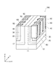
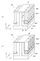
図2は、比較例に係る半導体装置を例示する模式的斜視図である。
図2に表したように、比較例に係る半導体装置190は、図1に表した半導体装置110のような電界緩和領域70が設けられていない。
図2に表した破線は、MOSFETがオフの状態での第3半導体領域30と第2半導体領域20との間に印加される電界を例示している。この半導体装置190では、第3半導体領域30の隅部周辺に電界が集中している。
図2に表したように、比較例に係る半導体装置190は、図1に表した半導体装置110のような電界緩和領域70が設けられていない。
図2に表した破線は、MOSFETがオフの状態での第3半導体領域30と第2半導体領域20との間に印加される電界を例示している。この半導体装置190では、第3半導体領域30の隅部周辺に電界が集中している。
半導体装置190においては、第1半導体領域10の第1部分11と第2部分12とで第2半導体領域20の2面(XY平面及びYZ平面)が囲まれている。そして、この第2半導体領域20の内側に第3半導体領域30が設けられている。このため、第3半導体領域30は、直交する2面(XY平面及びYZ平面)で第2半導体領域20と接する。よって、第3半導体領域30の上記2面で挟まれる隅部には、電界が集中しやすくなる。
第3半導体領域30の第5部分35から第1半導体領域10の第1部分11に向かう領域は、いわゆる3D−MOSFETの終端領域と等価であると考えられる。このため、第3半導体領域30の上記2面で挟まれる隅部の周辺に電界が集中すると、終端領域での耐圧の低下と同等であり、半導体装置190の全体の耐圧の低下につながる。
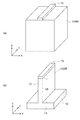
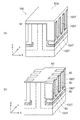
図3は、本実施形態に係る半導体装置の電界の状態を例示する模式的斜視図である。
図3に表した破線は、本実施形態に係る半導体装置110のMOSFETがオフの状態での第3半導体領域30と第2半導体領域20との間に印加される電界を例示している。
本実施形態に係る半導体装置110では、先に説明したように電界緩和領域70を備えることから、第3半導体領域30と第2半導体領域20との間のうち、特に第3半導体領域30の隅部の周辺での電界の集中が緩和される。これにより、図2に例示した比較例に係る半導体装置190に比べ、終端領域での耐圧を向上でき、半導体装置110の全体での耐圧を向上できるようになる。
図3に表した破線は、本実施形態に係る半導体装置110のMOSFETがオフの状態での第3半導体領域30と第2半導体領域20との間に印加される電界を例示している。
本実施形態に係る半導体装置110では、先に説明したように電界緩和領域70を備えることから、第3半導体領域30と第2半導体領域20との間のうち、特に第3半導体領域30の隅部の周辺での電界の集中が緩和される。これにより、図2に例示した比較例に係る半導体装置190に比べ、終端領域での耐圧を向上でき、半導体装置110の全体での耐圧を向上できるようになる。
図1に例示した半導体装置110では、第1半導体領域10の第2部分12がY方向に沿って延びるよう設けられている。また、半導体装置110では、第3半導体領域30及び第4半導体領域40が、Y方向に沿って延在している。さらに、半導体装置110では、複数のゲート領域50及びゲート絶縁膜60が、Y方向に沿って配置されている。
これにより、Y方向に延びる第2部分12に対応して複数のMOSFET構造を備えることになる。複数のMOSFET構造における各ゲート領域は、例えば並列に接続される。また、複数のMOSFET構造における各ソース領域は、例えば並列に接続される。
これにより、Y方向に延びる第2部分12に対応して複数のMOSFET構造を備えることになる。複数のMOSFET構造における各ゲート領域は、例えば並列に接続される。また、複数のMOSFET構造における各ソース領域は、例えば並列に接続される。
また、図1に例示した半導体装置110では、第2部分12を中心として、X方向に沿った両側に、第2半導体領域20、第3半導体領域30、第4半導体領域、複数のゲート領域50及び複数のゲート絶縁膜60が設けられている。
半導体装置110では、複数の第2部分12がX方向に沿って配置され、各第2部分12を中心としてX方向に沿った両側に、複数のMOSFET構造を備えるようにしてもよい。
半導体装置110では、複数の第2部分12がX方向に沿って配置され、各第2部分12を中心としてX方向に沿った両側に、複数のMOSFET構造を備えるようにしてもよい。
このような本実施形態に係る半導体装置110では、第3半導体領域30の隅部の周辺での電界の集中を緩和することによって、耐圧の向上を図ることができるようになる。
(第2の実施形態)
次に、第2の実施形態を説明する。第2の実施形態は、第1の実施形態に係る半導体装置の製造方法である。
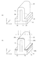
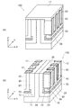
図4〜図10は、第1の実施形態に係る半導体装置の製造方法を説明する模式的斜視図である。
次に、第2の実施形態を説明する。第2の実施形態は、第1の実施形態に係る半導体装置の製造方法である。
図4〜図10は、第1の実施形態に係る半導体装置の製造方法を説明する模式的斜視図である。
先ず、図4(a)に表したように、例えばシリコンのウェーハ10Wを用意する。ウェーハ10Wには、第1半導体領域10であるドレイン領域となるように、例えば燐(P)がドープされ、n+になっている。ウェーハ10Wの不純物濃度は、例えば4.5×1019cm−3である。
次に、ウェーハ10Wの上に、例えばシリコン酸化膜15を形成し、フォトリソグラフィ及びエッチングによってパターン形成する。シリコン酸化膜15は、パターン形成によって、後述する第2部分12を形成する部分のみが残されている。
次に、図4(b)に表したように、パターニング形成されたシリコン酸化膜15をマスクとして、ウェーハ10Wをエッチングする。エッチングは、例えばRIE(Reactive Ion Etching)を用いる。ウェーハ10Wのエッチングによって残った部分が第1部分11となる。また、シリコン酸化膜15によってマスクされエッチングされなかった部分は第2部分12となる。これにより、第1部分11及び第2部分12を有する第1半導体領域10が形成される。
ここで、ウェーハ10Wのエッチング深さは、例えば15マイクロメートル(μm)〜20μmである。これにより、第2部分12のZ方向に沿った長さh5は、15μm〜20μmとなる。
ウェーハ10Wをエッチングした後は、シリコン酸化膜15を除去する。
ここで、ウェーハ10Wのエッチング深さは、例えば15マイクロメートル(μm)〜20μmである。これにより、第2部分12のZ方向に沿った長さh5は、15μm〜20μmとなる。
ウェーハ10Wをエッチングした後は、シリコン酸化膜15を除去する。
次に、図5(a)に表したように、第1半導体領域10の表面に、第2半導体領域20を成膜する。第2半導体領域20は、第1半導体領域10の表面に例えばエピタキシャル成長によって形成される。第2半導体領域20は、エピタキシャル成長によって約2μmの厚さで形成される。第2半導体領域20は、第1半導体領域10の第1部分11及び第2部分12の表面を覆うように形成される。これにより、第1部分11の上に第3部分23が形成され、第2部分12に隣接した第4部分24が形成される。
エピタキシャル成長後、第2半導体領域20には例えば燐(P)がドーピングされる。これにより、第2半導体領域20は、n−のドレイン領域となる。第2半導体領域20の不純物濃度は、例えば2×1016cm−3である。
エピタキシャル成長後、第2半導体領域20には例えば燐(P)がドーピングされる。これにより、第2半導体領域20は、n−のドレイン領域となる。第2半導体領域20の不純物濃度は、例えば2×1016cm−3である。
次に、図5(b)に表したように、第2半導体領域20の上からイオン注入を行う。イオン注入は、不純物として例えばボロン(B)のイオンを注入し、p−とする。ここで、ボロン(B)のイオンは、第2半導体領域20の上面20c及び第1半導体領域10の第1主面10aと対向する第2主面20aに注入される。このうち、第2主面20aに注入されたボロン(B)によるp−領域が、電界緩和領域70となる。
p−領域(電界緩和領域70)の不純物濃度は、後に形成する第3半導体領域30の不純物濃度よりも低い。ここで行うイオン注入は、例えば、ボロンをドーズ量1×1014cm−2で注入する。これにより、p−領域(電界緩和領域70)の不純物濃度は、1×1018cm−3未満となる。
また、イオン注入におけるイオンの入射角度は、第2半導体領域20における第2主面20aにはイオンが注入され、第2半導体領域における、第2部分12の側面と対向する第3主面20bにはイオンが注入されない角度である。イオンの入射角度は、例えば、第2主面20aと垂直な方向に対して約3度である。これにより、第2半導体領域20の第3主面20bにイオンが衝突しても弾かれて注入されず、第2主面20aには注入される。なお、上面20cにも不純物が注入されるが、後の工程で研削によって除去される。
第2半導体領域20に不純物を注入した後は、熱処理によって不純物を拡散させる。
第2半導体領域20に不純物を注入した後は、熱処理によって不純物を拡散させる。
次に、図6(a)に表したように、第2半導体領域20の表面に、第3半導体領域30を成膜する。第3半導体領域30は、第2半導体領域20の表面に例えばエピタキシャル成長によって形成される。第3半導体領域30は、エピタキシャル成長によって約0.35μmの厚さで形成される。これにより、第3部分23の上に第5部分35が形成され、第4部分24に隣接した第6部分36が形成される。
エピタキシャル成長後、第3半導体領域30には例えばボロン(B)がドープされ、p−のベース領域となる。第3半導体領域30の不純物濃度は、例えば1×1018cm−3である。すなわち、先に形成した電界緩和領域70の不純物濃度よりも高い。
エピタキシャル成長後、第3半導体領域30には例えばボロン(B)がドープされ、p−のベース領域となる。第3半導体領域30の不純物濃度は、例えば1×1018cm−3である。すなわち、先に形成した電界緩和領域70の不純物濃度よりも高い。
次に、図6(b)に表したように、第3半導体領域30の表面に、第4半導体領域40を成膜する。第4半導体領域40は、第3半導体領域30の表面に例えばエピタキシャル成長によって形成される。第4半導体領域40は、エピタキシャル成長によって約0.55μmの厚さで形成される。これにより、第4半導体領域40は、第5部分35の上において第6部分36と隣接して設けられる。
エピタキシャル成長後、第4半導体領域40には例えば燐(P)がドープされ、n+のソース領域となる。第4半導体領域40の不純物濃度は、例えば3×1019cm−3である。
エピタキシャル成長後、第4半導体領域40には例えば燐(P)がドープされ、n+のソース領域となる。第4半導体領域40の不純物濃度は、例えば3×1019cm−3である。
次に、図7(a)に表したように、第4半導体領域40、第3半導体領域30及び第2半導体領域20を、第1半導体領域10の第2部分12が露出するまで除去する。この除去方法には、例えばCMP(Chemical Mechanical Polishing)が用いられる。CMPによって、第2部分12の露出面が平坦化された構造体100が構成される。
次に、図7(b)に表したように、構造体100の上にマスク材16を形成する。マスク材16には、例えば酸化シリコンが用いられる。マスク材16は、例えばCVD(Chemical Vapor Deposition)によって形成される。マスク材16を形成した後は、フォトリソグラフィ及びエッチングによってマスク材16のパターニング形成を行う。例えば、マスク材16の上にレジスト(図示せず)を塗布し、フォトリソグラフィ及びエッチングによってパターニング形成する。その後、レジストをマスクとして、例えばRIEによりマスク材16をエッチングし、パターニング形成する。このパターニング形成では、ゲート領域50及びゲート絶縁膜60を形成する部分のみ、マスク材16に開口が形成される。マスク材16のパターニング形成後は、レジストを除去する。
次に、図8(a)に表したように、パターニング形成したマスク材16をマスクとして構造体100をエッチングする。このエッチングによって、マスク材16の開口部分の構造体100が彫り込まれ、トレンチ100Tとなる。トレンチ100Tは、X方向に沿って、第2半導体領域20、第3半導体領域30及び第4半導体領域40を貫通するよう設けられる。また、トレンチ100Tは、Y方向に沿って約1μmの幅、Z方向に沿って、約15μm〜20μmの長さht1、で形成される。本実施形態では、トレンチ100TのZ方向に沿った長さht1は、第4半導体領域40のZ方向に沿った長さh2よりも短い。また、必要に応じて、複数のトレンチ100Tが、Y方向及びX方向に沿って設けられる。
トレンチ100Tを形成した後は、マスク材16を除去する。
トレンチ100Tを形成した後は、マスク材16を除去する。
次に、図8(b)に表したように、トレンチ100Tが形成された構造体100の上にゲート絶縁膜60を成膜する。ゲート絶縁膜60は、例えばシリコン酸化膜である。シリコン酸化膜は、例えば熱酸化によって形成される。ゲート絶縁膜60は、例えば100ナノメートル(nm)の厚さで形成される。
次に、図9(a)に表したように、ゲート絶縁膜60の上に、ゲート材料50Aを形成する。ゲート材料50Aは、例えば多結晶シリコンである。ゲート材料50Aは、構造体100の上面及びトレンチ100T内に埋め込まれる。
次に、ゲート材料50Aをエッチバックする。これにより、図9(b)に表したように、トレンチ100Tの中にゲート絶縁膜60を介して設けられたゲート領域50が形成される。ゲート材料50Aのエッチバックによって形成されたゲート領域50の上面は、トレンチ100Tの開口よりもZ方向に沿ってわずかに低くなっている。
次に、図10(a)に表したように、構造体100の上に層間絶縁膜17を形成する。層間絶縁膜17は、構造体100の上面の全面に形成される。その後、層間絶縁膜17を例えばRIEによってエッチングする。このエッチングは、図10(b)に表したように、第2部分12、第2半導体領域20、第3半導体領域30及び第4半導体領域40が露出するまで行う。これにより、ゲート領域50の上に層間絶縁膜17が残る状態になる。
このあとは、ゲート領域50、第1半導体領域10であるドレイン領域及び第4半導体領域40であるソース領域に導通する図示しない電極(ゲート電極、ドレイン電極及びソース電極)を形成する。電極には、例えばアルミニウム(Al)が用いられる。電極は、フォトリソグラフィ及びエッチングによって所定のパターニング形状にされる。その後、例えばポリイミド等の保護膜(図示せず)を形成する。これにより半導体装置110が完成する。
このような第2の実施形態によれば、第3半導体領域30と第2半導体領域20との間に電界緩和領域70を備え、電界集中を緩和して耐圧を向上した半導体装置110を製造することが可能となる。
なお、前述の各実施形態においては、第1導電形をn形、第2導電形をp形として説明したが、本発明は第1導電形をp形、第2導電形をn形としても実施可能である。さらにまた、前述の各実施形態においては、半導体としてシリコン(Si)を用いたMOSFETを説明したが、半導体としては、例えばシリコンカーバイト(SiC)若しくは窒化ガリウム(GaN)等の化合物半導体、またはダイアモンド等のワイドバンドギャップ半導体を用いることもできる。
さらにまた、前述の各実施の形態および各変形例においては、MOSFETである例を示したが、本発明はこれに限定されず、半導体装置は、例えば、MOSFETとSBD(Schottky Barrier Diode:ショットキーバリアダイオード)との混載素子、またはIGBT(Insulated Gate Bipolar Transistor)などの素子でもよい。
以上説明したように、本実施形態によれば、半導体装置の耐圧を向上することができるようになる。
本発明のいくつかの実施形態を説明したが、これらの実施形態は、例として提示したものであり、発明の範囲を限定することは意図していない。これら新規な実施形態は、その他の様々な形態で実施されることが可能であり、発明の要旨を逸脱しない範囲で、種々の省略、置き換え、変更を行うことができる。これら実施形態やその変形は、発明の範囲や要旨に含まれるとともに、特許請求の範囲に記載された発明とその均等の範囲に含まれる。
10…第1半導体領域、11…第1部分、11a…第1主面、12…第2部分、20…第2半導体領域、30…第3半導体領域、40…第4半導体領域、50…ゲート領域、60…ゲート絶縁膜、70…電界緩和領域
Claims (8)
- 第1主面を含む第1部分と、前記第1主面に対して直交する第1方向に延出した第2部分と、を有する第1導電形の第1半導体領域と、
前記第1部分の側において前記第2部分の前記第1方向に沿った長さよりも短く設けられた第3部分と、前記第2部分と隣接し前記第3部分の上面の一部から前記第1方向に延出した第4部分と、を有する第1導電形の第2半導体領域と、
前記第3部分の側において前記第4部分の前記第1方向に沿った長さよりも短く設けられた第5部分と、前記第4部分と隣接し前記第5部分の上面の一部から前記第1方向に延出した第6部分と、を有する第2導電形の第3半導体領域と、
前記第5部分の上において前記第6部分と隣接して設けられた第1導電形の第4半導体領域と、
前記第1方向と直交する第2方向であって、前記第2半導体領域、前記第3半導体領域及び前記第4半導体領域に形成されたトレンチ内に設けられたゲート領域と、
前記トレンチの内壁と、前記ゲート領域と、の間に設けられたゲート絶縁膜と、
前記第3部分と、前記第5部分と、の間に設けられ、前記第3半導体領域の不純物濃度よりも低い不純物濃度を有する第2導電形の電界緩和領域と、
を備えたことを特徴とする半導体装置。 - 前記第2部分は、前記第1方向及び前記第2方向と直交する第3方向に延びるよう設けられたことを特徴とする請求項1記載の半導体装置。
- 前記第3方向に沿って、複数の前記ゲート領域及び複数の前記ゲート絶縁膜が設けられたことを特徴とする請求項2記載の半導体装置。
- 前記第2半導体領域、前記第3半導体領域及び前記第4半導体領域は、前記第3方向に沿って延在することを特徴とする請求項2または3に記載の半導体装置。
- 前記ゲート領域の前記第1方向に沿った第1の長さは、前記第4半導体領域の前記第1方向に沿った第2の長さよりも低いことを特徴とする請求項1〜4のいずれか1つに記載の半導体装置。
- 第1主面を含む第1部分と、前記第1主面に対して直交する第1方向に延出した第2部分と、を有する第1導電形の第1半導体領域を形成する工程と、
前記第1半導体領域を第1導電形の第2半導体領域で覆い、前記第1部分の側において前記第2部分の前記第1方向に沿った長さよりも短く設けられた第3部分と、前記第2部分と隣接し前記第3部分の上面の一部から前記第1方向に延出した第4部分と、を形成する工程と、
前記3部分における、前記第1主面と対向した第2主面に、第2導電形の電界緩和領域を形成する工程と、
前記第2半導体領域を第2導電形の第3半導体領域で覆い、前記第3部分の側において前記第4部分の前記第1方向に沿った長さよりも短く設けられた第5部分と、前記第4部分と隣接し前記第5部分の上面の一部から前記第1方向に延出した第6部分と、を形成する工程と、
前記第3半導体領域を第1導電形の第4半導体領域で覆う工程と、
前記第4半導体領域、前記第3半導体領域及び前記第2半導体領域を、前記第2部分が露出するまで除去する工程と、
前記第1方向と直交する第2方向であって、前記第2半導体領域、前記第3半導体領域及び前記第4半導体領域にトレンチを形成し、前記トレンチ内にゲート絶縁膜を介してゲート領域を形成する工程と、
を備えたことを特徴とする半導体装置の製造方法。 - 前記電界緩和領域を形成する工程では、前記第2主面に第2導電形となる不純物のイオンを注入することを特徴とする請求項6記載の半導体装置の製造方法。
- 前記イオンの入射角度は、前記第2主面には前記イオンが注入され、前記第4部分における前記第2部分の側面と対向した第3主面には前記イオンが注入されない角度であることを特徴とする請求項7記載の半導体装置の製造方法。
Priority Applications (4)
| Application Number | Priority Date | Filing Date | Title |
|---|---|---|---|
| JP2010183398A JP2012043955A (ja) | 2010-08-18 | 2010-08-18 | 半導体装置及びその製造方法 |
| CN2011100519452A CN102376764A (zh) | 2010-08-18 | 2011-03-03 | 半导体装置及其制造方法 |
| US13/053,452 US20120043606A1 (en) | 2010-08-18 | 2011-03-22 | Semiconductor device and method for manufacturing same |
| EP11159170A EP2421047A1 (en) | 2010-08-18 | 2011-03-22 | Semiconductor device and method for manufacturing same |
Applications Claiming Priority (1)
| Application Number | Priority Date | Filing Date | Title |
|---|---|---|---|
| JP2010183398A JP2012043955A (ja) | 2010-08-18 | 2010-08-18 | 半導体装置及びその製造方法 |
Publications (2)
| Publication Number | Publication Date |
|---|---|
| JP2012043955A true JP2012043955A (ja) | 2012-03-01 |
| JP2012043955A5 JP2012043955A5 (ja) | 2012-10-11 |
Family
ID=44262919
Family Applications (1)
| Application Number | Title | Priority Date | Filing Date |
|---|---|---|---|
| JP2010183398A Abandoned JP2012043955A (ja) | 2010-08-18 | 2010-08-18 | 半導体装置及びその製造方法 |
Country Status (4)
| Country | Link |
|---|---|
| US (1) | US20120043606A1 (ja) |
| EP (1) | EP2421047A1 (ja) |
| JP (1) | JP2012043955A (ja) |
| CN (1) | CN102376764A (ja) |
Cited By (3)
| Publication number | Priority date | Publication date | Assignee | Title |
|---|---|---|---|---|
| WO2015177914A1 (ja) * | 2014-05-23 | 2015-11-26 | 株式会社日立製作所 | 半導体装置、半導体装置の製造方法、電力変換装置、3相モータシステム、自動車、および鉄道車両 |
| WO2016116998A1 (ja) * | 2015-01-19 | 2016-07-28 | 株式会社日立製作所 | 半導体装置及びその製造方法、電力変換装置、3相モータシステム、自動車、並びに鉄道車両 |
| JPWO2016129068A1 (ja) * | 2015-02-12 | 2017-06-22 | 株式会社日立製作所 | 半導体装置及びその製造方法、電力変換装置、3相モータシステム、自動車並びに鉄道車両 |
Families Citing this family (3)
| Publication number | Priority date | Publication date | Assignee | Title |
|---|---|---|---|---|
| JP2016096307A (ja) * | 2014-11-17 | 2016-05-26 | トヨタ自動車株式会社 | 半導体装置 |
| US10903163B2 (en) | 2015-10-19 | 2021-01-26 | Vishay-Siliconix, LLC | Trench MOSFET with self-aligned body contact with spacer |
| JP7075876B2 (ja) * | 2018-12-25 | 2022-05-26 | 株式会社日立製作所 | 炭化ケイ素半導体装置、電力変換装置、3相モータシステム、自動車および鉄道車両 |
Family Cites Families (7)
| Publication number | Priority date | Publication date | Assignee | Title |
|---|---|---|---|---|
| JP3356162B2 (ja) * | 1999-10-19 | 2002-12-09 | 株式会社デンソー | 半導体装置及びその製造方法 |
| US6642577B2 (en) * | 2000-03-16 | 2003-11-04 | Denso Corporation | Semiconductor device including power MOSFET and peripheral device and method for manufacturing the same |
| JP2002231945A (ja) * | 2001-02-06 | 2002-08-16 | Denso Corp | 半導体装置の製造方法 |
| JP3534084B2 (ja) * | 2001-04-18 | 2004-06-07 | 株式会社デンソー | 半導体装置およびその製造方法 |
| US7161208B2 (en) * | 2002-05-14 | 2007-01-09 | International Rectifier Corporation | Trench mosfet with field relief feature |
| JP2007221024A (ja) * | 2006-02-20 | 2007-08-30 | Toshiba Corp | 半導体装置 |
| US8004051B2 (en) * | 2009-02-06 | 2011-08-23 | Texas Instruments Incorporated | Lateral trench MOSFET having a field plate |
-
2010
- 2010-08-18 JP JP2010183398A patent/JP2012043955A/ja not_active Abandoned
-
2011
- 2011-03-03 CN CN2011100519452A patent/CN102376764A/zh active Pending
- 2011-03-22 US US13/053,452 patent/US20120043606A1/en not_active Abandoned
- 2011-03-22 EP EP11159170A patent/EP2421047A1/en not_active Withdrawn
Cited By (7)
| Publication number | Priority date | Publication date | Assignee | Title |
|---|---|---|---|---|
| WO2015177914A1 (ja) * | 2014-05-23 | 2015-11-26 | 株式会社日立製作所 | 半導体装置、半導体装置の製造方法、電力変換装置、3相モータシステム、自動車、および鉄道車両 |
| JPWO2015177914A1 (ja) * | 2014-05-23 | 2017-04-20 | 株式会社日立製作所 | 半導体装置、半導体装置の製造方法、電力変換装置、3相モータシステム、自動車、および鉄道車両 |
| WO2016116998A1 (ja) * | 2015-01-19 | 2016-07-28 | 株式会社日立製作所 | 半導体装置及びその製造方法、電力変換装置、3相モータシステム、自動車、並びに鉄道車両 |
| US9960259B2 (en) | 2015-01-19 | 2018-05-01 | Hitachi, Ltd. | Semiconductor device, method for manufacturing same, power conversion device, three-phase motor system, automobile, and railway carriage |
| JPWO2016129068A1 (ja) * | 2015-02-12 | 2017-06-22 | 株式会社日立製作所 | 半導体装置及びその製造方法、電力変換装置、3相モータシステム、自動車並びに鉄道車両 |
| US10290704B2 (en) | 2015-02-12 | 2019-05-14 | Hitachi, Ltd. | Semiconductor device and method for manufacturing same, power conversion device, three-phase motor system, automobile, and railway carriage |
| DE112015004751B4 (de) | 2015-02-12 | 2020-07-09 | Hitachi, Ltd. | Halbleitervorrichtung und verfahren zu deren herstellung, leistungsumsetzervorrichtung, dreiphasenmotorsystem, kraftfahrzeug und eisenbahnwagen |
Also Published As
| Publication number | Publication date |
|---|---|
| CN102376764A (zh) | 2012-03-14 |
| US20120043606A1 (en) | 2012-02-23 |
| EP2421047A1 (en) | 2012-02-22 |
Similar Documents
| Publication | Publication Date | Title |
|---|---|---|
| JP7283107B2 (ja) | 絶縁ゲート型半導体装置及びその製造方法 | |
| JP5188037B2 (ja) | 半導体装置 | |
| JP7059555B2 (ja) | 半導体装置 | |
| JP5586887B2 (ja) | 半導体装置及びその製造方法 | |
| US20120070965A1 (en) | Semiconductor device and manufacturing method for the same | |
| JPWO2017064949A1 (ja) | 半導体装置および半導体装置の製造方法 | |
| JP2008182054A (ja) | 半導体装置 | |
| JP6855700B2 (ja) | 半導体装置およびその製造方法 | |
| US20130146886A1 (en) | Vertical GaN JFET with Gate Source Electrodes on Regrown Gate | |
| JP2012204529A (ja) | 半導体装置及びその製造方法 | |
| JP2014146666A (ja) | 半導体装置 | |
| JP2013214661A (ja) | 炭化珪素半導体装置およびその製造方法 | |
| JP2011054885A (ja) | 半導体装置及び半導体装置の製造方法 | |
| JP5878331B2 (ja) | 半導体装置及びその製造方法 | |
| US10439060B2 (en) | Semiconductor device and method of manufacturing semiconductor device | |
| JP2017092355A (ja) | 半導体装置および半導体装置の製造方法 | |
| JP2018041853A (ja) | 半導体装置および半導体装置の製造方法 | |
| JP2023153392A (ja) | 半導体装置 | |
| KR101710815B1 (ko) | 반도체 디바이스의 제조 방법 | |
| JP2012043955A (ja) | 半導体装置及びその製造方法 | |
| JP5463725B2 (ja) | 炭化珪素半導体装置およびその製造方法 | |
| JP2010153622A (ja) | 半導体素子 | |
| TW201607025A (zh) | 半導體裝置 | |
| JP2023101772A (ja) | 半導体装置および半導体装置の製造方法 | |
| JP2014187320A (ja) | 半導体装置 |
Legal Events
| Date | Code | Title | Description |
|---|---|---|---|
| A521 | Request for written amendment filed |
Free format text: JAPANESE INTERMEDIATE CODE: A523 Effective date: 20120828 |
|
| A621 | Written request for application examination |
Free format text: JAPANESE INTERMEDIATE CODE: A621 Effective date: 20120828 |
|
| A762 | Written abandonment of application |
Free format text: JAPANESE INTERMEDIATE CODE: A762 Effective date: 20130704 |