EP2421047A1 - Semiconductor device and method for manufacturing same - Google Patents
Semiconductor device and method for manufacturing same Download PDFInfo
- Publication number
- EP2421047A1 EP2421047A1 EP11159170A EP11159170A EP2421047A1 EP 2421047 A1 EP2421047 A1 EP 2421047A1 EP 11159170 A EP11159170 A EP 11159170A EP 11159170 A EP11159170 A EP 11159170A EP 2421047 A1 EP2421047 A1 EP 2421047A1
- Authority
- EP
- European Patent Office
- Prior art keywords
- semiconductor region
- region
- length
- along
- semiconductor
- Prior art date
- Legal status (The legal status is an assumption and is not a legal conclusion. Google has not performed a legal analysis and makes no representation as to the accuracy of the status listed.)
- Withdrawn
Links
- 239000004065 semiconductor Substances 0.000 title claims abstract description 248
- 238000000034 method Methods 0.000 title claims description 21
- 238000004519 manufacturing process Methods 0.000 title claims description 8
- 230000005684 electric field Effects 0.000 claims abstract description 42
- 239000012535 impurity Substances 0.000 claims abstract description 30
- 150000002500 ions Chemical class 0.000 claims description 12
- 238000010438 heat treatment Methods 0.000 claims description 2
- 239000007943 implant Substances 0.000 claims description 2
- 239000000463 material Substances 0.000 description 17
- VYPSYNLAJGMNEJ-UHFFFAOYSA-N Silicium dioxide Chemical compound O=[Si]=O VYPSYNLAJGMNEJ-UHFFFAOYSA-N 0.000 description 9
- 230000015556 catabolic process Effects 0.000 description 9
- 238000005530 etching Methods 0.000 description 9
- 229910052814 silicon oxide Inorganic materials 0.000 description 9
- ZOXJGFHDIHLPTG-UHFFFAOYSA-N Boron Chemical compound [B] ZOXJGFHDIHLPTG-UHFFFAOYSA-N 0.000 description 7
- 229910052796 boron Inorganic materials 0.000 description 7
- OAICVXFJPJFONN-UHFFFAOYSA-N Phosphorus Chemical compound [P] OAICVXFJPJFONN-UHFFFAOYSA-N 0.000 description 6
- 229910052698 phosphorus Inorganic materials 0.000 description 6
- 239000011574 phosphorus Substances 0.000 description 6
- 238000000059 patterning Methods 0.000 description 5
- XUIMIQQOPSSXEZ-UHFFFAOYSA-N Silicon Chemical compound [Si] XUIMIQQOPSSXEZ-UHFFFAOYSA-N 0.000 description 4
- 239000011229 interlayer Substances 0.000 description 4
- 238000000206 photolithography Methods 0.000 description 4
- 238000001020 plasma etching Methods 0.000 description 4
- 229910052710 silicon Inorganic materials 0.000 description 4
- 239000010703 silicon Substances 0.000 description 4
- 238000005468 ion implantation Methods 0.000 description 3
- 238000005229 chemical vapour deposition Methods 0.000 description 2
- 239000012141 concentrate Substances 0.000 description 2
- 230000004048 modification Effects 0.000 description 2
- 238000012986 modification Methods 0.000 description 2
- 238000005498 polishing Methods 0.000 description 2
- 229910021420 polycrystalline silicon Inorganic materials 0.000 description 2
- 239000000758 substrate Substances 0.000 description 2
- JMASRVWKEDWRBT-UHFFFAOYSA-N Gallium nitride Chemical compound [Ga]#N JMASRVWKEDWRBT-UHFFFAOYSA-N 0.000 description 1
- 239000004642 Polyimide Substances 0.000 description 1
- 229910052782 aluminium Inorganic materials 0.000 description 1
- XAGFODPZIPBFFR-UHFFFAOYSA-N aluminium Chemical compound [Al] XAGFODPZIPBFFR-UHFFFAOYSA-N 0.000 description 1
- 230000004888 barrier function Effects 0.000 description 1
- 230000008859 change Effects 0.000 description 1
- 150000001875 compounds Chemical class 0.000 description 1
- 229910003460 diamond Inorganic materials 0.000 description 1
- 239000010432 diamond Substances 0.000 description 1
- 230000005669 field effect Effects 0.000 description 1
- 230000006872 improvement Effects 0.000 description 1
- 239000010410 layer Substances 0.000 description 1
- 230000003647 oxidation Effects 0.000 description 1
- 238000007254 oxidation reaction Methods 0.000 description 1
- 229920001721 polyimide Polymers 0.000 description 1
- 230000008569 process Effects 0.000 description 1
- 230000001681 protective effect Effects 0.000 description 1
- HBMJWWWQQXIZIP-UHFFFAOYSA-N silicon carbide Chemical compound [Si+]#[C-] HBMJWWWQQXIZIP-UHFFFAOYSA-N 0.000 description 1
- 239000000126 substance Substances 0.000 description 1
- 238000006467 substitution reaction Methods 0.000 description 1
Images


Classifications
-
- H—ELECTRICITY
- H01—ELECTRIC ELEMENTS
- H01L—SEMICONDUCTOR DEVICES NOT COVERED BY CLASS H10
- H01L29/00—Semiconductor devices adapted for rectifying, amplifying, oscillating or switching, or capacitors or resistors with at least one potential-jump barrier or surface barrier, e.g. PN junction depletion layer or carrier concentration layer; Details of semiconductor bodies or of electrodes thereof ; Multistep manufacturing processes therefor
- H01L29/66—Types of semiconductor device ; Multistep manufacturing processes therefor
- H01L29/68—Types of semiconductor device ; Multistep manufacturing processes therefor controllable by only the electric current supplied, or only the electric potential applied, to an electrode which does not carry the current to be rectified, amplified or switched
- H01L29/76—Unipolar devices, e.g. field effect transistors
- H01L29/772—Field effect transistors
- H01L29/78—Field effect transistors with field effect produced by an insulated gate
- H01L29/7801—DMOS transistors, i.e. MISFETs with a channel accommodating body or base region adjoining a drain drift region
- H01L29/7816—Lateral DMOS transistors, i.e. LDMOS transistors
- H01L29/7825—Lateral DMOS transistors, i.e. LDMOS transistors with trench gate electrode
-
- H—ELECTRICITY
- H01—ELECTRIC ELEMENTS
- H01L—SEMICONDUCTOR DEVICES NOT COVERED BY CLASS H10
- H01L29/00—Semiconductor devices adapted for rectifying, amplifying, oscillating or switching, or capacitors or resistors with at least one potential-jump barrier or surface barrier, e.g. PN junction depletion layer or carrier concentration layer; Details of semiconductor bodies or of electrodes thereof ; Multistep manufacturing processes therefor
- H01L29/02—Semiconductor bodies ; Multistep manufacturing processes therefor
- H01L29/06—Semiconductor bodies ; Multistep manufacturing processes therefor characterised by their shape; characterised by the shapes, relative sizes, or dispositions of the semiconductor regions ; characterised by the concentration or distribution of impurities within semiconductor regions
- H01L29/0603—Semiconductor bodies ; Multistep manufacturing processes therefor characterised by their shape; characterised by the shapes, relative sizes, or dispositions of the semiconductor regions ; characterised by the concentration or distribution of impurities within semiconductor regions characterised by particular constructional design considerations, e.g. for preventing surface leakage, for controlling electric field concentration or for internal isolations regions
- H01L29/0607—Semiconductor bodies ; Multistep manufacturing processes therefor characterised by their shape; characterised by the shapes, relative sizes, or dispositions of the semiconductor regions ; characterised by the concentration or distribution of impurities within semiconductor regions characterised by particular constructional design considerations, e.g. for preventing surface leakage, for controlling electric field concentration or for internal isolations regions for preventing surface leakage or controlling electric field concentration
- H01L29/0611—Semiconductor bodies ; Multistep manufacturing processes therefor characterised by their shape; characterised by the shapes, relative sizes, or dispositions of the semiconductor regions ; characterised by the concentration or distribution of impurities within semiconductor regions characterised by particular constructional design considerations, e.g. for preventing surface leakage, for controlling electric field concentration or for internal isolations regions for preventing surface leakage or controlling electric field concentration for increasing or controlling the breakdown voltage of reverse biased devices
- H01L29/0615—Semiconductor bodies ; Multistep manufacturing processes therefor characterised by their shape; characterised by the shapes, relative sizes, or dispositions of the semiconductor regions ; characterised by the concentration or distribution of impurities within semiconductor regions characterised by particular constructional design considerations, e.g. for preventing surface leakage, for controlling electric field concentration or for internal isolations regions for preventing surface leakage or controlling electric field concentration for increasing or controlling the breakdown voltage of reverse biased devices by the doping profile or the shape or the arrangement of the PN junction, or with supplementary regions, e.g. junction termination extension [JTE]
- H01L29/0619—Semiconductor bodies ; Multistep manufacturing processes therefor characterised by their shape; characterised by the shapes, relative sizes, or dispositions of the semiconductor regions ; characterised by the concentration or distribution of impurities within semiconductor regions characterised by particular constructional design considerations, e.g. for preventing surface leakage, for controlling electric field concentration or for internal isolations regions for preventing surface leakage or controlling electric field concentration for increasing or controlling the breakdown voltage of reverse biased devices by the doping profile or the shape or the arrangement of the PN junction, or with supplementary regions, e.g. junction termination extension [JTE] with a supplementary region doped oppositely to or in rectifying contact with the semiconductor containing or contacting region, e.g. guard rings with PN or Schottky junction
- H01L29/0623—Buried supplementary region, e.g. buried guard ring
-
- H—ELECTRICITY
- H01—ELECTRIC ELEMENTS
- H01L—SEMICONDUCTOR DEVICES NOT COVERED BY CLASS H10
- H01L29/00—Semiconductor devices adapted for rectifying, amplifying, oscillating or switching, or capacitors or resistors with at least one potential-jump barrier or surface barrier, e.g. PN junction depletion layer or carrier concentration layer; Details of semiconductor bodies or of electrodes thereof ; Multistep manufacturing processes therefor
- H01L29/02—Semiconductor bodies ; Multistep manufacturing processes therefor
- H01L29/06—Semiconductor bodies ; Multistep manufacturing processes therefor characterised by their shape; characterised by the shapes, relative sizes, or dispositions of the semiconductor regions ; characterised by the concentration or distribution of impurities within semiconductor regions
- H01L29/0603—Semiconductor bodies ; Multistep manufacturing processes therefor characterised by their shape; characterised by the shapes, relative sizes, or dispositions of the semiconductor regions ; characterised by the concentration or distribution of impurities within semiconductor regions characterised by particular constructional design considerations, e.g. for preventing surface leakage, for controlling electric field concentration or for internal isolations regions
- H01L29/0607—Semiconductor bodies ; Multistep manufacturing processes therefor characterised by their shape; characterised by the shapes, relative sizes, or dispositions of the semiconductor regions ; characterised by the concentration or distribution of impurities within semiconductor regions characterised by particular constructional design considerations, e.g. for preventing surface leakage, for controlling electric field concentration or for internal isolations regions for preventing surface leakage or controlling electric field concentration
- H01L29/0611—Semiconductor bodies ; Multistep manufacturing processes therefor characterised by their shape; characterised by the shapes, relative sizes, or dispositions of the semiconductor regions ; characterised by the concentration or distribution of impurities within semiconductor regions characterised by particular constructional design considerations, e.g. for preventing surface leakage, for controlling electric field concentration or for internal isolations regions for preventing surface leakage or controlling electric field concentration for increasing or controlling the breakdown voltage of reverse biased devices
- H01L29/0615—Semiconductor bodies ; Multistep manufacturing processes therefor characterised by their shape; characterised by the shapes, relative sizes, or dispositions of the semiconductor regions ; characterised by the concentration or distribution of impurities within semiconductor regions characterised by particular constructional design considerations, e.g. for preventing surface leakage, for controlling electric field concentration or for internal isolations regions for preventing surface leakage or controlling electric field concentration for increasing or controlling the breakdown voltage of reverse biased devices by the doping profile or the shape or the arrangement of the PN junction, or with supplementary regions, e.g. junction termination extension [JTE]
- H01L29/063—Reduced surface field [RESURF] pn-junction structures
- H01L29/0634—Multiple reduced surface field (multi-RESURF) structures, e.g. double RESURF, charge compensation, cool, superjunction (SJ), 3D-RESURF, composite buffer (CB) structures
-
- H—ELECTRICITY
- H01—ELECTRIC ELEMENTS
- H01L—SEMICONDUCTOR DEVICES NOT COVERED BY CLASS H10
- H01L29/00—Semiconductor devices adapted for rectifying, amplifying, oscillating or switching, or capacitors or resistors with at least one potential-jump barrier or surface barrier, e.g. PN junction depletion layer or carrier concentration layer; Details of semiconductor bodies or of electrodes thereof ; Multistep manufacturing processes therefor
- H01L29/66—Types of semiconductor device ; Multistep manufacturing processes therefor
- H01L29/66007—Multistep manufacturing processes
- H01L29/66075—Multistep manufacturing processes of devices having semiconductor bodies comprising group 14 or group 13/15 materials
- H01L29/66227—Multistep manufacturing processes of devices having semiconductor bodies comprising group 14 or group 13/15 materials the devices being controllable only by the electric current supplied or the electric potential applied, to an electrode which does not carry the current to be rectified, amplified or switched, e.g. three-terminal devices
- H01L29/66409—Unipolar field-effect transistors
- H01L29/66477—Unipolar field-effect transistors with an insulated gate, i.e. MISFET
- H01L29/66674—DMOS transistors, i.e. MISFETs with a channel accommodating body or base region adjoining a drain drift region
- H01L29/66681—Lateral DMOS transistors, i.e. LDMOS transistors
- H01L29/66704—Lateral DMOS transistors, i.e. LDMOS transistors with a step of recessing the gate electrode, e.g. to form a trench gate electrode
-
- H—ELECTRICITY
- H01—ELECTRIC ELEMENTS
- H01L—SEMICONDUCTOR DEVICES NOT COVERED BY CLASS H10
- H01L29/00—Semiconductor devices adapted for rectifying, amplifying, oscillating or switching, or capacitors or resistors with at least one potential-jump barrier or surface barrier, e.g. PN junction depletion layer or carrier concentration layer; Details of semiconductor bodies or of electrodes thereof ; Multistep manufacturing processes therefor
- H01L29/66—Types of semiconductor device ; Multistep manufacturing processes therefor
- H01L29/68—Types of semiconductor device ; Multistep manufacturing processes therefor controllable by only the electric current supplied, or only the electric potential applied, to an electrode which does not carry the current to be rectified, amplified or switched
- H01L29/70—Bipolar devices
- H01L29/72—Transistor-type devices, i.e. able to continuously respond to applied control signals
- H01L29/739—Transistor-type devices, i.e. able to continuously respond to applied control signals controlled by field-effect, e.g. bipolar static induction transistors [BSIT]
- H01L29/7393—Insulated gate bipolar mode transistors, i.e. IGBT; IGT; COMFET
-
- H—ELECTRICITY
- H01—ELECTRIC ELEMENTS
- H01L—SEMICONDUCTOR DEVICES NOT COVERED BY CLASS H10
- H01L29/00—Semiconductor devices adapted for rectifying, amplifying, oscillating or switching, or capacitors or resistors with at least one potential-jump barrier or surface barrier, e.g. PN junction depletion layer or carrier concentration layer; Details of semiconductor bodies or of electrodes thereof ; Multistep manufacturing processes therefor
- H01L29/66—Types of semiconductor device ; Multistep manufacturing processes therefor
- H01L29/68—Types of semiconductor device ; Multistep manufacturing processes therefor controllable by only the electric current supplied, or only the electric potential applied, to an electrode which does not carry the current to be rectified, amplified or switched
- H01L29/76—Unipolar devices, e.g. field effect transistors
- H01L29/772—Field effect transistors
- H01L29/78—Field effect transistors with field effect produced by an insulated gate
- H01L29/7801—DMOS transistors, i.e. MISFETs with a channel accommodating body or base region adjoining a drain drift region
- H01L29/7816—Lateral DMOS transistors, i.e. LDMOS transistors
- H01L29/7817—Lateral DMOS transistors, i.e. LDMOS transistors structurally associated with at least one other device
- H01L29/782—Lateral DMOS transistors, i.e. LDMOS transistors structurally associated with at least one other device the other device being a Schottky barrier diode
-
- H—ELECTRICITY
- H01—ELECTRIC ELEMENTS
- H01L—SEMICONDUCTOR DEVICES NOT COVERED BY CLASS H10
- H01L29/00—Semiconductor devices adapted for rectifying, amplifying, oscillating or switching, or capacitors or resistors with at least one potential-jump barrier or surface barrier, e.g. PN junction depletion layer or carrier concentration layer; Details of semiconductor bodies or of electrodes thereof ; Multistep manufacturing processes therefor
- H01L29/02—Semiconductor bodies ; Multistep manufacturing processes therefor
- H01L29/06—Semiconductor bodies ; Multistep manufacturing processes therefor characterised by their shape; characterised by the shapes, relative sizes, or dispositions of the semiconductor regions ; characterised by the concentration or distribution of impurities within semiconductor regions
- H01L29/08—Semiconductor bodies ; Multistep manufacturing processes therefor characterised by their shape; characterised by the shapes, relative sizes, or dispositions of the semiconductor regions ; characterised by the concentration or distribution of impurities within semiconductor regions with semiconductor regions connected to an electrode carrying current to be rectified, amplified or switched and such electrode being part of a semiconductor device which comprises three or more electrodes
- H01L29/0843—Source or drain regions of field-effect devices
- H01L29/0847—Source or drain regions of field-effect devices of field-effect transistors with insulated gate
- H01L29/0852—Source or drain regions of field-effect devices of field-effect transistors with insulated gate of DMOS transistors
- H01L29/0873—Drain regions
- H01L29/0886—Shape
-
- H—ELECTRICITY
- H01—ELECTRIC ELEMENTS
- H01L—SEMICONDUCTOR DEVICES NOT COVERED BY CLASS H10
- H01L29/00—Semiconductor devices adapted for rectifying, amplifying, oscillating or switching, or capacitors or resistors with at least one potential-jump barrier or surface barrier, e.g. PN junction depletion layer or carrier concentration layer; Details of semiconductor bodies or of electrodes thereof ; Multistep manufacturing processes therefor
- H01L29/40—Electrodes ; Multistep manufacturing processes therefor
- H01L29/41—Electrodes ; Multistep manufacturing processes therefor characterised by their shape, relative sizes or dispositions
- H01L29/417—Electrodes ; Multistep manufacturing processes therefor characterised by their shape, relative sizes or dispositions carrying the current to be rectified, amplified or switched
- H01L29/41725—Source or drain electrodes for field effect devices
- H01L29/4175—Source or drain electrodes for field effect devices for lateral devices where the connection to the source or drain region is done through at least one part of the semiconductor substrate thickness, e.g. with connecting sink or with via-hole
-
- H—ELECTRICITY
- H01—ELECTRIC ELEMENTS
- H01L—SEMICONDUCTOR DEVICES NOT COVERED BY CLASS H10
- H01L29/00—Semiconductor devices adapted for rectifying, amplifying, oscillating or switching, or capacitors or resistors with at least one potential-jump barrier or surface barrier, e.g. PN junction depletion layer or carrier concentration layer; Details of semiconductor bodies or of electrodes thereof ; Multistep manufacturing processes therefor
- H01L29/40—Electrodes ; Multistep manufacturing processes therefor
- H01L29/41—Electrodes ; Multistep manufacturing processes therefor characterised by their shape, relative sizes or dispositions
- H01L29/423—Electrodes ; Multistep manufacturing processes therefor characterised by their shape, relative sizes or dispositions not carrying the current to be rectified, amplified or switched
- H01L29/42312—Gate electrodes for field effect devices
- H01L29/42316—Gate electrodes for field effect devices for field-effect transistors
- H01L29/4232—Gate electrodes for field effect devices for field-effect transistors with insulated gate
- H01L29/42356—Disposition, e.g. buried gate electrode
- H01L29/4236—Disposition, e.g. buried gate electrode within a trench, e.g. trench gate electrode, groove gate electrode
Definitions
- Embodiments described herein relate generally to a semiconductor device and a method for manufacturing the same.
- planar MOSFETs and trench MOSFETs have been employed as structures of, for example, a power MOSFET (Metal-Oxide-Semiconductor Field Effect Transistor).
- a so-called 3D MOSFET in which the channel width of the MOSFET is provided in the depth direction of the substrate, has been considered.
- further improvement of the breakdown voltage is desirable for so-called 3D MOSFETs.
- a semiconductor device includes a first semiconductor region of a first conductivity type, a second semiconductor region of the first conductivity type, a third semiconductor region of a second conductivity type, a fourth semiconductor region of the first conductivity type, a gate region, a gate insulating film, and an electric field relaxation region of the second conductivity type.
- the first semiconductor region includes a first portion and a second portion. The first portion has a first major surface. The second portion extends in a first direction orthogonal to the first major surface.
- the second semiconductor region includes a third portion and a fourth portion. The third portion is provided on the first portion side and has a length shorter than a length of the second portion along the first direction.
- the fourth portion is adjacent to the second portion and extends in the first direction from a portion of an upper face of the third portion.
- the third semiconductor region includes a fifth portion and a sixth portion.
- the fifth portion is provided on the third portion side and has a length shorter than a length of the fourth portion along the first direction.
- the sixth portion is adjacent to the fourth portion and extends in the first direction from a portion of an upper face of the fifth portion.
- the fourth semiconductor region is provided on the fifth portion and adjacent to the sixth portion.
- the gate region is provided inside a trench made in a second direction orthogonal to the first direction in the second semiconductor region, the third semiconductor region, and the fourth semiconductor region.
- the gate insulating film is provided between the gate region and an inner wall of the trench.
- the electric field relaxation region is provided between the third portion and the fifth portion.
- the electric field relaxation region has an impurity concentration lower than an impurity concentration of the third semiconductor region.
- a method for manufacturing a semiconductor device.
- the method can include forming a first semiconductor region of a first conductivity type including a first portion and a second portion.
- the first portion has a first major surface.
- the second portion extends in a first direction orthogonal to the first major surface.
- the method can include covering the first semiconductor region with a second semiconductor region of the first conductivity type to form a third portion and a fourth portion.
- the third portion is provided on the first portion side and has a length shorter than a length of the second portion along the first direction.
- the fourth portion is adjacent to the second portion and extends in the first direction from a portion of an upper face of the third portion.
- the method can include forming an electric field relaxation region of a second conductivity type in a second major surface of the third portion.
- the second major surface opposes the first major surface.
- the method can include covering the second semiconductor region with a third semiconductor region of the second conductivity type to form a fifth portion and a sixth portion.
- the fifth portion is provided on the third portion side and has a length shorter than a length of the fourth portion along the first direction.
- the sixth portion is adjacent to the fourth portion and extends in the first direction from a portion of an upper face of the fifth portion.
- the method can include covering the third semiconductor region with a fourth semiconductor region of the first conductivity type.
- the method can include removing the fourth semiconductor region, the third semiconductor region, and the second semiconductor region until the second portion is exposed.
- the method can include making a trench in a second direction orthogonal to the first direction in the second semiconductor region, the third semiconductor region, and the fourth semiconductor region and forming a gate region inside the trench with a gate insulating film interposed.
- n + , n, n - , p + , p, and p - indicate relative degrees of the impurity concentration of each of the conductivity types.
- n + is an n-type impurity concentration relatively higher than n
- n - is an n-type impurity concentration relatively lower than n
- p + is a p-type impurity concentration relatively higher than p
- p - is a p-type impurity concentration relatively lower than p.
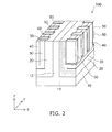
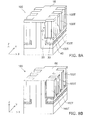
- FIG. 1 is a schematic perspective view illustrating the configuration of a semiconductor device according to a first embodiment.
- the semiconductor device 110 is a so-called 3D (three-dimensional) type in which the channel width of the MOSFET is provided along the depth direction of the substrate.
- the semiconductor device 110 includes a first semiconductor region 10, a second semiconductor region 20, a third semiconductor region 30, a fourth semiconductor region 40, a gate region 50, a gate insulating film 60, and an electric field relaxation region 70.
- the first semiconductor region 10 is a region of the first conductivity type including a first portion 11, which includes a first major surface 11a, and a second portion 12, which extends in a first direction orthogonal to the first major surface 11a.
- the first direction in which the second portion 12 extends is taken as a Z direction; one direction (a second direction) orthogonal to the first direction is taken as an X direction; and a third direction orthogonal to the first direction and the second direction is taken as a Y direction.
- the direction in which the second portion 12 extends along the Z direction is taken as "up”; and the direction opposite thereto is taken as "down".
- the first semiconductor region 10 is an n + drain region of, for example, a silicon wafer doped with phosphorus (P).
- the second semiconductor region 20 is a region of the first conductivity type including a third portion 23 and a fourth portion 24.
- the third portion 23 is provided on the first portion 11 with a length shorter than that of the second portion 12 along the Z direction.
- the fourth portion 24 is provided adjacent to the second portion 12 and extends in the Z direction from a portion of an upper face of the third portion 23.
- the second semiconductor region 20 is provided with a substantially L-shaped configuration along the first portion 11 and the second portion 12 in the cross-sectional view of the XZ plane by the third portion 23 and the fourth portion 24 being provided in directions orthogonal to each other.
- the second semiconductor region 20 is a film formed by, for example, epitaxial growth on the surface of the first semiconductor region 10.
- the second semiconductor region 20 is an n - drain region of, for example, an epitaxial film doped with phosphorus (P).
- P phosphorus
- the second semiconductor region 20 is used to form a drift region of the MOSFET.
- the third semiconductor region 30 is a region of the second conductivity type including a fifth portion 35 and a sixth portion 36.
- the fifth portion 35 is provided on the third portion 23 with a length shorter than that of the fourth portion 24 along the Z direction.
- the sixth portion 36 is provided adjacent to the fourth portion 24 and extends in the Z direction from a portion of an upper face of the fifth portion 35.
- the third semiconductor region 30 is provided with a substantially L-shaped configuration along the third portion 23 and the fourth portion 24 in the cross-sectional view of the XZ plane by the fifth portion 35 and the sixth portion 36 being provided in directions orthogonal to each other.
- a length h3 of the third semiconductor region 30 along the Z direction is shorter than a length h4 of the second semiconductor region 20 along the Z direction.
- the third semiconductor region 30 is a film formed by, for example, epitaxial growth on the surface of the second semiconductor region 20.
- the third semiconductor region 30 is a p - base region of, for example, an epitaxial film doped with boron (B).
- the fourth semiconductor region 40 is a region of the first conductivity type provided on the fifth portion 35 and adjacent to the sixth portion 36.
- the fourth semiconductor region 40 is provided on the third semiconductor region 30 and extends in the Z direction. Thereby, the fourth semiconductor region 40 is filled onto the inner side of the substantially L-shaped configuration of the third semiconductor region 30 in the cross-sectional view of the XZ plane.
- a length h2 of the fourth semiconductor region 40 along the Z direction is shorter than the length h3 of the third semiconductor region 30 along the Z direction.
- the fourth semiconductor region 40 is a film formed by, for example, epitaxial growth on the third semiconductor region 30.
- the fourth semiconductor region 40 is an n + source region of, for example, an epitaxial film doped with phosphorus (P).
- the gate region 50 is provided inside a trench 100T that pierces the second semiconductor region 20, the third semiconductor region 30, and the fourth semiconductor region 40 in the X direction.
- the fourth portion 24 of the second semiconductor region 20, the sixth portion 36 of the third semiconductor region 30, and the fourth semiconductor region 40 are adjacent along the X direction.
- the trench 100T is provided to pierce the adjacent fourth portion 24, sixth portion 36, and fourth semiconductor region 40 along the X direction.
- the gate region 50 is filled inside the trench 100T with the gate insulating film 60 described below interposed.
- the gate region 50 is provided inside the trench 100T and extends along the Z direction.
- the gate region 50 is provided with a length h1 along the Z direction.
- the length h1 is, for example, shorter than the length h2 of the fourth semiconductor region 40.
- Polycrystalline silicon for example, may be used as the gate region 50.
- the gate insulating film 60 is provided between the gate region 50 and an inner wall of the trench 100T.
- a silicon oxide film for example, may be used as the gate insulating film 60.
- the electric field relaxation region 70 is provided between the third portion 23 of the second semiconductor region 20 and the fifth portion 35 of the third semiconductor region 30.
- the electric field relaxation region 70 is a region of the second conductivity type having an impurity concentration lower than the impurity concentration of the third semiconductor region 30.
- the electric field relaxation region 70 is a p - region of, for example, the third portion 23 doped with boron (B).
- the electric field relaxation region 70 is provided from between the third portion 23 and the fifth portion 35 to a portion of the fourth portion 24.
- the electric field relaxation region 70 is provided around the outer side of the corner of the substantially L-shaped configuration of the third semiconductor region 30 in the cross-sectional view of the XZ plane.
- an abrupt impurity concentration change between the p - -type third semiconductor region 30 and the n - -type second semiconductor region 20 is relaxed.
- the electric field relaxation region 70 functions as a RESURF region to relax the electric field concentration around the corner of the substantially L-shaped configuration of the third semiconductor region 30.
- a channel is formed in the p- base region which is the third semiconductor region 30 adjacent to the gate insulating film 60 by applying an on-voltage to the gate region 50.
- the length of the third semiconductor region 30 along the X direction corresponds to the channel length.
- the depth h1 corresponding to the gate region 50 is the portion of the length of the third semiconductor region 30 along the Z direction that corresponds to the channel width.
- the channel is not formed in the p- base region which is the third semiconductor region 30; and the current does not flow. Because the electric field relaxation region 70 is provided between the third semiconductor region 30 and the second semiconductor region 20 in the semiconductor device 110 according to the embodiment, a depletion layer reaches the electric field relaxation region 70 from the channel region. Thereby, the electric field concentration around the corner of the third semiconductor region 30 is relaxed; and the breakdown voltage can be increased.
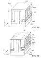
- FIG. 2 is a schematic perspective view illustrating a semiconductor device according to a reference example.
- the semiconductor device 190 does not include an electric field relaxation region 70 such as that of the semiconductor device 110 illustrated in FIG. 1 .
- FIG. 2 illustrates the electric field applied between the third semiconductor region 30 and the second semiconductor region 20 when the MOSFET is in the off-state.
- the electric field concentrates around the corner of the third semiconductor region 30.
- the first portion 11 and the second portion 12 of the first semiconductor region 10 are provided around two faces of the second semiconductor region 20 (the XY plane and the YZ plane).
- the third semiconductor region 30 is provided on inner sides of the second semiconductor region 20. Therefore, the third semiconductor region 30 contacts the second semiconductor region 20 at two orthogonal faces (the XY plane and the YZ plane). Thereby, the electric field concentrates easily at the corner of the third semiconductor region 30 between the two faces recited above.
- the region from the fifth portion 35 of the third semiconductor region 30 toward the first portion 11 of the first semiconductor region 10 is equivalent to the terminal region of a so-called 3D-MOSFET. Therefore, the electric field concentrating around the corner of the third semiconductor region 30 between the two faces recited above is equivalent to a decrease of the breakdown voltage in the terminal region, which leads to a decrease of the breakdown voltage of the entire semiconductor device 190.
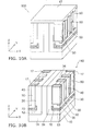
- FIG. 3 is a schematic perspective view illustrating the state of the electric field of the semiconductor device 110 according to the embodiment.
- FIG. 3 illustrate the electric field applied between the third semiconductor region 30 and the second semiconductor region 20 when the MOSFET of the semiconductor device 110 according to the embodiment is in the off-state.
- the semiconductor device 110 includes the electric field relaxation region 70 as described above, the electric field concentration between the third semiconductor region 30 and the second semiconductor region 20 is relaxed particularly around the corner of the third semiconductor region 30. Thereby, the breakdown voltage in the terminal region can be higher and the breakdown voltage of the entire semiconductor device 110 can be higher than those of the semiconductor device 190 according to the reference example illustrated in FIG. 2 .
- the second portion 12 of the first semiconductor region 10 is provided extending along the Y direction.
- the third semiconductor region 30 and the fourth semiconductor region 40 extend along the Y direction.
- multiple gate regions 50 and multiple gate insulating films 60 are disposed along the Y direction.
- multiple MOSFET structures are provided corresponding to the second portion 12 extending in the Y direction.
- the gate regions of the multiple MOSFET structures are connected, for example, in parallel.
- the source regions of the multiple MOSFET structures are connected, for example, in parallel.
- the second semiconductor region 20, the third semiconductor region 30, the fourth semiconductor region, the multiple gate regions 50, and the multiple gate insulating films 60 are provided on both X-direction sides of the second portion 12.
- multiple second portions 12 may be disposed along the X direction; and these may include the multiple MOSFET structures provided on both X-direction sides of each of the second portions 12.
- the breakdown voltage can be increased by the electric field concentration being relaxed around the corner of the third semiconductor region 30.
- the second embodiment is a method for manufacturing the semiconductor device according to the first embodiment.
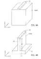
- FIG. 4A to FIG. 10B are schematic perspective views illustrating the method for manufacturing the semiconductor device according to the first embodiment.
- a wafer 10W of, for example, silicon is prepared.
- the wafer 10W is doped with, for example, phosphorus (P) to form the drain region which is the first semiconductor region 10; and the wafer 10W is n + .
- the impurity concentration of the wafer 10W is, for example, 4.5x 10 19 cm -3 .
- a silicon oxide film 15 is formed on the wafer 10W and patterned using photolithography and etching. Only the portion of the silicon oxide film 15 used to form the second portion 12 described below remains after the patterning.
- the wafer 10W is etched using the patterned silicon oxide film 15 as a mask.
- the etching is performed using, for example, RIE (Reactive Ion Etching).
- RIE Reactive Ion Etching
- the etched portion of the wafer 10W remaining after the etching becomes the first portion 11.
- the portion masked by the silicon oxide film 15 and not etched becomes the second portion 12.
- the first semiconductor region 10 including the first portion 11 and the second portion 12 is formed.
- the etching depth of the wafer 10W is, for example, 15 micrometers ( ⁇ m) to 20 ⁇ m.
- a length h5 of the second portion 12 along the Z direction is 15 ⁇ m to 20 ⁇ m.
- the silicon oxide film 15 is removed.
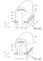
- the second semiconductor region 20 is formed as a film on the surface of the first semiconductor region 10.
- the second semiconductor region 20 is formed by, for example, epitaxial growth on the surface of the first semiconductor region 10.
- the second semiconductor region 20 is formed with a thickness of about 2 ⁇ m by the epitaxial growth.
- the second semiconductor region 20 is formed to cover the surfaces of the first portion 11 and the second portion 12 of the first semiconductor region 10. Thereby, the third portion 23 is formed on the first portion 11; and the fourth portion 24 is formed adjacent to the second portion 12.
- the second semiconductor region 20 is doped with, for example, phosphorus (P). Thereby, the second semiconductor region 20 becomes an n- drain region.
- the impurity concentration of the second semiconductor region 20 is, for example, 2 ⁇ 10 16 cm -3 .
- ion implantation is performed from above the second semiconductor region 20.
- the ion implantation implants, for example, boron (B) ions as the impurity such that the second semiconductor region 20 is p - .
- the boron (B) ions are implanted into an upper face 20c of the second semiconductor region 20 and a second major surface 20a of the second semiconductor region 20 opposing a first major surface 10a of the first semiconductor region 10.
- the p- region due to the boron (B) implanted into the second major surface 20a becomes the electric field relaxation region 70.
- the impurity concentration of the p- region (the electric field relaxation region 70) is lower than the impurity concentration of the third semiconductor region 30 formed subsequently.
- the boron is implanted with a dose of 1 ⁇ 10 14 cm -2 .
- the impurity concentration of the p - region (the electric field relaxation region 70) is less than 1 ⁇ 10 18 cm -3 .
- the incident angle of the ions of the ion implantation is an angle at which the ions are implanted into the second major surface 20a of the second semiconductor region 20 but are not implanted into a third major surface 20b of the second semiconductor region 20 opposing the side face of the second portion 12.
- the incident angle of the ions is, for example, about 3 degrees from a direction perpendicular to the second major surface 20a.
- the impurity is diffused by heat treatment.
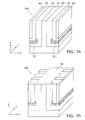
- the third semiconductor region 30 is formed as a film on the surface of the second semiconductor region 20.
- the third semiconductor region 30 is formed on the surface of the second semiconductor region 20 by, for example, epitaxial growth.
- the third semiconductor region 30 is formed with a thickness of about 0.35 ⁇ m by the epitaxial growth.
- the fifth portion 35 is formed on the third portion 23; and the sixth portion 36 is formed adjacent to the fourth portion 24.
- the third semiconductor region 30 is doped with, for example, boron (B) to become the p- base region.
- the impurity concentration of the third semiconductor region 30 is, for example, 1 ⁇ 10 18 cm -3 . In other words, the impurity concentration is higher than the impurity concentration of the electric field relaxation region 70 formed previously.
- the fourth semiconductor region 40 is formed as a film on the surface of the third semiconductor region 30.
- the fourth semiconductor region 40 is formed on the surface of the third semiconductor region 30 by, for example, epitaxial growth.
- the fourth semiconductor region 40 is formed with a thickness of about 0.55 ⁇ m by the epitaxial growth. Thereby, the fourth semiconductor region 40 is provided on the fifth portion 35 and adjacent to the sixth portion 36.
- the fourth semiconductor region 40 is doped with, for example, phosphorus (P) to become the n + source region.
- the impurity concentration of the fourth semiconductor region 40 is, for example, 3 ⁇ 10 19 cm -3 .
- the removal method may include, for example, CMP (Chemical Mechanical Polishing).
- CMP Chemical Mechanical Polishing
- a structural body 100, in which the exposed surface of the second portion 12 is planarized, is formed by the CMP.
- a mask material 16 is formed on the structural body 100.
- the mask material 16 may include, for example, silicon oxide.
- the mask material 16 is formed using, for example, CVD (Chemical Vapor Deposition).
- patterning of the mask material 16 is performed using photolithography and etching.
- a resist (not illustrated) is coated onto the mask material 16 and patterned using photolithography and etching.
- the mask material 16 is etched and patterned by, for example, RIE using the resist as a mask. In the patterning, openings are made in the mask material 16 only in the portions where the gate region 50 and the gate insulating film 60 are to be formed.
- the resist is removed.
- the structural body 100 is etched using the patterned mask material 16 as a mask. By this etching, the structural body 100 at the opening portion of the mask material 16 is carved to make the trench 100T.
- the trench 100T is provided to pierce the second semiconductor region 20, the third semiconductor region 30, and the fourth semiconductor region 40 along the X direction.
- the trench 100T is made with a width of about 1 ⁇ m along the Y direction and a length ht1 of about 15 ⁇ m to 20 ⁇ m along the Z direction. In the embodiment, the length ht1 of the trench 100T along the Z direction is shorter than the length h2 of the fourth semiconductor region 40 along the Z direction. Multiple trenches 100T may be provided along the Y direction and the X direction as necessary.
- the mask material 16 is removed.
- the gate insulating film 60 is formed on the structural body 100 in which the trench 100T is made.
- the gate insulating film 60 is, for example, a silicon oxide film.
- the silicon oxide film may be formed by, for example, thermal oxidation.
- the gate insulating film 60 is formed with a thickness of, for example, 100 nanometers (nm).
- a gate material 50A is formed on the gate insulating film 60.
- the gate material 50A is, for example, polycrystalline silicon.
- the gate material 50A is filled onto the upper face of the structural body 100 and into the trench 100T.
- etch-back of the gate material 50A is performed. Thereby, as illustrated in FIG. 9B , the gate region 50 is provided inside the trench 100T with the gate insulating film 60 interposed.
- the upper face of the gate region 50 formed by the etch-back of the gate material 50A is slightly lower than the opening of the trench 100T along the Z direction.
- an inter-layer insulating film 17 is formed on the structural body 100.
- the inter-layer insulating film 17 is formed on the entire surface of the upper face of the structural body 100.
- the inter-layer insulating film 17 is etched using, for example, RIE. This etching is performed until the second portion 12, the second semiconductor region 20, the third semiconductor region 30, and the fourth semiconductor region 40 are exposed as illustrated in FIG. 10B . Thereby, the inter-layer insulating film 17 remains on the gate region 50.
- not-illustrated electrodes are formed to be electrically connected to the gate region 50, the drain region which is the first semiconductor region 10, and the source region which is the fourth semiconductor region 40.
- the electrodes may include, for example, aluminum (Al).
- Al aluminum
- the electrodes undergo the prescribed patterning using photolithography and etching.
- a protective film such as, for example, polyimide is formed. Thereby, the semiconductor device 110 is completed.
- the electric field relaxation region 70 is included between the third semiconductor region 30 and the second semiconductor region 20; and it is possible to manufacture the semiconductor device 110 having a relaxed electric field concentration and a higher breakdown voltage.
- the first conductivity type is the n type and the second conductivity type is the p type in the description of the embodiments described above, the invention is practicable also when the first conductivity type is the p type and the second conductivity type is the n type.
- a MOSFET using silicon (Si) as the semiconductor is described in the embodiments described above, a compound semiconductor such as, for example, silicon carbide (SiC) or gallium nitride (GaN) or a wide bandgap semiconductor such as diamond may be used as the semiconductor.
- the semiconductor device may be, for example, a device combining a MOSFET and a SBD (Schottky Barrier Diode) or a device such as an IGBT (Insulated Gate Bipolar Transistor).
- SBD Schottky Barrier Diode
- IGBT Insulated Gate Bipolar Transistor
- the breakdown voltage of the semiconductor device can be increased.
Abstract
A semiconductor device (110) includes a first semiconductor region (10), a second semiconductor region (20), a third semiconductor region (30), a fourth semiconductor region (40), a gate region (50), a gate insulating film (60), and an electric field relaxation region (70). The first semiconductor regian (10) includes a first portion (11) and a second portion (12), the first portion having a first major surface (11a), the second portion extending in a first direction orthogonal to the first major surface. The second semiconductor region (20) includes a third portion (23) and a fourth portion (24) adjacent to the second portion. The third semiconductor region (30) includes a fifth portion (35) and a sixth portion (36) adjacent to the fourth portion. The fourth semiconductor region (40) is adjacent to the sixth portion (36). The gate region (50) is provided inside a trench (100T) made in a second direction orthogonal to the first direction. The gate insulating film (60) is provided between the gate region (50) and an inner wall of the trench (100T). The electric field relaxation region (70) is provided between the third portion (23) and the fifth portion (35) and has an impurity concentration lower than an impurity concentration of the third semiconductor region (30).
Description
- Embodiments described herein relate generally to a semiconductor device and a method for manufacturing the same.
- Conventionally, planar MOSFETs and trench MOSFETs have been employed as structures of, for example, a power MOSFET (Metal-Oxide-Semiconductor Field Effect Transistor). Also, a so-called 3D MOSFET, in which the channel width of the MOSFET is provided in the depth direction of the substrate, has been considered. However, further improvement of the breakdown voltage is desirable for so-called 3D MOSFETs.
-
-
FIG. 1 is a schematic perspective view illustrating the configuration of a semiconductor device according to an embodiment; -
FIG. 2 is a schematic perspective view illustrating a semiconductor device according to a reference example; -
FIG. 3 is a schematic perspective view illustrating the state of the electric field of the semiconductor device according to the embodiment; and -
FIG. 4A to FIG. 10B are schematic perspective views illustrating a method for manufacturing the semiconductor device according to the embodiment. - According to one embodiment, a semiconductor device includes a first semiconductor region of a first conductivity type, a second semiconductor region of the first conductivity type, a third semiconductor region of a second conductivity type, a fourth semiconductor region of the first conductivity type, a gate region, a gate insulating film, and an electric field relaxation region of the second conductivity type. The first semiconductor region includes a first portion and a second portion. The first portion has a first major surface. The second portion extends in a first direction orthogonal to the first major surface. The second semiconductor region includes a third portion and a fourth portion. The third portion is provided on the first portion side and has a length shorter than a length of the second portion along the first direction. The fourth portion is adjacent to the second portion and extends in the first direction from a portion of an upper face of the third portion. The third semiconductor region includes a fifth portion and a sixth portion. The fifth portion is provided on the third portion side and has a length shorter than a length of the fourth portion along the first direction. The sixth portion is adjacent to the fourth portion and extends in the first direction from a portion of an upper face of the fifth portion. The fourth semiconductor region is provided on the fifth portion and adjacent to the sixth portion. The gate region is provided inside a trench made in a second direction orthogonal to the first direction in the second semiconductor region, the third semiconductor region, and the fourth semiconductor region. The gate insulating film is provided between the gate region and an inner wall of the trench. The electric field relaxation region is provided between the third portion and the fifth portion. The electric field relaxation region has an impurity concentration lower than an impurity concentration of the third semiconductor region.
- According to another embodiment, a method is disclosed for manufacturing a semiconductor device. The method can include forming a first semiconductor region of a first conductivity type including a first portion and a second portion. The first portion has a first major surface. The second portion extends in a first direction orthogonal to the first major surface. The method can include covering the first semiconductor region with a second semiconductor region of the first conductivity type to form a third portion and a fourth portion. The third portion is provided on the first portion side and has a length shorter than a length of the second portion along the first direction. The fourth portion is adjacent to the second portion and extends in the first direction from a portion of an upper face of the third portion. The method can include forming an electric field relaxation region of a second conductivity type in a second major surface of the third portion. The second major surface opposes the first major surface. The method can include covering the second semiconductor region with a third semiconductor region of the second conductivity type to form a fifth portion and a sixth portion. The fifth portion is provided on the third portion side and has a length shorter than a length of the fourth portion along the first direction. The sixth portion is adjacent to the fourth portion and extends in the first direction from a portion of an upper face of the fifth portion. The method can include covering the third semiconductor region with a fourth semiconductor region of the first conductivity type. The method can include removing the fourth semiconductor region, the third semiconductor region, and the second semiconductor region until the second portion is exposed. In addition, the method can include making a trench in a second direction orthogonal to the first direction in the second semiconductor region, the third semiconductor region, and the fourth semiconductor region and forming a gate region inside the trench with a gate insulating film interposed.
- Embodiments of the invention will now be described based on the drawings.
- The drawings are schematic or conceptual; and the relationships between the thicknesses and widths of portions, the proportional coefficients of sizes among portions, etc., are not necessarily the same as the actual values thereof. Further, the dimensions and the proportional coefficients may be illustrated differently among the drawings, even for identical portions.
- In the specification and the drawings of the application, components similar to those described in regard to a drawing thereinabove are marked with like reference numerals, and a detailed description is omitted as appropriate.
- In the description hereinbelow, specific examples are illustrated in which silicon (Si) is used as an example of a semiconductor, a first conductivity type is an n type, and a second conductivity type is a p type. In the description hereinbelow, the notations of n+, n, n-, p+, p, and p- indicate relative degrees of the impurity concentration of each of the conductivity types. In other words, n+ is an n-type impurity concentration relatively higher than n; and n- is an n-type impurity concentration relatively lower than n. Also, p+ is a p-type impurity concentration relatively higher than p; and p- is a p-type impurity concentration relatively lower than p.
-
FIG. 1 is a schematic perspective view illustrating the configuration of a semiconductor device according to a first embodiment. - As illustrated in
FIG. 1 , thesemiconductor device 110 according to the embodiment is a so-called 3D (three-dimensional) type in which the channel width of the MOSFET is provided along the depth direction of the substrate. - The
semiconductor device 110 includes afirst semiconductor region 10, asecond semiconductor region 20, athird semiconductor region 30, afourth semiconductor region 40, agate region 50, agate insulating film 60, and an electricfield relaxation region 70. - The
first semiconductor region 10 is a region of the first conductivity type including afirst portion 11, which includes a firstmajor surface 11a, and asecond portion 12, which extends in a first direction orthogonal to the firstmajor surface 11a. - In the embodiment, the first direction in which the
second portion 12 extends is taken as a Z direction; one direction (a second direction) orthogonal to the first direction is taken as an X direction; and a third direction orthogonal to the first direction and the second direction is taken as a Y direction. For convenience of description in the embodiment, the direction in which thesecond portion 12 extends along the Z direction is taken as "up"; and the direction opposite thereto is taken as "down". - In the embodiment, the
first semiconductor region 10 is an n+ drain region of, for example, a silicon wafer doped with phosphorus (P). - The
second semiconductor region 20 is a region of the first conductivity type including athird portion 23 and afourth portion 24. - The
third portion 23 is provided on thefirst portion 11 with a length shorter than that of thesecond portion 12 along the Z direction. Thefourth portion 24 is provided adjacent to thesecond portion 12 and extends in the Z direction from a portion of an upper face of thethird portion 23. - In other words, the
second semiconductor region 20 is provided with a substantially L-shaped configuration along thefirst portion 11 and thesecond portion 12 in the cross-sectional view of the XZ plane by thethird portion 23 and thefourth portion 24 being provided in directions orthogonal to each other. - In the embodiment, the
second semiconductor region 20 is a film formed by, for example, epitaxial growth on the surface of thefirst semiconductor region 10. Thesecond semiconductor region 20 is an n- drain region of, for example, an epitaxial film doped with phosphorus (P). Thesecond semiconductor region 20 is used to form a drift region of the MOSFET. - The
third semiconductor region 30 is a region of the second conductivity type including afifth portion 35 and asixth portion 36. - The
fifth portion 35 is provided on thethird portion 23 with a length shorter than that of thefourth portion 24 along the Z direction. Thesixth portion 36 is provided adjacent to thefourth portion 24 and extends in the Z direction from a portion of an upper face of thefifth portion 35. - In other words, the
third semiconductor region 30 is provided with a substantially L-shaped configuration along thethird portion 23 and thefourth portion 24 in the cross-sectional view of the XZ plane by thefifth portion 35 and thesixth portion 36 being provided in directions orthogonal to each other. - A length h3 of the
third semiconductor region 30 along the Z direction is shorter than a length h4 of thesecond semiconductor region 20 along the Z direction. - In the embodiment, the
third semiconductor region 30 is a film formed by, for example, epitaxial growth on the surface of thesecond semiconductor region 20. Thethird semiconductor region 30 is a p- base region of, for example, an epitaxial film doped with boron (B). - The
fourth semiconductor region 40 is a region of the first conductivity type provided on thefifth portion 35 and adjacent to thesixth portion 36. - In other words, the
fourth semiconductor region 40 is provided on thethird semiconductor region 30 and extends in the Z direction. Thereby, thefourth semiconductor region 40 is filled onto the inner side of the substantially L-shaped configuration of thethird semiconductor region 30 in the cross-sectional view of the XZ plane. - A length h2 of the
fourth semiconductor region 40 along the Z direction is shorter than the length h3 of thethird semiconductor region 30 along the Z direction. - In the embodiment, the
fourth semiconductor region 40 is a film formed by, for example, epitaxial growth on thethird semiconductor region 30. Thefourth semiconductor region 40 is an n+ source region of, for example, an epitaxial film doped with phosphorus (P). - The
gate region 50 is provided inside atrench 100T that pierces thesecond semiconductor region 20, thethird semiconductor region 30, and thefourth semiconductor region 40 in the X direction. - In other words, the
fourth portion 24 of thesecond semiconductor region 20, thesixth portion 36 of thethird semiconductor region 30, and thefourth semiconductor region 40 are adjacent along the X direction. Thetrench 100T is provided to pierce the adjacentfourth portion 24,sixth portion 36, andfourth semiconductor region 40 along the X direction. Thegate region 50 is filled inside thetrench 100T with thegate insulating film 60 described below interposed. - The
gate region 50 is provided inside thetrench 100T and extends along the Z direction. Thegate region 50 is provided with a length h1 along the Z direction. The length h1 is, for example, shorter than the length h2 of thefourth semiconductor region 40. Polycrystalline silicon, for example, may be used as thegate region 50. - The
gate insulating film 60 is provided between thegate region 50 and an inner wall of thetrench 100T. A silicon oxide film, for example, may be used as thegate insulating film 60. - The electric
field relaxation region 70 is provided between thethird portion 23 of thesecond semiconductor region 20 and thefifth portion 35 of thethird semiconductor region 30. The electricfield relaxation region 70 is a region of the second conductivity type having an impurity concentration lower than the impurity concentration of thethird semiconductor region 30. The electricfield relaxation region 70 is a p- region of, for example, thethird portion 23 doped with boron (B). - The electric
field relaxation region 70 is provided from between thethird portion 23 and thefifth portion 35 to a portion of thefourth portion 24. In other words, the electricfield relaxation region 70 is provided around the outer side of the corner of the substantially L-shaped configuration of thethird semiconductor region 30 in the cross-sectional view of the XZ plane. In the case where such an electricfield relaxation region 70 is provided, an abrupt impurity concentration change between the p--typethird semiconductor region 30 and the n--typesecond semiconductor region 20 is relaxed. In other words, in thesemiconductor device 110 according to the embodiment, the electricfield relaxation region 70 functions as a RESURF region to relax the electric field concentration around the corner of the substantially L-shaped configuration of thethird semiconductor region 30. - In the
semiconductor device 110 according to the embodiment, a channel is formed in the p- base region which is thethird semiconductor region 30 adjacent to thegate insulating film 60 by applying an on-voltage to thegate region 50. In thesemiconductor device 110, the length of thethird semiconductor region 30 along the X direction corresponds to the channel length. In thesemiconductor device 110, the depth h1 corresponding to thegate region 50 is the portion of the length of thethird semiconductor region 30 along the Z direction that corresponds to the channel width. When the channel is formed in the entirethird semiconductor region 30 in the channel length direction, a current flows from thefourth semiconductor region 40 which is the source region via thesecond semiconductor region 20 which is the drift region to thefirst semiconductor region 10 which is the drain region. - On the other hand, in the state in which the on-voltage is not applied to the
gate region 50, the channel is not formed in the p- base region which is thethird semiconductor region 30; and the current does not flow. Because the electricfield relaxation region 70 is provided between thethird semiconductor region 30 and thesecond semiconductor region 20 in thesemiconductor device 110 according to the embodiment, a depletion layer reaches the electricfield relaxation region 70 from the channel region. Thereby, the electric field concentration around the corner of thethird semiconductor region 30 is relaxed; and the breakdown voltage can be increased. -
FIG. 2 is a schematic perspective view illustrating a semiconductor device according to a reference example. - As illustrated in
FIG. 2 , thesemiconductor device 190 according to the reference example does not include an electricfield relaxation region 70 such as that of thesemiconductor device 110 illustrated inFIG. 1 . - The broken lines of
FIG. 2 illustrate the electric field applied between thethird semiconductor region 30 and thesecond semiconductor region 20 when the MOSFET is in the off-state. In thesemiconductor device 190, the electric field concentrates around the corner of thethird semiconductor region 30. - In the
semiconductor device 190, thefirst portion 11 and thesecond portion 12 of thefirst semiconductor region 10 are provided around two faces of the second semiconductor region 20 (the XY plane and the YZ plane). Thethird semiconductor region 30 is provided on inner sides of thesecond semiconductor region 20. Therefore, thethird semiconductor region 30 contacts thesecond semiconductor region 20 at two orthogonal faces (the XY plane and the YZ plane). Thereby, the electric field concentrates easily at the corner of thethird semiconductor region 30 between the two faces recited above. - It may be considered that the region from the
fifth portion 35 of thethird semiconductor region 30 toward thefirst portion 11 of thefirst semiconductor region 10 is equivalent to the terminal region of a so-called 3D-MOSFET. Therefore, the electric field concentrating around the corner of thethird semiconductor region 30 between the two faces recited above is equivalent to a decrease of the breakdown voltage in the terminal region, which leads to a decrease of the breakdown voltage of theentire semiconductor device 190. -
FIG. 3 is a schematic perspective view illustrating the state of the electric field of thesemiconductor device 110 according to the embodiment. - The broken lines of
FIG. 3 illustrate the electric field applied between thethird semiconductor region 30 and thesecond semiconductor region 20 when the MOSFET of thesemiconductor device 110 according to the embodiment is in the off-state. - Because the
semiconductor device 110 according to the embodiment includes the electricfield relaxation region 70 as described above, the electric field concentration between thethird semiconductor region 30 and thesecond semiconductor region 20 is relaxed particularly around the corner of thethird semiconductor region 30. Thereby, the breakdown voltage in the terminal region can be higher and the breakdown voltage of theentire semiconductor device 110 can be higher than those of thesemiconductor device 190 according to the reference example illustrated inFIG. 2 . - In the
semiconductor device 110 illustrated inFIG. 1 , thesecond portion 12 of thefirst semiconductor region 10 is provided extending along the Y direction. In thesemiconductor device 110, thethird semiconductor region 30 and thefourth semiconductor region 40 extend along the Y direction. In thesemiconductor device 110,multiple gate regions 50 and multiplegate insulating films 60 are disposed along the Y direction. - Thereby, multiple MOSFET structures are provided corresponding to the
second portion 12 extending in the Y direction. The gate regions of the multiple MOSFET structures are connected, for example, in parallel. The source regions of the multiple MOSFET structures are connected, for example, in parallel. - In the
semiconductor device 110 illustrated inFIG. 1 , thesecond semiconductor region 20, thethird semiconductor region 30, the fourth semiconductor region, themultiple gate regions 50, and the multiplegate insulating films 60 are provided on both X-direction sides of thesecond portion 12. - In the
semiconductor device 110, multiplesecond portions 12 may be disposed along the X direction; and these may include the multiple MOSFET structures provided on both X-direction sides of each of thesecond portions 12. - In such a
semiconductor device 110 according to the embodiment, the breakdown voltage can be increased by the electric field concentration being relaxed around the corner of thethird semiconductor region 30. - A second embodiment will now be described. The second embodiment is a method for manufacturing the semiconductor device according to the first embodiment.
-
FIG. 4A to FIG. 10B are schematic perspective views illustrating the method for manufacturing the semiconductor device according to the first embodiment. - First, as illustrated in
FIG. 4A , a wafer 10W of, for example, silicon is prepared. The wafer 10W is doped with, for example, phosphorus (P) to form the drain region which is thefirst semiconductor region 10; and the wafer 10W is n+. The impurity concentration of the wafer 10W is, for example, 4.5x 1019 cm-3 . - Then, for example, a
silicon oxide film 15 is formed on the wafer 10W and patterned using photolithography and etching. Only the portion of thesilicon oxide film 15 used to form thesecond portion 12 described below remains after the patterning. - Then, as illustrated in
FIG. 4B , the wafer 10W is etched using the patternedsilicon oxide film 15 as a mask. The etching is performed using, for example, RIE (Reactive Ion Etching). The etched portion of the wafer 10W remaining after the etching becomes thefirst portion 11. The portion masked by thesilicon oxide film 15 and not etched becomes thesecond portion 12. Thereby, thefirst semiconductor region 10 including thefirst portion 11 and thesecond portion 12 is formed. - Here, the etching depth of the wafer 10W is, for example, 15 micrometers (µm) to 20 µm. Thereby, a length h5 of the
second portion 12 along the Z direction is 15 µm to 20 µm. - After the wafer 10W is etched, the
silicon oxide film 15 is removed. - Then, as illustrated in
FIG. 5A , thesecond semiconductor region 20 is formed as a film on the surface of thefirst semiconductor region 10. Thesecond semiconductor region 20 is formed by, for example, epitaxial growth on the surface of thefirst semiconductor region 10. Thesecond semiconductor region 20 is formed with a thickness of about 2 µm by the epitaxial growth. Thesecond semiconductor region 20 is formed to cover the surfaces of thefirst portion 11 and thesecond portion 12 of thefirst semiconductor region 10. Thereby, thethird portion 23 is formed on thefirst portion 11; and thefourth portion 24 is formed adjacent to thesecond portion 12. - After the epitaxial growth, the
second semiconductor region 20 is doped with, for example, phosphorus (P). Thereby, thesecond semiconductor region 20 becomes an n- drain region. The impurity concentration of thesecond semiconductor region 20 is, for example, 2×1016 cm-3. - Then, as illustrated in
FIG. 5B , ion implantation is performed from above thesecond semiconductor region 20. The ion implantation implants, for example, boron (B) ions as the impurity such that thesecond semiconductor region 20 is p-. Here, the boron (B) ions are implanted into anupper face 20c of thesecond semiconductor region 20 and a secondmajor surface 20a of thesecond semiconductor region 20 opposing a first major surface 10a of thefirst semiconductor region 10. Thereof, the p- region due to the boron (B) implanted into the secondmajor surface 20a becomes the electricfield relaxation region 70. - The impurity concentration of the p- region (the electric field relaxation region 70) is lower than the impurity concentration of the
third semiconductor region 30 formed subsequently. Here, for example, the boron is implanted with a dose of 1×1014 cm-2. Thereby, the impurity concentration of the p- region (the electric field relaxation region 70) is less than 1 × 1018 cm-3. - The incident angle of the ions of the ion implantation is an angle at which the ions are implanted into the second
major surface 20a of thesecond semiconductor region 20 but are not implanted into a thirdmajor surface 20b of thesecond semiconductor region 20 opposing the side face of thesecond portion 12. The incident angle of the ions is, for example, about 3 degrees from a direction perpendicular to the secondmajor surface 20a. Thereby, the ions that bombard the thirdmajor surface 20b of thesecond semiconductor region 20 are repelled; and the ions are implanted into the secondmajor surface 20a without being implanted into the thirdmajor surface 20b. Although the impurity is implanted into theupper face 20c as well, this is removed by polishing in a subsequent process. - After implanting the impurity into the
second semiconductor region 20, the impurity is diffused by heat treatment. - Then, as illustrated in
FIG. 6A , thethird semiconductor region 30 is formed as a film on the surface of thesecond semiconductor region 20. Thethird semiconductor region 30 is formed on the surface of thesecond semiconductor region 20 by, for example, epitaxial growth. Thethird semiconductor region 30 is formed with a thickness of about 0.35 µm by the epitaxial growth. Thereby, thefifth portion 35 is formed on thethird portion 23; and thesixth portion 36 is formed adjacent to thefourth portion 24. - After the epitaxial growth, the
third semiconductor region 30 is doped with, for example, boron (B) to become the p- base region. The impurity concentration of thethird semiconductor region 30 is, for example, 1 × 1018 cm-3. In other words, the impurity concentration is higher than the impurity concentration of the electricfield relaxation region 70 formed previously. - Then, as illustrated in
FIG. 6B , thefourth semiconductor region 40 is formed as a film on the surface of thethird semiconductor region 30. Thefourth semiconductor region 40 is formed on the surface of thethird semiconductor region 30 by, for example, epitaxial growth. Thefourth semiconductor region 40 is formed with a thickness of about 0.55 µm by the epitaxial growth. Thereby, thefourth semiconductor region 40 is provided on thefifth portion 35 and adjacent to thesixth portion 36. - After the epitaxial growth, the
fourth semiconductor region 40 is doped with, for example, phosphorus (P) to become the n+ source region. The impurity concentration of thefourth semiconductor region 40 is, for example, 3 × 1019 cm-3. - Then, as illustrated in
FIG. 7A , thefourth semiconductor region 40, thethird semiconductor region 30, and thesecond semiconductor region 20 are removed until thesecond portion 12 of thefirst semiconductor region 10 is exposed. The removal method may include, for example, CMP (Chemical Mechanical Polishing). Astructural body 100, in which the exposed surface of thesecond portion 12 is planarized, is formed by the CMP. - Continuing as illustrated in
FIG. 7B , amask material 16 is formed on thestructural body 100. Themask material 16 may include, for example, silicon oxide. Themask material 16 is formed using, for example, CVD (Chemical Vapor Deposition). After forming themask material 16, patterning of themask material 16 is performed using photolithography and etching. For example, a resist (not illustrated) is coated onto themask material 16 and patterned using photolithography and etching. Subsequently, themask material 16 is etched and patterned by, for example, RIE using the resist as a mask. In the patterning, openings are made in themask material 16 only in the portions where thegate region 50 and thegate insulating film 60 are to be formed. After the patterning of themask material 16, the resist is removed. - Then, as illustrated in
FIG. 8A , thestructural body 100 is etched using the patternedmask material 16 as a mask. By this etching, thestructural body 100 at the opening portion of themask material 16 is carved to make thetrench 100T. Thetrench 100T is provided to pierce thesecond semiconductor region 20, thethird semiconductor region 30, and thefourth semiconductor region 40 along the X direction. Thetrench 100T is made with a width of about 1 µm along the Y direction and a length ht1 of about 15 µm to 20 µm along the Z direction. In the embodiment, the length ht1 of thetrench 100T along the Z direction is shorter than the length h2 of thefourth semiconductor region 40 along the Z direction.Multiple trenches 100T may be provided along the Y direction and the X direction as necessary. - After making the
trench 100T, themask material 16 is removed. - Then, as illustrated in
FIG. 8B , thegate insulating film 60 is formed on thestructural body 100 in which thetrench 100T is made. Thegate insulating film 60 is, for example, a silicon oxide film. The silicon oxide film may be formed by, for example, thermal oxidation. Thegate insulating film 60 is formed with a thickness of, for example, 100 nanometers (nm). - Continuing as illustrated in
FIG. 9A , agate material 50A is formed on thegate insulating film 60. Thegate material 50A is, for example, polycrystalline silicon. Thegate material 50A is filled onto the upper face of thestructural body 100 and into thetrench 100T. - Then, etch-back of the
gate material 50A is performed. Thereby, as illustrated inFIG. 9B , thegate region 50 is provided inside thetrench 100T with thegate insulating film 60 interposed. The upper face of thegate region 50 formed by the etch-back of thegate material 50A is slightly lower than the opening of thetrench 100T along the Z direction. - Continuing as illustrated in
FIG. 10A , an inter-layerinsulating film 17 is formed on thestructural body 100. The inter-layerinsulating film 17 is formed on the entire surface of the upper face of thestructural body 100. Subsequently, the inter-layer insulatingfilm 17 is etched using, for example, RIE. This etching is performed until thesecond portion 12, thesecond semiconductor region 20, thethird semiconductor region 30, and thefourth semiconductor region 40 are exposed as illustrated inFIG. 10B . Thereby, the inter-layer insulatingfilm 17 remains on thegate region 50. - Subsequently, not-illustrated electrodes (the gate electrode, the drain electrode, and the source electrode) are formed to be electrically connected to the
gate region 50, the drain region which is thefirst semiconductor region 10, and the source region which is thefourth semiconductor region 40. The electrodes may include, for example, aluminum (Al). The electrodes undergo the prescribed patterning using photolithography and etching. Subsequently, a protective film (not illustrated) such as, for example, polyimide is formed. Thereby, thesemiconductor device 110 is completed. - According to such a second embodiment, the electric
field relaxation region 70 is included between thethird semiconductor region 30 and thesecond semiconductor region 20; and it is possible to manufacture thesemiconductor device 110 having a relaxed electric field concentration and a higher breakdown voltage. - Although the first conductivity type is the n type and the second conductivity type is the p type in the description of the embodiments described above, the invention is practicable also when the first conductivity type is the p type and the second conductivity type is the n type. Further, although a MOSFET using silicon (Si) as the semiconductor is described in the embodiments described above, a compound semiconductor such as, for example, silicon carbide (SiC) or gallium nitride (GaN) or a wide bandgap semiconductor such as diamond may be used as the semiconductor.
- Furthermore, although an example of a MOSFET is illustrated in the embodiments and the modifications described above, the invention is not limited thereto. The semiconductor device may be, for example, a device combining a MOSFET and a SBD (Schottky Barrier Diode) or a device such as an IGBT (Insulated Gate Bipolar Transistor).
- As described above, according to the embodiment, the breakdown voltage of the semiconductor device can be increased.
- While certain embodiments have been described, these embodiments have been presented by way of example only, and are not intended to limit the scope of the inventions. Indeed, the novel embodiments described herein may be embodied in a variety of other forms; furthermore, various omissions, substitutions and changes in the form of the embodiments described herein may be made without departing from the spirit of the inventions. The accompanying claims and their equivalents are intended to cover such forms or modification as would fall within the scope and spirit of the inventions.
Claims (16)
- A semiconductor device(110) comprising:a first semiconductor region(10) of a first conductivity type including a first portion(11) and a second portion(12), the first portion having a first major surface(11a), the second portion(12) extending in a first direction orthogonal to the first major surface(11a);a second semiconductor region(20) of the first conductivity type including a third portion(23) and a fourth portion(24), the third portion(23) being provided on the first portion side and having a length shorter than a length of the second portion along the first direction, the fourth portion(24) being adjacent to the second portion and extending in the first direction from a portion of an upper face of the third portion;a third semiconductor region(30) of a second conductivity type including a fifth portion(35) and a sixth portion(36), the fifth portion(35) being provided on the third portion side and having a length shorter than a length of the fourth portion(24) along the first direction, the sixth portion(36) being adjacent to the fourth portion(24) and extending in the first direction from a portion of an upper face of the fifth portion(35);a fourth semiconductor region(40) of the first conductivity type provided on the fifth portion(35) and adjacent to the sixth portion(36);a gate region(50) provided inside a trench(100T) made in a second direction orthogonal to the first direction in the second semiconductor region(20), the third semiconductor region(30), and the fourth semiconductor regions(40);a gate insulating film(60) provided between the gate region(50) and an inner wall of the trench(100T); andan electric field relaxation region(70) of the second conductivity type provided between the third portion and the fifth portion(35), the electric field relaxation region(70) having an impurity concentration lower than an impurity concentration of the third semiconductor region(30).
- The device(110) according to claim 1, wherein the second portion is provided extending in a third direction orthogonal to the first direction and the second direction.
- The device(110) according to claim 2, wherein a plurality of the gate regions(50) and a plurality of the gate insulating films(60) are provided along the third direction.
- The device(110) according to any of claims 2 and 3, wherein the second semiconductor region(20), the third semiconductor region(30), and the fourth semiconductor region(40) extend along the third direction.
- The device(110) according to any of claims 1-4, wherein a first length(h1) of the gate region(50) along the first direction is shorter than a second length(h2) of the fourth semiconductor region(40) along the first direction.
- The device(110) according to any of claims 1-5, wherein a second length(h2) of the fourth semiconductor region(40) along the first direction is shorter than a third length(h3) of the third semiconductor region(30) along the first direction.
- The device(110) according to any of claims 1-6, wherein a third length(h3) of the third semiconductor region(30) along the first direction is shorter than a fourth length(h4) of the second semiconductor region(20) along the first direction.
- The device(110) according to any of claims 1-7, wherein the electric field relaxation region(70) is provided from between the third portion and the fifth portion(35) to a portion of the fourth portion(24).
- The device(110) according to claim 8, wherein the electric field relaxation region(70) is provided around an outer side of a corner of a substantially L-shaped configuration of the third semiconductor region(30).
- The device(110) according to any of claims 1-9, wherein the electric field relaxation region(70) is a RESURF region.
- A method for manufacturing a semiconductor device(110), comprising:forming a first semiconductor region(10) of a first conductivity type including a first portion(11) and a second portion, the first portion having a first major surface(11a), the second portion extending in a first direction orthogonal to the first major surface(11a);covering the first semiconductor region(10) with a second semiconductor region(20) of the first conductivity type to form a third portion and a fourth portion(24), the third portion being provided on the first portion side and having a length shorter than a length of the second portion along the first direction, the fourth portion(24) being adjacent to the second portion and extending in the first direction from a portion of an upper face of the third portion;forming an electric field relaxation region(70) of a second conductivity type in a second major surface of the third portion, the second major surface opposing the first major surface(11a);covering the second semiconductor region(20) with a third semiconductor region(30) of the second conductivity type to form a fifth portion(35) and a sixth portion(36), the fifth portion(35) being provided on the third portion side and having a length shorter than a length of the fourth portion(24) along the first direction, the sixth portion(36) being adjacent to the fourth portion(24) and extending in the first direction from a portion of an upper face of the fifth portion(35);covering the third semiconductor region(30) with a fourth semiconductor region(40) of the first conductivity type;removing the fourth semiconductor region(40), the third semiconductor region(30), and the second semiconductor region(20) until the second portion is exposed; andmaking a trench(100T) in a second direction orthogonal to the first direction in the second semiconductor region(20), the third semiconductor region(30), and the fourth semiconductor region(40) and forming a gate region(50) inside the trench(100T) with a gate insulating film(60) interposed.
- The method according to claim 11, wherein the forming of the electric field relaxation region(70) includes implanting ions of an impurity used to form the second conductivity type into the second major surface.
- The method according to claim 12, wherein an incident angle of the ions is an angle to implant the ions into the second major surface while not implanting the ions into a third major surface of the fourth portion(24), the third major surface opposing a side face of the second portion.
- The method according to claim 12, wherein the impurity is diffused by heat treatment after the implanting the ions of the impurity.
- The method according to any of claims 11-14, wherein a second length of the fourth semiconductor region(40) along the first direction is made shorter than a third length of the third semiconductor region(30) along the first direction.
- The method according to any of claims 11-15, wherein a third length of the third semiconductor region(30) along the first direction is made shorter than a fourth length of the second semiconductor region(20) along the first direction.
Applications Claiming Priority (1)
| Application Number | Priority Date | Filing Date | Title |
|---|---|---|---|
| JP2010183398A JP2012043955A (en) | 2010-08-18 | 2010-08-18 | Semiconductor device and method of manufacturing the same |
Publications (1)
| Publication Number | Publication Date |
|---|---|
| EP2421047A1 true EP2421047A1 (en) | 2012-02-22 |
Family
ID=44262919
Family Applications (1)
| Application Number | Title | Priority Date | Filing Date |
|---|---|---|---|
| EP11159170A Withdrawn EP2421047A1 (en) | 2010-08-18 | 2011-03-22 | Semiconductor device and method for manufacturing same |
Country Status (4)
| Country | Link |
|---|---|
| US (1) | US20120043606A1 (en) |
| EP (1) | EP2421047A1 (en) |
| JP (1) | JP2012043955A (en) |
| CN (1) | CN102376764A (en) |
Families Citing this family (6)
| Publication number | Priority date | Publication date | Assignee | Title |
|---|---|---|---|---|
| WO2015177914A1 (en) * | 2014-05-23 | 2015-11-26 | 株式会社日立製作所 | Semiconductor device, semiconductor device manufacturing method, power conversion device, three-phase motor system, automobile, and train car |
| JP2016096307A (en) * | 2014-11-17 | 2016-05-26 | トヨタ自動車株式会社 | Semiconductor device |
| JP6290457B2 (en) | 2015-01-19 | 2018-03-07 | 株式会社日立製作所 | Semiconductor device and manufacturing method thereof, power conversion device, three-phase motor system, automobile, and railway vehicle |
| DE112015004751B4 (en) | 2015-02-12 | 2020-07-09 | Hitachi, Ltd. | SEMICONDUCTOR DEVICE AND METHOD FOR THE PRODUCTION THEREOF, POWER CONVERTER DEVICE, THREE-PHASE MOTOR SYSTEM, MOTOR VEHICLE AND RAILWAY VEHICLE |
| US10903163B2 (en) | 2015-10-19 | 2021-01-26 | Vishay-Siliconix, LLC | Trench MOSFET with self-aligned body contact with spacer |
| JP7075876B2 (en) * | 2018-12-25 | 2022-05-26 | 株式会社日立製作所 | Silicon Carbide Semiconductor Equipment, Power Conversion Equipment, 3-Phase Motor Systems, Automobiles and Rail Vehicles |
Citations (4)
| Publication number | Priority date | Publication date | Assignee | Title |
|---|---|---|---|---|
| US20040089896A1 (en) * | 2001-04-18 | 2004-05-13 | Jun Sakakibara | Semiconductor device having high breakdown voltage without increased on resistance |
| US20040099922A1 (en) * | 2000-03-16 | 2004-05-27 | Hitoshi Yamaguchi | Semiconductor device including power MOSFET and peripheral device |
| US20070194375A1 (en) * | 2006-02-20 | 2007-08-23 | Kabushiki Kaisha Toshiba | Semiconductor device |
| US20100200915A1 (en) * | 2009-02-06 | 2010-08-12 | Texas Instruments Incorporated | Lateral trench mosfet having a field plate |
Family Cites Families (3)
| Publication number | Priority date | Publication date | Assignee | Title |
|---|---|---|---|---|
| JP3356162B2 (en) * | 1999-10-19 | 2002-12-09 | 株式会社デンソー | Semiconductor device and manufacturing method thereof |
| JP2002231945A (en) * | 2001-02-06 | 2002-08-16 | Denso Corp | Method of manufacturing semiconductor device |
| US7161208B2 (en) * | 2002-05-14 | 2007-01-09 | International Rectifier Corporation | Trench mosfet with field relief feature |
-
2010
- 2010-08-18 JP JP2010183398A patent/JP2012043955A/en not_active Abandoned
-
2011
- 2011-03-03 CN CN2011100519452A patent/CN102376764A/en active Pending
- 2011-03-22 US US13/053,452 patent/US20120043606A1/en not_active Abandoned
- 2011-03-22 EP EP11159170A patent/EP2421047A1/en not_active Withdrawn
Patent Citations (4)
| Publication number | Priority date | Publication date | Assignee | Title |
|---|---|---|---|---|
| US20040099922A1 (en) * | 2000-03-16 | 2004-05-27 | Hitoshi Yamaguchi | Semiconductor device including power MOSFET and peripheral device |
| US20040089896A1 (en) * | 2001-04-18 | 2004-05-13 | Jun Sakakibara | Semiconductor device having high breakdown voltage without increased on resistance |
| US20070194375A1 (en) * | 2006-02-20 | 2007-08-23 | Kabushiki Kaisha Toshiba | Semiconductor device |
| US20100200915A1 (en) * | 2009-02-06 | 2010-08-12 | Texas Instruments Incorporated | Lateral trench mosfet having a field plate |
Also Published As
| Publication number | Publication date |
|---|---|
| CN102376764A (en) | 2012-03-14 |
| US20120043606A1 (en) | 2012-02-23 |
| JP2012043955A (en) | 2012-03-01 |
Similar Documents
| Publication | Publication Date | Title |
|---|---|---|
| JP5586887B2 (en) | Semiconductor device and manufacturing method thereof | |
| US8643091B2 (en) | Semiconductor device | |
| US8658503B2 (en) | Semiconductor device and method of fabricating the same | |
| US20140209999A1 (en) | Semiconductor device | |
| US20160240614A1 (en) | Semiconductor device and semiconductor package | |
| US20130146886A1 (en) | Vertical GaN JFET with Gate Source Electrodes on Regrown Gate | |
| JP2007027266A (en) | Semiconductor element and its fabrication process | |
| JP2008182054A (en) | Semiconductor device | |
| CN111009470A (en) | Semiconductor device with a SiC semiconductor body and method for producing a semiconductor device | |
| JP2011124464A (en) | Semiconductor device and method for manufacturing the same | |
| EP2421047A1 (en) | Semiconductor device and method for manufacturing same | |
| WO2014073127A1 (en) | Semiconductor device and production method for same | |
| US20190096999A1 (en) | Semiconductor device and method of manufacturing semiconductor device | |
| US20180366549A1 (en) | Semiconductor device and method of manufacturing a semiconductor device | |
| WO2013057564A1 (en) | Semiconductor device and method of producing the same | |
| KR101802419B1 (en) | SiC Super junction MOSFET using pillar oxide and manufacturing method thereof | |
| KR101710815B1 (en) | Method of manufacturing semiconductor device | |
| JP2010153622A (en) | Semiconductor device | |
| CN110828572B (en) | Semiconductor device and method for manufacturing the same | |
| JP3800047B2 (en) | Field effect transistor | |
| US20170047394A1 (en) | Silicon carbide semiconductor device and manufacturing method of silicon carbide semiconductor device | |
| JP2013214551A (en) | Semiconductor device and manufacturing method of the same | |
| US20200075735A1 (en) | Semiconductor device and method of manufacturing semiconductor device | |
| CN109314142B (en) | Short channel trench power MOSFET | |
| JP2006086548A (en) | Field effect transistor |
Legal Events
| Date | Code | Title | Description |
|---|---|---|---|
| 17P | Request for examination filed |
Effective date: 20110322 |
|
| AK | Designated contracting states |
Kind code of ref document: A1 Designated state(s): AL AT BE BG CH CY CZ DE DK EE ES FI FR GB GR HR HU IE IS IT LI LT LU LV MC MK MT NL NO PL PT RO RS SE SI SK SM TR |
|
| AX | Request for extension of the european patent |
Extension state: BA ME |
|
| PUAI | Public reference made under article 153(3) epc to a published international application that has entered the european phase |
Free format text: ORIGINAL CODE: 0009012 |
|
| STAA | Information on the status of an ep patent application or granted ep patent |
Free format text: STATUS: THE APPLICATION HAS BEEN WITHDRAWN |
|
| 18W | Application withdrawn |
Effective date: 20130704 |