WO2016132870A1 - 有機elパネル - Google Patents
有機elパネル Download PDFInfo
- Publication number
- WO2016132870A1 WO2016132870A1 PCT/JP2016/052792 JP2016052792W WO2016132870A1 WO 2016132870 A1 WO2016132870 A1 WO 2016132870A1 JP 2016052792 W JP2016052792 W JP 2016052792W WO 2016132870 A1 WO2016132870 A1 WO 2016132870A1
- Authority
- WO
- WIPO (PCT)
- Prior art keywords
- organic
- power supply
- layer
- supply pad
- light emitting
- Prior art date
- Legal status (The legal status is an assumption and is not a legal conclusion. Google has not performed a legal analysis and makes no representation as to the accuracy of the status listed.)
- Ceased
Links
Images









Classifications
-
- F—MECHANICAL ENGINEERING; LIGHTING; HEATING; WEAPONS; BLASTING
- F21—LIGHTING
- F21V—FUNCTIONAL FEATURES OR DETAILS OF LIGHTING DEVICES OR SYSTEMS THEREOF; STRUCTURAL COMBINATIONS OF LIGHTING DEVICES WITH OTHER ARTICLES, NOT OTHERWISE PROVIDED FOR
- F21V19/00—Fastening of light sources or lamp holders
- F21V19/001—Fastening of light sources or lamp holders the light sources being semiconductors devices, e.g. LEDs
- F21V19/003—Fastening of light source holders, e.g. of circuit boards or substrates holding light sources
- F21V19/004—Fastening of light source holders, e.g. of circuit boards or substrates holding light sources by deformation of parts or snap action mountings, e.g. using clips
-
- F—MECHANICAL ENGINEERING; LIGHTING; HEATING; WEAPONS; BLASTING
- F21—LIGHTING
- F21S—NON-PORTABLE LIGHTING DEVICES; SYSTEMS THEREOF; VEHICLE LIGHTING DEVICES SPECIALLY ADAPTED FOR VEHICLE EXTERIORS
- F21S2/00—Systems of lighting devices, not provided for in main groups F21S4/00 - F21S10/00 or F21S19/00, e.g. of modular construction
- F21S2/005—Systems of lighting devices, not provided for in main groups F21S4/00 - F21S10/00 or F21S19/00, e.g. of modular construction of modular construction
-
- F—MECHANICAL ENGINEERING; LIGHTING; HEATING; WEAPONS; BLASTING
- F21—LIGHTING
- F21V—FUNCTIONAL FEATURES OR DETAILS OF LIGHTING DEVICES OR SYSTEMS THEREOF; STRUCTURAL COMBINATIONS OF LIGHTING DEVICES WITH OTHER ARTICLES, NOT OTHERWISE PROVIDED FOR
- F21V23/00—Arrangement of electric circuit elements in or on lighting devices
- F21V23/003—Arrangement of electric circuit elements in or on lighting devices the elements being electronics drivers or controllers for operating the light source, e.g. for a LED array
- F21V23/004—Arrangement of electric circuit elements in or on lighting devices the elements being electronics drivers or controllers for operating the light source, e.g. for a LED array arranged on a substrate, e.g. a printed circuit board
- F21V23/005—Arrangement of electric circuit elements in or on lighting devices the elements being electronics drivers or controllers for operating the light source, e.g. for a LED array arranged on a substrate, e.g. a printed circuit board the substrate is supporting also the light source
-
- F—MECHANICAL ENGINEERING; LIGHTING; HEATING; WEAPONS; BLASTING
- F21—LIGHTING
- F21V—FUNCTIONAL FEATURES OR DETAILS OF LIGHTING DEVICES OR SYSTEMS THEREOF; STRUCTURAL COMBINATIONS OF LIGHTING DEVICES WITH OTHER ARTICLES, NOT OTHERWISE PROVIDED FOR
- F21V29/00—Protecting lighting devices from thermal damage; Cooling or heating arrangements specially adapted for lighting devices or systems
- F21V29/50—Cooling arrangements
- F21V29/70—Cooling arrangements characterised by passive heat-dissipating elements, e.g. heat-sinks
- F21V29/83—Cooling arrangements characterised by passive heat-dissipating elements, e.g. heat-sinks the elements having apertures, ducts or channels, e.g. heat radiation holes
-
- H—ELECTRICITY
- H10—SEMICONDUCTOR DEVICES; ELECTRIC SOLID-STATE DEVICES NOT OTHERWISE PROVIDED FOR
- H10K—ORGANIC ELECTRIC SOLID-STATE DEVICES
- H10K50/00—Organic light-emitting devices
- H10K50/80—Constructional details
- H10K50/805—Electrodes
- H10K50/82—Cathodes
-
- H—ELECTRICITY
- H10—SEMICONDUCTOR DEVICES; ELECTRIC SOLID-STATE DEVICES NOT OTHERWISE PROVIDED FOR
- H10K—ORGANIC ELECTRIC SOLID-STATE DEVICES
- H10K59/00—Integrated devices, or assemblies of multiple devices, comprising at least one organic light-emitting element covered by group H10K50/00
-
- F—MECHANICAL ENGINEERING; LIGHTING; HEATING; WEAPONS; BLASTING
- F21—LIGHTING
- F21S—NON-PORTABLE LIGHTING DEVICES; SYSTEMS THEREOF; VEHICLE LIGHTING DEVICES SPECIALLY ADAPTED FOR VEHICLE EXTERIORS
- F21S8/00—Lighting devices intended for fixed installation
- F21S8/03—Lighting devices intended for fixed installation of surface-mounted type
-
- F—MECHANICAL ENGINEERING; LIGHTING; HEATING; WEAPONS; BLASTING
- F21—LIGHTING
- F21V—FUNCTIONAL FEATURES OR DETAILS OF LIGHTING DEVICES OR SYSTEMS THEREOF; STRUCTURAL COMBINATIONS OF LIGHTING DEVICES WITH OTHER ARTICLES, NOT OTHERWISE PROVIDED FOR
- F21V15/00—Protecting lighting devices from damage
- F21V15/01—Housings, e.g. material or assembling of housing parts
-
- F—MECHANICAL ENGINEERING; LIGHTING; HEATING; WEAPONS; BLASTING
- F21—LIGHTING
- F21V—FUNCTIONAL FEATURES OR DETAILS OF LIGHTING DEVICES OR SYSTEMS THEREOF; STRUCTURAL COMBINATIONS OF LIGHTING DEVICES WITH OTHER ARTICLES, NOT OTHERWISE PROVIDED FOR
- F21V23/00—Arrangement of electric circuit elements in or on lighting devices
- F21V23/001—Arrangement of electric circuit elements in or on lighting devices the elements being electrical wires or cables
-
- F—MECHANICAL ENGINEERING; LIGHTING; HEATING; WEAPONS; BLASTING
- F21—LIGHTING
- F21V—FUNCTIONAL FEATURES OR DETAILS OF LIGHTING DEVICES OR SYSTEMS THEREOF; STRUCTURAL COMBINATIONS OF LIGHTING DEVICES WITH OTHER ARTICLES, NOT OTHERWISE PROVIDED FOR
- F21V29/00—Protecting lighting devices from thermal damage; Cooling or heating arrangements specially adapted for lighting devices or systems
- F21V29/50—Cooling arrangements
- F21V29/502—Cooling arrangements characterised by the adaptation for cooling of specific components
- F21V29/508—Cooling arrangements characterised by the adaptation for cooling of specific components of electrical circuits
-
- F—MECHANICAL ENGINEERING; LIGHTING; HEATING; WEAPONS; BLASTING
- F21—LIGHTING
- F21Y—INDEXING SCHEME ASSOCIATED WITH SUBCLASSES F21K, F21L, F21S and F21V, RELATING TO THE FORM OR THE KIND OF THE LIGHT SOURCES OR OF THE COLOUR OF THE LIGHT EMITTED
- F21Y2105/00—Planar light sources
-
- F—MECHANICAL ENGINEERING; LIGHTING; HEATING; WEAPONS; BLASTING
- F21—LIGHTING
- F21Y—INDEXING SCHEME ASSOCIATED WITH SUBCLASSES F21K, F21L, F21S and F21V, RELATING TO THE FORM OR THE KIND OF THE LIGHT SOURCES OR OF THE COLOUR OF THE LIGHT EMITTED
- F21Y2115/00—Light-generating elements of semiconductor light sources
- F21Y2115/10—Light-emitting diodes [LED]
- F21Y2115/15—Organic light-emitting diodes [OLED]
-
- F—MECHANICAL ENGINEERING; LIGHTING; HEATING; WEAPONS; BLASTING
- F21—LIGHTING
- F21Y—INDEXING SCHEME ASSOCIATED WITH SUBCLASSES F21K, F21L, F21S and F21V, RELATING TO THE FORM OR THE KIND OF THE LIGHT SOURCES OR OF THE COLOUR OF THE LIGHT EMITTED
- F21Y2115/00—Light-generating elements of semiconductor light sources
- F21Y2115/20—Electroluminescent [EL] light sources
-
- H—ELECTRICITY
- H10—SEMICONDUCTOR DEVICES; ELECTRIC SOLID-STATE DEVICES NOT OTHERWISE PROVIDED FOR
- H10K—ORGANIC ELECTRIC SOLID-STATE DEVICES
- H10K50/00—Organic light-emitting devices
- H10K50/80—Constructional details
- H10K50/84—Passivation; Containers; Encapsulations
-
- H—ELECTRICITY
- H10—SEMICONDUCTOR DEVICES; ELECTRIC SOLID-STATE DEVICES NOT OTHERWISE PROVIDED FOR
- H10K—ORGANIC ELECTRIC SOLID-STATE DEVICES
- H10K50/00—Organic light-emitting devices
- H10K50/80—Constructional details
- H10K50/84—Passivation; Containers; Encapsulations
- H10K50/841—Self-supporting sealing arrangements
-
- H—ELECTRICITY
- H10—SEMICONDUCTOR DEVICES; ELECTRIC SOLID-STATE DEVICES NOT OTHERWISE PROVIDED FOR
- H10K—ORGANIC ELECTRIC SOLID-STATE DEVICES
- H10K50/00—Organic light-emitting devices
- H10K50/80—Constructional details
- H10K50/87—Arrangements for heating or cooling
Definitions
- the present invention relates to an organic EL (electroluminescence) panel, and more particularly, to a power feeding structure of a long organic EL panel having a long length with respect to a width.
- organic EL panels organic EL light-emitting panels
- the organic EL panel is a thin organic EL tile that emits light in a planar shape and is provided with wiring for supplying power from the outside.
- Terms such as organic EL tiles and panels are defined in the international standard IEC62868.
- the organic EL tile includes a base material and an organic EL element.
- the organic EL tile is obtained by forming an organic EL element on a substrate such as a glass substrate or a transparent resin film / metal sheet as a base material.
- One or both of the organic EL elements have translucency, and are composed of an opposing electrode pair and a functional layer (light emitting functional layer) laminated between the electrode pair.
- the organic EL tile is further sealed to prevent moisture and oxygen from entering from the outside.
- electric power is applied between the electrodes of the organic EL element, electrons and holes that are electrically excited in the organic EL element are recombined, and the organic EL tile emits light.
- Organic EL tiles are characterized by being thin, light and emitting light in a planar shape.
- the organic EL panel is provided with wiring for supplying power to the organic EL tile.
- the electrodes constituting the organic EL element are generally thin films, and lead wires are soldered to the thin film electrodes, and wiring boards for elements such as flexible printed boards (FPC) and other wiring members are attached.
- the power supply wiring is applied.
- Organic EL tiles and organic EL panels with such surface-emitting characteristics can be square, rectangular or long by changing the shape of the substrate and the shape of the light-emitting area determined by the shape of the thin film electrode and functional layer.
- Light can be emitted in a planar shape with a free outer shape such as a scale, a circle, or a triangle, and a free light emitting region shape. Therefore, the organic EL tile and the organic EL panel are expected to provide an illumination device having excellent design properties for various uses.
- a translucent thin film electrode generally used widely as an electrode of an organic EL tile has a high resistance. Therefore, an in-plane luminance distribution may occur in the light emitting area. In particular, this in-plane luminance distribution tends to become larger as the light emitting area becomes larger, which impairs the above-mentioned versatility of use and the above-mentioned designability, and further, the inconvenience that the life and reliability become insufficient. It is feared that this will occur.
- Patent Document 1 discloses an EL light source body that has high luminance reliability with little luminance variation and luminance change with time and high reliability.
- the EL light source body disclosed in Patent Document 1 includes an EL light emitting element and an element wiring board.
- the EL light emitting element includes an element substrate and a sealing substrate that are arranged to face each other.
- the element electrode is made of ITO (indium tin oxide).
- a connection pattern is formed on the surface facing the element electrode made of ITO (indium tin oxide) and is arranged along the element electrode and connected to the element electrode evenly.
- the element electrode and the connection pattern are connected with a conductive adhesive.
- connection pattern is formed and arranged on an element wiring board along a translucent thin film electrode, and these are connected to form a light emitting layer caused by a voltage drop due to resistance of the thin film electrode.
- An EL light source body that suppresses variations in applied voltage is disclosed.
- Patent Document 2 discloses an organic LED lighting device element that solves a technical problem in a lighting device in which an organic LED element is formed on a flat substrate and can be applied to lighting devices of various sizes.
- Patent Document 2 is an illumination device element in which a bottom emission type organic LED element in which a transparent electrode such as ITO, an organic EL layer, and a cathode electrode are formed in this order on a substrate made of a transparent insulating material is provided.
- the substrate disclosed in Patent Document 2 is composed of a flat elongated body having a cross-sectional aspect ratio (width / thickness) of 1.5 or more, a thickness of 400 ⁇ m or less, and a width of 0.6 mm to 50 mm.
- An electrode for energization to the ITO transparent electrode extends in the longitudinal direction of the substrate on at least one side surface of the main surface of the substrate, which is formed on the major surface of the substrate and extends in the longitudinal direction of the substrate.
- An organic LED element and a current-carrying electrode are covered with a transparent protective film, and a terminal for current-carrying to the organic LED element is provided at both ends of the substrate.
- Patent Document 2 discloses a flat and long organic EL lighting device in which the resistance of the translucent thin-film electrode layer is reduced by forming a current-carrying electrode on the side surface of the glass substrate and the luminance distribution is improved.
- Patent Document 1 discloses a method of reducing a voltage drop due to resistance of a thin film electrode in a power feeding portion by using a connection pattern of an organic EL panel in order to suppress in-plane luminance distribution.
- Patent Document 1 does not disclose a reduction method.
- the present invention has been made in view of such problems of the prior art, and an object of the present invention is to provide an organic EL panel that can keep the in-plane luminance distribution small. Further, the present invention provides a long organic EL that can narrow a non-light emitting region between adjacent panels and increase the ratio of the light emitting region area to the panel area when long organic EL panels are arranged in the longitudinal direction. The purpose is to provide a panel.
- the present inventors have determined that the power supply pad of a long organic EL panel having a length longer than the width is arranged in the order of anode / cathode / anode / cathode / anode only on one long side. It has been found that the arrangement is effective for achieving the above-described object, and the present invention has been completed.
- a long organic EL panel having an organic EL element and having a long planar light emitting region and an outer shape having a long length with respect to the width
- the organic EL element is
- the organic EL element corresponding to the light emitting region includes one long side, and at least two power feeds to the transparent conductive layer of the organic EL element are provided between the transparent conductive layer and the metal layer.
- the above-mentioned transparent conductive layer is fed only through the transparent electrode-side power supply pad portion which is the extended portion on the one long side, and power is supplied to the metal layer of the organic EL element.
- One or more metal electrode side power supply pad portions that are in contact with the extending portion on the side, and are formed only through the metal electrode side power supply pad portions sandwiched between the two transparent electrode side power supply pad portions. This is an organic EL panel.
- the organic EL element corresponding to the light emitting region includes one long side in the long organic EL panel having a long light emitting region and an outer shape that is long with respect to the width, and the organic Power supply to the transparent conductive anode layer of the EL element is made only through at least two or more transparent conductive layer pad portions that are extended portions on the one long side of the anode layer, and The power supply to the metal cathode layer of the organic EL element is one or more cathode power supply pad portions in contact with the extended portion of the one long side of the cathode layer, and is sandwiched between the two anode power supply pad portions. This is a long organic EL panel made only through the cathode power supply pad portion.
- Such a long organic EL panel can emit light uniformly within the light emitting area of the panel, and when the panels are juxtaposed in the longitudinal direction, the non-light emitting area between adjacent panels can be narrowed.
- the ratio of the light emitting area to the maximum can be maximized.
- the total length along the longitudinal direction of the organic EL element of the transparent electrode side power supply pad portion is longer than the total length along the longitudinal direction of the organic EL element of the metal electrode side power supply pad portion, and the transparent electrode side power supply pad portion and the organic EL
- the total length along the longitudinal direction of the organic EL element at the connection portion with the planar light emitting region of the element is the longitudinal direction of the organic EL element at the connection portion between the metal electrode-side power supply pad portion and the planar light emitting region of the organic EL element. Desirably longer than the total length along.
- the organic EL element has a metal layer and a transparent thin-film electrode layer that has translucency.
- an organic EL panel having a light emitting functional layer between the transparent electrode layer and the metal layer, wherein a predetermined planar light emitting region emits light when energized between the transparent electrode layer and the metal layer.
- a part of the transparent electrode layer is formed on one long side of the planar light emitting region.
- the transparent electrode side power supply pad part connected to the transparent electrode layer
- a metal electrode side power supply pad part connected to a part of the metal layer or the metal layer on the same long side of the planar light emitting region, and the transparent electrode side power supply pad part.
- the total length along the longitudinal direction of the organic EL element is a metal electrode.
- the total length along the longitudinal direction of the organic EL element of the connecting portion between the transparent electrode side power supply pad section and the planar light emitting region of the organic EL element is longer than the total length along the longitudinal direction of the organic EL element of the power supply pad section.
- the organic EL panel is characterized in that it is longer than the total length along the longitudinal direction of the organic EL element at the connection portion between the metal electrode side power supply pad portion and the planar light emitting region of the organic EL element.
- the transparent electrode side power supply pad portion and the metal electrode side power supply pad portion are alternately arranged along the long side of the planar light emitting region, and the other power supply pad is interposed between the one power supply pad portion. It is desirable that there is a part.
- a plurality of power supply pad portions are linearly arranged on one side of the planar light emitting region, and the power supply pad portions existing at both ends thereof are the transparent electrode side power supply pad portions, and the transparent electrode side power supply It is desirable that the pad portions and the metal electrode side power supply pad portions are alternately arranged along the long side of the planar light emitting region.
- the substrate has a substrate, the organic EL element is formed by laminating a transparent electrode layer, a light emitting functional layer, and a metal layer on the substrate, and the transparent electrode side power supply pad portion is a part of the transparent electrode layer.
- the substrate has an island portion formed of the same material as the transparent electrode layer, and a part or all of the island portion is on the back side It is desirable that the metal electrode side power supply pad portion is formed by overlapping electrodes.
- the glass substrate is included, the transparent conductive layer electrically functions as an anode layer, the metal layer electrically functions as a cathode layer, and the transparent conductive layer is formed by the glass substrate.
- the power supply pad portion is a transparent conductive island layer having the same material and thickness as the transparent conductive layer, and is a transparent conductive island layer insulated from the transparent conductive layer.
- the power supply pad portions existing at both ends are the transparent electrode side power supply pad portions.
- the cathode power supply pad portion is a transparent conductive island layer that is a transparent conductive metal oxide layer having excellent adhesion to the glass substrate, a highly reliable panel including a highly reliable power supply pad and Become.
- the present inventors further examine the organic EL panel of the present invention, and connect two flexible printed circuit boards (FPC) having the same shape arranged as anode / cathode / anode to the power supply pad portion.
- FPC flexible printed circuit boards
- this aspect is the above-described organic EL panel including two or more wiring members for supplying power to the organic EL element from the outside, and the adjacent wiring members are located between the wiring members.
- This is an organic EL panel connected in common only to the central anode power supply pad portion which is the transparent electrode side power supply pad portion.
- a long organic EL panel of this embodiment a plurality of divided wiring members are connected corresponding to a plurality of anode power supply pad portions of the long panel, and therefore, the difference in linear expansion coefficient between the wiring member and the substrate.
- the two or more wiring members are preferably the same member. By using the same member, the number of members can be reduced, the wiring member attaching process is simplified, and the productivity is improved.
- the wiring member is electrically connected to the A-side pad and a pad portion including an A-side pad connected to the transparent conductive layer pad portion and a B-side pad connected to the metal electrode-side power supply pad portion.
- a side terminal, and a terminal portion including a B side terminal connected to the B side pad, and both terminals of the terminal portion are on the non-light emitting main surface side of the organic EL element and in plan view It is desirable that the light emitting region is disposed. According to this aspect, since there is no exposed energized portion on the back surface of the panel, electric shock can be prevented.
- the organic EL panel includes a printed circuit board for supplying power to the wiring member from the outside, and the printed circuit board is provided with an anode receiving terminal and a cathode receiving terminal on a circuit surface, and the printed circuit board is connected to the wiring member. Between the terminal portion and the organic EL element, the anode receiving terminal and the cathode receiving terminal of the printed circuit board face away from the organic EL element, and the anode receiving terminal and the cathode receiving terminal are arranged on the wiring member. It is desirable to be connected to the A side terminal and the B side terminal, respectively.
- the panel preferably includes a printed board for supplying power to the wiring member from the outside, and the printed board is preferably sandwiched between the terminal portion and the organic EL element.
- the anode receiving terminal and the cathode receiving terminal arranged on the circuit surface on the opposite side of the organic EL element of the printed circuit board are respectively connected to the corresponding terminals of the anode terminal and the cathode terminal. It is preferable that According to these aspects, since the connection part of the printed circuit board is protected by the wiring member, an electric shock can be prevented and the reliability can be improved, and the wiring member and the printed circuit board can be connected on the back surface of the light emitting region. A compact configuration is possible.
- the printed circuit board has a power receiving terminal for receiving power from the outside, and has circuit wiring for distributing power from the power receiving terminal to the anode receiving terminal and the cathode receiving terminal, and an exposed surface of the circuit wiring Is preferably insulated. According to this aspect, electric shock on the printed circuit board can be prevented.
- the printed circuit board includes a protection circuit on the circuit surface. According to this aspect, by adding a protection circuit on the non-light emitting surface side of the panel, an added value of panel protection can be given with a compact configuration.
- the printed circuit board includes a dimming circuit for dimming the organic EL element on the circuit surface.
- the added value of panel dimming can be provided with a compact configuration by mounting the dimming circuit on the non-light emitting surface side of the panel.
- the organic EL panel of the present invention it is possible to emit light uniformly in the light emitting region, narrow the non-light emitting region between adjacent panels when the panels are juxtaposed in the longitudinal direction, and the light emitting region with respect to the panel area.
- a lighting fixture that maximizes the area ratio can be provided at low cost.
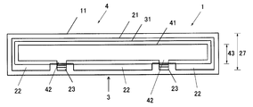
- FIG. 3 it is the conceptual diagram which extracted and showed the transparent conductive anode layer 21 and the electric power feeding pad part 23 for cathodes.
- FIG. 3 it is the conceptual diagram which extracted and showed the metal cathode layer 41.
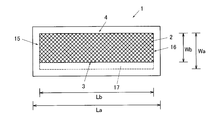
- FIG. 2 is a plan view of the long organic EL panel 1 showing a state where the long organic EL panel 1 shown in FIG. 1 emits light.
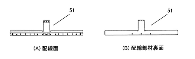
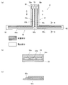
- A is a front view of the wiring member observed from the electrode exposure side
- (b) is an AA cross-sectional view thereof
- (c) is a BB cross-sectional view thereof.
- FIG. 2 is a cross-sectional perspective view of the long organic EL (illumination panel) 1 of FIG.
- FIG. 1 showing the AA cross section and the BB cross section in FIG.
- FIG. 1 shows the state which arranged the elongate organic EL (illumination panel) 1 of FIG. 1 in the longitudinal direction.
- FIG. 1 shows the state which arranged the elongate organic EL (illumination panel) 1 of FIG. 1 in the longitudinal direction.
- FIG. 1 shows the state which arranged the elongate organic EL (illumination panel) 1 of FIG. 1 in the longitudinal direction.
- the long organic EL panel 1 is an organic EL panel having a thin thickness and a rectangular planar shape. As shown in FIGS. 1 and 13, the long organic EL panel 1 is long and has a long length La with respect to the width Wa.
- the light emitting region 2 of the long organic EL panel 1 is as shown in FIG. 13 and is planar and rectangular.
- the light emitting region 2 has a long overall length Lb with respect to the width Wb.
- the width Wb of the light emitting region 2 is equal to or less than one third of the total length Lb of the light emitting region 2.
- the width Wb of the light emitting region 2 is narrow and is 5 cm or less. More preferably, the width Wb of the light emitting region 2 is 3 cm or less. More preferably, the width Wb of the light emitting region 2 is 2 cm or less.
- the total length Lb of the light emitting region 2 is 5 cm or more, and more desirably 10 cm or more.
- the light emitting region 2 of the long organic EL panel 1 is rectangular as described above, and is surrounded by parallel long sides 3 and 4 and short sides 15 and 16.
- the power feeding unit 17 for the light emitting region 2 is concentrated on one long side 3 side of the light emitting region 2 as shown in FIG.
- the long organic EL panel 1 is a bottom emission type organic EL panel in which an organic EL element 10 is laminated on a glass substrate 11 as shown in FIGS.
- the organic EL element 10 is sealed with the sealing layer 6.
- a printed board 71 is further attached to the sealing layer 6.
- the printed board 71 and the organic EL element 10 are wired by the wiring member 51.
- the wiring member 51 is a flexible printed wiring.
- the long organic EL panel 1 is obtained by laminating the organic EL element 10 on the glass substrate 11.
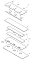
- the organic EL element 10 has a transparent conductive anode layer 21 as a transparent electrode layer and a metal cathode layer 41 as a metal layer, and a functional layer (light emitting functional layer) 31 between them. Is intervening.
- the transparent conductive anode layer 21 has a substantially rectangular shape in plan view as shown in FIGS. 11 and 12, and has an unevenness on one long side. Specifically, the transparent conductive anode layer 21 has two notches 25a and 25b on one long side as shown in FIGS. In other words, there are three protruding portions 26a, 26b, and 26c on one long side of the transparent conductive anode layer 21.
- the transparent conductive anode layer 21 is functionally distinguished into an anode layer main body region 27 that functions as an electrode and other pad regions 28.
- the anode layer main body region 27 is a rectangular region excluding the notches 25a and 25b and the protruding portions 26a, 26b, and 26c.
- the pad region 28 is a region where the protruding portions 26a, 26b, and 26c are formed.
- the protrusions 26a, 26b, and 26c described above are transparent electrode side power supply pad portions, and function as anode power supply pad portions 22a, 22b, and 22c in the present embodiment.
- the protrusions 26a, 26b, and 26c are transparent electrode-side power supply pad portions when attention is paid to the connection with the transparent conductive anode layer 21, and the electrode functions as anode power supply pad portions when attention is paid to the polarity of the electrodes.
- the names of the anode power supply pad portions 22a, 22b, and 22c are mainly used, but the anode power supply pad portions 22a, 22b, and 22c are also transparent electrode side power supply pad portions.
- the anode power supply pad portions 22 a, 22 b, and 22 c are a part of the transparent conductive anode layer 21 and an extended portion of the transparent conductive anode layer 21, and are terminals for energizing the functional layer (light emitting functional layer) 31.
- the shape of the protrusions 26a, 26b, and 26c is a rectangle. That is, the protrusions 26 a, 26 b and 26 c are long and thin rectangles along the long side 3 of the light emitting region 2.
- the three protrusions 26a, 26b, and 26c are arranged in this order from the left side of the drawing, and a notch 25a is provided between the protrusions 26a and 26b, and a notch 25b is provided between the protrusions 26b and 26c. is there.
- the ends in the longitudinal direction of the protrusions 26 a and 26 c at both ends are aligned with the ends of the anode layer main body region 27.
- the lengths L26a, L26b, and L26c in the longitudinal direction of the long organic EL panel 1 of the three protruding portions 26a, 26b, and 26c are all longer than the lengths L25a and L25b of the cutout portions 25a and 25b.
- the sum of the lengths L26a, L26b, and L26c of the protrusions 26a, 26b, and 26c is 60% or more of the length of the anode layer main body region 27, and more desirably 70% or more. More preferably, it is 80 percent or more.
- the connection length between the protrusions 26a, 26b, and 26c and the anode layer main body region 27 is the length L26a, L26b of the protrusions 26a, 26b, and 26c, Equal to L26c. Therefore, the total connection length of the protrusions 26a, 26b, 26c and the anode layer main body region 27 is 60% or more of the length of the anode layer main body region 27, more desirably 70% or more, and further preferably. Is 80 percent or more.
- the length of the protruding portions 26a and 26c arranged at both ends are the same, but the central protruding portion 26b is longer than the other two. Specifically, the length of the central protruding portion (central anode power supply pad portion) 26b is about twice as long as the other two.
- cathode power supply pad portions 23a and 23b are formed at the positions of the cutout portions 25a and 25b.
- the cathode power supply pad portions 23 a and 23 b are formed at the same time when the transparent conductive anode layer 21 is formed, and have the same material and thickness as the transparent conductive anode layer 21.
- the cathode power supply pad portions 23a and 23b are names focusing on the polarity of the electrodes, but the metal electrode side power supply pad portions are focused on the point of connection to the metal cathode layer 41 which is a metal layer.
- the names of the cathode power supply pad portions 23a and 23b are mainly used, but the cathode power supply pad portions 23a and 23b are also metal electrode side power supply pad portions.
- the cathode power supply pad portions 23 a and 23 b are island portions independent of the transparent conductive anode layer 21. That is, the transparent conductive anode layer 21 is formed in an island shape, and the cathode power supply pad portions 23 a and 23 b and the transparent conductive anode layer 21 are electrically insulated.
- the functional layer (light emitting functional layer) 31 is laminated on the anode layer main body region 27 of the transparent conductive anode layer 21 as shown in FIG. More specifically, as shown in FIGS. 11 and 12, the functional layer 31 is formed in a range that fits completely in the anode layer body region 27 of the transparent conductive anode layer 21.
- the metal cathode layer 41 is further laminated on the functional layer (light emitting functional layer) 31.
- the metal cathode layer 41 is also substantially rectangular in plan view as shown in FIGS.
- the metal cathode layer 41 also has irregularities on one long side. However, the positional relationship of the unevenness of the metal cathode layer 41 is opposite to that of the transparent conductive anode layer 21, and extended portions 42 a and 42 b protruding to portions corresponding to the cutout portions 25 a and 25 b of the transparent conductive anode layer 21. There is.
- the metal cathode layer 41 is also functionally divided into a metal cathode layer main body region 43 that functions as an electrode and other pad regions 45.
- the pad region 45 is a region where the extending portions 42 a and 42 b are formed, and the other portion is the metal cathode layer main body region 43.
- the metal cathode layer main body region 43 of the metal cathode layer 41 overlaps with the functional layer 31 and does not protrude from the functional layer 31.
- the extending portions 42 a and 42 b of the pad region 45 protrude from the functional layer 31.
- the positions of the extending portions 42 a and 42 b correspond to the cutout portions 25 a and 25 b of the transparent conductive anode layer 21. Therefore, the extending portions 42 a and 42 b of the metal cathode layer 41 overlap with the cathode power supply pad portions 23 a and 23 b provided in the notches 25 a and 25 b of the transparent conductive anode layer 21.
- the protruding end portions of the extending portions 42a and 42b of the metal cathode layer 41 reach the end portions of the cathode power supply pad portions 23a and 23b, and the extending portions 42a and 42b of the metal cathode layer 41 are supplied with power for the cathode. It overlaps with part of the pad portions 23a and 23b.
- the cathode power supply pad portions 23a and 23b may be entirely covered with the extending portions 42a and 42b of the metal cathode layer 41.
- a wiring member 51 shown in FIG. 14 is a member called a flexible printed wiring, and is formed by laminating a resin base layer 52, a metal conductive layer 53, and a covering layer 55.
- the wiring member 51 most of the metal conductive layer 53 is covered with the coating layer 55, and a part of the metal conductive layer 53 is exposed to the outside as an electrode.
- the wiring member 51 has a “T” shape having a horizontally long portion 56 and a vertically long portion 57. The vertically long portion 57 extends in a direction orthogonal to the horizontally long portion 56, and is connected to the longitudinal center of the horizontally long portion 56.
- the metal conductive layer 53 is divided into three systems. That is, on the base material layer 52, the left system metal conductive layer 53a, the middle system metal conductive layer 53b, and the right system metal conductive layer 53c are laminated. In the present embodiment, the vicinity of the free end side of the vertically long portion 57 functions as the terminal portion 58, and the three metal conductive layers 53 are all exposed near the free end side of the vertically long portion 57. In the present embodiment, the three metal conductive layers 53 are exposed at the terminal portion 58 to constitute an A-side left terminal 72a, a B-side terminal 73, and an A-side right terminal 72b.
- the horizontally long portion 56 functions as a pad portion, and the three metal conductive layers 53 are exposed at any portion of the horizontally long portion 56. That is, the horizontally long portion 56 includes an A side left pad 60a, a B side pad 60b, and an A side right pad 60c.
- the A-side left terminal 72a is connected to the A-side left pad 60a.
- the B side terminal 73 is connected to the B side pad 60b.
- the A side right terminal 72b is connected to the A side right pad 60c.
- the A-side left pad 60a and the A-side right pad 60c are connected to anode power supply pad portions (transparent electrode side power supply pad portions) 22a, 22b, and 22c.
- the B-side pad 60b is connected to the cathode power supply pad portion (metal electrode side power supply pad portion) 23a, 23b.
- the middle middle metal conductive layer 53 b passes through the center of the vertically long portion 57 and reaches the horizontally long portion 56.
- the middle system metal conductive layer 53b is exposed at the center of the horizontally long portion 56, and constitutes the B-side pad 60b.
- the exposed part (B side pad 60b) of the middle system metal conductive layer 53b is dot-like.
- the left metal conductive layer 53a reaches the horizontally long portion 56 along the vertically long portion 57, and further extends to the left side of the drawing along the horizontally long portion 56. And it exposes in the area
- the exposed portion of the left system metal conductive layer 53a (A-side left pad 60a) is linear and extends long.
- the right system metal conductive layer 53c is symmetrical with the left system metal conductive layer 53a.
- the right system metal conductive layer 53c is also similar to the left system metal conductive layer 53a, is linear, and extends long.
- the horizontally long portion 56 of the wiring member 51 is in contact with the pad regions 28 and 45 of the transparent conductive anode layer 21 and the metal cathode layer 41.
- the protrusions 26a, 26b, and 26c are referred to as a first protrusion 26a, a second protrusion 26b, and a third protrusion 26c.
- the two wiring members 51 are distinguished from the first wiring member 51a and the second wiring member 51b.
- the horizontally long portion 56 of each wiring member 51 is distinguished from the left wing side and the right wing side.
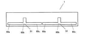
- the left wing side 61 of the first wiring member 51a is in the protruding portion 26a of the transparent conductive anode layer 21 (the anode power supply pad portion 22a and the transparent electrode side power supply pad portion).
- the exposed portion (A-side left pad 60a) of the system metal conductive layer 53a is in contact with the anode power supply pad portion 22a that is the extending portion of the transparent conductive anode layer 21.
- the A-side left pad 60a of the wiring member 51 overlaps the protruding portion 26a (anode feeding pad portion 22a) of the transparent conductive anode layer 21, as shown in the BB sectional view. .
- the central portion of the first wiring member 51a is in the cutout portion 25a of the transparent conductive anode layer 21, and the exposed portion (B side pad 60b) of the middle system metal conductive layer 53b is in contact with the cathode power supply pad portion 23a.
- the extended portion 42a of the metal cathode layer 41 is in contact with the island portion (cathode feed pad portion 23a) independent of the transparent conductive anode layer 21, Further, the B-side pad 60b of the wiring member 51 overlaps the island part (cathode power supply pad part 23a).
- the right wing side 62 of the first wiring member 51a is in the protruding portion 26b (anode feeding pad portion 22b) of the transparent conductive anode layer 21.
- the central protrusion 26b of the transparent conductive anode layer 21 is longer than the protrusions 26a and 26c at both ends. Therefore, the right wing side 62 of the first wiring member 51 a covers about half of the central protrusion 26 b of the transparent conductive anode layer 21.
- the exposed portion (A-side right pad 60c) of the right metal conductive layer 53c is in contact with about half of the anode power supply pad portion 22b extending from the transparent conductive anode layer 21.
- the left wing side 63 of the second wiring member 51b covers about half of the central protrusion 26b of the transparent conductive anode layer 21.
- the exposed portion of the left metal conductive layer 53a (A side left pad 60a) is in contact with about half of the anode power supply pad portion (transparent electrode side power supply pad portion) 22b extending from the transparent conductive anode layer 21.
- the central portion of the second wiring member 51b is in the cutout portion 25b of the transparent conductive anode layer 21, and the exposed portion (B side pad 60b) of the middle metal conductive layer 53b is in contact with the cathode power supply pad portion 23b. .
- the right wing side 65 of the second wiring member 51b is in the protruding portion 26c (anode feeding pad portion 22c) of the transparent conductive anode layer 21, and the exposed portion (A side right pad 60c) of the right system metal conductive layer 53c.
- the anode is in contact with the anode power supply pad portion 22 c, which is the extending portion of the transparent conductive anode layer 21.
- a sealing layer 6 that covers the organic EL element 10 is provided, and a printed circuit board 71 is provided so as to overlap the sealing layer 6.
- the sealing layer 6 seals at least a region corresponding to the light emitting region 2.
- the power feeding unit 17 does not have the sealing layer 6.
- the printed circuit board 71 is provided with anode receiving terminals 103a and 103c and a cathode receiving terminal 103b.
- the anode receiving terminals 103 a and 103 c and the cathode receiving terminal 103 b are all on the main surface opposite to the glass substrate 11.
- the terminal portions 58 of the two wiring members 51 a and 51 b are connected to the printed board 71.
- the A side left terminal 72a of the terminal portion 58 is connected to the anode receiving terminal 103a
- the B side terminal 73 is connected to the cathode receiving terminal 103b
- the A side right terminal 72b is connected to the anode receiving terminal 103c. ing.
- the organic EL element 10 is energized through the printed board 71. That is, a voltage is applied between the anode layer body region 27 of the transparent conductive anode layer 21 and the metal cathode layer body region 43 of the metal cathode layer 41, and a current flows through the functional layer 31 of the organic EL element 10.
- a voltage is applied between the anode layer body region 27 of the transparent conductive anode layer 21 and the metal cathode layer body region 43 of the metal cathode layer 41, and a current flows through the functional layer 31 of the organic EL element 10.
- there is a long feeding portion (anode feeding pad portions 22a, 22b, 22c) on one side of the anode layer main body region 27.
- the width of the anode layer body region 27 is narrow. Therefore, the resistance value between the power feeding portion and each portion of the anode layer main body region 27 is substantially uniform.
- the transparent electrode constituting the anode layer main body region 27 has a high resistance value, power is supplied from a wide range and the width of the region is narrow. Therefore, the resistance value between the power feeding portion and each portion of the anode layer main body region 27 has little variation. On the other hand, since the resistance value of the metal cathode layer 41 is low in the first place, the resistance value of the metal cathode layer body region 43 is uniform.
- the current supplied from the printed circuit board 71 flows from the terminal portion 58 of the wiring members 51a and 51b through the left system metal conductive layer 53a and the right system metal conductive layer 53c, and passes through the A side pads 60a and 60c. Then, power is supplied to anode power supply pad portions (transparent electrode side power supply pad portions) 22a, 22b, and 22c. Further, the current flows from the anode power supply pad portions 22a, 22b, and 22c to the anode layer main body region 27, flows to the functional layer (light emitting functional layer) 31, and further flows to the metal cathode layer 41 on the back surface side. Flows to the printed circuit board 71 via the part (metal electrode side power supply pad part) 23a and the middle metal conductive layer 53b.
- the transparent conductive anode layer 21 that functions as the anode-side electrode of the organic EL element 10 has a high electric resistance. For this reason, when the energization path is long, a voltage drop occurs on the terminal side, and a surface variation occurs in the amount of current passing through the functional layer 31.
- the long organic EL panel 1 of the present embodiment has a long light emitting region, and supplies power to the transparent conductive anode layer 21 from the long side.
- the energization path to the anode layer main body region 27 that functions as an anode is a rectangular region and is wide.
- the light emitting region is elongated and narrow, the energization path of the transparent conductive anode layer 21 itself is short. Therefore, it is difficult to cause a voltage drop at the end side of the transparent conductive anode layer 21, and the surface variation in the amount of current passing through the functional layer 31 is small.
- the metal conductive layer 53 of the wiring members 51a and 51b is a metal having a low resistance such as copper, the resistance value is low even if the energization distance changes somewhat, and the voltage drop can be ignored.
- the exposed portion of the metal conductive layer 53 is long along the light emitting region of the long organic EL panel 1.
- the metal conductive layer 53 is a metal having a low resistance, and even if the energization distance slightly changes, the voltage drop can be ignored. Therefore, the anode power supply pad is spread over the entire laterally long portion 56 of each wiring member 51. The voltages applied to the parts 22a, 22b and 22c are equal.
- the anode power supply pad portions 22a, 22b, and 22c are extended portions protruding from the anode layer main body region 27, and the length of the cross section of the portion connected to the anode layer main body region 27 is long. There is no portion that becomes a resistance when current flows from 22a, 22b, 22c to the anode layer body region 27. Further, since the width of the anode layer body region 27 itself is narrow, the voltage drop in the anode layer body region 27 is small. That is, the anode layer main body region 27 flows from one long side 3 toward the other long side 4 side, but the distance between the long side 3 on the power supply side and the long side 4 on the consumption side is short. Therefore, the potential of the other long side 4 of the anode layer main body region 27 is not significantly different from the vicinity of the long side 3 on the supply side. Therefore, the surface potential of the anode layer main body region 27 is uniform.
- the metal conductive layer 53 facing the anode layer body region 27 is a metal, the resistance is low in the first place, and the potential of the metal cathode layer body region 43 is uniform. Therefore, the voltage distribution between each part of the anode layer main body region 27 and each part of the metal cathode layer main body region 43 is uniform, and a current flows uniformly to the functional layer 31. Therefore, current flows uniformly from the entire surface of the anode layer body region 27 to the entire surface of the metal cathode layer body region 43. As a result, the planar light emitting region emits light evenly.
- the power feeding unit 17 is only on one long side 3 side of the light emitting region 2 and is not on the short side. Therefore, when the long organic EL panels 1 are arranged in the longitudinal direction as shown in FIG. 16, the non-light emitting area between the adjacent long organic EL panels 1 is small.
- FIG. 17 shows a configuration in which power is supplied by three wiring members 51.
- the anode power supply pad portions 22 a, 22 b and 22 c and the cathode power supply pad portions 23 a and 23 b are linearly arranged along one long side of the light emitting region 2. At both ends of the array, there are anode power supply pad portions 22a and 22c. This configuration is excellent in the action of flowing a current uniformly to the anode layer main body region 27 and can be recommended.
- the present invention is not limited to this configuration, and the cathode power supply pad portion 23 may be provided on either one end side or both end sides.
- the long organic EL panel 1 described above is a bottom emission type, but may be a top emission type.
- the anode power supply pad portions 22a, 22b, and 22c are extended portions of the transparent conductive anode layer 21, and are portions where the transparent conductive anode layer 21 is directly exposed. Other layers may be laminated on the surface of the film. Further, it may be an anode power supply pad portion made of a material different from that of the transparent conductive anode layer 21 and electrically connected to the transparent conductive anode layer 21. The same applies to the cathode power supply pad portion 23, which may be made of a material different from that of the transparent conductive anode layer 21 and electrically connected to the metal cathode layer 41.
- FIG. 1 is a non-light emitting surface side external view of an embodiment of a long organic EL panel 1 of the present invention.
- 2 is a light-emitting surface side external view showing the external shape of the glass substrate 11 and the light-emitting region 2 of the long organic EL panel 1 shown in FIG.
- FIG. 2 also shows a pattern of the functional layer 31 that does not actually appear in the appearance.
- the long organic EL panel 1 has a light emitting region 2 and an outer shape that are long in length (horizontal direction in FIG. 2) with respect to the width (vertical direction in FIG. 2).
- the size of the width and the length is appropriately determined according to the usage of the final lighting device.
- glass for forming an organic EL element 10 to be described later is used.
- the size is in accordance with the substrate 11, and preferably the width is 30 mm or less and the length is 100 mm or more.
- the long organic EL panel 1 includes an organic EL element 10 corresponding to the light emitting area 2 and capable of causing the light emitting area 2 to emit light, and preferably a glass substrate 11 for forming the organic EL element 10 thereon. More preferably, a wiring member 51 and a printed board 71 described later are included.
- the organic EL element 10 is an element for allowing light to be emitted from the light emitting region 2, and as described above, the light emitting region 2 is a long region having a long length with respect to the width.
- the organic EL element 10 corresponding to the light emitting region 2 includes one long side 3 parallel to the longitudinal direction and the other long side 4 facing the one long side 3 with the light emitting region 2 interposed therebetween.
- Such an organic EL element 10 includes a transparent conductive anode layer (front surface side electrode) 21, a functional layer (light emitting functional layer) 31 and a metal cathode layer (back side electrode) 41 according to the present invention. According to the voltage applied to the conductive anode layer 21 and the metal cathode layer 41, current flows through the functional layer 31 sandwiched between these overlapping portions, and thus the above-described light is emitted. In the organic EL element 10, a region where the transparent conductive anode layer 21, the functional layer (light emitting functional layer) 31 and the metal cathode layer 41 overlap is a light emitting region, which is a long rectangle.
- One characteristic of the organic EL element 10 is that it includes a cathode power supply pad portion 23 in addition to these three layers.
- FIG. 3 is a conceptual perspective view showing the shape of each pattern of the transparent conductive anode layer 21, the functional layer 31, and the metal cathode layer 41 and the positional relationship between them in an embodiment of the present invention.
- the one long side 3 side is a line on the lower side of the drawing as indicated by an arrow, and FIG. 3 also shows a cathode power supply pad portion 23.
- FIG. 4 is a conceptual diagram showing the transparent conductive anode layer 21 and the cathode power supply pad portion 23 extracted from FIG.
- the transparent conductive anode layer 21 is preferably a layer containing a transparent conductive metal oxide formed on the glass substrate 11, and one long side 3 side of the transparent conductive anode layer 21.
- the extending portion at least two or more, preferably three or more anode power supply pad portions 22 are included.
- the cathode power supply pad portion 23 is insulated from the transparent conductive anode layer 21, and preferably has the same material and the same layer thickness as the transparent conductive anode layer 21.
- a transparent conductive island layer is a layer that is in contact with an extended portion 42 on the long side 3 side of a metal cathode layer 41 to be described later, and is sandwiched between two anode power supply pad portions 22, Preferably there are two or more. That is, in the embodiment of FIG. 4, there are three anode power supply pad portions 22 on one long side 3 side, and there are two cathode power supply pad portions 23 sandwiched between the anode power supply pad portions 22. Power is supplied to the transparent conductive anode layer 21 and the metal cathode layer 41 only through the pad portion. The number of these pads may be determined as appropriate depending on the length and length, and at least two or more anode power supplies.
- the transparent conductive anode layer 21 is fed only through the pad portion 22, and there is one or more cathode feed pad portions 23, and the cathode feed pad portion 23 sandwiched between the two anode feed pad portions 22. Only the metal cathode layer 41 needs to be fed.
- FIG. 5 is a conceptual diagram showing the metal cathode layer 41 extracted from FIG.
- the metal cathode layer 41 includes the extending portion 42 on the long side 3 side of the metal cathode layer 41 described above, corresponding to the cathode power supply pad portion 23.
- the transparent conductive anode layer 21 In such a long organic EL panel 1, power is supplied to the transparent conductive anode layer 21 only through the anode power supply pad portion 22, and power supply to the metal cathode layer 41 is supplied to the cathode power supply pad portion. It is one feature of the present invention that it is done only through 23.
- the power supply pad portions existing at both ends are anode power supply pad portions 22.
- the transparent conductive anode layer 21 is one of the components of the organic EL element 10.
- the transparent conductive anode layer 21 applies an electric current from the outside while applying a positive potential to the metal cathode layer 41 to at least the functional layer 31 corresponding to the light emitting region 2 according to the present invention for the above-mentioned light emission. Has the function of flowing.
- the transparent conductive anode layer 21 includes at least an anode layer body region 27 including a light emitting region corresponding anode region in contact with the entire surface of the functional layer 31 corresponding to the light emitting region 2 in plan view, and the anode layer body region 27 continuously.
- the anode power supply pad portion 22 is provided and is used to supply a potential from the outside. That is, the anode power supply pad portion 22 is a region in which a part of the transparent conductive anode layer 21 extends from the anode layer main body region 27 to the one long side 3 according to the present invention.
- the material of the transparent conductive anode layer 21 may be a metal thin film such as aluminum or chromium as long as it is transparent, but is preferably a transparent conductive metal oxide, more preferably on the glass substrate 11.
- the transparent conductive metal oxide is formed directly.
- Such a transparent conductive metal oxide layer has strong adhesion to glass, is a highly reliable film even if it is a thin film, and can be easily patterned by wet etching or laser processing.
- the cathode power supply pad portion 23 is one of the components of the organic EL element 10 and supplies a negative potential to the transparent conductive anode layer 21 described above to the metal cathode layer 41 described later. , And has a function of relaying a current flowing from there to the outside.
- the material of the cathode power supply pad portion 23 may be a metal or the like as long as it is a conductive material, but is preferably the same material as the transparent conductive anode layer 21.
- the transparent conductive anode layer 21 and the cathode power supply pad portion 23 can be formed at the same time, and can be patterned at the same time, so that the cost can be reduced.
- Such a cathode power supply pad portion 23 needs to be insulated from the transparent conductive anode layer 21 and is preferably an island layer. That is, the cathode power supply pad portion 23 is separated from the transparent conductive anode layer 21 described above, and corresponds to an island floating on the glass substrate 11 (corresponding to the sea) if the transparent conductive anode layer 21 is regarded as land.
- the transparent conductive metal oxide layer (transparent conductive anode layer 21)
- a material of the transparent conductive metal oxide layer at least one selected from the group consisting of indium tin oxide (ITO), indium zinc oxide (IZO), tin oxide (SnO 2 ), and zinc oxide (ZnO) is included. preferable. In terms of effectively extracting light generated from the functional layer 31, ITO or IZO having high translucency is preferable, and ITO is more preferable.
- the transparent conductive metal oxide layer (transparent conductive anode layer 21) is preferably formed by sputtering or CVD.
- a resist is patterned by photolithography to remove unnecessary transparent conductive metal oxide film portions.
- the transparent conductive anode layer 21 (including the anode power supply pad portion 22) and the cathode power supply pad portion 23 are preferably sealed (the sealing pattern is not shown), thereby achieving the present invention.
- Such a long organic EL panel 1 is obtained.
- sealing is performed thereon.
- the functional layer 31 is one of the constituent elements of the organic EL element 10 and is formed by laminating a plurality of thin films including a light emitting layer containing an organic compound.
- the functional layer 31 can be formed of a known material such as a low molecular dye material or a conjugated polymer material used in a general organic EL element, and is formed by coating a polymer or oligomer of an organic compound. Although a thing can also be used, Preferably, it can be set as a high performance organic EL element by forming each layer into a film by the vacuum evaporation method.
- the functional layer 31 generally has a laminated multilayer structure including a plurality of layers including a hole injection layer, a hole transport layer, a light emitting layer, an electron transport layer, an electron injection layer, and the like. Further, each layer constituting these functional layers 31 is formed by vacuum deposition, sputtering, CVD, dipping, roll coating (printing), spin coating, bar coating, spraying, die coating, and flow coating. It is also possible to form by combining known methods such as methods.
- the functional layer 31 is required to be formed in a region including at least the entire region of the light emitting region 2 as viewed in a plan view as shown in FIG. As shown in FIG. 3, the functional layer 31 is preferably formed on the inner side of the anode layer main body region 27 on both the short sides and the other long sides from the viewpoint of ensuring sealing performance and long-term reliability. In the one long side 3 according to the present invention, the functional layer 31 is preferably formed on the inner side in the anode power supply pad portion 22. In a portion corresponding to the cathode power supply pad portion 23 other than the anode power supply pad portion 22, the functional layer 31 may be formed on the outer side, more preferably partly in direct contact with the glass substrate 11. preferable. The functional layer 31 is preferably formed in a complete rectangle that does not include irregularities on each side.
- the metal cathode layer 41 is one of the components of the organic EL element 10, and has a negative potential with respect to the transparent conductive anode layer 21 at least in the functional layer 31 corresponding to the light emitting region 2 for the above-described light emission. While applying, it has a function of flowing current from there to the outside.
- the metal cathode layer 41 includes a metal cathode layer main body region 43 and a cathode layer one long side extending portion 42. That is, as shown in FIGS.
- the metal cathode layer 41 includes at least a cathode layer body region 43 including a light emitting region corresponding cathode region in contact with the entire surface of the functional layer 31 corresponding to the light emitting region 2 in plan view. There is.
- the cathode layer main body region 43 has an extended portion on one long side 3 side, which is provided continuously and supplies the external potential and the like.
- the cathode layer functions as one long side extending portion 42.
- the cathode layer one long side extending portion 42 is a region in which a part of the metal cathode layer 41 extends from the cathode layer main body region 43 to the one long side 3 according to the present invention,
- the cathode layer one long side extending portion 42 is in direct contact with a part of the cathode power supply pad portion 23 and exhibits the above-described function.
- the cathode power supply pad portion 23 has a relay function. That is, by forming a part of the metal cathode layer 41 so as to overlap the cathode power supply pad portion 23, the metal cathode layer 41 exhibits the above-described function.
- the material of the metal cathode layer 41 according to the present invention is preferably aluminum or silver having a large reflectance and effective in improving the luminance.
- a vacuum deposition method is preferable, in which a high-purity film can be formed and the original physical properties of the material can be easily obtained.
- the metal cathode layer 41 has a cathode layer body region 43 corresponding to the light emitting region 2 as shown in plan view and FIG. 3 and FIG. Further, the cathode layer one long side extending portion 42 enhances the adhesion of the thin film to the glass substrate 11 in the portion until the cathode power supply pad portion 23 on the one long side 3 side is overlaid. From the viewpoint of improving long-term reliability, it is preferable that the glass substrate 11 is partly in direct contact with the glass substrate 11.
- the organic EL element 10 according to the present invention is preferably sealed in order to prevent moisture from entering from the outside.
- a flat glass plate is sealed with a sealing glass cap in which a depression is formed in a concave shape or a cap made of metal to cover the organic EL element, or a protective film is formed on the organic EL element and sealed.
- the cap sealing may be performed by adhering the cap and the substrate with an adhesive, or may be frit sealing that is fused with a glass frit in the case of a glass can sealing using a sealing glass cap.
- the sealing film for film sealing may be an inorganic film or an organic film, and its manufacturing method includes vapor deposition and sputtering, but it is preferable to form a silicon nitride film by CVD.
- a protective film made of PET or the like may be attached with an adhesive material in order to prevent scratches due to mechanical external force. In this way, the organic EL tile is completed.
- FIG. 6 is an external view showing an embodiment of the wiring member 51 according to the present invention
- FIG. 7 shows an embodiment of the long organic EL panel 1 of the present invention provided with the wiring member 51 of FIG. It is a non-light-emitting surface side external view.
- the wiring member 51 according to the present invention is a member for supplying power to the organic EL element 10 according to the present invention from the outside.
- the wiring member 51 includes a pad portion 60.
- the wiring member 51 is preferably a flat plate member having both the wiring surface and the wiring member back surface as both main surfaces as shown in FIG. More preferably, the back surface of the wiring member is an insulating surface.
- the anode pads (A side pads) 60a and 60c included in the pad portion 60 of the wiring member 51 are connected to the anode power supply pad portion 22, and the cathode pad (B side pad) 60b is used for the cathode. Connected to the power supply pad unit 23.
- the wiring member 51 may have a horizontally long portion 56 corresponding to the length of the power supply unit 17 in the power supply unit 17 of the long organic EL panel 1. That is, the long organic EL panel 1 has one long side 3 in which a pad portion including an anode power supply pad portion 22 and a cathode power supply pad portion 23 is arranged side by side. Then, one wiring member 51 having substantially the same length as the one long side 3 may be attached. However, even if the difference in coefficient of linear expansion between the wiring member 51 and the glass substrate 11 is large, two or more wiring members 51 are connected to each other so that the wiring member 51 and the glass substrate 11 are not warped or the wiring member 51 is not detached. It is desirable to attach to the long side 3.
- the structure of the two or more wiring members 51 is made the same from the viewpoint of reducing the cost and the process load by reducing the number of parts and enabling the mounting in the same mounting process.
- two adjacent wiring members 51 are connected in common only to one central anode power supply pad portion 22 b located between the wiring members 51.
- the wiring member 51 preferably includes a terminal portion as a conduction path between the pad portion 60 and an external power source.
- the terminal portion includes an anode terminal electrically connected to the anode pads (A-side pads) 60a and 60c, and a cathode terminal connected to the cathode pad (B-side pad) 60b.
- the terminal part is preferably a flat plate member having both the terminal surface and the terminal part back surface as main surfaces, and more preferably the terminal part back surface is an insulating surface.
- the wiring member 51 is a flat plate member having both the wiring surface and the wiring member back surface as both main surfaces, the terminal surface is included in the wiring surface, and the terminal partial back surface is the wiring member. More preferably, it is contained on the back surface.
- the terminal surface on which both terminals are arranged becomes a surface facing the organic EL element on the non-emitting main surface of the organic EL element, and can be a so-called single-sided wiring member. Since the current-carrying portion is not exposed to the panel, it is possible to obtain a panel having excellent safety with no risk of electric shock. Furthermore, the both terminals are preferably present in the light emission region in plan view, and the size of the organic EL panel 1 of the present invention can be made smaller than the size of the light emission region 2.
- the wiring member 51 As the wiring member 51 according to the present invention, a lead wire, copper foil, or aluminum foil can be used, but it is preferable to use a printed board.
- the wiring member 51 is more preferably a flexible printed circuit board (FPC). FPC is obtained by patterning wiring with copper foil or aluminum foil on polyimide or other organic film, and since it is thin, the thickness of the panel provided with it can be reduced and can be bent freely. .
- a conductive adhesive can be used to connect the pad portion 60 of the wiring member 51 to the power supply pad portions 22 and 23 of the organic EL element 10, but the connection reliability is improved by increasing the adhesive strength. From the viewpoint, it is desirable to perform thermocompression bonding using an anisotropic conductive film (ACF).
- ACF anisotropic conductive film
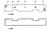
- FIG. 8 is a conceptual diagram showing an embodiment of the long organic EL panel 1 provided with a printed circuit board (PCB) 71.
- PCB printed circuit board
- the shielded part of the wiring member 51 that does not appear in appearance by being partially hidden by the printed circuit board 71 is represented by a dotted line.
- 8B is a cross-sectional view taken along the dashed-dotted line aa ′ in FIG. 8A.
- the printed circuit board 71 has a function of supplying power to the wiring member 51 from the outside.
- the printed board 71 is preferably sandwiched between the terminal portion of the wiring member 51 and the organic EL element 10.
- the printed circuit board 71 is on the side opposite to the organic EL element 10.
- a printed circuit board 71 is provided on the surface opposite to the glass substrate 11.
- the printed circuit board 71 has a circuit surface on which anode receiving terminals 103 a and 103 c connected to the anode terminals 72 a and 72 b of the wiring member 51 and a cathode receiving terminal 103 b connected to the cathode terminal 73 are arranged.
- the printed circuit board 71 is aligned so that the anode terminals 72a and 72b and the cathode terminal 73 of the wiring member 51 are connected to the anode receiving terminals 103a and 103c and the receiving terminal 103b.
- the receiving terminal portion including the anode receiving terminals 103a and 103c and the cathode receiving terminal 103b of the printed circuit board 71 is shielded and protected by the wiring member 51 according to the present invention, so that electric shock can be prevented and safety is improved. It can be shown.
- the printed circuit board 71 preferably includes a power receiving terminal 101 that receives power from the outside.
- the power receiving terminal 101 is more preferably disposed on the circuit surface. More preferably, the power receiving terminal 101 is a connector. As a result, it becomes easy to remove the power supply line from the outside to the printed circuit board (PCB) 71.
- the circuit wiring for distributing power from the power receiving terminal 101 to the receiving terminal portion is also disposed on the circuit surface, and more preferably, the exposed surface of the circuit wiring is insulated. As a result, electric shock on the printed circuit board 71 can be prevented, and safety can be improved.
- circuit surface of the printed circuit board 71 is provided with a protection circuit, it is desirable that even a multifunctional organic EL lighting panel is a panel that is unlikely to fail.
- a light control circuit for dimming the organic EL element 10 is provided on the circuit surface of the printed circuit board 71, it is desirable that the multifunctional organic EL panel 1 be obtained.
- the long organic EL panel 1 of the present invention was produced by the following procedure.
- the produced long organic EL panel 1 has a glass outer shape 142 mm ⁇ 23 mm which is the same as the outer shape, and a light emitting region 2 of 137.5 mm ⁇ 15.1 mm.
- transparent conductive anode layer (transparent conductive layer) 21 and cathode power supply pad portion (metal electrode side power supply pad portion) 23 are formed on the glass substrate 11 and the ITO film is wet etched. Then, an organic EL element forming substrate as shown in FIG. 9 was prepared.
- the anode power supply pad portion (transparent electrode side power supply pad portion) 22 having a length of 27 mm, the insulating region having a length of 5 mm, and the length 6 .6 mm ⁇ 4.54 mm wide cathode power supply pad portion 23 (transparent conductive island, metal electrode side power supply pad portion), 5 mm long insulating region, 55.6 mm long anode power supply pad portion 22, 5 mm length
- the negative electrode power supply pad portion 23 having a length of 6.6 mm and a width of 4.54 mm, the insulating region having a length of 5 mm, and the positive electrode power supply pad portion 22 having a length of 27 mm were patterned.
- an electron injection layer, an electron transport layer, a light emitting layer, a hole transport layer, and a hole injection layer are sequentially deposited on the organic EL element formation substrate as a functional layer 31 using a predetermined mask.
- a metal cathode layer 41 made of aluminum was laminated thereon by a vacuum vapor deposition method using a predetermined mask to form the organic EL element 10.
- a silicon nitride film is formed on the organic EL element 10 by a CVD method using a predetermined mask, and then a polysilazane is applied by a spray method and baked to form a sealing layer. did.
- a wiring member substrate flexible substrate
- ACF anisotropic conductive film
- the printed circuit board 71 having a thickness of 0.4 mm and a wiring layer on both sides was prepared.
- the printed circuit board 71 includes a connector component 101 on the circuit surface side of the printed circuit board 71 as a power receiving terminal that receives power from the outside.
- the printed circuit board 71 is provided with a Zener diode component 102 that is mounted and wired that operates as a protection circuit when a voltage of 12 V or more is applied between both electrode layers of the organic EL element 10.
- the printed circuit board 71 is obtained by insulating the surface of the circuit wiring other than the receiving terminals 103 to which the wiring member (flexible board) 51 is connected with a resist.
- the printed board 71 and the organic EL tile to which the wiring member (flexible board) 51 was bonded were assembled to produce the long organic EL panel 1 of the present invention shown in FIG. That is, the printed circuit board 71 is sandwiched between the terminal portion of the wiring member (flexible substrate) 51 and the organic EL tile, and the circuit board is connected to the wiring member (FPC) 51 side with a 50 ⁇ m thick double-sided tape. In this way, it was attached to the non-light emitting surface side of the organic EL tile, and then the terminal portion of the wiring member (FPC) 51 was connected to the receiving terminal 103 portion of the printed circuit board 71 by soldering.
Landscapes
- Engineering & Computer Science (AREA)
- General Engineering & Computer Science (AREA)
- Microelectronics & Electronic Packaging (AREA)
- Physics & Mathematics (AREA)
- Optics & Photonics (AREA)
- Electroluminescent Light Sources (AREA)
- Non-Portable Lighting Devices Or Systems Thereof (AREA)
- Planar Illumination Modules (AREA)
- Fastening Of Light Sources Or Lamp Holders (AREA)
Abstract
パネルを長手方向に並べたときに、面内輝度分布を小さく抑えながら、隣接するパネル間の非発光領域を狭くでき、かつ、パネル面積に対する発光領域面積の比率を大きくする。 長尺の発光領域および外形を有する長尺有機ELパネルにおいて、該発光領域に対応する有機EL素子が一長辺3を含み、該有機EL素子の透明導電性陽極層21への給電が、該透明導電性陽極層21の該一長辺側の該透明導電性陽極層21の延在部の少なくとも2以上の陽極用給電パッド部22を介してのみなされ、かつ、該有機EL素子の金属陰極層41への給電が、該金属陰極層41の該一長辺側の該陰極層の延在部が接する1以上の陰極用給電パッド部23であって、2つの陽極用給電パッド部22に挟まれた陰極用給電パッド部23を介してのみなされる、長尺有機ELパネル1。
Description
本発明は、有機EL(エレクトロルミネセンス)パネルに関わり、特に、幅に対して長さが長い長尺の有機ELパネルの給電構造に関するものである。
近年、白熱灯や蛍光灯に代わる照明装置として有機EL発光パネル(以下、有機ELパネルと称する)が注目され、多くの研究がなされている。ここで、有機ELパネルは、薄く且つ面状に発光する有機ELタイルに、外部から給電を行うための配線が施されたものである。有機ELタイルやパネル等の用語は国際規格IEC62868に定義されている。
有機ELタイルは、基材と有機EL素子によって構成されている。
有機ELタイルは、基材となるガラス基板や透明樹脂フィルム/金属シート等の基板上に、有機EL素子を形成したものである。有機EL素子は、一方又は双方が透光性を有し対向する電極対とその電極対の間に積層した機能層(発光機能層)とからなる。
一般に有機ELタイルは、さらに外部からの水分や酸素の侵入を防ぐように封止がなされる。
有機EL素子の電極間に電力を与えると、有機EL素子の中で電気的に励起された電子と正孔とが再結合し、有機ELタイルは発光する。有機ELタイルは、薄くて軽く面状に発光するという特徴を有する。
有機ELタイルは、基材となるガラス基板や透明樹脂フィルム/金属シート等の基板上に、有機EL素子を形成したものである。有機EL素子は、一方又は双方が透光性を有し対向する電極対とその電極対の間に積層した機能層(発光機能層)とからなる。
一般に有機ELタイルは、さらに外部からの水分や酸素の侵入を防ぐように封止がなされる。
有機EL素子の電極間に電力を与えると、有機EL素子の中で電気的に励起された電子と正孔とが再結合し、有機ELタイルは発光する。有機ELタイルは、薄くて軽く面状に発光するという特徴を有する。
有機ELパネルは、有機ELタイルに給電するための配線を施したものである。有機EL素子を構成する電極は、一般には薄膜であり、当該薄膜である電極に、リード線をハンダ付けすることや、フレキシブルプリント基板(FPC)などの素子用配線基板その他の配線部材を取り付けることにより給電配線が施される。
この様な面状に発光する特徴を有する有機ELタイルおよび有機ELパネルは、基材の形状や、薄膜電極と機能層の形状で決められる発光領域の形状を変えることにより、正方形や長方形、長尺、円形、三角形など、自由な外形、かつ、自由な発光領域形状にて面状に発光させることができる。そのため有機ELタイルおよび有機ELパネルは、様々な用途に対して優れた意匠性を有する照明装置を提供し得るものとして期待されている。
ところで、有機ELタイルの電極として一般に広く用いられている透光性の薄膜電極は抵抗が高い。そのために発光領域内に面内輝度分布を生じてしまう場合がある。特に、この面内輝度分布は発光領域が大きくなればなるほど大きくなる傾向があり、前記した用途多様性や前記した意匠性を損なったり、さらには、寿命や信頼性が不十分になったりする不具合を生じてしまうことが懸念される。
このような不具合の発生を防止するために、特許文献1は、輝度斑、輝度の経時変化が少なく信頼性の高く、且つ発光有効面積が大きいEL光源体が開示されている。
特許文献1に開示されたEL光源体は、EL発光素子および素子用配線基板により構成されている。特許文献1に開示されたEL光源体では、EL発光素子が、相互に対向して配置された素子基板と封止基板を有する。素子電極は、ITO(酸化インジウム錫)で構成される。
素子用配線基板には、ITO(酸化インジウム錫)で構成される素子電極に対向する面に、素子電極に沿って配置され素子電極に均等に接続される接続パターンが形成してある。そして素子電極と接続パターンが導電性接着剤で接続される。また素子用配線基板に外部と接続するためのパッド端子が形成してある。
特許文献1は、透光性の薄膜電極に沿うように素子用配線基板に接続パターンを形成・配置し、かつ、これらを接続することで、薄膜電極の抵抗による電圧降下に起因する発光層への印加電圧のばらつきを抑制するEL光源体を開示する。
特許文献1に開示されたEL光源体は、EL発光素子および素子用配線基板により構成されている。特許文献1に開示されたEL光源体では、EL発光素子が、相互に対向して配置された素子基板と封止基板を有する。素子電極は、ITO(酸化インジウム錫)で構成される。
素子用配線基板には、ITO(酸化インジウム錫)で構成される素子電極に対向する面に、素子電極に沿って配置され素子電極に均等に接続される接続パターンが形成してある。そして素子電極と接続パターンが導電性接着剤で接続される。また素子用配線基板に外部と接続するためのパッド端子が形成してある。
特許文献1は、透光性の薄膜電極に沿うように素子用配線基板に接続パターンを形成・配置し、かつ、これらを接続することで、薄膜電極の抵抗による電圧降下に起因する発光層への印加電圧のばらつきを抑制するEL光源体を開示する。
また特許文献2は、平面基板上に有機LED素子を形成した照明装置における技術的問題を解消し、かつ様々なサイズの照明装置に適用可能な有機LED照明装置要素を開示する。
特許文献2は、透明絶縁材料製の基板上に、ITOなどの透明電極、有機EL層および陰極電極をこの順に形成させてなるボトムエミッション型の有機LED素子が設けられた照明装置要素である。特許文献2に開示され前記基板は、断面形状のアスペクト比(幅/厚み)が1.5以上で、厚み400μm以下、幅は0.6mm~50mmの偏平長尺体からなり、有機LED素子が基板の主面上に形成され、かつ基板の長手方向に延びており、基板の主面の少なくとも一方の側面には、ITO透明電極への通電用電極が基板の長手方向に延びており、基板、有機LED素子および通電用電極は、透明保護膜によって被覆されており、基板の両端部には、前記有機LED素子への通電用端子が設けられていることを特徴とする照明装置要素を開示する。即ち特許文献2は、ガラス基板の側面に通電用電極を形成することで透光性薄膜電極層の抵抗を下げ、輝度分布を良くした偏平長尺体の有機EL照明装置を開示する。
特許文献2は、透明絶縁材料製の基板上に、ITOなどの透明電極、有機EL層および陰極電極をこの順に形成させてなるボトムエミッション型の有機LED素子が設けられた照明装置要素である。特許文献2に開示され前記基板は、断面形状のアスペクト比(幅/厚み)が1.5以上で、厚み400μm以下、幅は0.6mm~50mmの偏平長尺体からなり、有機LED素子が基板の主面上に形成され、かつ基板の長手方向に延びており、基板の主面の少なくとも一方の側面には、ITO透明電極への通電用電極が基板の長手方向に延びており、基板、有機LED素子および通電用電極は、透明保護膜によって被覆されており、基板の両端部には、前記有機LED素子への通電用端子が設けられていることを特徴とする照明装置要素を開示する。即ち特許文献2は、ガラス基板の側面に通電用電極を形成することで透光性薄膜電極層の抵抗を下げ、輝度分布を良くした偏平長尺体の有機EL照明装置を開示する。
特許文献1は、面内輝度分布を抑えるために、有機ELパネルの接続パターンにより、給電部分の薄膜電極の抵抗による電圧降下を低減する方法を開示する。しかしながら発光領域の薄膜電極の抵抗による電圧降下は、輝度分布により顕著な影響を与えるが、特許文献1は、その低減方法を開示するものではない。
また特許文献2の方法では、薄いガラス基板の側面に通電用電極を形成する必要があり、これは技術的に難しく歩留りや製造コストに大きな悪影響を与える。
本発明はこのような先行技術の問題点に鑑み為されたものであり、面内輝度分布を小さく抑えることができる有機ELパネルを提供することを課題とするものである。
また本発明は、長尺状の有機ELパネルを長手方向に並べたときに、隣接するパネル間の非発光領域を狭くでき、かつ、パネル面積に対する発光領域面積の比率を大きくできる長尺有機ELパネルを提供することを目的とする。
また本発明は、長尺状の有機ELパネルを長手方向に並べたときに、隣接するパネル間の非発光領域を狭くでき、かつ、パネル面積に対する発光領域面積の比率を大きくできる長尺有機ELパネルを提供することを目的とする。
本発明者らは上記課題に鑑み鋭意検討した結果、幅に対して長さが長い長尺の有機ELパネルの給電パッドを一方の長辺側のみに陽極/陰極/陽極/陰極/陽極の順に配置することが、上述した目的を達成するために有効であることを見出し、本発明を完成するに至った。
上記した課題を解決するための態様は、有機EL素子を有し、幅に対して長さが長い長尺の面状発光領域および外形を有する長尺の有機ELパネルにおいて、前記有機EL素子は、透明導電層と金属層の間に発光機能層を有し、前記発光領域に対応する前記有機EL素子が一長辺を含み、該有機EL素子の透明導電層への給電が、少なくとも2個以上の透明導電層の該一長辺側の延在部である透明電極側給電パッド部を介してのみなされ、かつ、該有機EL素子の金属層への給電が、該金属層の該一長辺側の延在部が接する1個以上の金属電極側給電パッド部であって、2つの該透明電極側給電パッド部に挟まれた金属電極側給電パッド部を介してのみなされることを特徴とする有機ELパネルである。
より推奨される態様は、幅に対して長さが長い長尺の、発光領域および外形を有する長尺有機ELパネルにおいて、該発光領域に対応する有機EL素子が一長辺を含み、該有機EL素子の透明導電性陽極層への給電が、少なくとも2個以上の、該陽極層の該一長辺側の延在部である、透明導電層用パッド部を介してのみなされ、かつ、該有機EL素子の金属陰極層への給電が、該陰極層の該一長辺側の延在部が接する1個以上の陰極用給電パッド部であって、2つの該陽極用給電パッド部に挟まれた陰極用給電パッド部を介してのみなされる、長尺有機ELパネルである。
このような長尺有機ELパネルは、パネルの発光領域面内を均一に発光させることができ、またパネルを長手方向に並置したときに隣接パネル間の非発光領域を狭小化でき、パネルの全面に対する発光領域の比率を最大化できる。
透明電極側給電パッド部の有機EL素子の長手方向に沿った総長さは、金属電極側給電パッド部の有機EL素子の長手方向に沿った総長さよりも長く、透明電極側給電パッド部と有機EL素子の面状発光領域との接続部分の有機EL素子の長手方向に沿った総長さは、金属電極側給電パッド部と有機EL素子の面状発光領域との接続部分の有機EL素子の長手方向に沿った総長さよりも長いことが望ましい。
同様の課題を解決するもう一つの態様は、有機EL素子と、有機EL素子に給電する配線を有し、有機EL素子は金属層と、透光性を有する薄膜状の透明電極層とを有し、前記透明電極層と金属層の間に発光機能層を有し、前記透明電極層と金属層の間に通電することによって所定の面状発光領域が発光する有機ELパネルであって、有機ELパネルの外形形状は幅に対して長さが長く、面状発光領域も幅に対して長さが長い有機ELパネルにおいて、面状発光領域の一方の長辺側に透明電極層の一部または透明電極層に繋がる透明電極側給電パッド部があり、面状発光領域の同じ長辺側に金属層の一部または金属層に繋がる金属電極側給電パッド部があり、透明電極側給電パッド部の有機EL素子の長手方向に沿った総長さは、金属電極側給電パッド部の有機EL素子の長手方向に沿った総長さよりも長く、透明電極側給電パッド部と有機EL素子の面状発光領域との接続部分の有機EL素子の長手方向に沿った総長さは、金属電極側給電パッド部と有機EL素子の面状発光領域との接続部分の有機EL素子の長手方向に沿った総長さよりも長いことを特徴とする有機ELパネルである。
上記した各態様において、透明電極側給電パッド部と、金属電極側給電パッド部が面状発光領域の長辺に沿って交互に配されており、一方の給電パッド部の間に他方の給電パッド部があることが望ましい。
上記した各態様において、複数の給電パッド部が面状発光領域の一方の側に直線状に並び、その中で両端に存在する給電パッド部が透明電極側給電パッド部であり、透明電極側給電パッド部と金属電極側給電パッド部が面状発光領域の長辺に沿って交互に配されていることが望ましい。
上記した各態様において、基板を有し、有機EL素子は基板に透明電極層と、発光機能層と、金属層が積層されたものであり、透明電極側給電パッド部は透明電極層の一部であって発光領域に相当する領域から発光領域の側面側に張り出した部分であり、基板に透明電極層と同一の素材によって形成されたアイランド部があり、アイランド部の一部又は全部に裏面側電極が重ねられて前記金属電極側給電パッド部が形成されていることが望ましい。
上記した各態様において、ガラス基板を有し、前記透明導電層は電気的には陽極層として機能し、前記金属層は電気的には陰極層として機能し、当該透明導電層は、前記ガラス基板上に形成された透明導電性金属酸化物を含む層であって、前記透明電極側給電パッド部を3個以上含み、かつ、前記金属電極側給電パッド部を2個以上含み、前記金属電極側給電パッド部が、前記透明導電層と同一の材料、かつ、同一の層厚みの透明導電性アイランド層であって、前記透明導電層と絶縁された透明導電性アイランド層であり、さらに、前記一長辺側において、両端に存在する給電パッド部が前記透明電極側給電パッド部であることが好ましい。
本態様によると、より発光領域面内を均一に発光させることができる。また本態様では、陰極用給電パッド部が、ガラス基板との密着性に優れる透明導電性金属酸化物層である透明導電性アイランド層なので、高信頼性の給電パッドを備える高信頼性のパネルとなる。
本態様によると、より発光領域面内を均一に発光させることができる。また本態様では、陰極用給電パッド部が、ガラス基板との密着性に優れる透明導電性金属酸化物層である透明導電性アイランド層なので、高信頼性の給電パッドを備える高信頼性のパネルとなる。
また本発明者らは、このような本発明の有機ELパネルについて、さらに検討し、陽極/陰極/陽極と配置された同形のフレキシブルプリント基板(FPC)を2つ並べて給電パッド部に接続することが、このようなパネルへの給電に有効であることを見出し、以下のような発明も完成させた。
即ち、本態様は、前記有機EL素子に外部から給電するための配線部材を2個以上備える前記した有機ELパネルであって、隣接する該配線部材が、それらの配線部材の間に位置する1個の前記透明電極側給電パッド部たる中央陽極用給電パッド部のみに共通に接続されている有機ELパネルである。
このような本態様の長尺有機ELパネルは、長尺パネルの複数の陽極用給電パッド部に対応して、分割した複数の配線部材を接続するので、配線部材と基板との線膨張係数差に起因して発生する温度変化による配線部材の外れの故障が起こり難い有機ELパネルとなり、長期に亘って安定給電され得る、高い信頼性の有機ELパネルとなる。
また、前記2個以上の配線部材は、同一部材とすることが好ましく、同一部材を使用することにより、部材点数を減らすことができ、配線部材取り付け工程も簡便になり生産性が向上する。
前記配線部材が、前記透明導電層用パッド部に接続されるA側パッド、及び前記金属電極側給電パッド部に接続されるB側パッドを含むパッド部分と、該A側パッドに電気接続されたA側端子、及び該B側パッドに接続されたB側端子を含む端子部分とを含み、かつ、該端子部分の両端子が、前記有機EL素子の非発光主面側であって平面視前記発光領域内に配されていることが望ましい。
本態様によると、パネル裏面に、露出した通電部分が無いので、感電を防止できる。
本態様によると、パネル裏面に、露出した通電部分が無いので、感電を防止できる。
さらに、前記配線部材に外部から給電するためのプリント基板を備える有機ELパネルであって、プリント基板は回路面に陽極受け端子と陰極受け端子が配され、該プリント基板が、前記配線部材の前記端子部分と前記有機EL素子との間にあり、プリント基板の前記陽極受け端子と前記陰極受け端子は前記有機EL素子とは反対側に向き、陽極受け端子及び陰極受け端子が、前記配線部材のA側端子及びB側端子に各々接続されていることが望ましい。
具体的には、前記配線部材に外部から給電するためのプリント基板を備えるパネルとすることが好ましく、該プリント基板は、前記端子部分と前記有機EL素子との間に挟持されていることが好ましく、該プリント基板の、前記有機EL素子とは反対側の、回路面に配された陽極受け端子、及び陰極受け端子は、前記陽極端子、及び前記陰極端子の対応する端子に各々接続されたパネルとすることが好ましい。
これらの態様によると、配線部材によりプリント基板の接続部分が保護されるため感電を防止できるとともに信頼性が向上し、かつ、発光領域の裏面で配線部材とプリント基板を接続できるため、パネル全体がコンパクトな構成にできる。
具体的には、前記配線部材に外部から給電するためのプリント基板を備えるパネルとすることが好ましく、該プリント基板は、前記端子部分と前記有機EL素子との間に挟持されていることが好ましく、該プリント基板の、前記有機EL素子とは反対側の、回路面に配された陽極受け端子、及び陰極受け端子は、前記陽極端子、及び前記陰極端子の対応する端子に各々接続されたパネルとすることが好ましい。
これらの態様によると、配線部材によりプリント基板の接続部分が保護されるため感電を防止できるとともに信頼性が向上し、かつ、発光領域の裏面で配線部材とプリント基板を接続できるため、パネル全体がコンパクトな構成にできる。
前記プリント基板が、外部から電力を受電する受電端子を有し、且つ、該受電端子から前記陽極受け端子、及び前記陰極受け端子まで配電する回路配線を有し、かつ、該回路配線の露出面が絶縁処理されていることが好ましい。
本態様によると、プリント基板での感電を防止できる。
本態様によると、プリント基板での感電を防止できる。
さらに、前記プリント基板は、前記回路面に保護回路を備えていることが好ましい。
本態様によると、パネルの非発光面側に保護回路を搭載することによりコンパクトな構成で、パネル保護の付加価値を付与することができる。
本態様によると、パネルの非発光面側に保護回路を搭載することによりコンパクトな構成で、パネル保護の付加価値を付与することができる。
さらに、前記プリント基板は、前記回路面に、前記有機EL素子を調光する調光回路を備えていることが好ましい。
本態様によると、パネルの非発光面側に調光回路を搭載することによりコンパクトな構成で、パネル調光の付加価値を付与することができる。
本態様によると、パネルの非発光面側に調光回路を搭載することによりコンパクトな構成で、パネル調光の付加価値を付与することができる。
本発明の有機ELパネルによれば、発光領域面内を均一に発光させることができ、パネルを長手方向に並置したときに隣接パネル間の非発光領域を狭小化し、かつ、パネル面積に対する発光領域面積の比率を最大化した照明器具を、安価に提供できる。
各部の詳細な説明に先立って、本発明の実施形態の長尺有機ELパネル1の概要について説明する。
長尺有機ELパネル1は、厚さが薄く、平面形状が長方形の有機ELパネルである。長尺有機ELパネル1は、図1、図13の様に、幅Waに対して全長Laが長く、長尺状である。
長尺有機ELパネル1の発光領域2は、図13の通りであり、面状であり、且つ長方形である。発光領域2は、幅Wbに対して全長Lbが長く、長尺状である。
発光領域2の幅Wbは、発光領域2の全長Lbの3分の1以下である。より望ましくは5分の1以下であり、さら望ましくは8分の1以下である。
また発光領域2の幅Wbは狭く、5cm以下である。より望ましくは発光領域2の幅Wbは3cm以下である。より好ましくは、発光領域2の幅Wbは2cm以下である。
発光領域2の全長Lbは、5cm以上であり、より望ましくは10cm以上である。
長尺有機ELパネル1は、厚さが薄く、平面形状が長方形の有機ELパネルである。長尺有機ELパネル1は、図1、図13の様に、幅Waに対して全長Laが長く、長尺状である。
長尺有機ELパネル1の発光領域2は、図13の通りであり、面状であり、且つ長方形である。発光領域2は、幅Wbに対して全長Lbが長く、長尺状である。
発光領域2の幅Wbは、発光領域2の全長Lbの3分の1以下である。より望ましくは5分の1以下であり、さら望ましくは8分の1以下である。
また発光領域2の幅Wbは狭く、5cm以下である。より望ましくは発光領域2の幅Wbは3cm以下である。より好ましくは、発光領域2の幅Wbは2cm以下である。
発光領域2の全長Lbは、5cm以上であり、より望ましくは10cm以上である。
長尺有機ELパネル1の発光領域2は前記した様に長方形であり、平行な長辺3,4と、短辺15,16に囲まれている。
本実施形態では、発光領域2に対する給電部17は、図13の様に発光領域2の一方の長辺3側に集中している。
本実施形態では、発光領域2に対する給電部17は、図13の様に発光領域2の一方の長辺3側に集中している。
長尺有機ELパネル1は、ボトムエミッション型の有機ELパネルであり、図11、図12の様にガラス基板11に、有機EL素子10が積層されたものである。また本実施形態では、有機EL素子10が封止層6で封止されている。
本実施形態の長尺有機ELパネル1では、さらに封止層6にプリント基板71が取り付けられている。そしてプリント基板71と有機EL素子10の間が配線部材51によって配線されている。本実施形態では、配線部材51は、フレキシブルプリント配線である。
本実施形態の長尺有機ELパネル1では、さらに封止層6にプリント基板71が取り付けられている。そしてプリント基板71と有機EL素子10の間が配線部材51によって配線されている。本実施形態では、配線部材51は、フレキシブルプリント配線である。
前記した様に長尺有機ELパネル1は、ガラス基板11に、有機EL素子10が積層されたものである。
有機EL素子10は、図11、図12の様に、透明電極層たる透明導電性陽極層21と、金属層たる金属陰極層41を有し、両者の間に機能層(発光機能層)31が介在するものである。
有機EL素子10は、図11、図12の様に、透明電極層たる透明導電性陽極層21と、金属層たる金属陰極層41を有し、両者の間に機能層(発光機能層)31が介在するものである。
本実施形態では、透明導電性陽極層21は、図11、図12の様に平面視が略長方形であり、その一方の長辺側に凹凸がある。具体的には、透明導電性陽極層21は、図11、図12の様にその一方の長辺側に2か所、切り欠き部25a,25bがある。逆にいえば、透明導電性陽極層21の一方の長辺側には3か所の突出部26a,26b,26cがある。
透明導電性陽極層21は、機能上、電極として機能する陽極層本体領域27と、それ以外のパッド領域28に区別される。
陽極層本体領域27は、切り欠き部25a,25b及び突出部26a,26b,26cを除く長方形の領域である。
パッド領域28は、突出部26a,26b,26cが形成された領域である。
透明導電性陽極層21は、機能上、電極として機能する陽極層本体領域27と、それ以外のパッド領域28に区別される。
陽極層本体領域27は、切り欠き部25a,25b及び突出部26a,26b,26cを除く長方形の領域である。
パッド領域28は、突出部26a,26b,26cが形成された領域である。
前記した突出部26a,26b,26cは、透明電極側給電パッド部であり、本実施形態では、陽極用給電パッド部22a,22b,22cとして機能する。
突出部26a,26b,26cは透明導電性陽極層21に繋がる点に注目すると透明電極側給電パッド部であり、電極の極性に注目すると陽極用給電パッド部として機能する。 実施形態においては、陽極用給電パッド部22a,22b,22cの名称を主として使用するが、陽極用給電パッド部22a,22b,22cは透明電極側給電パッド部でもある。
陽極用給電パッド部22a,22b,22cは透明導電性陽極層21の一部であって透明導電性陽極層21の延在部であり、機能層(発光機能層)31に通電するための端子として機能する。
突出部26a,26b,26cの形状は長方形である。即ち突出部26a,26b,26cは、発光領域2の長辺3に沿って長細い長方形である。
突出部26a,26b,26cは透明導電性陽極層21に繋がる点に注目すると透明電極側給電パッド部であり、電極の極性に注目すると陽極用給電パッド部として機能する。 実施形態においては、陽極用給電パッド部22a,22b,22cの名称を主として使用するが、陽極用給電パッド部22a,22b,22cは透明電極側給電パッド部でもある。
陽極用給電パッド部22a,22b,22cは透明導電性陽極層21の一部であって透明導電性陽極層21の延在部であり、機能層(発光機能層)31に通電するための端子として機能する。
突出部26a,26b,26cの形状は長方形である。即ち突出部26a,26b,26cは、発光領域2の長辺3に沿って長細い長方形である。
3箇所の突出部26a,26b,26cは、図面左側からこの順で並んでおり、突出部26a,26bの間に切り欠き部25aがあり、突出部26b,26cの間に切り欠き部25bがある。
両端の突出部26a,26cの長手方向の端部は、陽極層本体領域27の端部と揃っている。
3箇所の突出部26a,26b,26cの長尺有機ELパネル1の長手方向の長さL26a,L26b,L26cは、いずれも切り欠き部25a,25bの長さL25a,L25bに比べて長い。
突出部26a,26b,26cの長さL26a,L26b,L26cの合計は、陽極層本体領域27の長さの60パーセント以上であり、より望ましくは70パーセント以上である。またより好ましくは80パーセント以上である。
両端の突出部26a,26cの長手方向の端部は、陽極層本体領域27の端部と揃っている。
3箇所の突出部26a,26b,26cの長尺有機ELパネル1の長手方向の長さL26a,L26b,L26cは、いずれも切り欠き部25a,25bの長さL25a,L25bに比べて長い。
突出部26a,26b,26cの長さL26a,L26b,L26cの合計は、陽極層本体領域27の長さの60パーセント以上であり、より望ましくは70パーセント以上である。またより好ましくは80パーセント以上である。
突出部26a,26b,26cの形状は、長方形であるから、突出部26a,26b,26cと陽極層本体領域27との接続長さは、突出部26a,26b,26cの長さL26a,L26b,L26cと等しい。
従って、突出部26a,26b,26cと陽極層本体領域27との接続長さの合計は、陽極層本体領域27の長さの60パーセント以上であり、より望ましくは70パーセント以上であり、さらに好ましくは80パーセント以上である。
従って、突出部26a,26b,26cと陽極層本体領域27との接続長さの合計は、陽極層本体領域27の長さの60パーセント以上であり、より望ましくは70パーセント以上であり、さらに好ましくは80パーセント以上である。
本実施形態では、陽極層本体領域27の一方の長辺側に3箇所の突出部26a,26b,26cがあるが、その長さは一様ではない。本実施形態では、両端部に配された突出部26a,26cの長さは同じであるが、中央の突出部26bは他の二つよりも長い。具体的には、中央の突出部(中央陽極用給電パッド部)26bの長さは、他の二つの2倍程度の長さである。
本実施形態では、切り欠き部25a,25bの位置に陰極用給電パッド部23a,23bが形成されている。陰極用給電パッド部23a,23bは、透明導電性陽極層21を形成する際に同時に作られたものであり、透明導電性陽極層21と同一の材質及び厚さである。
陰極用給電パッド部23a,23bは、電極の極性に注目した名称であるが、金属層たる金属陰極層41に繋がる点に注目すると金属電極側給電パッド部である。本実施形態では、陰極用給電パッド部23a,23bの名称を主として使用するが、陰極用給電パッド部23a,23bは金属電極側給電パッド部でもある。
陰極用給電パッド部23a,23bは、透明導電性陽極層21から独立したアイランド部である。即ち透明導電性陽極層21は島状に形成されており、陰極用給電パッド部23a,23bと透明導電性陽極層21との間は電気的に絶縁されている。
陰極用給電パッド部23a,23bは、電極の極性に注目した名称であるが、金属層たる金属陰極層41に繋がる点に注目すると金属電極側給電パッド部である。本実施形態では、陰極用給電パッド部23a,23bの名称を主として使用するが、陰極用給電パッド部23a,23bは金属電極側給電パッド部でもある。
陰極用給電パッド部23a,23bは、透明導電性陽極層21から独立したアイランド部である。即ち透明導電性陽極層21は島状に形成されており、陰極用給電パッド部23a,23bと透明導電性陽極層21との間は電気的に絶縁されている。
機能層(発光機能層)31は、図11の様に透明導電性陽極層21の陽極層本体領域27に積層されている。より具体的には、図11、図12の様に、機能層31は、透明導電性陽極層21の陽極層本体領域27にすっぽりと納まる範囲に形成されている。
金属陰極層41は、さらに機能層(発光機能層)31に重ねて積層されている。金属陰極層41についても、図11、図12の様に平面視が略長方形である。金属陰極層41についてもその一方の長辺側に凹凸がある。ただし金属陰極層41の凹凸の位置関係は、透明導電性陽極層21とは逆であり、透明導電性陽極層21の切り欠き部25a,25bに相当する部分に突出した延在部42a,42bがある。
金属陰極層41についても、機能上、電極として機能する金属陰極層本体領域43と、それ以外のパッド領域45に区別される。
本実施形態では、パッド領域45は、延在部42a,42bが形成された領域であり、その他の部分は金属陰極層本体領域43である。
金属陰極層41の金属陰極層本体領域43は、機能層31と重なり、機能層31からはみ出さない。
本実施形態では、パッド領域45は、延在部42a,42bが形成された領域であり、その他の部分は金属陰極層本体領域43である。
金属陰極層41の金属陰極層本体領域43は、機能層31と重なり、機能層31からはみ出さない。
一方、パッド領域45の延在部42a,42bは、機能層31からはみ出す。延在部42a,42bの位置は、透明導電性陽極層21の切り欠き部25a,25bに対応する。そのため金属陰極層41の延在部42a,42bは、透明導電性陽極層21の切り欠き部25a,25bに設けられた陰極用給電パッド部23a,23bと重なる。
本実施形態では、金属陰極層41の延在部42a,42bの突端部分が、陰極用給電パッド部23a,23bの端部に届き、金属陰極層41の延在部42a,42bが陰極用給電パッド部23a,23bの一部と重なっている。
なお、陰極用給電パッド部23a,23bの全体を金属陰極層41の延在部42a,42bがすっぽりと覆う構造であってもよい。
本実施形態では、金属陰極層41の延在部42a,42bの突端部分が、陰極用給電パッド部23a,23bの端部に届き、金属陰極層41の延在部42a,42bが陰極用給電パッド部23a,23bの一部と重なっている。
なお、陰極用給電パッド部23a,23bの全体を金属陰極層41の延在部42a,42bがすっぽりと覆う構造であってもよい。
本実施形態では、有機EL素子10に配線部材51が2個接続され、二つの配線部材51を介して透明導電性陽極層21と金属陰極層41の間に通電される。
図14に示す配線部材51は、フレキシブルプリント配線と称される部材であり、樹脂製の基材層52と、金属導電層53及び被覆層55が積層されたものである。
配線部材51は、金属導電層53の大部分が被覆層55で覆われており、金属導電層53の一部が電極として外部に露出する。
本実施形態では、配線部材51は横長部56と、縦長部57を有する「T」字形状である。縦長部57は、横長部56と直交する方向に延び、横長部56の長手方向の中心に接繋がっている。
図14に示す配線部材51は、フレキシブルプリント配線と称される部材であり、樹脂製の基材層52と、金属導電層53及び被覆層55が積層されたものである。
配線部材51は、金属導電層53の大部分が被覆層55で覆われており、金属導電層53の一部が電極として外部に露出する。
本実施形態では、配線部材51は横長部56と、縦長部57を有する「T」字形状である。縦長部57は、横長部56と直交する方向に延び、横長部56の長手方向の中心に接繋がっている。
金属導電層53は、3系統に分かれている。即ち基材層52には、左系統金属導電層53aと、中系統金属導電層53bと、右系統金属導電層53cが積層されている。
本実施形態では、縦長部57の自由端側の先端近傍が端子部58として機能し、3系統の金属導電層53は、いずれも縦長部57の自由端側の先端近傍で露出している。
本実施形態では、端子部58に3系統の金属導電層53が露出し、A側左端子72a、B側端子73及びA側右端子72bを構成している。
また本実施形態では、横長部56がパッド部として機能し、3系統の金属導電層53は、横長部56のいずれかの部分で露出している。
即ち横長部56には、A側左パッド60a、B側パッド60b及びA側右パッド60cがある。
前記したA側左端子72aはA側左パッド60aに接続されている。B側端子73はB側パッド60bに接続されている。A側右端子72bはA側右パッド60cに接続されている。
なおA側左パッド60a及びA側右パッド60cは、陽極用給電パッド部(透明電極側給電パッド部)22a,22b,22cに接続される。またB側パッド60bは、陰極用給電パッド部(金属電極側給電パッド部)23a,23bに接続される。
本実施形態では、縦長部57の自由端側の先端近傍が端子部58として機能し、3系統の金属導電層53は、いずれも縦長部57の自由端側の先端近傍で露出している。
本実施形態では、端子部58に3系統の金属導電層53が露出し、A側左端子72a、B側端子73及びA側右端子72bを構成している。
また本実施形態では、横長部56がパッド部として機能し、3系統の金属導電層53は、横長部56のいずれかの部分で露出している。
即ち横長部56には、A側左パッド60a、B側パッド60b及びA側右パッド60cがある。
前記したA側左端子72aはA側左パッド60aに接続されている。B側端子73はB側パッド60bに接続されている。A側右端子72bはA側右パッド60cに接続されている。
なおA側左パッド60a及びA側右パッド60cは、陽極用給電パッド部(透明電極側給電パッド部)22a,22b,22cに接続される。またB側パッド60bは、陰極用給電パッド部(金属電極側給電パッド部)23a,23bに接続される。
以下、配線部材51の構造及び接続関係についてより詳しく説明する。
3系統の金属導電層53の内、中央の中系統金属導電層53bは、縦長部57の中心を通過して、横長部56に至っている。そして中系統金属導電層53bは横長部56の中心で露出し、B側パッド60bを構成している。中系統金属導電層53bの露出部分(B側パッド60b)は、点状である。
3系統の金属導電層53の内、中央の中系統金属導電層53bは、縦長部57の中心を通過して、横長部56に至っている。そして中系統金属導電層53bは横長部56の中心で露出し、B側パッド60bを構成している。中系統金属導電層53bの露出部分(B側パッド60b)は、点状である。
一方、左系統金属導電層53aは、縦長部57に沿って横長部56に至り、さらに横長部56に沿って図面左側に延びている。そして横長部56の幅の約半分の領域で露出し、A側左パッド60aを構成している。左系統金属導電層53aの露出部分(A側左パッド60a)は、線状であって長くのびている。
右系統金属導電層53cは、左系統金属導電層53aと対称形である。右系統金属導電層53cについても左系統金属導電層53aと同様であり、線状であって長くのびている。
右系統金属導電層53cは、左系統金属導電層53aと対称形である。右系統金属導電層53cについても左系統金属導電層53aと同様であり、線状であって長くのびている。
本実施形態では、透明導電性陽極層21及び金属陰極層41のパッド領域28,45に配線部材51の横長部56が当接されている。
説明の便宜上、突出部26a,26b,26cを第一突出部26a,第二突出部26b,第三突出部26cと称する。また二つの配線部材51を第一配線部材51a,第二配線部材51bと区別する。
さらに各配線部材51の横長部56を左翼側と右翼側に区別する。
説明の便宜上、突出部26a,26b,26cを第一突出部26a,第二突出部26b,第三突出部26cと称する。また二つの配線部材51を第一配線部材51a,第二配線部材51bと区別する。
さらに各配線部材51の横長部56を左翼側と右翼側に区別する。
本実施形態では、図11の様に、第一配線部材51aの左翼側61が、透明導電性陽極層21の突出部26a(陽極用給電パッド部22a 透明電極側給電パッド部)にあり、左系統金属導電層53aの露出部(A側左パッド60a)が透明導電性陽極層21の延在部たる陽極用給電パッド部22aと接している。
図15を参照しつつ説明すると、B-B断面図の様に、透明導電性陽極層21の突出部26a(陽極用給電パッド部22a)に配線部材51のA側左パッド60aが重なっている。
図15を参照しつつ説明すると、B-B断面図の様に、透明導電性陽極層21の突出部26a(陽極用給電パッド部22a)に配線部材51のA側左パッド60aが重なっている。
また第一配線部材51aの中心部分が透明導電性陽極層21の切り欠き部25aにあり、中系統金属導電層53bの露出部(B側パッド60b)が陰極用給電パッド部23aと接している。
図15を参照しつつ説明すると、A-A断面図の様に、透明導電性陽極層21から独立したアイランド部(陰極用給電パッド部23a)に金属陰極層41の延在部42aが接し、さらにアイランド部(陰極用給電パッド部23a)に配線部材51のB側パッド60bが重なっている。
図15を参照しつつ説明すると、A-A断面図の様に、透明導電性陽極層21から独立したアイランド部(陰極用給電パッド部23a)に金属陰極層41の延在部42aが接し、さらにアイランド部(陰極用給電パッド部23a)に配線部材51のB側パッド60bが重なっている。
また第一配線部材51aの右翼側62が、透明導電性陽極層21の突出部26b(陽極用給電パッド部22b)にある。
ここで透明導電性陽極層21の中央の突出部26bは、両端の突出部26a,cよりも長い。そのため、第一配線部材51aの右翼側62は、透明導電性陽極層21の中央の突出部26bの約半分を覆う。
そして右系統金属導電層53cの露出部(A側右パッド60c)が透明導電性陽極層21から延在部した陽極用給電パッド部22bの約半分と接している。
ここで透明導電性陽極層21の中央の突出部26bは、両端の突出部26a,cよりも長い。そのため、第一配線部材51aの右翼側62は、透明導電性陽極層21の中央の突出部26bの約半分を覆う。
そして右系統金属導電層53cの露出部(A側右パッド60c)が透明導電性陽極層21から延在部した陽極用給電パッド部22bの約半分と接している。
同様に、第二配線部材51bの左翼側63が、透明導電性陽極層21の中央の突出部26bの約半分を覆う。
そして左系統金属導電層53aの露出部(A側左パッド60a)が透明導電性陽極層21から延在部した陽極用給電パッド部(透明電極側給電パッド部)22bの約半分と接している。
また第二配線部材51bの中心部分が透明導電性陽極層21の切り欠き部25bにあり、中系統金属導電層53bの露出部(B側パッド60b)が陰極用給電パッド部23bと接している。
さらに第二配線部材51bの右翼側65が、透明導電性陽極層21の突出部26c(陽極用給電パッド部22c)にあり、右系統金属導電層53cの露出部(A側右パッド60c)が透明導電性陽極層21の延在部たる陽極用給電パッド部22cと接している。
そして左系統金属導電層53aの露出部(A側左パッド60a)が透明導電性陽極層21から延在部した陽極用給電パッド部(透明電極側給電パッド部)22bの約半分と接している。
また第二配線部材51bの中心部分が透明導電性陽極層21の切り欠き部25bにあり、中系統金属導電層53bの露出部(B側パッド60b)が陰極用給電パッド部23bと接している。
さらに第二配線部材51bの右翼側65が、透明導電性陽極層21の突出部26c(陽極用給電パッド部22c)にあり、右系統金属導電層53cの露出部(A側右パッド60c)が透明導電性陽極層21の延在部たる陽極用給電パッド部22cと接している。
本実施形態では、有機EL素子10を覆う封止層6が設けられており、さらに封止層6に重ねてプリント基板71が設けられている。なお封止層6は、少なくとも発光領域2に相当する領域を封止する。本実施形態では、給電部17には封止層6は無い。
プリント基板71には陽極受け端子103a,103c及び陰極受け端子103bが設けられている。陽極受け端子103a,103c及び陰極受け端子103bは、いずれもガラス基板11とは反対側の主面にある。
そして二つの配線部材51a,bの端子部58がプリント基板71に接続されている。より具体的には、端子部58のA側左端子72aが陽極受け端子103aに接続され、B側端子73が陰極受け端子103bに接続され、A側右端子72bが陽極受け端子103cに接続されている。
プリント基板71には陽極受け端子103a,103c及び陰極受け端子103bが設けられている。陽極受け端子103a,103c及び陰極受け端子103bは、いずれもガラス基板11とは反対側の主面にある。
そして二つの配線部材51a,bの端子部58がプリント基板71に接続されている。より具体的には、端子部58のA側左端子72aが陽極受け端子103aに接続され、B側端子73が陰極受け端子103bに接続され、A側右端子72bが陽極受け端子103cに接続されている。
そしてプリント基板71を介して有機EL素子10に通電される。即ち透明導電性陽極層21の陽極層本体領域27と、金属陰極層41の金属陰極層本体領域43との間に電圧が印加され、有機EL素子10の機能層31に電流が流される。
ここで本実施形態では、陽極層本体領域27の一辺側に長く給電部分(陽極用給電パッド部22a,22b,22c)がある。加えて陽極層本体領域27の幅が狭い。
そのため給電部分から陽極層本体領域27の各部間の抵抗値は略均一である。
即ち陽極層本体領域27を構成する透明電極は、抵抗値が高いものの、広い範囲から給電が行われ、且つ領域の幅が狭い。そのため給電部分から陽極層本体領域27の各部間の抵抗値はばらつきが少ない。
一方、金属陰極層41は、そもそも抵抗値が低いので、金属陰極層本体領域43の抵抗値は均一である。
ここで本実施形態では、陽極層本体領域27の一辺側に長く給電部分(陽極用給電パッド部22a,22b,22c)がある。加えて陽極層本体領域27の幅が狭い。
そのため給電部分から陽極層本体領域27の各部間の抵抗値は略均一である。
即ち陽極層本体領域27を構成する透明電極は、抵抗値が高いものの、広い範囲から給電が行われ、且つ領域の幅が狭い。そのため給電部分から陽極層本体領域27の各部間の抵抗値はばらつきが少ない。
一方、金属陰極層41は、そもそも抵抗値が低いので、金属陰極層本体領域43の抵抗値は均一である。
電流の流れに注目すると、プリント基板71から供給される電流は、配線部材51a,bの端子部58から左系統金属導電層53a及び右系統金属導電層53cを流れ、A側パッド60a,60cを経て陽極用給電パッド部(透明電極側給電パッド部)22a,22b,22cに通電される。そしてさらに電流は陽極用給電パッド部22a,22b,22cから陽極層本体領域27に流れて、機能層(発光機能層)31に流れ、さらに裏面側の金属陰極層41に流れ、陰極用給電パッド部(金属電極側給電パッド部)23a、中系統金属導電層53bを経由してプリント基板71に流れる。
ここで本実施形態では、有機EL素子10の陽極側の電極として機能するのは、透明導電性陽極層21であり、電気抵抗が高い。そのため通電経路が長いと、末端側で電圧降下をきたし、機能層31を通過する電流量に面的なばらつきが生じる。
これに対して本実施形態の長尺有機ELパネル1は、発光領域が長細く、透明導電性陽極層21に対して長辺側から給電している。しかも陽極として機能する陽極層本体領域27に至る通電路は、長方形の領域であり幅広い。さらに発光領域は細長く、幅が狭いから、透明導電性陽極層21自身の通電経路が短い。そのため透明導電性陽極層21の末端側で電圧降下をきたし難く、機能層31を通過する電流量に面的なばらつきは小さい。
これに対して本実施形態の長尺有機ELパネル1は、発光領域が長細く、透明導電性陽極層21に対して長辺側から給電している。しかも陽極として機能する陽極層本体領域27に至る通電路は、長方形の領域であり幅広い。さらに発光領域は細長く、幅が狭いから、透明導電性陽極層21自身の通電経路が短い。そのため透明導電性陽極層21の末端側で電圧降下をきたし難く、機能層31を通過する電流量に面的なばらつきは小さい。
具体的に説明すると、配線部材51a,bの金属導電層53は、銅等の抵抗の低い金属であるから、通電距離が多少変わっても抵抗値は低く、電圧降下は無視できる。
本実施形態では、透明導電性陽極層21に繋がる配線部材51a,bにおいて、金属導電層53の露出部分は、長尺有機ELパネル1の発光領域に沿って長い。しかしながら、前記した様に、金属導電層53は抵抗の低い金属であり、通電距離が多少変わっても電圧降下は無視できるから、各配線部材51の横長部56の全域に渡って陽極用給電パッド部22a,22b,22cに印加される電圧は等しい。
本実施形態では、透明導電性陽極層21に繋がる配線部材51a,bにおいて、金属導電層53の露出部分は、長尺有機ELパネル1の発光領域に沿って長い。しかしながら、前記した様に、金属導電層53は抵抗の低い金属であり、通電距離が多少変わっても電圧降下は無視できるから、各配線部材51の横長部56の全域に渡って陽極用給電パッド部22a,22b,22cに印加される電圧は等しい。
また陽極用給電パッド部22a,22b,22cは、陽極層本体領域27から突出した延在部であり、且つ陽極層本体領域27と繋がる部分の断面の長さが長いから、陽極用給電パッド部22a,22b,22cから陽極層本体領域27に電流が流れる際に抵抗となる部分は無い。
さらに陽極層本体領域27自体の幅が狭いから、陽極層本体領域27における電圧降下は少ない。
即ち陽極層本体領域27は、一方の長辺3から他方の長辺4側に向かって流れるが、給電側の長辺3と、消費側の長辺4との距離は短い。そのため陽極層本体領域27の他方の長辺4の電位は、供給側の長辺3近傍と大差ない。
そのため陽極層本体領域27の表面の電位は均一である。
さらに陽極層本体領域27自体の幅が狭いから、陽極層本体領域27における電圧降下は少ない。
即ち陽極層本体領域27は、一方の長辺3から他方の長辺4側に向かって流れるが、給電側の長辺3と、消費側の長辺4との距離は短い。そのため陽極層本体領域27の他方の長辺4の電位は、供給側の長辺3近傍と大差ない。
そのため陽極層本体領域27の表面の電位は均一である。
さらに陽極層本体領域27に対向する金属導電層53は、金属であるからそもそも抵抗が低く、金属陰極層本体領域43の電位は均一である。
そのため陽極層本体領域27各部と金属陰極層本体領域43の各部間の電圧分布は均等であり、機能層31に均一に電流が流れる。そのため陽極層本体領域27の全面から金属陰極層本体領域43の全面に電流が均等に流れる。
その結果、面状の発光領域は均等に発光する。
そのため陽極層本体領域27各部と金属陰極層本体領域43の各部間の電圧分布は均等であり、機能層31に均一に電流が流れる。そのため陽極層本体領域27の全面から金属陰極層本体領域43の全面に電流が均等に流れる。
その結果、面状の発光領域は均等に発光する。
また本実施形態の長尺有機ELパネル1は、給電部17が発光領域2の一方の長辺3側にのみあり、短辺側にはない。そのため図16の様に長尺有機ELパネル1を長手方向に並べたときに、隣接する長尺有機ELパネル1間の非発光領域が小さい。
上記した実施形態では、2本の配線部材51a,bによって機能層31に給電したが、1本又は3本以上の配線部材51によって給電を行ってもよい。図17は、3本の配線部材51によって給電を行う構成を示している。
前記した実施形態では、陽極用給電パッド部22a,22b,22cと、陰極用給電パッド部23a,23bが発光領域2の一長辺に沿って直線的に並んでいる。そして配列の両端側には、陽極用給電パッド部22a,22cがある。この構成は、陽極層本体領域27に対して均等に電流を流す作用に優れ、推奨できる。しかしながら本発明はこの構成に限定されるものではなく、いずれか一端側、又は両端側に陰極用給電パッド部23があってもよい。
上記した長尺有機ELパネル1は、ボトムエミッション型のものであるが、トップエミッション型であってもよい。
前記した実施形態では、陽極用給電パッド部22a,22b,22cと、陰極用給電パッド部23a,23bが発光領域2の一長辺に沿って直線的に並んでいる。そして配列の両端側には、陽極用給電パッド部22a,22cがある。この構成は、陽極層本体領域27に対して均等に電流を流す作用に優れ、推奨できる。しかしながら本発明はこの構成に限定されるものではなく、いずれか一端側、又は両端側に陰極用給電パッド部23があってもよい。
上記した長尺有機ELパネル1は、ボトムエミッション型のものであるが、トップエミッション型であってもよい。
本実施形態では、陽極用給電パッド部22a,22b,22cは、透明導電性陽極層21の延長部分であり、透明導電性陽極層21が直接露出した部位であるが、透明導電性陽極層21の表面に他の層が積層されたものであってもよい。
また透明導電性陽極層21とは別の素材で作られた陽極用給電パッド部であって、透明導電性陽極層21に電気的に接続されたものであってもよい。
陰極用給電パッド部23についても同様であり、透明導電性陽極層21とは別の素材で作られ、金属陰極層41に電気的に接続されたものであってもよい。
また透明導電性陽極層21とは別の素材で作られた陽極用給電パッド部であって、透明導電性陽極層21に電気的に接続されたものであってもよい。
陰極用給電パッド部23についても同様であり、透明導電性陽極層21とは別の素材で作られ、金属陰極層41に電気的に接続されたものであってもよい。
以上、長尺有機ELパネル1の概略の構成について説明したが、以下に各部の構成について、詳細な構造および製造方法を含めて、図を参照しながら説明する。
(長尺有機ELパネル1)
図1は本発明の長尺有機ELパネル1の一実施例の非発光面側外観図である。また、図2は、図1に示す長尺有機ELパネル1のガラス基板11の外形および発光領域2を示す発光面側外観図である。参考のため、図2には、実際には外観に表れない機能層31のパターンも図示されている。
図1は本発明の長尺有機ELパネル1の一実施例の非発光面側外観図である。また、図2は、図1に示す長尺有機ELパネル1のガラス基板11の外形および発光領域2を示す発光面側外観図である。参考のため、図2には、実際には外観に表れない機能層31のパターンも図示されている。
図2に示すように、長尺有機ELパネル1は、幅(図2の上下方向)に対して長さ(図2の左右方向)が長い長尺の、発光領域2および外形を有する。この幅や長さの大きさは、最終的な照明装置の使用態様に応じて、適宜決められるものであり、好ましい実施態様としては、後述する有機EL素子10をその上に形成するためのガラス基板11に準じた大きさとなり、好適には、幅は30mm以下で長さは100mm以上である。
長尺有機ELパネル1は、前記発光領域2に対応し、発光領域2を発光させることができる有機EL素子10を含み、好ましくはこの有機EL素子10をその上に形成するためのガラス基板11を含み、より好ましくは後述する配線部材51やプリント基板71を含む。
(有機EL素子10)
本発明に係る有機EL素子10は、発光領域2から光を放射可能とするための素子であり、前述したように発光領域2は、幅に対して長さが長い長尺の領域なので、この発光領域2に対応する有機EL素子10は、前記長尺方向に平行な、一長辺3、及びこの一長辺3と発光領域2を挟んで対向する他長辺4を含むこととなる。
本発明に係る有機EL素子10は、発光領域2から光を放射可能とするための素子であり、前述したように発光領域2は、幅に対して長さが長い長尺の領域なので、この発光領域2に対応する有機EL素子10は、前記長尺方向に平行な、一長辺3、及びこの一長辺3と発光領域2を挟んで対向する他長辺4を含むこととなる。
このような有機EL素子10は、本発明に係る透明導電性陽極層(表面側電極)21、機能層(発光機能層)31 、及び金属陰極層(裏面側電極)41を含み、この透明導電性陽極層21、及び金属陰極層41に印加される電圧に応じて、これらの重畳部分に挟持された機能層31に電流が流れることで、前述の光を放射することとなる。
有機EL素子10では、透明導電性陽極層21、機能層(発光機能層)31 、及び金属陰極層41が重なった領域が発光領域であり、長尺の長方形である。
有機EL素子10は、これら3つの層以外に、陰極用給電パッド部23を含むことを一つの特徴とする。
有機EL素子10では、透明導電性陽極層21、機能層(発光機能層)31 、及び金属陰極層41が重なった領域が発光領域であり、長尺の長方形である。
有機EL素子10は、これら3つの層以外に、陰極用給電パッド部23を含むことを一つの特徴とする。
図3は、本発明の一実施形態における、透明導電性陽極層21、機能層31、及び金属陰極層41の各々のパターンの形状、及び相互の位置関係を示す概念透視図である。図3において、前記一長辺3側は、矢印で示すように図面下側のラインであり、また、図3には、陰極用給電パッド部23も示されている。
図4は、図3において、透明導電性陽極層21、及び陰極用給電パッド部23を抜き出して示した概念図である。
図4に示すように、透明導電性陽極層21は、好ましくはガラス基板11上に形成された透明導電性金属酸化物を含む層であり、該透明導電性陽極層21の一長辺3側の延在部として、少なくとも2個以上、好ましくは3個以上の陽極用給電パッド部22を含む。また、図4に示すように、陰極用給電パッド部23は、前記透明導電性陽極層21と絶縁された、好ましくは、透明導電性陽極層21と同一の材料、かつ、同一の層厚みの透明導電性アイランド層であり、後述する金属陰極層41の一長辺3側の延在部42が接し、かつ、2つの陽極用給電パッド部22に挟まれた層であり、1個以上、好ましくは2個以上存在する。即ち、図4の実施形態では、一長辺3側に3つの陽極用給電パッド部22があり、その陽極用給電パッド部22に挟まれた2つの陰極用給電パッド部23があり、これらのパッド部を介してのみ透明導電性陽極層21および金属陰極層41に給電されるが、これらのパッドの数は長尺の大きさや長さによって適宜決められればよく、少なくとも2以上の陽極用給電パッド部22を介してのみ透明導電性陽極層21に給電され、1以上の陰極用給電パッド部23があって2つの陽極用給電パッド部22に挟まれた陰極用給電パッド部23を介してのみ金属陰極層41に給電されればよい。
図5は、図3において、金属陰極層41を抜き出して示した概念図である。
図5に示すように、金属陰極層41は、陰極用給電パッド部23に対応して、前述した金属陰極層41の一長辺3側の延在部42を含む。
このような長尺有機ELパネル1において、透明導電性陽極層21への給電が、陽極用給電パッド部22を介してのみなされ、かつ、金属陰極層41への給電が、陰極用給電パッド部23を介してのみなされることが本発明の一つの特徴である。また、好ましくは、一長辺3側において、両端に存在する給電パッド部が陽極用給電パッド部22である。
(透明導電性陽極層21、陰極用給電パッド部23)
本発明に係る透明導電性陽極層21は、有機EL素子10の構成要素の一つである。透明導電性陽極層21は、前述の光放射のため、少なくとも本発明に係る発光領域2に対応する機能層31 に、金属陰極層41に対しプラスの電位を印加しつつ、外部から、電流を流す機能を有する。
透明導電性陽極層21は、少なくとも、平面視前記発光領域2に対応する機能層31の全面に接する発光領域対応陽極領域を含む陽極層本体領域27と、この陽極層本体領域27に連続して設けられ、かつ、前記外部からの電位等を供給するための、前記陽極用給電パッド部22を含む。
即ち、陽極用給電パッド部22は、前記透明導電性陽極層21の一部が、前記陽極層本体領域27から本発明に係る一長辺3側に、延在した領域である。
本発明に係る透明導電性陽極層21は、有機EL素子10の構成要素の一つである。透明導電性陽極層21は、前述の光放射のため、少なくとも本発明に係る発光領域2に対応する機能層31 に、金属陰極層41に対しプラスの電位を印加しつつ、外部から、電流を流す機能を有する。
透明導電性陽極層21は、少なくとも、平面視前記発光領域2に対応する機能層31の全面に接する発光領域対応陽極領域を含む陽極層本体領域27と、この陽極層本体領域27に連続して設けられ、かつ、前記外部からの電位等を供給するための、前記陽極用給電パッド部22を含む。
即ち、陽極用給電パッド部22は、前記透明導電性陽極層21の一部が、前記陽極層本体領域27から本発明に係る一長辺3側に、延在した領域である。
透明導電性陽極層21の材料としては、透明であれば、アルミニウムやクロム等の金属薄膜であってもよいが、透明導電性金属酸化物であることが好ましく、より好ましくは、ガラス基板11に直接形成された透明導電性金属酸化物とすることである。このような透明導電性金属酸化物層は、ガラスとの密着力が強く、薄膜であっても信頼性の高い膜であり、かつ、ウェットエッチングやレーザー加工によるパターニングが容易である。
本発明に係る陰極用給電パッド部23は、有機EL素子10の構成要素の一つであり、後述する金属陰極層41に、前記した透明導電性陽極層21に対しマイナスの電位を供給しつつ、そこから外部に流れる電流を中継する機能を有する。
陰極用給電パッド部23の材料としては、導電性を有する材料であれば金属等であってもよいが、前記透明導電性陽極層21と同じ材料であることが好ましく、このようにすることで、透明導電性陽極層21、およびこの陰極用給電パッド部23とを、同時に形成可能であり、さらに、同時にパターニング可能であるため、コストを下げることができる。このような陰極用給電パッド部23は、前記透明導電性陽極層21と絶縁されていることを要し、好ましくは、アイランド層になっていることが望ましい。
即ち陰極用給電パッド部23は、前記した透明導電性陽極層21から切り離されており、透明導電性陽極層21を陸と見立てるならばガラス基板11(海に相当)に浮かぶ島に相当する。
即ち陰極用給電パッド部23は、前記した透明導電性陽極層21から切り離されており、透明導電性陽極層21を陸と見立てるならばガラス基板11(海に相当)に浮かぶ島に相当する。
前記透明導電性金属酸化物層(透明導電性陽極層21)の材料および製造方法について以下に述べる。
透明導電性金属酸化物層の材料としては、酸化インジウム錫(ITO)、インジウム亜鉛酸化物(IZO)、酸化錫(SnO2 )、及び酸化亜鉛(ZnO)からなる群から選ばれる1種以上が好ましい。
機能層31から発生した光を効果的に取り出せる点では、透光性が高いITOあるいはIZOが好ましく、より好ましくはITOである。透明導電性金属酸化物層(透明導電性陽極層21)は、スパッタ法、又はCVD法によって成膜されたものであることが好ましい。また、この透明導電性金属酸化物層をパターニングする方法としては、ガラス表面の全面に透明導電性金属酸化物層を形成後、フォトリソグラフィーによりレジストをパターニングし不要な透明導電性金属酸化膜部分をウェットエッチングにより化学的に取り除く方法や、レーザービームを照射して物理的に不要部分を取り除く方法がある。
透明導電性金属酸化物層の材料としては、酸化インジウム錫(ITO)、インジウム亜鉛酸化物(IZO)、酸化錫(SnO2 )、及び酸化亜鉛(ZnO)からなる群から選ばれる1種以上が好ましい。
機能層31から発生した光を効果的に取り出せる点では、透光性が高いITOあるいはIZOが好ましく、より好ましくはITOである。透明導電性金属酸化物層(透明導電性陽極層21)は、スパッタ法、又はCVD法によって成膜されたものであることが好ましい。また、この透明導電性金属酸化物層をパターニングする方法としては、ガラス表面の全面に透明導電性金属酸化物層を形成後、フォトリソグラフィーによりレジストをパターニングし不要な透明導電性金属酸化膜部分をウェットエッチングにより化学的に取り除く方法や、レーザービームを照射して物理的に不要部分を取り除く方法がある。
これら透明導電性陽極層21(陽極用給電パッド部22を含む。)及び陰極用給電パッド部23上に、好ましくは封止(封止のパターンは図示せず)を行うことで、本発明に係る長尺有機ELパネル1は得られることとなる。
好ましくはガラス基板11上に形成された透明導電性陽極層21、機能層31、さらに金属陰極層41を形成後、これらの上に封止を行う。
好ましくはガラス基板11上に形成された透明導電性陽極層21、機能層31、さらに金属陰極層41を形成後、これらの上に封止を行う。
(機能層31)
前記機能層31は、有機EL素子10の構成要素の一つであり、有機化合物を含有する発光層を含む複数の薄膜が積層されたものである。
機能層31は、一般的な有機EL素子に用いられている低分子系色素材料や、共役系高分子材料などの公知のもので形成することができ、有機化合物のポリマーやオリゴマーを塗布形成したものを用いることもできるが、好ましくは、各層をいずれも真空蒸着法によって成膜することにより、高性能の有機EL素子とすることができる。
機能層31は、正孔注入層、正孔輸送層、発光層、電子輸送層、電子注入層などを含む、複数の層からなる積層多層構造であることが一般的である。さらに、これらの機能層31を構成する各層は、真空蒸着法やスパッタ法、CVD法、ディッピング法、ロールコート法(印刷法)、スピンコート法、バーコート法、スプレー法、ダイコート法、フローコート法など適宜公知の方法を併用して形成することも可能である。
前記機能層31は、有機EL素子10の構成要素の一つであり、有機化合物を含有する発光層を含む複数の薄膜が積層されたものである。
機能層31は、一般的な有機EL素子に用いられている低分子系色素材料や、共役系高分子材料などの公知のもので形成することができ、有機化合物のポリマーやオリゴマーを塗布形成したものを用いることもできるが、好ましくは、各層をいずれも真空蒸着法によって成膜することにより、高性能の有機EL素子とすることができる。
機能層31は、正孔注入層、正孔輸送層、発光層、電子輸送層、電子注入層などを含む、複数の層からなる積層多層構造であることが一般的である。さらに、これらの機能層31を構成する各層は、真空蒸着法やスパッタ法、CVD法、ディッピング法、ロールコート法(印刷法)、スピンコート法、バーコート法、スプレー法、ダイコート法、フローコート法など適宜公知の方法を併用して形成することも可能である。
前記機能層31は、平面視、図2に示すように少なくとも発光領域2の全領域を含む領域に形成されていることを要する。
機能層31は、図3に示すように両短辺、及び前記他長辺において前記陽極層本体領域27より内側に形成されていることが封止性、及び長期信頼性確保の観点から好ましい。
本発明に係る一長辺3側であって、陽極用給電パッド部22においては機能層31は、これより内側に形成されていることが好ましい。陽極用給電パッド部22以外の陰極用給電パッド部23に対応する部分では、機能層31はこれより外側に、より好ましくは一部前記ガラス基板11に直接接するように、形成されていることが好ましい。
機能層31は、各辺に凹凸を含まない完全な長方形に形成されていることが好ましい。
機能層31は、図3に示すように両短辺、及び前記他長辺において前記陽極層本体領域27より内側に形成されていることが封止性、及び長期信頼性確保の観点から好ましい。
本発明に係る一長辺3側であって、陽極用給電パッド部22においては機能層31は、これより内側に形成されていることが好ましい。陽極用給電パッド部22以外の陰極用給電パッド部23に対応する部分では、機能層31はこれより外側に、より好ましくは一部前記ガラス基板11に直接接するように、形成されていることが好ましい。
機能層31は、各辺に凹凸を含まない完全な長方形に形成されていることが好ましい。
(金属陰極層41)
金属陰極層41は、有機EL素子10の構成要素の一つであり、前述の光放射のため、少なくとも発光領域2に対応する機能層31に、透明導電性陽極層21に対しマイナスの電位を印加しつつ、そこから外部に、電流を流す機能を有する。
金属陰極層41は、金属陰極層本体領域43と、陰極層一長辺側延在部42を含む。
即ち金属陰極層41にはは、図3、及び図5に示すように、少なくとも、平面視前記発光領域2に対応する機能層31の全面に接する発光領域対応陰極領域を含む陰極層本体領域43がある。そしてこの陰極層本体領域43に、連続して設けられ、かつ、前記外部からの電位等を供給するための金属陰極層41の一長辺3側の延在部があり、当該延在部が陰極層一長辺側延在部42として機能する。
即ち、前記陰極層一長辺側延在部42は、前記金属陰極層41の一部が、前記陰極層本体領域43から本発明に係る一長辺3側に、延在した領域であり、この陰極層一長辺側延在部42が、陰極用給電パッド部23の一部に直接接して上述の機能を発揮することとなる。
陰極用給電パッド部23は、中継機能を有する。
即ち、陰極用給電パッド部23に金属陰極層41の一部が重畳して形成されることで、金属陰極層41は上述の機能を発揮することとなる。
金属陰極層41は、有機EL素子10の構成要素の一つであり、前述の光放射のため、少なくとも発光領域2に対応する機能層31に、透明導電性陽極層21に対しマイナスの電位を印加しつつ、そこから外部に、電流を流す機能を有する。
金属陰極層41は、金属陰極層本体領域43と、陰極層一長辺側延在部42を含む。
即ち金属陰極層41にはは、図3、及び図5に示すように、少なくとも、平面視前記発光領域2に対応する機能層31の全面に接する発光領域対応陰極領域を含む陰極層本体領域43がある。そしてこの陰極層本体領域43に、連続して設けられ、かつ、前記外部からの電位等を供給するための金属陰極層41の一長辺3側の延在部があり、当該延在部が陰極層一長辺側延在部42として機能する。
即ち、前記陰極層一長辺側延在部42は、前記金属陰極層41の一部が、前記陰極層本体領域43から本発明に係る一長辺3側に、延在した領域であり、この陰極層一長辺側延在部42が、陰極用給電パッド部23の一部に直接接して上述の機能を発揮することとなる。
陰極用給電パッド部23は、中継機能を有する。
即ち、陰極用給電パッド部23に金属陰極層41の一部が重畳して形成されることで、金属陰極層41は上述の機能を発揮することとなる。
また、本発明に係る金属陰極層41について、その材料としては、大きな反射率を有し輝度向上に有効なアルミニウム、又は銀が好ましい。金属陰極層41の製膜方法としては、高純度な膜が製膜でき材料本来の物性が得易い真空蒸着法が好ましい。
金属陰極層41は、平面視、図3、及び図5に示すように、その前記陰極層本体領域43が発光領域2に対応する。また、その前記陰極層一長辺側延在部42は、一長辺3側の陰極用給電パッド部23に前記重畳形成されるまでの部分において、薄膜のガラス基板11への付着力を高めることで長期信頼性を向上せしめる観点から、好ましくは一部前記ガラス基板11に直接接するように形成される。
(封止)
このようにして本発明に係る有機EL素子10は、外部からの水分の侵入を防ぐために、封止がなされることが好ましい。この封止方法には、平板のガラス板を凹状に窪みを作った封止ガラスキャップや金属製のキャップで有機EL素子を覆うキャップ封止や、有機EL素子上に保護膜を製膜し封止する膜封止などがある。キャップ封止は、キャップと基板を接着剤で接着してもよいし、封止ガラスキャップを使用するガラス缶封止ならばガラスフリットで融着するフリット封止でもよい。また、必要に応じてキャップ内部に水分の捕集材を配置してもよい。膜封止の封止膜は、無機膜でも有機膜でもよく、その製法も蒸着やスパッタがあるが、シリコン窒化膜をCVDで製膜することが好ましい。また、膜封止の場合、機械的な外力によるキズを防ぐために、PETなどからなる保護フィルムを粘着材で貼り付けてもよい。このようにして、有機ELタイルは完成される。
このようにして本発明に係る有機EL素子10は、外部からの水分の侵入を防ぐために、封止がなされることが好ましい。この封止方法には、平板のガラス板を凹状に窪みを作った封止ガラスキャップや金属製のキャップで有機EL素子を覆うキャップ封止や、有機EL素子上に保護膜を製膜し封止する膜封止などがある。キャップ封止は、キャップと基板を接着剤で接着してもよいし、封止ガラスキャップを使用するガラス缶封止ならばガラスフリットで融着するフリット封止でもよい。また、必要に応じてキャップ内部に水分の捕集材を配置してもよい。膜封止の封止膜は、無機膜でも有機膜でもよく、その製法も蒸着やスパッタがあるが、シリコン窒化膜をCVDで製膜することが好ましい。また、膜封止の場合、機械的な外力によるキズを防ぐために、PETなどからなる保護フィルムを粘着材で貼り付けてもよい。このようにして、有機ELタイルは完成される。
(配線部材51)
図6は、本発明に係る配線部材51の一実施形態を示す外観図であり、図7は、図6の配線部材51を備えた本発明の長尺有機ELパネル1の一実施形態を示す非発光面側外観図である。
図6は、本発明に係る配線部材51の一実施形態を示す外観図であり、図7は、図6の配線部材51を備えた本発明の長尺有機ELパネル1の一実施形態を示す非発光面側外観図である。
本発明に係る配線部材51は、本発明に係る有機EL素子10に外部から給電するための部材である。配線部材51は、パッド部分60を含む。 配線部材51は、長尺有機ELパネル1の厚みを薄くする観点から、図6に示すように、配線面、及び配線部材裏面を両主面とする平板状の部材とすることが好ましく、当該配線部材裏面を絶縁性面とすることがより好ましい。
長尺有機ELパネル1では、配線部材51のパッド部分60に含まれる陽極パッド(A側パッド)60a,60cが陽極用給電パッド部22に接続され、陰極パッド(B側パッド)60bが陰極用給電パッド部23に接続される。
長尺有機ELパネル1では、配線部材51のパッド部分60に含まれる陽極パッド(A側パッド)60a,60cが陽極用給電パッド部22に接続され、陰極パッド(B側パッド)60bが陰極用給電パッド部23に接続される。
配線部材51は、長尺有機ELパネル1の給電部17に、給電部17の長さに相当する横長部56を有するものであってもよい。
即ち長尺有機ELパネル1には、陽極用給電パッド部22、及び陰極用給電パッド部23からなるパッド部が並んで存在する一長辺3がある。そしてその一長辺3とほぼ同じ長さの1個の配線部材51が取り付けられてもよい。
しかしながら配線部材51とガラス基板11の線膨張係数の差が大きくても、配線部材51やガラス基板11が反ったり、配線部材51が外れたりしないように、2個以上の配線部材51を、一長辺3に、取り付けることが望ましい。
より好ましくは、部品点数を減らすこと、及び、同一の取り付け工程で取り付け可能とすることで、コストや工程負荷を削減せしめる観点から、2個以上の配線部材51の構造を同一とすることである。
さらに好ましくは、隣接する二つの配線部材51が、それらの配線部材51の間に位置する1個の中央陽極用給電パッド部22bのみに共通に接続されていることである。
即ち長尺有機ELパネル1には、陽極用給電パッド部22、及び陰極用給電パッド部23からなるパッド部が並んで存在する一長辺3がある。そしてその一長辺3とほぼ同じ長さの1個の配線部材51が取り付けられてもよい。
しかしながら配線部材51とガラス基板11の線膨張係数の差が大きくても、配線部材51やガラス基板11が反ったり、配線部材51が外れたりしないように、2個以上の配線部材51を、一長辺3に、取り付けることが望ましい。
より好ましくは、部品点数を減らすこと、及び、同一の取り付け工程で取り付け可能とすることで、コストや工程負荷を削減せしめる観点から、2個以上の配線部材51の構造を同一とすることである。
さらに好ましくは、隣接する二つの配線部材51が、それらの配線部材51の間に位置する1個の中央陽極用給電パッド部22bのみに共通に接続されていることである。
また配線部材51は、前記パッド部分60と、外部電源との間の導通経路として端子部分を含むことが好ましい。この端子部分は、前記陽極パッド(A側パッド)60a,60cに電気接続された陽極端子、及び前記陰極パッド(B側パッド)60bに接続された陰極端子を含む。ここで、この端子部分は、端子面、及び端子部分裏面を両主面とする平板状の部材とすることが好ましく、当該端子部分裏面を絶縁性面とすることがより好ましい。上述の如く、配線部材51が配線面、及び配線部材裏面を両主面とする平板状の部材である場合には、当該端子面が前記配線面に含まれ、当該端子部分裏面が前記配線部材裏面に含まれることがより好ましい。このようにすることで、両端子が配されている端子面が、有機EL素子の非発光主面上において有機EL素子と対向する面となり、いわゆる、片面配線の配線部材とできるので、パネル裏面に通電部分が露出しないことにより感電のおそれが無い安全性に優れたパネルとすることができる。さらに、前記両端子は、平面視発光領域内に存在することが好ましく、本発明の有機ELパネル1の大きさを、その発光領域2の大きさの割に小さくできる。
本発明に係る配線部材51としては、リード線や銅箔、アルミニウム箔を用いることもできるが、プリント基板を用いることが望ましい。配線部材51は、フレキシブルプリント基板(FPC)を用いることがより望ましい。FPCは、ポリイミドやその他の有機フィルム上に銅箔やアルミニウム箔による配線をパターニングしたものであり、薄いため、それを備えたパネルの厚みを薄くすることができ、且つ、自由に曲げることができる。
配線部材51のパッド部分60の、有機EL素子10の給電パッド部22、23への接続には、導電性接着剤を用いることもできるが、接着強度を高めることで接続の信頼性を向上せしめる観点からは、異方性導電フィルム(ACF)を用いて熱圧着すること望ましい。
(プリント基板71)
図8は、プリント基板(PCB)71を備えた長尺有機ELパネル1の一実施形態を示す概念図である。図8(A)非発光面側外観図において、当該プリント基板71によりその一部が隠されることで外観に表れない配線部材51の当該被遮蔽部分が点線で表されている。図8(B)a-a‘断面図は、図8(A)において一点鎖線a-a‘で示した部分における断面図である。
図8は、プリント基板(PCB)71を備えた長尺有機ELパネル1の一実施形態を示す概念図である。図8(A)非発光面側外観図において、当該プリント基板71によりその一部が隠されることで外観に表れない配線部材51の当該被遮蔽部分が点線で表されている。図8(B)a-a‘断面図は、図8(A)において一点鎖線a-a‘で示した部分における断面図である。
プリント基板71は、前記配線部材51に外部から給電する機能を有する。プリント基板71は、配線部材51の端子部分と有機EL素子10との間に挟持されることが好ましい。
プリント基板71は、有機EL素子10とは反対側にある。
好ましい実施態様としてガラス基板11が存在する場合にはそのガラス基板11とは反対側の面にプリント基板71がある。
プリント基板71には、配線部材51の前記陽極端子72a,72bに接続される陽極受け端子103a,103c、及び前記陰極端子73に接続される陰極受け端子103bが配置される回路面がある。
プリント基板71は、配線部材51の陽極端子72a,72b及び陰極端子73が陽極受け端子103a,103c及び前記受け端子103bに接続される様に位置合わせされる。
プリント基板71の前記陽極受け端子103a,103c、及び前記陰極受け端子103bを含む受け端子部分が、本発明に係る配線部材51により遮蔽保護されることで感電防止することができ、安全性を向上せしめることができる。
プリント基板71は、有機EL素子10とは反対側にある。
好ましい実施態様としてガラス基板11が存在する場合にはそのガラス基板11とは反対側の面にプリント基板71がある。
プリント基板71には、配線部材51の前記陽極端子72a,72bに接続される陽極受け端子103a,103c、及び前記陰極端子73に接続される陰極受け端子103bが配置される回路面がある。
プリント基板71は、配線部材51の陽極端子72a,72b及び陰極端子73が陽極受け端子103a,103c及び前記受け端子103bに接続される様に位置合わせされる。
プリント基板71の前記陽極受け端子103a,103c、及び前記陰極受け端子103bを含む受け端子部分が、本発明に係る配線部材51により遮蔽保護されることで感電防止することができ、安全性を向上せしめることができる。
加えて、プリント基板71は、外部から電力を受電する受電端子101を有することが好ましい。当該受電端子101は前記回路面に配置されていることがより好ましい。受電端子101はコネクタであることがさらに好ましい。その結果、外部からプリント基板(PCB)71への電力供給線の取外しが容易となる。また、当該受電端子101から前記受け端子部分まで配電する回路配線も前記回路面に配置されていることが好ましく、その回路配線の露出面が絶縁処理されていることがより好ましい。その結果、プリント基板71での感電が防止でき、安全性を向上せしめることができる。
加えて、プリント基板71の回路面に保護回路を備えていれば、多機能な有機EL照明パネルであっても、故障が生じ難いパネルとなり、望ましい。
また、プリント基板71の回路面に有機EL素子10を調光する調光回路を備えていれば、多機能な有機ELパネル1となり、望ましい。
以下、本発明の具体的な実施例について説明する。
(実施例)
透明導電性金属酸化物膜ITOが製膜された0.7mm厚みにガラス基板11を用い、以下の手順で本発明の長尺有機ELパネル1を作製した。作製した長尺有機ELパネル1は、その外形と同一となるガラス外形が142mm×23mmであり、その発光領域2が137.5mm×15.1mmである。
透明導電性金属酸化物膜ITOが製膜された0.7mm厚みにガラス基板11を用い、以下の手順で本発明の長尺有機ELパネル1を作製した。作製した長尺有機ELパネル1は、その外形と同一となるガラス外形が142mm×23mmであり、その発光領域2が137.5mm×15.1mmである。
最初に、前記ガラス基板11上に、以下の透明導電性陽極層(透明導電層)21、及び、陰極用給電パッド部(金属電極側給電パッド部)23を、前記ITO膜をウェットエッチング法にてパターニングすることで形成し、図9に示すような有機EL素子形成用基板を準備した。即ち、本発明に係る一長辺3となる領域に、短辺側から順に、長さ27mmの陽極用給電パッド部(透明電極側給電パッド部)22、長さ5mmの絶縁領域、長さ6.6mm×幅4.54mmの陰極用給電パッド部23(透明導電性アイランド 金属電極側給電パッド部)、長さ5mmの絶縁領域、長さ55.6mmの陽極用給電パッド部22、長さ5mmの絶縁領域、長さ6.6mm×幅4.54mmの陰極用給電パッド部23、長さ5mmの絶縁領域、長さ27mmの陽極用給電パッド部22となるようにパターニングした。
次に、この有機EL素子形成用基板の上に、機能層31として、順に電子注入層、電子輸送層、発光層、正孔輸送層、及び正孔注入層を所定のマスクを用いて真空蒸着法で積層し、その上にアルミニウムからなる金属陰極層41を所定のマスクを用いて真空蒸着法で積層して有機EL素子10を形成した。
次に、この有機EL素子10上に、所定のマスクを用いCVD法でシリコン窒化膜を製膜し、続いてポリシラザンをスプレー法にて塗布し焼成して封止層を形成することで封止した。
次に、この封止された有機EL素子10上に、粘着材付きPETからなる保護フィルムを貼り付け、有機ELタイルを作製した。
次に、図6に示す片面のみに配線層を形成し配線面とし、その裏面を絶縁性配線部材裏面としたフレキシブル基板(FPC)からなる配線部材51であって同一のものを2個、異方性導電フィルム(ACF)を介して、前記有機ELタイルの陽極用給電パッド部22、及び陰極用給電パッド部23上に載置し、さらに、局所加熱することで、配線部材基板(フレキシブル基板)51の端子部分を前記給電パッド部に熱圧着した。熱圧着の温度は180℃で圧着時間は15秒とした。
別途、厚み0.4mmで両面に配線層があるプリント基板(PCB)71を用意した。このプリント基板71は、図10に示すように、プリント基板71の回路面側に、外部から電力を受電する受電端子としてコネクタ部品101を備えている。またプリント基板71は、12V以上の電圧が有機EL素子10の両電極層間に加わった場合に保護回路として動作するツェナーダイオード部品102を実装配線された状態で備えている。さらにプリント基板71は、配線部材(フレキシブル基板)51が接続される受け端子103以外の回路配線の表面をレジストで覆うことで絶縁処理したものである。
最後に、このプリント基板71と、前記配線部材(フレキシブル基板)51が圧着された有機ELタイルとを、組み立てて、図1に示す本発明の長尺有機ELパネル1を作製した。即ち、配線部材(フレキシブル基板)51の端子部分と有機ELタイルとの間に挟み込まれるようにして、プリント基板71を50um厚の両面テープにて、その回路面が配線部材(FPC)51側となるようにして、有機ELタイルの非発光面側に貼り付け、その後、配線部材(FPC)51の端子部分をプリント基板71の受け端子103部分にハンダにて接続した。
この長尺有機ELパネル1を点灯させたところ、面内輝度分布は、(最大輝度-最小輝度)÷(最大輝度+最小輝度)の計算において、95%以上となり、極めて輝度分布の均一性のよい有機EL照明となった。また、長手方向に並べて点灯させた場合、パネル間の非発光領域が7.5mmの極めて非発光領域の狭い有機EL照明パネルとなった。加えて、パネル裏面には活電部分の露出がなく、且つ、保護素子によって不用意に大きな電圧が加わった場合には保護回路が動作して電流をバイパスするため安全で、また、受電コネクタを実装しているため配線しやすく使い易い有機EL照明となった。
1 長尺有機ELパネル
2 発光領域
3 一長辺
10 有機EL素子
11 ガラス基板
21 透明導電性陽極層(表面側電極)
22 陽極用給電パッド部(透明電極側給電パッド部)
23 陰極用給電パッド部(金属電極側給電パッド部)
31 機能層(発光機能層)
41 金属陰極層(裏面側電極)
42 陰極層一長辺側延在部
51 配線部材
71 プリント基板(PCB)
101 コネクタ部品(受電端子)
102 ツェナーダイオード部品(保護回路)
103 受け端子部分
2 発光領域
3 一長辺
10 有機EL素子
11 ガラス基板
21 透明導電性陽極層(表面側電極)
22 陽極用給電パッド部(透明電極側給電パッド部)
23 陰極用給電パッド部(金属電極側給電パッド部)
31 機能層(発光機能層)
41 金属陰極層(裏面側電極)
42 陰極層一長辺側延在部
51 配線部材
71 プリント基板(PCB)
101 コネクタ部品(受電端子)
102 ツェナーダイオード部品(保護回路)
103 受け端子部分
Claims (14)
- 有機EL素子を有し、幅に対して長さが長い長尺の面状発光領域および外形を有する長尺の有機ELパネルにおいて、
前記有機EL素子は、透明導電層と金属層の間に発光機能層を有し、
前記発光領域に対応する前記有機EL素子が一長辺を含み、
該有機EL素子の透明導電層への給電が、少なくとも2個以上の透明導電層の該一長辺側の延在部である透明電極側給電パッド部を介してのみなされ、かつ、
該有機EL素子の金属層への給電が、該金属層の該一長辺側の延在部が接する1個以上の金属電極側給電パッド部であって、2つの該透明電極側給電パッド部に挟まれた金属電極側給電パッド部を介してのみなされることを特徴とする有機ELパネル。 - 透明電極側給電パッド部の有機EL素子の長手方向に沿った総長さは、金属電極側給電パッド部の有機EL素子の長手方向に沿った総長さよりも長く、透明電極側給電パッド部と有機EL素子の面状発光領域との接続部分の有機EL素子の長手方向に沿った総長さは、金属電極側給電パッド部と有機EL素子の面状発光領域との接続部分の有機EL素子の長手方向に沿った総長さよりも長いことを特徴とする請求項1に記載の有機ELパネル。
- 有機EL素子と、有機EL素子に給電する配線を有し、
有機EL素子は金属層と、透光性を有する薄膜状の透明電極層とを有し、前記透明電極層と金属層の間に発光機能層を有し、前記透明電極層と金属層の間に通電することによって所定の面状発光領域が発光する有機ELパネルであって、
有機ELパネルの外形形状は幅に対して長さが長く、面状発光領域も幅に対して長さが長い有機ELパネルにおいて、
面状発光領域の一方の長辺側に透明電極層の一部または透明電極層に繋がる透明電極側給電パッド部があり、
面状発光領域の同じ長辺側に金属層の一部または金属層に繋がる金属電極側給電パッド部があり、
透明電極側給電パッド部の有機EL素子の長手方向に沿った総長さは、金属電極側給電パッド部の有機EL素子の長手方向に沿った総長さよりも長く、透明電極側給電パッド部と有機EL素子の面状発光領域との接続部分の有機EL素子の長手方向に沿った総長さは、金属電極側給電パッド部と有機EL素子の面状発光領域との接続部分の有機EL素子の長手方向に沿った総長さよりも長いことを特徴とする有機ELパネル。 - 透明電極側給電パッド部と、金属電極側給電パッド部が面状発光領域の長辺に沿って交互に配されており、一方の給電パッド部の間に他方の給電パッド部があることを特徴とする請求項1乃至3のいずれかに記載の有機ELパネル。
- 複数の給電パッド部が面状発光領域の一方の側に直線状に並び、その中で両端に存在する給電パッド部が透明電極側給電パッド部であり、透明電極側給電パッド部と金属電極側給電パッド部が面状発光領域の長辺に沿って交互に配されていることを特徴とする請求項1乃至4のいずれかに記載の有機ELパネル。
- 基板を有し、
有機EL素子は基板に透明電極層と、発光機能層と、金属層が積層されたものであり、透明電極側給電パッド部は透明電極層の一部であって発光領域に相当する領域から発光領域の側面側に張り出した部分であり、
基板に透明電極層と同一の素材によって形成されたアイランド部があり、アイランド部の一部又は全部に裏面側電極が重ねられて前記金属電極側給電パッド部が形成されていることを特徴とする請求項1乃至5のいずれかに記載の有機ELパネル。 - ガラス基板を有し、
前記透明導電層は電気的には陽極層として機能し、前記金属層は電気的には陰極層として機能し、
当該透明導電層は、前記ガラス基板上に形成された透明導電性金属酸化物を含む層であって、
前記透明電極側給電パッド部を3個以上含み、かつ、前記金属電極側給電パッド部を2個以上含み、
前記金属電極側給電パッド部が、前記透明導電層と同一の材料、かつ、同一の層厚みの透明導電性アイランド層であって、前記透明導電層と絶縁された透明導電性アイランド層であり、さらに、
前記一長辺側において、両端に存在する給電パッド部が前記透明電極側給電パッド部であることを特徴とする請求項1乃至5のいずれかに記載の有機ELパネル。 - 前記有機EL素子に外部から給電するための配線部材を2個以上備える請求項7に記載の有機ELパネルであって、
隣接する該配線部材が、それらの配線部材の間に位置する1個の前記透明電極側給電パッド部たる中央陽極用給電パッド部のみに共通に接続されていることを特徴とする請求項7に記載の有機ELパネル。 - 前記2個以上の配線部材が同一構造の部材であることを特徴とする請求項8に記載の有機ELパネル。
- 前記配線部材が、
前記透明導電層用パッド部に接続されるA側パッド、及び前記金属電極側給電パッド部に接続されるB側パッドを含むパッド部分と、
該A側パッドに電気接続されたA側端子、及び該B側パッドに接続されたB側端子を含む端子部分とを含み、かつ、
該端子部分の両端子が、前記有機EL素子の非発光主面側であって平面視前記発光領域内に配されていることを特徴とする請求項8又は9に記載の有機ELパネル。 - 前記配線部材に外部から給電するためのプリント基板を備える請求項10に記載の有機ELパネルであって、
プリント基板は回路面に陽極受け端子と陰極受け端子が配され、
該プリント基板が、前記配線部材の前記端子部分と前記有機EL素子との間にあり、プリント基板の前記陽極受け端子と前記陰極受け端子は前記有機EL素子とは反対側に向き、陽極受け端子及び陰極受け端子が、前記配線部材のA側端子及びB側端子に各々接続されていることを特徴とする有機ELパネル。 - 前記プリント基板が、
外部から電力を受電する受電端子を有し、且つ、
該受電端子から前記陽極受け端子、及び前記陰極受け端子まで配電する回路配線を有し、かつ、
該回路配線の露出面が絶縁処理されていることを特徴とする請求項11に記載の有機ELパネル。 - 前記プリント基板が、保護回路を備えていることを特徴とする請求項11又は12に記載の有機ELパネル。
- 前記プリント基板が、前記有機EL素子を調光する調光回路を備えていることを特徴とする請求項11乃至13のいずれかに記載の有機ELパネル。
Applications Claiming Priority (4)
| Application Number | Priority Date | Filing Date | Title |
|---|---|---|---|
| JP2015032232 | 2015-02-20 | ||
| JP2015-032232 | 2015-02-20 | ||
| JP2015-036097 | 2015-02-26 | ||
| JP2015036097 | 2015-02-26 |
Publications (1)
| Publication Number | Publication Date |
|---|---|
| WO2016132870A1 true WO2016132870A1 (ja) | 2016-08-25 |
Family
ID=56692051
Family Applications (2)
| Application Number | Title | Priority Date | Filing Date |
|---|---|---|---|
| PCT/JP2016/052792 Ceased WO2016132870A1 (ja) | 2015-02-20 | 2016-01-29 | 有機elパネル |
| PCT/JP2016/052793 Ceased WO2016132871A1 (ja) | 2015-02-20 | 2016-01-29 | 発光モジュール |
Family Applications After (1)
| Application Number | Title | Priority Date | Filing Date |
|---|---|---|---|
| PCT/JP2016/052793 Ceased WO2016132871A1 (ja) | 2015-02-20 | 2016-01-29 | 発光モジュール |
Country Status (4)
| Country | Link |
|---|---|
| US (1) | US10304905B2 (ja) |
| EP (1) | EP3211967B1 (ja) |
| JP (1) | JP6603301B2 (ja) |
| WO (2) | WO2016132870A1 (ja) |
Cited By (1)
| Publication number | Priority date | Publication date | Assignee | Title |
|---|---|---|---|---|
| TWI646637B (zh) * | 2018-02-13 | 2019-01-01 | 頎邦科技股份有限公司 | 薄膜覆晶封裝結構及其可撓性基板 |
Families Citing this family (3)
| Publication number | Priority date | Publication date | Assignee | Title |
|---|---|---|---|---|
| JP6711105B2 (ja) * | 2016-04-22 | 2020-06-17 | 大日本印刷株式会社 | 有機エレクトロルミネッセンス素子 |
| JP7705324B2 (ja) * | 2020-10-16 | 2025-07-09 | シーシーエス株式会社 | 照明装置用バックパネル及び照明装置 |
| CN112539352B (zh) * | 2020-12-29 | 2025-01-14 | 广东洪氏开尔照明科技有限公司 | 一种办公灯无暗区拼接灯 |
Citations (6)
| Publication number | Priority date | Publication date | Assignee | Title |
|---|---|---|---|---|
| JP2007026971A (ja) * | 2005-07-20 | 2007-02-01 | Toyota Industries Corp | エレクトロルミネッセンス素子とエレクトロルミネッセンス素子ユニット |
| WO2010098392A1 (ja) * | 2009-02-26 | 2010-09-02 | パナソニック電工株式会社 | 面状発光装置 |
| WO2011136262A1 (ja) * | 2010-04-27 | 2011-11-03 | Lumiotec株式会社 | 有機el照明装置 |
| WO2013047742A1 (ja) * | 2011-09-30 | 2013-04-04 | パナソニック出光Oled照明 株式会社 | 面状発光装置 |
| JP2013161723A (ja) * | 2012-02-07 | 2013-08-19 | Panasonic Corp | 照明器具 |
| WO2014057678A1 (ja) * | 2012-10-11 | 2014-04-17 | パナソニック株式会社 | 有機エレクトロルミネッセンス素子及び照明装置 |
Family Cites Families (13)
| Publication number | Priority date | Publication date | Assignee | Title |
|---|---|---|---|---|
| JP2001143864A (ja) | 1999-11-16 | 2001-05-25 | Fuji Photo Film Co Ltd | 発光素子及びその製造方法 |
| JP2001283606A (ja) | 2000-03-31 | 2001-10-12 | Matsushita Electric Works Ltd | 照明器具 |
| JP4599685B2 (ja) | 2000-08-04 | 2010-12-15 | ソニー株式会社 | 平面表示素子 |
| JP4884849B2 (ja) | 2006-06-02 | 2012-02-29 | 古河電気工業株式会社 | 照明装置 |
| JP2009231473A (ja) | 2008-03-21 | 2009-10-08 | Sharp Corp | 照明モジュール、およびこの照明モジュールを用いた電子機器 |
| TWI360793B (en) * | 2009-02-25 | 2012-03-21 | Winstar Display Co Ltd | Character type display module |
| JP2011003512A (ja) | 2009-06-22 | 2011-01-06 | Nec Lighting Ltd | 照明器具 |
| TWI409764B (zh) * | 2010-12-29 | 2013-09-21 | Au Optronics Corp | 發光模組 |
| KR20130004829A (ko) * | 2011-07-04 | 2013-01-14 | 삼성디스플레이 주식회사 | 유기 발광 조명 장치 |
| JP5624088B2 (ja) | 2012-07-06 | 2014-11-12 | 株式会社カネカ | 有機elモジュール |
| US20150034931A1 (en) | 2012-07-06 | 2015-02-05 | Kaneka Corporation | Organic el module and power supply structure made up of organic el modules |
| JP2015018608A (ja) * | 2013-07-08 | 2015-01-29 | パイオニア株式会社 | 発光装置 |
| JP6198121B2 (ja) | 2013-07-19 | 2017-09-20 | パナソニックIpマネジメント株式会社 | 発光モジュール及びそれを用いた照明装置 |
-
2016
- 2016-01-29 JP JP2017500583A patent/JP6603301B2/ja active Active
- 2016-01-29 US US15/525,510 patent/US10304905B2/en active Active
- 2016-01-29 EP EP16752260.6A patent/EP3211967B1/en not_active Not-in-force
- 2016-01-29 WO PCT/JP2016/052792 patent/WO2016132870A1/ja not_active Ceased
- 2016-01-29 WO PCT/JP2016/052793 patent/WO2016132871A1/ja not_active Ceased
Patent Citations (6)
| Publication number | Priority date | Publication date | Assignee | Title |
|---|---|---|---|---|
| JP2007026971A (ja) * | 2005-07-20 | 2007-02-01 | Toyota Industries Corp | エレクトロルミネッセンス素子とエレクトロルミネッセンス素子ユニット |
| WO2010098392A1 (ja) * | 2009-02-26 | 2010-09-02 | パナソニック電工株式会社 | 面状発光装置 |
| WO2011136262A1 (ja) * | 2010-04-27 | 2011-11-03 | Lumiotec株式会社 | 有機el照明装置 |
| WO2013047742A1 (ja) * | 2011-09-30 | 2013-04-04 | パナソニック出光Oled照明 株式会社 | 面状発光装置 |
| JP2013161723A (ja) * | 2012-02-07 | 2013-08-19 | Panasonic Corp | 照明器具 |
| WO2014057678A1 (ja) * | 2012-10-11 | 2014-04-17 | パナソニック株式会社 | 有機エレクトロルミネッセンス素子及び照明装置 |
Cited By (2)
| Publication number | Priority date | Publication date | Assignee | Title |
|---|---|---|---|---|
| TWI646637B (zh) * | 2018-02-13 | 2019-01-01 | 頎邦科技股份有限公司 | 薄膜覆晶封裝結構及其可撓性基板 |
| US10580729B2 (en) | 2018-02-13 | 2020-03-03 | Chipbond Technology Corporation | Chip on film package and flexible substrate thereof |
Also Published As
| Publication number | Publication date |
|---|---|
| WO2016132871A1 (ja) | 2016-08-25 |
| EP3211967B1 (en) | 2019-01-23 |
| US20170338283A1 (en) | 2017-11-23 |
| US10304905B2 (en) | 2019-05-28 |
| JP6603301B2 (ja) | 2019-11-06 |
| EP3211967A1 (en) | 2017-08-30 |
| JPWO2016132871A1 (ja) | 2017-11-30 |
| EP3211967A4 (en) | 2017-11-15 |
Similar Documents
| Publication | Publication Date | Title |
|---|---|---|
| JP4968967B2 (ja) | 発光装置 | |
| US9013096B2 (en) | Light emitting module | |
| JP6603301B2 (ja) | 発光モジュール | |
| JP6703544B2 (ja) | 面状発光装置 | |
| US11910637B2 (en) | Organic EL panel | |
| JP2016066482A (ja) | 有機elパネル及びその製造方法 | |
| JP2014225356A (ja) | 発光素子 | |
| CN103733370A (zh) | 有机发光元件及包括其的发光装置 | |
| US10077890B2 (en) | Light-emitting device | |
| JP2016149223A (ja) | 発光装置 | |
| JP2003092190A (ja) | 有機エレクトロルミネセンス素子及びその製造方法 | |
| TWI778282B (zh) | 多片式有機發光二極體可撓燈片模組結構 | |
| JP5704290B1 (ja) | 発光装置 | |
| JP2019012615A (ja) | 有機el表示装置 | |
| CN112254108A (zh) | 多片式有机发光二极管可挠灯片模块结构 | |
| JP5984495B2 (ja) | 有機el装置、有機el装置の製造方法、及び有機elモジュール | |
| JP2015106452A (ja) | 発光装置 | |
| WO2015079542A1 (ja) | 発光装置 | |
| WO2017006392A1 (ja) | 発光装置 | |
| JP2015125974A (ja) | 発光装置 | |
| JP2015230882A (ja) | 発光装置 | |
| JP2015106451A (ja) | 発光装置 | |
| JP2018067493A (ja) | 面発光装置 | |
| WO2016059714A1 (ja) | 発光装置 | |
| JP2015125975A (ja) | 発光装置 |
Legal Events
| Date | Code | Title | Description |
|---|---|---|---|
| 121 | Ep: the epo has been informed by wipo that ep was designated in this application |
Ref document number: 16752259 Country of ref document: EP Kind code of ref document: A1 |
|
| NENP | Non-entry into the national phase |
Ref country code: DE |
|
| NENP | Non-entry into the national phase |
Ref country code: JP |
|
| 122 | Ep: pct application non-entry in european phase |
Ref document number: 16752259 Country of ref document: EP Kind code of ref document: A1 |