WO2016117047A1 - 交流回転機の制御装置および電動パワーステアリングの制御装置 - Google Patents
交流回転機の制御装置および電動パワーステアリングの制御装置 Download PDFInfo
- Publication number
- WO2016117047A1 WO2016117047A1 PCT/JP2015/051502 JP2015051502W WO2016117047A1 WO 2016117047 A1 WO2016117047 A1 WO 2016117047A1 JP 2015051502 W JP2015051502 W JP 2015051502W WO 2016117047 A1 WO2016117047 A1 WO 2016117047A1
- Authority
- WO
- WIPO (PCT)
- Prior art keywords
- voltage
- phase
- current
- voltage command
- predetermined value
- Prior art date
Links
Images


Classifications
-
- H—ELECTRICITY
- H02—GENERATION; CONVERSION OR DISTRIBUTION OF ELECTRIC POWER
- H02P—CONTROL OR REGULATION OF ELECTRIC MOTORS, ELECTRIC GENERATORS OR DYNAMO-ELECTRIC CONVERTERS; CONTROLLING TRANSFORMERS, REACTORS OR CHOKE COILS
- H02P25/00—Arrangements or methods for the control of AC motors characterised by the kind of AC motor or by structural details
- H02P25/16—Arrangements or methods for the control of AC motors characterised by the kind of AC motor or by structural details characterised by the circuit arrangement or by the kind of wiring
- H02P25/22—Multiple windings; Windings for more than three phases
-
- H—ELECTRICITY
- H02—GENERATION; CONVERSION OR DISTRIBUTION OF ELECTRIC POWER
- H02P—CONTROL OR REGULATION OF ELECTRIC MOTORS, ELECTRIC GENERATORS OR DYNAMO-ELECTRIC CONVERTERS; CONTROLLING TRANSFORMERS, REACTORS OR CHOKE COILS
- H02P21/00—Arrangements or methods for the control of electric machines by vector control, e.g. by control of field orientation
- H02P21/22—Current control, e.g. using a current control loop
-
- H—ELECTRICITY
- H02—GENERATION; CONVERSION OR DISTRIBUTION OF ELECTRIC POWER
- H02P—CONTROL OR REGULATION OF ELECTRIC MOTORS, ELECTRIC GENERATORS OR DYNAMO-ELECTRIC CONVERTERS; CONTROLLING TRANSFORMERS, REACTORS OR CHOKE COILS
- H02P29/00—Arrangements for regulating or controlling electric motors, appropriate for both AC and DC motors
- H02P29/02—Providing protection against overload without automatic interruption of supply
- H02P29/024—Detecting a fault condition, e.g. short circuit, locked rotor, open circuit or loss of load
- H02P29/028—Detecting a fault condition, e.g. short circuit, locked rotor, open circuit or loss of load the motor continuing operation despite the fault condition, e.g. eliminating, compensating for or remedying the fault
Definitions
- the present invention relates to a control device for an AC rotary machine and a control device for an electric power steering capable of improving the output of the AC rotary machine without changing the control cycle.
- the control cycle Tsw changes in length according to the phase command value ⁇ * and the voltage command value V *.
- the switching mode holding time (t1 or t2) corresponding to any basic voltage vector other than the zero vector determined according to the phase command value ⁇ * and the voltage command value V * is the dead time tdd of the inverter main circuit.
- the conventional techniques have the following problems.
- the PWM cycle (equal to the control cycle Tsw) output from the three-phase PWM inverter device is lengthened, and the PWM frequency given by the reciprocal of the PWM cycle is lowered.
- the current flowing through the AC rotating machine includes a PWM frequency component. For this reason, when the PWM frequency is lowered, the frequency of the component included in the current is also lowered, thereby causing a problem that noise is generated from the AC rotating machine.
- an AC rotating machine used for electric power steering is required to be quiet, and the PWM frequency is set to, for example, 20 kHz or more (frequency band exceeding the audible range).
- the PWM frequency is less than 20 kHz.
- the present invention has been made to solve the above-described problems, and it is possible to improve the output of the AC rotating machine and to control the electric power steering without having to change the control cycle.
- the purpose is to provide.
- a control device for an AC rotating machine includes an AC rotating machine including a first three-phase winding and a second three-phase winding having a phase difference, a DC power source that outputs a DC voltage, and AC rotation.
- the controller Based on the current command of the machine and the detected current value, the controller for calculating the first voltage command and the second voltage command, and on-off control of the DC voltage supplied from the DC power source based on the first voltage command
- the first voltage applicator for applying a voltage to each phase of the first three-phase winding at an ON interval or an OFF interval equal to or greater than a first predetermined value
- a DC power source based on the second voltage command A second voltage applicator for applying a voltage to each phase of the second three-phase winding at an ON interval or an OFF interval equal to or greater than a first predetermined value by controlling on / off of the supplied DC voltage; Based on the first bus current flowing between the first voltage applicator and the first voltage applicator.
- a first current detector that outputs, a second current detector that detects a second three-phase current based on a second bus current flowing between the DC power supply and the second voltage applicator;
- a first detectability determiner for determining whether or not the first three-phase current can be detected based on at least one of the first voltage command and the second voltage command; the first voltage command and the second voltage;
- a second detection availability determination unit that determines whether or not the second three-phase current can be detected based on at least one of the instructions, and the control unit includes the first three-phase detection unit.
- the first voltage command is generated so that the second detectability determiner detects the second three-phase current. If determined to be impossible, the second voltage command is set so that the on-timing or off-timing for at least two phases of the voltages applied to the second three-phase winding is within the second predetermined value. Is generated.
- control device for the electric power steering according to the present invention includes the control device for the AC rotating machine according to the present invention, and the control unit generates torque for assisting the steering torque of the steering system so that the AC rotating machine generates the torque.
- the first voltage command and the second voltage command are calculated.
- a voltage is applied to each phase of the first three-phase winding at an ON interval or an OFF interval equal to or greater than the first predetermined value, and it is determined that the first three-phase current cannot be detected.
- the first timing is set so that the on timing or the off timing related to at least two phases of the voltages applied to the first three-phase winding is within a second predetermined value that is smaller than the first predetermined value.
- the on-timing or off-timing for at least two phases of the voltages applied to the second three-phase winding is The second voltage command is generated so as to be within a predetermined value of 2.
- FIG. 7 is a diagram showing a relationship between first voltage vectors V0 (1) to V7 (1) and Idc1 corresponding to on / off states of semiconductor switches Sup1 to Swn1 in the first embodiment of the present invention.
- FIG. 7 is a diagram showing a relationship between second voltage vectors V0 (2) to V7 (2) corresponding to on / off states of semiconductor switches Sup2 to Swn2 and a current equal to Idc2 in the first embodiment of the present invention.
- the first voltage command vector V1 * based on the first voltage commands Vu1 ′, Vv1 ′, Vw1 ′ and the first voltage commands Vu2 ′, Vv2 ′, Vw2 ′ based on the second voltage commands Vu2 ′, Vw2 ′.
- FIG. 10 is an operation explanatory diagram different from FIG. 9 regarding the on / off pattern of the semiconductor switch and the current detection timing in the current detector according to the first embodiment of the present invention; It is operation
- FIG. 9 is an operation explanatory diagram different from FIG. 9 regarding the on / off pattern of the semiconductor switch and the current detection timing in the current detector according to the first embodiment of the present invention.
- FIG. 12 is an operation explanatory diagram different from FIGS. 10 and 11 regarding the on / off pattern of the semiconductor switch and the current detection timing in the current detector according to the first embodiment of the present invention
- FIG. 13 is an operation explanatory diagram different from FIG. 12 regarding the on / off pattern of the semiconductor switch and the current detection timing in the current detector according to the first embodiment of the present invention. It is operation
- FIG. 10 is an operation explanatory diagram different from FIG.
- FIG. 17 is an operation explanatory diagram different from FIG. 16 regarding the on / off pattern of the semiconductor switch and the current detection timing in the current detector according to the first embodiment of the present invention
- FIG. 18 is an operation explanatory diagram different from FIGS. 16 and 17 regarding the on / off pattern of the semiconductor switch and the current detection timing in the current detector according to the first embodiment of the present invention
- FIG. 19 is an operation explanatory diagram different from FIGS. 17 and 18 regarding the on / off pattern of the semiconductor switch and the current detection timing in the current detector according to the first embodiment of the present invention
- FIG. 20 is an operation explanatory diagram different from FIG.
- Embodiment 4 of this invention it is the figure which showed the state which fluctuates a difference current gain based on a 1st voltage command. In Embodiment 4 of this invention, it is the figure which showed the state which fluctuates a sum current gain based on a 1st voltage command.
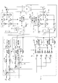
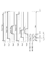
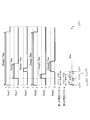
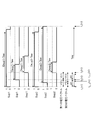
- FIG. 1 is a diagram showing an overall configuration of a control device for an AC rotating machine according to Embodiment 1 of the present invention.
- FIG. 2 is a figure for demonstrating the structure of the three-phase alternating current generator used as an alternating current rotating machine in Embodiment 1 of this invention.
- the AC rotating machine 1a shown in FIG. 1 includes the first three-phase windings U1, V1, W1 connected at the neutral point N1, and the second connected at the neutral point N2.
- the three-phase windings U2, V2, and W2 are three-phase AC rotating machines that are housed in the stator of the rotating machine without being electrically connected.
- the U1 winding and U2 winding, the V1 winding and V2 winding, and the W1 winding and W2 winding each have a phase difference of 30 degrees.
- FIG. 2 the case where both the first three-phase winding and the second three-phase winding are Y-connected is illustrated as the AC rotating machine 1a, but the present invention is also applicable to the case of ⁇ -connection. It is.
- DC power supply 2a outputs DC voltage Vdc1 to first voltage applicator 3a
- DC power supply 2b outputs DC voltage Vdc2 to second voltage applicator 3b.
- These DC power supplies 2a and 2b include all devices that output a DC voltage, such as a battery, a DC-DC converter, a diode rectifier, and a PWM rectifier.
- a configuration in which a DC voltage is output to the first voltage applicator 3a and the second voltage applicator 3b using any one of the DC power supplies 2a and 2b is also included in the scope of the present invention.
- the first voltage applicator 3a PWM modulates the first voltage commands Vu1 ′, Vv1 ′, Vw1 ′ using an inverse conversion circuit (inverter), and semiconductor switches Sup1, Sun1, Svp1, Svn1, Swp1, Swn1 (In the following description, these six semiconductor switches are expressed as semiconductor switches Sup1 to Swn1).
- the first voltage applicator 3a converts the DC voltage Vdc1 input from the DC power supply 2a into AC power, and supplies the AC voltage to the first three-phase windings U1, V1, and W1 of the AC rotating machine 1a. Apply.
- semiconductor switches Sup1 to Swn1 semiconductor switches such as IGBTs, bipolar transistors, and MOS power transistors and diodes connected in antiparallel are used.
- the second voltage applicator 3b uses the inverse conversion circuit (inverter) to PWM modulate the second voltage commands Vu2 ′, Vv2 ′, Vw2 ′, and semiconductor switches Sup2, Sun2, Svp2, Svn2, Swp2, Swn2 (In the following description, these six semiconductor switches are expressed as semiconductor switches Sup2 to Swn2). Accordingly, the second voltage applicator 3b converts the DC voltage Vdc2 input from the DC power supply 2b into AC power, and supplies the AC voltage to the second three-phase windings U2, V2, and W2 of the AC rotating machine 1a. Apply.
- semiconductor switches Sup2 to Swn2 semiconductor switches such as IGBTs, bipolar transistors, and MOS power transistors and diodes connected in antiparallel are used.
- the first current detector 4a detects the current Idc1 flowing through the first DC bus of the first power converter 3a using a current sensor such as a shunt resistor or a current transformer (CT).
- FIG. 3 is a diagram showing the relationship between the first voltage vectors V0 (1) to V7 (1) and Idc1 corresponding to the on / off states of the semiconductor switches Sup1 to Swn1 in the first embodiment of the present invention. Note that, for Sup1 to Swn1 shown in FIG. 3, “1” indicates a switch-on state and “0” indicates a switch-off state.
- the first current detector 4a detects the first three-phase currents Iu1, Iv1, and Iw1 based on the relationship shown in FIG.
- the first current detector 4a detects two phases of the first three-phase currents Iu1, Iv1, and Iw1 from Idc1, and the remaining one phase has the sum of the three-phase currents being zero. You may obtain
- the second current detector 4b detects a current Idc2 flowing through the second DC bus of the second power converter 3b using a current sensor such as a shunt resistor or a current transformer (CT).
- FIG. 4 is a diagram showing the relationship between the second voltage vectors V0 (2) to V7 (2) corresponding to the on / off states of the semiconductor switches Sup2 to Swn2 and the current equal to Idc2 in the first embodiment of the present invention. is there. Note that, for Sup2 to Swn2 shown in FIG. 4, “1” indicates a switch-on state and “0” indicates a switch-off state.
- the second current detector 4b detects the second three-phase currents Iu2, Iv2, and Iw2 based on the relationship shown in FIG.
- the second current detector 4b detects two phases of the second three-phase currents Iu2, Iv2, and Iw2 from Idc2, and the remaining one phase has the sum of the three-phase currents being zero. You may obtain
- the number (1) in parentheses in the first voltage vector shown in FIG. 3 and the number (2) in parentheses in the second voltage vector shown in FIG. (1) is attached to the first voltage vector based on the first voltage command, and the second voltage vector based on the second voltage command is ( 2) is attached.
- the first detectability determiner 12a determines whether or not the first three-phase current can be detected based on the first voltage commands Vu1 ′, Vv1 ′, and Vw1 ′, and the first detectability is determined.
- the determination signal flag_1 is output.
- the second detectability determiner 12b determines whether or not the second three-phase current can be detected based on the second voltage commands Vu2 ′, Vv2 ′, and Vw2 ′.
- a detectability determination signal flag_2 is output.
- the coordinate converter 6a converts the first three-phase currents Iu1, Iv1, Iw1 detected by the first current detector 4a into currents on rotational coordinates based on the rotational position ⁇ of the AC rotating machine 1a.
- the currents Id1 and Iq1 of the first winding on the two rotation axes are calculated.
- the coordinate converter 6b is based on a position ⁇ -30 obtained by subtracting the second three-phase currents Iu2, Iv2, Iw2 detected by the second current detector 4b from the rotational position ⁇ of the AC rotating machine 1a by 30 degrees.
- the current is converted into a current on the rotation coordinate, and the currents Id2 and Iq2 of the second winding on the two rotation axes are calculated.
- the switch 7a converts the currents Id1 and Iq1 of the first winding to the rotation biaxial coordinates, respectively. It is switched to output the currents Id1 ′ and Iq1 ′ above. Further, when it is determined that the first three-phase current cannot be detected based on the first detectability determination signal flag_1, the switch 7a rotates the currents Id2 and Iq2 of the second winding respectively. The output is switched to output currents Id1 ′ and Iq1 ′ on two-axis coordinates.
- the switch 7a supplies the currents Id2 and Iq2 of the second winding to the two rotations, respectively.
- the output is switched to output currents Id2 ′ and Iq2 ′ on the axis coordinates.
- the switch 7a rotates the currents Id1 and Iq1 of the first winding respectively.
- the output is switched to output currents Id2 ′ and Iq2 ′ on the biaxial coordinates.
- the currents Id1 ′ and Iq1 ′ on the rotating biaxial coordinates and the currents Id2 ′ and Iq2 ′ on the rotating biaxial coordinates are respectively represented by voltage commands Vd1 and Vq1 on the rotating biaxial coordinates, and This corresponds to the detected current value used to calculate the voltage commands Vd1 and Vq1 on the axis coordinates.
- the three-phase current itself of the winding on the detectable side is used as the three-phase current on the non-detectable side, but may be obtained by other estimation methods.
- the subtractor 8a calculates a deviation dId1 between the d-axis current command Id * of the AC rotating machine 1a and the current Id1 'on the rotating biaxial coordinates output from the switch 7a.
- the subtractor 8b calculates a deviation dIq1 between the q-axis current command Iq * of the AC rotating machine 1a and the current Iq1 'on the rotating biaxial coordinates output from the switch 7a.
- the subtractor 8c calculates a deviation dId2 between the d-axis current command Id * of the AC rotating machine 1a and the current Id2 'on the rotating biaxial coordinates output from the switch 7a. Further, the subtractor 8d calculates a deviation dIq2 between the q-axis current command Iq * of the AC rotating machine 1a and the current Iq2 'on the rotating biaxial coordinates output from the switch 7a.
- the controller 9a calculates the voltage command Vd1 on the rotating biaxial coordinates so as to control the deviation dId1 to zero using a P controller or a PI controller. Further, the controller 9b calculates the voltage command Vq1 on the rotating biaxial coordinates so as to control the deviation dIq1 to zero using a P controller or a PI controller.
- controller 9c calculates the voltage command Vd2 on the rotating biaxial coordinates so as to control the deviation dId2 to zero using a P controller or a PI controller. Furthermore, the controller 9d calculates the voltage command Vq2 on the rotating biaxial coordinates so as to control the deviation dIq2 to zero using the P controller or the PI controller.
- the coordinate converter 10a converts the voltage commands Vd1 and Vq1 on the rotating biaxial coordinates into three-phase AC coordinates based on the rotational position ⁇ of the AC rotating machine 1a, and converts the first voltage commands Vu1, Vv1, and Vw1. Calculate.
- the coordinate converter 10b performs coordinate conversion to three-phase AC coordinates based on a position ⁇ -30 obtained by subtracting the voltage commands Vd2 and Vq2 on the rotating biaxial coordinates from the rotation position ⁇ of the AC rotating machine 1a by 30 degrees, Second voltage commands Vu2, Vv2, and Vw2 are calculated.
- the offset calculator 11a adds the offset voltage Voffset1 to the first voltage commands Vu1, Vv1, and Vw1, as shown in the following equations (1) to (3), and the first voltage commands Vu1 ′, Vv1. Output as ', Vw1'.
- Vu1 ′ Vu1 + Voffset1 (1)
- Vv1 ′ Vv1 + Voffset1 (2)
- Vw1 ′ Vw1 + Voffset1 (3)
- the offset calculator 11b adds the offset voltage Voffset2 to the second voltage commands Vu2, Vv2, and Vw2, as shown in the following equations (4) to (6), and the second voltage commands Vu2 ′, Vv2 Output as ', Vw2'.
- Vu2 ′ Vu2 + Voffset2
- Vv2 ′ Vv2 + Voffset2
- Vw2 ′ Vw2 + Voffset2 (6)
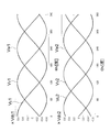
- FIG. 5 shows the first voltage command vector V1 * based on the first voltage commands Vu1 ′, Vv1 ′, Vw1 ′ and the second voltage commands Vu2 ′, Vv2 ′, Vw2 in the first embodiment of the present invention. It is explanatory drawing which showed 2nd voltage command vector V2 * based on '. As shown in FIG. 5, each of the first voltage command vector V1 * and the second voltage command vector V2 * is represented by the U (1) -V (1) -W (1) axis, U (2) -V (2) A vector that rotates the -W (2) axis.
- the numbers in parentheses shown in FIG. 5 are for separately indicating the axis corresponding to the first winding and the axis corresponding to the second winding.
- U (1), V (1), and W (1) with (1) indicate axes corresponding to the U-phase, V-phase, and W-phase of the first winding, respectively.
- U (2), V (2), and W (2) marked with (2) indicate axes corresponding to the U-phase, V-phase, and W-phase of the second winding, respectively.
- the phase angle between the first voltage command vector V1 * and the second voltage command vector V2 * with respect to the U (1) axis is ⁇ v, and there is no phase difference.
- FIG. 6 is a waveform diagram of the first voltage commands Vu1, Vv1, Vw1 and the second voltage commands Vu2, Vv2, Vw2 in the first embodiment of the present invention.
- the U (2), V (2), and W (2) axes shown in FIG. 5 are delayed by 30 degrees with respect to the U (1), V (1), and W (1) axes, respectively. Therefore, as shown in FIG. 6, the second voltage commands Vu2, Vv2, and Vw2 are delayed in phase by 30 degrees compared to the first voltage commands Vu1, Vv1, and Vw1.
- the horizontal axis represents the voltage phase angle ⁇ v with respect to the U (1) axis. Therefore, for the AC rotating machine 1a having a phase difference of 30 degrees between the first winding and the second winding, the first voltage command and the second voltage command have a phase difference of 30 degrees. Similarly, for an AC rotating machine having a phase difference of 30 + 60 ⁇ N (N: integer) degrees in the first winding and the second winding, the first voltage command and the second voltage command are: It has a phase difference of 30 + 60 ⁇ N degrees.
- FIG. 7 is a diagram for explaining the relationship between the voltage command and the rate at which each phase upper arm element is turned on with respect to the first voltage applicator 3a according to the first embodiment of the present invention.
- FIG. 7A shows the first voltage commands Vu1, Vv1, and Vw1 shown in FIG. 6, and is the output of the coordinate converter 10a.
- FIG. 7B shows the first voltage commands Vu1 ', Vv1' and Vw1 'which are the outputs of the offset calculator 11a, which are calculated by the above equations (1) to (3).
- Voffset1 in the above equations (1) to (3) is given by the following equation (7) using the maximum value Vmax1 and the minimum value Vmin1 of the first voltage commands Vu1, Vv1, and Vw1.
- Voffset1 ⁇ 0.5 (Vmin1 + Vmax1) (7)
- the voltage output range of the phase voltage that can be output by the first voltage applicator 3a is 0 to the bus voltage Vdc1. Therefore, the first voltage commands Vu1 ′, Vv1 ′, and Vw1 ′ are less than ⁇ 0.5 Vdc1 and 0.5 Vdc1 so that the width of the voltage output range is within Vdc1 that can be output by the first voltage applicator 3a. In the case of exceeding, it is limited to -0.5Vdc1 and 0.5Vdc1, respectively.
- Voffset1 In addition to the above equation (7), other offset voltage calculation methods known as a two-phase modulation method and a third harmonic superposition method may be used as Voffset1.
- FIG. 7C shows on-duty Dsup1, Dsvp1, and Dswp1 that indicate the ratios at which the upper arm elements (Sup1, Svp1, and Swp1) are turned on in the first voltage applicator 3a.
- These on-duty Dsup1, Dsvp1, and Dswp1 are respectively calculated by using Vu1 ′, Vv1 ′, and Vw1 ′.
- Dsxp1 0.5 + Vx1 ′ / Vdc1 Ask more.
- x U, V, W.
- the first voltage applicator 3a sets the ON ratio of Sup1 to 0.6 in the switching period Tsw.
- FIG. 8 is a diagram for explaining the relationship between the voltage command and the rate at which each phase upper arm element is turned on with respect to the second voltage applicator 3b in the first embodiment of the present invention.
- FIG. 8A shows the second voltage commands Vu2, Vv2, and Vw2 shown in FIG. 6, and is an output of the coordinate converter 10b.
- FIG. 8B shows the second voltage commands Vu2 ', Vv2', and Vw2 'that are the outputs of the offset calculator 11b, which are calculated by the above equations (4) to (6).
- the voltage output range of the phase voltage that can be output by the second voltage applicator 3b is 0 to the bus voltage Vdc2. Accordingly, the second voltage commands Vu2 ′, Vv2 ′, and Vw2 ′ are less than ⁇ 0.5 Vdc2 and 0.5 Vdc2 so that the width of the voltage output range is within Vdc2 that can be output by the second voltage applicator 3b. In the case of exceeding, it is limited to -0.5Vdc2 and 0.5Vdc2, respectively.
- Voffset2 in addition to the above equation (11), another offset voltage calculation method known as a two-phase modulation method or a third harmonic superposition method may be used.
- FIG. 8C shows on-duty Dsup2, Dsvp2, and Dswp2 indicating the ratios of the upper arm elements (Sup2, Svp2, and Swp2) that are turned on in the second voltage applicator 3b.
- These on-duty Dsup2, Dsvp2, and Dswp2 are respectively calculated by using Vu2 ′, Vv2 ′, and Vw2 ′.
- Dsxp2 0.5 + Vx2 ′ / Vdc2 Ask more.
- x U, V, W.
- the first voltage applicator 3a sets the ON ratio of Sup1 to 0.6 in the switching period Tsw.
- FIG. 9 is an operation explanatory diagram regarding the on / off pattern of the semiconductor switch and the current detection timing in the current detectors 4a and 4b in the first embodiment of the present invention.
- the on / off pattern of the semiconductor switches Sup1, Svp1, Swp1 of the first voltage applicator 3a and the semiconductor switches Sup2, Svp2, Swp2 of the second voltage applicator 3b, and the current detectors 4a, 4b It is the figure which showed the relationship with the electric current detection timing within the period (PWM period) Tsw of a switching signal.
- Sup1 and Sup2 are set to 1, and Svp1, Swp1, Svp2, and Swp2 are set to 0, and continues from time t1 (n) to time t2 (n) after ⁇ t1 has elapsed. 3 and 4, from time t1 (n) to t2 (n), the first voltage vector is V1 (1) and the second voltage vector is V1 (2).
- the current detectors 4a and 4b detect Idc1 and Idc2 at time ts1-1 (n) from time t1 (n) to t2 (n).
- the dead time time of the first voltage applicator 3a or the second voltage applicator 3b and the time required for the first current detector to detect Idc1 or the second current detector to detect Idc2 (for example, when the sum of the time required for the ringing included in the detected waveform to converge and the time required for the sample hold is “first predetermined value”, the shift time ⁇ t1 is equal to or greater than the “first predetermined value”.
- the first voltage vector is V1 (1), and Idc1 detected at time ts1-1 (n) is equal to Iu1.
- the second voltage vector is V1 (2), and Idc2 detected at time ts1-1 (n) is equal to Iu2.
- Svp1 and Svp2 are set to 1, and the switching pattern is continued from time t2 (n) until time t3 (n) after ⁇ t2. 3 and 4, from time t2 (n) to t3 (n), the first voltage vector is V2 (1) and the second voltage vector is V2 (2).
- Current detector 4a. 4b detects Idc1 and Idc2 again at time ts1-2 (n) from time t2 (n) to t3 (n).
- the shift time ⁇ t2 is set to be not less than the “first predetermined value” similarly to the shift time ⁇ t1.
- the first voltage vector is V2 (1), and Idc1 detected at time ts1-2 (n) is equal to ⁇ Iw1.
- the second voltage vector is V2 (2), and Idc2 detected at time ts1-2 (n) is ⁇ Iw2. equal.
- Swp1 and Swp2 are set to 1 at time t3 (n).
- the pulse widths of Sup1 to Swp2 are determined by the multiplied value of the on-duty Dsup1, Dswp2 and the switching period Tsw corresponding to each switch.
- the switch of the upper arm element of the phase corresponding to the first maximum phase voltage Emax1 the switch of the upper arm element of the phase corresponding to the first intermediate phase voltage Emid1, the first minimum phase voltage Emin1.
- the switch of the upper arm element of the phase corresponding to the first maximum phase voltage Emax1 the switch of the upper arm element of the phase corresponding to the first intermediate phase voltage Emid1, the first minimum phase voltage Emin1.
- two types of first voltage vectors capable of detecting two phases of the first three-phase currents Iu1, Iv1, and Iw1 are formed from Idc1 shown in FIG.
- two types of second voltage vectors that can detect two phases of the second three-phase currents Iu2, Iv2, and Iw2 are formed from Idc2.
- FIG. 10 is an operation explanatory diagram different from FIG. 9 regarding the on / off pattern of the semiconductor switch and the current detection timing in the current detectors 4a and 4b in the first embodiment of the present invention, and the first three-phase. The case where the currents Iu1, Iv1, and Iw1 cannot be detected is illustrated.
- FIG. 10 shows a state where Vv1 ′ is small and Dsvp1 ⁇ Tsw is smaller than ⁇ t2.
- Svp1 is turned on at time t2 (n)
- it is turned off before time t3 (n)
- the first voltage vector V2 (1) cannot be formed over the section of the shift time ⁇ t2.
- FIG. 11 is an operation explanatory diagram different from FIGS. 9 and 10 regarding the on / off pattern of the semiconductor switch and the current detection timing in the current detectors 4a and 4b according to the first embodiment of the present invention. In the same manner as in FIG. 3, the case where the first three-phase currents Iu1, Iv1, and Iw1 cannot be detected is illustrated.
- FIG. 11 shows a state where Vv1 ′ is large and Dsvp1 ⁇ Tsw is larger than Tsw ⁇ t1.
- Vv1 ′ is large and Dsvp1 ⁇ Tsw is larger than Tsw ⁇ t1.
- Svp1 is turned off at time t4 (n) when the switching cycle Tsw ends, if Svp1 is not turned on before time t2 (n), a pulse width corresponding to Dsvp1 ⁇ Tsw can be output. Absent.
- V1 (1) cannot be formed over the section of the shift time ⁇ t1.
- FIG. 12 is an operation explanatory diagram different from FIG. 10 and FIG. 11 regarding the on / off pattern of the semiconductor switch and the current detection timing in the current detectors 4a and 4b according to the first embodiment of the present invention.
- the case where the phase currents Iu2, Iv2, and Iw2 cannot be detected is illustrated.
- the second voltage applicator 3b cannot be formed over the interval of the shift time ⁇ t2 when Vv2 ′ is small.
- FIG. 13 is an operation explanatory diagram different from FIG. 12 regarding the on / off pattern of the semiconductor switch and the current detection timing in the current detectors 4a and 4b in the first embodiment of the present invention.
- the case where the currents Iu2, Iv2, and Iw2 cannot be detected is illustrated.
- Vv2 ' is large, V1 (2) cannot be formed over the section of the shift time ⁇ t1.
- the switching frequency when Tsw is increased, the switching frequency given by the reciprocal of Tsw decreases, and when the frequency enters the audible range, there arises a problem that noise of the switching frequency component increases.
- the switching frequency when the AC rotating machine 1a is an electric power steering motor, the switching frequency is set to 20 kHz or more (out of the audible band).
- the human audible range is 20 Hz to 20 kHz, and by setting the frequency to 20 kHz or higher (out of the audible range), the sound of the switching frequency component cannot be heard by the human ear. However, if the switching frequency is lowered below 20 kHz in order to ensure the shift time ⁇ t1 and the shift time ⁇ t2, the sound of the switching frequency component is heard by human ears, resulting in noise.
- the AC rotating machine 1a has The applied voltage is limited, and another problem arises that the AC rotating machine 1a cannot generate a high output.
- Idc1 cannot be detected depending on the magnitude of the first intermediate phase voltage Emid1
- Idc2 is detected with high accuracy, and depending on the magnitude of the second intermediate phase voltage Emid2.
- the technical feature is that Idc1 is detected with high accuracy.
- FIG. 14 is an operation explanatory diagram regarding the on / off pattern of the semiconductor switch and the current detection timing in the current detectors 4a and 4b according to the first embodiment of the present invention, and shows the operation for solving the problem in FIG. ing. Specifically, in FIG. 14, the on timing of Svp1 is shifted from t2 (n) to t5 (n) with respect to FIG.
- T5 (n) is set within the “second predetermined value” before and after the timing t3 (n) when the first minimum phase voltage is turned on.
- the “second predetermined value” is a value smaller than the “first predetermined value”
- the bus current detection timing ts1-2 (n) and the first minimum phase turn-on timing t3 (n ) Is smaller than the interval. Note that it may be set so that t3 (n) and t5 (n) coincide, that is, the first intermediate phase voltage and the first minimum phase voltage are simultaneously turned on.
- the ON time of the first intermediate phase voltage becomes a value corresponding to ⁇ t2 or less
- the ON time of the first intermediate phase voltage is set to the first time as shown in FIG.
- the on-time of the minimum phase voltage is brought closer to the second predetermined value. Accordingly, the configuration of FIG. 14 does not cause the switching of the first voltage applicator 3a in the vicinity of ts1-2 (n), and Idc2 at ts1-2 (n) is more accurately compared with FIG. It can be detected.
- FIG. 15 is an operation explanatory diagram regarding the on / off pattern of the semiconductor switch and the current detection timing in the current detectors 4a and 4b according to the first embodiment of the present invention, and shows the operation for solving the problem in FIG. ing. Specifically, in FIG. 15, the on-timing of Svp1 is shifted from t2 (n) to t6 (n) with respect to FIG.
- T6 (n) is set within the “second predetermined value” before and after the timing t1 (n) when the first maximum phase voltage is turned on. Note that t1 (n) and t6 (n) may be matched, that is, the first intermediate phase voltage and the first maximum phase voltage may be turned on simultaneously.
- the ON time of the first intermediate phase voltage becomes a value corresponding to ⁇ t2 or less
- the ON time of the first intermediate phase voltage is set to the first maximum value as shown in FIG.
- the phase voltage is brought close to the on-time of the phase voltage so as to be within a second predetermined value.
- the configuration of FIG. 15 does not cause the switching of the first voltage applicator 3a in the vicinity of ts1-1 (n), and Idc2 at ts1-1 (n) is detected more accurately than in the previous FIG. it can.
- FIG. 16 is an operation explanatory diagram different from FIG. 9 regarding the on / off pattern of the semiconductor switch and the current detection timing in the current detectors 4a and 4b in the first embodiment of the present invention.
- Sup1, Sup2, Svp1, and Svp2 are set to 1, and Swp1 and Swp2 are set to 0, and continues from time t1 (n) to time t2 (n) after ⁇ t1 has elapsed. 3 and 4, from time t1 (n) to t2 (n), the first voltage vector is V2 (1), and the second voltage vector is V2 (2).
- the current detectors 4a and 4b detect Idc1 and Idc2 at time ts1-1 (n) from time t1 (n) to t2 (n).
- the first voltage vector is V2 (1), and Idc1 detected at time ts1-1 (n) is equal to ⁇ Iw1.
- the second voltage vector is V2 (2), and Idc2 detected at time ts1-1 (n) is ⁇ Iw2. equal.
- Svp1 and Svp2 are set to 0, and the switching pattern is continued from time t2 (n) until time t3 (n) after ⁇ t2. 3 and 4, from time t2 (n) to t3 (n), the first voltage vector is V1 (1), and the second voltage vector is V1 (2).
- Current detector 4a. 4b detects Idc1 and Idc2 again at time ts1-2 (n) from time t2 (n) to t3 (n).
- the first voltage vector is V1 (1), and Idc1 detected at time ts1-2 (n) is equal to Iu1.
- the second voltage vector is V1 (2), and Idc2 detected at time ts1-2 (n) is equal to Iu2.
- Sup1 and Sup2 are set to 1 at time t3 (n).
- the time for which Sup1 to Swp2 continues to be “0” is determined by the product of the value obtained by subtracting the on-duty Dsup1, Dswp2 corresponding to each switch from 1 and the switching cycle Tsw.
- the switch of the upper arm element of the phase corresponding to the first minimum phase voltage Emim1 the switch of the upper arm element of the phase corresponding to the first intermediate phase voltage Emid1
- the time is shifted off by ⁇ t1 and ⁇ t2 set to the first predetermined value or more.
- two types of first voltage vectors capable of detecting two phases of the first three-phase currents Iu1, Iv1, and Iw1 are formed from Idc1 shown in FIG.
- two types of second voltage vectors that can detect two phases of the second three-phase currents Iu2, Iv2, and Iw2 are formed from Idc2.
- FIG. 17 is an operation explanatory diagram different from FIG. 16 regarding the ON / OFF pattern of the semiconductor switch and the current detection timing in the current detectors 4a and 4b in the first embodiment of the present invention, and the first three-phase. The case where the currents Iu1, Iv1, and Iw1 cannot be detected is illustrated.
- FIG. 17 shows a state where Vv1 ′ is small and Dsvp1 ⁇ Tsw is smaller than ⁇ t1.
- Svp1 is turned on at time t1 (n)
- it is turned off before time t2 (n)
- the first voltage vector V2 (1) cannot be formed over the section of the shift time ⁇ t1.
- ⁇ dc1 cannot be detected in the ⁇ t1 interval.
- the off timing of Svp1 is between t1 (n) and t2 (n), and the interval with ts1-1 (n), which is the timing for detecting Idc2, approaches. For this reason, there is a possibility that detection noise occurs in Idc2 due to switching that turns off Svp1, and Idc2 cannot be detected correctly in the ⁇ t2 interval.
- FIG. 18 is an operation explanatory diagram different from FIGS. 16 and 17 regarding the on / off pattern of the semiconductor switch and the current detection timing in the current detectors 4a and 4b according to the first embodiment of the present invention. As in FIG. 17, the case where the first three-phase currents Iu1, Iv1, Iw1 cannot be detected is illustrated.
- FIG. 17 shows a state where Vv1 ′ is large and Svp1 off time (1-Dsvp1) ⁇ Tsw is smaller than ⁇ t2.
- Svp1 is turned off at time t2 (n)
- it is turned on before time t3 (n).
- the first vector V1 (1) is shifted by ⁇ t2. Cannot be formed over the interval of Idc1, and Idc1 cannot be detected in the interval of ⁇ t2.
- the on timing of Svp1 is between t2 (n) and t3 (n), and the interval with ts1-2 (n), which is the timing for detecting Idc2, approaches. For this reason, there is a possibility that detection noise occurs in Idc2 due to switching that turns on Svp1, and Idc2 cannot be detected correctly in the ⁇ t2 interval.
- FIG. 19 is an operation explanatory diagram different from FIGS. 17 and 18 regarding the ON / OFF pattern of the semiconductor switch and the current detection timing in the current detectors 4a and 4b according to the first embodiment of the present invention.
- the case where the phase currents Iu2, Iv2, and Iw2 cannot be detected is illustrated.
- Vv2 ′ is small
- V2 (2) cannot be formed over the section of the shift time ⁇ t1, and Idc2 cannot be detected in the ⁇ t1 section. .
- the off timing of Svp2 is between t1 (n) and t2 (n), and the interval with ts1-1 (n), which is the timing for detecting Idc1, approaches. For this reason, there is a possibility that detection noise occurs in Idc1 due to switching that turns off Svp2, and Idc1 cannot be detected correctly in the ⁇ t1 interval.
- FIG. 20 is an operation explanatory diagram different from FIG. 19 regarding the on / off pattern of the semiconductor switch and the current detection timing in the current detectors 4a and 4b in the first embodiment of the present invention.
- the case where the currents Iu2, Iv2, and Iw2 cannot be detected is illustrated.
- Vv2 'is large V1 (2) cannot be formed over the interval of the shift time ⁇ t2, and Idc2 cannot be detected in the ⁇ t2 interval.
- the on timing of Svp2 is between t2 (n) and t3 (n), and the interval with ts1-2 (n), which is the timing for detecting Idc1, approaches. For this reason, there is a possibility that detection noise is generated in Idc1 due to switching that turns on Svp2, and Idc1 cannot be detected correctly in the ⁇ t2 section.
- FIG. 21 is an operation explanatory diagram regarding the on / off pattern of the semiconductor switch and the current detection timing in the current detectors 4a and 4b according to the first embodiment of the present invention, and shows the operation for solving the problem in FIG. ing. Specifically, in FIG. 21, the Svp1 off timing is shifted to t7 (n) with respect to FIG.
- T7 (n) is set within the “second predetermined value” before and after the timing t4 (n) when the first minimum phase voltage is turned off. In this manner, the off time of the first intermediate phase voltage is brought close to the off time of the first minimum phase voltage within the second predetermined value. As a result, the configuration of FIG. 21 does not cause the switching of the first voltage applicator 3a in the vicinity of ts1-1 (n), and Idc2 at ts1-1 (n) is more accurately compared with FIG. It can be detected.
- FIG. 22 is an operation explanatory diagram regarding the on / off pattern of the semiconductor switch and the current detection timing in the current detectors 4a and 4b according to the first embodiment of the present invention, and shows the operation for solving the problem in FIG. ing. Specifically, in FIG. 22, the Svp1 off timing is shifted to t8 (n) with respect to FIG.
- T8 (n) is set within the “second predetermined value” before and after the timing t3 (n) when the first maximum phase voltage is turned on. In this way, the OFF time of the first intermediate phase voltage is brought close to the OFF time of the first maximum phase voltage so as to be within the second predetermined value.
- the switching of the first voltage applicator 3a does not occur in the vicinity of ts1-2 (n), and Idc2 at ts1-2 (n) is detected more accurately than in the previous FIG. it can.
- FIG. 23 is an explanatory diagram regarding the functions of the first detectability determiner 12a and the second detectability determiner 12b according to Embodiment 1 of the present invention.
- the first current availability determination unit 12a determines whether the voltage command value of the phase corresponding to the first intermediate phase voltage Emid1 is in the range of the third predetermined value Vs3 or less and the fourth predetermined value Vs4 or more. It is determined whether the first current detector 4a can detect the first three-phase current.
- the second current availability determination unit 12b determines whether or not the voltage command value of the phase corresponding to the second intermediate phase voltage Emid2 is in the range of the third predetermined value Vs3 or less and the fourth predetermined value Vs4 or more. It discriminate
- the third predetermined value Vs3 corresponds to an upper limit value that can secure the shift time ⁇ t1.
- the fourth predetermined value Vs4 is a lower limit value that can ensure the shift time ⁇ t2.
- FIG. 23A shows the first voltage commands Vu1 ′, Vv1 ′, Vw1 ′ shown in FIG. 7B as dotted lines, the first intermediate phase voltage Emid1 as a solid line, the third predetermined value Vs3 and the fourth The predetermined value Vs4 is indicated by a one-dot chain line.
- Vs3 0.4Vdc1
- Vs4 ⁇ 0.4Vdc1 Set to.
- FIG. 23B shows the output of the first detectability determiner 12a.
- the first detectability determiner 12a determines whether the first intermediate phase voltage Emid1 is within or outside the third predetermined value Vs3 or less and the fourth predetermined value Vs4 or more. It is determined whether or not the phase current can be detected.
- the first detectability determiner 12a is 1 if the first intermediate phase voltage Emid1 is within the range of the third predetermined value Vs3 or less and the fourth predetermined value Vs4 or more, and 0 if it is out of range.
- the first detection availability determination signal flag_1 is output.
- FIG. 23C shows the second voltage commands Vu2 ′, Vv2 ′ and Vw2 ′ shown in FIG. 8B as dotted lines, the second intermediate phase voltage Emid2 as a solid line, the third predetermined value Vs3 and the fourth The predetermined value Vs4 is indicated by a one-dot chain line.
- FIG. 23 (d) shows the output of the second detectability determiner 12b.
- the second detectability determiner 12b determines whether the second intermediate phase voltage Emid2 is within the range of the third predetermined value Vs3 or less and the fourth predetermined value Vs4 or more, or out of the range. It is determined whether or not the phase current can be detected, and if the phase current is within the range of the third predetermined value Vs3 or less and the fourth predetermined value Vs4 or more, the value is 1;
- the signal flag_2 is output.
- the voltage phase angle ⁇ v becomes 0 in the vicinity of 60 ⁇ x (x: 0, 1, 2, 3, 4, 5, 6) degrees.
- the voltage phase angle ⁇ v becomes 0 near 30 + 60 ⁇ x (x: 0, 1, 2, 3, 4, 5) degrees.
- the voltage phase angle ⁇ v that becomes 0 is shifted from each other by 30 degrees, and when the flag_1 is 0, the flag_2 is 1 and vice versa.
- flag_1 is 1. Therefore, it can be seen that flag_1 and flag_2 are not 0 simultaneously, and at least one is 1.
- FIG. 24 is a flowchart showing a series of operations of the first detectability determiner 12a in the first embodiment of the present invention.
- the first detectability determiner 12a calculates the first intermediate phase voltage Emid1 based on the first voltage commands Vu1 ', Vv1', Vw1 '.
- step S1000b the first detectability determiner 12a determines whether or not the first intermediate phase voltage Emid1 is equal to or lower than a third predetermined value Vs3. If “YES”, the process proceeds to step S1000c. If “NO”, the process proceeds to step S1000e.
- the first detectability determiner 12a determines whether or not the first intermediate phase voltage Emid1 is equal to or higher than the fourth predetermined value Vs4. The process proceeds to S1000d, and if “NO”, the process proceeds to Step S1000e.
- the first detectability determination unit 12a substitutes 1 for the first detectability determination signal flag_1.
- the first detection availability determination unit 12a substitutes 0 for the first detection availability determination signal flag_1.
- FIG. 25 is a flowchart showing a series of operations of the second detectability determiner 12b in the first embodiment of the present invention.
- the second detectability determiner 12b calculates the second intermediate phase voltage Emid2 based on the second voltage commands Vu2 ', Vv2', Vw2 '.
- step S2000b the second detectability determiner 12b determines whether or not the second intermediate phase voltage Emid2 is equal to or lower than a third predetermined value Vs3. If “YES”, the process proceeds to step S2000c. If “NO”, the process proceeds to step S2000e.
- step S2000c the second detectability determiner 12b determines whether or not the second intermediate phase voltage Emid2 is equal to or higher than a fourth predetermined value Vs4. If “YES”, the process proceeds to step S2000d. If “NO”, the process proceeds to step S2000e.
- step S2000d the second detectability determination unit 12b substitutes 1 for the second detectability determination signal flag_2.
- step S2000e the second detectability determination unit 12b substitutes 0 for the second detectability determination signal flag_2.
- FIG. 26 is a flowchart showing a series of operations of switch 7a in the first embodiment of the present invention.
- the switching operation by the switching unit 7a is performed by determining whether or not the first detection possibility determination signal flag_1 in step S3100a is equal to 1, and whether or not the second detection possibility determination signal flag_2 in step S3100b is equal to 1.
- the process is divided into steps S3100c, 3100d, and 3100e.
- step S3100c the currents Id1 and Iq1 of the first winding are selected as Id1 ′ and Iq1 ′, and the second current is set as Id2 ′ and Iq2 ′.
- the winding currents Id2 and Iq2 are selected and output.
- step S3100d the currents Id1 and Iq1 of the first winding are selected as Id1 ′ and Iq1 ′, and Id2 ′ and Iq2 ′ are also selected.
- the currents Id1 and Iq1 of the first winding are selected and output.
- step S3100e When flag_1 is not equal to 1, regardless of the value of flag_2, the process proceeds to step S3100e, and currents Id2 and Iq2 of the second winding are selected as Id1 ′ and Iq1 ′, and Id2 ′ and Iq2 ′ are also selected. The currents Id2 and Iq2 of the second winding are selected and output.
- the present invention is also useful when a voltage is applied at an off-interval greater than or equal to the first predetermined value.
- the first intermediate phase voltage when the first intermediate phase voltage is larger than the first predetermined value, the first intermediate phase voltage is set to the first maximum phase voltage and the second maximum voltage.
- An example of changing to turn on at a timing within a predetermined value of has been described.
- the first minimum phase voltage may also be changed to turn on at a timing within the first maximum phase voltage and the second predetermined value.
- all three phases of the voltage applied to the first three-phase winding are turned on within the second predetermined value. Therefore, according to the present invention, with respect to at least two phases of the first three-phase winding or the second three-phase winding for which current detection is determined to be impossible, the on or off interval is within the second predetermined value. The effect can be obtained by setting.
- the first intermediate phase voltage is in a range in which the shift time can be secured without increasing the switching cycle Tsw as in Patent Document 1.
- Embodiment 2 In the control device for an AC rotating machine according to the second embodiment, the calculation process in the first detectability determiner 12c is different from the first detectability determiner 12a in the first embodiment. Therefore, the following description will focus on the arithmetic processing of the first detectability determiner 12c in the second embodiment.
- FIG. 27 is a flowchart showing a series of operations of the first detectability determiner 12c in the second embodiment of the present invention.
- the first detectability determiner 12c determines the first maximum phase voltage Emax1, the first intermediate phase voltage Emid1, the first minimum phase voltage based on the first voltage commands Vu1 ′, Vv1 ′, Vw1 ′. Emin1 is calculated.
- step S4000b the first detectability determiner 12c determines whether or not the difference between the first maximum phase voltage and the first intermediate phase voltage (Emax1 ⁇ Emid1) is equal to or greater than a fifth predetermined value Vs5. If “YES”, the process proceeds to step S4000c, and if “NO”, the process proceeds to step S4000e.
- the first detectability determiner 12c determines whether the difference (Emid1-Emin1) between the first intermediate phase voltage and the first minimum phase voltage is equal to or greater than the fifth predetermined value Vs5. If “YES”, the process proceeds to step S4000d, and if “NO”, the process proceeds to step S4000e.
- the first detection availability determination unit 12c substitutes 1 for the first detection availability determination signal flag_1.
- the first detection availability determination unit 12c substitutes 0 for the first detection availability determination signal flag_1.
- FIG. 28 is a diagram showing waveforms corresponding to the respective steps in FIG. 27 when the fifth predetermined value Vs5 in the second embodiment of the present invention is set to 0.1 Vdc.
- FIG. 28A shows waveforms of the first voltage commands Vu1 ', Vv1', and Vw1 '.
- FIG. 28B shows waveforms of the first maximum phase voltage Emax1, the first intermediate phase voltage Emid1, and the first minimum phase voltage Emin1 corresponding to step S4000a.
- FIG. 28 (c) shows a difference Emax1-Emid1 between the first maximum phase voltage and the first intermediate phase voltage corresponding to step S4000b, and a difference between the first intermediate phase voltage and the first minimum phase voltage corresponding to step S4000c.
- FIG. 28 (d) shows the waveform of the first detectability determination signal flag_1 corresponding to steps S4000d and S4000e.
- the difference between the first maximum phase voltage and the first intermediate phase voltage and the difference between the first intermediate phase voltage and the first minimum phase voltage are calculated, and those values are the fifth. Even when it is determined that the first three-phase current cannot be detected when the value is less than the predetermined value, the same effect as in the first embodiment can be obtained.
- the first detectability determiner 12c Based on the first voltage commands Vu1 ′, Vv1 ′, and Vw1 ′ that are the outputs of the offset calculator 11a, the first detectability determiner 12c generates the first three-phase current. Judgment was made on whether or not detection was possible. However, even if the first voltage commands Vu1, Vv1, and Vw1 that are the inputs of the offset calculator 11a are substituted for the first voltage commands Vu1 ′, Vv1 ′, and Vw1 ′ and calculated, Emax1 ⁇ Emid1 and The calculation result of Emid1-Emin1 is the same.
- the configuration is the same as the case of calculating based on the first voltage commands Vu1 ′, Vv1 ′, and Vw1 ′. The effect is obtained.
- the second detectability determiner 12b uses the second voltage commands Vu2 ′, Vv2 ′, and Vw2 ′ and uses the second voltage commands Vu2 ′, Vv2 ′, and the first detectability determiner 12c in FIG. It goes without saying that the second detection possibility determination signal flag_2 is obtained by performing the calculation.
- Embodiment 3 In the control device for an AC rotating machine according to the third embodiment, the calculation process in the first detectability determiner 12d is different from the first detectability determiner 12a in the first embodiment. Therefore, the following description will be focused on the arithmetic processing of the first detectability determiner 12d in the third embodiment.
- the first detectability detector 12d in the present third embodiment calculates the voltage phase angle ⁇ v by the following equation (21) based on the first voltage commands Vu1 ′, Vv1 ′, Vw1 ′, and the voltage phase Whether or not the first three-phase current can be detected is determined according to the region of the angle ⁇ v.
- the first three-phase current cannot be detected when the voltage phase angle ⁇ v is around 60 ⁇ x (x: 0, 1, 2, 3, 4, 5, 6) degrees. Indicated. Therefore, the first detectability determiner 12d determines that ⁇ v obtained by calculation based on the first voltage command is in the range of 60 ⁇ x ⁇ to 60 ⁇ x + ⁇ (where ⁇ is a margin). Is determined to be undetectable, and 0 is output as flag_1. If it is out of the range, it is determined to be detectable and 1 is output as flag_1.
- the margin ⁇ is determined by the shift times ⁇ t1, ⁇ t2, the maximum value of the first voltage command, etc., but is within 30 degrees.
- the same determination as in the first embodiment can be made by determining whether or not the first three-phase current can be detected according to the voltage phase angle of the first voltage command. An effect can be obtained.
- the second three-phase current cannot be detected in the vicinity of 30 + 60 ⁇ x (x: 0, 1, 2, 3, 4, 5) degrees at the voltage phase angle ⁇ v. Indicated. Therefore, the second detectability determiner 12d determines that ⁇ v obtained by the calculation based on the first voltage command is in the range of 30 + 60 ⁇ x ⁇ to 30 + 60 ⁇ x + ⁇ ( ⁇ : margin). It may be determined that detection is impossible, 0 is output as flag_2, and when it is out of the range, it is determined that detection is possible and 1 is output as flag_2.
- the first detectability determiner 12d determines the first three-phase current based on the first voltage commands Vu1 ′, Vv1 ′, and Vw1 ′ that are the outputs of the offset calculator 11a. Judgment was made on whether or not detection was possible. However, even if the first voltage commands Vu1, Vv1, and Vw1 that are the inputs of the offset calculator 11a are substituted for the first voltage commands Vu1 ′, Vv1 ′, and Vw1 ′ and calculated, the above formula (21 ) Result is the same.
- the configuration is the same as the case of calculating based on the first voltage commands Vu1 ′, Vv1 ′, and Vw1 ′. The effect is obtained.
- the first three phases are obtained based on the voltage phase angle ⁇ v. All methods of determining whether or not current can be detected or whether or not the second three-phase current can be detected are included in the present invention.
- the first detectability determiner 12d uses the second voltage commands Vu2 ′, Vv2 ′, and Vw2 ′ instead of the first voltage commands Vu1, Vv1, and Vw1, and uses the second equation (22) It is also possible to obtain the phase angle ⁇ v.
- the voltage phase angle ⁇ v can be calculated using the first voltage commands Vu2, Vv2, Vw2 and the rotary biaxial voltage commands Vd2, Vq2.
- FIG. FIG. 29 is a diagram showing an overall configuration of an AC generator control device according to Embodiment 4 of the present invention.
- the configuration of the fourth embodiment is different from the configuration of the first embodiment in that a control unit 5b is used instead of the control unit 5a. Therefore, the control unit 5b will be described below with a focus on the changes from the control unit 5a.
- the adder 801a outputs an addition value (Id1 ′ + Id2 ′) of the current Id1 ′ on the two rotation axes and the current Id2 ′ on the two rotation axes.
- the adder 801b outputs an addition value (Iq1 ′ + Iq2 ′) of the current Iq1 ′ on the two rotation axes and the current Iq2 ′ on the two rotation axes.
- the subtractor 802a outputs a value (Id1′ ⁇ Id2 ′) obtained by subtracting the current Id1 ′ on the two rotation axes by the current Iq2 ′ on the two rotation axes.
- the subtractor 802b outputs a value (Iq1′ ⁇ Iq2 ′) obtained by subtracting the current Iq1 ′ on the two rotation axes by the current Iq2 ′ on the two rotation axes.
- the multiplier 803a multiplies the addition value (Id1 ′ + Id2 ′) output from the adder 801a by K1, and outputs the sum as a sum current Id_sum.
- K1 is 0.5.
- the multiplier 803b multiplies the added value (Iq1 ′ + Iq2 ′) output from the adder 801b by K1, and outputs a sum current Iq_sum.
- K1 is 0.5.
- the multiplier 804a multiplies the subtraction value (Id1′ ⁇ Id2 ′) output from the subtractor 802a by K2, and outputs a difference current delta_Id.
- K2 is 0.5.
- the multiplier 804b multiplies the subtraction value (Iq1′ ⁇ Iq2 ′) output from the subtractor 802b by K2, and outputs a difference current delta_Iq.
- K2 is 0.5.
- the subtractor 805a calculates a deviation dId_sum between the d-axis current command Id * and the sum current Id_sum of the AC rotating machine 1a.
- the subtractor 805b calculates a deviation dIq_sum between the q-axis current command Iq * of the AC rotating machine 1a and the sum current Iq_sum.
- the controller 806a outputs a sum voltage Vd_sum so as to control the deviation dId_sum to zero based on the product of the proportional gain Kpd_sum and the deviation dId_sum of the controller using a P controller, a PI controller, or the like. .
- the controller 806b outputs the sum voltage Vd_sum using a P controller, a PI controller, or the like so as to control the deviation dIq_sum to zero based on the product of the proportional gain Kpq_sum and the deviation dIq_sum of those controllers. .
- the controller 806c uses a P controller, a PI controller, or the like to output the difference voltage delta_Vd so as to control the difference current delta_Id to zero based on the multiplication value of the proportional gain Kpd_delta and the deviation delta_dId of the controllers. To do.
- the controller 806d uses a P controller, a PI controller, or the like to output the difference voltage delta_Vq so as to control the difference current delta_Iq to zero based on the multiplication value of the proportional gain Kpq_delta and the deviation delta_dIq of those controllers. To do.
- the adder 807a outputs a value obtained by adding the sum voltage Vd_sum and the difference voltage delta_Vd as the first voltage command Vd1.
- the adder 807b outputs a value obtained by adding the sum voltage Vq_sum and the difference voltage delta_Vq as the first voltage command Vq1.
- the subtractor 808a outputs a value obtained by subtracting the sum voltage Vd_sum by the difference voltage delta_Vd as the second voltage command Vd2.
- the subtractor 808a outputs a value obtained by subtracting the sum voltage Vq_sum by the difference voltage delta_Vq as the second voltage command Vq2.
- both the first detectability determination signal flag_1 and the second detectability determination signal flag_2 are 1 (that is, when it is determined that both the first three-phase current and the second three-phase current can be detected).
- the currents Id1 ′ and Iq1 ′ on the two rotating axes are equal to the currents Id1 and Iq1 of the first winding, and the currents Id2 ′ and Iq2 ′ on the rotating two axes are the currents Id2 and Iq2 of the second winding. equal.
- the sum current is represented by the sum of the first three-phase current detected by the first current detector 4a and the second three-phase current detected by the second current detector 4b.
- the current is represented by a difference between the first three-phase current detected by the first current detector 4a and the second three-phase current detected by the second current detector 4b.
- Sum voltages Vd_sum and Vq_sum are calculated based on the sum currents Id_sum and Iq_sum and the sum current gain, and difference voltages delta_Vd and delta_Vq are calculated based on the difference currents delta_Id and delta_Iq and the difference current gain. Further, the first voltage commands Vd1 and Vq1 and the second voltage commands Vd2 and Vq2 are calculated by the adders 807a and 807b and the subtracters 808a and 808b.
- the first three-phase windings U1, V1, and W1 of the AC rotating machine 1a and the second three-phase windings U2, V2, and W2 are not electrically connected but are magnetically coupled to each other. Has been. Therefore, a voltage proportional to the product of the differential value of the first three-phase current and the mutual inductance between the first and second windings is generated in the second three-phase winding. On the other hand, a voltage proportional to the product of the differential value of the second three-phase current and the mutual inductance between the first and second windings is generated in the first three-phase winding. That is, the first winding and the second winding are magnetically interfering with each other.
- the first voltage commands Vd1 and Vq1 and the second voltage commands Vd2 and Vq2 are calculated based on the sum current and the difference current.
- the voltage commands Vd1 and Vq1 of the first winding are the first detected by the first current detector 4a.
- the second three-phase current detected by the second current detector 4b is also taken into consideration.
- the second voltage commands Vd2 and Vq2 are the first three detected by the first current detector 4a.
- the calculation is performed in consideration of the phase current. Therefore, by providing the configuration of the fourth embodiment, a more stable control system can be constructed against magnetic interference between the first winding and the second winding.
- the currents Id1 ′ and Iq1 ′ on the rotating two axes are equal to the currents Id1 and Iq1 of the first winding, as shown in FIG.
- Currents Id2 ′ and Iq2 ′ are also equal to the currents Id2 and Iq2 of the second winding.
- the sum current is represented by the second three-phase current detected by the second current detector 4b, and the difference current is zero. Therefore, the first voltage commands Vd1, Vq1, and the second voltage commands Vd2, Vq2 are calculated based on the second three-phase current and the sum current gain.
- the currents Id1 ′ and Iq1 ′ on the two rotating axes are equal to the currents Id1 and Iq1 of the first winding, as shown in FIG.
- the upper currents Id2 ′ and Iq2 ′ are also equal to the currents Id1 and Iq1 of the first winding.
- the sum current is represented by the first three-phase current detected by the first current detector 4a, and the difference current is zero. Therefore, the first voltage commands Vd1, Vq1, and the second voltage commands Vd2, Vq2 are calculated based on the first three-phase current and the sum current gain.
- the second detectability determiner 12b When the first detectability determiner 12a outputs 0 as flag_1, the second detectability determiner 12b outputs 0 as flag_2 from the above equations (29) and (30). In this case, the difference current is set to 0 from the above equations (33) and (34). For this reason, the difference voltage obtained by multiplying the difference current by the difference voltage gain is also zero.
- the subtracters 802a and 802b, the multipliers 804a and 804b, and the controllers 806c and 806d until the difference voltages delta_Vd and delta_Vq are set to 0 and the difference voltage is calculated from the difference current may be omitted.
- the three-phase current itself of the winding on the detectable side is used as the three-phase current on the non-detectable side, but may be obtained by other estimation methods.
- the first detection possibility determination is made by changing the difference current gains Kpd_delta and Kpq_delta based on at least one of the first voltage command, the second voltage command, the sum voltage, or the rotational speed of the AC rotating machine 1a. It is possible to reduce the pulsation to the differential voltages delta_Vd and delta_Vq due to the pulsation of the difference currents delta_Id and delta_Iq when the signal flag_1 and the second detection possibility determination signal flag_2 are switched from 0 to 1 or 1 to 0.
- FIG. 30 is a diagram showing a state in which the differential current gain is varied based on the first voltage command in the fourth embodiment of the present invention.
- FIG. 30 illustrates a case where the differential current gains Kpd_delta and Kpq_delta are changed according to the amplitude V1 of the first voltage command.
- the differential current gains Kpd_delta and Kpq_delta are set to constant values as Kpd_delta1 and Kpq_delta1, respectively.
- the amplitude V1 of the first voltage command when the amplitude V1 of the first voltage command is greater than the threshold value Vsa1, the differential current gains Kpd_delta and Kpq_delta are respectively reduced on a straight line.
- the threshold value Vsa1 and the slope of the straight line may be determined according to the generated pulsation level.
- the amplitude V1 of the first voltage command may be obtained by the following equation (35).
- the horizontal axis of FIG. 30 can be set to the square of the amplitude.
- the horizontal axis of FIG. 30 uses the amplitude V2 of the second voltage command given by the following expression (36) and the amplitude V_sum of the sum voltage given by the following expression (37), or V1, V2, and V_sum You may use it in combination.
- the first detection possibility determination signal flag_1 and the second detection possibility determination signal flag_2. By varying the sum current gains Kpd_sum and Kpq_sum based on at least one of the first voltage command, the second voltage command, and the sum voltage, the first detection possibility determination signal flag_1 and the second detection possibility determination signal flag_2.
- the pulsation to the sum voltages Vd_sum and Vq_sum due to the pulsation of the sum currents Id_sum and delta_sum at the time of switching can be reduced.
- FIG. 31 is a diagram showing a state in which the sum current gain is varied based on the first voltage command in the fourth embodiment of the present invention.
- FIG. 31 illustrates a case where the sum current gains Kpd_sum and Kpq_sum are changed according to the amplitude V1 of the first voltage command.
- the sum current gains Kpd_sum and Kpq_sum are set to constant values as Kpd_sum1 and Kpq_sum1, respectively.
- the amplitude V1 of the first voltage command exceeds the threshold value Vsa1
- the sum current gains Kpd_sum and Kpq_sum are respectively reduced on a straight line.
- the threshold value Vsa1 and the slope of the straight line may be determined according to the generated pulsation level.
- the horizontal axis of FIG. 31 is obtained by combining the amplitude V2 of the second voltage command given by the above equation (36) and the amplitude V_sum of the sum voltage given by the equation (37) or V1, V2, and V_sum. It may be used. Moreover, you may switch according to an effective value not only in the amplitude of a 1st voltage command, a 2nd voltage command, and a sum voltage.
- the gain and the difference current gain may be configured to decrease according to the speed, and the same effect can be obtained.
- control device for the AC rotating machine described in the first to fourth embodiments can be applied to the control of the electric power steering equipped with the control device for the AC rotating machine.
- a control unit that calculates the first voltage command and the second voltage command is necessary so that the AC rotating machine generates torque that assists the steering torque of the steering system.
- the voltage command can be calculated.
Abstract
Description
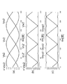
図1は、本発明の実施の形態1における交流回転機の制御装置の全体構成を示す図である。また、図2は、本発明の実施の形態1における交流回転機として用いられる3相交流発電機の構成を説明するための図である。図1に示した交流回転機1aは、図2のように、中性点N1で接続された第1の3相巻線U1、V1、W1、および中性点N2で接続された第2の3相巻線U2、V2、W2が、電気的に接続されることなく回転機の固定子に納められている3相交流回転機である。
Vu1’=Vu1+Voffset1 (1)
Vv1’=Vv1+Voffset1 (2)
Vw1’=Vw1+Voffset1 (3)
Vu2’=Vu2+Voffset2 (4)
Vv2’=Vv2+Voffset2 (5)
Vw2’=Vw2+Voffset2 (6)
Voffset1=-0.5(Vmin1+Vmax1) (7)
Dsxp1=0.5+Vx1’/Vdc1
より求める。ただし、x=U、V、Wである。例えば、Dsup1が0.6のとき、第1の電圧印加器3aは、スイッチング周期TswにおいてSup1のオン割合0.6とする。
Dsup1+Dsun1=1 (8)
Dsvp1+Dsvn1=1 (9)
Dswp1+Dswn1=1 (10)
Voffset2=-0.5(Vmin2+Vmax2) (11)
Dsxp2=0.5+Vx2’/Vdc2
より求める。ただし、x=U、V、Wである。例えば、Dsup1が0.6のとき、第1の電圧印加器3aは、スイッチング周期TswにおいてSup1のオン割合0.6とする。
Dsup2+Dsun2=1 (12)
Dsvp2+Dsvn2=1 (13)
Dswp2+Dswn2=1 (14)
Emax1=Vu1’ (15)
Emid1=Vv1’ (16)
Emin1=Vw1’ (17)
Emax2=Vu2’ (18)
Emid2=Vv2’ (19)
Emin2=Vw2’ (20)
Vs3=0.4Vdc1
Vs4=-0.4Vdc1
に設定する。
本実施の形態2における交流回転機の制御装置は、第1の検出可否判定器12cにおける演算処理が、先の実施の形態1における第1の検出可否判定器12aと異なっている。そこで、本実施の形態2における第1の検出可否判定器12cの演算処理を中心に、以下に説明する。
本実施の形態3における交流回転機の制御装置は、第1の検出可否判定器12dにおける演算処理が、先の実施の形態1における第1の検出可否判定器12aと異なっている。そこで、本実施の形態3における第1の検出可否判定器12dの演算処理を中心に、以下に説明する。

図29は、本発明の実施の形態4における交流発電機の制御装置の全体構成を示す図である。本実施の形態4の構成は、先の実施の形態1の構成と比較すると、制御部5aの代わりに、制御部5bを用いている点が異なっている。そこで、制御部5bについて、制御部5aからの変更点を中心に、以下に説明する。
加算器801bは、回転二軸上の電流Iq1’と回転二軸上の電流Iq2’との加算値(Iq1’+Iq2’)を出力する。
減算器802bは、回転二軸上の電流Iq1’を回転二軸上の電流Iq2’で減算した値(Iq1’-Iq2’)を出力する。
乗算器803bは、加算器801bから出力された加算値(Iq1’+Iq2’)をK1倍し、和電流Iq_sumを出力する。ここで、K1は、0.5である。
乗算器804bは、減算器802bから出力された減算値(Iq1’-Iq2’)をK2倍し、差電流delta_Iqを出力する。ここで、K2は、0.5である。
減算器805bは、交流回転機1aのq軸電流指令Iq*と和電流Iq_sumとの偏差dIq_sumを演算する。
加算器807bは、和電圧Vq_sumと差電圧delta_Vqとを加算した値を第1の電圧指令Vq1として出力する。
減算器808aは、和電圧Vq_sumを差電圧delta_Vqで減算した値を第2の電圧指令Vq2として出力する。
Id_sum=K1×(Id1’+Id2’)
=K1×(Id1+Id2) (23)
Iq_sum=K1×(Iq1’+Iq2’)
=K1×(Iq1+Iq2) (24)
delta_Id=K2×(Id1’-Id2’)
=K2×(Id1-Id2) (25) delta_Iq=K2×(Iq1’-Iq2’)
=K2×(Iq1-Iq2) (26)
Id_sum=K1×(Id1’+Id2’)
=K1×(2×Id2) (27)
Iq_sum=K1×(Iq1’+Iq2’)
=K1×(2×Iq2) (28)
delta_Id=K2×(Id1’-Id2’)=0 (29)
delta_Iq=K2×(Iq1’-Iq2’)=0 (30)
Id_sum=K1×(Id1’+Id2’)
=K1×(2×Id1) (31)
Iq_sum=K1×(Iq1’+Iq2’)
=K1×(2×Iq1) (32)
delta_Id=K2×(Id1’-Id2’)=0 (33)
delta_Iq=K2×(Iq1’-Iq2’)=0 (34)

Claims (19)
- 位相差を有する第1の3相巻線と第2の3相巻線とを含む交流回転機と、
直流電圧を出力する直流電源と、
前記交流回転機の電流指令と電流検出値に基づいて、第1の電圧指令と第2の電圧指令を演算する制御部と、
前記第1の電圧指令に基づいて前記直流電源から供給される直流電圧をオンオフ制御することで、前記第1の3相巻線の各相に第1の所定値以上のオン間隔またはオフ間隔で電圧を印加する第1の電圧印加器と、
前記第2の電圧指令に基づいて前記直流電源から供給される直流電圧をオンオフ制御することで、前記第2の3相巻線の各相に前記第1の所定値以上のオン間隔またはオフ間隔で電圧を印加する第2の電圧印加器と、
前記直流電源と前記第1の電圧印加器との間を流れる第1の母線電流に基づいて、第1の3相電流を検出する第1の電流検出器と、
前記直流電源と前記第2の電圧印加器との間を流れる第2の母線電流に基づいて、第2の3相電流を検出する第2の電流検出器と、
前記第1の電圧指令と前記第2の電圧指令の少なくとも1つに基づいて、前記第1の3相電流の検出可否を判定する第1の検出可否判定器と、
前記第1の電圧指令と前記第2の電圧指令の少なくとも1つに基づいて、前記第2の3相電流の検出可否を判定する第2の検出可否判定器と
を有し、
前記制御部は、
前記第1の検出可否判定器が前記第1の3相電流を検出不可能と判断した場合には、前記第1の3相巻線に印加する電圧のうちの少なくとも2相に関するオンタイミングまたはオフタイミングが、前記第1の所定値より小さい第2の所定値以内になるように、前記第1の電圧指令を生成し、
前記第2の検出可否判定器が前記第2の3相電流を検出不可能と判断した場合には、前記第2の3相巻線に印加する電圧のうちの少なくとも2相に関するオンタイミングまたはオフタイミングが、前記第2の所定値以内になるように、前記第2の電圧指令を生成する
交流回転機の制御装置。 - 前記第1の検出可否判定器は、前記第1の電圧指令を構成する3相の電圧を、大きい順に第1最大相電圧、第1中間相電圧、第1最小相電圧とした場合に、前記第1中間相電圧に基づいて、前記第1の3相電流の検出可否を判定する
請求項1に記載の交流回転機の制御装置。 - 前記第1の検出可否判定器は、前記第1中間相電圧が第3の所定値を超えた場合に、前記第1の3相電流が検出不可である第1状態と判定し、
前記制御部は、前記第1の検出可否判定器により前記第1状態と判定された場合には、前記第1最大相電圧に対応する相と前記第1中間相電圧に対応する相のオンタイミングまたはオフタイミングが、前記第2の所定値以内になるように前記第1の電圧指令を生成する
請求項2に記載の交流回転機の制御装置。 - 前記第1の検出可否判定器は、前記第1中間相電圧が第4の所定値未満の場合に、前記第1の3相電流が検出不可である第2状態と判定し、
前記制御部は、前記第1の検出可否判定器により前記第2状態と判定された場合には、前記第1中間相電圧に対応する相と前記第1最小相電圧に対応する相のオンタイミングまたはオフタイミングが、前記第2の所定値以内になるように前記第1の電圧指令を生成する
請求項2または3に記載の交流回転機の制御装置。 - 前記第1の検出可否判定器は、前記第1最大相電圧と前記第1中間相電圧との差が第5の所定値未満となった場合に、前記第1の3相電流が検出不可である第3状態と判定し、
前記制御部は、前記第1の検出可否判定器により前記第3状態と判定された場合には、前記第1最大相電圧に対応する相と前記第1中間相電圧に対応する相のオンタイミングまたはオフタイミングが、前記第2の所定値以内になるように前記第1の電圧指令を生成する
請求項2に記載の交流回転機の制御装置。 - 前記第1の検出可否判定器は、前記第1中間相電圧と前記第1最小相電圧との差が第5の所定値未満となった場合に、前記第1の3相電流が検出不可である第4状態と判定し、
前記制御部は、前記第1の検出可否判定器により前記第4状態と判定された場合には、前記第1中間相電圧に対応する相と前記第1最小相電圧に対応する相のオンタイミングまたはオフタイミングが、前記第2の所定値以内になるように前記第1の電圧指令を生成する
請求項2または5に記載の交流回転機の制御装置。 - 前記第1の検出可否判定器は、前記第1の電圧指令の電圧位相角または前記第2の電圧指令の電圧位相角に応じて、前記第1の3相電流の検出可否を判定する
ことを特徴とする請求項1または2に記載の交流回転機の制御装置。 - 前記第2の検出可否判定器は、前記第2の電圧指令を構成する3相の電圧を、大きい順に第2最大相電圧、第2中間相電圧、第2最小相電圧とした場合に、前記第2中間相電圧に基づいて、前記第2の3相電流の検出可否を判定する
請求項1から7のいずれか1項に記載の交流回転機の制御装置。 - 前記第2の検出可否判定器は、前記第2中間相電圧が第3の所定値を超えた場合に、前記第2の3相電流が検出不可である第5状態と判定し、
前記制御部は、前記第2の検出可否判定器により前記第5状態と判定された場合には、前記第2最大相電圧に対応する相と前記第2中間相電圧に対応する相のオンタイミングまたはオフタイミングが、前記第2の所定値以内になるように前記第2の電圧指令を生成する
請求項8に記載の交流回転機の制御装置。 - 前記第2の検出可否判定器は、前記第2中間相電圧が第4の所定値未満の場合に、前記第2の3相電流が検出不可である第6状態と判定し、
前記制御部は、前記第2の検出可否判定器により前記第6状態と判定された場合には、前記第2中間相電圧に対応する相と前記第2最小相電圧に対応する相のオンタイミングまたはオフタイミングが、第2の所定値以下以内になるように前記第2の電圧指令を生成する
請求項8または9に記載の交流回転機の制御装置。 - 前記第2の検出可否判定器は、前記第2最大相電圧と前記第2中間相電圧との差が第5の所定値未満となった場合に、前記第2の3相電流が検出不可である第7状態と判定し、
前記制御部は、前記第2の検出可否判定器により前記第7状態と判定された場合には、前記第2最大相電圧に対応する相と前記第2中間相電圧に対応する相のオンタイミングまたはオフタイミングが、前記第2の所定値以内になるように前記第2の電圧指令を生成する
請求項8に記載の交流回転機の制御装置。 - 前記第2の検出可否判定器は、前記第2中間相電圧と前記第2最小相電圧との差が第5の所定値未満となった場合に、前記第2の3相電流が検出不可である第8状態と判定し、
前記制御部は、前記第2の検出可否判定器により前記第8状態と判定された場合には、前記第2中間相電圧に対応する相と前記第2最小相電圧に対応する相のオンタイミングまたはオフタイミングが、前記第2の所定値以内になるように前記第2の電圧指令を生成する
請求項8または11に記載の交流回転機の制御装置。 - 前記第2の検出可否判定器は、前記第1の電圧指令の電圧位相角または前記第2の電圧指令の電圧位相角に応じて、前記第2の3相電流の検出可否を判定する
請求項8から12のいずれか1項に記載の交流回転機の制御装置。 - 前記制御部は、
前記第1の検出可否判定器が前記第1の3相電流を検出可と判定し、前記第2の検出可否判定器が前記第2の3相電流を検出可と判定した場合には、前記第1の3相電流に基づいて前記第1の電圧指令を演算するとともに、前記第2の3相電流に基づいて前記第2の電圧指令を演算し、
前記第1の検出可否判定器が前記第1の3相電流を検出不可と判定し、前記第2の検出可否判定器が前記第2の3相電流を検出可と判定した場合には、前記第2の3相電流に基づいて前記第1の電圧指令および前記第2の電圧指令を演算し、
前記第1の検出可否判定器が前記第1の3相電流を検出可と判定し、前記第2の検出可否判定器が前記第2の3相電流を検出不可と判定した場合には、前記第1の3相電流に基づいて前記第1の電圧指令および前記第2の電圧指令を演算する
請求項1から13のいずれか1項に記載の交流回転機の制御装置。 - 前記制御部は、
前記第1の検出可否判定器が前記第1の3相電流を検出可能と判定し、かつ前記第2の検出可否判定器が前記第2の3相巻線の電流を検出可能と判定した第1の場合には、前記第1の3相電流と前記第2の3相電流との和である和電流と、前記電流指令と、和電流ゲインに基づいて、和電圧を演算し、かつ前記第1の3相電流と前記第2の3相電流との差である差電流と、差電流ゲインに基づいて、差電圧を演算し、
前記第1の検出可否判定器が前記第1の3相電流を検出不可能と判定した第2の場合には、前記第2の3相電流と前記電流指令と前記和電流ゲインに基づいて、前記和電圧を演算し、かつ前記差電流または前記差電圧を零に設定し、
前記第2の検出可否判定器が前記第2の3相電流を検出不可能と判定した第3の場合には、前記第1の3相電流と前記電流指令と前記和電流ゲインに基づいて、前記和電圧を演算し、かつ前記差電流または前記差電圧を零に設定し、
前記第1の場合、前記第2の場合、および前記第3の場合のそれぞれにおいて、前記和電圧と前記差電圧に基づいて前記第1の電圧指令と前記第2の電圧指令を演算する
請求項1から14のいずれか1項に記載の交流回転機の制御装置。 - 前記制御部は、前記第1の電圧指令、前記第2の電圧指令、前記和電圧、前記交流回転機の回転速度の少なくとも1つに応じて、前記差電流ゲインを変更する
請求項15に記載の交流回転機の制御装置。 - 前記制御部は、前記第1の電圧指令、前記第2の電圧指令、前記和電圧、前記交流回転機の回転速度の少なくとも1つに応じて、前記和電流ゲインを変更する
請求項15または16に記載の交流回転機の制御装置。 - 前記位相差は、30±60×n(n:整数)である
請求項1から17のいずれか1項に記載の交流回転機の制御装置。 - 請求項1から18のいずれか1項に記載の交流回転機の制御装置を備え、
前記制御部は、ステアリング系の操舵トルクを補助するトルクを、前記交流回転機が発生するように、前記第1の電圧指令および第2の電圧指令を演算する
電動パワーステアリングの制御装置。
Priority Applications (5)
| Application Number | Priority Date | Filing Date | Title |
|---|---|---|---|
| EP15878742.4A EP3249804B1 (en) | 2015-01-21 | 2015-01-21 | Control device for ac rotary machine and control device for electric power steering |
| CN201580073466.7A CN107112938B (zh) | 2015-01-21 | 2015-01-21 | 交流旋转电机的控制装置及电动助力转向的控制装置 |
| JP2016570393A JP6227173B2 (ja) | 2015-01-21 | 2015-01-21 | 交流回転機の制御装置および電動パワーステアリングの制御装置 |
| US15/524,531 US9923504B2 (en) | 2015-01-21 | 2015-01-21 | Control device for AC rotary machine and control device for electric power steering |
| PCT/JP2015/051502 WO2016117047A1 (ja) | 2015-01-21 | 2015-01-21 | 交流回転機の制御装置および電動パワーステアリングの制御装置 |
Applications Claiming Priority (1)
| Application Number | Priority Date | Filing Date | Title |
|---|---|---|---|
| PCT/JP2015/051502 WO2016117047A1 (ja) | 2015-01-21 | 2015-01-21 | 交流回転機の制御装置および電動パワーステアリングの制御装置 |
Publications (1)
| Publication Number | Publication Date |
|---|---|
| WO2016117047A1 true WO2016117047A1 (ja) | 2016-07-28 |
Family
ID=56416613
Family Applications (1)
| Application Number | Title | Priority Date | Filing Date |
|---|---|---|---|
| PCT/JP2015/051502 WO2016117047A1 (ja) | 2015-01-21 | 2015-01-21 | 交流回転機の制御装置および電動パワーステアリングの制御装置 |
Country Status (5)
| Country | Link |
|---|---|
| US (1) | US9923504B2 (ja) |
| EP (1) | EP3249804B1 (ja) |
| JP (1) | JP6227173B2 (ja) |
| CN (1) | CN107112938B (ja) |
| WO (1) | WO2016117047A1 (ja) |
Cited By (2)
| Publication number | Priority date | Publication date | Assignee | Title |
|---|---|---|---|---|
| JP2019080427A (ja) * | 2017-10-24 | 2019-05-23 | 株式会社デンソー | 回転電機の制御装置 |
| JP2019170044A (ja) * | 2018-03-22 | 2019-10-03 | トヨタ自動車株式会社 | システム |
Families Citing this family (5)
| Publication number | Priority date | Publication date | Assignee | Title |
|---|---|---|---|---|
| BR112018076680A2 (pt) * | 2016-07-20 | 2019-04-02 | Nsk Ltd. | dispositivo de direção elétrica |
| WO2018016559A1 (ja) * | 2016-07-20 | 2018-01-25 | 日本精工株式会社 | 電動パワーステアリング装置 |
| DE102017213069A1 (de) * | 2017-07-28 | 2019-01-31 | Robert Bosch Gmbh | Verfahren zur Bestimmung einer Rotorlage einer elektrischen, rotierenden Maschine sowie eine elektrische, rotierende Maschine zur Durchführung eines solchen Verfahrens |
| US10696175B2 (en) | 2017-08-16 | 2020-06-30 | Ford Global Technologies, Llc | Variable inverter output |
| WO2019038815A1 (ja) * | 2017-08-21 | 2019-02-28 | 三菱電機株式会社 | 電力変換装置および電動パワーステアリング装置 |
Citations (5)
| Publication number | Priority date | Publication date | Assignee | Title |
|---|---|---|---|---|
| JP2003189670A (ja) * | 2001-12-14 | 2003-07-04 | Matsushita Electric Ind Co Ltd | 電動機駆動装置及びそれを用いた冷凍装置 |
| JP2008113494A (ja) * | 2006-10-30 | 2008-05-15 | Mitsubishi Electric Corp | 3相pwm信号発生装置および3相電圧型インバータ装置 |
| JP2008219956A (ja) * | 2007-02-28 | 2008-09-18 | Mitsubishi Electric Corp | 電動機駆動制御装置及び電動機 |
| JP2012178927A (ja) * | 2011-02-25 | 2012-09-13 | Sanyo Electric Co Ltd | インバータ制御装置 |
| JP2014168332A (ja) * | 2013-02-28 | 2014-09-11 | Hitachi Automotive Systems Ltd | モータ装置およびモータ駆動装置 |
Family Cites Families (9)
| Publication number | Priority date | Publication date | Assignee | Title |
|---|---|---|---|---|
| JPH03230767A (ja) | 1990-02-01 | 1991-10-14 | Toshiba Corp | 三相pwmインバータ装置における相電流検出装置 |
| JP4978429B2 (ja) * | 2007-11-01 | 2012-07-18 | アイシン・エィ・ダブリュ株式会社 | 電動機制御装置,電気自動車およびハイブリッド電気自動車 |
| JP5252229B2 (ja) * | 2009-10-02 | 2013-07-31 | アイシン・エィ・ダブリュ株式会社 | 電動機駆動装置の制御装置 |
| JP5471259B2 (ja) * | 2009-10-02 | 2014-04-16 | アイシン・エィ・ダブリュ株式会社 | 制御装置 |
| JP5402948B2 (ja) * | 2011-01-05 | 2014-01-29 | 日本精工株式会社 | モータ制御装置及びそれを用いた電動パワーステアリング装置 |
| JP5465269B2 (ja) * | 2012-03-29 | 2014-04-09 | 三菱電機株式会社 | 故障検出回路を備えた電動機駆動装置および電動機駆動装置の故障検出方法 |
| JP5556845B2 (ja) * | 2012-04-26 | 2014-07-23 | 株式会社デンソー | 3相回転機の制御装置 |
| JP5590076B2 (ja) * | 2012-07-04 | 2014-09-17 | 株式会社デンソー | 多相回転機の制御装置 |
| CN105981293B (zh) * | 2013-11-11 | 2019-06-14 | 三菱电机株式会社 | 功率转换装置 |
-
2015
- 2015-01-21 CN CN201580073466.7A patent/CN107112938B/zh active Active
- 2015-01-21 US US15/524,531 patent/US9923504B2/en active Active
- 2015-01-21 WO PCT/JP2015/051502 patent/WO2016117047A1/ja active Application Filing
- 2015-01-21 JP JP2016570393A patent/JP6227173B2/ja active Active
- 2015-01-21 EP EP15878742.4A patent/EP3249804B1/en active Active
Patent Citations (5)
| Publication number | Priority date | Publication date | Assignee | Title |
|---|---|---|---|---|
| JP2003189670A (ja) * | 2001-12-14 | 2003-07-04 | Matsushita Electric Ind Co Ltd | 電動機駆動装置及びそれを用いた冷凍装置 |
| JP2008113494A (ja) * | 2006-10-30 | 2008-05-15 | Mitsubishi Electric Corp | 3相pwm信号発生装置および3相電圧型インバータ装置 |
| JP2008219956A (ja) * | 2007-02-28 | 2008-09-18 | Mitsubishi Electric Corp | 電動機駆動制御装置及び電動機 |
| JP2012178927A (ja) * | 2011-02-25 | 2012-09-13 | Sanyo Electric Co Ltd | インバータ制御装置 |
| JP2014168332A (ja) * | 2013-02-28 | 2014-09-11 | Hitachi Automotive Systems Ltd | モータ装置およびモータ駆動装置 |
Cited By (4)
| Publication number | Priority date | Publication date | Assignee | Title |
|---|---|---|---|---|
| JP2019080427A (ja) * | 2017-10-24 | 2019-05-23 | 株式会社デンソー | 回転電機の制御装置 |
| CN111264027A (zh) * | 2017-10-24 | 2020-06-09 | 株式会社电装 | 旋转电机的控制装置 |
| CN111264027B (zh) * | 2017-10-24 | 2023-09-15 | 株式会社电装 | 旋转电机的控制装置 |
| JP2019170044A (ja) * | 2018-03-22 | 2019-10-03 | トヨタ自動車株式会社 | システム |
Also Published As
| Publication number | Publication date |
|---|---|
| US20170331405A1 (en) | 2017-11-16 |
| CN107112938B (zh) | 2019-06-21 |
| US9923504B2 (en) | 2018-03-20 |
| EP3249804B1 (en) | 2021-08-04 |
| JPWO2016117047A1 (ja) | 2017-04-27 |
| EP3249804A4 (en) | 2018-08-29 |
| JP6227173B2 (ja) | 2017-11-08 |
| EP3249804A1 (en) | 2017-11-29 |
| CN107112938A (zh) | 2017-08-29 |
Similar Documents
| Publication | Publication Date | Title |
|---|---|---|
| JP6165315B2 (ja) | 交流回転機の制御装置および電動パワーステアリングの制御装置 | |
| JP6227173B2 (ja) | 交流回転機の制御装置および電動パワーステアリングの制御装置 | |
| JP4988329B2 (ja) | 永久磁石モータのビートレス制御装置 | |
| JP6735827B2 (ja) | 電力変換装置 | |
| JPWO2008139518A1 (ja) | 電力変換装置 | |
| JP6230731B2 (ja) | 交流回転機の制御装置および電動パワーステアリングの制御装置 | |
| JPWO2015068300A1 (ja) | 電力変換装置 | |
| WO2016132427A1 (ja) | 電力変換装置 | |
| JPWO2019008676A1 (ja) | インバータ装置、及び、電動パワーステアリング装置 | |
| JP6369517B2 (ja) | 電力変換器の制御装置 | |
| JP5888074B2 (ja) | 電力変換装置 | |
| JP2011250630A (ja) | 誘導電動機の制御装置及び制御方法 | |
| JP2013066304A (ja) | 電力変換装置 | |
| JP2011217575A (ja) | 電力変換装置 | |
| JP4120868B2 (ja) | 交流電動機の制御装置 | |
| JP2005110335A (ja) | 電力変換装置 | |
| JP7251336B2 (ja) | モータ制御装置 | |
| JP5399955B2 (ja) | 電力変換装置および電力変換装置の制御方法 | |
| JP6939693B2 (ja) | パルスパターン生成装置 | |
| JP6729249B2 (ja) | 電力変換器の制御装置 | |
| JP5194886B2 (ja) | 同期電動機の可変速駆動装置 | |
| JP2002233159A (ja) | Pwm電力変換器の制御装置 | |
| JP2006211781A (ja) | 交流電動機のベクトル制御装置とその制御方法 |
Legal Events
| Date | Code | Title | Description |
|---|---|---|---|
| 121 | Ep: the epo has been informed by wipo that ep was designated in this application |
Ref document number: 15878742 Country of ref document: EP Kind code of ref document: A1 |
|
| ENP | Entry into the national phase |
Ref document number: 2016570393 Country of ref document: JP Kind code of ref document: A |
|
| WWE | Wipo information: entry into national phase |
Ref document number: 15524531 Country of ref document: US |
|
| REEP | Request for entry into the european phase |
Ref document number: 2015878742 Country of ref document: EP |
|
| NENP | Non-entry into the national phase |
Ref country code: DE |