WO2016072074A1 - 半導体装置 - Google Patents
半導体装置 Download PDFInfo
- Publication number
- WO2016072074A1 WO2016072074A1 PCT/JP2015/005450 JP2015005450W WO2016072074A1 WO 2016072074 A1 WO2016072074 A1 WO 2016072074A1 JP 2015005450 W JP2015005450 W JP 2015005450W WO 2016072074 A1 WO2016072074 A1 WO 2016072074A1
- Authority
- WO
- WIPO (PCT)
- Prior art keywords
- gate
- gate electrode
- layer
- electrode
- voltage
- Prior art date
- Legal status (The legal status is an assumption and is not a legal conclusion. Google has not performed a legal analysis and makes no representation as to the accuracy of the status listed.)
- Ceased
Links
Images







Classifications
-
- H—ELECTRICITY
- H10—SEMICONDUCTOR DEVICES; ELECTRIC SOLID-STATE DEVICES NOT OTHERWISE PROVIDED FOR
- H10D—INORGANIC ELECTRIC SEMICONDUCTOR DEVICES
- H10D12/00—Bipolar devices controlled by the field effect, e.g. insulated-gate bipolar transistors [IGBT]
-
- H—ELECTRICITY
- H10—SEMICONDUCTOR DEVICES; ELECTRIC SOLID-STATE DEVICES NOT OTHERWISE PROVIDED FOR
- H10D—INORGANIC ELECTRIC SEMICONDUCTOR DEVICES
- H10D30/00—Field-effect transistors [FET]
- H10D30/60—Insulated-gate field-effect transistors [IGFET]
-
- H—ELECTRICITY
- H10—SEMICONDUCTOR DEVICES; ELECTRIC SOLID-STATE DEVICES NOT OTHERWISE PROVIDED FOR
- H10D—INORGANIC ELECTRIC SEMICONDUCTOR DEVICES
- H10D64/00—Electrodes of devices having potential barriers
- H10D64/20—Electrodes characterised by their shapes, relative sizes or dispositions
- H10D64/27—Electrodes not carrying the current to be rectified, amplified, oscillated or switched, e.g. gates
-
- H—ELECTRICITY
- H10—SEMICONDUCTOR DEVICES; ELECTRIC SOLID-STATE DEVICES NOT OTHERWISE PROVIDED FOR
- H10D—INORGANIC ELECTRIC SEMICONDUCTOR DEVICES
- H10D64/00—Electrodes of devices having potential barriers
- H10D64/60—Electrodes characterised by their materials
- H10D64/66—Electrodes having a conductor capacitively coupled to a semiconductor by an insulator, e.g. MIS electrodes
-
- H—ELECTRICITY
- H10—SEMICONDUCTOR DEVICES; ELECTRIC SOLID-STATE DEVICES NOT OTHERWISE PROVIDED FOR
- H10D—INORGANIC ELECTRIC SEMICONDUCTOR DEVICES
- H10D84/00—Integrated devices formed in or on semiconductor substrates that comprise only semiconducting layers, e.g. on Si wafers or on GaAs-on-Si wafers
Definitions
- the present disclosure relates to a semiconductor device in which a semiconductor switching element having an insulated gate structure and a free wheel diode element (hereinafter referred to as an FWD element) are formed on a common semiconductor substrate.
- a semiconductor switching element having an insulated gate structure and a free wheel diode element hereinafter referred to as an FWD element
- Patent Document 1 a semiconductor device in which a semiconductor switching element having an insulated gate structure and an FWD element are formed on a common semiconductor substrate has been proposed (for example, Patent Document 1). reference).
- a p-type base layer is formed on the front surface side of the semiconductor substrate constituting the n ⁇ -type drift layer, and an n + -type drain layer is formed on the back surface side of the semiconductor substrate.
- a plurality of trenches reaching the drift layer through the base layer are formed, and a gate electrode is embedded in the trench through a gate insulating film.
- An n + -type source region is formed in the surface layer portion of the base layer so as to be in contact with the trench.
- a first electrode electrically connected to the base layer and the source region is formed on the front surface side of the semiconductor substrate, and a second electrode electrically connected to the drain layer is formed on the back surface side of the semiconductor substrate.
- the semiconductor switching element MOSFET element
- an FWD element having a PN junction is formed on the semiconductor substrate by the n-type drift layer and drain layer and the p-type base layer.
- a high level voltage higher than the threshold voltage of the gate insulating structure is applied to the gate electrode.
- an inversion layer connecting the source region and the drift layer is formed, and current flows between the first and second electrodes through the inversion layer.
- a low level voltage such as 0 V is applied to the gate electrode.
- a positive voltage is applied to the first electrode and a negative voltage is applied to the second electrode.
- the gate electrode has a voltage lower than the threshold voltage of the gate insulating structure and does not connect the source region and the drift layer in the vicinity of the gate electrode. Is applied to reduce the excess carriers in the FWD element. In this state, a recovery operation is performed by applying a negative voltage to the first electrode and a reverse voltage to apply a positive voltage to the second electrode, but the excess carriers in the drift layer are reduced in advance. Therefore, recovery loss can be reduced.
- a semiconductor device in the first aspect of the present disclosure, includes a first conductivity type drift layer, a second conductivity type base layer formed on the drift layer, and a surface layer portion of the base layer, A first conductivity type first impurity region which is formed apart from the drift layer with a base layer interposed therebetween and has a higher impurity concentration than the drift layer, and is sandwiched between the first impurity region and the drift layer.
- a gate insulating film disposed on the surface of the base layer, a plurality of gate electrodes disposed on the gate insulating film, and in contact with the drift layer and spaced apart from the base layer;
- An inversion layer that connects the first impurity region and the drift layer to a portion of the base layer that is located on the opposite side of the plurality of gate electrodes with the gate insulating film interposed therebetween.
- a free wheel diode element is provided between the first electrode and the second electrode.
- the plurality of gate electrodes include a first gate electrode and a second gate electrode to which independent voltages are applied.
- the threshold voltage of the insulated gate structure for forming the inversion layer connecting the first impurity region and the drift layer is the threshold voltage of the insulated gate structure having the first gate electrode and the insulation having the second gate electrode. It differs from the threshold voltage of the gate structure.
- a portion of the base layer that is in contact with the gate insulating film where the first gate electrode is disposed is included in the first impurity.
- An inversion layer that connects the region and the drift layer is formed, and the first impurity region is formed from the drift layer side to a portion of the base layer that is in contact with the gate insulating film where the second gate electrode is disposed.
- a portion of the base layer in contact with the gate insulating film where the first gate electrode and the second gate electrode are disposed is set to the first voltage as the gate voltage at which the inversion layer is formed up to a middle position toward A gate voltage at which the inversion layer is not formed is a second voltage.
- the first voltage is applied to the first gate electrode and one of the first and second voltages is applied to the second gate electrode.
- the second voltage is applied to the first gate electrode and the first voltage is applied to the second gate electrode. Is applied.
- the threshold voltage of the insulated gate structure having a part of the gate electrode and the threshold voltage of the insulated gate structure having the remaining gate electrode are made different from each other, and the FWD element is in a diode operation state.
- a first voltage that is the same as the first gate voltage applied to a part of the gate electrodes when a current is passed through the semiconductor switching element is applied to the remaining gate electrodes. Therefore, when the current is cut off from the state where the FWD element is operating as a diode, the first impurity region and the drift layer are not connected to the portion of the base layer that contacts the gate insulating film where the remaining gate electrode is disposed. Since the inversion layer is formed, recovery loss can be reduced.
- a voltage different from the first and second voltages is not required to reduce the recovery loss. That is, the recovery loss can be reduced while controlling the operation of the semiconductor switching element and the FWD element with only two kinds of gate voltages. Therefore, it is possible to suppress the configuration of the driver circuit that generates the gate voltage from becoming complicated.
- a semiconductor device in the first aspect of the present disclosure, includes a first conductivity type drift layer, a second conductivity type base layer formed on the drift layer, and a surface layer portion of the base layer, A first impurity region of a first conductivity type, which is formed apart from the drift layer with a base layer interposed therebetween and has a higher impurity concentration than the drift layer, and drifts through the first impurity region and the base layer.
- An inversion layer that connects between the first impurity region and the drift layer is formed in a portion that is opposite to each of the first gate electrode and the second gate electrode, and the first electrode and the first electrode are interposed through the inversion layer.
- a freewheeling diode element is provided. Voltages independent of each other are applied to the first gate electrode and the second gate electrode.
- the threshold voltage of the insulated gate structure for forming the inversion layer connecting the first impurity region and the drift layer is the threshold voltage of the insulated gate structure having the first gate electrode and the insulated gate structure having the second gate electrode. The threshold voltage is different.
- the first impurity region and the portion of the base layer in contact with the gate insulating film where the first gate electrode is disposed An inversion layer that connects to the drift layer is formed, and a portion of the base layer that is in contact with the gate insulating film where the second gate electrode is disposed is located on the way from the drift layer side to the first impurity region
- the inversion layer is formed at a portion of the base layer that is in contact with the gate insulating film where the first gate electrode and the second gate electrode are disposed, wherein the gate voltage at which the inversion layer is formed is a first voltage.
- the gate voltage that is not used is the second voltage.
- the first voltage is applied to the first gate electrode and one of the first and second voltages is applied to the second gate electrode.
- the second voltage is applied to the first gate electrode and the first voltage is applied to the second gate electrode. Is done.
- the threshold voltage of the insulated gate structure having a part of the gate electrode and the threshold voltage of the insulated gate structure having the remaining gate electrode are made different from each other, and the FWD element is in a diode operation state.
- a first voltage that is the same as the first gate voltage applied to a part of the gate electrodes when a current is passed through the semiconductor switching element is applied to the remaining gate electrodes. Therefore, when the current is cut off from the state where the FWD element is operating as a diode, the first impurity region and the drift layer are not connected to the portion of the base layer that contacts the gate insulating film where the remaining gate electrode is disposed. Since the inversion layer is formed, recovery loss can be reduced.
- a voltage different from the first and second voltages is not required to reduce the recovery loss. That is, the recovery loss can be reduced while controlling the operation of the semiconductor switching element and the FWD element with only two kinds of gate voltages. Therefore, it is possible to suppress the configuration of the driver circuit that generates the gate voltage from becoming complicated.
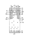
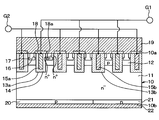
- FIG. 1 is a cross-sectional view of the semiconductor device according to the first embodiment of the present disclosure.
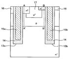
- FIG. 2 is an enlarged view of the vicinity of the first and second gate electrodes shown in FIG.
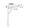
- FIG. 3 is a diagram showing the relationship between the impurity concentration along the line AA ′ in FIG. 2 and the impurity concentration along the line BB ′ in FIG.
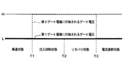
- FIG. 4 is a timing chart when the FWD element is switched from the diode operating state to the OFF state.
- FIG. 5A is a diagram showing an operating state of the FWD element in a conductive state;
- FIG. 1 is a cross-sectional view of the semiconductor device according to the first embodiment of the present disclosure.
- FIG. 2 is an enlarged view of the vicinity of the first and second gate electrodes shown in FIG.
- FIG. 3 is a diagram showing the relationship between the impurity concentration along the line AA ′ in FIG. 2 and the impurity concentration along the line BB ′ in FIG.
- FIG. 4 is
- FIG. 5B is a diagram illustrating an operation state of the FWD element in the injection suppression state
- FIG. 5C is a diagram illustrating an operation state of the FWD element in the recovery state
- FIG. 5D is a diagram showing an operating state of the FWD element in a current interrupting state
- FIG. 6 is a diagram illustrating an example of a threshold voltage in the semiconductor device illustrated in FIG.
- FIG. 7 is a diagram illustrating an example of the gate voltage applied to the second gate electrode in the injection suppression state
- FIG. 8 is a cross-sectional view of the semiconductor device according to the second embodiment of the present disclosure.
- FIG. 9A to FIG. 9D are cross-sectional views showing manufacturing steps of the semiconductor device shown in FIG. FIG. 10A to FIG.
- FIG. 11A is a cross-sectional view of a semiconductor device according to a third embodiment of the present disclosure
- FIG. 11B is a cross-sectional view different from FIG. 11A.
- a first embodiment of the present disclosure will be described with reference to the drawings.
- a semiconductor device including a reverse conducting IGBT (RC-IGBT) in which an IGBT element and an FWD element are formed on a common semiconductor substrate will be described.
- the semiconductor device of the present embodiment is preferably used for a power conversion device such as an inverter or a converter, for example.
- the semiconductor device has a semiconductor substrate 10 constituting a drift layer 11, and a p-type base layer 12 is formed on the drift layer 11 (on the one surface 10 a side of the semiconductor substrate 10). Yes.
- a plurality of trenches 13 a and 13 b are formed so as to penetrate the base layer 12 and reach the drift layer 11, and the base layer 12 is separated into a plurality by the trenches 13 a and 13 b.
- the trenches 13a and 13b are formed at equal intervals along one direction (the depth direction in the drawing in FIG. 2) of the surface directions of the one surface 10a of the semiconductor substrate 10. Further, one surface 10 a of the semiconductor substrate 10 is configured by one surface of the base layer 12 opposite to the drift layer 11.
- a gate insulating film 14 formed so as to cover the wall surfaces of the respective trenches 13a and 13b, and a gate electrode 15a formed of polysilicon or the like formed on the gate insulating film 14 , 15b.
- a trench gate structure is configured.
- the gate electrodes 15a and 15b formed in the trenches 13a and 13b have first and second gate terminals G1 and G2 in which a part of the gate electrodes 15a and the remaining gate electrode 15b are different. It is connected to the. That is, a gate voltage independent from each other is applied to some of the gate electrodes 15a and the remaining gate electrodes 15b.
- a part of the gate electrodes is designated as the first gate electrode 15a
- the remaining gate electrode is designated as the second gate electrode 15b
- the trench 13a in which the first gate electrode 15a is disposed is designated as the first trench 13a.
- the trench 13b in which the two-gate electrode 15b is disposed will be described as a second trench 13b.
- first gate electrode 15a and the second gate electrode 15b are perpendicular to the extending direction of the first and second trenches 13a and 13b (FIG. 1). In the left and right direction of the middle paper surface).
- an n + -type emitter region 16 and a p + -type contact region 17 sandwiched between the emitter regions 16 are formed.
- the emitter region 16 is configured to have a higher impurity concentration than the drift layer 11, is terminated in the base layer 12, and is in contact with the side surfaces of the first and second trenches 13a and 13b.
- the contact region 17 has a higher impurity concentration than the base layer 12, and is formed so as to terminate in the base layer 12, similarly to the emitter region 16.
- the emitter region 16 is formed on the side surfaces of the first and second trenches 13a and 13b along the longitudinal direction of the first and second trenches 13a and 13b in the region between the first and second trenches 13a and 13b. It extends in the shape of a rod so as to be in contact with the first and second trenches 13a and 13b, and terminates inside the tip.
- the contact region 17 is sandwiched between the two emitter regions 16 and extends in a rod shape along the longitudinal direction of the first and second trenches 13a and 13b (that is, the emitter region 16). In the present embodiment, the contact region 17 is formed deeper than the emitter region 16 with respect to the one surface 10a of the semiconductor substrate 10.
- the depth of the emitter region 16 in contact with the first trench 13a is made deeper than the depth of the emitter region 16 in contact with the second trench 13b.
- current flows in the thickness direction of the semiconductor substrate 10, and therefore drifts between the emitter region 16 in the current flow direction of the base layer 12 and the drift.
- the portion between the layer 11 and the second gate electrode 15b is located on the opposite side to the first gate electrode 15a with the gate insulating film 14 in between. It is shorter than the part. That is, as shown in FIG. 3, each emitter region 16 is formed so that the peak concentration positions of the emitter region 16 in contact with the first trench 13a and the emitter region 16 in contact with the second trench 13b are different. .
- the threshold voltage Vth of the gate insulating structure having the first gate electrode 15a is different from the threshold voltage Vth of the gate insulating structure having the second gate electrode 15b. Specifically, since the emitter region 16 in contact with the second trench 13b is formed shallower than the emitter region 16 in contact with the first trench 13a, the threshold voltage Vth of the insulated gate structure having the second gate electrode 15b is It is higher than the threshold voltage Vth of the insulated gate structure having one gate electrode 15a.
- the threshold voltage Vth of the insulated gate structure in the present embodiment forms an inversion layer that connects the emitter region 16 and the drift layer 11 when a gate voltage is applied to the first and second gate electrodes 15a and 15b. This is the minimum voltage required for this purpose.
- an interlayer insulating film 18 made of BPSG or the like is formed on the base layer 12 (one surface 10a of the semiconductor substrate 10).
- a contact hole 18 a is formed in the interlayer insulating film 18 to expose a part of the emitter region 16 and the contact region 17.
- a first electrode 19 is formed on the interlayer insulating film 18.
- the first electrode 19 is electrically connected to the emitter region 16 and the contact region 17 through the contact hole 18a. That is, the first electrode 19 functions as an emitter electrode in the IGBT element and also functions as an anode element in the FWD element.
- a p-type collector layer 20 and an n-type cathode layer 21 are formed on the drift layer 11 opposite to the base layer 12 side (the other surface 10b side of the semiconductor substrate 10). That is, the IGBT element and the FWD element are basically partitioned depending on whether the layer formed on the other surface 10 b side of the semiconductor substrate 10 is the collector layer 20 or the cathode layer 21.
- a second electrode 22 is formed on the collector layer 20 and the cathode layer 21 (the other surface 10b of the semiconductor substrate 10).
- the second electrode 22 functions as a collector electrode in the IGBT element and functions as a cathode electrode in the FWD element.
- an FWD element having a PN junction with the base layer 12 and the contact region 17 as an anode and the drift layer 11 and the cathode layer 21 as a cathode is configured.
- the emitter region 16 corresponds to the first impurity region of the present disclosure
- the cathode layer 21 corresponds to the second impurity region of the present disclosure.
- the n-type, n + type, and n ⁇ type correspond to the first conductivity type of the present disclosure
- the p type and p + type correspond to the second conductivity type of the present disclosure.
- gate voltages and operations applied to the first and second gate electrodes 15a and 15b in the semiconductor device will be described.
- gate voltages independent of each other are applied to the first and second gate electrodes 15a and 15b.
- the PN junction formed between the base layer 12 and the drift layer 11 is in a reverse conduction state. Therefore, when a low level (for example, 0 V) voltage is applied to the first and second gate electrodes 15a and 15b, a depletion layer is formed in the PN junction, and the first and second electrodes 19 and 22 are connected. Current is cut off.
- a low level (for example, 0 V) voltage is applied to the first and second gate electrodes 15a and 15b, a depletion layer is formed in the PN junction, and the first and second electrodes 19 and 22 are connected. Current is cut off.
- a high level voltage is applied to the first gate electrode 15a while the first electrode 19 is grounded and a positive voltage is applied to the second electrode 22.
- a low level voltage is applied to the two gate electrodes 15b.
- an inversion layer is formed in a portion of the base layer 12 that is in contact with the first trench 13a where the first gate electrode 15a is disposed, and the first and second electrodes 19 and 22 are interposed via the inversion layer. Current flows through
- the threshold voltage Vth of the insulated gate structure having the second gate electrode 15b is set higher than the threshold voltage Vth of the insulated gate structure having the first gate electrode 15a.
- the high level voltage is equal to or higher than the threshold voltage Vth of the insulated gate structure having the first gate electrode 15a and less than the threshold voltage Vth of the insulated gate structure having the second gate electrode 15b. Is the voltage. That is, when a high level gate voltage is simultaneously applied to the first and second gate electrodes 15 a and 15 b, the inversion layer that connects the emitter region 16 and the drift layer 11 is formed in the first trench 13 a of the base layer 12. It is formed only in the part along.
- the high level voltage corresponds to the first voltage of the present disclosure
- the low level voltage corresponds to the second voltage of the present disclosure.
- the IGBT element when the IGBT element is turned off and the FWD element is diode-operated (turned on), the voltage applied to the first electrode 19 and the second electrode 22 is switched, and the positive voltage is applied to the first electrode 19. And the second electrode 22 is grounded. Then, a low level voltage is applied to the first and second gate electrodes 15a and 15b. As a result, the inversion layer is not formed in the portion of the base layer 12 in contact with the first trench 13a, and the FWD element performs a diode operation.
- the FWD element When the current is cut off and turned off after the FWD element is operated as a diode, as shown in FIG. 4, the FWD element is in a conduction state (on state), an injection suppression state, a recovery state, a current.
- the state changes in the order of the cutoff state (off state).
- the high level voltage is equal to or higher than the threshold voltage Vth of the insulated gate structure having the first gate electrode 15a and the threshold voltage of the insulated gate structure having the second gate electrode 15b.
- the voltage is less than Vth. That is, an inversion layer that does not connect the emitter region 16 and the drift layer 11 is formed in a portion of the base layer 12 that is in contact with the second trench 13b.
- the inversion layer 23 is formed from the portion on the drift layer 11 side in the portion in contact with the second trench 13 b in the base layer 12 to a midway position toward the emitter region 16.
- the minority carriers in the base layer 12 are reduced, the number of holes, which are the majority carriers in the base layer 12, is reduced due to the charge neutrality condition, and the electrons accumulated in the drift layer 11 pass through the inversion layer 23.
- the first electrode 19 Through the first electrode 19.
- the semiconductor device is set so that the threshold voltage Vth of the insulated gate structure having the first gate electrode 15a is 8V and the threshold voltage Vth of the insulated gate structure having the second gate electrode 15b is 25V.
- the voltage between the first and second electrodes 19 and 22 is increased by applying a voltage of 15 V or more to the second gate electrode 15b. That is, the absolute value of the forward voltage Vf of the FWD element increases.
- the threshold voltage Vth of the insulated gate structure having the second gate electrode 15b is 25V, a short circuit occurs when a gate voltage of 25V or more is applied to the second gate electrode 15b.
- FIG. 7 shows a simulation result when the forward current when the FWD element is operating as a diode is 400 A / cm 2 .
- Such a semiconductor device for example, is used to form an ion implantation step for forming the emitter region 16 in contact with the first trench 13a and an emitter region 16 in contact with the second trench 13b in a normal semiconductor manufacturing process.
- the ion implantation process is performed as a separate process, and the acceleration voltage and the like in each ion implantation process are appropriately changed.
- gate voltages independent of each other are applied to the first and second gate electrodes 15a and 15b, and the threshold voltage Vth of the insulated gate structure having the first gate electrode 15a and the first The threshold voltage Vth of the insulated gate structure having two gate electrodes 15b is made different.
- the high level applied to the second gate electrode 15b is applied to the first gate electrode 15a when the IGBT element is turned on.
- the first and second gate electrodes 15a and 15b are alternately formed. For this reason, when operating a semiconductor device as an IGBT element and operating as a FWD element, it can control that current concentration occurs.
- the semiconductor device in which the IGBT element and the FWD element are formed on the semiconductor substrate 10 has been described.
- the collector layer 20 is not provided on the back side of the semiconductor substrate 10, and the MOSFET element and the FWD element are semiconductors.
- a semiconductor device formed on the substrate 10 may be used. Similar effects can be obtained also in such a semiconductor device.
- the gate insulating film 14 disposed in the second trench 13b is thicker than the gate insulating film 14 disposed in the first trench 13a.
- the threshold voltage Vth of the insulated gate structure having the second gate electrode 15b is increased. You may make it become higher than the threshold voltage Vth of the insulated gate structure which has the 1st gate electrode 15b.
- the threshold voltage Vth of the insulated gate structure having the second gate electrode 15b is made higher than the threshold voltage Vth of the insulated gate structure having the first gate electrode 15b.
- a semiconductor substrate 10 is prepared, and an oxide film 31 is formed on one surface 10a of the semiconductor substrate 10 by a thermal oxidation method or the like.
- anisotropic etching such as reactive ion etching (RIE) is performed using the oxide film 31 as a mask to form the first trench 13a.
- RIE reactive ion etching
- CDE chemical dry etching
- a gate insulating film 14 disposed in the first trench 13a is formed by a thermal oxidation method or the like.
- doped Poly-Si is formed on the gate insulating film 14 disposed in the first trench 13a to form the first gate electrode 15a, and the semiconductor substrate 10 is again formed.
- An oxide film 32 is formed on one surface 10a.
- the second trench 13b is formed by performing anisotropic etching such as reactive ion etching (RIE) using the oxide film 32 as a mask. Then, the process of removing the damage of the wall surface of the formed 2nd trench 13b is performed by performing chemical dry etching (CDE) etc. as needed.
- anisotropic etching such as reactive ion etching (RIE)
- CDE chemical dry etching
- the gate insulating film 14 disposed in the second trench 13b is formed by a thermal oxidation method or the like.
- the heating temperature is set higher or the heating time is made longer than the thermal oxidation method in the step of FIG.
- a gate insulating film 14 thicker than the gate insulating film 14 disposed in the trench 13a can be formed in the second trench 13b.
- doped Poly-Si is formed on the gate insulating film 14 disposed in the second trench 13b to form the second gate electrode 15b, and again the semiconductor substrate 10 An oxide film 33 is formed on one surface 10a.
- a known semiconductor manufacturing process is performed to form the base layer 12, the emitter region 16, the collector layer 20, the cathode layer 21, the first electrode 19, and the second electrode 22, so that FIG. The semiconductor device shown is manufactured.
- the present embodiment is a lateral semiconductor device in which a current flows in the plane direction of the semiconductor substrate 10 as compared to the first embodiment, and a semiconductor device in which a MOSFET element and an FWD element are formed on the semiconductor substrate 10. Since other aspects are the same as those in the first embodiment, description thereof is omitted here.
- the base layer 12 is formed in a predetermined region of the surface layer portion of the drift layer 11, and the source region 41 and the contact region are formed in the predetermined region in the base layer 12. 42 is formed.
- An n + -type drain layer 43 spaced from the base layer 12 is formed on the surface layer portion of the drift layer 11.
- the source region 41 corresponds to the first impurity region of the present disclosure
- the drain layer 43 corresponds to the second impurity region of the present disclosure.
- the first and second gate electrodes 15a and 15b are extended on the one surface 10a of the semiconductor substrate 10 via the gate insulating film 14 in the channel width direction (longitudinal direction of the base layer 12 and the like). These first and second gate electrodes 15a and 15b are connected to different first and second gate terminals G1 and G2 as in the first embodiment, so that gate voltages independent of each other are applied. Yes.
- a first electrode 19 that is electrically connected to the source region 41 and the contact region 42 is disposed on the one surface 10 a of the semiconductor substrate 10, and a second electrode that is electrically connected to the drain layer 43. 22 is arranged. 11A and 11B, the interlayer insulating film 18 formed on the one surface 10a of the semiconductor substrate 10 is omitted.
- the planar lateral MOSFET element and the FWD element are formed on the common semiconductor substrate 10 by such a structure.
- a high level voltage is applied to the first gate electrode 15a and the base layer 12 is inverted to a portion located below the first gate electrode 15a.
- a current flows between the first electrode 19 and the second electrode 22. Specifically, a current flows along the surface direction of the semiconductor substrate 10 (the left-right direction in FIG. 11A and FIG. 11B).
- the length between the source region 41 and the drift layer 11 along the current flow direction in the base layer 12 is opposite to that of the first gate electrode 15a with the gate insulating film 14 interposed therebetween.
- the portion located on the side is shorter than the portion located on the opposite side to the second gate electrode 15b with the gate insulating film 14 interposed therebetween.
- the threshold voltage Vth of the insulated gate structure having the second gate electrode 15b is higher than the threshold voltage Vth of the insulated gate structure having the first gate electrode 15a.
- the FWD element operates as a diode.
- a high-level gate voltage is applied to the second gate electrode 15b to configure the injection suppression state, thereby obtaining the same effect as in the first embodiment. it can.
- the first conductivity type is n-type and the second conductivity type is p-type.
- the first conductivity type is p-type and the second conductivity type is n-type. You can also.
- the structure for making the threshold voltage Vth of the gate insulating structure having the first gate electrode 15a different from the threshold voltage Vth of the gate insulating structure having the second gate electrode 15b can be changed as appropriate. is there.
- the gradient of the impurity concentration is made in the base layer 12, and the impurity concentration of the portion in contact with the second trench 13b in the base layer 12 is higher than the impurity concentration of the portion in contact with the first trench 13a. It may be made to become.
- the arrangement method of the first and second gate electrodes 15a and 15b can be changed as appropriate.
- the first and second trenches 13a and 13b are alternately extended in the vertical direction. It does not need to be arranged.
- two second gate electrodes 15b may be arranged between adjacent first gate electrodes 15a, or the first gate electrode 15a and the second gate electrode 15b may be arranged together. It may be. In this case, it is preferable that the second gate electrode 15 b is disposed on the cathode layer 21.
- the arrangement method of the first and second gate electrodes 15a and 15b can be changed as appropriate.
- a high level gate voltage may be applied to the second gate electrode 15b.
- the inversion layer 23 that does not connect the emitter region 16 and the drift layer 11 is formed in a portion of the base layer 12 that is in contact with the second trench 13 b, current (electrons) is passed through the inversion layer 23.
- the inversion layer 23 makes it easy to accumulate holes in the drift layer 11. For this reason, it is possible to reduce the ON voltage when the IGBT element is in the ON state.
- the first and second trenches 13a and 13b are formed in the semiconductor substrate 10, and the first and second gate electrodes 15a and 15b are arranged in the first and second trenches 13a and 13b. You may do it. That is, a horizontal semiconductor device having a trench gate structure may be used.
- the above embodiments can be appropriately combined.
- the second embodiment may be combined with the first and third embodiments, and the thickness of the gate insulating film 14 may be changed as appropriate.
Landscapes
- Electrodes Of Semiconductors (AREA)
- Insulated Gate Type Field-Effect Transistor (AREA)
- Metal-Oxide And Bipolar Metal-Oxide Semiconductor Integrated Circuits (AREA)
Abstract
半導体装置は、第1不純物領域(16、41)とドリフト層(11)間のベース層(12)上のゲート絶縁膜(14)を介した第一、第二ゲート電極(15a、15b)と、第2不純物領域(21、43)と、電極(19、22)とを有する半導体スイッチング素子を備え、前記ベース層と前記ドリフト層とによるFWD素子を備えている。前記第一ゲート電極と対向する前記ベース層に反転層が形成され、前記第二ゲート電極と対向するベース層に途中位置まで反転層が形成される第1電圧、ベース層に前記反転層が形成されない第2電圧を定義する。前記半導体スイッチング素子に電流を流す際には、前記第一ゲート電極に前記第1電圧が印加され、前記第二ゲート電極に前記第1または第2電圧が印加される。前記FWD素子の電流を遮断する際、前記第一ゲート電極に前記第2電圧が印加され、前記第二ゲート電極に前記第1電圧が印加される。
Description
本出願は、2014年11月3日に出願された日本特許出願番号2014-223866号に基づくもので、ここにその記載内容を援用する。
本開示は、絶縁ゲート構造を有する半導体スイッチング素子とフリーホイールダイオード素子(以下、FWD素子という)とが共通の半導体基板に形成された半導体装置に関するものである。
従来より、インバータやコンバータ等の電力変換装置に用いるスイッチング素子として、絶縁ゲート構造の半導体スイッチング素子とFWD素子とが共通の半導体基板に形成された半導体装置が提案されている(例えば、特許文献1参照)。
具体的には、この半導体装置では、n-型のドリフト層を構成する半導体基板の表面側にp型のベース層が形成され、半導体基板の裏面側にn+型のドレイン層が形成されている。そして、ベース層を貫通してドリフト層に達する複数のトレンチが形成され、トレンチ内には、ゲート絶縁膜を介してゲート電極が埋め込まれている。また、ベース層の表層部には、トレンチと接するようにn+型のソース領域が形成されている。さらに、半導体基板の表面側にはベース層およびソース領域と電気的に接続される第1電極が形成され、半導体基板の裏面側にはドレイン層と電気的に接続される第2電極が形成されている。以上のようにして、半導体基板に半導体スイッチング素子(MOSFET素子)が形成されている。
また、上記構成とされていることにより、半導体基板には、n型のドリフト層およびドレイン層とp型のベース層とによってPN接合を有するFWD素子が形成されている。
上記半導体装置では、半導体スイッチング素子として動作させる場合には、ゲート電極にゲート絶縁構造の閾値電圧以上のハイレベルの電圧を印加する。これにより、ソース領域とドリフト層とを繋ぐ反転層が形成され、当該反転層を介して第1、第2電極間に電流が流れる。
また、FWD素子がダイオード動作している際(FWD素子の順方向に電流が流れている際)には、ゲート電極に0V等のローレベルの電圧が印加される。なお、FWD素子が通常のダイオード動作をする際には、第1電極には正の電圧が印加されると共に第2電極に負の電圧が印加される。そして、FWD素子のダイオード動作を停止してオフ状態にする直前には、ゲート電極にゲート絶縁構造の閾値電圧未満の電圧であり、ゲート電極の近傍にソース領域とドリフト層とを繋がない反転層が形成されるミドルレベルの電圧を印加し、FWD素子内の過剰キャリアを減少させる。この状態で、第1電極に負の電圧を印加すると共に第2電極に正の電圧を印加する逆電圧印加を行うことにより、リカバリ動作が行われるが、ドリフト層内の過剰キャリアを予め少なくしているため、リカバリ損失を低減することができる。
しかしながら、上記半導体装置では、ゲート電極には、ハイレベル、ローレベル、ミドルレベルの3種類のゲート電圧が印加されるため、3種類のゲート電圧を生成するためのドライバ回路が必要になり、当該ドライバ回路が複雑になるという問題がある。
なお、上記では半導体基板の厚さ方向に電流を流す縦型の半導体装置について説明したが、このような問題は半導体基板の平面方向に電流を流す横型の半導体装置にも同様に発生する。また、半導体基板にコレクタ層およびカソード層が形成された逆導通型IGBT(RC-IGBT)においても同様に発生する。
本開示は、リカバリ損失の低減を図ることができ、かつ、ゲート電極に印加するゲート電圧を生成するためのドライバ回路の構成が複雑になることを抑制できる半導体装置を提供することを目的とする。
本開示の第一の態様において、半導体装置は、第1導電型のドリフト層と、前記ドリフト層上に形成された第2導電型のベース層と、前記ベース層の表層部であって、前記ベース層を挟んで前記ドリフト層から離間して形成され、前記ドリフト層よりも高不純物濃度とされた第1導電型の第1不純物領域と、前記第1不純物領域と前記ドリフト層の間に挟まれた前記ベース層の表面に配置されたゲート絶縁膜と、前記ゲート絶縁膜上に配置された複数のゲート電極と、前記ドリフト層と接触すると共に前記ベース層から離間して形成され、前記ドリフト層よりも高不純物濃度とされた第1導電型の第2不純物領域と、前記ベース層および前記第1不純物領域と電気的に接続される第1電極と、前記第2不純物領域と電気的に接続される第2電極と、を有し、前記ベース層のうち、前記ゲート絶縁膜を挟んで前記複数のゲート電極と反対側に位置する部分に前記第1不純物領域と前記ドリフト層との間を繋ぐ反転層を形成し、当該反転層を介して前記第1電極と前記第2電極との間に電流を流す半導体スイッチング素子を備えていると共に、前記ベース層と前記ドリフト層とによるPN接合を有し、前記第1電極と前記第2電極との間に電流を流すフリーホイールダイオード素子を備えている。前記複数のゲート電極は、互いに独立した電圧が印加される第一のゲート電極と第二のゲート電極を含む。前記第1不純物領域と前記ドリフト層とを繋ぐ反転層を形成するための絶縁ゲート構造の閾値電圧は、第一のゲート電極を有する絶縁ゲート構造の閾値電圧と、第二のゲート電極を有する絶縁ゲート構造の閾値電圧とで異なっている。前記第一のゲート電極および前記第二のゲート電極にゲート電圧が印加された際、前記ベース層のうちの前記第一のゲート電極が配置される前記ゲート絶縁膜と接する部分に前記第1不純物領域と前記ドリフト層とを繋ぐ反転層が形成されると共に、前記ベース層のうちの前記第二のゲート電極が配置される前記ゲート絶縁膜と接する部分に前記ドリフト層側から前記第1不純物領域に向かう途中位置まで反転層が形成される前記ゲート電圧を第1電圧とし、前記ベース層のうちの前記第一のゲート電極および前記第二のゲート電極が配置される前記ゲート絶縁膜と接する部分に前記反転層が形成されないゲート電圧を第2電圧とする。前記半導体スイッチング素子に電流を流す際には、前記第一のゲート電極に前記第1電圧が印加されると共に前記第二のゲート電極に前記第1、第2電圧のいずれか一方が印加される。前記フリーホイールダイオード素子の順方向に電流が流れている状態から当該電流を遮断する際、前記第一のゲート電極に前記第2電圧が印加されると共に前記第二のゲート電極に前記第1電圧が印加される。
上記の半導体装置によれば、一部のゲート電極を有する絶縁ゲート構造の閾値電圧と残部のゲート電極を有する絶縁ゲート構造の閾値電圧とが異なるようにし、FWD素子がダイオード動作している状態から電流を遮断する際、残部のゲート電極に、半導体スイッチング素子に電流を流す際に一部のゲート電極に印加する第1ゲート電圧と同じ第1電圧を印加している。このため、FWD素子がダイオード動作している状態から電流を遮断する際、ベース層のうちの残部のゲート電極が配置されるゲート絶縁膜と接する部分に第1不純物領域とドリフト層とを繋がない反転層が形成されるため、リカバリ損失の低減を図ることができる。つまり、リカバリ損失の低減を図るために、第1、第2電圧と異なる電圧を必要としない。すなわち、2種類のゲート電圧のみで半導体スイッチング素子およびFWD素子の作動を制御しつつ、リカバリ損失の低減も図ることができる。したがって、ゲート電圧を生成するドライバ回路の構成が複雑になることを抑制できる。
本開示の第一の態様において、半導体装置は、第1導電型のドリフト層と、前記ドリフト層上に形成された第2導電型のベース層と、前記ベース層の表層部であって、前記ベース層を挟んで前記ドリフト層から離間して形成され、前記ドリフト層よりも高不純物濃度とされた第1導電型の第1不純物領域と、第1不純物領域およびベース層を貫通して、ドリフト層に達する第一トレンチおよび第二トレンチと、前記第一トレンチおよび第二トレンチ内に各々配置されたゲート絶縁膜と、前記ゲート絶縁膜上に配置された第一ゲート電極および第二ゲート電極と、前記ドリフト層と接触すると共に前記ベース層から離間して形成され、前記ドリフト層よりも高不純物濃度とされた第1導電型の第2不純物領域と、前記ベース層および前記第1不純物領域と電気的に接続される第1電極と、前記第2不純物領域と電気的に接続される第2電極と、を有し、前記ベース層のうち、前記ゲート絶縁膜を挟んで前記第一ゲート電極および第二ゲート電極の各々と反対側に位置する部分に前記第1不純物領域と前記ドリフト層との間を繋ぐ反転層を形成し、当該反転層を介して前記第1電極と前記第2電極との間に電流を流す半導体スイッチング素子を備えていると共に、前記ベース層と前記ドリフト層とによるPN接合を有し、前記第1電極と前記第2電極との間に電流を流すフリーホイールダイオード素子を備えている。第一ゲート電極と第二ゲート電極は、互いに独立した電圧が印加される。前記第1不純物領域と前記ドリフト層とを繋ぐ反転層を形成するための絶縁ゲート構造の閾値電圧は、第一ゲート電極を有する絶縁ゲート構造の閾値電圧と、第二ゲート電極を有する絶縁ゲート構造の閾値電圧とで異なっている。前記第一ゲート電極および前記第二ゲート電極にゲート電圧が印加された際、前記ベース層のうちの前記第一ゲート電極が配置される前記ゲート絶縁膜と接する部分に前記第1不純物領域と前記ドリフト層とを繋ぐ反転層が形成されると共に、前記ベース層のうちの前記第二ゲート電極が配置される前記ゲート絶縁膜と接する部分に前記ドリフト層側から前記第1不純物領域に向かう途中位置まで反転層が形成される前記ゲート電圧を第1電圧とし、前記ベース層のうちの前記第一ゲート電極および前記第二ゲート電極が配置される前記ゲート絶縁膜と接する部分に前記反転層が形成されないゲート電圧を第2電圧とする。前記半導体スイッチング素子に電流を流す際には、前記第一ゲート電極に前記第1電圧が印加されると共に前記第二ゲート電極に前記第1、第2電圧のいずれか一方が印加される。前記フリーホイールダイオード素子の順方向に電流が流れている状態から当該電流を遮断する際、前記第一ゲート電極に前記第2電圧が印加されると共に前記第二ゲート電極に前記第1電圧が印加される。
上記の半導体装置によれば、一部のゲート電極を有する絶縁ゲート構造の閾値電圧と残部のゲート電極を有する絶縁ゲート構造の閾値電圧とが異なるようにし、FWD素子がダイオード動作している状態から電流を遮断する際、残部のゲート電極に、半導体スイッチング素子に電流を流す際に一部のゲート電極に印加する第1ゲート電圧と同じ第1電圧を印加している。このため、FWD素子がダイオード動作している状態から電流を遮断する際、ベース層のうちの残部のゲート電極が配置されるゲート絶縁膜と接する部分に第1不純物領域とドリフト層とを繋がない反転層が形成されるため、リカバリ損失の低減を図ることができる。つまり、リカバリ損失の低減を図るために、第1、第2電圧と異なる電圧を必要としない。すなわち、2種類のゲート電圧のみで半導体スイッチング素子およびFWD素子の作動を制御しつつ、リカバリ損失の低減も図ることができる。したがって、ゲート電圧を生成するドライバ回路の構成が複雑になることを抑制できる。
本開示についての上記目的およびその他の目的、特徴や利点は、添付の図面を参照しながら下記の詳細な記述により、より明確になる。その図面は、
図1は、本開示の第1実施形態における半導体装置の断面図であり、
図2は、図1に示す第1、第2ゲート電極近傍の拡大図であり、
図3は、図2中のA-A´線に沿った不純物濃度と、B-B´線に沿った不純物濃度との関係を示す図であり、
図4は、FWD素子がダイオード動作している状態からオフ状態に切り換える際のタイミングチャートであり、
図5Aは、導通状態におけるFWD素子の動作状態を示す図であり、
図5Bは、注入抑制状態におけるFWD素子の動作状態を示す図であり、
図5Cは、リカバリ状態におけるFWD素子の動作状態を示す図であり、
図5Dは、電流遮断状態におけるFWD素子の動作状態を示す図であり、
図6は、図1に示す半導体装置における閾値電圧の1例を示す図であり、
図7は、注入抑制状態における第2ゲート電極に印加するゲート電圧の1例を示す図であり、
図8は、本開示の第2実施形態における半導体装置の断面図であり、
図9(a)から図9(d)は、図8に示す半導体装置の製造工程を示す断面図であり、
図10(a)から図10(c)は、図9(d)に続く半導体装置の製造工程を示す断面図であり、
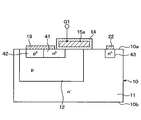
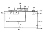
図11Aは、本開示の第3実施形態における半導体装置の断面図であり、
図11Bは、図11Aとは別断面の断面図である。
以下、本開示の実施形態について図に基づいて説明する。なお、以下の各実施形態相互において、互いに同一もしくは均等である部分には、同一符号を付して説明を行う。
(第1実施形態)
本開示の第1実施形態について図面を参照しつつ説明する。本実施形態では、IGBT素子とFWD素子とが共通の半導体基板に形成された逆導通型IGBT(RC-IGBT)を備える半導体装置について説明する。なお、本実施形態の半導体装置は、例えば、インバータやコンバータ等の電力変換装置に利用されると好適である。
本開示の第1実施形態について図面を参照しつつ説明する。本実施形態では、IGBT素子とFWD素子とが共通の半導体基板に形成された逆導通型IGBT(RC-IGBT)を備える半導体装置について説明する。なお、本実施形態の半導体装置は、例えば、インバータやコンバータ等の電力変換装置に利用されると好適である。
図1に示されるように、半導体装置は、ドリフト層11を構成する半導体基板10を有し、当該ドリフト層11上(半導体基板10の一面10a側)にp型のベース層12が形成されている。そして、ベース層12を貫通してドリフト層11に達するように複数のトレンチ13a、13bが形成され、このトレンチ13a、13bによってベース層12が複数個に分離されている。
なお、各トレンチ13a、13bは、半導体基板10の一面10aの面方向のうちの一方向(図2中紙面奥行き方向)に沿って等間隔に形成されている。また、半導体基板10の一面10aは、ベース層12のうちのドリフト層11と反対側の一面にて構成されている。
そして、各トレンチ13a、13b内は、各トレンチ13a、13bの壁面を覆うように形成されたゲート絶縁膜14と、このゲート絶縁膜14上に形成されたポリシリコン等により構成されるゲート電極15a、15bとにより埋め込まれている。これにより、トレンチゲート構造が構成されている。
ここで、本実施形態では、各トレンチ13a、13b内に形成されたゲート電極15a、15bは、一部のゲート電極15aと残部のゲート電極15bとが異なる第1、第2ゲート端子G1、G2に接続されている。つまり、一部のゲート電極15aと残部のゲート電極15bとは、互いに独立したゲート電圧が印加されるようになっている。以下では、一部のゲート電極を第1ゲート電極15aとすると共に、残部のゲート電極を第2ゲート電極15bとし、第1ゲート電極15aが配置されるトレンチ13aを第1トレンチ13aとすると共に第2ゲート電極15bが配置されるトレンチ13bを第2トレンチ13bとして説明する。なお、本実施形態では、第1ゲート電極15aおよび第2ゲート電極15b(第1トレンチ13aおよび第2トレンチ13b)は、第1、第2トレンチ13a、13bの延設方向と垂直方向(図1中紙面左右方向)において、交互に配置されている。
ベース層12の表層部には、n+型のエミッタ領域16と、エミッタ領域16に挟まれるp+型のコンタクト領域17とが形成されている。
エミッタ領域16は、ドリフト層11よりも高不純物濃度で構成され、ベース層12内において終端し、かつ、第1、第2トレンチ13a、13bの側面に接するように形成されている。一方、コンタクト領域17は、ベース層12よりも高不純物濃度で構成され、エミッタ領域16と同様に、ベース層12内において終端するように形成されている。
より詳しくは、エミッタ領域16は、第1、第2トレンチ13a、13b間の領域において、第1、第2トレンチ13a、13bの長手方向に沿って第1、第2トレンチ13a、13bの側面に接するように棒状に延設され、第1、第2トレンチ13a、13bの先端よりも内側で終端する構造とされている。また、コンタクト領域17は、2つのエミッタ領域16に挟まれて第1、第2トレンチ13a、13bの長手方向(つまりエミッタ領域16)に沿って棒状に延設されている。なお、本実施形態のコンタクト領域17は、半導体基板10の一面10aを基準としてエミッタ領域16よりも深く形成されている。
ここで、本実施形態では、図1および図2に示されるように、第1トレンチ13aと接するエミッタ領域16の深さは、第2トレンチ13bと接するエミッタ領域16の深さより深くされている。言い換えると、具体的には後述するが、本実施形態の半導体装置では、半導体基板10の厚さ方向に電流が流れるため、ベース層12のうちの電流の流れ方向に沿ったエミッタ領域16とドリフト層11との間の長さは、ゲート絶縁膜14を挟んで第1ゲート電極15aと反対側に位置する部分の方がゲート絶縁膜14を挟んで第2ゲート電極15bと反対側に位置する部分より短くされている。つまり、図3に示されるように、第1トレンチ13aと接するエミッタ領域16と、第2トレンチ13bと接するエミッタ領域16とのピーク濃度の位置が異なるように、各エミッタ領域16が形成されている。
このため、第1ゲート電極15aを有するゲート絶縁構造の閾値電圧Vthと第2ゲート電極15bを有するゲート絶縁構造の閾値電圧Vthとが異なっている。具体的には、第2トレンチ13bと接するエミッタ領域16は、第1トレンチ13aと接するエミッタ領域16より浅く形成されているため、第2ゲート電極15bを有する絶縁ゲート構造の閾値電圧Vthは、第1ゲート電極15aを有する絶縁ゲート構造の閾値電圧Vthより高くなっている。なお、本実施形態における絶縁ゲート構造の閾値電圧Vthとは、第1、第2ゲート電極15a、15bにゲート電圧が印加された際、エミッタ領域16とドリフト層11とを繋ぐ反転層を形成するために必要な最小電圧のことである。
また、図1に示されるように、ベース層12(半導体基板10の一面10a)上にはBPSG等で構成される層間絶縁膜18が形成されている。そして、層間絶縁膜18には、エミッタ領域16の一部およびコンタクト領域17を露出させるコンタクトホール18aが形成されている。
層間絶縁膜18上には第1電極19が形成されている。この第1電極19は、コンタクトホール18aを介してエミッタ領域16およびコンタクト領域17と電気的に接続されている。つまり、第1電極19は、IGBT素子におけるエミッタ電極として機能すると共にFWD素子におけるアノード素子として機能する。
ドリフト層11のうちのベース層12側と反対側(半導体基板10の他面10b側)には、p型のコレクタ層20およびn型のカソード層21が形成されている。つまり、IGBT素子とFWD素子とは、半導体基板10の他面10b側に形成される層がコレクタ層20であるかカソード層21であるかによって基本的に区画されている。
コレクタ層20およびカソード層21上(半導体基板10の他面10b)には第2電極22が形成されている。この第2電極22は、IGBT素子においてはコレクタ電極として機能し、FWD素子においてはカソード電極として機能する。
そして、上記のように構成されていることにより、ベース層12およびコンタクト領域17をアノードとし、ドリフト層11、カソード層21をカソードとしてPN接合を有するFWD素子が構成されている。
以上が本実施形成における半導体装置の基本的な構成である。なお、本実施形態では、エミッタ領域16が本開示の第1不純物領域に相当し、カソード層21が本開示の第2不純物領域に相当している。また、n型、n+型、n-型が本開示の第1導電型に相当し、p型、p+型が本開示の第2導電型に相当している。
次に、上記半導体装置における第1、第2ゲート電極15a、15bに印加されるゲート電圧および作動について説明する。なお、本実施形態の半導体装置は、上記のように、第1、第2ゲート電極15a、15bに対して互いに独立したゲート電圧が印加されるようになっている。
まず、第1電極19を接地すると共に第2電極22に正の電圧を印加すると、ベース層12とドリフト層11との間に形成されるPN接合は逆導通状態となる。このため、第1、第2ゲート電極15a、15bに、ローレベル(例えば、0V)の電圧が印加されているときには、PN接合に空乏層が形成され、第1、第2電極19、22間の電流は遮断される。
そして、IGBT素子をオン状態にするには、第1電極19を接地すると共に第2電極22に正の電圧を印加した状態で、第1ゲート電極15aにハイレベルの電圧を印加すると共に、第2ゲート電極15bにローレベルの電圧を印加する。これにより、ベース層12のうちの第1ゲート電極15aが配置される第1トレンチ13aと接している部分に反転層が形成され、当該反転層を介して第1、第2電極19、22間に電流が流れる。
なお、上記のように、第2ゲート電極15bを有する絶縁ゲート構造の閾値電圧Vthは、第1ゲート電極15aを有する絶縁ゲート構造の閾値電圧Vthより高くされている。そして、本実施形態において、ハイレベルの電圧とは、第1ゲート電極15aを有する絶縁ゲート構造の閾値電圧Vth以上であって、かつ、第2ゲート電極15bを有する絶縁ゲート構造の閾値電圧Vth未満の電圧である。つまり、第1、第2ゲート電極15a、15bに同時にハイレベルのゲート電圧が印加された場合、エミッタ領域16とドリフト層11とを繋ぐ反転層は、ベース層12のうちの第1トレンチ13aに沿った部分にのみ形成される。本実施形態では、ハイレベルの電圧が本開示の第1電圧に相当し、ローレベルの電圧が本開示の第2電圧に相当している。
また、IGBT素子をオフ状態にし、FWD素子をダイオード動作させる(オン状態にする)際には、第1電極19と第2電極22に印加する電圧をスイッチングし、第1電極19に正の電圧を印加する共に第2電極22を接地する。そして、第1、第2ゲート電極15a、15bにローレベルの電圧を印加する。これにより、ベース層12のうちの第1トレンチ13aと接する部分にも反転層が形成されなくなり、FWD素子がダイオード動作を行う。
次に、FWD素子をダイオード動作させているときから電流を遮断してオフ状態にする際の半導体装置の状態と、第1、第2ゲート電極15a、15bに印加されるゲート電圧との関係について、図4、図5A、図5B、図6A、図6Bを参照しつつ説明する。
FWD素子をダイオード動作させているときから電流を遮断してオフ状態にする際には、図4に示されるように、FWD素子は、導通状態(オン状態)、注入抑制状態、リカバリ状態、電流遮断状態(オフ状態)の順に状態が変化する。
まず、時点T1以前の導通状態では、第1電極19に正の電圧、第2電極22に負の電圧が印加され、第1、第2ゲート電極15a、15bにローレベルのゲート電圧が印加されている。このため、図5Aに示されるように、過剰キャリアがPN接合部に注入され、FWD素子がダイオード動作をする。
そして、時点T1から時点T2の注入抑制状態では、第1ゲート電極15aにローレベルのゲート電圧が印加されつつ、第2ゲート電極15bにハイレベルのゲート電圧(IGBT素子をオンする際に第1ゲート電極15aに印加されるゲート電圧と等しい電圧)が印加される。このため、図5Bに示されるように、第2ゲート電極15bの周辺には、ベース層12内の少数キャリアである電子が引き寄せられ、第2トレンチ13bの側面のうちの第2ゲート電極15bと対応する部分に反転層23が形成される。
具体的には、上記のように、ハイレベルの電圧は、第1ゲート電極15aを有する絶縁ゲート構造の閾値電圧Vth以上であって、かつ、第2ゲート電極15bを有する絶縁ゲート構造の閾値電圧Vth未満の電圧である。つまり、ベース層12のうちの第2トレンチ13bと接する部分に、エミッタ領域16とドリフト層11とを繋がない反転層が形成される。詳述すると、反転層23は、ベース層12における第2トレンチ13bと接する部分のうちのドリフト層11側の部分からエミッタ領域16に向かう途中位置まで形成される。
そして、ベース層12内の少数キャリアが減少したことで電荷中性条件からベース層12内の多数キャリアである正孔も少なくなると共に、ドリフト層11内に蓄積されている電子が反転層23を介して第1電極19から引き抜かれる。
このため、ベース層12の抵抗成分が高くなることで注入効率も低下し、その結果、FWD素子の順方向電圧Vfも増加する。そして、過剰キャリア注入が抑制され、反転層23内の多数キャリアがベース層12内の多数キャリアと再結合する。また、過剰キャリア注入が抑制されたことにより、元々ドリフト層11に多量に注入されることで蓄積されている過剰キャリアがライフタイムのため、存在し切れなくなって消滅していく。
そして、ドリフト層11内の過剰キャリアが少なくなったところで、図5Cに示されるように、第1電極19に負の電圧を印加すると共に、第2電極22に正の電圧を印加する逆電圧印加を行う。これにより、図4中の時点T2から時点T3の期間のリカバリ状態となった後、時点T3以降の電流遮断状態となる(図5D参照)。
この場合、時点T2から時点T3のリカバリ状態では、逆回復電荷が発生するが、時点T1から時点T2の注入抑制状態において、予めドリフト層11内の過剰キャリアを少なくしているため、逆回復電荷を十分に小さな値にすることが可能となる。したがって、リカバリ損失の低減を図ることができる。なお、電流遮断状態では、第2ゲート電極15bにもローレベルのゲート電圧が印加される(図4、図5D参照)。
例えば、図6に示されるように、第1ゲート電極15aを有する絶縁ゲート構造の閾値電圧Vthが8V、第2ゲート電極15bを有する絶縁ゲート構造の閾値電圧Vthが25Vとなるように半導体装置を構成したとする。この場合、注入抑制状態では、図7に示されるように、第2ゲート電極15bに15V以上の電圧を印加することにより、第1、第2電極19、22間の電圧が大きくなる。つまり、FWD素子の順方向電圧Vfの絶対値が大きくなる。また、第2ゲート電極15bを有する絶縁ゲート構造の閾値電圧Vthが25Vであるため、第2ゲート電極15bに25V以上のゲート電圧を印加すると短絡してしまう。したがって、このような半導体装置では、図4中の時点T1から時点T2の注入抑制状態において、第2ゲート電極15bに15~25Vのゲート電圧を印加することにより、リカバリ損失の低減を図ることができる。なお、図7は、FWD素子がダイオード動作している際の順方向電流が400A/cm2であるときのシミュレーション結果である。
以上が本実施形態における半導体装置の作動である。なお、このような半導体装置は、例えば、通常の半導体製造プロセス工程において、第1トレンチ13aと接するエミッタ領域16を形成するためのイオン注入工程と第2トレンチ13bと接するエミッタ領域16を形成するためのイオン注入工程とを別々の工程として行い、各イオン注入工程における加速電圧等を適宜変更することによって製造される。
以上説明したように、本実施形態では、第1、第2ゲート電極15a、15bに互いに独立したゲート電圧が印加されるようにし、第1ゲート電極15aを有する絶縁ゲート構造の閾値電圧Vthと第2ゲート電極15bを有する絶縁ゲート構造の閾値電圧Vthとが異なるようにしている。そして、FWD素子がダイオード動作している状態から電流を遮断してオフ状態にする際、第2ゲート電極15bに、IGBT素子をオン状態にする際に第1ゲート電極15aに印加するハイレベルのゲート電圧と同じハイレベルの電圧を印加してエミッタ領域16とドリフト層11とを繋がない反転層23を形成することにより、リカバリ損失の低減を図るようにしている。つまり、リカバリ損失の低減を図るために別の電圧を必要としない。すなわち、2種類のゲート電圧のみでIGBT素子およびFWD素子の作動を制御しつつ、リカバリ損失の低減を図ることができる。したがって、ゲート電圧を生成するドライバ回路の構成が複雑になることを抑制できる。
さらに、本実施形態では、第1、第2ゲート電極15a、15bが交互に形成されている。このため、半導体装置をIGBT素子として動作させる場合およびFWD素子として動作させる際に電流集中が発生することを抑制できる。
なお、本実施形態では、IGBT素子とFWD素子とが半導体基板10に形成された半導体装置について説明したが、半導体基板10の裏面側にコレクタ層20を備えず、MOSFET素子とFWD素子とが半導体基板10に形成された半導体装置としてもよい。このような半導体装置としても、同様の効果を得ることができる。
(第2実施形態)
本開示の第2実施形態について説明する。本実施形態は、第1実施形態に対して第1、第2トレンチ13a、13bに配置されるゲート絶縁膜14の厚さを変更したものであり、その他に関しては第1実施形態と同様であるため、ここでは説明を省略する。
本開示の第2実施形態について説明する。本実施形態は、第1実施形態に対して第1、第2トレンチ13a、13bに配置されるゲート絶縁膜14の厚さを変更したものであり、その他に関しては第1実施形態と同様であるため、ここでは説明を省略する。
本実施形態では、図8に示されるように、第2トレンチ13bに配置されるゲート絶縁膜14が第1トレンチ13aに配置されるゲート絶縁膜14より厚くされている。このように、第2トレンチ13bに配置されるゲート絶縁膜14を第1トレンチ13aに配置されるゲート絶縁膜14より厚くすることにより、第2ゲート電極15bを有する絶縁ゲート構造の閾値電圧Vthが第1ゲート電極15bを有する絶縁ゲート構造の閾値電圧Vthより高くなるようにしてもよい。
このような半導体装置としても、第2ゲート電極15bを有する絶縁ゲート構造の閾値電圧Vthが第1ゲート電極15bを有する絶縁ゲート構造の閾値電圧Vthより高くなるようにしているため、FWD素子がダイオード動作している状態から電流を遮断してオフ状態にする際、第2ゲート電極15bにハイレベルのゲート電圧を印加して注入抑制状態を構成することにより、上記第1実施形態と同様の効果を得ることができる。
なお、このような半導体装置は次のように製造される。
すなわち、まず、図9(a)に示されるように、半導体基板10を用意し、半導体基板10の一面10aに熱酸化法等によって酸化膜31を形成する。
次に、図9(b)に示されるように、酸化膜31をマスクとして反応性イオンエッチング(RIE)等の異方性エッチングを行うことにより、第1トレンチ13aを形成する。その後、必要に応じて、ケミカルドライエッチング(CDE)等を行うことにより、形成した第1トレンチ13aの壁面のダメージを除去する工程を行う。
続いて、図9(c)に示されるように、熱酸化法等により、第1トレンチ13aに配置されるゲート絶縁膜14を形成する。
そして、図9(d)に示されるように、第1トレンチ13aに配置されたゲート絶縁膜14上にドープトPoly-Siを成膜して第1ゲート電極15aを形成すると共に、再び半導体基板10の一面10a上に酸化膜32を形成する。
次に、図10(a)に示されるように、酸化膜32をマスクとして反応性イオンエッチング(RIE)等の異方性エッチングを行うことにより、第2トレンチ13bを形成する。その後、必要に応じて、ケミカルドライエッチング(CDE)等を行うことにより、形成した第2トレンチ13bの壁面のダメージを除去する工程を行う。
そして、図10(b)に示されるように、熱酸化法等により、第2トレンチ13bに配置されるゲート絶縁膜14を形成する。このとき、例えば、熱酸化法によってゲート絶縁膜14を形成する場合には、図9(c)の工程の熱酸化法より加熱温度を高くしたり加熱時間を長くしたりすることにより、第1トレンチ13aに配置されるゲート絶縁膜14より厚いゲート絶縁膜14を第2トレンチ13bに形成することができる。
その後、図10(c)に示されるように、第2トレンチ13bに配置されたゲート絶縁膜14上にドープトPoly-Siを成膜して第2ゲート電極15bを構成すると共に、再び半導体基板10の一面10a上に酸化膜33を形成する。その後は、特に図示しないが、周知の半導体製造プロセスを行い、ベース層12、エミッタ領域16、コレクタ層20、カソード層21、第1電極19、第2電極22を形成することにより、図8に示す半導体装置が製造される。
(第3実施形態)
本開示の第3実施形態について説明する。本実施形態は、第1実施形態に対して半導体基板10の面方向に電流を流す横型の半導体装置とすると共に、半導体基板10にMOSFET素子およびFWD素子を形成した半導体装置としたものであり、その他に関しては第1実施形態と同様であるため、ここでは説明を省略する。
本開示の第3実施形態について説明する。本実施形態は、第1実施形態に対して半導体基板10の面方向に電流を流す横型の半導体装置とすると共に、半導体基板10にMOSFET素子およびFWD素子を形成した半導体装置としたものであり、その他に関しては第1実施形態と同様であるため、ここでは説明を省略する。
本実施形態では、図11Aおよび図11Bに示されるように、ドリフト層11の表層部の所定領域にベース層12が形成されていると共に、ベース層12内における所定領域にソース領域41およびコンタクト領域42が形成されている。また、ドリフト層11の表層部には、ベース層12から離間したn+型のドレイン層43が形成されている。なお、本実施形態では、ソース領域41が本開示の第1不純物領域に相当し、ドレイン層43が本開示の第2不純物領域に相当している。
そして、半導体基板10の一面10a上には、チャネル幅方向(ベース層12等の長手方向)にゲート絶縁膜14を介して第1、第2ゲート電極15a、15bが延設されている。これら第1、第2ゲート電極15a、15bは、上記第1実施形態と同様に、異なる第1、第2ゲート端子G1、G2に接続され、互いに独立したゲート電圧が印加されるようになっている。
また、半導体基板10の一面10a上には、ソース領域41およびコンタクト領域42に電気的に接続される第1電極19が配置されていると共に、ドレイン層43と電気的に接続される第2電極22が配置されている。なお、図11Aおよび図11Bでは、半導体基板10の一面10aに形成される層間絶縁膜18を省略して示してある。
本実施形態では、このような構造により、プレーナ型の横型MOSFET素子とFWD素子とが共通の半導体基板10に形成されている。このような半導体装置では、MOSFET素子をオン状態にするには、第1ゲート電極15aにハイレベルの電圧を印加してベース層12のうちの第1ゲート電極15aの下方に位置する部分に反転層を形成することにより、第1電極19と第2電極22との間に電流が流れる。具体的には、半導体基板10の面方向(図11Aおよび図11B中紙面左右方向)に沿って電流が流れる。
ここで、本実施形態では、ベース層12のうちの電流の流れ方向に沿ったソース領域41とドリフト層11との間の長さは、ゲート絶縁膜14を挟んで第1ゲート電極15aと反対側に位置する部分の方がゲート絶縁膜14を挟んで第2ゲート電極15bと反対側に位置する部分より短くされている。このため、第2ゲート電極15bを有する絶縁ゲート構造の閾値電圧Vthは、第1ゲート電極15aを有する絶縁ゲート構造の閾値電圧Vthより高くなる。
このように、半導体基板10の面方向に電流を流す横型のMOSFET素子とFWD素子とが共通の半導体基板に形成された半導体装置に本開示を適用しても、FWD素子がダイオード動作している状態から電流を遮断してオフ状態にする際、第2ゲート電極15bにハイレベルのゲート電圧を印加して注入抑制状態を構成することにより、上記第1実施形態と同様の効果を得ることができる。
(他の実施形態)
例えば、上記各実施形態では、第1導電型をn型とし、第2導電型をp型とした例について説明したが、第1導電型をp型とし、第2導電型をn型とすることもできる。
例えば、上記各実施形態では、第1導電型をn型とし、第2導電型をp型とした例について説明したが、第1導電型をp型とし、第2導電型をn型とすることもできる。
また、上記各実施形態において、第1ゲート電極15aを有するゲート絶縁構造の閾値電圧Vthと第2ゲート電極15bを有するゲート絶縁構造の閾値電圧Vthとを異ならせるための構造は、適宜変更可能である。特に図示しないが、例えば、ベース層12内において不純物濃度の勾配ができるようにし、ベース層12のうちの第2トレンチ13bに接する部分の不純物濃度が第1トレンチ13aに接する部分の不純物濃度より高くなるようにしてもよい。
また、上記第1、第2実施形態において、第1、第2ゲート電極15a、15bの配置方法は適宜変更可能であり、第1、第2トレンチ13a、13bの延設方向と垂直方向において交互に配置されていなくてもよい。例えば、隣接する第1ゲート電極15aの間に2つの第2ゲート電極15bが配置されるようにしてもよいし、第1ゲート電極15aおよび第2ゲート電極15bがそれぞれ纏められて配置されるようにしてもよい。この場合は、カソード層21上に第2ゲート電極15bが配置されるようにすることが好ましい。同様に、上記第3実施形態においても第1、第2ゲート電極15a、15bの配置方法は適宜変更可能である。
さらに、上記第1、第2実施形態において、IGBT素子をオン状態にする際、第2ゲート電極15bにハイレベルのゲート電圧を印加するようにしてもよい。これによれば、ベース層12のうちの第2トレンチ13bと接する部分にエミッタ領域16とドリフト層11とを繋がない反転層23が形成されるため、当該反転層23を介して電流(電子)は流れないが、当該反転層23によってドリフト層11に正孔を蓄積させ易くできる。このため、IGBT素子をオン状態にしている際のオン電圧の低減を図ることができる。
そして、上記第3実施形態において、IGBT素子およびFWD素子が形成された半導体装置としてもよい。さらに、上記第3実施形態において、半導体基板10に第1、第2トレンチ13a、13bを形成し、当該第1、第2トレンチ13a、13bに第1、第2ゲート電極15a、15bを配置するようにしてもよい。つまり、トレンチゲート構造を有する横型の半導体装置としてもよい。
また、上記各実施形態を適宜組み合わせることもできる。例えば、上記第2実施形態を上記第1、第3実施形態に組み合わせ、ゲート絶縁膜14の厚さを適宜変更するようにしてもよい。
本開示は、実施例に準拠して記述されたが、本開示は当該実施例や構造に限定されるものではないと理解される。本開示は、様々な変形例や均等範囲内の変形をも包含する。加えて、様々な組み合わせや形態、さらには、それらに一要素のみ、それ以上、あるいはそれ以下、を含む他の組み合わせや形態をも、本開示の範疇や思想範囲に入るものである。
Claims (6)
- 第1導電型のドリフト層(11)と、
前記ドリフト層上に形成された第2導電型のベース層(12)と、
前記ベース層(4)の表層部であって、前記ベース層を挟んで前記ドリフト層から離間して形成され、前記ドリフト層よりも高不純物濃度とされた第1導電型の第1不純物領域(16、41)と、
前記第1不純物領域と前記ドリフト層の間に挟まれた前記ベース層の表面に配置されたゲート絶縁膜(14)と、
前記ゲート絶縁膜上に配置された複数のゲート電極(15a、15b)と、
前記ドリフト層と接触すると共に前記ベース層から離間して形成され、前記ドリフト層よりも高不純物濃度とされた第1導電型の第2不純物領域(21、43)と、
前記ベース層および前記第1不純物領域と電気的に接続される第1電極(19)と、
前記第2不純物領域と電気的に接続される第2電極(22)と、を有し、
前記ベース層のうち、前記ゲート絶縁膜を挟んで前記複数のゲート電極と反対側に位置する部分に前記第1不純物領域と前記ドリフト層との間を繋ぐ反転層を形成し、当該反転層を介して前記第1電極と前記第2電極との間に電流を流す半導体スイッチング素子を備えていると共に、
前記ベース層と前記ドリフト層とによるPN接合を有し、前記第1電極と前記第2電極との間に電流を流すフリーホイールダイオード素子を備えている半導体装置において、
前記複数のゲート電極は、互いに独立した電圧が印加される第一のゲート電極(15a)と第二のゲート電極(15b)を含み、
前記第1不純物領域と前記ドリフト層とを繋ぐ反転層を形成するための絶縁ゲート構造の閾値電圧は、第一のゲート電極を有する絶縁ゲート構造の閾値電圧と、第二のゲート電極を有する絶縁ゲート構造の閾値電圧とで異なっており、
前記第一のゲート電極および前記第二のゲート電極にゲート電圧が印加された際、前記ベース層のうちの前記第一のゲート電極が配置される前記ゲート絶縁膜と接する部分に前記第1不純物領域と前記ドリフト層とを繋ぐ反転層が形成されると共に、前記ベース層のうちの前記第二のゲート電極が配置される前記ゲート絶縁膜と接する部分に前記ドリフト層側から前記第1不純物領域に向かう途中位置まで反転層が形成される前記ゲート電圧を第1電圧とし、前記ベース層のうちの前記第一のゲート電極および前記第二のゲート電極が配置される前記ゲート絶縁膜と接する部分に前記反転層が形成されないゲート電圧を第2電圧としたとき、
前記半導体スイッチング素子に電流を流す際には、前記第一のゲート電極に前記第1電圧が印加されると共に前記第二のゲート電極に前記第1、第2電圧のいずれか一方が印加され、
前記フリーホイールダイオード素子の順方向に電流が流れている状態から当該電流を遮断する際、前記第一のゲート電極に前記第2電圧が印加されると共に前記第二のゲート電極に前記第1電圧が印加される半導体装置。 - 前記ベース層のうちの電流の流れ方向に沿った前記第1不純物領域と前記ドリフト層との間の長さは、前記ゲート絶縁膜を挟んで前記第一のゲート電極と反対側に位置するベース層の長さが、前記ゲート絶縁膜を挟んで前記第二のゲート電極と反対側に位置するベース層の長さより短くされている請求項1に記載の半導体装置。
- 前記第一のゲート電極下に配置されるゲート絶縁膜は、前記第二のゲート電極下に配置されるゲート絶縁膜より薄くされている請求項1に記載の半導体装置。
- 第1導電型のドリフト層(11)と、
前記ドリフト層上に形成された第2導電型のベース層(12)と、
前記ベース層(4)の表層部であって、前記ベース層を挟んで前記ドリフト層から離間して形成され、前記ドリフト層よりも高不純物濃度とされた第1導電型の第1不純物領域(16)と、
第1不純物領域およびベース層を貫通して、ドリフト層に達する第一トレンチおよび第二トレンチ(13a、13b)と、
前記第一トレンチおよび第二トレンチ内に各々配置されたゲート絶縁膜(14)と、
前記ゲート絶縁膜上に配置された第一ゲート電極(15a)および第二ゲート電極(15b)と、
前記ドリフト層と接触すると共に前記ベース層から離間して形成され、前記ドリフト層よりも高不純物濃度とされた第1導電型の第2不純物領域(21)と、
前記ベース層および前記第1不純物領域と電気的に接続される第1電極(19)と、
前記第2不純物領域と電気的に接続される第2電極(22)と、を有し、
前記ベース層のうち、前記ゲート絶縁膜を挟んで前記第一ゲート電極および第二ゲート電極の各々と反対側に位置する部分に前記第1不純物領域と前記ドリフト層との間を繋ぐ反転層を形成し、当該反転層を介して前記第1電極と前記第2電極との間に電流を流す半導体スイッチング素子を備えていると共に、
前記ベース層と前記ドリフト層とによるPN接合を有し、前記第1電極と前記第2電極との間に電流を流すフリーホイールダイオード素子を備えている半導体装置において、
第一ゲート電極と第二ゲート電極は、互いに独立した電圧が印加され、
前記第1不純物領域と前記ドリフト層とを繋ぐ反転層を形成するための絶縁ゲート構造の閾値電圧は、第一ゲート電極を有する絶縁ゲート構造の閾値電圧と、第二ゲート電極を有する絶縁ゲート構造の閾値電圧とで異なっており、
前記第一ゲート電極および前記第二ゲート電極にゲート電圧が印加された際、前記ベース層のうちの前記第一ゲート電極が配置される前記ゲート絶縁膜と接する部分に前記第1不純物領域と前記ドリフト層とを繋ぐ反転層が形成されると共に、前記ベース層のうちの前記第二ゲート電極が配置される前記ゲート絶縁膜と接する部分に前記ドリフト層側から前記第1不純物領域に向かう途中位置まで反転層が形成される前記ゲート電圧を第1電圧とし、前記ベース層のうちの前記第一ゲート電極および前記第二ゲート電極が配置される前記ゲート絶縁膜と接する部分に前記反転層が形成されないゲート電圧を第2電圧としたとき、
前記半導体スイッチング素子に電流を流す際には、前記第一ゲート電極に前記第1電圧が印加されると共に前記第二ゲート電極に前記第1、第2電圧のいずれか一方が印加され、
前記フリーホイールダイオード素子の順方向に電流が流れている状態から当該電流を遮断する際、前記第一ゲート電極に前記第2電圧が印加されると共に前記第二ゲート電極に前記第1電圧が印加される半導体装置。 - 前記ベース層のうちの電流の流れ方向に沿った前記第1不純物領域と前記ドリフト層との間の長さは、前記ゲート絶縁膜を挟んで前記第一ゲート電極と反対側に位置するベース層の長さが、前記ゲート絶縁膜を挟んで前記第二ゲート電極と反対側に位置するベース層の長さより短くされている請求項4に記載の半導体装置。
- 前記第一ゲート電極下に配置されるゲート絶縁膜は、前記第二ゲート電極下に配置されるゲート絶縁膜より薄くされている請求項4に記載の半導体装置。
Applications Claiming Priority (2)
| Application Number | Priority Date | Filing Date | Title |
|---|---|---|---|
| JP2014-223866 | 2014-11-03 | ||
| JP2014223866A JP2016092163A (ja) | 2014-11-03 | 2014-11-03 | 半導体装置 |
Publications (1)
| Publication Number | Publication Date |
|---|---|
| WO2016072074A1 true WO2016072074A1 (ja) | 2016-05-12 |
Family
ID=55908817
Family Applications (1)
| Application Number | Title | Priority Date | Filing Date |
|---|---|---|---|
| PCT/JP2015/005450 Ceased WO2016072074A1 (ja) | 2014-11-03 | 2015-10-29 | 半導体装置 |
Country Status (2)
| Country | Link |
|---|---|
| JP (1) | JP2016092163A (ja) |
| WO (1) | WO2016072074A1 (ja) |
Cited By (3)
| Publication number | Priority date | Publication date | Assignee | Title |
|---|---|---|---|---|
| JP2017220667A (ja) * | 2016-05-24 | 2017-12-14 | インフィネオン テクノロジーズ アーゲーInfineon Technologies Ag | トレンチゲート構造を有するワイドバンドギャップ半導体素子 |
| JP2020136543A (ja) * | 2019-02-21 | 2020-08-31 | 株式会社デンソー | 半導体装置 |
| US10778216B2 (en) | 2019-01-04 | 2020-09-15 | Kabushiki Kaisha Toshiba | Control circuit, semiconductor device, and electrical circuit device |
Families Citing this family (11)
| Publication number | Priority date | Publication date | Assignee | Title |
|---|---|---|---|---|
| JP6414090B2 (ja) | 2016-01-27 | 2018-10-31 | 株式会社デンソー | 半導体装置 |
| DE102016219020B4 (de) * | 2016-09-30 | 2019-11-07 | Infineon Technologies Ag | Leistungshalbleitervorrichtung und Verfahren zum Bearbeiten einer Leistungshalbleitervorrichtung |
| JP7158317B2 (ja) * | 2019-03-07 | 2022-10-21 | 三菱電機株式会社 | 半導体装置 |
| JP7352437B2 (ja) | 2019-10-25 | 2023-09-28 | 株式会社東芝 | 半導体装置 |
| JP7319601B2 (ja) | 2019-11-01 | 2023-08-02 | 株式会社東芝 | 半導体装置 |
| JP7352443B2 (ja) | 2019-11-01 | 2023-09-28 | 株式会社東芝 | 半導体装置の制御方法 |
| US12027611B2 (en) * | 2021-03-10 | 2024-07-02 | Kabushiki Kaisha Toshiba | Semiconductor device and method for driving same |
| JP7407757B2 (ja) * | 2021-03-17 | 2024-01-04 | 株式会社東芝 | 半導体装置 |
| US12550347B2 (en) | 2021-07-30 | 2026-02-10 | Kabushiki Kaisha Toshiba | Semiconductor device and semiconductor circuit |
| JP7781687B2 (ja) * | 2022-03-19 | 2025-12-08 | 株式会社東芝 | 半導体装置及び半導体回路 |
| JP7703281B2 (ja) * | 2021-11-09 | 2025-07-07 | 三菱電機株式会社 | 半導体装置、電力変換装置、および、半導体装置の駆動方法 |
Citations (4)
| Publication number | Priority date | Publication date | Assignee | Title |
|---|---|---|---|---|
| WO2009101868A1 (ja) * | 2008-02-14 | 2009-08-20 | Toyota Jidosha Kabushiki Kaisha | 逆導通半導体素子の駆動方法と半導体装置及び給電装置 |
| JP2011146555A (ja) * | 2010-01-15 | 2011-07-28 | Toyota Central R&D Labs Inc | 半導体素子の駆動方法及びその半導体素子を備えた電力変換装置 |
| JP2012049499A (ja) * | 2010-07-27 | 2012-03-08 | Denso Corp | 半導体装置およびその制御方法 |
| JP2012064908A (ja) * | 2010-09-20 | 2012-03-29 | Denso Corp | 半導体装置およびその制御方法 |
-
2014
- 2014-11-03 JP JP2014223866A patent/JP2016092163A/ja active Pending
-
2015
- 2015-10-29 WO PCT/JP2015/005450 patent/WO2016072074A1/ja not_active Ceased
Patent Citations (4)
| Publication number | Priority date | Publication date | Assignee | Title |
|---|---|---|---|---|
| WO2009101868A1 (ja) * | 2008-02-14 | 2009-08-20 | Toyota Jidosha Kabushiki Kaisha | 逆導通半導体素子の駆動方法と半導体装置及び給電装置 |
| JP2011146555A (ja) * | 2010-01-15 | 2011-07-28 | Toyota Central R&D Labs Inc | 半導体素子の駆動方法及びその半導体素子を備えた電力変換装置 |
| JP2012049499A (ja) * | 2010-07-27 | 2012-03-08 | Denso Corp | 半導体装置およびその制御方法 |
| JP2012064908A (ja) * | 2010-09-20 | 2012-03-29 | Denso Corp | 半導体装置およびその制御方法 |
Cited By (5)
| Publication number | Priority date | Publication date | Assignee | Title |
|---|---|---|---|---|
| JP2017220667A (ja) * | 2016-05-24 | 2017-12-14 | インフィネオン テクノロジーズ アーゲーInfineon Technologies Ag | トレンチゲート構造を有するワイドバンドギャップ半導体素子 |
| US10211306B2 (en) | 2016-05-24 | 2019-02-19 | Infineon Technologies Ag | Semiconductor device with diode region and trench gate structure |
| US10778216B2 (en) | 2019-01-04 | 2020-09-15 | Kabushiki Kaisha Toshiba | Control circuit, semiconductor device, and electrical circuit device |
| JP2020136543A (ja) * | 2019-02-21 | 2020-08-31 | 株式会社デンソー | 半導体装置 |
| JP7200739B2 (ja) | 2019-02-21 | 2023-01-10 | 株式会社デンソー | 半導体装置 |
Also Published As
| Publication number | Publication date |
|---|---|
| JP2016092163A (ja) | 2016-05-23 |
Similar Documents
| Publication | Publication Date | Title |
|---|---|---|
| WO2016072074A1 (ja) | 半導体装置 | |
| JP6641983B2 (ja) | 半導体装置 | |
| CN106537598B (zh) | 半导体装置 | |
| US8890252B2 (en) | Semiconductor device having switching element and free wheel diode and method for controlling the same | |
| CN107039438B (zh) | 半导体装置 | |
| JP5194273B2 (ja) | 半導体装置 | |
| CN107251231B (zh) | 半导体装置 | |
| JP5458595B2 (ja) | 半導体装置、スイッチング装置、及び、半導体装置の制御方法。 | |
| JP6763727B2 (ja) | スイッチング装置とその製造方法 | |
| JP6996461B2 (ja) | 半導体装置 | |
| WO2013065247A1 (ja) | 半導体装置 | |
| CN104157648B (zh) | 具有开关元件和续流二极管的半导体装置及其控制方法 | |
| JP2012049499A (ja) | 半導体装置およびその制御方法 | |
| WO2017199679A1 (ja) | 半導体装置 | |
| JP6606007B2 (ja) | スイッチング素子 | |
| WO2013168366A1 (ja) | 半導体装置 | |
| JP2010135677A (ja) | 半導体装置 | |
| WO2016114131A1 (ja) | 半導体装置 | |
| JP2021174924A (ja) | 半導体装置 | |
| JP5989689B2 (ja) | 半導体装置 | |
| TW201537750A (zh) | 半導體裝置 | |
| JP2020043301A (ja) | 半導体装置 | |
| CN112786697A (zh) | 半导体装置的控制方法 | |
| JP4415767B2 (ja) | 絶縁ゲート型半導体素子、及びその製造方法 | |
| WO2019098122A1 (ja) | 半導体装置 |
Legal Events
| Date | Code | Title | Description |
|---|---|---|---|
| 121 | Ep: the epo has been informed by wipo that ep was designated in this application |
Ref document number: 15856991 Country of ref document: EP Kind code of ref document: A1 |
|
| NENP | Non-entry into the national phase |
Ref country code: DE |
|
| 122 | Ep: pct application non-entry in european phase |
Ref document number: 15856991 Country of ref document: EP Kind code of ref document: A1 |