WO2016047181A1 - Substrat à câblage métallique pour modules de puissance, module de puissance, substrat pour modules de puissance et procédé de fabrication de substrat à câblage métallique pour modules de puissance - Google Patents
Substrat à câblage métallique pour modules de puissance, module de puissance, substrat pour modules de puissance et procédé de fabrication de substrat à câblage métallique pour modules de puissance Download PDFInfo
- Publication number
- WO2016047181A1 WO2016047181A1 PCT/JP2015/060515 JP2015060515W WO2016047181A1 WO 2016047181 A1 WO2016047181 A1 WO 2016047181A1 JP 2015060515 W JP2015060515 W JP 2015060515W WO 2016047181 A1 WO2016047181 A1 WO 2016047181A1
- Authority
- WO
- WIPO (PCT)
- Prior art keywords
- polyimide resin
- resin layer
- substrate
- layer
- metal wiring
- Prior art date
Links
Images


Classifications
-
- H—ELECTRICITY
- H01—ELECTRIC ELEMENTS
- H01L—SEMICONDUCTOR DEVICES NOT COVERED BY CLASS H10
- H01L23/00—Details of semiconductor or other solid state devices
- H01L23/12—Mountings, e.g. non-detachable insulating substrates
-
- H—ELECTRICITY
- H01—ELECTRIC ELEMENTS
- H01L—SEMICONDUCTOR DEVICES NOT COVERED BY CLASS H10
- H01L23/00—Details of semiconductor or other solid state devices
- H01L23/34—Arrangements for cooling, heating, ventilating or temperature compensation ; Temperature sensing arrangements
- H01L23/36—Selection of materials, or shaping, to facilitate cooling or heating, e.g. heatsinks
-
- H—ELECTRICITY
- H01—ELECTRIC ELEMENTS
- H01L—SEMICONDUCTOR DEVICES NOT COVERED BY CLASS H10
- H01L25/00—Assemblies consisting of a plurality of individual semiconductor or other solid state devices ; Multistep manufacturing processes thereof
- H01L25/03—Assemblies consisting of a plurality of individual semiconductor or other solid state devices ; Multistep manufacturing processes thereof all the devices being of a type provided for in the same subgroup of groups H01L27/00 - H01L33/00, or in a single subclass of H10K, H10N, e.g. assemblies of rectifier diodes
- H01L25/04—Assemblies consisting of a plurality of individual semiconductor or other solid state devices ; Multistep manufacturing processes thereof all the devices being of a type provided for in the same subgroup of groups H01L27/00 - H01L33/00, or in a single subclass of H10K, H10N, e.g. assemblies of rectifier diodes the devices not having separate containers
- H01L25/07—Assemblies consisting of a plurality of individual semiconductor or other solid state devices ; Multistep manufacturing processes thereof all the devices being of a type provided for in the same subgroup of groups H01L27/00 - H01L33/00, or in a single subclass of H10K, H10N, e.g. assemblies of rectifier diodes the devices not having separate containers the devices being of a type provided for in group H01L29/00
-
- H—ELECTRICITY
- H01—ELECTRIC ELEMENTS
- H01L—SEMICONDUCTOR DEVICES NOT COVERED BY CLASS H10
- H01L25/00—Assemblies consisting of a plurality of individual semiconductor or other solid state devices ; Multistep manufacturing processes thereof
- H01L25/18—Assemblies consisting of a plurality of individual semiconductor or other solid state devices ; Multistep manufacturing processes thereof the devices being of types provided for in two or more different subgroups of the same main group of groups H01L27/00 - H01L33/00, or in a single subclass of H10K, H10N
-
- H—ELECTRICITY
- H05—ELECTRIC TECHNIQUES NOT OTHERWISE PROVIDED FOR
- H05K—PRINTED CIRCUITS; CASINGS OR CONSTRUCTIONAL DETAILS OF ELECTRIC APPARATUS; MANUFACTURE OF ASSEMBLAGES OF ELECTRICAL COMPONENTS
- H05K1/00—Printed circuits
- H05K1/02—Details
- H05K1/03—Use of materials for the substrate
- H05K1/05—Insulated conductive substrates, e.g. insulated metal substrate
-
- H—ELECTRICITY
- H05—ELECTRIC TECHNIQUES NOT OTHERWISE PROVIDED FOR
- H05K—PRINTED CIRCUITS; CASINGS OR CONSTRUCTIONAL DETAILS OF ELECTRIC APPARATUS; MANUFACTURE OF ASSEMBLAGES OF ELECTRICAL COMPONENTS
- H05K3/00—Apparatus or processes for manufacturing printed circuits
- H05K3/44—Manufacturing insulated metal core circuits or other insulated electrically conductive core circuits
-
- H—ELECTRICITY
- H01—ELECTRIC ELEMENTS
- H01L—SEMICONDUCTOR DEVICES NOT COVERED BY CLASS H10
- H01L2224/00—Indexing scheme for arrangements for connecting or disconnecting semiconductor or solid-state bodies and methods related thereto as covered by H01L24/00
- H01L2224/01—Means for bonding being attached to, or being formed on, the surface to be connected, e.g. chip-to-package, die-attach, "first-level" interconnects; Manufacturing methods related thereto
- H01L2224/26—Layer connectors, e.g. plate connectors, solder or adhesive layers; Manufacturing methods related thereto
- H01L2224/31—Structure, shape, material or disposition of the layer connectors after the connecting process
- H01L2224/32—Structure, shape, material or disposition of the layer connectors after the connecting process of an individual layer connector
- H01L2224/321—Disposition
- H01L2224/32151—Disposition the layer connector connecting between a semiconductor or solid-state body and an item not being a semiconductor or solid-state body, e.g. chip-to-substrate, chip-to-passive
- H01L2224/32221—Disposition the layer connector connecting between a semiconductor or solid-state body and an item not being a semiconductor or solid-state body, e.g. chip-to-substrate, chip-to-passive the body and the item being stacked
- H01L2224/32225—Disposition the layer connector connecting between a semiconductor or solid-state body and an item not being a semiconductor or solid-state body, e.g. chip-to-substrate, chip-to-passive the body and the item being stacked the item being non-metallic, e.g. insulating substrate with or without metallisation
-
- H—ELECTRICITY
- H01—ELECTRIC ELEMENTS
- H01L—SEMICONDUCTOR DEVICES NOT COVERED BY CLASS H10
- H01L2924/00—Indexing scheme for arrangements or methods for connecting or disconnecting semiconductor or solid-state bodies as covered by H01L24/00
- H01L2924/10—Details of semiconductor or other solid state devices to be connected
- H01L2924/11—Device type
- H01L2924/13—Discrete devices, e.g. 3 terminal devices
- H01L2924/1304—Transistor
- H01L2924/1305—Bipolar Junction Transistor [BJT]
- H01L2924/13055—Insulated gate bipolar transistor [IGBT]
-
- H—ELECTRICITY
- H01—ELECTRIC ELEMENTS
- H01L—SEMICONDUCTOR DEVICES NOT COVERED BY CLASS H10
- H01L2924/00—Indexing scheme for arrangements or methods for connecting or disconnecting semiconductor or solid-state bodies as covered by H01L24/00
- H01L2924/10—Details of semiconductor or other solid state devices to be connected
- H01L2924/11—Device type
- H01L2924/13—Discrete devices, e.g. 3 terminal devices
- H01L2924/1304—Transistor
- H01L2924/1306—Field-effect transistor [FET]
- H01L2924/13091—Metal-Oxide-Semiconductor Field-Effect Transistor [MOSFET]
Definitions
- the present invention relates to a power module substrate with metal wiring, a power module, a power module substrate, and a method for manufacturing a power module metal wiring substrate.
- power modules equipped with power semiconductor elements can handle high voltages and large currents, so power control for mobile phones, personal computers, etc., motor drive control for electric cars, trains, etc., solar power generation It is deployed in a wide range of applications such as power conversion.
- the power module has a basic structure in which a conductive metal wiring layer with a power semiconductor element, a polyimide resin layer, a metal substrate, and a cooler are stacked. In order to generate a large amount of heat from the semiconductor element, various heat dissipation measures are taken.
- Patent Document 1 is an example of a power semiconductor module using a ceramic circuit board as a polyimide resin layer.
- Patent Document 1 proposes a power semiconductor module in which a semiconductor chip is mounted on a metal plate joined to one surface of a ceramic substrate via a brazing material layer and a heat radiating plate is joined to the other surface of the ceramic substrate. .
- the ceramic substrate itself is excellent in insulation and heat dissipation, but there is a risk of warping or cracking due to strain as a laminate bonded to a metal plate.
- a brazing material is used for joining the ceramic substrate and the metal plate, there is a problem that affects the reliability of the module itself, such as that there is a possibility that heat radiation from the semiconductor chip may be impaired if there are many joint portions.
- a power module metal wiring board wherein the polyimide resin layer is formed on the metal board so as to ensure both insulation and thermal conductivity, and the power module metal wiring board is used.
- the purpose is to improve the heat dissipation, reliability, and workability of the power module.
- a power module having a power semiconductor element mounted thereon, wherein the polyimide resin layer is formed on the metal substrate so as to ensure both insulation and thermal conductivity is used.
- the purpose is to improve the heat dissipation, reliability, and workability of the power module.
- a power module substrate wherein a polyimide resin layer is formed on a metal substrate so as to ensure both insulation and thermal conductivity, and heat dissipation of a power module using the power module substrate.
- the purpose is to improve performance, reliability, and workability.
- a method for manufacturing a power module-equipped metal wiring substrate includes a step of forming a polyimide resin layer on a metal substrate or a conductive metal wiring layer so as to ensure both insulation and thermal conductivity. Therefore, it is an object of the present invention to improve the heat dissipation, reliability, and workability of a power module using the method for manufacturing a substrate with metal wiring for a power module.
- the gist of the first invention for solving the above problems is that in a power module metal wiring substrate having at least a metal substrate, a polyimide resin layer and a conductive metal wiring layer, the metal substrate has a thickness of 1 to 5 mm.
- the conductive metal wiring layer has a thickness of 100 to 500 ⁇ m
- the polyimide resin layer is formed in a pattern
- the polyimide resin layer is a polyimide resin constituting the polyimide resin layer.
- the polyimide resin layer is configured to include at least one thermoplastic polyimide resin layer
- the thermoplastic polyimide resin layer includes at least the conductive metal.
- the metal substrate, the polyimide resin layer, and the conductive metal wiring layer are laminated in this order. It is characterized in that it has a region, a region of the metal substrate only.
- the gist of the second invention for solving the above problem is that, in the substrate with a metal wiring for a power module according to the first invention, the polyimide resin layer has a linear thermal expansion coefficient of 0 to 40 ppm / ° C. It is characterized by.
- the gist of the third invention for solving the above problem is that the polyimide resin layer has a glass transition temperature of 260 ° C. in the power module metal wiring substrate according to any one of the first to second inventions. It is characterized by having the above.
- the gist of a fourth invention for solving the above problem is that, in the substrate with a metal wiring for a power module according to any one of the first to third inventions, the polyimide resin layer has a hygroscopic expansion coefficient of 0 to It is characterized by having 15 ppm /% RH.
- the gist of a fifth invention for solving the above problem is that in a power module having at least a cooler, a metal substrate, a polyimide resin layer, a conductive metal wiring layer, and a power semiconductor element, the metal substrate has a thickness of 1 to 5 mm.
- the conductive metal wiring layer has a thickness of 100 to 500 ⁇ m, the polyimide resin layer is formed in a pattern on the metal substrate, and the polyimide resin layer is at least one layer.
- the thermoplastic polyimide resin layer is configured to include the thermoplastic polyimide resin layer, and the thermoplastic polyimide resin layer is disposed so as to be in contact with at least the conductive metal wiring layer.
- the power semiconductor element has a region in which the cooling semiconductor element and the metal substrate are sequentially laminated, and the power semiconductor element has the conductive layer laminated on the polyimide resin layer. It has on a metal wiring layer, It is characterized by the above-mentioned.
- the gist of the sixth invention for solving the above problem is that in a power module having at least a cooler, a metal substrate, a polyimide resin layer, a conductive metal wiring layer, and a power semiconductor element, the metal substrate has a thickness of 1 to 5 mm.
- the conductive metal wiring layer has a thickness of 100 to 500 ⁇ m, the polyimide resin layer is formed in a pattern on the metal substrate, and the polyimide resin layer is at least one layer.
- the thermoplastic polyimide resin layer is configured to include the thermoplastic polyimide resin layer, and the thermoplastic polyimide resin layer is disposed so as to be in contact with at least the conductive metal wiring layer.
- a filler having a high thermal conductivity includes a filler having a high thermal conductivity, and the cooler, the metal substrate, the polyimide resin layer, and the conductive metal wiring layer are in order.
- the gist of a seventh invention for solving the above problem is that in a power module substrate having at least a metal substrate and a polyimide resin layer, the metal substrate has a thickness of 1 to 5 mm, and the polyimide resin layer has a pattern.
- the polyimide resin layer is configured to include at least one thermoplastic polyimide resin layer, and the thermoplastic polyimide resin layer is the metal substrate to be thermocompression bonded, or A region which is disposed so as to be in contact with the conductive metal wiring layer, includes a filler having a higher thermal conductivity than the polyimide resin constituting the polyimide resin layer, and is formed by sequentially laminating the metal substrate and the polyimide resin layer. And a region of only the metal substrate.
- the gist of the eighth invention for solving the above problems is for a power module having at least a metal substrate, a polyimide resin layer configured to include at least one thermoplastic polyimide resin layer, and a conductive metal wiring substrate.
- the gist of the ninth invention for solving the above problem is for a power module having at least a metal substrate, a polyimide resin layer configured to include at least one thermoplastic polyimide resin layer, and a conductive metal wiring substrate.
- the gist of the tenth invention for solving the above problem is for a power module having at least a metal substrate, a polyimide resin layer configured to include at least one thermoplastic polyimide resin layer, and a conductive metal wiring substrate.
- a step of applying a polyimide resin precursor solution over the entire surface of the metal substrate, drying and heat-treating to form a polyimide resin layer, and a photoresist on the polyimide resin layer Forming a patterned polyimide resin layer by removing the exposed polyimide resin layer with an etch after pattern exposure and development after forming the film.
- the polyimide resin layer is disposed in a pattern on the metal substrate, thereby ensuring both insulation and thermal conductivity. There is an effect of improving the heat dissipation and reliability of the power module using the substrate with metal wiring for the power module.
- the polyimide resin layer is arranged in a pattern at the important points on the metal substrate. Since the area of the polyimide resin layer is smaller than the area in contact with the metal substrate, the stress at the interface is reduced and the adhesion is reduced. It is possible to improve the properties, suppress peeling and cracking, and suppress deterioration in heat dissipation and insulation. In addition, when drilling a metal substrate in a portion where the polyimide resin layer is not laminated, since the polyimide resin layer is not laminated, the polyimide resin layer in the vicinity of the drilling is not damaged, such as peeling or cracking. A decrease in insulation can be suppressed.
- the adhesion between the exposed portion of the metal substrate and the sealing material can be improved by the surface treatment of the metal substrate, it is possible to suppress a decrease in reliability as a module.
- the polyimide resin layer is arranged in a pattern on the metal substrate in a pattern, so that both insulation and thermal conductivity are ensured, and the heat dissipation and reliability of the power module are ensured. Has the effect of improving the performance.
- the polyimide resin layer is arranged in a pattern on the metal substrate to ensure both insulation and thermal conductivity. This has the effect of improving the heat dissipation and reliability of the power module using the substrate.
- the polyimide resin layer is disposed in a pattern on the metal substrate with good adhesion so that both insulation and thermal conductivity can be obtained. Is ensured, and there is an effect of improving the heat dissipation and reliability of the power module using the substrate with metal wiring for power module.
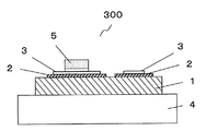
- FIG. 1 is a schematic sectional view showing a power module of the present invention.
- the power module 300 includes a cooler 4, a metal substrate 1, a polyimide resin layer 2, a conductive metal wiring layer 3, and a power semiconductor element 5.
- the power semiconductor element 5 is a semiconductor that controls or supplies power and power, and has a high voltage and large current capacity (output capacity of 100 VA or more and 100 MVA or less) as compared with a normal semiconductor element.
- An element adapted to the operation of the above can be used. Examples thereof include a Schottky barrier diode, a fast recovery diode, a thyristor, a bipolar transistor, a MOSFET, and an IGBT.
- a semiconductor integrated circuit that outputs a desired function in response to a signal from the conductive metal wiring layer 3 is incorporated.
- a control circuit for controlling the output of the power semiconductor element 5 is incorporated in the conductive metal wiring layer 3.
- the power semiconductor element is a wire made of copper, nickel, gold or the like, one end of which is connected to the terminal part, and the other end is wire-bonded to the power semiconductor element (not shown).
- the metal substrate 1 is formed of a material such as a metal having excellent thermal conductivity in order to discharge heat generated from the power semiconductor element 5 mounted via the polyimide resin layer 2.
- the polyimide resin layer 2 is formed in a pattern on the metal substrate 1.
- the cooler 4 the metal substrate 1, the polyimide resin layer 2, the conductive metal wiring layer 3, and the power semiconductor element 5 are sequentially stacked, and the cooler 4 and the metal substrate 1 are sequentially arranged.
- a structure having a stacked region is obtained.
- the polyimide resin layer 2 is an area interposed between the metal substrate 1 and the power semiconductor element 5, and electrically insulates the metal substrate 1 from the power semiconductor element 5 and the conductive metal wiring layer 3. And has a heat conduction function for heat dissipation.
- the metal substrate 1 is made of a material such as a metal having excellent thermal conductivity in order to discharge heat generated from the mounted power semiconductor element 5.
- the polyimide resin layer 2 is formed in a pattern, the metal substrate 1 is exposed in a region where the cooler 4 and the metal substrate 1 of the power module 300 are sequentially laminated, and the heat dissipation effect is great.
- the cooler 4 is fixed and installed with heat conductive grease, a heat radiating adhesive sheet, screws or the like in order to efficiently dissipate heat from the heat source so as to contact the metal substrate 1. It is a component that dissipates the heat to the outside, and is formed of a material with high thermal conductivity such as copper or aluminum and a structure with good cooling properties.
- the heat generated in the power semiconductor element 5 can be easily conducted from the polyimide resin layer 2 to the cooler 4 through the metal substrate 1 and radiated. It becomes possible.
- FIG. 2 is a schematic cross-sectional view showing another embodiment of the power module of the present invention.
- the power module 300 ′ includes a power semiconductor element 5, a conductive metal wiring layer 3, a polyimide resin layer 2, a metal substrate 1, and a cooler 4.
- the polyimide resin layer 2 is formed in a pattern on the metal substrate 1.
- a region where the power semiconductor element 5 is provided on the metal substrate 1 via the polyimide resin layer 2, a cooler 4, the metal substrate 1, and a conductive metal wiring layer are sequentially laminated. And a region in which the cooler 4 and the metal substrate 1 are sequentially laminated.
- the heat generated in the power semiconductor element 5 can be easily conducted to the cooler 4 through the metal substrate 1 and radiated.
- the heat generated from the conductive metal wiring layer can be easily conducted from the polyimide resin layer 2 to the cooler 4 via the metal substrate 1 to be dissipated.
- the metal substrate 1 is exposed and the heat dissipation effect is large.
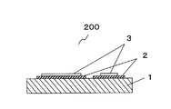
- FIG. 3 is a schematic sectional view showing a substrate 200 with a metal wiring for a power module of the present invention.
- the power module substrate with metal wiring 200 includes a metal substrate 1, a polyimide resin layer 2, and a conductive metal wiring layer 3.
- the polyimide resin layer 2 is formed in a pattern on the metal substrate 1. The function of each layer is the same as described in FIG.
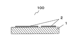
- FIG. 4 is a schematic cross-sectional view showing a power module substrate of the present invention.
- the power module substrate 100 includes a metal substrate 1 and a polyimide resin layer 2.
- the polyimide resin layer 2 is formed in a pattern on the metal substrate 1.
- the metal substrate supports the polyimide resin layer and the conductive metal wiring layer, and has thermal conductivity.
- having thermal conductivity means that the thermal conductivity of the metal substrate at room temperature (300 K) is 10 W / mK or more.
- the metal substrate may be a single layer or a laminate composed of a plurality of layers, but in the case of a laminate, it means that each layer is 10 W / mK or more. Therefore, when the metal substrate is a laminate, the heat conductive adhesive layer or the adhesive sheet, specifically, the copper-heat conductive adhesive layer or the adhesive sheet-aluminum three-layer structure.
- the heat conductive adhesive layer is also included in the metal substrate in the present invention when the heat conductivity is 10 W / mK or more.
- the higher the value of thermal conductivity the better. More specifically, it is more preferably 50 W / mK, particularly preferably 100 W / mK or more, and more preferably 200 W / mK or more. Further preferred.
- the linear thermal expansion coefficient of the metal substrate is preferably in the range of 0 ppm / ° C. to 25 ppm / ° C. from the viewpoint of dimensional stability.
- the said support base material is cut
- the measurement conditions were a heating rate of 10 ° C./min, a tensile load of 1 g / 25,000 ⁇ m 2 so that the weight per cross-sectional area of the evaluation sample was the same, and an average linear thermal expansion within a range of 100 ° C. to 200 ° C.
- the coefficient is the linear thermal expansion coefficient (C.T.E.).
- any thermal conductive material that can stably support the polyimide resin layer and the conductive metal wiring layer and have a desired thermal conductivity can be used. It is not particularly limited, for example, aluminum, aluminum alloy, copper, copper alloy, phosphor bronze, stainless steel (SUS), gold, gold alloy, nickel, nickel alloy, silver, silver alloy, tin, tin alloy, titanium And metal materials such as iron, iron alloy, zinc, molybdenum and invar, and semiconductor materials such as silicon and graphite.
- aluminum, copper, silver, gold and alloys based on these, silicon, or graphite are preferable. This is because the thermal conductivity is high and the heat dissipation is excellent.
- metal material aluminum, copper, and an alloy containing these as main components are preferable.
- aluminum is particularly preferable from the viewpoint of reducing the weight of the metal substrate.
- Copper is preferable when the metal thickness is large and heat dissipation is important.
- process resistance such as chemical resistance and heat resistance.
- the material is a metal material, copper, silver, and gold are preferable. It is because it has high chemical resistance and heat resistance.
- a metal substrate made of a metal having such a large ionization tendency or an alloy containing the metal as a main component is used.
- a protective layer or the like it is preferable to form and use a protective layer or the like. More specifically, when a metal substrate made of aluminum or an alloy containing aluminum as a main component is included, a protective layer formed on the metal substrate is preferably included. This is because the chemical resistance of the polyimide resin layer can be improved during patterning, and it can be prevented from being attacked by an acidic chemical solution or an alkaline chemical solution, particularly an alkaline chemical solution.
- the material constituting the protective layer is not particularly limited as long as it has a desired chemical resistance, and examples thereof include an alkali-resistant material having a desired alkali resistance, mainly composed of an inorganic material. Can be mentioned.
- the formation location is not particularly limited as long as it is formed so as to cover at least a part of the surface of the metal substrate to be protected, but the polyimide resin layer of the metal substrate is formed in plan view. Of the surface on the side to be formed, it is preferable to include all of the region where the metal substrate is exposed when the polyimide resin layer is patterned. More preferably, the entire surface is preferable, and the entire surface of the metal substrate is more preferable. This is because, when the formation location is the above-described region, it is possible to effectively suppress erosion caused by an alkali developer and an etching solution used when patterning the polyimide resin layer.
- the metal substrate is a laminate and has an adhesive layer that improves the adhesion with the polyimide resin layer on the polyimide resin layer side surface
- it is not particularly limited as long as it has a thermal conductivity of 5 and can improve the adhesion to the polyimide resin layer, and can be made of the above-mentioned thermally conductive material.
- the thickness can be in the range of 1 nm to 1000 nm, for example.
- the value of the thermal conductivity of the adhesive layer is relatively smaller than the material mainly constituting the metal substrate, it is preferably 1 nm to 500 nm, preferably 1 nm to 100 nm. More preferably. If it is more than that, the process takes time and costs become high.
- the shape of the metal substrate is not particularly limited, and even if the shape is a flat shape and controlled by a surface roughness with a nanometer order period, the cross-sectional shape of the metal substrate is in contact with the cooler.
- corrugation in a surface or a contact surface with a polyimide-type resin layer may be sufficient.
- the surface area increases.
- the adhesion is good, the thermal diffusion is good, and the heat dissipation can be improved.
- the surface area is increased, and the adhesion is improved by the anchor effect. Further, the exposed portion of the metal surface on which the polyimide resin layer is patterned has increased adhesion with the sealing material due to anchor curing with the sealing resin, thereby improving reliability.
- the height of the irregularities is preferably 0.2 ⁇ m or less because the filler component is clogged, that is, there is a risk of reducing the insulation.
- a method for forming irregularities for example, a method of directly embossing, etching, sandblasting, frosting, stamping, etc.
- a method of forming an irregular pattern using a photoresist, etc., plating A method is mentioned.
- embossing for example, a rolling roll having irregularities on the surface may be used.
- etching processing a chemical is selected according to the type of metal substrate.
- embossing and etching are preferably used from the viewpoint of cost.
- the unevenness width, pitch, and the like are appropriately selected according to the type of metal substrate, the application of the present invention, and the like, and a range suitable for heat conduction can be obtained by simulation, for example.
- the thickness of the metal substrate is not particularly limited as long as it has thermal conductivity, and is appropriately selected according to the use of the power module.
- the thicker the metal substrate the better the thermal diffusion in the surface direction. That is, by making the heat capacity of the metal substrate large, it becomes possible to easily diffuse the local heat at the part in contact with the element, lower the maximum temperature of the part, and prevent damage to the element. As a result, heat dissipation can be improved.
- the present invention when it is used for a power semiconductor element having a large calorific value, it may be anything that can exhibit particularly excellent heat dissipation, and specifically, it may be 1 mm to 5 mm. preferable. This is because when the thickness is in the above-described range, excellent heat dissipation can be achieved.
- the metal substrate may have a protective layer for improving adhesion with the polyimide resin layer, preventing rust, and chemical resistance.
- the soot protective layer is effective in protecting the chemical solution during the manufacturing process, protecting the chemical solution that may ooze out from the module sealing resin from acid and base, and improving the adhesion to the polyimide resin layer.
- the method for forming the protective layer is not particularly limited as long as it is a method that can be stably formed on the surface of the supporting substrate, but rust preventive treatment, plating treatment, anodizing (alumite) treatment, Alternatively, a method using chemical conversion treatment, that is, the metal substrate protective layer is preferably an oxide layer formed by anodizing treatment, an oxide layer or sulfide layer formed by chemical conversion treatment, or a plating layer.
- the thickness is preferably 1 ⁇ m or more. Among them, the thickness is preferably 5 ⁇ m or more, and particularly preferably 10 ⁇ m or more.
- the polyimide resin layer patterning method forms a resist pattern on the polyimide film obtained by imidizing the polyimide resin precursor.
- the metal substrate can be stably protected even with an extremely strong alkaline solution such as an etching solution or a resist stripping solution used in the case of patterning by etching and then stripping the resist.
- the protective layer may be subjected to a surface treatment such as unevenness like the metal substrate. Or you may make it follow the unevenness
- about an upper limit since it is preferable from the viewpoint that alkali resistance can be improved, so that it is thick, there is no particular limitation. However, since the cost increases as the thickness increases, it is usually set to 100 ⁇ m or less.
- a plating method As a plating method, a commonly used plating method can be used. Specifically, a wet plating method (electrolytic plating method or electroless plating method), a dry plating method (vacuum deposition method, sputtering method, metallicon method). ) Etc. can be used. Among them, the wet plating method is preferable, and the electrolytic plating method is particularly preferable. This is because a denser plating layer can be formed. Further, as a result, even when the thickness is thin, the alkali resistance can be sufficiently improved. Moreover, in the wet plating, the plating speed is fast, so that the plating time can be shortened.
- Electroplating used as a wet plating method is a method in which a substance (metal) is electrically connected to the surface of a conductive object by passing a direct current through an electrolytic solution containing the substance to be plated, using the conductive object as a cathode. Etc.) is reduced and deposited to form a layer.
- the metal in the case of performing electroplating is not particularly limited as long as it is a metal with higher chemical resistance than the metal substrate to be protected and has high adhesion to the polyimide resin layer, manganese, zinc, chromium, iron, Examples thereof include cadmium, cobalt, nickel, tin, lead, bismuth, copper, silver, palladium, iridium, platinum, gold, gallium, ruthenium, rhodium, indium, and osmium.
- nickel plating since nickel plating has a dense surface, it is preferable from the viewpoint of preventing rust, improving the adhesion to the polyimide resin layer, and cost.
- the substance in the solution containing the substance to be plated, the substance (on the surface of the object to be plated (electrically) by the electrons released by the oxidation of the reducing agent contained in the solution, not the electrons caused by energization. A metal or the like) is reduced and deposited to form a layer.
- the electroless plating method has the advantage that the film thickness unevenness can be reduced, and since the conductivity is not required for the object to be plated at the time of plating, the object for forming the metal substrate protective layer is made of aluminum or aluminum. Even if it is a metal base material which consists of an alloy which has a main component, it has the advantage that it can be set as a thing with few plating irregularities.
- the metal in the case of performing electroless plating is not particularly limited as long as it is a metal having higher chemical resistance than the metal substrate to be protected, and is not limited to cadmium, cobalt, nickel, tin, lead, bismuth, copper, silver, Examples include palladium, platinum, gold, ruthenium, rhodium, and indium.
- Dry plating is a method in which a metal, oxide, nitride, or the like is gasified, ionized, or liquefied and then deposited on the surface of the material.
- the metal for dry plating is not particularly limited as long as it is a metal with higher chemical resistance than the metal substrate to be protected.
- the metal base is made of aluminum or an alloy containing aluminum as a main component.
- the dry plating method not only metals but also metals and non-metal oxides and nitrides can be stacked.
- oxides of metals such as Cr, Zn, In, Ga, Cd, Ti, Sn, Te, Mg, W, Mo, Cu, Al, Fe, Sr, Ni, Ir, Mg, Si,
- a film made of a non-metallic oxide such as Ge or B, or a nitride, sulfide, selenide, or mixture of the above elements can be formed.
- a conductive object is used as an anode in an electrolytic solution, and a direct current is passed to electrically oxidize the conductive object to form an oxide layer (oxide film layer) on the surface. It is to be formed.
- the electrolytic solution in the case of anodizing is not particularly limited as long as it can form an oxide film having a sufficient thickness on the metal substrate to be protected, a sulfuric acid bath, an oxalic acid bath, a chromic acid bath, An acidic bath such as a phosphoric acid bath, an alkaline bath such as a sodium hydroxide bath and an ammonia bath can be used.
- Chemical conversion treatment uses a chemical reaction such as oxidation or sulfidization in solution to chemically react with the surface of the support substrate to form a corrosion-resistant film such as an oxide layer (oxide film) or sulfide layer (sulfide film). It is a method to do.
- a corrosion-resistant film such as an oxide layer (oxide film) or sulfide layer (sulfide film).
- Such chemical conversion treatment has an advantage that the corrosion-resistant film can be easily formed on the entire surface (including the end surface) because it can be formed without connecting the electrodes.
- the solution for the chemical conversion treatment is not particularly limited as long as it can form a corrosion-resistant film having a sufficient thickness on the supporting base material to be protected. Phosphoric acid / chromate, chromate Type, alkali / chromate type, boehmite type, zirconium type, zinc phosphate type and the like.
- the material constituting the metal substrate is a metal material because the processing is easy in a photolithography method, a method of directly processing by laser, punching, or the like. It is because the metal substrate having the metal substrate protective layer can be easily formed by forming the metal substrate protective layer by such a method.
- the conductive metal wiring layer used in the present invention is formed directly on the polyimide resin layer, and can be electrically connected to the power semiconductor element disposed on the power module substrate of the present invention. Usually, it includes a conductive layer made of a conductive material. In the present invention, the conductive metal wiring layer is used as appropriate before and after pattern formation.
- the material used for the conductive metal wiring layer is not particularly limited as long as it is a conductive material, and is appropriately selected depending on the presence or absence of transparency.
- a conductive material For example, Al, Au, Ta, W, Pt, Ni, Pd, Cr, Cu, Mo, simple metals such as alkali metals and alkaline earth metals, oxides of these metals, Al alloys such as AlLi, AlCa and AlMg, Mg alloys such as MgAg, Ni alloys , Cr alloys, alkali metal alloys, alkaline earth metal alloys, and the like.
- These conductive materials may be used alone, in combination of two or more kinds, or may be laminated using two or more kinds.
- conductive oxides such as indium tin oxide (ITO), indium zinc oxide (IZO), tin oxide, zinc oxide, indium oxide, and aluminum zinc oxide (AZO) can also be used.
- the electrical resistivity is preferably 1.0 ⁇ 10 ⁇ 6 ⁇ ⁇ m or less, more preferably 1.0 ⁇ 10 ⁇ 7 ⁇ ⁇ m or less, More preferably, it is 3.0 ⁇ 10 ⁇ 8 ⁇ ⁇ m. This is because in the case of flowing a large current, the effect of suppressing the loss becomes remarkable, and heat generation can be reduced.
- the thickness of the conductive metal wiring layer is appropriately set according to the use of the substrate with metal wiring for power module of the present invention.
- 100 ⁇ m to 500 ⁇ m is preferable from the viewpoint of preventing short circuit due to heat generation and easy heat dissipation from the conductive metal wiring layer.
- 100 ⁇ m is preferable.
- ⁇ 300 ⁇ m is preferred.
- the conductive metal wiring layer includes a conductive layer made of the conductive material. If necessary, the conductive metal wiring layer has an adhesion layer for improving the adhesion to the polyimide resin layer on the polyimide resin layer side surface, and an electron. It may have a protective layer such as a plating layer for preventing oxidative deterioration of the conductive metal wiring layer on the surface where the element is disposed.
- the adhesion layer is not particularly limited as long as the adhesion between the polyimide resin layer and the conductive metal wiring layer can be improved, but the adhesion layer used for the support substrate is not limited. Can be similar.
- examples of the plating layer include tin, nickel, silver, and gold plating layers. Further, a nickel plating layer may be formed as a base for the gold plating layer. The thickness of the plating layer can be in the range of 0.01 ⁇ m to 4.0 ⁇ m, for example.
- the method for forming the conductive metal wiring layer is not particularly limited as long as the conductive metal wiring layer is formed directly on the polyimide resin layer.
- the method and conditions for providing a metal layer by the metallization method on the polyimide resin layer are not particularly limited, and any method of thermocompression bonding, vapor deposition, sputtering, and plating may be used. Further, a method of combining a plurality of these methods may be used. Specifically, when the adhesive layer is included, first, an adhesive layer made of an inorganic material is formed on the polyimide resin layer by sputtering or the like, and then the conductive layer is formed by vapor deposition or plating. A method of forming a layer can be used.
- the surface of the conductive metal wiring layer may be roughened or roughened, and chemical processing, plasma processing, embossing, etching, sandblasting, frosting, stamping, etc.
- embossing for example, a rolling roll having irregularities on the surface may be used.
- etching processing a chemical is selected according to the type of metal substrate. Note that the unevenness width, pitch, and the like are appropriately selected according to the type of metal substrate, the application of the present invention, and the like, and a range suitable for heat conduction can be obtained by simulation, for example.
- a general method can be used. For example, a method of depositing the conductive material through a mask, or forming the conductive metal wiring layer. Then, a method of etching using a resist can be used.
- a method of depositing the conductive material through a mask, or forming the conductive metal wiring layer. Then, a method of etching using a resist can be used.
- the polyimide resin layer of the present invention is configured to include at least one thermoplastic polyimide resin layer.
- the polyimide resin layer preferably includes a non-thermoplastic polyimide resin layer in addition to the thermoplastic polyimide resin layer.
- the order is determined in consideration of the above physical properties of the thermoplastic polyimide resin layer and the non-thermoplastic polyimide resin layer.
- the non-thermoplastic polyimide resin layer is first formed of the conductive metal layer for the metal substrate or conductive metal wiring layer. It is formed on the surface of the conductive metal layer for the metal substrate or the conductive metal wiring layer after the layer containing the thermoplastic resin is formed on the surface by the direct coating method, etc. Are preferably formed.
- thermoplastic polyimide resin layer is first formed on a metal substrate and a conductive metal layer, and a layer containing a non-thermoplastic insulating resin is used as an intermediate layer. After being formed and finally forming a layer containing a thermoplastic resin, it is formed by being in close contact with the surface of the conductive metal layer for the metal substrate or the conductive metal wiring layer and bonded by a heating and pressing method.
- substrate with a metal wiring for modules excellent in insulation and adhesiveness is obtained.
- the conductive metal wiring layer or metal substrate and the polyimide precursor chemically interact to contact each other at the interface.
- heat transfer is improved and heat dissipation is improved, and the heat dissipation and heat resistance of the power module is achieved by constructing a material that has a small difference between the linear thermal expansion and the conductive metal wiring layer and metal substrate.
- substrate with a metal wiring for power modules which eliminates the restriction
- Chemical interaction refers to the interaction with the surface of the conductive metal wiring layer or metal substrate without providing an adhesive layer.
- the hydroxyl group, carbonyl group, or amino group in the polyimide precursor is the conductive metal wiring layer. It interacts electrically with the surface of the metal substrate and increases the adhesion to the conductive metal wiring layer and the surface of the metal substrate even after heat curing, and eliminates contact resistance and improves heat dissipation. .
- thermoplastic polyimide resin that can be thermocompression bonded, and adheres well to metal substrates or conductive metal wiring layers by heating and pressurizing, so there is no deterioration in insulation due to peeling or cracking, and heat dissipation. Good effect can be obtained.
- the thermoplastic polyimide resin layer is 4 times thinner than the non-thermoplastic polyimide resin layer, which adversely affects the film thickness change due to linear thermal expansion and softening, dimensional change of the conductive metal wiring layer, and insulation. It is hard to affect.
- the non-thermoplastic polyimide resin layer has a small linear expansion due to the linear expansion of the metal substrate and the conductive metal wiring layer. As a result, the effect of improving the reliability can be obtained.
- the glass transition temperature (Tg) of the polyimide resin layer as a whole is preferably 260 ° C. or higher, and particularly preferably 270 ° C. or higher from the viewpoint of heat resistance. It is because the heat resistance of the module substrate of the present invention can be made sufficiently high when the Tg is within the above range. The higher the Tg, the better the heat resistance, but it is usually preferable to cure (heat treatment) at a temperature higher than the Tg in order to bring out the physical properties of the polyimide. There is a possibility that the resin layer and the metal substrate deteriorate. From such a viewpoint, the upper limit of Tg is preferably 500 ° C. or lower.
- the temperature at which the polyimide resin layer begins to soften is around 250 ° C. or lower, and it is in an environment such as an engine room or around an element with a high temperature process such as solder reflow or a high temperature at start-up. This is because the polyimide resin layer may begin to soften, and accordingly, insulation, heat dissipation, and adhesion may be deteriorated. Conversely, when Tg is higher than the above range, the temperature at which softening starts is high, so that the thermal stress cannot be sufficiently relaxed, or the polyimide resin layer, the metal substrate, etc. may be deteriorated. .
- the polyimide resin layer preferably has no melting point at 260 ° C. or lower, more preferably has no melting point at 270 ° C. or lower, and more preferably has no melting point at 300 ° C. or lower. It is because the heat resistance of the board with metal wiring for modules of the present invention can be made sufficiently high.
- the total thickness of the polyimide resin layer 2 is in the range of 20 ⁇ m to 150 ⁇ m, exhibits desired insulation, prevents short circuit between the metal substrate and the conductive metal wiring layer, and exhibits desired heat dissipation.
- the voltage it is not particularly limited, and is set according to the required withstand voltage.
- the voltage used is less than 4 k, it is 20 ⁇ m to 70 ⁇ m, more preferably 20 ⁇ m to 50 ⁇ m from the viewpoint of heat dissipation. In the case of about 4 kV, it is preferably 20 ⁇ m to 100 ⁇ m, and preferably 20 ⁇ m to 70 ⁇ m from the viewpoint of heat dissipation.
- the voltage used is about 6 kV, it is preferably 20 ⁇ m to 150 ⁇ m, preferably 20 ⁇ m to 100 ⁇ m from the viewpoint of heat dissipation and peeling. If it is more than 10 kV, 40 ⁇ m to 150 ⁇ m is preferable from the viewpoint of withstand voltage. Further, the thermal conductivity at this time is preferably 1 W / mK to 13 W / mK, and preferably 2.5 W / mK to 13 W / mK from the viewpoint of thinning and heat dissipation.
- a film having only the polyimide resin layer is prepared for measurement of thermal conductivity.
- a method of peeling the insulating laminate, or after producing a polyimide resin layer on a metal plate the metal plate is removed by etching, and a polyimide resin layer There is a method of obtaining the film.
- the obtained film of the polyimide resin layer is cut into a width of 30 mm and a length of 30 mm to obtain an evaluation sample.
- a blackening material carbon spray
- the thermal conductivity ⁇ is the specific heat Cp, the thermal diffusivity ⁇ , and the density ⁇ of the test piece.
- the product ⁇ ⁇ ⁇ Cp ⁇ ⁇ was obtained.
- the linear thermal expansion coefficient of the polyimide-based resin layer 2 is within the range of 0 ppm / ° C. to 40 ppm / ° C. from the viewpoint of heat dissipation and insulation due to peeling and cracking when using the power wiring board for power modules of the present invention. Preferably there is. This is because if the linear thermal expansion coefficient is too large, the expansion and contraction that occurs when the temperature changes is increased, which adversely affects the above viewpoint. Moreover, even if it is a case where what consists of metal materials excellent in heat dissipation, such as copper and aluminum, is used as said metal substrate, generation
- the difference between the linear thermal expansion coefficient of the polyimide resin layer 2 and the linear thermal expansion coefficient of the metal substrate 1 and the conductive metal wiring layer 3 is preferably 15 ppm / ° C. or less from the viewpoint of peeling and cracking. More preferably, it is 10 ppm / ° C. or less, and further preferably 5 ppm / ° C. or less.
- the substrate with metal wiring for power module 200 is preferably not peeled in a temperature environment in the range of 0 ° C. to 100 ° C., preferably 0 ° C. to 150 ° C., 0 ° C. to 260 ° C. If the difference in linear thermal expansion coefficient between the polyimide resin layer 2 and the metal substrate 1 is greatly different because the polyimide resin layer 2 has a large linear thermal expansion coefficient, the power module substrate with metal wiring 200 changes in the thermal environment. Will peel off.
- the linear thermal expansion coefficient is measured as follows. First, a film having only the polyimide resin layer is prepared. After producing a film consisting only of a polyimide resin layer on a metal plate, after removing the insulating laminate, or after producing a polyimide resin layer on a metal plate, the metal plate is removed by etching. There is a method of obtaining a resin layer film. Next, the obtained polyimide resin layer film is cut into a width of 5 mm and a length of 20 mm to obtain an evaluation sample. The linear thermal expansion coefficient is measured by a thermomechanical analyzer (for example, Thermo Plus TMA8310 manufactured by Rigaku Corporation).
- a thermomechanical analyzer for example, Thermo Plus TMA8310 manufactured by Rigaku Corporation.
- the measurement conditions were a heating rate of 10 ° C./min, a tensile load of 1 g / 25,000 ⁇ m 2 so that the weight per cross-sectional area of the evaluation sample was the same, and an average linear thermal expansion within a range of 100 ° C. to 200 ° C.
- the coefficient is the linear thermal expansion coefficient (C.T.E.).
- the water absorption of the polyimide-based resin layer 2 is preferably relatively small because it can be considered to be a water-based process or a long-term storage in terms of operation and process in a high-humidity environment.
- One index of water absorption is the hygroscopic expansion coefficient. Therefore, it is preferable that the hygroscopic expansion coefficient of the polyimide resin layer 2 is as small as possible. Specifically, it is preferably in the range of 0 ppm /% RH to 15 ppm /% RH, more preferably 0 ppm /% RH to 12 ppm. /% RH, more preferably 0 ppm /% RH to 10 ppm /% RH.
- the hygroscopic expansion coefficient of the polyimide resin layer 2 is in the above range, the water absorption of the polyimide resin layer 2 can be sufficiently reduced, and the substrate with metal wiring for power module of the present invention can be easily stored. This is because when the element is manufactured using the substrate with metal wiring for power module, the process becomes simple.
- the smaller the hygroscopic expansion coefficient of the non-thermoplastic polyimide the lower the concern about peeling and cracking of the polyimide resin layer 2.
- the hygroscopic expansion coefficient of the polyimide-based resin layer 2 is large, due to the difference in expansion coefficient from the metal substrate whose hygroscopic expansion coefficient is almost zero, the adhesiveness with the metal substrate and wiring decreases with increasing humidity. Because there are cases.
- a measuring method of a hygroscopic expansion coefficient it can measure with a humidity variable mechanical analyzer (Thermo Plus TMA8310 by Rigaku).
- the tensile weight is set to 1 g / 25000 ⁇ m 2 so that the weight per cross-sectional area of the evaluation sample becomes the same.
- the glass transition temperature (Tg) of the polyimide resin constituting the polyimide resin layer 2 is preferably 260 ° C. or higher, and particularly preferably 270 ° C. or higher from the viewpoint of heat resistance. It is because the heat resistance of the board with a metal wiring for a power module of the present invention can be made sufficiently high when the Tg is within the above range.
- Tg is higher than the above range, the temperature at which softening begins is high, so the thermal stress cannot be sufficiently relaxed, or the polyimide resin layer 2 and the metal substrate 1 may be deteriorated.
- the polyimide resin layer 2 does not have a melting point at 260 ° C. or less, more preferably it does not have a melting point at 270 ° C. or less, and further preferably does not have a melting point at 300 ° C. or less. .
- the heat resistance of the power wiring board for power module of the present invention can be made sufficiently high.
- Thermoplastic polyimide resin layer Specifically, as the thermoplastic polyimide resin constituting the polyimide resin layer 2, the storage elastic modulus in the temperature range from room temperature (about 25 ° C.) to 300 ° C. or the glass transition temperature + 20 ° C., whichever is lower. Is a polyimide resin that is always less than 1.0 ⁇ 10 8 Pa.
- the storage elastic modulus in the temperature range from room temperature (about 25 ° C.) to 300 ° C. or the glass transition temperature + 20 ° C., whichever is lower, is particularly limited as long as it is always less than 1.0 ⁇ 10 8 Pa.
- the thermoplastic polyimide resin is in the range of 9.0 ⁇ 10 7 Pa to 1.0 ⁇ 10 5 Pa, and more preferably 5.0 ⁇ 10 7 Pa to 1. It is preferably within the range of 0 ⁇ 10 5 Pa.
- the metal substrate 1 or the conductive metal wiring layer 3 is difficult to stick by thermocompression bonding, and a gap is generated between the polyimide resin layer and peeling during a long-term operation. Occurs and leads to deterioration of reliability.
- a polyimide resin layer having a storage elastic modulus of 1.0 ⁇ 10 8 Pa or more is always used in a temperature range from room temperature (about 25 ° C.) to 300 ° C. or a glass transition temperature + 20 ° C., whichever is lower.
- the polyimide resin layer of less than 1.0 ⁇ 10 8 Pa is laminated on the surface that is in contact with the metal substrate 1 or the conductive metal wiring layer 3 or the surface of the metal layer that is necessarily thermocompression bonded.
- the thickness of the polyimide resin layer of less than 1.0 ⁇ 10 8 Pa to be laminated is not particularly specified, but is preferably 25% or less of the polyimide resin layer of 1.0 ⁇ 10 8 Pa or more from the viewpoint of the thermal expansion coefficient. .
- the storage elastic modulus is a value measured using a dynamic viscoelasticity measuring device (for example, RSA3 manufactured by TA Instruments) under the conditions of a frequency of 1 Hz and a heating rate of 5 ° C./min.
- a dynamic viscoelasticity measuring device for example, RSA3 manufactured by TA Instruments
- the polyimide resin is aromatic from the viewpoint of making the heat resistance, linear thermal expansion coefficient, hygroscopic expansion coefficient, thermal conductivity, and storage elastic modulus of the polyimide resin layer 2 suitable for the power module substrate of the present invention.
- a polyimide resin containing a skeleton is preferable.
- polyimide resins polyimide resins containing aromatic skeletons are derived from their rigid and highly planar skeletons, which have excellent heat resistance and insulation properties in thin films, high thermal conductivity, and linear thermal expansion. It is because it is preferably used for the polyimide resin layer 2 of the power module substrate with metal wiring 200 because the coefficient is low.
- R 1 is a tetravalent organic group
- R 2 is a divalent organic group
- R 1 and R 2 that are repeated may be the same or different from each other.
- n is a natural number of 1 or more.
- R 1 is a structure derived from tetracarboxylic dianhydride
- R 2 is a structure derived from diamine
- a polyimide resin is composed of tetracarboxylic dianhydride and It is obtained by reacting diamine to synthesize a polyimide resin precursor such as polyamic acid and then imidizing it thermally or chemically. That is, the polyimide resin precursor is a compound in the previous stage where the polyimide resin is produced.
- the tetracarboxylic dianhydride preferably used from the viewpoints of the heat resistance and linear thermal expansion coefficient of the polyimide resin is an aromatic tetracarboxylic dianhydride.
- Particularly preferred tetracarboxylic dianhydrides include pyromellitic dianhydride, merophanic dianhydride, 3,3 ′, 4,4′-benzophenone tetracarboxylic dianhydride, 3,3 ′, 4.
- 3,3 ′, 4,4′-biphenyltetracarboxylic dianhydride, 2,3,3 ′, 4′-biphenyltetracarboxylic dianhydride, 2,3 2,2 ′, 3′-biphenyltetracarboxylic dianhydride and bis (3,4-dicarboxyphenyl) ether dianhydride are particularly preferred.
- the tetracarboxylic dianhydride into which fluorine is introduced is used as the tetracarboxylic dianhydride used in combination, the hygroscopic expansion coefficient of the polyimide resin is lowered.
- a polyimide resin precursor having a fluorine-containing skeleton is difficult to dissolve in a basic aqueous solution and needs to be developed with a mixed solution of an organic solvent such as alcohol and a basic aqueous solution.
- pyromellitic dianhydride merophanic dianhydride, 3,3 ′, 4,4′-biphenyltetracarboxylic dianhydride, 2,3,3 ′, 4′-biphenyltetracarboxylic dianhydride
- rigid tetracarboxylic dianhydrides such as 2,3,2 ′, 3′-biphenyltetracarboxylic dianhydride and 1,4,5,8-naphthalenetetracarboxylic dianhydride are used, Since the linear thermal expansion coefficient of resin becomes small, it is preferable.
- the polyimide resin contains any structure of the above formula, it is derived from these rigid skeletons and exhibits low linear thermal expansion and low hygroscopic expansion. There is also an advantage that it is easily available on the market and is low in cost.
- the polyimide resin having the structure as described above is a polyimide resin exhibiting high heat resistance and a low linear thermal expansion coefficient. Therefore, the content of the structure represented by the above formula is preferably closer to 100 mol% of R 1 in the formula (I), but at least 33 mol% or more of R 1 in the formula (I). It may be contained. Among them, the content of the structure represented by the above formula is preferably 50 mol% or more, more preferably 70 mol% or more, of R 1 in the formula (I).
- the benzene rings interact with each other to form a core and improve thermal conductivity.
- the skeleton does not become a rigid skeleton, and the linear thermal expansion coefficient and humidity expansion coefficient may decrease.
- the polyimide resin having the structure as described above is a polyimide resin showing an improvement in thermal conductivity. Therefore, the content of the structure represented by the above formula may be at least 33 mol% or more of R 1 in the above formula (I). Further, in this case, it is used in combination with a tetracarboxylic acid having a rigid skeleton so that the glass transition temperature does not become 260 ° C. or lower.
- the polyimide resin having the above structure in combination with pyromellitic dianhydride, good etching properties can be obtained with respect to an alkaline etching solution of polyimide.
- the amount of pyromellitic dianhydride is 50 mol% to 90 mol% with respect to the acid dianhydride used in combination. From the viewpoint of suppressing humidity expansion, when the tetracarboxylic dianhydride has an alicyclic skeleton, the transparency of the polyimide resin precursor is improved, so that a highly sensitive photosensitive polyimide resin can be obtained.
- the polyimide resin is used in combination with a tetracarboxylic acid having an aromatic skeleton of 33 mol% or more.
- a diamine component applicable to the polyimide resin one kind of diamine can be used alone, or two or more kinds of diamines can be used in combination.
- the diamine component used is not particularly limited. For example, p-phenylenediamine, m-phenylenediamine, o-phenylenediamine, 3,3′-diaminodiphenyl ether, 3,4′-diaminodiphenyl ether, 4,4 ′.
- a diamine or the like obtained by substituting a part or all of the hydrogen atoms on the aromatic ring of the diamine with a substituent selected from a fluoro group, a methyl group, a methoxy group, a trifluoromethyl group, or a trifluoromethoxy group. Can do.
- the polyimide resin in order to make the polyimide resin have a storage elastic modulus that expresses a desired thermoplasticity, two or more kinds of diamines as raw materials constituting the polyimide resin contained as a main component are mixed.
- the one or more diamines preferably contain a flexural raw material ratio of 50 mol% or more, and may be block copolymerization or random polymerization.
- random polymerization in which amines are randomly arranged is storage elastic modulus. From the viewpoint of.
- the amino group is preferably meta-coordinated from the viewpoint of lowering the storage elastic modulus and improving the adhesion, and n is preferably 1 to 3 from the viewpoint of heat resistance.
- the diamine component to be used is not particularly limited.
- DANPG 1,3-bis (4-aminophenoxy) -2,2-dimethylpropane
- BAPP 2,2-bis [4- (4-aminophenoxy) phenyl] propane
- APB 3-bis (3-aminophenoxy) benzene
- p-PDA paraphenylenediamine
- DPE 3,4'-diaminodiphenyl ether
- ODA 4,4'-diaminodiphenyl ether
- the diamine can be selected depending on the desired physical properties. If a rigid diamine such as p-phenylenediamine is used, the polyimide resin has a low expansion coefficient.
- rigid diamines include p-phenylenediamine, m-phenylenediamine, 1,4-diaminonaphthalene, 1,5-diaminonaphthalene, 2,6 as diamines in which two amino groups are bonded to the same aromatic ring. -Diaminonaphthalene, 2,7-diaminonaphthalene, 1,4-diaminoanthracene and the like.
- diamines in which two or more aromatic rings are bonded by a single bond, and two or more amino groups are each bonded directly or as part of a substituent on a separate aromatic ring for example, Some are represented by the following formula (II). Specific examples include benzidine and the like.
- a is a natural number of 0 or 1 or more, and the amino group is bonded to the meta position or the para position with respect to the bond between the benzene rings.
- a diamine having a substituent at a position where the amino group on the benzene ring is not substituted without being involved in the bond with other benzene rings can also be used. These substituents are monovalent organic groups, but they may be bonded to each other.
- R 3 is a divalent organic group, an oxygen atom, a sulfur atom, or a sulfone group, and R 4 and R 5 are a monovalent organic group or a halogen atom.
- the polyimide resin contains any structure of the above formula, it is derived from these rigid skeletons and exhibits low linear thermal expansion and low hygroscopic expansion. Furthermore, there is also an advantage that it is easily available on the market and is low cost.
- p-phenylenediamine, m-phenylenediamine, 1,4-diaminonaphthalene, etc. are rigid diamines such as p-phenylenediamine in which two amino groups are bonded to the same aromatic ring. 1,5-diaminonaphthalene, 2,6-diaminonaphthalene, 2,7-diaminonaphthalene, 1,4-diaminoanthracene and the like.
- R 3 in [Chemical Formula 4] is a divalent organic group, an oxygen atom, a sulfur atom, or a sulfone group
- R 4 and R 5 are a monovalent organic group or a halogen atom.
- the compound of [Chemical Formula 4] and diamines in which one benzene ring is inserted with a divalent organic group, oxygen atom, sulfur atom, or sulfone group between two benzene rings having an amino group are also included.
- the content of the structure represented by the above formula may be at least 33 mol% or more of R 2 in the above formula (I).
- Diamine compounds such as 4,4′-diamino-2,2′-dimethylbiphenyl and 4,4′-diaminodiphenyl ether have good etchability with an alkaline etchant, and contain 33 mol% or more of paraphenylenediamine, 4,4 ′
- -diamino-2'-methoxybenzanilide or the like it is possible to expect the effect of exhibiting good etching property and low thermal expansion.
- Solvents used in the varnish solution are generally N-methylpyrrolidone (NMP), methylformamide (DMF), dimethylacetamide (DMAc), dimethyl sulfoxide (DMSO), dimethyl sulfate, sulfolane, butyrolactone, Examples include cresol, phenol, halogenated phenol, cyclohexane, dioxane, tetrahydrofuran, diglyme, and triglyme.
- NMP N-methylpyrrolidone
- DMF methylformamide
- DMAc dimethylacetamide
- DMSO dimethyl sulfoxide
- sulfate dimethyl sulfate
- sulfolane butyrolactone
- Examples include cresol, phenol, halogenated phenol, cyclohexane, dioxane, tetrahydrofuran, diglyme, and triglyme.
- the method for forming the non-thermoplastic polyimide resin layer is not particularly limited as long as it can be directly formed on a metal substrate or a conductive metal wiring layer (before wiring formation). Extrusion molding, application, etc.
- a spin coating method for example, a spin coating method, a die coating method, a dip coating method, a bar coating method, a gravure printing method, a screen printing method, or the like can be used.
- Non-thermoplastic polyimide-based resins are those that do not have thermoplasticity, that is, those that do not exhibit plasticity at a temperature at which a general thermoplastic polyimide exhibits thermoplasticity, specifically,
- the storage elastic modulus in the temperature range from room temperature (about 25 ° C.) to 300 ° C. or the glass transition temperature + 20 ° C., whichever is lower, is particularly limited as long as it is always 1.0 ⁇ 10 8 Pa or more. Although not intended, it is preferably within the range of 1.0 ⁇ 10 8 Pa to 1.0 ⁇ 10 11 Pa, and more preferably within the range of 5.0 ⁇ 10 8 Pa to 5.0 ⁇ 10 10 Pa. Preferably there is.
- the polyimide resin layer may begin to soften during high-temperature processes such as solder reflow, so the film thickness changes during heating, the dimensions of the conductive metal wiring layer change, This is because the insulating property may be deteriorated by the change in thickness.
- a polyimide is only a polyimide-type resin layer which has thermoplasticity, it is necessary to use the monomer (mainly diamine) of a flexible frame
- the storage elastic modulus when the storage elastic modulus is higher than the above range, it is difficult to soften the film to a level at which it is easy to relieve thermal stress during baking, which has an adverse effect on the distortion of the polyimide resin layer and the surface flatness. There is a possibility of effect.
- the storage elastic modulus of a polyimide when the storage elastic modulus of a polyimide is a high thing, it is necessary to use the monomer (mainly diamine) of rigid frame
- the linear expansion coefficient becomes too small and it becomes difficult to match the metal layer.
- the storage elastic modulus is a value measured using a dynamic viscoelasticity measuring apparatus (for example, RSA3 manufactured by TA Instruments) under conditions of a frequency of 1 Hz and a heating rate of 5 ° C./min.
- a dynamic viscoelasticity measuring apparatus for example, RSA3 manufactured by TA Instruments
- thermoplastic polyimide resin in the present application is usually less than 1.0 ⁇ 10 8 Pa in storage modulus in a temperature range from room temperature (about 25 ° C.) to 300 ° C. or the glass transition temperature + 20 ° C., whichever is lower. This means a polyimide having a temperature range of
- the glass transition temperature (Tg) of the non-thermoplastic polyimide resin is not particularly limited as long as it can exhibit desired insulation properties, but is preferably 260 ° C. or higher. It is desirable that it is 270 ° C. or higher from the viewpoint of heat resistance. It is because the heat resistance of the power module substrate of the present invention can be made sufficiently high when the Tg is within the above range.
- the resin layer and the metal substrate may be deteriorated.
- the upper limit of Tg is preferably 500 ° C. or lower.
- Tg is lower than the above range, the temperature at which the polyimide resin layer begins to soften is around 250 ° C. or lower, and the polyimide resin layer may begin to soften during high-temperature processes such as solder reflow. This is because there is a possibility that the insulation properties deteriorate due to the change in the film thickness and the dimensional change of the conductive metal wiring layer.
- Tg is higher than the above range, the temperature at which softening begins is high, so the thermal stress cannot be sufficiently relaxed, or the polyimide resin layer, the substrate with metal wiring for power modules, etc. may deteriorate. Because there is.
- the non-thermoplastic polyimide resin in the present invention preferably has no melting point at 260 ° C. or lower, preferably has no melting point at 270 ° C. or lower, and has no melting point at 300 ° C. or lower. More preferably. This is because the heat resistance of the power wiring board for power module of the present invention can be made sufficiently high.
- the thermal conductivity of the non-thermoplastic polyimide resin layer is not particularly limited as long as it can provide desired thermal conductivity.
- the thermal conductivity of the non-thermoplastic polyimide resin layer is preferably 1 W / mK to 15 W / mK. Furthermore, 2.5 W / mK to 15 W / mK is preferable from the viewpoint of thinning and heat dissipation.
- the coefficient of linear thermal expansion of the non-thermoplastic polyimide resin is within the range of 0 ppm / ° C. to 40 ppm / ° C. from the viewpoint of heat dissipation and insulation due to peeling or cracking when using the substrate with metal wiring for power module of the present invention. It is preferable that This is because if the linear thermal expansion coefficient is too large, the expansion and contraction that occurs when the temperature changes is increased, which adversely affects the above viewpoint. Further, even when the metal substrate is made of a metal material excellent in heat dissipation such as copper or aluminum, the occurrence of peeling or warping can be sufficiently suppressed.
- the linear thermal expansion coefficient is measured as follows. First, a film made of only the non-thermoplastic polyimide resin is prepared. After producing a film (polyimide resin layer) consisting only of the non-thermoplastic polyimide resin on the metal, a method of peeling the polyimide resin layer, or producing the non-thermoplastic polyimide film on the metal substrate. Thereafter, there is a method of removing the metal by etching to obtain the non-thermoplastic polyimide resin film. Next, the obtained non-thermoplastic polyimide resin film is cut into a width of 5 mm and a length of 20 mm to obtain an evaluation sample.
- the linear thermal expansion coefficient is measured by a thermomechanical analyzer (for example, Thermo Plus TMA8310 (manufactured by Rigaku Corporation)).
- the measurement conditions were a heating rate of 10 ° C./min, a tensile load of 1 g / 25,000 ⁇ m 2 so that the weight per cross-sectional area of the evaluation sample was the same, and an average linear heat within a range of 100 ° C. to 200 ° C.
- the expansion coefficient be the linear thermal expansion coefficient (C.T.E.).
- the difference between the coefficient of linear thermal expansion of the non-thermoplastic polyimide resin and the coefficient of linear thermal expansion of the metal is 15 ppm / ° C. or less from the viewpoint of not adversely affecting heat dissipation and insulation due to peeling or cracking. Is preferable, more preferably 10 ppm / ° C. or less, and further preferably 5 ppm / ° C. or less.
- peeling and cracking of the power module metal wiring substrate of the present invention are suppressed, and when the thermal environment of the power module metal wiring substrate is changed, This is because the stress at the interface with the metal substrate is reduced and the adhesion is improved.
- the substrate with metal wiring for power module of the present invention is not peeled off in the temperature environment of 0 ° C. to 100 ° C., preferably 0 ° C. to 150 ° C., 0 ° C. to 260 ° C. in handling.
- the power wiring substrate for the power module will change in the thermal environment. It will peel off due to the difference in expansion coefficient.
- the water absorption of the non-thermoplastic polyimide resin is preferably relatively small because it can be considered to be an aqueous process or long-term storage in terms of operation and process in a high humidity environment.
- One index of water absorption is the hygroscopic expansion coefficient. Therefore, the moisture absorption expansion coefficient of the non-thermoplastic polyimide resin is preferably as small as possible. Specifically, it is preferably in the range of 0 ppm /% RH to 15 ppm /% RH, more preferably 0 ppm /% RH. Within the range of ⁇ 12 ppm /% RH, more preferably within the range of 0 ppm /% RH to 10 ppm /% RH.
- the hygroscopic expansion coefficient of the non-thermoplastic polyimide resin is in the above range, the water absorption of the non-thermoplastic polyimide resin can be sufficiently reduced, and the power wiring board for power modules of the present invention can be easily stored. This is because when the power semiconductor element module is manufactured using the power module substrate with metal wiring, the process becomes simple.
- the smaller the hygroscopic expansion coefficient of the non-thermoplastic polyimide resin the better the adhesion between the conductive metal wiring layer or metal substrate and the non-thermoplastic polyimide resin, and to heat dissipation and insulation due to peeling and cracking. Does not adversely affect.
- a measuring method of a hygroscopic expansion coefficient it can measure with a humidity variable mechanical analyzer (Thermo Plus TMA8310 by Rigaku).
- the tensile weight is set to 1 g / 25000 ⁇ m 2 so that the weight per cross-sectional area of the evaluation sample becomes the same.
- the linear thermal expansion coefficient, hygroscopic expansion coefficient, thermal conductivity, and storage elastic modulus of the polyimide resin layer are suitable for the power module substrate of the present invention.
- a polyimide resin containing an aromatic skeleton is preferable.
- polyimide resins polyimide resin containing an aromatic skeleton is derived from its rigid and highly planar skeleton, has excellent heat resistance and insulation properties in thin films, and its molecular constituent parts continuously vibrate. It is because it is preferably used for the polyimide resin layer of the power module substrate of the present invention because of its high conductivity and low linear thermal expansion coefficient.
- R 1 is a tetravalent organic group
- R 2 is a divalent organic group
- R 1 and R 2 that are repeated may be the same or different from each other.
- n is a natural number of 1 or more.
- R 1 is a structure derived from tetracarboxylic dianhydride
- R 2 is a structure derived from diamine
- a polyimide resin is composed of tetracarboxylic dianhydride and diamine. Is synthesized to synthesize a polyimide precursor such as polyamic acid and then imidized thermally or chemically.
- tetracarboxylic dianhydrides applicable to the polyimide resin include ethylene tetracarboxylic dianhydride, butane tetracarboxylic dianhydride, cyclobutane tetracarboxylic dianhydride, and cyclopentane tetracarboxylic dianhydride.
- the tetracarboxylic dianhydride preferably used from the viewpoints of the heat resistance and linear thermal expansion coefficient of the polyimide resin is an aromatic tetracarboxylic dianhydride.
- Particularly preferred tetracarboxylic dianhydrides include pyromellitic dianhydride, merophanic dianhydride, 3,3 ′, 4,4′-benzophenone tetracarboxylic dianhydride, 3,3 ′, 4.
- 3,3 ′, 4,4′-biphenyltetracarboxylic dianhydride, 2,3,3 ′, 4′-biphenyltetracarboxylic dianhydride, 2,3 2,2 ′, 3′-biphenyltetracarboxylic dianhydride and bis (3,4-dicarboxyphenyl) ether dianhydride are particularly preferred.
- the tetracarboxylic dianhydride into which fluorine is introduced is used as the tetracarboxylic dianhydride used in combination, the hygroscopic expansion coefficient of the polyimide resin is lowered.
- a polyimide resin precursor having a fluorine-containing skeleton is difficult to dissolve in a basic aqueous solution and needs to be developed with a mixed solution of an organic solvent such as alcohol and a basic aqueous solution.
- pyromellitic dianhydride merophanic dianhydride, 3,3 ′, 4,4′-biphenyltetracarboxylic dianhydride, 2,3,3 ′, 4′-biphenyltetracarboxylic dianhydride
- rigid tetracarboxylic dianhydrides such as 2,3,2 ′, 3′-biphenyltetracarboxylic dianhydride and 1,4,5,8-naphthalenetetracarboxylic dianhydride are used
- polyimide resin Is preferable because the coefficient of linear thermal expansion is small.
- the polyimide resin contains any structure of the above formula, it is derived from these rigid skeletons and exhibits low linear thermal expansion and low hygroscopic expansion. There is also an advantage that it is easily available on the market and is low in cost.
- the polyimide resin having the structure as described above is a polyimide resin exhibiting high heat resistance and a low linear thermal expansion coefficient. Therefore, the content of the structure represented by the above formula is preferably closer to 100 mol% of R 1 in the formula (I), but at least 33 mol% or more of R 1 in the formula (I). It may be contained. Among them, the content of the structure represented by the above formula is preferably 50 mol% or more, more preferably 70 mol% or more, of R 1 in the formula (I).
- a tetracarboxylic dianhydride containing one benzene ring connected with is used, benzene rings in other adjacent molecules interact with each other to form a core and improve thermal conductivity.
- the skeleton does not become a rigid skeleton, and the linear thermal expansion coefficient and humidity expansion coefficient may decrease.
- the polyimide resin having the structure as described above is a polyimide resin that exhibits improved thermal conductivity. Therefore, the content of the structure represented by the above formula may be at least 33 mol% or more of R 1 in the above formula (I). Further, in this case, pyromellitic acid 2 which is a tetracarboxylic acid having a rigid skeleton within a range of 1.0 ⁇ 10 8 Pa to 1.0 ⁇ 10 11 Pa and having a glass transition temperature of 260 ° C. or lower.
- the diamine component applicable to the polyimide resin can be used alone or in combination of two or more diamines.
- the diamine component used is not particularly limited.
- a diamine or the like obtained by substituting a part or all of the hydrogen atoms on the aromatic ring of the diamine with a substituent selected from a fluoro group, a methyl group, a methoxy group, a trifluoromethyl group, or a trifluoromethoxy group. Can do.
- the diamine can be selected depending on the desired physical properties. If a rigid diamine such as p-phenylenediamine is used, the polyimide resin has a low expansion coefficient.
- rigid diamines include p-phenylenediamine, m-phenylenediamine, 1,4-diaminonaphthalene, 1,5-diaminonaphthalene, 2,6 as diamines in which two amino groups are bonded to the same aromatic ring. -Diaminonaphthalene, 2,7-diaminonaphthalene, 1,4-diaminoanthracene and the like.
- diamines in which two or more aromatic rings are bonded by a single bond, and two or more amino groups are each bonded directly or as part of a substituent on a separate aromatic ring for example, Some are represented by the following formula (II). Specific examples include benzidine and the like.
- a is a natural number of 0 or 1 or more, and the amino group is bonded to the meta position or the para position with respect to the bond between the benzene rings.
- a diamine having a substituent at a position where the amino group on the benzene ring is not substituted without being involved in the bond with other benzene rings can also be used. These substituents are monovalent organic groups, but they may be bonded to each other.
- polyimide resin precursors containing fluorine, especially polyamic acid are difficult to dissolve in a basic aqueous solution.
- the polyimide resin precursor is processed during the processing.
- R 3 is a divalent organic group, an oxygen atom, a sulfur atom, or a sulfone group, and R 4 and R 5 are a monovalent organic group or a halogen atom.
- the polyimide resin contains any structure of the above formula, it is derived from these rigid skeletons and exhibits low linear thermal expansion and low hygroscopic expansion. Furthermore, there is also an advantage that it is easily available on the market and is low cost.
- the heat resistance of a polyimide resin improves and a linear thermal expansion coefficient becomes small. Therefore, the closer to 100 mol% of R 2 in the above formula (I), the better, but it is sufficient to contain at least 33 mol% of R 2 in the above formula (I).
- the content of the structure represented by the above formula is preferably 50 mol% or more, more preferably 70 mol% or more, of R 2 in the formula (I).
- p-phenylenediamine, m-phenylenediamine, 1,4-diaminonaphthalene, etc. are rigid diamines such as p-phenylenediamine in which two amino groups are bonded to the same aromatic ring. 1,5-diaminonaphthalene, 2,6-diaminonaphthalene, 2,7-diaminonaphthalene, 1,4-diaminoanthracene and the like.
- R 3 in [Chemical Formula 4] is a divalent organic group, an oxygen atom, a sulfur atom, or a sulfone group
- R 4 and R 5 are a monovalent organic group or a halogen atom.
- the compound of [Chemical Formula 4] and diamines in which one benzene ring is inserted with a divalent organic group, oxygen atom, sulfur atom, or sulfone group between two benzene rings having an amino group are also included.
- the content of the structure represented by the above formula may be at least 33 mol% or more of R 2 in the above formula (I).
- p-phenylenediamine and m-phenylenediamine are used as rigid diamines in the range of 1.0 ⁇ 10 8 Pa to 1.0 ⁇ 10 11 Pa and the glass transition point is not lower than 260 ° C.
- the non-thermoplastic polyimide resin in order to make the non-thermoplastic polyimide resin have a desired storage elastic modulus, about tetracarboxylic dianhydride and diamine which are raw materials constituting the polyimide-based resin contained as a main component, It is preferable that the ratio of the raw material having flexibility is small. That is, it is preferable that the tetracarboxylic dianhydride constituting the polyimide resin and the tetracarboxylic dianhydride having a flexible structure in the diamine and the content of the diamine having a flexible structure are small.
- the tetracarboxylic dianhydride having a flexible structure is not particularly limited as long as it has a flexible skeleton and has a low storage elastic modulus and Tg. Fundamentals and Applications, Ikuo Imai, Rikio Yokota, NTS, p. 241-252 (2002), Latest Trends in Rapid Progressing Polyimide IV, Sumibe Research Co., Ltd., p. 3 to 12, and those described in WO2007 / 015396.
- the viscosity of the obtained polyimide resin is preferably 2000 mPa ⁇ s to 100,000 mPa ⁇ s. More preferably, it is 3000 mPa ⁇ s to 30000 mPa ⁇ s, and if it is less than that, the film becomes fragile and cannot be formed, which adversely affects Tg reduction and insulation. Beyond that, a flat film cannot be formed.
- the viscosity was measured using a TV-22 viscometer manufactured by Toki Sangyo.
- Terminal groups may be introduced according to the purpose, such as improving the patterning property of the precursor, crosslinking, and dispersibility with the filler, at the terminal of the resulting polyimide resin.
- the conductive metal wiring layer or metal substrate and the polyimide precursor will chemically interact, eliminating contact resistance at the interface. With good heat transfer, heat dissipation is improved. And, by forming a material with low thermal expansion and good adhesion to the conductive metal wiring layer and metal substrate, the power module has heat dissipation and heat resistance. Power module metal that improves reliability, enables the fabrication of large-area power modules, and reduces the bonding layer to simplify the structure of the power module and eliminate restrictions on the soldering process temperature during chip bonding A substrate with wiring can be provided.
- Chemical interaction refers to the interaction with the surface of the conductive metal wiring layer or metal substrate without providing an adhesive layer.
- the hydroxyl group, carbonyl group, or amino group in the polyimide precursor is the conductive metal wiring layer. It interacts electrically with the surface of the metal substrate and increases the adhesion to the conductive metal wiring layer and the surface of the metal substrate even after heat curing, and eliminates contact resistance and improves heat dissipation. .
- a polyimide resin precursor used for pattern formation of a polyimide resin layer has a chemical formula of [Chemical Formula 5] having an amino group and a carboxyl group generated by a ring-opening addition reaction of diamine to tetracarboxylic dianhydride. It refers to a polyamic acid having a repeating structure.
- the polyimide resin precursor dissolves in a polar solvent and is easy to handle as a varnish, and has a carboxyl group, so that it is easily dissolved not only in an organic solvent but also in a basic aqueous solution as a developer.
- the polyimide resin precursor becomes a polyimide resin having a repeating structure of the chemical formula [Chemical Formula 6] having an imide group obtained by intramolecular dehydration reaction of an amino group and a carboxyl group by heat treatment or a catalyst.
- a polyimide resin By using a polyimide resin, various properties such as insulation and heat resistance effective in the present invention, and solvent resistance that is insoluble or hardly soluble in an organic solvent or an acid-base aqueous solution can be obtained.
- the terminal of the compound of the polyimide resin precursor may be sealed with a terminal sealing agent.
- the end-capping agent is not particularly limited as long as it is an acid anhydride that can seal the end group of the polyimide resin, but a compound having an acid anhydride group is a viewpoint for improving the developability of the polyimide resin precursor.
- phthalic anhydride alkyl group-containing phthalic anhydride (4-methylphthalic anhydride, 3-methylphthalic anhydride, 4-tert-butylphthalic anhydride, etc.), halogenated phthalic anhydride ( 4-chlorophthalic anhydride, 4,5-dichlorophthalic anhydride, tetrachlorophthalic anhydride, 4-bromophthalic anhydride, tetrabromophthalic anhydride, 4-fluorophthalic anhydride, 3-fluorophthal Acid anhydride, tetrafluorophthalic anhydride, etc.), carboxy-containing phthalic anhydride (4-carboxyphthalic anhydride, etc.), 3,4,5,6-te Lahydrophthalic anhydride, hexahydrophthalic anhydride, 4-methylhexahydrophthalic anhydride, vinyl group-containing phthalic anhydride (4-vinylphthalic anhydride, 3-vinylphthalic anhydride, vinyl
- the hydrogen atom on the aromatic ring may be substituted with an alkyl group having 1 to 6 carbon atoms, an alkenyl group, an alkynyl group, an alkoxyl group, or a halogen atom.
- end capping agents may be used alone or in combination of two or more.
- the method for sealing the polymer terminal of the polyamic acid with an acid anhydride is not particularly limited, but the following methods are exemplified.
- a method of polymerizing a polyimide resin precursor having an amino group as a terminal, and reacting an acid anhydride with a polymer 2) A method of using, as a part of the raw material, a diamine obtained by reacting one of the two amino groups with an acid anhydride in an amount corresponding to a molecular weight assumed in advance.
- a polyimide resin precursor having a molecular weight adjusted in advance so as to have a predetermined viscosity can be used, so that the viscosity of the end-capped polyimide resin precursor solution is controlled. There is a merit that it is easy.
- the method 2) uses a diamine previously reacted with an acid anhydride as a part of the raw material, so that there is a merit that an acid anhydride residue is introduced into a polymer terminal at a relatively high rate after polymerization.
- the amount of terminal group derived from the end capping agent introduced by adding these end capping agents is not particularly limited, The amount is preferably 10 mol% or more, more preferably 30 mol% to 100 mol%, more preferably 50 mol% to 100 mol%, and preferably 67 mol% to 100 mol% with respect to the end group amount of the polyimide before the end-capping agent is added. Further preferred.
- the number average molecular weight of the polyimide resin precursor is preferably 10,000 to 500,000, more preferably 12,000 to 300,000, and more preferably 15,000 to 300,000 from the viewpoints of solubility, end-capping effect, film brittleness, coatability, and developability of the precursor. 100000 is most desirable.
- For the measurement of the number average molecular weight there is a method using a terminal group quantification method from a substituent at the polymer terminal and a substituent at the main chain by NMR measurement. There is also a measurement method that utilizes the fact that the vapor pressure, osmotic pressure, and boiling point of a solution depend on its molarity and molarity. In the present invention, the number average molecular weight was calculated by a method of quantifying end groups by 1HNMR.
- the polyimide resin precursor can be developed with a basic aqueous solution from the viewpoint of ensuring the safety of the working environment and reducing the process cost when patterning the polyimide resin layer on the metal substrate.
- the basic aqueous solution can be obtained at a lower cost than the organic solvent and can be produced at a lower cost because the waste liquid treatment cost and the equipment cost for ensuring work safety are low.
- the pattern formation method is to laminate a photoresist on the polyimide precursor and irradiate with ionizing radiation through a photomask, or draw a pattern with ultraviolet, visible or infrared light directly with laser or LED.
- the photoresist and the polyimide resin precursor are developed using the photoresist as a mask.
- the pattern may be rinsed with water as necessary and dried at 80 ° C. to 100 ° C. to stabilize the pattern. Furthermore, it heat-processes and imidizes and it is set as the polyimide resin which formed the pattern.
- Ionizing radiation refers to charged particles of electrons, protons, ⁇ particles, ultraviolet rays, X-rays, and ⁇ rays. Thereafter, conductive metal wiring is formed on the patterned polyimide resin.
- the polyimide resin precursor is coated, dried, and imidized to form a polyimide resin.
- a photoresist is laminated on the entire surface of the conductive metal wiring, and ionizing radiation is emitted through a photomask. Irradiation or patterning of ultraviolet, visible, or infrared light is directly performed with a laser or LED, and the polyimide resin is etched with an alkaline etchant using the photoresist as a mask. After forming the pattern, the photoresist is peeled off.
- the polyimide resin precursor is coated, dried, and imidized to form a polyimide resin, and a photoresist is laminated on the entire surface of the polyimide resin and irradiated with ionizing radiation through a photomask, or ultraviolet, visible, red Either external light may be directly drawn with a laser or LED, the polyimide resin may be etched with an alkaline etchant, and after forming the pattern, the photoresist may be peeled off to form a conductive metal wiring.
- alkali etching solution examples include alkali-amine etching solutions and the like, which can be suitably used, but are not particularly limited.
- a commercially available product is TPE-3000: trade name, manufactured by Toray Engineering Co., Ltd.
- an alkaline aqueous solution is desirable, and it is preferable to use a basic chemical solution having a pH of 9 or more, more preferably 11 or more.
- an organic alkali may be sufficient and an inorganic alkali may be sufficient, and also the mixed form of the 2 types may be sufficient.
- the etchant temperature is preferably between 0 ° C. and 110 ° C. The lower the temperature, the slower the etching rate, and the higher the temperature, the concentration changes due to boiling and the workability and the etching rate change. A range is more preferable.
- the photosensitive polyimide resin used for pattern formation of the polyimide resin layer is a photosensitive polyimide resin having a polyimide component and a photosensitive agent that becomes a polyimide resin after imidization such as heat treatment. Even what is obtained may be obtained using a polyimide resin precursor obtained by adding a photosensitizer as an imidation catalyst, and there is no particular limitation. Moreover, there is no limitation of positive type or negative type.
- the photosensitive polyimide resin for example, an ethylenic double bond is introduced into the carboxyl group of the polyimide resin precursor by an ester bond or an ionic bond, and a photo radical initiator is used as a photosensitive agent in the resulting polyimide resin precursor. It can mix and can be set as a solvent development negative photosensitive polyimide resin. Also, for example, a naphthoquinone diazide compound is added as a photosensitizer to polyamic acid or a partially esterified product thereof to make an alkali development positive photosensitive polyimide resin, or a nifedipine compound is added to a polyimide resin precursor as a photosensitizer to form an alkali.
- a photobase generator can be added to the polyimide resin precursor as a photosensitizer, such as a development negative photosensitive polyimide resin, to obtain an alkali development negative photosensitive polyimide resin.
- photosensitive polyimide resins are added with 15 to 35 parts by weight of a photosensitive agent with respect to 100 parts by weight of the polyimide component. Therefore, even if heating is performed at 300 ° C. to 400 ° C. after pattern formation, a residue derived from the photosensitive agent remains in the polyimide resin. Since these residual materials cause the linear thermal expansion coefficient and the hygroscopic expansion coefficient to increase, peeling and warping occur when using photosensitive polyimide resin compared to when using non-photosensitive polyimide resin. It tends to be easy to do.
- a photosensitive polyimide resin in which a photobase generator is added as a photosensitive agent to a polyimide resin precursor can be patterned even if the addition amount of the photobase generator as a photosensitive agent is 15 parts by weight or less. Therefore, there is little decomposition residue derived from the photosensitizer even after the polyimide resin is used, and there is little deterioration in characteristics such as linear thermal expansion coefficient and hygroscopic expansion coefficient, and there is also little outgas, so it can be applied to the present invention.
- the photosensitive polyimide resin solution can be obtained by adding a photobase generator to the polyimide resin precursor.
- the photobase generator carbazole, quaternary ammonium salt, piperidine and the like can be used as appropriate.
- the photosensitive polyimide resin is not particularly limited as a developer after exposure, as long as a solvent that changes the solubility of the exposed part is used as the developer.
- the basic aqueous solution is not particularly limited.
- TMAH tetramethylammonium hydroxide
- aqueous solution having a concentration of 0.01% by mass to 10% by mass, preferably 0.05% by mass to 5% by mass.
- TMAH tetramethylammonium hydroxide
- the developer may be one type or two or more types, and may contain an organic solvent or the like as long as it contains water at 50% by mass or more, more preferably 70% by mass or more.
- the organic solvent is not particularly limited, but polar solvents such as N-methyl-2-pyrrolidone, N, N-dimethylformamide, N, N-dimethylacetamide, dimethyl sulfoxide, ⁇ -butyrolaclone, dimethylacrylamide, methanol, Alcohols such as ethanol and isopropanol, esters such as ethyl acetate and propylene glycol monomethyl ether acetate, ketones such as cyclopentanone, cyclohexanone, isobutyl ketone and methyl isobutyl ketone, other tetrahydrofuran, chloroform, acetonitrile and the like alone or Two or more types may be added in combination. After development, washing is performed with water or a poor solvent. Also in this case, alcohols such as ethanol and isopropyl alcohol, esters such as ethyl lactate and propylene glycol monomethyl ether acetate may be added to water.
- Examples of the developing method include a spray method, a liquid piling method, a dipping method, and a rocking dipping method.
- ionizing radiation is irradiated through a photomask, or one of ultraviolet, visible, and infrared light (depending on the photosensitive agent) is directly drawn with a laser or LED, and developed.
- the pattern may be rinsed with water as necessary and dried at 80 ° C. to 100 ° C. to stabilize the pattern.
- the pattern may be stabilized by rinsing with water or a poor solvent, if necessary, and drying at 80 ° C. to 100 ° C.
- thermosetting by further heating the pattern as necessary.
- a filler can be added to the polyimide resin layer 2.
- the filler added to the polyimide resin is not particularly limited as long as it is an inorganic compound having an insulating property, but is an inorganic compound having an insulating property with a volume resistivity of 10 13 ⁇ / cm or more. Although there is no restriction
- the filler examples include aluminum oxide, magnesium oxide, boron nitride, aluminum nitride, silicon nitride, talc, mica, aluminum hydroxide, barium sulfate, silicon carbide, diamond, and hydroxyapatite.
- aluminum oxide, boron nitride, and aluminum nitride are preferable from the viewpoint of thermal conductivity.
- thermal conductivity aluminum oxide, boron nitride, and aluminum nitride are preferable.
- the particle shape of the filler is not particularly limited, and examples thereof include spherical shapes, crushed shapes, flake shapes, and aggregated particles. Of these, spherical and flake shapes are preferred from the viewpoints of insulation and thermal conductivity. When used alone, it has a good spherical shape, and the specific surface area of the primary particle size is preferably 0.3 m 2 / g to 15 m 2 / g, and further from the viewpoint of dispersibility, 0.4 m 2 / g to 10 m 2. / g. In other shapes, the area in contact with the adjacent filler is difficult to disperse and the insulating properties deteriorate. When using 2 or more types together, it is preferable from the point that a dispersibility improves by using at least 30 volume% or more of the said spherical fillers used individually by 1 type.
- the particle size of the filler is such that the volume average particle size is 0.01 ⁇ m or more and less than 20 ⁇ m from the viewpoint of thermal conductivity and withstand voltage, and preferably from 0.01 ⁇ m to less than 6 ⁇ m from the viewpoint of filling amount and withstand voltage, One type alone or two or more types may be used in combination. Moreover, in order to improve the dispersibility of a filler, what carried out surface treatments, such as a coupling agent, what added the dispersing agent in the polyimide varnish or the polyimide-type resin precursor varnish may be used.
- silane coupling agents include vinyltrimethoxysilane, vinyltriethoxysilane, vinyltris (2-methoxyethoxy) silane, vinyltrichlorosilane, N- (2-aminoethyl) -3-aminopropylmethyldimethoxysilane, N -(2-aminoethyl) -3-aminopropyltrimethoxysilane, 3-aminopropyltriethoxysilane, N-2- (aminoethyl) -3-aminopropyltriethoxysilane, 3-aminopropyltrimethoxysilane, 3 -Aminopropyltriethoxysilane, N-phenyl-3-aminopropyltrimethoxysilane, 3-glycidoxypropyltrimethoxysilane, 3-glycidoxypropyltriethoxysilane, 3-glycidoxypropylmethyldimethoxysilane
- the filler surface may be modified by a coupling reaction of the silane coupling agent with the surface of the inorganic filler contained in the polyimide varnish or the polyimide resin precursor varnish. Thereby, compatibility with the polyimide resin can be enhanced, and the aggregation and dispersion state of the filler can be controlled.
- the filling amount of the filler is 10 volume% to 70 volume% with respect to the polyimide resin or polyimide resin precursor, and preferably 30 volume% to 60 volume% from the viewpoint of film formability, thermal conductivity, and withstand voltage. Good.
- a photosensitive polyimide resin solution is applied on a metal substrate or a conductive metal wiring layer and dried to form a photosensitive polyimide resin layer on the entire surface. After irradiation with ultraviolet rays through a photomask of a desired pattern, a pattern is developed by development. Forming a polyimide resin layer, A polyimide resin precursor solution is applied onto a metal substrate or a conductive metal wiring layer, dried, a photoresist is laminated, and developed after irradiation with ultraviolet rays through a photomask having a desired pattern to provide a resist opening.
- a method for producing a substrate with a metal wiring for power modules having at least a metal substrate, a polyimide resin layer, and a conductive metal wiring layer is a photosensitive polyimide resin precursor exhibiting thermoplasticity on a metal substrate or a conductive metal wiring layer.
- the conductive metal wiring layer is thermocompression bonded, and when the polyimide resin layer is formed on the conductive metal wiring layer, A step of thermocompression bonding to a metal substrate, and a step of forming a conductive metal wiring after pattern exposure and development after forming a photoresist on the conductive metal wiring layer. It is intended to include.
- the power module manufacturing method is performed in the order of (A), (B), (C), (D), and (E).
- a photosensitive polyimide resin solution is applied on the metal substrate 1 and dried to form a photosensitive polyimide resin layer 2 'on the entire surface.
- FIG. 5D shows a power module metal wiring substrate 200 obtained by forming a conductive metal wiring layer 3 on the metal substrate 1 by plating and thermocompression bonding with the polyimide resin layer 2. It is.
- the conductive metal wiring layer 3 is formed by a photolithography method. For example, after a conductive metal layer is provided on the entire surface of the polyimide resin layer 2 obtained from FIG. (C), a photoresist is stacked, and developed after irradiation with ultraviolet rays through a photomask of a wiring pattern to form a resist opening.
- the conductive metal wiring layer 3 can be formed by eluting the conductive metal layer exposed in the opening by etching and peeling and removing the remaining resist.
- FIG. 5E shows a power module obtained by mounting a power semiconductor element and joining a cooler.
- a method for producing a substrate with a metal wiring for power modules having at least a metal substrate, a polyimide resin layer, and a conductive metal wiring layer is a photosensitive polyimide resin precursor exhibiting thermoplasticity on a metal substrate or a conductive metal wiring layer.
- a solution When a solution is applied, dried, heat-treated to form a photosensitive polyimide resin layer on the entire surface, and when the polyimide resin layer is formed on the metal substrate on the patterned polyimide resin layer Thermocompression-bonds the conductive metal wiring layer, and when the polyimide resin layer is formed on the conductive metal wiring layer, a step of thermocompression bonding to the metal substrate, and a photoresist on the conductive metal wiring layer After the pattern is exposed and developed, a step of forming a conductive metal wiring and a pattern exposure of the exposed photosensitive polyimide resin layer under the conductive metal wiring layer are performed.
- the image is intended to include a step of forming the polyimide resin layer of the pattern, a.
- the conductive metal wiring layer is thermocompression bonded
- the step of thermocompression bonding to the metal substrate the formation of a photoresist on the conductive metal wiring layer, pattern exposure and development, and then conductive Forming a metal wiring.
- the method includes a step of thermocompression bonding to the metal substrate and a step of forming a conductive metal wiring after pattern exposure and development after forming a photoresist on the conductive metal wiring layer.
- a manufacturing method of a power module metal wiring substrate having at least a metal substrate, two or more polyimide resin layers, and a conductive metal wiring layer includes at least one layer of heat on the metal substrate and the entire surface of the conductive metal wiring layer.
- a method of manufacturing a power module metal wiring substrate having at least a metal substrate, a polyimide resin layer, and a conductive metal wiring layer includes: a polyimide resin precursor that exhibits thermoplasticity on the entire surface of the metal substrate or the conductive metal wiring layer; Applying a body solution and drying to form a polyimide resin precursor layer; forming a photoresist on the polyimide resin precursor layer; pattern exposure and development; and patterning the polyimide resin precursor.
- thermocompression bonding to the metal substrate when forms is intended to include after pattern exposure after forming a photoresist Kishirube conductive metal wiring layer on the developing, forming a conductive metal wire, the.
- thermocompression bonding to the metal substrate and a step of forming a conductive metal wiring after pattern exposure and development after forming a photoresist on the conductive metal wiring layer.
- (Production Method Example 8) A method for producing a substrate with a metal wiring for a power module having at least a metal substrate, two or more polyimide resin layers and a conductive metal wiring layer, and having at least a thermoplastic polyimide resin layer and a non-thermoplastic polyimide resin layer.
- a step of applying a polyimide resin precursor solution exhibiting thermoplasticity on a metal substrate or conductive metal wiring layer and drying, and one or more non-thermoplastic polyimides on the polyimide resin precursor layer A step of applying and drying a polyimide resin precursor solution, a step of applying and drying a polyimide resin precursor solution exhibiting thermoplasticity on the polyimide resin precursor layer, and a photo on the polyimide resin precursor layer.
- the step of forming a patterned polyimide resin layer by heat-treating the conductive material When a metal wiring layer is thermocompression bonded and the polyimide resin layer is formed on the conductive metal wiring layer, a process of thermocompression bonding to the metal substrate, and a pattern after forming a photoresist on the conductive metal wiring layer Forming a conductive metal wiring after exposure and development.
- a method of manufacturing a power wiring board for a power module having at least a metal substrate, a polyimide resin layer, and a conductive metal wiring layer is a method for producing a polyimide resin precursor having thermoplasticity on the entire surface of a metal substrate or a conductive metal wiring layer.
- a method for producing a substrate with a metal wiring for a power module having at least a metal substrate, two or more polyimide resin layers and a conductive metal wiring layer, and having at least a thermoplastic polyimide resin layer and a non-thermoplastic polyimide resin layer.
- a step of applying a polyimide resin precursor solution showing non-thermoplasticity on a metal substrate or a conductive metal wiring layer and drying, and a polyimide resin precursor showing thermoplasticity on the polyimide resin precursor layer Applying the solution, drying, heat-treating to form a polyimide-based resin layer, and when the polyimide-based resin layer is formed on the metal-based substrate on the polyimide-based resin layer, the conductive metal wiring
- the polyimide resin layer is formed on the conductive metal wiring layer by thermocompression bonding, a step of thermocompression bonding to the metal substrate; and the conductive metal wiring layer
- the exposed polyimide resin layer is etched.
- a step of applying a polyimide resin precursor solution exhibiting thermoplasticity on a metal substrate or conductive metal wiring layer and drying, and one or more non-thermoplastic polyimides on the polyimide resin precursor layer A step of applying and drying a resin-based resin precursor solution, a step of applying a polyimide-based resin precursor solution exhibiting thermoplasticity on the polyimide-based resin precursor layer, drying, and heat-treating to form a polyimide-based resin layer And when the polyimide resin layer is formed on the metal substrate on the polyimide resin layer having a pattern on the polyimide resin layer, When a conductive metal wiring layer is thermocompression bonded and the polyimide resin layer is formed on the conductive metal wiring layer, a step of thermocompression bonding to the metal substrate, and a photoresist is formed on the conductive metal wiring layer After pattern exposure and development, a step of forming conductive metal wiring, and after pattern exposure and development after forming a photoresist on the conductive metal wiring, the exposed polyimide
- a manufacturing method of a power module metal wiring substrate having at least a metal substrate, a polyimide resin layer and a conductive metal wiring layer is a polyimide system having thermoplasticity on the metal substrate or on the entire surface of the conductive metal wiring layer.
- a method for producing a substrate with a metal wiring for a power module having at least a metal substrate, two or more polyimide resin layers and a conductive metal wiring layer, and having at least a thermoplastic polyimide resin layer and a non-thermoplastic polyimide resin layer.
- the method includes a step of thermocompression bonding to the metal substrate and a step of forming a conductive metal wiring after pattern exposure and development after forming a photoresist on the conductive metal wiring layer.
- (Manufacturing method example 14) A method for producing a substrate with a metal wiring for a power module having at least a metal substrate, two or more polyimide resin layers and a conductive metal wiring layer, and having at least a thermoplastic polyimide resin layer and a non-thermoplastic polyimide resin layer.
- a manufacturing method of a power module metal wiring substrate having at least a metal substrate, two or more polyimide-based resin layers and a conductive metal wiring layer includes at least one layer on the metal substrate and the entire surface of the conductive metal wiring layer.
- thermoplastic polyimide resin precursor solution Applying a thermoplastic polyimide resin precursor solution, drying, heat-treating to form a polyimide resin layer, thermocompression bonding the polyimide resin layers, and applying a photoresist on the conductive metal wiring layer
- a step of forming conductive metal wiring, and after pattern exposure and development after forming a photoresist on the conductive metal wiring the exposed polyimide resin layer is removed by etching. The process of forming the said polyimide-type resin layer of pattern shape by this.
- the conductive metal wiring layer is formed on the polyimide-based resin layer with good adhesion, whereby contact resistance
- the polyimide resin layer When drilling a metal substrate in a part where the polyimide resin layer is not laminated, the polyimide resin layer is not laminated, so the polyimide resin layer in the vicinity of the hole will not be peeled or damaged, so heat dissipation and insulation Can be suppressed.
- the present invention is not limited by the example.
- Polyimide resin precursor solution 1 4.0 g (20 mmol) of 4,4′-diaminodiphenyl ether (ODA) and 8.65 g (80 mmol) of paraphenylenediamine (PPD) were put into a 500 ml separable flask, and 200 g of dehydrated N-methyl-2- The mixture was dissolved in pyrrolidone (NMP), and the mixture was stirred with heating while monitoring with a thermocouple so that the liquid temperature became 50 ° C. with an oil bath in a nitrogen stream.
- ODA 4,4′-diaminodiphenyl ether
- PPD paraphenylenediamine
- polyimide precursor solution 2 (Polyimide resin precursor solution 2) Except that the amount of NMP was adjusted so that the reaction temperature and the concentration of the solution were 17% by mass to 19% by mass, the polyimide precursor solution 2 was prepared in the same manner as in Production Example 1 with the compounding ratio shown in Table 1 below. Was synthesized.
- polyimide resin precursor solution 3 Except for adjusting the amount of NMP so that the reaction temperature and the concentration of the solution are 17% by mass to 19% by mass, the polyimide precursor solution 3 was prepared in the same manner as in Production Example 1 with the compounding ratio shown in Table 1 below. Was synthesized.
- pyromellitic dianhydride (PMDA) (35 mmol) 3,3 ′, 4,4′-biphenyltetracarboxylic dianhydride (BPDA) (65 mmol)
- BPDA 4,4′-biphenyltetracarboxylic dianhydride
- DANPG 1,3- Bis (4-aminophenoxy) -2,2-dimethylpropane
- DPE 3,4′-diaminodiphenyl ether
- Polyimide resin precursor solution 4 (Polyimide resin precursor solution 4) Except that the amount of NMP was adjusted so that the reaction temperature and the concentration of the solution were 17% by mass to 19% by mass, the polyimide precursor solution 4 was prepared in the same manner as in Production Example 1 with the compounding ratio shown in Table 1 below. Was synthesized.
- Polyimide resin precursor solution 5 Except for adjusting the amount of NMP so that the reaction temperature and the concentration of the solution are 17% by mass to 19% by mass, the polyimide precursor solution 5 was prepared in the same manner as in Production Example 1 with the compounding ratio shown in Table 1 below.
- the acid dianhydride pyromellitic dianhydride (PMDA) (35 mmol) 3,3 ′, 4,4′-biphenyltetracarboxylic dianhydride (BPDA) (65 mmol)
- BPDA 4,4′-biphenyltetracarboxylic dianhydride
- diamine 4,4 4.0 g (20 mmol) of '-diaminodiphenyl ether (ODA) and paraphenylenediamine (PPD) were used.
- DNCDP ⁇ [(4,5-dimethoxy-2-nitrobenzyl) oxy] carbonyl ⁇ -2,6-dimethylpiperidine
- DNCDP ⁇ [(4,5-dimethoxy-2-nitrobenzyl) oxy] carbonyl ⁇ -2,6-dimethylpiperidine
- Example 1 ⁇ Formation of polyimide resin layer and conductive metal wiring layer> Nickel-plated (1 ⁇ m) 16 cm square copper base material (C1020) with a thickness of 2.5 mm is coated thereon with the photosensitive polyimide resin precursor solution 1 on a 150 mm square by a die coater with a coating width of 150 mm.
- the area was coated with a polyimide resin layer to a thickness of 35 ⁇ m and dried in an oven at 80 ° C. in the atmosphere for 60 minutes.
- the photosensitive polyimide resin precursor solution 1 was coated on the photosensitive polyimide resin precursor solution 1 that had been exposed in the same manner, and dried in an atmosphere of 80 ° C. in the atmosphere for 60 minutes.
- TMAH aqueous tetramethylammonium hydride
- a photosensitive polyimide patterned polyimide resin layer having a thickness of 45 ⁇ 1 ⁇ m.
- a 250 ⁇ m thick copper base material (C1020) is placed on the polyimide resin layer, vacuum pressed at 13 MPa, 15 minutes, 330 ° C., and then a dry film resist is laminated on the 250 ⁇ m thick copper base material. Then, it was exposed through a photomask of the wiring pattern and developed to form a resist layer having openings corresponding to the wiring pattern shape.
- the conductive metal wiring layer having a thickness of 250 ⁇ m is etched using an etching solution of iron chloride (50 ° C., 45 Baume), and the remaining resist layer is peeled off using Arcastep HTO manufactured by Nichigo Morton.
- a conductive metal wiring layer was formed.
- Example 2 ⁇ Formation of polyimide resin layer and conductive metal wiring layer> Nickel-plated (1 ⁇ m) 16 cm square copper base material (C1020) with a thickness of 2.5 mm, and the polyimide resin precursor solution in which 60% by volume of alumina (DAM05 manufactured by Denki Kagaku Kogyo) is added thereto. No.
- a photoresist (NIT430 manufactured by Nichigo Morton Co., Ltd.) is laminated thereon, exposed to 50 mJ / cm 2 in terms of illuminance at a wavelength of 365 nm with a high pressure mercury lamp through a photomask, and then developed with an aqueous solution of tetramethylammonium hydride (TMAH). Thereafter, heat treatment was performed at 350 ° C. for 1 hour in a nitrogen atmosphere (temperature increase rate: 10 ° C./min, natural cooling) to form a photosensitive polyimide patterned polyimide resin layer having a thickness of 50 ⁇ 1 ⁇ m.
- TMAH tetramethylammonium hydride
- a 250 ⁇ m thick copper base material (C1020) is placed on the polyimide resin layer, vacuum pressed at 13 MPa, 15 minutes, 330 ° C., and then a dry film resist is laminated on the 250 ⁇ m thick copper base material. Then, it was exposed through a photomask of the wiring pattern and developed to form a resist layer having openings corresponding to the wiring pattern shape.
- a conductive metal wiring layer having a thickness of 250 ⁇ m was etched (50 ° C., 45 Baume) and disposed using an etching solution of iron chloride.
- a conductive metal wiring layer was formed.
- a dry film resist was laminated on the polyimide resin layer, exposed through a photomask of the wiring pattern, and developed to form a resist layer having an opening matched to the wiring pattern shape.
- chromium sputtering and copper sputtering are sequentially performed to form a base layer having a thickness of 0.3 ⁇ m, and then electrolytic copper plating is performed using an electrolytic copper plating solution. Then, an electrolytic copper plating layer having a thickness of 250 ⁇ m was disposed.
- Example 3 ⁇ Formation of polyimide resin layer and production of conductive metal wiring layer> Nickel-plated (1 ⁇ m) 16 cm square-cut copper base material (C1020) with a thickness of 200 ⁇ m, 1 mm, and 2.5 mm, and a polyimide resin containing 60% by volume of alumina (DAM05 manufactured by Denki Kagaku Kogyo) Precursor solution 3 was coated on a 150 mm square area with a die coater having a coating width of 150 mm so that the film thickness after curing was 40 ⁇ 1 ⁇ m, and was dried in an atmosphere at 80 ° C. for 60 minutes in the air. Thereafter, heat treatment was performed at 350 ° C. for 1 hour in a nitrogen atmosphere (temperature increase rate: 10 ° C./min, natural cooling).
- a 250 ⁇ m thick copper base material (C1020) is placed on the polyimide resin layer, vacuum pressed at 13 MPa, 15 minutes, 330 ° C., and then a dry film resist is laminated on the 250 ⁇ m thick copper base material. Then, it was exposed through a photomask of the wiring pattern and developed to form a resist layer having openings corresponding to the wiring pattern shape.
- a conductive metal wiring layer having a thickness of 250 ⁇ m was etched (50 ° C., 45 Baume) and disposed using an etching solution of iron chloride.
- the remaining resist layer was peeled off using Alcstep HTO manufactured by Nichigo Morton, and then a conductive metal wiring layer was formed. Thereafter, a resist pattern was formed on the conductive metal wiring layer formed with the laminate.
- a polyimide etching solution TPE-3000 manufactured by Toray Engineering Co., Ltd.
- Example 4 ⁇ Formation of polyimide resin layer and production of conductive metal wiring layer> A nickel-plated (1 ⁇ m) copper base material (C1020) is cut into a 16 cm square and a polyimide resin precursor solution 4 is applied to a 150 mm square area on a 300 mm thick die coater with a coating width of 150 mm. The coating was coated to a thickness of 3 ⁇ 1 ⁇ m and dried in an oven at 80 ° C. for 60 minutes in the air.
- a polyimide resin precursor solution 5 to which 60% by volume of alumina (DAM05 manufactured by Denki Kagaku Kogyo Co., Ltd.) is added is coated on a 150 mm square area with a die coater having a coating width of 150 mm, and the film thickness after curing is 40 ⁇ 1 ⁇ m. And then dried in an oven at 80 ° C. under the atmosphere for 60 minutes.
- DAM05 manufactured by Denki Kagaku Kogyo Co., Ltd.
- the polyimide resin precursor solution 4 is again coated on the 150 mm square area with a die coater having a coating width of 150 mm so that the film thickness after curing is 3 ⁇ 1 ⁇ m, in an oven at 80 ° C. in the atmosphere. Dried under 60 minutes.
- a 300 ⁇ m thick substrate coated with a polyimide resin precursor and a 3 mm thick copper substrate coated with a polyimide resin precursor were heat treated in a nitrogen atmosphere at 350 ° C. for 1 hour (temperature increase rate 10 ° C./min, natural Allowed to cool).
- the polyimide resin layers of the heat-treated substrate are stacked so as to face each other, vacuum-pressed at 13 MPa, 15 minutes, 330 ° C., a dry film resist is laminated on the copper substrate on the 300 ⁇ m-thick substrate side, and a wiring pattern
- the resist layer having an opening matched to the wiring pattern shape was formed by exposure through a photomask and development.
- the 300 ⁇ m thick substrate side was etched (50 ° C., 45 Baume) to provide conductive metal wiring.
- a conductive metal wiring layer was formed.
- Example 5 ⁇ Formation of polyimide resin layer and conductive metal wiring layer> A nickel substrate (1 ⁇ m) 16 cm square cut copper base material (C1020) with a thickness of 3 mm and a photosensitive polyimide 1 added with 60% by volume of alumina (DAM05 manufactured by Denki Kagaku Kogyo Co., Ltd.) is coated with a width of 150 mm. Were coated on a 150 mm square area as a polyimide resin layer to 45 ⁇ m and dried in an oven at 80 ° C. in the air for 60 minutes.
- DAM05 photosensitive polyimide 1 added with 60% by volume of alumina
- photosensitive polyimide 2 added with 60% by volume of alumina (DAM05 manufactured by Denki Kagaku Kogyo Co., Ltd.) is coated on a 150 mm square area with a die coater with a coating width of 150 mm so that the polyimide resin layer is 5 ⁇ m. , And dried in an oven at 80 ° C. under the atmosphere for 60 minutes.
- DAM05 manufactured by Denki Kagaku Kogyo Co., Ltd.
- the laminated photosensitive polyimide was exposed to 2000 mJ / cm 2 in terms of illuminance at a wavelength of 365 nm through a photomask through a photomask, heated at 170 ° C. for 10 minutes on a hot plate, and then tetramethylammonium hydride (TMAH ) After development with an aqueous solution, heat treatment was performed at 350 ° C. for 1 hour in a nitrogen atmosphere (temperature increase rate 10 ° C./min, natural cooling), and a patterned polyimide resin layer of photosensitive polyimide having a film thickness of 45 ⁇ 1 ⁇ m Formed.
- TMAH tetramethylammonium hydride
- a 300 ⁇ m thick copper base material (C1020) is placed on the polyimide resin layer and vacuum pressed at 330 ° C. for 15 minutes at 13 MPa, and then a dry film resist is applied on the 300 ⁇ m thick copper base material.
- a resist layer having openings corresponding to the shape of the wiring pattern was formed by laminating, exposing through a photomask of the wiring pattern and developing.
- the conductive metal wiring layer having a thickness of 250 ⁇ m is etched using an etching solution of iron chloride (50 ° C., 45 Baume), and the remaining resist layer is peeled off using Arcastep HTO manufactured by Nichigo Morton Co., Ltd.
- a conductive metal wiring layer was disposed.
- Example 6 ⁇ Dispersion of filler in polyimide resin solution>
- the polyimide resin precursor solution 3 used in Example 3 was diluted with NMP so that the solid content concentration was 16%, and a silane coupling agent (Z-6883 manufactured by Toray Dow Corning Co., Ltd.) was added to 20 g of the varnish.
- Filler treated with silane coupling at 0.5% by mass with respect to the filler (boron nitride filler MGP manufactured by Denki Kagaku Kogyo, alumina filler AL-43-KT manufactured by Showa Denko, AL-47-H, and AL-160SG 13.9 g (60% by volume) with a mass ratio of 50: 45: 3: 2).
- the mixed solution was stirred with a paint shaker for 8 hours to prepare a polyimide resin precursor solution filled with a filler.
- TBHG 2,2′-dimethylbenzidine
- PMDA Pyromellitic anhydride
- the entire surface of the polyimide resin layer forming side is subjected to chromium sputtering and then copper sputtering to form a plating base layer having a thickness of 0.3 ⁇ m, and then electrolytic copper plating is performed using an electrolytic copper plating solution.
- a conductive metal layer made of an electrolytic copper plating layer having a thickness of 250 ⁇ m was disposed.
- an conductive metal wiring layer was formed using an iron (III) chloride aqueous solution (45 Baume).
- a polyimide resin precursor solution was prepared in the same process as in Example 6 except that the heat treatment temperature in a nitrogen atmosphere after application was 250 ° C.
- the polyimide-based resin layer with copper foil produced by the same method as in Examples 2 and 6 and Comparative Example 1 was evaluated for (f) substrate warpage as follows.
- thermomechanical analyzer Thermo Plus Thermo Plus TMA8310
- the measurement conditions are as follows: the observation length of the evaluation sample is 15 mm, the heating rate is 10 ° C./min, the tensile load is 1 g / 25,000 ⁇ m 2 so that the weight per cross-sectional area of the evaluation sample is the same, and 100 ° C. to 200 ° C.
- the average linear thermal expansion coefficient in the range of ° C. was defined as the linear thermal expansion coefficient (CTE).
- the tensile load was set to 1 g / 25000 ⁇ m 2 so that the weight per cross-sectional area of the evaluation sample was the same.
- FIGS. 6 (a) and 6 (b) were formed on a copper foil having a thickness of 18 [mu] m in the same process as in Example 2 and Example 6.
- Example 6 was formed to prepare a polyimide resin layer with copper foil, that is, a power module substrate.
- Comparative Example 1 has no pattern.
- the polyimide resin layer with copper foil was cut into a width of 30 mm and a length of 50 mm to obtain a sample for substrate warpage evaluation.
- FIG. 6A is a plan view showing a polyimide resin layer with copper foil for warpage evaluation test
- FIG. 6B is a cross-sectional view taken along line AA ′ of FIG. 6A. It is.
- a sample is fixed to the surface of a SUS plate, which is a measuring jig, with a polyimide resin layer on the upper surface and only one of the short sides of the sample with Kapton (registered trademark, the same shall apply hereinafter) tape.
- Kapton registered trademark, the same shall apply hereinafter
- the distance from the SUS plate on the short side on the opposite side of the sample was measured when left in a constant temperature and humidity chamber for 1 hour.
- a sample having a distance of 0 mm or more and 0.5 mm or less was evaluated as “ ⁇ ”
- a sample of more than 0.5 mm and 1.0 mm or less was evaluated as ⁇
- a sample of 1.0 mm or more was determined as “X”.
- the polyimide resin layer with a copper foil obtained in the same process as in Example 6 is patterned on a copper base (5 patterns of 150 mm ⁇ 26 mm strips).
- FIG. 7A is a plan view showing a polyimide resin layer with a copper foil for V-groove processing evaluation test
- FIG. 7B is a cross-sectional view taken along line BB ′ of FIG. 7A. It is.
- FIGS. 8A and 8B a polyimide resin layer with a copper foil was prepared by providing a solid polyimide resin layer over the entire surface.
- FIG. 8A is a plan view showing a polyimide resin layer with a copper foil for a V-groove processing comparison test
- FIG. 8B is a cross-sectional view of CC ′ in FIG. 8A. It is sectional drawing.
- V-groove processing with a depth of 1 mm was performed using a V-groove processing cutter under the conditions of a blade angle of 60 °, a rotation speed of about 20 krpm, and a scanning speed of about 0.6 m / min.
- FIG. 7C is a cross-sectional view taken along the line B-B ′ of FIG. 7A (after V-groove processing).
- FIG. 8C is a cross-sectional view taken along the line C-C ′ of FIG. 8A (after V-groove processing).
- Table 2 shows the evaluation results.
Landscapes
- Engineering & Computer Science (AREA)
- Microelectronics & Electronic Packaging (AREA)
- Power Engineering (AREA)
- Physics & Mathematics (AREA)
- Condensed Matter Physics & Semiconductors (AREA)
- General Physics & Mathematics (AREA)
- Computer Hardware Design (AREA)
- Manufacturing & Machinery (AREA)
- Chemical & Material Sciences (AREA)
- Materials Engineering (AREA)
- Insulated Metal Substrates For Printed Circuits (AREA)
- Cooling Or The Like Of Semiconductors Or Solid State Devices (AREA)
Abstract
L'invention concerne un module de puissance sur lequel est monté un élément à semi-conducteur de puissance et qui possède une efficacité de dissipation de chaleur et une fiabilité améliorées au moyen d'un substrat pour modules de puissance, une couche de résine de polyimide étant formée sur un substrat métallique afin d'obtenir aussi bien l'isolation électrique que la conductivité thermique, un substrat à câblage métallique pour modules de puissance qui utilise ce substrat pour modules de puissance, et un procédé de fabrication d'un substrat à câblage métallique pour modules de puissance. Un substrat à câblage métallique pour modules de puissance, qui comprend au moins un substrat métallique, une couche de résine de polyimide et une couche de câblage métallique conductrice, est caractérisé en ce que la couche de résine de polyimide est formée en un motif sur le substrat métallique et en ce qu'un module de puissance utilise ce substrat à câblage métallique pour modules de puissance, un substrat pour modules de puissance pour ce substrat à câblage métallique pour modules de puissance, et un procédé de fabrication d'un substrat à câblage métallique pour modules de puissance.
Applications Claiming Priority (2)
| Application Number | Priority Date | Filing Date | Title |
|---|---|---|---|
| JP2014194674A JP6032254B2 (ja) | 2013-10-11 | 2014-09-25 | パワーモジュール用金属配線付基板、パワーモジュール及びパワーモジュール用基板、並びにパワーモジュール用金属配線付基板の製造方法 |
| JP2014-194674 | 2014-09-25 |
Publications (1)
| Publication Number | Publication Date |
|---|---|
| WO2016047181A1 true WO2016047181A1 (fr) | 2016-03-31 |
Family
ID=55587550
Family Applications (1)
| Application Number | Title | Priority Date | Filing Date |
|---|---|---|---|
| PCT/JP2015/060515 WO2016047181A1 (fr) | 2014-09-25 | 2015-04-02 | Substrat à câblage métallique pour modules de puissance, module de puissance, substrat pour modules de puissance et procédé de fabrication de substrat à câblage métallique pour modules de puissance |
Country Status (2)
| Country | Link |
|---|---|
| JP (1) | JP6032254B2 (fr) |
| WO (1) | WO2016047181A1 (fr) |
Cited By (2)
| Publication number | Priority date | Publication date | Assignee | Title |
|---|---|---|---|---|
| JP2019065265A (ja) * | 2017-09-29 | 2019-04-25 | 日鉄ケミカル&マテリアル株式会社 | ポリイミドフィルム及び金属張積層体 |
| TWI683604B (zh) * | 2016-12-23 | 2020-01-21 | 德商德國艾托特克公司 | 於接觸墊上形成可焊接焊料沉積物的方法及在活化接觸墊上暴露可焊接焊料沉積物之印刷電路板 |
Families Citing this family (3)
| Publication number | Priority date | Publication date | Assignee | Title |
|---|---|---|---|---|
| JP6734531B2 (ja) * | 2016-03-09 | 2020-08-05 | 富士通株式会社 | 電子部品の製造方法、半導体装置の製造方法、及び半導体装置 |
| JP7115868B2 (ja) * | 2018-02-23 | 2022-08-09 | 三井化学株式会社 | 装置 |
| JP2023001636A (ja) | 2021-06-21 | 2023-01-06 | 株式会社ピーアイ技術研究所 | 感光性ポリイミド樹脂組成物 |
Citations (7)
| Publication number | Priority date | Publication date | Assignee | Title |
|---|---|---|---|---|
| JPH06188530A (ja) * | 1992-04-20 | 1994-07-08 | Denki Kagaku Kogyo Kk | 電気絶縁材及びそれを用いた回路基板 |
| JPH0964248A (ja) * | 1995-08-28 | 1997-03-07 | Hitachi Ltd | 半導体装置及びその製造方法 |
| JP2007288054A (ja) * | 2006-04-19 | 2007-11-01 | Toyota Motor Corp | パワーモジュール |
| JP2013082099A (ja) * | 2011-10-06 | 2013-05-09 | Dainippon Printing Co Ltd | 積層体およびそれを用いた素子 |
| JP2013093540A (ja) * | 2011-03-23 | 2013-05-16 | Dainippon Printing Co Ltd | 放熱基板およびそれを用いた素子 |
| JP2013182853A (ja) * | 2012-03-05 | 2013-09-12 | Dainippon Printing Co Ltd | 薄膜素子用基板、薄膜素子、有機エレクトロルミネッセンス表示装置、および電子ペーパー |
| JP2014154718A (ja) * | 2013-02-08 | 2014-08-25 | Nitto Denko Corp | 半導体装置の製造方法 |
Family Cites Families (1)
| Publication number | Priority date | Publication date | Assignee | Title |
|---|---|---|---|---|
| EP2613351B1 (fr) * | 2010-09-02 | 2019-08-14 | Toyota Jidosha Kabushiki Kaisha | Module semi-conducteur |
-
2014
- 2014-09-25 JP JP2014194674A patent/JP6032254B2/ja active Active
-
2015
- 2015-04-02 WO PCT/JP2015/060515 patent/WO2016047181A1/fr active Application Filing
Patent Citations (7)
| Publication number | Priority date | Publication date | Assignee | Title |
|---|---|---|---|---|
| JPH06188530A (ja) * | 1992-04-20 | 1994-07-08 | Denki Kagaku Kogyo Kk | 電気絶縁材及びそれを用いた回路基板 |
| JPH0964248A (ja) * | 1995-08-28 | 1997-03-07 | Hitachi Ltd | 半導体装置及びその製造方法 |
| JP2007288054A (ja) * | 2006-04-19 | 2007-11-01 | Toyota Motor Corp | パワーモジュール |
| JP2013093540A (ja) * | 2011-03-23 | 2013-05-16 | Dainippon Printing Co Ltd | 放熱基板およびそれを用いた素子 |
| JP2013082099A (ja) * | 2011-10-06 | 2013-05-09 | Dainippon Printing Co Ltd | 積層体およびそれを用いた素子 |
| JP2013182853A (ja) * | 2012-03-05 | 2013-09-12 | Dainippon Printing Co Ltd | 薄膜素子用基板、薄膜素子、有機エレクトロルミネッセンス表示装置、および電子ペーパー |
| JP2014154718A (ja) * | 2013-02-08 | 2014-08-25 | Nitto Denko Corp | 半導体装置の製造方法 |
Cited By (4)
| Publication number | Priority date | Publication date | Assignee | Title |
|---|---|---|---|---|
| TWI683604B (zh) * | 2016-12-23 | 2020-01-21 | 德商德國艾托特克公司 | 於接觸墊上形成可焊接焊料沉積物的方法及在活化接觸墊上暴露可焊接焊料沉積物之印刷電路板 |
| US11032914B2 (en) | 2016-12-23 | 2021-06-08 | Atotech Deutschland Gmbh | Method of forming a solderable solder deposit on a contact pad |
| JP2019065265A (ja) * | 2017-09-29 | 2019-04-25 | 日鉄ケミカル&マテリアル株式会社 | ポリイミドフィルム及び金属張積層体 |
| JP7248394B2 (ja) | 2017-09-29 | 2023-03-29 | 日鉄ケミカル&マテリアル株式会社 | ポリイミドフィルム及び金属張積層体 |
Also Published As
| Publication number | Publication date |
|---|---|
| JP2015097258A (ja) | 2015-05-21 |
| JP6032254B2 (ja) | 2016-11-24 |
Similar Documents
| Publication | Publication Date | Title |
|---|---|---|
| TWI568322B (zh) | 放熱基板及使用其之元件 | |
| US9024312B2 (en) | Substrate for flexible device, thin film transistor substrate for flexible device, flexible device, substrate for thin film element, thin film element, thin film transistor, method for manufacturing substrate for thin film element, method for manufacturing thin film element, and method for manufacturing thin film transistor | |
| JP5732740B2 (ja) | フレキシブルデバイス用薄膜トランジスタ基板およびフレキシブルデバイス | |
| JP6032254B2 (ja) | パワーモジュール用金属配線付基板、パワーモジュール及びパワーモジュール用基板、並びにパワーモジュール用金属配線付基板の製造方法 | |
| JP2015043417A (ja) | パワーモジュール用金属配線基板、パワーモジュール及びパワーモジュール用基板、並びにパワーモジュール用金属配線基板の製造方法 | |
| WO2011040441A1 (fr) | Elément d'étanchéité conducteur de chaleur et dispositif électroluminescent | |
| JP5970865B2 (ja) | 薄膜素子用基板、薄膜素子、有機エレクトロルミネッセンス表示装置、および電子ペーパー | |
| JP2011222779A (ja) | 薄膜素子用基板の製造方法、薄膜素子の製造方法および薄膜トランジスタの製造方法 | |
| WO2012133807A1 (fr) | Substrat laminé de composant électronique, composant électronique, dispositif d'affichage électroluminescent organique, papier électronique et procédé de fabrication de substrat laminé de composant électronique | |
| JP2011222334A (ja) | 熱伝導性封止部材および素子 | |
| WO2011040440A1 (fr) | Substrat pour dispositif flexible, substrat de transistor à couches minces pour dispositif flexible, dispositif flexible, substrat pour élément à couches minces, élément à couches minces, transistor à couches minces, procédé de fabrication d'un substrat destiné à un élément à couches minces, procédé de fabrication d'un élément à couches minces et procédé de fabrication d'un transistor à couches minces | |
| WO2017099183A1 (fr) | Composition de résine, procédé de production de résine, procédé de production de film de résine et procédé de production de dispositif électronique | |
| WO2011126083A1 (fr) | Élément de scellement thermoconducteur et dispositif électronique scellé à l'aide de celui-ci | |
| JP2011222780A (ja) | 薄膜トランジスタ基板および薄膜トランジスタの製造方法 | |
| JP2013197441A (ja) | 硬化物層付き回路基板の製造方法 | |
| JP6112013B2 (ja) | バンプ電極付き半導体装置製造用接着剤シートおよび半導体装置の製造方法 | |
| WO2012133098A1 (fr) | Dispositif à semi-conducteur et son procédé de fabrication | |
| JP2015065427A (ja) | パワーモジュール用金属配線付基板の製造方法及びパワーモジュールの製造方法 | |
| JP5961970B2 (ja) | 積層体およびそれを用いた素子 | |
| JP2016105183A (ja) | 薄膜素子用基板、薄膜素子、有機エレクトロルミネッセンス表示装置、および電子ペーパー | |
| JP5691679B2 (ja) | 積層体およびその製造方法 | |
| JP5092656B2 (ja) | 電子回路部品、及びハードディスクドライブ用サスペンション | |
| JP2011233858A (ja) | 薄膜素子用基板の製造方法、薄膜素子の製造方法、薄膜トランジスタの製造方法、薄膜素子、および薄膜トランジスタ | |
| JP2020160331A (ja) | 感光性樹脂組成物、感光性樹脂組成物フィルムおよびこれらを用いた半導体装置 | |
| JP2009088156A (ja) | 電子回路部品、及びハードディスクドライブ用サスペンション |
Legal Events
| Date | Code | Title | Description |
|---|---|---|---|
| 121 | Ep: the epo has been informed by wipo that ep was designated in this application |
Ref document number: 15843798 Country of ref document: EP Kind code of ref document: A1 |
|
| NENP | Non-entry into the national phase |
Ref country code: DE |
|
| 122 | Ep: pct application non-entry in european phase |
Ref document number: 15843798 Country of ref document: EP Kind code of ref document: A1 |