WO2016047181A1 - Substrate with metal wiring for power modules, power module, substrate for power modules, and method for producing substrate with metal wiring for power modules - Google Patents
Substrate with metal wiring for power modules, power module, substrate for power modules, and method for producing substrate with metal wiring for power modules Download PDFInfo
- Publication number
- WO2016047181A1 WO2016047181A1 PCT/JP2015/060515 JP2015060515W WO2016047181A1 WO 2016047181 A1 WO2016047181 A1 WO 2016047181A1 JP 2015060515 W JP2015060515 W JP 2015060515W WO 2016047181 A1 WO2016047181 A1 WO 2016047181A1
- Authority
- WO
- WIPO (PCT)
- Prior art keywords
- polyimide resin
- resin layer
- substrate
- layer
- metal wiring
- Prior art date
Links
Images


Classifications
-
- H—ELECTRICITY
- H01—ELECTRIC ELEMENTS
- H01L—SEMICONDUCTOR DEVICES NOT COVERED BY CLASS H10
- H01L23/00—Details of semiconductor or other solid state devices
- H01L23/12—Mountings, e.g. non-detachable insulating substrates
-
- H—ELECTRICITY
- H01—ELECTRIC ELEMENTS
- H01L—SEMICONDUCTOR DEVICES NOT COVERED BY CLASS H10
- H01L23/00—Details of semiconductor or other solid state devices
- H01L23/34—Arrangements for cooling, heating, ventilating or temperature compensation ; Temperature sensing arrangements
- H01L23/36—Selection of materials, or shaping, to facilitate cooling or heating, e.g. heatsinks
-
- H—ELECTRICITY
- H01—ELECTRIC ELEMENTS
- H01L—SEMICONDUCTOR DEVICES NOT COVERED BY CLASS H10
- H01L25/00—Assemblies consisting of a plurality of individual semiconductor or other solid state devices ; Multistep manufacturing processes thereof
- H01L25/03—Assemblies consisting of a plurality of individual semiconductor or other solid state devices ; Multistep manufacturing processes thereof all the devices being of a type provided for in the same subgroup of groups H01L27/00 - H01L33/00, or in a single subclass of H10K, H10N, e.g. assemblies of rectifier diodes
- H01L25/04—Assemblies consisting of a plurality of individual semiconductor or other solid state devices ; Multistep manufacturing processes thereof all the devices being of a type provided for in the same subgroup of groups H01L27/00 - H01L33/00, or in a single subclass of H10K, H10N, e.g. assemblies of rectifier diodes the devices not having separate containers
- H01L25/07—Assemblies consisting of a plurality of individual semiconductor or other solid state devices ; Multistep manufacturing processes thereof all the devices being of a type provided for in the same subgroup of groups H01L27/00 - H01L33/00, or in a single subclass of H10K, H10N, e.g. assemblies of rectifier diodes the devices not having separate containers the devices being of a type provided for in group H01L29/00
-
- H—ELECTRICITY
- H01—ELECTRIC ELEMENTS
- H01L—SEMICONDUCTOR DEVICES NOT COVERED BY CLASS H10
- H01L25/00—Assemblies consisting of a plurality of individual semiconductor or other solid state devices ; Multistep manufacturing processes thereof
- H01L25/18—Assemblies consisting of a plurality of individual semiconductor or other solid state devices ; Multistep manufacturing processes thereof the devices being of types provided for in two or more different subgroups of the same main group of groups H01L27/00 - H01L33/00, or in a single subclass of H10K, H10N
-
- H—ELECTRICITY
- H05—ELECTRIC TECHNIQUES NOT OTHERWISE PROVIDED FOR
- H05K—PRINTED CIRCUITS; CASINGS OR CONSTRUCTIONAL DETAILS OF ELECTRIC APPARATUS; MANUFACTURE OF ASSEMBLAGES OF ELECTRICAL COMPONENTS
- H05K1/00—Printed circuits
- H05K1/02—Details
- H05K1/03—Use of materials for the substrate
- H05K1/05—Insulated conductive substrates, e.g. insulated metal substrate
-
- H—ELECTRICITY
- H05—ELECTRIC TECHNIQUES NOT OTHERWISE PROVIDED FOR
- H05K—PRINTED CIRCUITS; CASINGS OR CONSTRUCTIONAL DETAILS OF ELECTRIC APPARATUS; MANUFACTURE OF ASSEMBLAGES OF ELECTRICAL COMPONENTS
- H05K3/00—Apparatus or processes for manufacturing printed circuits
- H05K3/44—Manufacturing insulated metal core circuits or other insulated electrically conductive core circuits
-
- H—ELECTRICITY
- H01—ELECTRIC ELEMENTS
- H01L—SEMICONDUCTOR DEVICES NOT COVERED BY CLASS H10
- H01L2224/00—Indexing scheme for arrangements for connecting or disconnecting semiconductor or solid-state bodies and methods related thereto as covered by H01L24/00
- H01L2224/01—Means for bonding being attached to, or being formed on, the surface to be connected, e.g. chip-to-package, die-attach, "first-level" interconnects; Manufacturing methods related thereto
- H01L2224/26—Layer connectors, e.g. plate connectors, solder or adhesive layers; Manufacturing methods related thereto
- H01L2224/31—Structure, shape, material or disposition of the layer connectors after the connecting process
- H01L2224/32—Structure, shape, material or disposition of the layer connectors after the connecting process of an individual layer connector
- H01L2224/321—Disposition
- H01L2224/32151—Disposition the layer connector connecting between a semiconductor or solid-state body and an item not being a semiconductor or solid-state body, e.g. chip-to-substrate, chip-to-passive
- H01L2224/32221—Disposition the layer connector connecting between a semiconductor or solid-state body and an item not being a semiconductor or solid-state body, e.g. chip-to-substrate, chip-to-passive the body and the item being stacked
- H01L2224/32225—Disposition the layer connector connecting between a semiconductor or solid-state body and an item not being a semiconductor or solid-state body, e.g. chip-to-substrate, chip-to-passive the body and the item being stacked the item being non-metallic, e.g. insulating substrate with or without metallisation
-
- H—ELECTRICITY
- H01—ELECTRIC ELEMENTS
- H01L—SEMICONDUCTOR DEVICES NOT COVERED BY CLASS H10
- H01L2924/00—Indexing scheme for arrangements or methods for connecting or disconnecting semiconductor or solid-state bodies as covered by H01L24/00
- H01L2924/10—Details of semiconductor or other solid state devices to be connected
- H01L2924/11—Device type
- H01L2924/13—Discrete devices, e.g. 3 terminal devices
- H01L2924/1304—Transistor
- H01L2924/1305—Bipolar Junction Transistor [BJT]
- H01L2924/13055—Insulated gate bipolar transistor [IGBT]
-
- H—ELECTRICITY
- H01—ELECTRIC ELEMENTS
- H01L—SEMICONDUCTOR DEVICES NOT COVERED BY CLASS H10
- H01L2924/00—Indexing scheme for arrangements or methods for connecting or disconnecting semiconductor or solid-state bodies as covered by H01L24/00
- H01L2924/10—Details of semiconductor or other solid state devices to be connected
- H01L2924/11—Device type
- H01L2924/13—Discrete devices, e.g. 3 terminal devices
- H01L2924/1304—Transistor
- H01L2924/1306—Field-effect transistor [FET]
- H01L2924/13091—Metal-Oxide-Semiconductor Field-Effect Transistor [MOSFET]
Definitions
- the present invention relates to a power module substrate with metal wiring, a power module, a power module substrate, and a method for manufacturing a power module metal wiring substrate.
- power modules equipped with power semiconductor elements can handle high voltages and large currents, so power control for mobile phones, personal computers, etc., motor drive control for electric cars, trains, etc., solar power generation It is deployed in a wide range of applications such as power conversion.
- the power module has a basic structure in which a conductive metal wiring layer with a power semiconductor element, a polyimide resin layer, a metal substrate, and a cooler are stacked. In order to generate a large amount of heat from the semiconductor element, various heat dissipation measures are taken.
- Patent Document 1 is an example of a power semiconductor module using a ceramic circuit board as a polyimide resin layer.
- Patent Document 1 proposes a power semiconductor module in which a semiconductor chip is mounted on a metal plate joined to one surface of a ceramic substrate via a brazing material layer and a heat radiating plate is joined to the other surface of the ceramic substrate. .
- the ceramic substrate itself is excellent in insulation and heat dissipation, but there is a risk of warping or cracking due to strain as a laminate bonded to a metal plate.
- a brazing material is used for joining the ceramic substrate and the metal plate, there is a problem that affects the reliability of the module itself, such as that there is a possibility that heat radiation from the semiconductor chip may be impaired if there are many joint portions.
- a power module metal wiring board wherein the polyimide resin layer is formed on the metal board so as to ensure both insulation and thermal conductivity, and the power module metal wiring board is used.
- the purpose is to improve the heat dissipation, reliability, and workability of the power module.
- a power module having a power semiconductor element mounted thereon, wherein the polyimide resin layer is formed on the metal substrate so as to ensure both insulation and thermal conductivity is used.
- the purpose is to improve the heat dissipation, reliability, and workability of the power module.
- a power module substrate wherein a polyimide resin layer is formed on a metal substrate so as to ensure both insulation and thermal conductivity, and heat dissipation of a power module using the power module substrate.
- the purpose is to improve performance, reliability, and workability.
- a method for manufacturing a power module-equipped metal wiring substrate includes a step of forming a polyimide resin layer on a metal substrate or a conductive metal wiring layer so as to ensure both insulation and thermal conductivity. Therefore, it is an object of the present invention to improve the heat dissipation, reliability, and workability of a power module using the method for manufacturing a substrate with metal wiring for a power module.
- the gist of the first invention for solving the above problems is that in a power module metal wiring substrate having at least a metal substrate, a polyimide resin layer and a conductive metal wiring layer, the metal substrate has a thickness of 1 to 5 mm.
- the conductive metal wiring layer has a thickness of 100 to 500 ⁇ m
- the polyimide resin layer is formed in a pattern
- the polyimide resin layer is a polyimide resin constituting the polyimide resin layer.
- the polyimide resin layer is configured to include at least one thermoplastic polyimide resin layer
- the thermoplastic polyimide resin layer includes at least the conductive metal.
- the metal substrate, the polyimide resin layer, and the conductive metal wiring layer are laminated in this order. It is characterized in that it has a region, a region of the metal substrate only.
- the gist of the second invention for solving the above problem is that, in the substrate with a metal wiring for a power module according to the first invention, the polyimide resin layer has a linear thermal expansion coefficient of 0 to 40 ppm / ° C. It is characterized by.
- the gist of the third invention for solving the above problem is that the polyimide resin layer has a glass transition temperature of 260 ° C. in the power module metal wiring substrate according to any one of the first to second inventions. It is characterized by having the above.
- the gist of a fourth invention for solving the above problem is that, in the substrate with a metal wiring for a power module according to any one of the first to third inventions, the polyimide resin layer has a hygroscopic expansion coefficient of 0 to It is characterized by having 15 ppm /% RH.
- the gist of a fifth invention for solving the above problem is that in a power module having at least a cooler, a metal substrate, a polyimide resin layer, a conductive metal wiring layer, and a power semiconductor element, the metal substrate has a thickness of 1 to 5 mm.
- the conductive metal wiring layer has a thickness of 100 to 500 ⁇ m, the polyimide resin layer is formed in a pattern on the metal substrate, and the polyimide resin layer is at least one layer.
- the thermoplastic polyimide resin layer is configured to include the thermoplastic polyimide resin layer, and the thermoplastic polyimide resin layer is disposed so as to be in contact with at least the conductive metal wiring layer.
- the power semiconductor element has a region in which the cooling semiconductor element and the metal substrate are sequentially laminated, and the power semiconductor element has the conductive layer laminated on the polyimide resin layer. It has on a metal wiring layer, It is characterized by the above-mentioned.
- the gist of the sixth invention for solving the above problem is that in a power module having at least a cooler, a metal substrate, a polyimide resin layer, a conductive metal wiring layer, and a power semiconductor element, the metal substrate has a thickness of 1 to 5 mm.
- the conductive metal wiring layer has a thickness of 100 to 500 ⁇ m, the polyimide resin layer is formed in a pattern on the metal substrate, and the polyimide resin layer is at least one layer.
- the thermoplastic polyimide resin layer is configured to include the thermoplastic polyimide resin layer, and the thermoplastic polyimide resin layer is disposed so as to be in contact with at least the conductive metal wiring layer.
- a filler having a high thermal conductivity includes a filler having a high thermal conductivity, and the cooler, the metal substrate, the polyimide resin layer, and the conductive metal wiring layer are in order.
- the gist of a seventh invention for solving the above problem is that in a power module substrate having at least a metal substrate and a polyimide resin layer, the metal substrate has a thickness of 1 to 5 mm, and the polyimide resin layer has a pattern.
- the polyimide resin layer is configured to include at least one thermoplastic polyimide resin layer, and the thermoplastic polyimide resin layer is the metal substrate to be thermocompression bonded, or A region which is disposed so as to be in contact with the conductive metal wiring layer, includes a filler having a higher thermal conductivity than the polyimide resin constituting the polyimide resin layer, and is formed by sequentially laminating the metal substrate and the polyimide resin layer. And a region of only the metal substrate.
- the gist of the eighth invention for solving the above problems is for a power module having at least a metal substrate, a polyimide resin layer configured to include at least one thermoplastic polyimide resin layer, and a conductive metal wiring substrate.
- the gist of the ninth invention for solving the above problem is for a power module having at least a metal substrate, a polyimide resin layer configured to include at least one thermoplastic polyimide resin layer, and a conductive metal wiring substrate.
- the gist of the tenth invention for solving the above problem is for a power module having at least a metal substrate, a polyimide resin layer configured to include at least one thermoplastic polyimide resin layer, and a conductive metal wiring substrate.
- a step of applying a polyimide resin precursor solution over the entire surface of the metal substrate, drying and heat-treating to form a polyimide resin layer, and a photoresist on the polyimide resin layer Forming a patterned polyimide resin layer by removing the exposed polyimide resin layer with an etch after pattern exposure and development after forming the film.
- the polyimide resin layer is disposed in a pattern on the metal substrate, thereby ensuring both insulation and thermal conductivity. There is an effect of improving the heat dissipation and reliability of the power module using the substrate with metal wiring for the power module.
- the polyimide resin layer is arranged in a pattern at the important points on the metal substrate. Since the area of the polyimide resin layer is smaller than the area in contact with the metal substrate, the stress at the interface is reduced and the adhesion is reduced. It is possible to improve the properties, suppress peeling and cracking, and suppress deterioration in heat dissipation and insulation. In addition, when drilling a metal substrate in a portion where the polyimide resin layer is not laminated, since the polyimide resin layer is not laminated, the polyimide resin layer in the vicinity of the drilling is not damaged, such as peeling or cracking. A decrease in insulation can be suppressed.
- the adhesion between the exposed portion of the metal substrate and the sealing material can be improved by the surface treatment of the metal substrate, it is possible to suppress a decrease in reliability as a module.
- the polyimide resin layer is arranged in a pattern on the metal substrate in a pattern, so that both insulation and thermal conductivity are ensured, and the heat dissipation and reliability of the power module are ensured. Has the effect of improving the performance.
- the polyimide resin layer is arranged in a pattern on the metal substrate to ensure both insulation and thermal conductivity. This has the effect of improving the heat dissipation and reliability of the power module using the substrate.
- the polyimide resin layer is disposed in a pattern on the metal substrate with good adhesion so that both insulation and thermal conductivity can be obtained. Is ensured, and there is an effect of improving the heat dissipation and reliability of the power module using the substrate with metal wiring for power module.
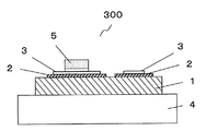
- FIG. 1 is a schematic sectional view showing a power module of the present invention.
- the power module 300 includes a cooler 4, a metal substrate 1, a polyimide resin layer 2, a conductive metal wiring layer 3, and a power semiconductor element 5.
- the power semiconductor element 5 is a semiconductor that controls or supplies power and power, and has a high voltage and large current capacity (output capacity of 100 VA or more and 100 MVA or less) as compared with a normal semiconductor element.
- An element adapted to the operation of the above can be used. Examples thereof include a Schottky barrier diode, a fast recovery diode, a thyristor, a bipolar transistor, a MOSFET, and an IGBT.
- a semiconductor integrated circuit that outputs a desired function in response to a signal from the conductive metal wiring layer 3 is incorporated.
- a control circuit for controlling the output of the power semiconductor element 5 is incorporated in the conductive metal wiring layer 3.
- the power semiconductor element is a wire made of copper, nickel, gold or the like, one end of which is connected to the terminal part, and the other end is wire-bonded to the power semiconductor element (not shown).
- the metal substrate 1 is formed of a material such as a metal having excellent thermal conductivity in order to discharge heat generated from the power semiconductor element 5 mounted via the polyimide resin layer 2.
- the polyimide resin layer 2 is formed in a pattern on the metal substrate 1.
- the cooler 4 the metal substrate 1, the polyimide resin layer 2, the conductive metal wiring layer 3, and the power semiconductor element 5 are sequentially stacked, and the cooler 4 and the metal substrate 1 are sequentially arranged.
- a structure having a stacked region is obtained.
- the polyimide resin layer 2 is an area interposed between the metal substrate 1 and the power semiconductor element 5, and electrically insulates the metal substrate 1 from the power semiconductor element 5 and the conductive metal wiring layer 3. And has a heat conduction function for heat dissipation.
- the metal substrate 1 is made of a material such as a metal having excellent thermal conductivity in order to discharge heat generated from the mounted power semiconductor element 5.
- the polyimide resin layer 2 is formed in a pattern, the metal substrate 1 is exposed in a region where the cooler 4 and the metal substrate 1 of the power module 300 are sequentially laminated, and the heat dissipation effect is great.
- the cooler 4 is fixed and installed with heat conductive grease, a heat radiating adhesive sheet, screws or the like in order to efficiently dissipate heat from the heat source so as to contact the metal substrate 1. It is a component that dissipates the heat to the outside, and is formed of a material with high thermal conductivity such as copper or aluminum and a structure with good cooling properties.
- the heat generated in the power semiconductor element 5 can be easily conducted from the polyimide resin layer 2 to the cooler 4 through the metal substrate 1 and radiated. It becomes possible.
- FIG. 2 is a schematic cross-sectional view showing another embodiment of the power module of the present invention.
- the power module 300 ′ includes a power semiconductor element 5, a conductive metal wiring layer 3, a polyimide resin layer 2, a metal substrate 1, and a cooler 4.
- the polyimide resin layer 2 is formed in a pattern on the metal substrate 1.
- a region where the power semiconductor element 5 is provided on the metal substrate 1 via the polyimide resin layer 2, a cooler 4, the metal substrate 1, and a conductive metal wiring layer are sequentially laminated. And a region in which the cooler 4 and the metal substrate 1 are sequentially laminated.
- the heat generated in the power semiconductor element 5 can be easily conducted to the cooler 4 through the metal substrate 1 and radiated.
- the heat generated from the conductive metal wiring layer can be easily conducted from the polyimide resin layer 2 to the cooler 4 via the metal substrate 1 to be dissipated.
- the metal substrate 1 is exposed and the heat dissipation effect is large.
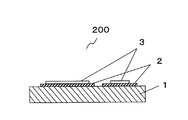
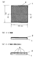
- FIG. 3 is a schematic sectional view showing a substrate 200 with a metal wiring for a power module of the present invention.
- the power module substrate with metal wiring 200 includes a metal substrate 1, a polyimide resin layer 2, and a conductive metal wiring layer 3.
- the polyimide resin layer 2 is formed in a pattern on the metal substrate 1. The function of each layer is the same as described in FIG.
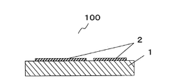
- FIG. 4 is a schematic cross-sectional view showing a power module substrate of the present invention.
- the power module substrate 100 includes a metal substrate 1 and a polyimide resin layer 2.
- the polyimide resin layer 2 is formed in a pattern on the metal substrate 1.
- the metal substrate supports the polyimide resin layer and the conductive metal wiring layer, and has thermal conductivity.
- having thermal conductivity means that the thermal conductivity of the metal substrate at room temperature (300 K) is 10 W / mK or more.
- the metal substrate may be a single layer or a laminate composed of a plurality of layers, but in the case of a laminate, it means that each layer is 10 W / mK or more. Therefore, when the metal substrate is a laminate, the heat conductive adhesive layer or the adhesive sheet, specifically, the copper-heat conductive adhesive layer or the adhesive sheet-aluminum three-layer structure.
- the heat conductive adhesive layer is also included in the metal substrate in the present invention when the heat conductivity is 10 W / mK or more.
- the higher the value of thermal conductivity the better. More specifically, it is more preferably 50 W / mK, particularly preferably 100 W / mK or more, and more preferably 200 W / mK or more. Further preferred.
- the linear thermal expansion coefficient of the metal substrate is preferably in the range of 0 ppm / ° C. to 25 ppm / ° C. from the viewpoint of dimensional stability.
- the said support base material is cut
- the measurement conditions were a heating rate of 10 ° C./min, a tensile load of 1 g / 25,000 ⁇ m 2 so that the weight per cross-sectional area of the evaluation sample was the same, and an average linear thermal expansion within a range of 100 ° C. to 200 ° C.
- the coefficient is the linear thermal expansion coefficient (C.T.E.).
- any thermal conductive material that can stably support the polyimide resin layer and the conductive metal wiring layer and have a desired thermal conductivity can be used. It is not particularly limited, for example, aluminum, aluminum alloy, copper, copper alloy, phosphor bronze, stainless steel (SUS), gold, gold alloy, nickel, nickel alloy, silver, silver alloy, tin, tin alloy, titanium And metal materials such as iron, iron alloy, zinc, molybdenum and invar, and semiconductor materials such as silicon and graphite.
- aluminum, copper, silver, gold and alloys based on these, silicon, or graphite are preferable. This is because the thermal conductivity is high and the heat dissipation is excellent.
- metal material aluminum, copper, and an alloy containing these as main components are preferable.
- aluminum is particularly preferable from the viewpoint of reducing the weight of the metal substrate.
- Copper is preferable when the metal thickness is large and heat dissipation is important.
- process resistance such as chemical resistance and heat resistance.
- the material is a metal material, copper, silver, and gold are preferable. It is because it has high chemical resistance and heat resistance.
- a metal substrate made of a metal having such a large ionization tendency or an alloy containing the metal as a main component is used.
- a protective layer or the like it is preferable to form and use a protective layer or the like. More specifically, when a metal substrate made of aluminum or an alloy containing aluminum as a main component is included, a protective layer formed on the metal substrate is preferably included. This is because the chemical resistance of the polyimide resin layer can be improved during patterning, and it can be prevented from being attacked by an acidic chemical solution or an alkaline chemical solution, particularly an alkaline chemical solution.
- the material constituting the protective layer is not particularly limited as long as it has a desired chemical resistance, and examples thereof include an alkali-resistant material having a desired alkali resistance, mainly composed of an inorganic material. Can be mentioned.
- the formation location is not particularly limited as long as it is formed so as to cover at least a part of the surface of the metal substrate to be protected, but the polyimide resin layer of the metal substrate is formed in plan view. Of the surface on the side to be formed, it is preferable to include all of the region where the metal substrate is exposed when the polyimide resin layer is patterned. More preferably, the entire surface is preferable, and the entire surface of the metal substrate is more preferable. This is because, when the formation location is the above-described region, it is possible to effectively suppress erosion caused by an alkali developer and an etching solution used when patterning the polyimide resin layer.
- the metal substrate is a laminate and has an adhesive layer that improves the adhesion with the polyimide resin layer on the polyimide resin layer side surface
- it is not particularly limited as long as it has a thermal conductivity of 5 and can improve the adhesion to the polyimide resin layer, and can be made of the above-mentioned thermally conductive material.
- the thickness can be in the range of 1 nm to 1000 nm, for example.
- the value of the thermal conductivity of the adhesive layer is relatively smaller than the material mainly constituting the metal substrate, it is preferably 1 nm to 500 nm, preferably 1 nm to 100 nm. More preferably. If it is more than that, the process takes time and costs become high.
- the shape of the metal substrate is not particularly limited, and even if the shape is a flat shape and controlled by a surface roughness with a nanometer order period, the cross-sectional shape of the metal substrate is in contact with the cooler.
- corrugation in a surface or a contact surface with a polyimide-type resin layer may be sufficient.
- the surface area increases.
- the adhesion is good, the thermal diffusion is good, and the heat dissipation can be improved.
- the surface area is increased, and the adhesion is improved by the anchor effect. Further, the exposed portion of the metal surface on which the polyimide resin layer is patterned has increased adhesion with the sealing material due to anchor curing with the sealing resin, thereby improving reliability.
- the height of the irregularities is preferably 0.2 ⁇ m or less because the filler component is clogged, that is, there is a risk of reducing the insulation.
- a method for forming irregularities for example, a method of directly embossing, etching, sandblasting, frosting, stamping, etc.
- a method of forming an irregular pattern using a photoresist, etc., plating A method is mentioned.
- embossing for example, a rolling roll having irregularities on the surface may be used.
- etching processing a chemical is selected according to the type of metal substrate.
- embossing and etching are preferably used from the viewpoint of cost.
- the unevenness width, pitch, and the like are appropriately selected according to the type of metal substrate, the application of the present invention, and the like, and a range suitable for heat conduction can be obtained by simulation, for example.
- the thickness of the metal substrate is not particularly limited as long as it has thermal conductivity, and is appropriately selected according to the use of the power module.
- the thicker the metal substrate the better the thermal diffusion in the surface direction. That is, by making the heat capacity of the metal substrate large, it becomes possible to easily diffuse the local heat at the part in contact with the element, lower the maximum temperature of the part, and prevent damage to the element. As a result, heat dissipation can be improved.
- the present invention when it is used for a power semiconductor element having a large calorific value, it may be anything that can exhibit particularly excellent heat dissipation, and specifically, it may be 1 mm to 5 mm. preferable. This is because when the thickness is in the above-described range, excellent heat dissipation can be achieved.
- the metal substrate may have a protective layer for improving adhesion with the polyimide resin layer, preventing rust, and chemical resistance.
- the soot protective layer is effective in protecting the chemical solution during the manufacturing process, protecting the chemical solution that may ooze out from the module sealing resin from acid and base, and improving the adhesion to the polyimide resin layer.
- the method for forming the protective layer is not particularly limited as long as it is a method that can be stably formed on the surface of the supporting substrate, but rust preventive treatment, plating treatment, anodizing (alumite) treatment, Alternatively, a method using chemical conversion treatment, that is, the metal substrate protective layer is preferably an oxide layer formed by anodizing treatment, an oxide layer or sulfide layer formed by chemical conversion treatment, or a plating layer.
- the thickness is preferably 1 ⁇ m or more. Among them, the thickness is preferably 5 ⁇ m or more, and particularly preferably 10 ⁇ m or more.
- the polyimide resin layer patterning method forms a resist pattern on the polyimide film obtained by imidizing the polyimide resin precursor.
- the metal substrate can be stably protected even with an extremely strong alkaline solution such as an etching solution or a resist stripping solution used in the case of patterning by etching and then stripping the resist.
- the protective layer may be subjected to a surface treatment such as unevenness like the metal substrate. Or you may make it follow the unevenness
- about an upper limit since it is preferable from the viewpoint that alkali resistance can be improved, so that it is thick, there is no particular limitation. However, since the cost increases as the thickness increases, it is usually set to 100 ⁇ m or less.
- a plating method As a plating method, a commonly used plating method can be used. Specifically, a wet plating method (electrolytic plating method or electroless plating method), a dry plating method (vacuum deposition method, sputtering method, metallicon method). ) Etc. can be used. Among them, the wet plating method is preferable, and the electrolytic plating method is particularly preferable. This is because a denser plating layer can be formed. Further, as a result, even when the thickness is thin, the alkali resistance can be sufficiently improved. Moreover, in the wet plating, the plating speed is fast, so that the plating time can be shortened.
- Electroplating used as a wet plating method is a method in which a substance (metal) is electrically connected to the surface of a conductive object by passing a direct current through an electrolytic solution containing the substance to be plated, using the conductive object as a cathode. Etc.) is reduced and deposited to form a layer.
- the metal in the case of performing electroplating is not particularly limited as long as it is a metal with higher chemical resistance than the metal substrate to be protected and has high adhesion to the polyimide resin layer, manganese, zinc, chromium, iron, Examples thereof include cadmium, cobalt, nickel, tin, lead, bismuth, copper, silver, palladium, iridium, platinum, gold, gallium, ruthenium, rhodium, indium, and osmium.
- nickel plating since nickel plating has a dense surface, it is preferable from the viewpoint of preventing rust, improving the adhesion to the polyimide resin layer, and cost.
- the substance in the solution containing the substance to be plated, the substance (on the surface of the object to be plated (electrically) by the electrons released by the oxidation of the reducing agent contained in the solution, not the electrons caused by energization. A metal or the like) is reduced and deposited to form a layer.
- the electroless plating method has the advantage that the film thickness unevenness can be reduced, and since the conductivity is not required for the object to be plated at the time of plating, the object for forming the metal substrate protective layer is made of aluminum or aluminum. Even if it is a metal base material which consists of an alloy which has a main component, it has the advantage that it can be set as a thing with few plating irregularities.
- the metal in the case of performing electroless plating is not particularly limited as long as it is a metal having higher chemical resistance than the metal substrate to be protected, and is not limited to cadmium, cobalt, nickel, tin, lead, bismuth, copper, silver, Examples include palladium, platinum, gold, ruthenium, rhodium, and indium.
- Dry plating is a method in which a metal, oxide, nitride, or the like is gasified, ionized, or liquefied and then deposited on the surface of the material.
- the metal for dry plating is not particularly limited as long as it is a metal with higher chemical resistance than the metal substrate to be protected.
- the metal base is made of aluminum or an alloy containing aluminum as a main component.
- the dry plating method not only metals but also metals and non-metal oxides and nitrides can be stacked.
- oxides of metals such as Cr, Zn, In, Ga, Cd, Ti, Sn, Te, Mg, W, Mo, Cu, Al, Fe, Sr, Ni, Ir, Mg, Si,
- a film made of a non-metallic oxide such as Ge or B, or a nitride, sulfide, selenide, or mixture of the above elements can be formed.
- a conductive object is used as an anode in an electrolytic solution, and a direct current is passed to electrically oxidize the conductive object to form an oxide layer (oxide film layer) on the surface. It is to be formed.
- the electrolytic solution in the case of anodizing is not particularly limited as long as it can form an oxide film having a sufficient thickness on the metal substrate to be protected, a sulfuric acid bath, an oxalic acid bath, a chromic acid bath, An acidic bath such as a phosphoric acid bath, an alkaline bath such as a sodium hydroxide bath and an ammonia bath can be used.
- Chemical conversion treatment uses a chemical reaction such as oxidation or sulfidization in solution to chemically react with the surface of the support substrate to form a corrosion-resistant film such as an oxide layer (oxide film) or sulfide layer (sulfide film). It is a method to do.
- a corrosion-resistant film such as an oxide layer (oxide film) or sulfide layer (sulfide film).
- Such chemical conversion treatment has an advantage that the corrosion-resistant film can be easily formed on the entire surface (including the end surface) because it can be formed without connecting the electrodes.
- the solution for the chemical conversion treatment is not particularly limited as long as it can form a corrosion-resistant film having a sufficient thickness on the supporting base material to be protected. Phosphoric acid / chromate, chromate Type, alkali / chromate type, boehmite type, zirconium type, zinc phosphate type and the like.
- the material constituting the metal substrate is a metal material because the processing is easy in a photolithography method, a method of directly processing by laser, punching, or the like. It is because the metal substrate having the metal substrate protective layer can be easily formed by forming the metal substrate protective layer by such a method.
- the conductive metal wiring layer used in the present invention is formed directly on the polyimide resin layer, and can be electrically connected to the power semiconductor element disposed on the power module substrate of the present invention. Usually, it includes a conductive layer made of a conductive material. In the present invention, the conductive metal wiring layer is used as appropriate before and after pattern formation.
- the material used for the conductive metal wiring layer is not particularly limited as long as it is a conductive material, and is appropriately selected depending on the presence or absence of transparency.
- a conductive material For example, Al, Au, Ta, W, Pt, Ni, Pd, Cr, Cu, Mo, simple metals such as alkali metals and alkaline earth metals, oxides of these metals, Al alloys such as AlLi, AlCa and AlMg, Mg alloys such as MgAg, Ni alloys , Cr alloys, alkali metal alloys, alkaline earth metal alloys, and the like.
- These conductive materials may be used alone, in combination of two or more kinds, or may be laminated using two or more kinds.
- conductive oxides such as indium tin oxide (ITO), indium zinc oxide (IZO), tin oxide, zinc oxide, indium oxide, and aluminum zinc oxide (AZO) can also be used.
- the electrical resistivity is preferably 1.0 ⁇ 10 ⁇ 6 ⁇ ⁇ m or less, more preferably 1.0 ⁇ 10 ⁇ 7 ⁇ ⁇ m or less, More preferably, it is 3.0 ⁇ 10 ⁇ 8 ⁇ ⁇ m. This is because in the case of flowing a large current, the effect of suppressing the loss becomes remarkable, and heat generation can be reduced.
- the thickness of the conductive metal wiring layer is appropriately set according to the use of the substrate with metal wiring for power module of the present invention.
- 100 ⁇ m to 500 ⁇ m is preferable from the viewpoint of preventing short circuit due to heat generation and easy heat dissipation from the conductive metal wiring layer.
- 100 ⁇ m is preferable.
- ⁇ 300 ⁇ m is preferred.
- the conductive metal wiring layer includes a conductive layer made of the conductive material. If necessary, the conductive metal wiring layer has an adhesion layer for improving the adhesion to the polyimide resin layer on the polyimide resin layer side surface, and an electron. It may have a protective layer such as a plating layer for preventing oxidative deterioration of the conductive metal wiring layer on the surface where the element is disposed.
- the adhesion layer is not particularly limited as long as the adhesion between the polyimide resin layer and the conductive metal wiring layer can be improved, but the adhesion layer used for the support substrate is not limited. Can be similar.
- examples of the plating layer include tin, nickel, silver, and gold plating layers. Further, a nickel plating layer may be formed as a base for the gold plating layer. The thickness of the plating layer can be in the range of 0.01 ⁇ m to 4.0 ⁇ m, for example.
- the method for forming the conductive metal wiring layer is not particularly limited as long as the conductive metal wiring layer is formed directly on the polyimide resin layer.
- the method and conditions for providing a metal layer by the metallization method on the polyimide resin layer are not particularly limited, and any method of thermocompression bonding, vapor deposition, sputtering, and plating may be used. Further, a method of combining a plurality of these methods may be used. Specifically, when the adhesive layer is included, first, an adhesive layer made of an inorganic material is formed on the polyimide resin layer by sputtering or the like, and then the conductive layer is formed by vapor deposition or plating. A method of forming a layer can be used.
- the surface of the conductive metal wiring layer may be roughened or roughened, and chemical processing, plasma processing, embossing, etching, sandblasting, frosting, stamping, etc.
- embossing for example, a rolling roll having irregularities on the surface may be used.
- etching processing a chemical is selected according to the type of metal substrate. Note that the unevenness width, pitch, and the like are appropriately selected according to the type of metal substrate, the application of the present invention, and the like, and a range suitable for heat conduction can be obtained by simulation, for example.
- a general method can be used. For example, a method of depositing the conductive material through a mask, or forming the conductive metal wiring layer. Then, a method of etching using a resist can be used.
- a method of depositing the conductive material through a mask, or forming the conductive metal wiring layer. Then, a method of etching using a resist can be used.
- the polyimide resin layer of the present invention is configured to include at least one thermoplastic polyimide resin layer.
- the polyimide resin layer preferably includes a non-thermoplastic polyimide resin layer in addition to the thermoplastic polyimide resin layer.
- the order is determined in consideration of the above physical properties of the thermoplastic polyimide resin layer and the non-thermoplastic polyimide resin layer.
- the non-thermoplastic polyimide resin layer is first formed of the conductive metal layer for the metal substrate or conductive metal wiring layer. It is formed on the surface of the conductive metal layer for the metal substrate or the conductive metal wiring layer after the layer containing the thermoplastic resin is formed on the surface by the direct coating method, etc. Are preferably formed.
- thermoplastic polyimide resin layer is first formed on a metal substrate and a conductive metal layer, and a layer containing a non-thermoplastic insulating resin is used as an intermediate layer. After being formed and finally forming a layer containing a thermoplastic resin, it is formed by being in close contact with the surface of the conductive metal layer for the metal substrate or the conductive metal wiring layer and bonded by a heating and pressing method.
- substrate with a metal wiring for modules excellent in insulation and adhesiveness is obtained.
- the conductive metal wiring layer or metal substrate and the polyimide precursor chemically interact to contact each other at the interface.
- heat transfer is improved and heat dissipation is improved, and the heat dissipation and heat resistance of the power module is achieved by constructing a material that has a small difference between the linear thermal expansion and the conductive metal wiring layer and metal substrate.
- substrate with a metal wiring for power modules which eliminates the restriction
- Chemical interaction refers to the interaction with the surface of the conductive metal wiring layer or metal substrate without providing an adhesive layer.
- the hydroxyl group, carbonyl group, or amino group in the polyimide precursor is the conductive metal wiring layer. It interacts electrically with the surface of the metal substrate and increases the adhesion to the conductive metal wiring layer and the surface of the metal substrate even after heat curing, and eliminates contact resistance and improves heat dissipation. .
- thermoplastic polyimide resin that can be thermocompression bonded, and adheres well to metal substrates or conductive metal wiring layers by heating and pressurizing, so there is no deterioration in insulation due to peeling or cracking, and heat dissipation. Good effect can be obtained.
- the thermoplastic polyimide resin layer is 4 times thinner than the non-thermoplastic polyimide resin layer, which adversely affects the film thickness change due to linear thermal expansion and softening, dimensional change of the conductive metal wiring layer, and insulation. It is hard to affect.
- the non-thermoplastic polyimide resin layer has a small linear expansion due to the linear expansion of the metal substrate and the conductive metal wiring layer. As a result, the effect of improving the reliability can be obtained.
- the glass transition temperature (Tg) of the polyimide resin layer as a whole is preferably 260 ° C. or higher, and particularly preferably 270 ° C. or higher from the viewpoint of heat resistance. It is because the heat resistance of the module substrate of the present invention can be made sufficiently high when the Tg is within the above range. The higher the Tg, the better the heat resistance, but it is usually preferable to cure (heat treatment) at a temperature higher than the Tg in order to bring out the physical properties of the polyimide. There is a possibility that the resin layer and the metal substrate deteriorate. From such a viewpoint, the upper limit of Tg is preferably 500 ° C. or lower.
- the temperature at which the polyimide resin layer begins to soften is around 250 ° C. or lower, and it is in an environment such as an engine room or around an element with a high temperature process such as solder reflow or a high temperature at start-up. This is because the polyimide resin layer may begin to soften, and accordingly, insulation, heat dissipation, and adhesion may be deteriorated. Conversely, when Tg is higher than the above range, the temperature at which softening starts is high, so that the thermal stress cannot be sufficiently relaxed, or the polyimide resin layer, the metal substrate, etc. may be deteriorated. .
- the polyimide resin layer preferably has no melting point at 260 ° C. or lower, more preferably has no melting point at 270 ° C. or lower, and more preferably has no melting point at 300 ° C. or lower. It is because the heat resistance of the board with metal wiring for modules of the present invention can be made sufficiently high.
- the total thickness of the polyimide resin layer 2 is in the range of 20 ⁇ m to 150 ⁇ m, exhibits desired insulation, prevents short circuit between the metal substrate and the conductive metal wiring layer, and exhibits desired heat dissipation.
- the voltage it is not particularly limited, and is set according to the required withstand voltage.
- the voltage used is less than 4 k, it is 20 ⁇ m to 70 ⁇ m, more preferably 20 ⁇ m to 50 ⁇ m from the viewpoint of heat dissipation. In the case of about 4 kV, it is preferably 20 ⁇ m to 100 ⁇ m, and preferably 20 ⁇ m to 70 ⁇ m from the viewpoint of heat dissipation.
- the voltage used is about 6 kV, it is preferably 20 ⁇ m to 150 ⁇ m, preferably 20 ⁇ m to 100 ⁇ m from the viewpoint of heat dissipation and peeling. If it is more than 10 kV, 40 ⁇ m to 150 ⁇ m is preferable from the viewpoint of withstand voltage. Further, the thermal conductivity at this time is preferably 1 W / mK to 13 W / mK, and preferably 2.5 W / mK to 13 W / mK from the viewpoint of thinning and heat dissipation.
- a film having only the polyimide resin layer is prepared for measurement of thermal conductivity.
- a method of peeling the insulating laminate, or after producing a polyimide resin layer on a metal plate the metal plate is removed by etching, and a polyimide resin layer There is a method of obtaining the film.
- the obtained film of the polyimide resin layer is cut into a width of 30 mm and a length of 30 mm to obtain an evaluation sample.
- a blackening material carbon spray
- the thermal conductivity ⁇ is the specific heat Cp, the thermal diffusivity ⁇ , and the density ⁇ of the test piece.
- the product ⁇ ⁇ ⁇ Cp ⁇ ⁇ was obtained.
- the linear thermal expansion coefficient of the polyimide-based resin layer 2 is within the range of 0 ppm / ° C. to 40 ppm / ° C. from the viewpoint of heat dissipation and insulation due to peeling and cracking when using the power wiring board for power modules of the present invention. Preferably there is. This is because if the linear thermal expansion coefficient is too large, the expansion and contraction that occurs when the temperature changes is increased, which adversely affects the above viewpoint. Moreover, even if it is a case where what consists of metal materials excellent in heat dissipation, such as copper and aluminum, is used as said metal substrate, generation
- the difference between the linear thermal expansion coefficient of the polyimide resin layer 2 and the linear thermal expansion coefficient of the metal substrate 1 and the conductive metal wiring layer 3 is preferably 15 ppm / ° C. or less from the viewpoint of peeling and cracking. More preferably, it is 10 ppm / ° C. or less, and further preferably 5 ppm / ° C. or less.
- the substrate with metal wiring for power module 200 is preferably not peeled in a temperature environment in the range of 0 ° C. to 100 ° C., preferably 0 ° C. to 150 ° C., 0 ° C. to 260 ° C. If the difference in linear thermal expansion coefficient between the polyimide resin layer 2 and the metal substrate 1 is greatly different because the polyimide resin layer 2 has a large linear thermal expansion coefficient, the power module substrate with metal wiring 200 changes in the thermal environment. Will peel off.
- the linear thermal expansion coefficient is measured as follows. First, a film having only the polyimide resin layer is prepared. After producing a film consisting only of a polyimide resin layer on a metal plate, after removing the insulating laminate, or after producing a polyimide resin layer on a metal plate, the metal plate is removed by etching. There is a method of obtaining a resin layer film. Next, the obtained polyimide resin layer film is cut into a width of 5 mm and a length of 20 mm to obtain an evaluation sample. The linear thermal expansion coefficient is measured by a thermomechanical analyzer (for example, Thermo Plus TMA8310 manufactured by Rigaku Corporation).
- a thermomechanical analyzer for example, Thermo Plus TMA8310 manufactured by Rigaku Corporation.
- the measurement conditions were a heating rate of 10 ° C./min, a tensile load of 1 g / 25,000 ⁇ m 2 so that the weight per cross-sectional area of the evaluation sample was the same, and an average linear thermal expansion within a range of 100 ° C. to 200 ° C.
- the coefficient is the linear thermal expansion coefficient (C.T.E.).
- the water absorption of the polyimide-based resin layer 2 is preferably relatively small because it can be considered to be a water-based process or a long-term storage in terms of operation and process in a high-humidity environment.
- One index of water absorption is the hygroscopic expansion coefficient. Therefore, it is preferable that the hygroscopic expansion coefficient of the polyimide resin layer 2 is as small as possible. Specifically, it is preferably in the range of 0 ppm /% RH to 15 ppm /% RH, more preferably 0 ppm /% RH to 12 ppm. /% RH, more preferably 0 ppm /% RH to 10 ppm /% RH.
- the hygroscopic expansion coefficient of the polyimide resin layer 2 is in the above range, the water absorption of the polyimide resin layer 2 can be sufficiently reduced, and the substrate with metal wiring for power module of the present invention can be easily stored. This is because when the element is manufactured using the substrate with metal wiring for power module, the process becomes simple.
- the smaller the hygroscopic expansion coefficient of the non-thermoplastic polyimide the lower the concern about peeling and cracking of the polyimide resin layer 2.
- the hygroscopic expansion coefficient of the polyimide-based resin layer 2 is large, due to the difference in expansion coefficient from the metal substrate whose hygroscopic expansion coefficient is almost zero, the adhesiveness with the metal substrate and wiring decreases with increasing humidity. Because there are cases.
- a measuring method of a hygroscopic expansion coefficient it can measure with a humidity variable mechanical analyzer (Thermo Plus TMA8310 by Rigaku).
- the tensile weight is set to 1 g / 25000 ⁇ m 2 so that the weight per cross-sectional area of the evaluation sample becomes the same.
- the glass transition temperature (Tg) of the polyimide resin constituting the polyimide resin layer 2 is preferably 260 ° C. or higher, and particularly preferably 270 ° C. or higher from the viewpoint of heat resistance. It is because the heat resistance of the board with a metal wiring for a power module of the present invention can be made sufficiently high when the Tg is within the above range.
- Tg is higher than the above range, the temperature at which softening begins is high, so the thermal stress cannot be sufficiently relaxed, or the polyimide resin layer 2 and the metal substrate 1 may be deteriorated.
- the polyimide resin layer 2 does not have a melting point at 260 ° C. or less, more preferably it does not have a melting point at 270 ° C. or less, and further preferably does not have a melting point at 300 ° C. or less. .
- the heat resistance of the power wiring board for power module of the present invention can be made sufficiently high.
- Thermoplastic polyimide resin layer Specifically, as the thermoplastic polyimide resin constituting the polyimide resin layer 2, the storage elastic modulus in the temperature range from room temperature (about 25 ° C.) to 300 ° C. or the glass transition temperature + 20 ° C., whichever is lower. Is a polyimide resin that is always less than 1.0 ⁇ 10 8 Pa.
- the storage elastic modulus in the temperature range from room temperature (about 25 ° C.) to 300 ° C. or the glass transition temperature + 20 ° C., whichever is lower, is particularly limited as long as it is always less than 1.0 ⁇ 10 8 Pa.
- the thermoplastic polyimide resin is in the range of 9.0 ⁇ 10 7 Pa to 1.0 ⁇ 10 5 Pa, and more preferably 5.0 ⁇ 10 7 Pa to 1. It is preferably within the range of 0 ⁇ 10 5 Pa.
- the metal substrate 1 or the conductive metal wiring layer 3 is difficult to stick by thermocompression bonding, and a gap is generated between the polyimide resin layer and peeling during a long-term operation. Occurs and leads to deterioration of reliability.
- a polyimide resin layer having a storage elastic modulus of 1.0 ⁇ 10 8 Pa or more is always used in a temperature range from room temperature (about 25 ° C.) to 300 ° C. or a glass transition temperature + 20 ° C., whichever is lower.
- the polyimide resin layer of less than 1.0 ⁇ 10 8 Pa is laminated on the surface that is in contact with the metal substrate 1 or the conductive metal wiring layer 3 or the surface of the metal layer that is necessarily thermocompression bonded.
- the thickness of the polyimide resin layer of less than 1.0 ⁇ 10 8 Pa to be laminated is not particularly specified, but is preferably 25% or less of the polyimide resin layer of 1.0 ⁇ 10 8 Pa or more from the viewpoint of the thermal expansion coefficient. .
- the storage elastic modulus is a value measured using a dynamic viscoelasticity measuring device (for example, RSA3 manufactured by TA Instruments) under the conditions of a frequency of 1 Hz and a heating rate of 5 ° C./min.
- a dynamic viscoelasticity measuring device for example, RSA3 manufactured by TA Instruments
- the polyimide resin is aromatic from the viewpoint of making the heat resistance, linear thermal expansion coefficient, hygroscopic expansion coefficient, thermal conductivity, and storage elastic modulus of the polyimide resin layer 2 suitable for the power module substrate of the present invention.
- a polyimide resin containing a skeleton is preferable.
- polyimide resins polyimide resins containing aromatic skeletons are derived from their rigid and highly planar skeletons, which have excellent heat resistance and insulation properties in thin films, high thermal conductivity, and linear thermal expansion. It is because it is preferably used for the polyimide resin layer 2 of the power module substrate with metal wiring 200 because the coefficient is low.
- R 1 is a tetravalent organic group
- R 2 is a divalent organic group
- R 1 and R 2 that are repeated may be the same or different from each other.
- n is a natural number of 1 or more.
- R 1 is a structure derived from tetracarboxylic dianhydride
- R 2 is a structure derived from diamine
- a polyimide resin is composed of tetracarboxylic dianhydride and It is obtained by reacting diamine to synthesize a polyimide resin precursor such as polyamic acid and then imidizing it thermally or chemically. That is, the polyimide resin precursor is a compound in the previous stage where the polyimide resin is produced.
- the tetracarboxylic dianhydride preferably used from the viewpoints of the heat resistance and linear thermal expansion coefficient of the polyimide resin is an aromatic tetracarboxylic dianhydride.
- Particularly preferred tetracarboxylic dianhydrides include pyromellitic dianhydride, merophanic dianhydride, 3,3 ′, 4,4′-benzophenone tetracarboxylic dianhydride, 3,3 ′, 4.
- 3,3 ′, 4,4′-biphenyltetracarboxylic dianhydride, 2,3,3 ′, 4′-biphenyltetracarboxylic dianhydride, 2,3 2,2 ′, 3′-biphenyltetracarboxylic dianhydride and bis (3,4-dicarboxyphenyl) ether dianhydride are particularly preferred.
- the tetracarboxylic dianhydride into which fluorine is introduced is used as the tetracarboxylic dianhydride used in combination, the hygroscopic expansion coefficient of the polyimide resin is lowered.
- a polyimide resin precursor having a fluorine-containing skeleton is difficult to dissolve in a basic aqueous solution and needs to be developed with a mixed solution of an organic solvent such as alcohol and a basic aqueous solution.
- pyromellitic dianhydride merophanic dianhydride, 3,3 ′, 4,4′-biphenyltetracarboxylic dianhydride, 2,3,3 ′, 4′-biphenyltetracarboxylic dianhydride
- rigid tetracarboxylic dianhydrides such as 2,3,2 ′, 3′-biphenyltetracarboxylic dianhydride and 1,4,5,8-naphthalenetetracarboxylic dianhydride are used, Since the linear thermal expansion coefficient of resin becomes small, it is preferable.
- the polyimide resin contains any structure of the above formula, it is derived from these rigid skeletons and exhibits low linear thermal expansion and low hygroscopic expansion. There is also an advantage that it is easily available on the market and is low in cost.
- the polyimide resin having the structure as described above is a polyimide resin exhibiting high heat resistance and a low linear thermal expansion coefficient. Therefore, the content of the structure represented by the above formula is preferably closer to 100 mol% of R 1 in the formula (I), but at least 33 mol% or more of R 1 in the formula (I). It may be contained. Among them, the content of the structure represented by the above formula is preferably 50 mol% or more, more preferably 70 mol% or more, of R 1 in the formula (I).
- the benzene rings interact with each other to form a core and improve thermal conductivity.
- the skeleton does not become a rigid skeleton, and the linear thermal expansion coefficient and humidity expansion coefficient may decrease.
- the polyimide resin having the structure as described above is a polyimide resin showing an improvement in thermal conductivity. Therefore, the content of the structure represented by the above formula may be at least 33 mol% or more of R 1 in the above formula (I). Further, in this case, it is used in combination with a tetracarboxylic acid having a rigid skeleton so that the glass transition temperature does not become 260 ° C. or lower.
- the polyimide resin having the above structure in combination with pyromellitic dianhydride, good etching properties can be obtained with respect to an alkaline etching solution of polyimide.
- the amount of pyromellitic dianhydride is 50 mol% to 90 mol% with respect to the acid dianhydride used in combination. From the viewpoint of suppressing humidity expansion, when the tetracarboxylic dianhydride has an alicyclic skeleton, the transparency of the polyimide resin precursor is improved, so that a highly sensitive photosensitive polyimide resin can be obtained.
- the polyimide resin is used in combination with a tetracarboxylic acid having an aromatic skeleton of 33 mol% or more.
- a diamine component applicable to the polyimide resin one kind of diamine can be used alone, or two or more kinds of diamines can be used in combination.
- the diamine component used is not particularly limited. For example, p-phenylenediamine, m-phenylenediamine, o-phenylenediamine, 3,3′-diaminodiphenyl ether, 3,4′-diaminodiphenyl ether, 4,4 ′.
- a diamine or the like obtained by substituting a part or all of the hydrogen atoms on the aromatic ring of the diamine with a substituent selected from a fluoro group, a methyl group, a methoxy group, a trifluoromethyl group, or a trifluoromethoxy group. Can do.
- the polyimide resin in order to make the polyimide resin have a storage elastic modulus that expresses a desired thermoplasticity, two or more kinds of diamines as raw materials constituting the polyimide resin contained as a main component are mixed.
- the one or more diamines preferably contain a flexural raw material ratio of 50 mol% or more, and may be block copolymerization or random polymerization.
- random polymerization in which amines are randomly arranged is storage elastic modulus. From the viewpoint of.
- the amino group is preferably meta-coordinated from the viewpoint of lowering the storage elastic modulus and improving the adhesion, and n is preferably 1 to 3 from the viewpoint of heat resistance.
- the diamine component to be used is not particularly limited.
- DANPG 1,3-bis (4-aminophenoxy) -2,2-dimethylpropane
- BAPP 2,2-bis [4- (4-aminophenoxy) phenyl] propane
- APB 3-bis (3-aminophenoxy) benzene
- p-PDA paraphenylenediamine
- DPE 3,4'-diaminodiphenyl ether
- ODA 4,4'-diaminodiphenyl ether
- the diamine can be selected depending on the desired physical properties. If a rigid diamine such as p-phenylenediamine is used, the polyimide resin has a low expansion coefficient.
- rigid diamines include p-phenylenediamine, m-phenylenediamine, 1,4-diaminonaphthalene, 1,5-diaminonaphthalene, 2,6 as diamines in which two amino groups are bonded to the same aromatic ring. -Diaminonaphthalene, 2,7-diaminonaphthalene, 1,4-diaminoanthracene and the like.
- diamines in which two or more aromatic rings are bonded by a single bond, and two or more amino groups are each bonded directly or as part of a substituent on a separate aromatic ring for example, Some are represented by the following formula (II). Specific examples include benzidine and the like.
- a is a natural number of 0 or 1 or more, and the amino group is bonded to the meta position or the para position with respect to the bond between the benzene rings.
- a diamine having a substituent at a position where the amino group on the benzene ring is not substituted without being involved in the bond with other benzene rings can also be used. These substituents are monovalent organic groups, but they may be bonded to each other.
- R 3 is a divalent organic group, an oxygen atom, a sulfur atom, or a sulfone group, and R 4 and R 5 are a monovalent organic group or a halogen atom.
- the polyimide resin contains any structure of the above formula, it is derived from these rigid skeletons and exhibits low linear thermal expansion and low hygroscopic expansion. Furthermore, there is also an advantage that it is easily available on the market and is low cost.
- p-phenylenediamine, m-phenylenediamine, 1,4-diaminonaphthalene, etc. are rigid diamines such as p-phenylenediamine in which two amino groups are bonded to the same aromatic ring. 1,5-diaminonaphthalene, 2,6-diaminonaphthalene, 2,7-diaminonaphthalene, 1,4-diaminoanthracene and the like.
- R 3 in [Chemical Formula 4] is a divalent organic group, an oxygen atom, a sulfur atom, or a sulfone group
- R 4 and R 5 are a monovalent organic group or a halogen atom.
- the compound of [Chemical Formula 4] and diamines in which one benzene ring is inserted with a divalent organic group, oxygen atom, sulfur atom, or sulfone group between two benzene rings having an amino group are also included.
- the content of the structure represented by the above formula may be at least 33 mol% or more of R 2 in the above formula (I).
- Diamine compounds such as 4,4′-diamino-2,2′-dimethylbiphenyl and 4,4′-diaminodiphenyl ether have good etchability with an alkaline etchant, and contain 33 mol% or more of paraphenylenediamine, 4,4 ′
- -diamino-2'-methoxybenzanilide or the like it is possible to expect the effect of exhibiting good etching property and low thermal expansion.
- Solvents used in the varnish solution are generally N-methylpyrrolidone (NMP), methylformamide (DMF), dimethylacetamide (DMAc), dimethyl sulfoxide (DMSO), dimethyl sulfate, sulfolane, butyrolactone, Examples include cresol, phenol, halogenated phenol, cyclohexane, dioxane, tetrahydrofuran, diglyme, and triglyme.
- NMP N-methylpyrrolidone
- DMF methylformamide
- DMAc dimethylacetamide
- DMSO dimethyl sulfoxide
- sulfate dimethyl sulfate
- sulfolane butyrolactone
- Examples include cresol, phenol, halogenated phenol, cyclohexane, dioxane, tetrahydrofuran, diglyme, and triglyme.
- the method for forming the non-thermoplastic polyimide resin layer is not particularly limited as long as it can be directly formed on a metal substrate or a conductive metal wiring layer (before wiring formation). Extrusion molding, application, etc.
- a spin coating method for example, a spin coating method, a die coating method, a dip coating method, a bar coating method, a gravure printing method, a screen printing method, or the like can be used.
- Non-thermoplastic polyimide-based resins are those that do not have thermoplasticity, that is, those that do not exhibit plasticity at a temperature at which a general thermoplastic polyimide exhibits thermoplasticity, specifically,
- the storage elastic modulus in the temperature range from room temperature (about 25 ° C.) to 300 ° C. or the glass transition temperature + 20 ° C., whichever is lower, is particularly limited as long as it is always 1.0 ⁇ 10 8 Pa or more. Although not intended, it is preferably within the range of 1.0 ⁇ 10 8 Pa to 1.0 ⁇ 10 11 Pa, and more preferably within the range of 5.0 ⁇ 10 8 Pa to 5.0 ⁇ 10 10 Pa. Preferably there is.
- the polyimide resin layer may begin to soften during high-temperature processes such as solder reflow, so the film thickness changes during heating, the dimensions of the conductive metal wiring layer change, This is because the insulating property may be deteriorated by the change in thickness.
- a polyimide is only a polyimide-type resin layer which has thermoplasticity, it is necessary to use the monomer (mainly diamine) of a flexible frame
- the storage elastic modulus when the storage elastic modulus is higher than the above range, it is difficult to soften the film to a level at which it is easy to relieve thermal stress during baking, which has an adverse effect on the distortion of the polyimide resin layer and the surface flatness. There is a possibility of effect.
- the storage elastic modulus of a polyimide when the storage elastic modulus of a polyimide is a high thing, it is necessary to use the monomer (mainly diamine) of rigid frame
- the linear expansion coefficient becomes too small and it becomes difficult to match the metal layer.
- the storage elastic modulus is a value measured using a dynamic viscoelasticity measuring apparatus (for example, RSA3 manufactured by TA Instruments) under conditions of a frequency of 1 Hz and a heating rate of 5 ° C./min.
- a dynamic viscoelasticity measuring apparatus for example, RSA3 manufactured by TA Instruments
- thermoplastic polyimide resin in the present application is usually less than 1.0 ⁇ 10 8 Pa in storage modulus in a temperature range from room temperature (about 25 ° C.) to 300 ° C. or the glass transition temperature + 20 ° C., whichever is lower. This means a polyimide having a temperature range of
- the glass transition temperature (Tg) of the non-thermoplastic polyimide resin is not particularly limited as long as it can exhibit desired insulation properties, but is preferably 260 ° C. or higher. It is desirable that it is 270 ° C. or higher from the viewpoint of heat resistance. It is because the heat resistance of the power module substrate of the present invention can be made sufficiently high when the Tg is within the above range.
- the resin layer and the metal substrate may be deteriorated.
- the upper limit of Tg is preferably 500 ° C. or lower.
- Tg is lower than the above range, the temperature at which the polyimide resin layer begins to soften is around 250 ° C. or lower, and the polyimide resin layer may begin to soften during high-temperature processes such as solder reflow. This is because there is a possibility that the insulation properties deteriorate due to the change in the film thickness and the dimensional change of the conductive metal wiring layer.
- Tg is higher than the above range, the temperature at which softening begins is high, so the thermal stress cannot be sufficiently relaxed, or the polyimide resin layer, the substrate with metal wiring for power modules, etc. may deteriorate. Because there is.
- the non-thermoplastic polyimide resin in the present invention preferably has no melting point at 260 ° C. or lower, preferably has no melting point at 270 ° C. or lower, and has no melting point at 300 ° C. or lower. More preferably. This is because the heat resistance of the power wiring board for power module of the present invention can be made sufficiently high.
- the thermal conductivity of the non-thermoplastic polyimide resin layer is not particularly limited as long as it can provide desired thermal conductivity.
- the thermal conductivity of the non-thermoplastic polyimide resin layer is preferably 1 W / mK to 15 W / mK. Furthermore, 2.5 W / mK to 15 W / mK is preferable from the viewpoint of thinning and heat dissipation.
- the coefficient of linear thermal expansion of the non-thermoplastic polyimide resin is within the range of 0 ppm / ° C. to 40 ppm / ° C. from the viewpoint of heat dissipation and insulation due to peeling or cracking when using the substrate with metal wiring for power module of the present invention. It is preferable that This is because if the linear thermal expansion coefficient is too large, the expansion and contraction that occurs when the temperature changes is increased, which adversely affects the above viewpoint. Further, even when the metal substrate is made of a metal material excellent in heat dissipation such as copper or aluminum, the occurrence of peeling or warping can be sufficiently suppressed.
- the linear thermal expansion coefficient is measured as follows. First, a film made of only the non-thermoplastic polyimide resin is prepared. After producing a film (polyimide resin layer) consisting only of the non-thermoplastic polyimide resin on the metal, a method of peeling the polyimide resin layer, or producing the non-thermoplastic polyimide film on the metal substrate. Thereafter, there is a method of removing the metal by etching to obtain the non-thermoplastic polyimide resin film. Next, the obtained non-thermoplastic polyimide resin film is cut into a width of 5 mm and a length of 20 mm to obtain an evaluation sample.
- the linear thermal expansion coefficient is measured by a thermomechanical analyzer (for example, Thermo Plus TMA8310 (manufactured by Rigaku Corporation)).
- the measurement conditions were a heating rate of 10 ° C./min, a tensile load of 1 g / 25,000 ⁇ m 2 so that the weight per cross-sectional area of the evaluation sample was the same, and an average linear heat within a range of 100 ° C. to 200 ° C.
- the expansion coefficient be the linear thermal expansion coefficient (C.T.E.).
- the difference between the coefficient of linear thermal expansion of the non-thermoplastic polyimide resin and the coefficient of linear thermal expansion of the metal is 15 ppm / ° C. or less from the viewpoint of not adversely affecting heat dissipation and insulation due to peeling or cracking. Is preferable, more preferably 10 ppm / ° C. or less, and further preferably 5 ppm / ° C. or less.
- peeling and cracking of the power module metal wiring substrate of the present invention are suppressed, and when the thermal environment of the power module metal wiring substrate is changed, This is because the stress at the interface with the metal substrate is reduced and the adhesion is improved.
- the substrate with metal wiring for power module of the present invention is not peeled off in the temperature environment of 0 ° C. to 100 ° C., preferably 0 ° C. to 150 ° C., 0 ° C. to 260 ° C. in handling.
- the power wiring substrate for the power module will change in the thermal environment. It will peel off due to the difference in expansion coefficient.
- the water absorption of the non-thermoplastic polyimide resin is preferably relatively small because it can be considered to be an aqueous process or long-term storage in terms of operation and process in a high humidity environment.
- One index of water absorption is the hygroscopic expansion coefficient. Therefore, the moisture absorption expansion coefficient of the non-thermoplastic polyimide resin is preferably as small as possible. Specifically, it is preferably in the range of 0 ppm /% RH to 15 ppm /% RH, more preferably 0 ppm /% RH. Within the range of ⁇ 12 ppm /% RH, more preferably within the range of 0 ppm /% RH to 10 ppm /% RH.
- the hygroscopic expansion coefficient of the non-thermoplastic polyimide resin is in the above range, the water absorption of the non-thermoplastic polyimide resin can be sufficiently reduced, and the power wiring board for power modules of the present invention can be easily stored. This is because when the power semiconductor element module is manufactured using the power module substrate with metal wiring, the process becomes simple.
- the smaller the hygroscopic expansion coefficient of the non-thermoplastic polyimide resin the better the adhesion between the conductive metal wiring layer or metal substrate and the non-thermoplastic polyimide resin, and to heat dissipation and insulation due to peeling and cracking. Does not adversely affect.
- a measuring method of a hygroscopic expansion coefficient it can measure with a humidity variable mechanical analyzer (Thermo Plus TMA8310 by Rigaku).
- the tensile weight is set to 1 g / 25000 ⁇ m 2 so that the weight per cross-sectional area of the evaluation sample becomes the same.
- the linear thermal expansion coefficient, hygroscopic expansion coefficient, thermal conductivity, and storage elastic modulus of the polyimide resin layer are suitable for the power module substrate of the present invention.
- a polyimide resin containing an aromatic skeleton is preferable.
- polyimide resins polyimide resin containing an aromatic skeleton is derived from its rigid and highly planar skeleton, has excellent heat resistance and insulation properties in thin films, and its molecular constituent parts continuously vibrate. It is because it is preferably used for the polyimide resin layer of the power module substrate of the present invention because of its high conductivity and low linear thermal expansion coefficient.
- R 1 is a tetravalent organic group
- R 2 is a divalent organic group
- R 1 and R 2 that are repeated may be the same or different from each other.
- n is a natural number of 1 or more.
- R 1 is a structure derived from tetracarboxylic dianhydride
- R 2 is a structure derived from diamine
- a polyimide resin is composed of tetracarboxylic dianhydride and diamine. Is synthesized to synthesize a polyimide precursor such as polyamic acid and then imidized thermally or chemically.
- tetracarboxylic dianhydrides applicable to the polyimide resin include ethylene tetracarboxylic dianhydride, butane tetracarboxylic dianhydride, cyclobutane tetracarboxylic dianhydride, and cyclopentane tetracarboxylic dianhydride.
- the tetracarboxylic dianhydride preferably used from the viewpoints of the heat resistance and linear thermal expansion coefficient of the polyimide resin is an aromatic tetracarboxylic dianhydride.
- Particularly preferred tetracarboxylic dianhydrides include pyromellitic dianhydride, merophanic dianhydride, 3,3 ′, 4,4′-benzophenone tetracarboxylic dianhydride, 3,3 ′, 4.
- 3,3 ′, 4,4′-biphenyltetracarboxylic dianhydride, 2,3,3 ′, 4′-biphenyltetracarboxylic dianhydride, 2,3 2,2 ′, 3′-biphenyltetracarboxylic dianhydride and bis (3,4-dicarboxyphenyl) ether dianhydride are particularly preferred.
- the tetracarboxylic dianhydride into which fluorine is introduced is used as the tetracarboxylic dianhydride used in combination, the hygroscopic expansion coefficient of the polyimide resin is lowered.
- a polyimide resin precursor having a fluorine-containing skeleton is difficult to dissolve in a basic aqueous solution and needs to be developed with a mixed solution of an organic solvent such as alcohol and a basic aqueous solution.
- pyromellitic dianhydride merophanic dianhydride, 3,3 ′, 4,4′-biphenyltetracarboxylic dianhydride, 2,3,3 ′, 4′-biphenyltetracarboxylic dianhydride
- rigid tetracarboxylic dianhydrides such as 2,3,2 ′, 3′-biphenyltetracarboxylic dianhydride and 1,4,5,8-naphthalenetetracarboxylic dianhydride are used
- polyimide resin Is preferable because the coefficient of linear thermal expansion is small.
- the polyimide resin contains any structure of the above formula, it is derived from these rigid skeletons and exhibits low linear thermal expansion and low hygroscopic expansion. There is also an advantage that it is easily available on the market and is low in cost.
- the polyimide resin having the structure as described above is a polyimide resin exhibiting high heat resistance and a low linear thermal expansion coefficient. Therefore, the content of the structure represented by the above formula is preferably closer to 100 mol% of R 1 in the formula (I), but at least 33 mol% or more of R 1 in the formula (I). It may be contained. Among them, the content of the structure represented by the above formula is preferably 50 mol% or more, more preferably 70 mol% or more, of R 1 in the formula (I).
- a tetracarboxylic dianhydride containing one benzene ring connected with is used, benzene rings in other adjacent molecules interact with each other to form a core and improve thermal conductivity.
- the skeleton does not become a rigid skeleton, and the linear thermal expansion coefficient and humidity expansion coefficient may decrease.
- the polyimide resin having the structure as described above is a polyimide resin that exhibits improved thermal conductivity. Therefore, the content of the structure represented by the above formula may be at least 33 mol% or more of R 1 in the above formula (I). Further, in this case, pyromellitic acid 2 which is a tetracarboxylic acid having a rigid skeleton within a range of 1.0 ⁇ 10 8 Pa to 1.0 ⁇ 10 11 Pa and having a glass transition temperature of 260 ° C. or lower.
- the diamine component applicable to the polyimide resin can be used alone or in combination of two or more diamines.
- the diamine component used is not particularly limited.
- a diamine or the like obtained by substituting a part or all of the hydrogen atoms on the aromatic ring of the diamine with a substituent selected from a fluoro group, a methyl group, a methoxy group, a trifluoromethyl group, or a trifluoromethoxy group. Can do.
- the diamine can be selected depending on the desired physical properties. If a rigid diamine such as p-phenylenediamine is used, the polyimide resin has a low expansion coefficient.
- rigid diamines include p-phenylenediamine, m-phenylenediamine, 1,4-diaminonaphthalene, 1,5-diaminonaphthalene, 2,6 as diamines in which two amino groups are bonded to the same aromatic ring. -Diaminonaphthalene, 2,7-diaminonaphthalene, 1,4-diaminoanthracene and the like.
- diamines in which two or more aromatic rings are bonded by a single bond, and two or more amino groups are each bonded directly or as part of a substituent on a separate aromatic ring for example, Some are represented by the following formula (II). Specific examples include benzidine and the like.
- a is a natural number of 0 or 1 or more, and the amino group is bonded to the meta position or the para position with respect to the bond between the benzene rings.
- a diamine having a substituent at a position where the amino group on the benzene ring is not substituted without being involved in the bond with other benzene rings can also be used. These substituents are monovalent organic groups, but they may be bonded to each other.
- polyimide resin precursors containing fluorine, especially polyamic acid are difficult to dissolve in a basic aqueous solution.
- the polyimide resin precursor is processed during the processing.
- R 3 is a divalent organic group, an oxygen atom, a sulfur atom, or a sulfone group, and R 4 and R 5 are a monovalent organic group or a halogen atom.
- the polyimide resin contains any structure of the above formula, it is derived from these rigid skeletons and exhibits low linear thermal expansion and low hygroscopic expansion. Furthermore, there is also an advantage that it is easily available on the market and is low cost.
- the heat resistance of a polyimide resin improves and a linear thermal expansion coefficient becomes small. Therefore, the closer to 100 mol% of R 2 in the above formula (I), the better, but it is sufficient to contain at least 33 mol% of R 2 in the above formula (I).
- the content of the structure represented by the above formula is preferably 50 mol% or more, more preferably 70 mol% or more, of R 2 in the formula (I).
- p-phenylenediamine, m-phenylenediamine, 1,4-diaminonaphthalene, etc. are rigid diamines such as p-phenylenediamine in which two amino groups are bonded to the same aromatic ring. 1,5-diaminonaphthalene, 2,6-diaminonaphthalene, 2,7-diaminonaphthalene, 1,4-diaminoanthracene and the like.
- R 3 in [Chemical Formula 4] is a divalent organic group, an oxygen atom, a sulfur atom, or a sulfone group
- R 4 and R 5 are a monovalent organic group or a halogen atom.
- the compound of [Chemical Formula 4] and diamines in which one benzene ring is inserted with a divalent organic group, oxygen atom, sulfur atom, or sulfone group between two benzene rings having an amino group are also included.
- the content of the structure represented by the above formula may be at least 33 mol% or more of R 2 in the above formula (I).
- p-phenylenediamine and m-phenylenediamine are used as rigid diamines in the range of 1.0 ⁇ 10 8 Pa to 1.0 ⁇ 10 11 Pa and the glass transition point is not lower than 260 ° C.
- the non-thermoplastic polyimide resin in order to make the non-thermoplastic polyimide resin have a desired storage elastic modulus, about tetracarboxylic dianhydride and diamine which are raw materials constituting the polyimide-based resin contained as a main component, It is preferable that the ratio of the raw material having flexibility is small. That is, it is preferable that the tetracarboxylic dianhydride constituting the polyimide resin and the tetracarboxylic dianhydride having a flexible structure in the diamine and the content of the diamine having a flexible structure are small.
- the tetracarboxylic dianhydride having a flexible structure is not particularly limited as long as it has a flexible skeleton and has a low storage elastic modulus and Tg. Fundamentals and Applications, Ikuo Imai, Rikio Yokota, NTS, p. 241-252 (2002), Latest Trends in Rapid Progressing Polyimide IV, Sumibe Research Co., Ltd., p. 3 to 12, and those described in WO2007 / 015396.
- the viscosity of the obtained polyimide resin is preferably 2000 mPa ⁇ s to 100,000 mPa ⁇ s. More preferably, it is 3000 mPa ⁇ s to 30000 mPa ⁇ s, and if it is less than that, the film becomes fragile and cannot be formed, which adversely affects Tg reduction and insulation. Beyond that, a flat film cannot be formed.
- the viscosity was measured using a TV-22 viscometer manufactured by Toki Sangyo.
- Terminal groups may be introduced according to the purpose, such as improving the patterning property of the precursor, crosslinking, and dispersibility with the filler, at the terminal of the resulting polyimide resin.
- the conductive metal wiring layer or metal substrate and the polyimide precursor will chemically interact, eliminating contact resistance at the interface. With good heat transfer, heat dissipation is improved. And, by forming a material with low thermal expansion and good adhesion to the conductive metal wiring layer and metal substrate, the power module has heat dissipation and heat resistance. Power module metal that improves reliability, enables the fabrication of large-area power modules, and reduces the bonding layer to simplify the structure of the power module and eliminate restrictions on the soldering process temperature during chip bonding A substrate with wiring can be provided.
- Chemical interaction refers to the interaction with the surface of the conductive metal wiring layer or metal substrate without providing an adhesive layer.
- the hydroxyl group, carbonyl group, or amino group in the polyimide precursor is the conductive metal wiring layer. It interacts electrically with the surface of the metal substrate and increases the adhesion to the conductive metal wiring layer and the surface of the metal substrate even after heat curing, and eliminates contact resistance and improves heat dissipation. .
- a polyimide resin precursor used for pattern formation of a polyimide resin layer has a chemical formula of [Chemical Formula 5] having an amino group and a carboxyl group generated by a ring-opening addition reaction of diamine to tetracarboxylic dianhydride. It refers to a polyamic acid having a repeating structure.
- the polyimide resin precursor dissolves in a polar solvent and is easy to handle as a varnish, and has a carboxyl group, so that it is easily dissolved not only in an organic solvent but also in a basic aqueous solution as a developer.
- the polyimide resin precursor becomes a polyimide resin having a repeating structure of the chemical formula [Chemical Formula 6] having an imide group obtained by intramolecular dehydration reaction of an amino group and a carboxyl group by heat treatment or a catalyst.
- a polyimide resin By using a polyimide resin, various properties such as insulation and heat resistance effective in the present invention, and solvent resistance that is insoluble or hardly soluble in an organic solvent or an acid-base aqueous solution can be obtained.
- the terminal of the compound of the polyimide resin precursor may be sealed with a terminal sealing agent.
- the end-capping agent is not particularly limited as long as it is an acid anhydride that can seal the end group of the polyimide resin, but a compound having an acid anhydride group is a viewpoint for improving the developability of the polyimide resin precursor.
- phthalic anhydride alkyl group-containing phthalic anhydride (4-methylphthalic anhydride, 3-methylphthalic anhydride, 4-tert-butylphthalic anhydride, etc.), halogenated phthalic anhydride ( 4-chlorophthalic anhydride, 4,5-dichlorophthalic anhydride, tetrachlorophthalic anhydride, 4-bromophthalic anhydride, tetrabromophthalic anhydride, 4-fluorophthalic anhydride, 3-fluorophthal Acid anhydride, tetrafluorophthalic anhydride, etc.), carboxy-containing phthalic anhydride (4-carboxyphthalic anhydride, etc.), 3,4,5,6-te Lahydrophthalic anhydride, hexahydrophthalic anhydride, 4-methylhexahydrophthalic anhydride, vinyl group-containing phthalic anhydride (4-vinylphthalic anhydride, 3-vinylphthalic anhydride, vinyl
- the hydrogen atom on the aromatic ring may be substituted with an alkyl group having 1 to 6 carbon atoms, an alkenyl group, an alkynyl group, an alkoxyl group, or a halogen atom.
- end capping agents may be used alone or in combination of two or more.
- the method for sealing the polymer terminal of the polyamic acid with an acid anhydride is not particularly limited, but the following methods are exemplified.
- a method of polymerizing a polyimide resin precursor having an amino group as a terminal, and reacting an acid anhydride with a polymer 2) A method of using, as a part of the raw material, a diamine obtained by reacting one of the two amino groups with an acid anhydride in an amount corresponding to a molecular weight assumed in advance.
- a polyimide resin precursor having a molecular weight adjusted in advance so as to have a predetermined viscosity can be used, so that the viscosity of the end-capped polyimide resin precursor solution is controlled. There is a merit that it is easy.
- the method 2) uses a diamine previously reacted with an acid anhydride as a part of the raw material, so that there is a merit that an acid anhydride residue is introduced into a polymer terminal at a relatively high rate after polymerization.
- the amount of terminal group derived from the end capping agent introduced by adding these end capping agents is not particularly limited, The amount is preferably 10 mol% or more, more preferably 30 mol% to 100 mol%, more preferably 50 mol% to 100 mol%, and preferably 67 mol% to 100 mol% with respect to the end group amount of the polyimide before the end-capping agent is added. Further preferred.
- the number average molecular weight of the polyimide resin precursor is preferably 10,000 to 500,000, more preferably 12,000 to 300,000, and more preferably 15,000 to 300,000 from the viewpoints of solubility, end-capping effect, film brittleness, coatability, and developability of the precursor. 100000 is most desirable.
- For the measurement of the number average molecular weight there is a method using a terminal group quantification method from a substituent at the polymer terminal and a substituent at the main chain by NMR measurement. There is also a measurement method that utilizes the fact that the vapor pressure, osmotic pressure, and boiling point of a solution depend on its molarity and molarity. In the present invention, the number average molecular weight was calculated by a method of quantifying end groups by 1HNMR.
- the polyimide resin precursor can be developed with a basic aqueous solution from the viewpoint of ensuring the safety of the working environment and reducing the process cost when patterning the polyimide resin layer on the metal substrate.
- the basic aqueous solution can be obtained at a lower cost than the organic solvent and can be produced at a lower cost because the waste liquid treatment cost and the equipment cost for ensuring work safety are low.
- the pattern formation method is to laminate a photoresist on the polyimide precursor and irradiate with ionizing radiation through a photomask, or draw a pattern with ultraviolet, visible or infrared light directly with laser or LED.
- the photoresist and the polyimide resin precursor are developed using the photoresist as a mask.
- the pattern may be rinsed with water as necessary and dried at 80 ° C. to 100 ° C. to stabilize the pattern. Furthermore, it heat-processes and imidizes and it is set as the polyimide resin which formed the pattern.
- Ionizing radiation refers to charged particles of electrons, protons, ⁇ particles, ultraviolet rays, X-rays, and ⁇ rays. Thereafter, conductive metal wiring is formed on the patterned polyimide resin.
- the polyimide resin precursor is coated, dried, and imidized to form a polyimide resin.
- a photoresist is laminated on the entire surface of the conductive metal wiring, and ionizing radiation is emitted through a photomask. Irradiation or patterning of ultraviolet, visible, or infrared light is directly performed with a laser or LED, and the polyimide resin is etched with an alkaline etchant using the photoresist as a mask. After forming the pattern, the photoresist is peeled off.
- the polyimide resin precursor is coated, dried, and imidized to form a polyimide resin, and a photoresist is laminated on the entire surface of the polyimide resin and irradiated with ionizing radiation through a photomask, or ultraviolet, visible, red Either external light may be directly drawn with a laser or LED, the polyimide resin may be etched with an alkaline etchant, and after forming the pattern, the photoresist may be peeled off to form a conductive metal wiring.
- alkali etching solution examples include alkali-amine etching solutions and the like, which can be suitably used, but are not particularly limited.
- a commercially available product is TPE-3000: trade name, manufactured by Toray Engineering Co., Ltd.
- an alkaline aqueous solution is desirable, and it is preferable to use a basic chemical solution having a pH of 9 or more, more preferably 11 or more.
- an organic alkali may be sufficient and an inorganic alkali may be sufficient, and also the mixed form of the 2 types may be sufficient.
- the etchant temperature is preferably between 0 ° C. and 110 ° C. The lower the temperature, the slower the etching rate, and the higher the temperature, the concentration changes due to boiling and the workability and the etching rate change. A range is more preferable.
- the photosensitive polyimide resin used for pattern formation of the polyimide resin layer is a photosensitive polyimide resin having a polyimide component and a photosensitive agent that becomes a polyimide resin after imidization such as heat treatment. Even what is obtained may be obtained using a polyimide resin precursor obtained by adding a photosensitizer as an imidation catalyst, and there is no particular limitation. Moreover, there is no limitation of positive type or negative type.
- the photosensitive polyimide resin for example, an ethylenic double bond is introduced into the carboxyl group of the polyimide resin precursor by an ester bond or an ionic bond, and a photo radical initiator is used as a photosensitive agent in the resulting polyimide resin precursor. It can mix and can be set as a solvent development negative photosensitive polyimide resin. Also, for example, a naphthoquinone diazide compound is added as a photosensitizer to polyamic acid or a partially esterified product thereof to make an alkali development positive photosensitive polyimide resin, or a nifedipine compound is added to a polyimide resin precursor as a photosensitizer to form an alkali.
- a photobase generator can be added to the polyimide resin precursor as a photosensitizer, such as a development negative photosensitive polyimide resin, to obtain an alkali development negative photosensitive polyimide resin.
- photosensitive polyimide resins are added with 15 to 35 parts by weight of a photosensitive agent with respect to 100 parts by weight of the polyimide component. Therefore, even if heating is performed at 300 ° C. to 400 ° C. after pattern formation, a residue derived from the photosensitive agent remains in the polyimide resin. Since these residual materials cause the linear thermal expansion coefficient and the hygroscopic expansion coefficient to increase, peeling and warping occur when using photosensitive polyimide resin compared to when using non-photosensitive polyimide resin. It tends to be easy to do.
- a photosensitive polyimide resin in which a photobase generator is added as a photosensitive agent to a polyimide resin precursor can be patterned even if the addition amount of the photobase generator as a photosensitive agent is 15 parts by weight or less. Therefore, there is little decomposition residue derived from the photosensitizer even after the polyimide resin is used, and there is little deterioration in characteristics such as linear thermal expansion coefficient and hygroscopic expansion coefficient, and there is also little outgas, so it can be applied to the present invention.
- the photosensitive polyimide resin solution can be obtained by adding a photobase generator to the polyimide resin precursor.
- the photobase generator carbazole, quaternary ammonium salt, piperidine and the like can be used as appropriate.
- the photosensitive polyimide resin is not particularly limited as a developer after exposure, as long as a solvent that changes the solubility of the exposed part is used as the developer.
- the basic aqueous solution is not particularly limited.
- TMAH tetramethylammonium hydroxide
- aqueous solution having a concentration of 0.01% by mass to 10% by mass, preferably 0.05% by mass to 5% by mass.
- TMAH tetramethylammonium hydroxide
- the developer may be one type or two or more types, and may contain an organic solvent or the like as long as it contains water at 50% by mass or more, more preferably 70% by mass or more.
- the organic solvent is not particularly limited, but polar solvents such as N-methyl-2-pyrrolidone, N, N-dimethylformamide, N, N-dimethylacetamide, dimethyl sulfoxide, ⁇ -butyrolaclone, dimethylacrylamide, methanol, Alcohols such as ethanol and isopropanol, esters such as ethyl acetate and propylene glycol monomethyl ether acetate, ketones such as cyclopentanone, cyclohexanone, isobutyl ketone and methyl isobutyl ketone, other tetrahydrofuran, chloroform, acetonitrile and the like alone or Two or more types may be added in combination. After development, washing is performed with water or a poor solvent. Also in this case, alcohols such as ethanol and isopropyl alcohol, esters such as ethyl lactate and propylene glycol monomethyl ether acetate may be added to water.
- Examples of the developing method include a spray method, a liquid piling method, a dipping method, and a rocking dipping method.
- ionizing radiation is irradiated through a photomask, or one of ultraviolet, visible, and infrared light (depending on the photosensitive agent) is directly drawn with a laser or LED, and developed.
- the pattern may be rinsed with water as necessary and dried at 80 ° C. to 100 ° C. to stabilize the pattern.
- the pattern may be stabilized by rinsing with water or a poor solvent, if necessary, and drying at 80 ° C. to 100 ° C.
- thermosetting by further heating the pattern as necessary.
- a filler can be added to the polyimide resin layer 2.
- the filler added to the polyimide resin is not particularly limited as long as it is an inorganic compound having an insulating property, but is an inorganic compound having an insulating property with a volume resistivity of 10 13 ⁇ / cm or more. Although there is no restriction
- the filler examples include aluminum oxide, magnesium oxide, boron nitride, aluminum nitride, silicon nitride, talc, mica, aluminum hydroxide, barium sulfate, silicon carbide, diamond, and hydroxyapatite.
- aluminum oxide, boron nitride, and aluminum nitride are preferable from the viewpoint of thermal conductivity.
- thermal conductivity aluminum oxide, boron nitride, and aluminum nitride are preferable.
- the particle shape of the filler is not particularly limited, and examples thereof include spherical shapes, crushed shapes, flake shapes, and aggregated particles. Of these, spherical and flake shapes are preferred from the viewpoints of insulation and thermal conductivity. When used alone, it has a good spherical shape, and the specific surface area of the primary particle size is preferably 0.3 m 2 / g to 15 m 2 / g, and further from the viewpoint of dispersibility, 0.4 m 2 / g to 10 m 2. / g. In other shapes, the area in contact with the adjacent filler is difficult to disperse and the insulating properties deteriorate. When using 2 or more types together, it is preferable from the point that a dispersibility improves by using at least 30 volume% or more of the said spherical fillers used individually by 1 type.
- the particle size of the filler is such that the volume average particle size is 0.01 ⁇ m or more and less than 20 ⁇ m from the viewpoint of thermal conductivity and withstand voltage, and preferably from 0.01 ⁇ m to less than 6 ⁇ m from the viewpoint of filling amount and withstand voltage, One type alone or two or more types may be used in combination. Moreover, in order to improve the dispersibility of a filler, what carried out surface treatments, such as a coupling agent, what added the dispersing agent in the polyimide varnish or the polyimide-type resin precursor varnish may be used.
- silane coupling agents include vinyltrimethoxysilane, vinyltriethoxysilane, vinyltris (2-methoxyethoxy) silane, vinyltrichlorosilane, N- (2-aminoethyl) -3-aminopropylmethyldimethoxysilane, N -(2-aminoethyl) -3-aminopropyltrimethoxysilane, 3-aminopropyltriethoxysilane, N-2- (aminoethyl) -3-aminopropyltriethoxysilane, 3-aminopropyltrimethoxysilane, 3 -Aminopropyltriethoxysilane, N-phenyl-3-aminopropyltrimethoxysilane, 3-glycidoxypropyltrimethoxysilane, 3-glycidoxypropyltriethoxysilane, 3-glycidoxypropylmethyldimethoxysilane
- the filler surface may be modified by a coupling reaction of the silane coupling agent with the surface of the inorganic filler contained in the polyimide varnish or the polyimide resin precursor varnish. Thereby, compatibility with the polyimide resin can be enhanced, and the aggregation and dispersion state of the filler can be controlled.
- the filling amount of the filler is 10 volume% to 70 volume% with respect to the polyimide resin or polyimide resin precursor, and preferably 30 volume% to 60 volume% from the viewpoint of film formability, thermal conductivity, and withstand voltage. Good.
- a photosensitive polyimide resin solution is applied on a metal substrate or a conductive metal wiring layer and dried to form a photosensitive polyimide resin layer on the entire surface. After irradiation with ultraviolet rays through a photomask of a desired pattern, a pattern is developed by development. Forming a polyimide resin layer, A polyimide resin precursor solution is applied onto a metal substrate or a conductive metal wiring layer, dried, a photoresist is laminated, and developed after irradiation with ultraviolet rays through a photomask having a desired pattern to provide a resist opening.
- a method for producing a substrate with a metal wiring for power modules having at least a metal substrate, a polyimide resin layer, and a conductive metal wiring layer is a photosensitive polyimide resin precursor exhibiting thermoplasticity on a metal substrate or a conductive metal wiring layer.
- the conductive metal wiring layer is thermocompression bonded, and when the polyimide resin layer is formed on the conductive metal wiring layer, A step of thermocompression bonding to a metal substrate, and a step of forming a conductive metal wiring after pattern exposure and development after forming a photoresist on the conductive metal wiring layer. It is intended to include.
- the power module manufacturing method is performed in the order of (A), (B), (C), (D), and (E).
- a photosensitive polyimide resin solution is applied on the metal substrate 1 and dried to form a photosensitive polyimide resin layer 2 'on the entire surface.
- FIG. 5D shows a power module metal wiring substrate 200 obtained by forming a conductive metal wiring layer 3 on the metal substrate 1 by plating and thermocompression bonding with the polyimide resin layer 2. It is.
- the conductive metal wiring layer 3 is formed by a photolithography method. For example, after a conductive metal layer is provided on the entire surface of the polyimide resin layer 2 obtained from FIG. (C), a photoresist is stacked, and developed after irradiation with ultraviolet rays through a photomask of a wiring pattern to form a resist opening.
- the conductive metal wiring layer 3 can be formed by eluting the conductive metal layer exposed in the opening by etching and peeling and removing the remaining resist.
- FIG. 5E shows a power module obtained by mounting a power semiconductor element and joining a cooler.
- a method for producing a substrate with a metal wiring for power modules having at least a metal substrate, a polyimide resin layer, and a conductive metal wiring layer is a photosensitive polyimide resin precursor exhibiting thermoplasticity on a metal substrate or a conductive metal wiring layer.
- a solution When a solution is applied, dried, heat-treated to form a photosensitive polyimide resin layer on the entire surface, and when the polyimide resin layer is formed on the metal substrate on the patterned polyimide resin layer Thermocompression-bonds the conductive metal wiring layer, and when the polyimide resin layer is formed on the conductive metal wiring layer, a step of thermocompression bonding to the metal substrate, and a photoresist on the conductive metal wiring layer After the pattern is exposed and developed, a step of forming a conductive metal wiring and a pattern exposure of the exposed photosensitive polyimide resin layer under the conductive metal wiring layer are performed.
- the image is intended to include a step of forming the polyimide resin layer of the pattern, a.
- the conductive metal wiring layer is thermocompression bonded
- the step of thermocompression bonding to the metal substrate the formation of a photoresist on the conductive metal wiring layer, pattern exposure and development, and then conductive Forming a metal wiring.
- the method includes a step of thermocompression bonding to the metal substrate and a step of forming a conductive metal wiring after pattern exposure and development after forming a photoresist on the conductive metal wiring layer.
- a manufacturing method of a power module metal wiring substrate having at least a metal substrate, two or more polyimide resin layers, and a conductive metal wiring layer includes at least one layer of heat on the metal substrate and the entire surface of the conductive metal wiring layer.
- a method of manufacturing a power module metal wiring substrate having at least a metal substrate, a polyimide resin layer, and a conductive metal wiring layer includes: a polyimide resin precursor that exhibits thermoplasticity on the entire surface of the metal substrate or the conductive metal wiring layer; Applying a body solution and drying to form a polyimide resin precursor layer; forming a photoresist on the polyimide resin precursor layer; pattern exposure and development; and patterning the polyimide resin precursor.
- thermocompression bonding to the metal substrate when forms is intended to include after pattern exposure after forming a photoresist Kishirube conductive metal wiring layer on the developing, forming a conductive metal wire, the.
- thermocompression bonding to the metal substrate and a step of forming a conductive metal wiring after pattern exposure and development after forming a photoresist on the conductive metal wiring layer.
- (Production Method Example 8) A method for producing a substrate with a metal wiring for a power module having at least a metal substrate, two or more polyimide resin layers and a conductive metal wiring layer, and having at least a thermoplastic polyimide resin layer and a non-thermoplastic polyimide resin layer.
- a step of applying a polyimide resin precursor solution exhibiting thermoplasticity on a metal substrate or conductive metal wiring layer and drying, and one or more non-thermoplastic polyimides on the polyimide resin precursor layer A step of applying and drying a polyimide resin precursor solution, a step of applying and drying a polyimide resin precursor solution exhibiting thermoplasticity on the polyimide resin precursor layer, and a photo on the polyimide resin precursor layer.
- the step of forming a patterned polyimide resin layer by heat-treating the conductive material When a metal wiring layer is thermocompression bonded and the polyimide resin layer is formed on the conductive metal wiring layer, a process of thermocompression bonding to the metal substrate, and a pattern after forming a photoresist on the conductive metal wiring layer Forming a conductive metal wiring after exposure and development.
- a method of manufacturing a power wiring board for a power module having at least a metal substrate, a polyimide resin layer, and a conductive metal wiring layer is a method for producing a polyimide resin precursor having thermoplasticity on the entire surface of a metal substrate or a conductive metal wiring layer.
- a method for producing a substrate with a metal wiring for a power module having at least a metal substrate, two or more polyimide resin layers and a conductive metal wiring layer, and having at least a thermoplastic polyimide resin layer and a non-thermoplastic polyimide resin layer.
- a step of applying a polyimide resin precursor solution showing non-thermoplasticity on a metal substrate or a conductive metal wiring layer and drying, and a polyimide resin precursor showing thermoplasticity on the polyimide resin precursor layer Applying the solution, drying, heat-treating to form a polyimide-based resin layer, and when the polyimide-based resin layer is formed on the metal-based substrate on the polyimide-based resin layer, the conductive metal wiring
- the polyimide resin layer is formed on the conductive metal wiring layer by thermocompression bonding, a step of thermocompression bonding to the metal substrate; and the conductive metal wiring layer
- the exposed polyimide resin layer is etched.
- a step of applying a polyimide resin precursor solution exhibiting thermoplasticity on a metal substrate or conductive metal wiring layer and drying, and one or more non-thermoplastic polyimides on the polyimide resin precursor layer A step of applying and drying a resin-based resin precursor solution, a step of applying a polyimide-based resin precursor solution exhibiting thermoplasticity on the polyimide-based resin precursor layer, drying, and heat-treating to form a polyimide-based resin layer And when the polyimide resin layer is formed on the metal substrate on the polyimide resin layer having a pattern on the polyimide resin layer, When a conductive metal wiring layer is thermocompression bonded and the polyimide resin layer is formed on the conductive metal wiring layer, a step of thermocompression bonding to the metal substrate, and a photoresist is formed on the conductive metal wiring layer After pattern exposure and development, a step of forming conductive metal wiring, and after pattern exposure and development after forming a photoresist on the conductive metal wiring, the exposed polyimide
- a manufacturing method of a power module metal wiring substrate having at least a metal substrate, a polyimide resin layer and a conductive metal wiring layer is a polyimide system having thermoplasticity on the metal substrate or on the entire surface of the conductive metal wiring layer.
- a method for producing a substrate with a metal wiring for a power module having at least a metal substrate, two or more polyimide resin layers and a conductive metal wiring layer, and having at least a thermoplastic polyimide resin layer and a non-thermoplastic polyimide resin layer.
- the method includes a step of thermocompression bonding to the metal substrate and a step of forming a conductive metal wiring after pattern exposure and development after forming a photoresist on the conductive metal wiring layer.
- (Manufacturing method example 14) A method for producing a substrate with a metal wiring for a power module having at least a metal substrate, two or more polyimide resin layers and a conductive metal wiring layer, and having at least a thermoplastic polyimide resin layer and a non-thermoplastic polyimide resin layer.
- a manufacturing method of a power module metal wiring substrate having at least a metal substrate, two or more polyimide-based resin layers and a conductive metal wiring layer includes at least one layer on the metal substrate and the entire surface of the conductive metal wiring layer.
- thermoplastic polyimide resin precursor solution Applying a thermoplastic polyimide resin precursor solution, drying, heat-treating to form a polyimide resin layer, thermocompression bonding the polyimide resin layers, and applying a photoresist on the conductive metal wiring layer
- a step of forming conductive metal wiring, and after pattern exposure and development after forming a photoresist on the conductive metal wiring the exposed polyimide resin layer is removed by etching. The process of forming the said polyimide-type resin layer of pattern shape by this.
- the conductive metal wiring layer is formed on the polyimide-based resin layer with good adhesion, whereby contact resistance
- the polyimide resin layer When drilling a metal substrate in a part where the polyimide resin layer is not laminated, the polyimide resin layer is not laminated, so the polyimide resin layer in the vicinity of the hole will not be peeled or damaged, so heat dissipation and insulation Can be suppressed.
- the present invention is not limited by the example.
- Polyimide resin precursor solution 1 4.0 g (20 mmol) of 4,4′-diaminodiphenyl ether (ODA) and 8.65 g (80 mmol) of paraphenylenediamine (PPD) were put into a 500 ml separable flask, and 200 g of dehydrated N-methyl-2- The mixture was dissolved in pyrrolidone (NMP), and the mixture was stirred with heating while monitoring with a thermocouple so that the liquid temperature became 50 ° C. with an oil bath in a nitrogen stream.
- ODA 4,4′-diaminodiphenyl ether
- PPD paraphenylenediamine
- polyimide precursor solution 2 (Polyimide resin precursor solution 2) Except that the amount of NMP was adjusted so that the reaction temperature and the concentration of the solution were 17% by mass to 19% by mass, the polyimide precursor solution 2 was prepared in the same manner as in Production Example 1 with the compounding ratio shown in Table 1 below. Was synthesized.
- polyimide resin precursor solution 3 Except for adjusting the amount of NMP so that the reaction temperature and the concentration of the solution are 17% by mass to 19% by mass, the polyimide precursor solution 3 was prepared in the same manner as in Production Example 1 with the compounding ratio shown in Table 1 below. Was synthesized.
- pyromellitic dianhydride (PMDA) (35 mmol) 3,3 ′, 4,4′-biphenyltetracarboxylic dianhydride (BPDA) (65 mmol)
- BPDA 4,4′-biphenyltetracarboxylic dianhydride
- DANPG 1,3- Bis (4-aminophenoxy) -2,2-dimethylpropane
- DPE 3,4′-diaminodiphenyl ether
- Polyimide resin precursor solution 4 (Polyimide resin precursor solution 4) Except that the amount of NMP was adjusted so that the reaction temperature and the concentration of the solution were 17% by mass to 19% by mass, the polyimide precursor solution 4 was prepared in the same manner as in Production Example 1 with the compounding ratio shown in Table 1 below. Was synthesized.
- Polyimide resin precursor solution 5 Except for adjusting the amount of NMP so that the reaction temperature and the concentration of the solution are 17% by mass to 19% by mass, the polyimide precursor solution 5 was prepared in the same manner as in Production Example 1 with the compounding ratio shown in Table 1 below.
- the acid dianhydride pyromellitic dianhydride (PMDA) (35 mmol) 3,3 ′, 4,4′-biphenyltetracarboxylic dianhydride (BPDA) (65 mmol)
- BPDA 4,4′-biphenyltetracarboxylic dianhydride
- diamine 4,4 4.0 g (20 mmol) of '-diaminodiphenyl ether (ODA) and paraphenylenediamine (PPD) were used.
- DNCDP ⁇ [(4,5-dimethoxy-2-nitrobenzyl) oxy] carbonyl ⁇ -2,6-dimethylpiperidine
- DNCDP ⁇ [(4,5-dimethoxy-2-nitrobenzyl) oxy] carbonyl ⁇ -2,6-dimethylpiperidine
- Example 1 ⁇ Formation of polyimide resin layer and conductive metal wiring layer> Nickel-plated (1 ⁇ m) 16 cm square copper base material (C1020) with a thickness of 2.5 mm is coated thereon with the photosensitive polyimide resin precursor solution 1 on a 150 mm square by a die coater with a coating width of 150 mm.
- the area was coated with a polyimide resin layer to a thickness of 35 ⁇ m and dried in an oven at 80 ° C. in the atmosphere for 60 minutes.
- the photosensitive polyimide resin precursor solution 1 was coated on the photosensitive polyimide resin precursor solution 1 that had been exposed in the same manner, and dried in an atmosphere of 80 ° C. in the atmosphere for 60 minutes.
- TMAH aqueous tetramethylammonium hydride
- a photosensitive polyimide patterned polyimide resin layer having a thickness of 45 ⁇ 1 ⁇ m.
- a 250 ⁇ m thick copper base material (C1020) is placed on the polyimide resin layer, vacuum pressed at 13 MPa, 15 minutes, 330 ° C., and then a dry film resist is laminated on the 250 ⁇ m thick copper base material. Then, it was exposed through a photomask of the wiring pattern and developed to form a resist layer having openings corresponding to the wiring pattern shape.
- the conductive metal wiring layer having a thickness of 250 ⁇ m is etched using an etching solution of iron chloride (50 ° C., 45 Baume), and the remaining resist layer is peeled off using Arcastep HTO manufactured by Nichigo Morton.
- a conductive metal wiring layer was formed.
- Example 2 ⁇ Formation of polyimide resin layer and conductive metal wiring layer> Nickel-plated (1 ⁇ m) 16 cm square copper base material (C1020) with a thickness of 2.5 mm, and the polyimide resin precursor solution in which 60% by volume of alumina (DAM05 manufactured by Denki Kagaku Kogyo) is added thereto. No.
- a photoresist (NIT430 manufactured by Nichigo Morton Co., Ltd.) is laminated thereon, exposed to 50 mJ / cm 2 in terms of illuminance at a wavelength of 365 nm with a high pressure mercury lamp through a photomask, and then developed with an aqueous solution of tetramethylammonium hydride (TMAH). Thereafter, heat treatment was performed at 350 ° C. for 1 hour in a nitrogen atmosphere (temperature increase rate: 10 ° C./min, natural cooling) to form a photosensitive polyimide patterned polyimide resin layer having a thickness of 50 ⁇ 1 ⁇ m.
- TMAH tetramethylammonium hydride
- a 250 ⁇ m thick copper base material (C1020) is placed on the polyimide resin layer, vacuum pressed at 13 MPa, 15 minutes, 330 ° C., and then a dry film resist is laminated on the 250 ⁇ m thick copper base material. Then, it was exposed through a photomask of the wiring pattern and developed to form a resist layer having openings corresponding to the wiring pattern shape.
- a conductive metal wiring layer having a thickness of 250 ⁇ m was etched (50 ° C., 45 Baume) and disposed using an etching solution of iron chloride.
- a conductive metal wiring layer was formed.
- a dry film resist was laminated on the polyimide resin layer, exposed through a photomask of the wiring pattern, and developed to form a resist layer having an opening matched to the wiring pattern shape.
- chromium sputtering and copper sputtering are sequentially performed to form a base layer having a thickness of 0.3 ⁇ m, and then electrolytic copper plating is performed using an electrolytic copper plating solution. Then, an electrolytic copper plating layer having a thickness of 250 ⁇ m was disposed.
- Example 3 ⁇ Formation of polyimide resin layer and production of conductive metal wiring layer> Nickel-plated (1 ⁇ m) 16 cm square-cut copper base material (C1020) with a thickness of 200 ⁇ m, 1 mm, and 2.5 mm, and a polyimide resin containing 60% by volume of alumina (DAM05 manufactured by Denki Kagaku Kogyo) Precursor solution 3 was coated on a 150 mm square area with a die coater having a coating width of 150 mm so that the film thickness after curing was 40 ⁇ 1 ⁇ m, and was dried in an atmosphere at 80 ° C. for 60 minutes in the air. Thereafter, heat treatment was performed at 350 ° C. for 1 hour in a nitrogen atmosphere (temperature increase rate: 10 ° C./min, natural cooling).
- a 250 ⁇ m thick copper base material (C1020) is placed on the polyimide resin layer, vacuum pressed at 13 MPa, 15 minutes, 330 ° C., and then a dry film resist is laminated on the 250 ⁇ m thick copper base material. Then, it was exposed through a photomask of the wiring pattern and developed to form a resist layer having openings corresponding to the wiring pattern shape.
- a conductive metal wiring layer having a thickness of 250 ⁇ m was etched (50 ° C., 45 Baume) and disposed using an etching solution of iron chloride.
- the remaining resist layer was peeled off using Alcstep HTO manufactured by Nichigo Morton, and then a conductive metal wiring layer was formed. Thereafter, a resist pattern was formed on the conductive metal wiring layer formed with the laminate.
- a polyimide etching solution TPE-3000 manufactured by Toray Engineering Co., Ltd.
- Example 4 ⁇ Formation of polyimide resin layer and production of conductive metal wiring layer> A nickel-plated (1 ⁇ m) copper base material (C1020) is cut into a 16 cm square and a polyimide resin precursor solution 4 is applied to a 150 mm square area on a 300 mm thick die coater with a coating width of 150 mm. The coating was coated to a thickness of 3 ⁇ 1 ⁇ m and dried in an oven at 80 ° C. for 60 minutes in the air.
- a polyimide resin precursor solution 5 to which 60% by volume of alumina (DAM05 manufactured by Denki Kagaku Kogyo Co., Ltd.) is added is coated on a 150 mm square area with a die coater having a coating width of 150 mm, and the film thickness after curing is 40 ⁇ 1 ⁇ m. And then dried in an oven at 80 ° C. under the atmosphere for 60 minutes.
- DAM05 manufactured by Denki Kagaku Kogyo Co., Ltd.
- the polyimide resin precursor solution 4 is again coated on the 150 mm square area with a die coater having a coating width of 150 mm so that the film thickness after curing is 3 ⁇ 1 ⁇ m, in an oven at 80 ° C. in the atmosphere. Dried under 60 minutes.
- a 300 ⁇ m thick substrate coated with a polyimide resin precursor and a 3 mm thick copper substrate coated with a polyimide resin precursor were heat treated in a nitrogen atmosphere at 350 ° C. for 1 hour (temperature increase rate 10 ° C./min, natural Allowed to cool).
- the polyimide resin layers of the heat-treated substrate are stacked so as to face each other, vacuum-pressed at 13 MPa, 15 minutes, 330 ° C., a dry film resist is laminated on the copper substrate on the 300 ⁇ m-thick substrate side, and a wiring pattern
- the resist layer having an opening matched to the wiring pattern shape was formed by exposure through a photomask and development.
- the 300 ⁇ m thick substrate side was etched (50 ° C., 45 Baume) to provide conductive metal wiring.
- a conductive metal wiring layer was formed.
- Example 5 ⁇ Formation of polyimide resin layer and conductive metal wiring layer> A nickel substrate (1 ⁇ m) 16 cm square cut copper base material (C1020) with a thickness of 3 mm and a photosensitive polyimide 1 added with 60% by volume of alumina (DAM05 manufactured by Denki Kagaku Kogyo Co., Ltd.) is coated with a width of 150 mm. Were coated on a 150 mm square area as a polyimide resin layer to 45 ⁇ m and dried in an oven at 80 ° C. in the air for 60 minutes.
- DAM05 photosensitive polyimide 1 added with 60% by volume of alumina
- photosensitive polyimide 2 added with 60% by volume of alumina (DAM05 manufactured by Denki Kagaku Kogyo Co., Ltd.) is coated on a 150 mm square area with a die coater with a coating width of 150 mm so that the polyimide resin layer is 5 ⁇ m. , And dried in an oven at 80 ° C. under the atmosphere for 60 minutes.
- DAM05 manufactured by Denki Kagaku Kogyo Co., Ltd.
- the laminated photosensitive polyimide was exposed to 2000 mJ / cm 2 in terms of illuminance at a wavelength of 365 nm through a photomask through a photomask, heated at 170 ° C. for 10 minutes on a hot plate, and then tetramethylammonium hydride (TMAH ) After development with an aqueous solution, heat treatment was performed at 350 ° C. for 1 hour in a nitrogen atmosphere (temperature increase rate 10 ° C./min, natural cooling), and a patterned polyimide resin layer of photosensitive polyimide having a film thickness of 45 ⁇ 1 ⁇ m Formed.
- TMAH tetramethylammonium hydride
- a 300 ⁇ m thick copper base material (C1020) is placed on the polyimide resin layer and vacuum pressed at 330 ° C. for 15 minutes at 13 MPa, and then a dry film resist is applied on the 300 ⁇ m thick copper base material.
- a resist layer having openings corresponding to the shape of the wiring pattern was formed by laminating, exposing through a photomask of the wiring pattern and developing.
- the conductive metal wiring layer having a thickness of 250 ⁇ m is etched using an etching solution of iron chloride (50 ° C., 45 Baume), and the remaining resist layer is peeled off using Arcastep HTO manufactured by Nichigo Morton Co., Ltd.
- a conductive metal wiring layer was disposed.
- Example 6 ⁇ Dispersion of filler in polyimide resin solution>
- the polyimide resin precursor solution 3 used in Example 3 was diluted with NMP so that the solid content concentration was 16%, and a silane coupling agent (Z-6883 manufactured by Toray Dow Corning Co., Ltd.) was added to 20 g of the varnish.
- Filler treated with silane coupling at 0.5% by mass with respect to the filler (boron nitride filler MGP manufactured by Denki Kagaku Kogyo, alumina filler AL-43-KT manufactured by Showa Denko, AL-47-H, and AL-160SG 13.9 g (60% by volume) with a mass ratio of 50: 45: 3: 2).
- the mixed solution was stirred with a paint shaker for 8 hours to prepare a polyimide resin precursor solution filled with a filler.
- TBHG 2,2′-dimethylbenzidine
- PMDA Pyromellitic anhydride
- the entire surface of the polyimide resin layer forming side is subjected to chromium sputtering and then copper sputtering to form a plating base layer having a thickness of 0.3 ⁇ m, and then electrolytic copper plating is performed using an electrolytic copper plating solution.
- a conductive metal layer made of an electrolytic copper plating layer having a thickness of 250 ⁇ m was disposed.
- an conductive metal wiring layer was formed using an iron (III) chloride aqueous solution (45 Baume).
- a polyimide resin precursor solution was prepared in the same process as in Example 6 except that the heat treatment temperature in a nitrogen atmosphere after application was 250 ° C.
- the polyimide-based resin layer with copper foil produced by the same method as in Examples 2 and 6 and Comparative Example 1 was evaluated for (f) substrate warpage as follows.
- thermomechanical analyzer Thermo Plus Thermo Plus TMA8310
- the measurement conditions are as follows: the observation length of the evaluation sample is 15 mm, the heating rate is 10 ° C./min, the tensile load is 1 g / 25,000 ⁇ m 2 so that the weight per cross-sectional area of the evaluation sample is the same, and 100 ° C. to 200 ° C.
- the average linear thermal expansion coefficient in the range of ° C. was defined as the linear thermal expansion coefficient (CTE).
- the tensile load was set to 1 g / 25000 ⁇ m 2 so that the weight per cross-sectional area of the evaluation sample was the same.
- FIGS. 6 (a) and 6 (b) were formed on a copper foil having a thickness of 18 [mu] m in the same process as in Example 2 and Example 6.
- Example 6 was formed to prepare a polyimide resin layer with copper foil, that is, a power module substrate.
- Comparative Example 1 has no pattern.
- the polyimide resin layer with copper foil was cut into a width of 30 mm and a length of 50 mm to obtain a sample for substrate warpage evaluation.
- FIG. 6A is a plan view showing a polyimide resin layer with copper foil for warpage evaluation test
- FIG. 6B is a cross-sectional view taken along line AA ′ of FIG. 6A. It is.
- a sample is fixed to the surface of a SUS plate, which is a measuring jig, with a polyimide resin layer on the upper surface and only one of the short sides of the sample with Kapton (registered trademark, the same shall apply hereinafter) tape.
- Kapton registered trademark, the same shall apply hereinafter
- the distance from the SUS plate on the short side on the opposite side of the sample was measured when left in a constant temperature and humidity chamber for 1 hour.
- a sample having a distance of 0 mm or more and 0.5 mm or less was evaluated as “ ⁇ ”
- a sample of more than 0.5 mm and 1.0 mm or less was evaluated as ⁇
- a sample of 1.0 mm or more was determined as “X”.
- the polyimide resin layer with a copper foil obtained in the same process as in Example 6 is patterned on a copper base (5 patterns of 150 mm ⁇ 26 mm strips).
- FIG. 7A is a plan view showing a polyimide resin layer with a copper foil for V-groove processing evaluation test
- FIG. 7B is a cross-sectional view taken along line BB ′ of FIG. 7A. It is.
- FIGS. 8A and 8B a polyimide resin layer with a copper foil was prepared by providing a solid polyimide resin layer over the entire surface.
- FIG. 8A is a plan view showing a polyimide resin layer with a copper foil for a V-groove processing comparison test
- FIG. 8B is a cross-sectional view of CC ′ in FIG. 8A. It is sectional drawing.
- V-groove processing with a depth of 1 mm was performed using a V-groove processing cutter under the conditions of a blade angle of 60 °, a rotation speed of about 20 krpm, and a scanning speed of about 0.6 m / min.
- FIG. 7C is a cross-sectional view taken along the line B-B ′ of FIG. 7A (after V-groove processing).
- FIG. 8C is a cross-sectional view taken along the line C-C ′ of FIG. 8A (after V-groove processing).
- Table 2 shows the evaluation results.
Abstract
Provided is a power module on which a power semiconductor element is mounted, and which has improved heat dissipation performance and improved reliability by means of a substrate for power modules, wherein a polyimide resin layer is formed on a metal substrate so as to achieve both electrical insulation and thermal conductivity, a substrate with metal wiring for power modules, which uses this substrate for power modules, and a method for producing a substrate with metal wiring for power modules.
A substrate with metal wiring for power modules, which comprises at least a metal substrate, a polyimide resin layer and a conductive metal wiring layer is characterized in that the polyimide resin layer is formed in a pattern on the metal substrate, and is also characterized by a power module which uses this substrate with metal wiring for power modules, a substrate for power modules for this substrate with metal wiring for power modules, and a method for producing a substrate with metal wiring for power modules.
Description
本発明は、パワーモジュール用金属配線付基板、パワーモジュール及びパワーモジュール用基板、並びにパワーモジュール用金属配線付基板の製造方法に関する。
The present invention relates to a power module substrate with metal wiring, a power module, a power module substrate, and a method for manufacturing a power module metal wiring substrate.
近年、パワー半導体素子が実装されたパワーモジュールは、高電圧、大電流を扱うことが可能であるため、携帯電話やパソコン等の電源制御、電気自動車や電車等などのモーター駆動制御、太陽光発電などの電力変換など広い用途に展開されている。
In recent years, power modules equipped with power semiconductor elements can handle high voltages and large currents, so power control for mobile phones, personal computers, etc., motor drive control for electric cars, trains, etc., solar power generation It is deployed in a wide range of applications such as power conversion.
パワーモジュールは、その基本的な構造としてパワー半導体素子を搭載した導電性金属配線層、ポリイミド系樹脂層、金属基板、冷却器が積層されたものが採用されているが、パワーモジュールの動作時にはパワー半導体素子から大量の熱を発生するため、様々な放熱対策が採られている。
The power module has a basic structure in which a conductive metal wiring layer with a power semiconductor element, a polyimide resin layer, a metal substrate, and a cooler are stacked. In order to generate a large amount of heat from the semiconductor element, various heat dissipation measures are taken.
特許文献1は、ポリイミド系樹脂層としてセラミック回路基板を用いたパワー半導体モジュールの例である。特許文献1においては、セラミック基板の一方の面にろう材層を介して接合した金属板に半導体チップを搭載し、セラミック基板の他方の面に放熱板を接合したパワー半導体モジュールが提案されている。
Patent Document 1 is an example of a power semiconductor module using a ceramic circuit board as a polyimide resin layer. Patent Document 1 proposes a power semiconductor module in which a semiconductor chip is mounted on a metal plate joined to one surface of a ceramic substrate via a brazing material layer and a heat radiating plate is joined to the other surface of the ceramic substrate. .
しかしながら、セラミック基板を用いたパワー半導体モジュールにおいては、セラミック基板自体は絶縁性と放熱性に優れてはいるが、金属板と接合された積層体としては、歪によりそりやクラックが生じる恐れがあること、また、セラミック基板と金属板との接合にろう材を用いるため、接合部分が多いと半導体チップからの放熱を損なう恐れがあることなど、モジュール自体の信頼性に影響する問題があった。
However, in a power semiconductor module using a ceramic substrate, the ceramic substrate itself is excellent in insulation and heat dissipation, but there is a risk of warping or cracking due to strain as a laminate bonded to a metal plate. In addition, since a brazing material is used for joining the ceramic substrate and the metal plate, there is a problem that affects the reliability of the module itself, such as that there is a possibility that heat radiation from the semiconductor chip may be impaired if there are many joint portions.
パワーモジュール用金属配線付基板であって、ポリイミド系樹脂層が金属基板の上に絶縁性と熱伝導性の双方を確保するように形成されてなり、このパワーモジュール用金属配線付基板を用いたパワーモジュールの放熱性と信頼性、加工性を向上させることを目的とする。
A power module metal wiring board, wherein the polyimide resin layer is formed on the metal board so as to ensure both insulation and thermal conductivity, and the power module metal wiring board is used. The purpose is to improve the heat dissipation, reliability, and workability of the power module.
また、パワー半導体素子を実装したパワーモジュールであって、ポリイミド系樹脂層が金属基板の上に絶縁性と熱伝導性の双方を確保するように形成されてなるパワーモジュール用金属配線付基板を用いたパワーモジュールの放熱性と信頼性、加工性を向上させることを目的とする。
Also, a power module having a power semiconductor element mounted thereon, wherein the polyimide resin layer is formed on the metal substrate so as to ensure both insulation and thermal conductivity is used. The purpose is to improve the heat dissipation, reliability, and workability of the power module.
また、パワーモジュール用基板であって、ポリイミド系樹脂層が金属基板の上に絶縁性と熱伝導性の双方を確保するように形成されてなり、このパワーモジュール用基板を用いたパワーモジュールの放熱性と信頼性、加工性を向上させることを目的とする。
Also, a power module substrate, wherein a polyimide resin layer is formed on a metal substrate so as to ensure both insulation and thermal conductivity, and heat dissipation of a power module using the power module substrate. The purpose is to improve performance, reliability, and workability.
また、パワーモジュール用金属配線付基板の製造方法であって、ポリイミド系樹脂層を金属基板又は導電性金属配線層の上に絶縁性と熱伝導性の双方を確保するように形成する工程を含むものであり、このパワーモジュール用金属配線付基板の製造方法を用いたパワーモジュールの放熱性と信頼性、加工性を向上させることを目的とする。
Also, a method for manufacturing a power module-equipped metal wiring substrate includes a step of forming a polyimide resin layer on a metal substrate or a conductive metal wiring layer so as to ensure both insulation and thermal conductivity. Therefore, it is an object of the present invention to improve the heat dissipation, reliability, and workability of a power module using the method for manufacturing a substrate with metal wiring for a power module.
上記の問題を解決する第1の発明の要旨は、少なくとも金属基板、ポリイミド系樹脂層及び導電性金属配線層を有するパワーモジュール用金属配線付基板において、前記金属基板は、厚み1~5mmを有し、前記導電性金属配線層は、厚み100~500μmを有し、前記ポリイミド系樹脂層はパターン状に形成されてなり、前記ポリイミド系樹脂層は、前記ポリイミド系樹脂層を構成するポリイミド系樹脂よりも熱伝導率が高いフィラーを含み、前記ポリイミド系樹脂層は、少なくとも1層の熱可塑性ポリイミド系樹脂層を含むよう構成されてなり、前記熱可塑性ポリイミド系樹脂層は、少なくとも前記導電性金属配線層に接するように配置され、前記金属基板、前記ポリイミド系樹脂層および前記導電性金属配線層が順に積層されてなる領域と、前記金属基板のみの領域とを有することを特徴とするものである。
The gist of the first invention for solving the above problems is that in a power module metal wiring substrate having at least a metal substrate, a polyimide resin layer and a conductive metal wiring layer, the metal substrate has a thickness of 1 to 5 mm. The conductive metal wiring layer has a thickness of 100 to 500 μm, the polyimide resin layer is formed in a pattern, and the polyimide resin layer is a polyimide resin constituting the polyimide resin layer. The polyimide resin layer is configured to include at least one thermoplastic polyimide resin layer, and the thermoplastic polyimide resin layer includes at least the conductive metal. The metal substrate, the polyimide resin layer, and the conductive metal wiring layer are laminated in this order. It is characterized in that it has a region, a region of the metal substrate only.
上記の問題を解決する第2の発明の要旨は、上記の第1の発明に記載のパワーモジュール用金属配線付基板において、前記ポリイミド系樹脂層は線熱膨張係数0~40ppm/℃を有することを特徴とするものである。
The gist of the second invention for solving the above problem is that, in the substrate with a metal wiring for a power module according to the first invention, the polyimide resin layer has a linear thermal expansion coefficient of 0 to 40 ppm / ° C. It is characterized by.
上記の問題を解決する第3の発明の要旨は、上記の第1~2の発明のいずれか一発明に記載のパワーモジュール用金属配線付基板において、前記ポリイミド系樹脂層はガラス転移温度260℃以上を有することを特徴とするものである。
The gist of the third invention for solving the above problem is that the polyimide resin layer has a glass transition temperature of 260 ° C. in the power module metal wiring substrate according to any one of the first to second inventions. It is characterized by having the above.
上記の問題を解決する第4の発明の要旨は、上記の第1~3の発明のいずれか一発明に記載のパワーモジュール用金属配線付基板において、前記ポリイミド系樹脂層は吸湿膨張係数0~15ppm/%RHを有することを特徴とするものである。
The gist of a fourth invention for solving the above problem is that, in the substrate with a metal wiring for a power module according to any one of the first to third inventions, the polyimide resin layer has a hygroscopic expansion coefficient of 0 to It is characterized by having 15 ppm /% RH.
上記の問題を解決する第5の発明の要旨は、少なくとも冷却器、金属基板、ポリイミド系樹脂層、導電性金属配線層及びパワー半導体素子を有するパワーモジュールにおいて、前記金属基板は、厚み1~5mmを有し、前記導電性金属配線層は、厚み100~500μmを有し、前記ポリイミド系樹脂層は、前記金属基板上にパターン状に形成されてなり、前記ポリイミド系樹脂層は、少なくとも1層の熱可塑性ポリイミド系樹脂層を含むよう構成されてなり、前記熱可塑性ポリイミド系樹脂層は、少なくとも前記導電性金属配線層に接するように配置され、前記ポリイミド系樹脂層を構成するポリイミド系樹脂よりも熱伝導率が高いフィラーを含み、前記冷却器、前記金属基板、前記ポリイミド系樹脂層、前記導電性金属配線層及び前記パワー半導体素子が順に積層されてなる領域と、前記冷却器及び前記金属基板が順に積層されてなる領域とを有し、前記パワー半導体素子は、前記ポリイミド系樹脂層上に積層された前記導電性金属配線層上に有することを特徴とするものである。
The gist of a fifth invention for solving the above problem is that in a power module having at least a cooler, a metal substrate, a polyimide resin layer, a conductive metal wiring layer, and a power semiconductor element, the metal substrate has a thickness of 1 to 5 mm. The conductive metal wiring layer has a thickness of 100 to 500 μm, the polyimide resin layer is formed in a pattern on the metal substrate, and the polyimide resin layer is at least one layer. The thermoplastic polyimide resin layer is configured to include the thermoplastic polyimide resin layer, and the thermoplastic polyimide resin layer is disposed so as to be in contact with at least the conductive metal wiring layer. Including a filler having a high thermal conductivity, the cooler, the metal substrate, the polyimide resin layer, the conductive metal wiring layer, and the The power semiconductor element has a region in which the cooling semiconductor element and the metal substrate are sequentially laminated, and the power semiconductor element has the conductive layer laminated on the polyimide resin layer. It has on a metal wiring layer, It is characterized by the above-mentioned.
上記の問題を解決する第6の発明の要旨は、少なくとも冷却器、金属基板、ポリイミド系樹脂層、導電性金属配線層及びパワー半導体素子を有するパワーモジュールにおいて、前記金属基板は、厚み1~5mmを有し、前記導電性金属配線層は、厚み100~500μmを有し、前記ポリイミド系樹脂層は、前記金属基板上にパターン状に形成されてなり、前記ポリイミド系樹脂層は、少なくとも1層の熱可塑性ポリイミド系樹脂層を含むよう構成されてなり、前記熱可塑性ポリイミド系樹脂層は、少なくとも前記導電性金属配線層に接するように配置され、前記ポリイミド系樹脂層を構成するポリイミド系樹脂よりも熱伝導率が高いフィラーを含み、前記冷却器、前記金属基板、前記ポリイミド系樹脂層、及び前記導電性金属配線層が順に積層されてなる領域と、前記冷却器、前記金属基板及び前記パワー半導体素子が順に積層されてなる領域とを有し、前記パワー半導体素子は、前記ポリイミド系樹脂層が積層されていない前記金属基板上に有することを特徴とするものである。
The gist of the sixth invention for solving the above problem is that in a power module having at least a cooler, a metal substrate, a polyimide resin layer, a conductive metal wiring layer, and a power semiconductor element, the metal substrate has a thickness of 1 to 5 mm. The conductive metal wiring layer has a thickness of 100 to 500 μm, the polyimide resin layer is formed in a pattern on the metal substrate, and the polyimide resin layer is at least one layer. The thermoplastic polyimide resin layer is configured to include the thermoplastic polyimide resin layer, and the thermoplastic polyimide resin layer is disposed so as to be in contact with at least the conductive metal wiring layer. Includes a filler having a high thermal conductivity, and the cooler, the metal substrate, the polyimide resin layer, and the conductive metal wiring layer are in order. A region in which the cooler, the metal substrate, and the power semiconductor element are sequentially stacked; and the power semiconductor element includes the metal substrate on which the polyimide resin layer is not stacked. It is characterized by having above.
上記の問題を解決する第7の発明の要旨は、少なくとも金属基板、ポリイミド系樹脂層を有するパワーモジュール用基板において、前記金属基板は、厚み1~5mmを有し、前記ポリイミド系樹脂層はパターン状に形成されてなり、前記ポリイミド系樹脂層は、少なくとも1層の熱可塑性ポリイミド系樹脂層を含むよう構成されてなり、前記熱可塑性ポリイミド系樹脂層は、熱圧着される前記金属基板、または導電性金属配線層に接するように配置され、前記ポリイミド系樹脂層を構成するポリイミド系樹脂よりも熱伝導率が高いフィラーを含み、前記金属基板及び前記ポリイミド系樹脂層が順に積層されてなる領域と、前記金属基板のみの領域とを有することを特徴とするものである。
The gist of a seventh invention for solving the above problem is that in a power module substrate having at least a metal substrate and a polyimide resin layer, the metal substrate has a thickness of 1 to 5 mm, and the polyimide resin layer has a pattern. The polyimide resin layer is configured to include at least one thermoplastic polyimide resin layer, and the thermoplastic polyimide resin layer is the metal substrate to be thermocompression bonded, or A region which is disposed so as to be in contact with the conductive metal wiring layer, includes a filler having a higher thermal conductivity than the polyimide resin constituting the polyimide resin layer, and is formed by sequentially laminating the metal substrate and the polyimide resin layer. And a region of only the metal substrate.
上記の問題を解決する第8の発明の要旨は、少なくとも金属基板、少なくとも1層の熱可塑性ポリイミド系樹脂層を含むよう構成されてなるポリイミド系樹脂層及び導電性金属配線基板を有するパワーモジュール用基板の製造方法において、前記金属基板上又は前記導電性金属配線基板上の全面に、感光性ポリイミド系樹脂溶液を塗布し乾燥して感光性ポリイミド系樹脂層を全面に形成する工程と、全面に形成された前記感光性ポリイミド系樹脂層をパターン露光し現像により、パターン状の前記ポリイミド系樹脂層を形成する工程と、を含むことを特徴とするものである。
The gist of the eighth invention for solving the above problems is for a power module having at least a metal substrate, a polyimide resin layer configured to include at least one thermoplastic polyimide resin layer, and a conductive metal wiring substrate. In the method of manufacturing a substrate, a step of applying a photosensitive polyimide resin solution on the entire surface of the metal substrate or the conductive metal wiring substrate and drying to form a photosensitive polyimide resin layer on the entire surface; and Forming a patterned polyimide resin layer by pattern exposure of the formed photosensitive polyimide resin layer and development.
上記の問題を解決する第9の発明の要旨は、少なくとも金属基板、少なくとも1層の熱可塑性ポリイミド系樹脂層を含むよう構成されてなるポリイミド系樹脂層及び導電性金属配線基板を有するパワーモジュール用基板の製造方法において、前記金属基板上又は前記導電性金属配線基板上の全面に、ポリイミド系樹脂前駆体溶液を塗布し乾燥してポリイミド系樹脂前駆体層を形成する工程と、前記ポリイミド系樹脂前駆体層上にフォトレジストを形成後パターン露光し現像して、パターン状の前記ポリイミド系樹脂前駆体層を形成する工程と、前記前記ポリイミド系樹脂前駆体層を加熱処理することによりパターン状の前記ポリイミド系樹脂層を形成する工程と、を含むことを特徴とするものである。
The gist of the ninth invention for solving the above problem is for a power module having at least a metal substrate, a polyimide resin layer configured to include at least one thermoplastic polyimide resin layer, and a conductive metal wiring substrate. In the substrate manufacturing method, a step of applying a polyimide resin precursor solution on the entire surface of the metal substrate or the conductive metal wiring substrate and drying to form a polyimide resin precursor layer; and the polyimide resin After forming a photoresist on the precursor layer, pattern exposure and development to form a patterned polyimide resin precursor layer, and heat treatment of the polyimide resin precursor layer And a step of forming the polyimide resin layer.
上記の問題を解決する第10の発明の要旨は、少なくとも金属基板、少なくとも1層の熱可塑性ポリイミド系樹脂層を含むよう構成されてなるポリイミド系樹脂層及び導電性金属配線基板を有するパワーモジュール用基板の製造方法において、前記金属基板上の全面に、ポリイミド系樹脂前駆体溶液を塗布し乾燥して、加熱処理してポリイミド系樹脂層を形成する工程と、前記ポリイミド系樹脂層上にフォトレジストを形成後にパターン露光し現像した後に、露出した前記ポリイミド系樹脂層をエッチッグにより除去することにより、パターン状の記ポリイミド系樹脂層を形成する工程と、を含むことを特徴とするものである。
The gist of the tenth invention for solving the above problem is for a power module having at least a metal substrate, a polyimide resin layer configured to include at least one thermoplastic polyimide resin layer, and a conductive metal wiring substrate. In the method for manufacturing a substrate, a step of applying a polyimide resin precursor solution over the entire surface of the metal substrate, drying and heat-treating to form a polyimide resin layer, and a photoresist on the polyimide resin layer Forming a patterned polyimide resin layer by removing the exposed polyimide resin layer with an etch after pattern exposure and development after forming the film.
本発明のパワーモジュール用金属配線付基板によれば、ポリイミド系樹脂層が金属基板上の要所にパターン状に配設されることによって、絶縁性と熱伝導性の双方が確保されて、このパワーモジュール用金属配線付基板を用いたパワーモジュールの放熱性と信頼性を向上させる効果がある。
According to the substrate with a metal wiring for a power module of the present invention, the polyimide resin layer is disposed in a pattern on the metal substrate, thereby ensuring both insulation and thermal conductivity. There is an effect of improving the heat dissipation and reliability of the power module using the substrate with metal wiring for the power module.
また、ポリイミド系樹脂層が金属基板上の要所にパターン状に配設されるパターニングする効果として、ポリイミド系樹脂層の面積が金属基板に接する面積が小さくなるため、界面の応力が小さくなり密着性が向上し、剥がれやクラックが抑制され、放熱性や絶縁性の低下を抑制できる。また、ポリイミド系樹脂層が積層されていない部分の金属基板穴あけ時、ポリイミド系樹脂層が積層されていないので穴あけ付近のポリイミド系樹脂層に剥がれやクラックなどの損傷を与えないため、放熱性や絶縁性の低下を抑制できる。
Also, as an effect of patterning, the polyimide resin layer is arranged in a pattern at the important points on the metal substrate. Since the area of the polyimide resin layer is smaller than the area in contact with the metal substrate, the stress at the interface is reduced and the adhesion is reduced. It is possible to improve the properties, suppress peeling and cracking, and suppress deterioration in heat dissipation and insulation. In addition, when drilling a metal substrate in a portion where the polyimide resin layer is not laminated, since the polyimide resin layer is not laminated, the polyimide resin layer in the vicinity of the drilling is not damaged, such as peeling or cracking. A decrease in insulation can be suppressed.
また、モジュール封止時、金属基板がむき出しの部分と封止材の密着性を金属基板の表面処理で向上できるため、モジュールとして信頼性の低下を抑制できる。
Also, when the module is sealed, since the adhesion between the exposed portion of the metal substrate and the sealing material can be improved by the surface treatment of the metal substrate, it is possible to suppress a decrease in reliability as a module.
本発明のパワーモジュールによれば、ポリイミド系樹脂層が金属基板上の要所にパターン状に配設されることによって、絶縁性と熱伝導性の双方が確保されてパワーモジュールの放熱性と信頼性を向上させる効果がある。
According to the power module of the present invention, the polyimide resin layer is arranged in a pattern on the metal substrate in a pattern, so that both insulation and thermal conductivity are ensured, and the heat dissipation and reliability of the power module are ensured. Has the effect of improving the performance.
本発明のパワーモジュール用基板によれば、ポリイミド系樹脂層が金属基板上の要所にパターン状に配設されることによって、絶縁性と熱伝導性の双方が確保されて、このパワーモジュール用基板を用いたパワーモジュールの放熱性と信頼性を向上させる効果がある。
According to the power module substrate of the present invention, the polyimide resin layer is arranged in a pattern on the metal substrate to ensure both insulation and thermal conductivity. This has the effect of improving the heat dissipation and reliability of the power module using the substrate.
本発明のパワーモジュール用金属配線付基板の製造方法によれば、ポリイミド系樹脂層が金属基板上の要所にパターン状に密着性よく配設されることによって、絶縁性と熱伝導性の双方が確保されて、このパワーモジュール用金属配線付基板を用いたパワーモジュールの放熱性と信頼性を向上させる効果がある。
According to the method for manufacturing a substrate with a metal wiring for a power module of the present invention, the polyimide resin layer is disposed in a pattern on the metal substrate with good adhesion so that both insulation and thermal conductivity can be obtained. Is ensured, and there is an effect of improving the heat dissipation and reliability of the power module using the substrate with metal wiring for power module.
以下に本発明の実施形態について、図面に基づいて説明する。
まず、本発明に関わるパワーモジュール、パワーモジュール用金属配線付基板、パワーモジュール用基板について、図1~4に基づいて説明する。 Embodiments of the present invention will be described below with reference to the drawings.
First, the power module, the power module metal wiring board, and the power module board according to the present invention will be described with reference to FIGS.
図1は、本発明のパワーモジュールを示す概略断面図である。
FIG. 1 is a schematic sectional view showing a power module of the present invention.
図1に示すように、パワーモジュール300は、冷却器4、金属基板1、ポリイミド系樹脂層2、導電性金属配線層3、パワー半導体素子5とで構成されている。
パワー半導体素子5は、電源や電力の制御又は供給を行う半導体をさし、通常の半導体素子に比べて高電圧、大電流の容量(100VA以上、100MVA以下の出力容量)を備え、高速、高周波の動作に適応する素子を用いることができる。例えば、ショットキーバリアダイオード、ファストリカバリーダイオード、サイリスタ、バイポーラ・トランジスタ、MOSFET、IGBT等が挙げられる。導電性金属配線層3からの信号により所望の機能を出力する半導体集積回路が内蔵されている。導電性金属配線層3にはパワー半導体素子5の出力を制御する制御回路が組み込まれている。パワー半導体素子は銅、ニッケル、金などのワイヤで一方側端部が端子部に接続されるとともに、他方側端部がパワー半導体素子にワイヤボンディングされる(以上、図示せず)。 As shown in FIG. 1, thepower module 300 includes a cooler 4, a metal substrate 1, a polyimide resin layer 2, a conductive metal wiring layer 3, and a power semiconductor element 5.
Thepower semiconductor element 5 is a semiconductor that controls or supplies power and power, and has a high voltage and large current capacity (output capacity of 100 VA or more and 100 MVA or less) as compared with a normal semiconductor element. An element adapted to the operation of the above can be used. Examples thereof include a Schottky barrier diode, a fast recovery diode, a thyristor, a bipolar transistor, a MOSFET, and an IGBT. A semiconductor integrated circuit that outputs a desired function in response to a signal from the conductive metal wiring layer 3 is incorporated. A control circuit for controlling the output of the power semiconductor element 5 is incorporated in the conductive metal wiring layer 3. The power semiconductor element is a wire made of copper, nickel, gold or the like, one end of which is connected to the terminal part, and the other end is wire-bonded to the power semiconductor element (not shown).
パワー半導体素子5は、電源や電力の制御又は供給を行う半導体をさし、通常の半導体素子に比べて高電圧、大電流の容量(100VA以上、100MVA以下の出力容量)を備え、高速、高周波の動作に適応する素子を用いることができる。例えば、ショットキーバリアダイオード、ファストリカバリーダイオード、サイリスタ、バイポーラ・トランジスタ、MOSFET、IGBT等が挙げられる。導電性金属配線層3からの信号により所望の機能を出力する半導体集積回路が内蔵されている。導電性金属配線層3にはパワー半導体素子5の出力を制御する制御回路が組み込まれている。パワー半導体素子は銅、ニッケル、金などのワイヤで一方側端部が端子部に接続されるとともに、他方側端部がパワー半導体素子にワイヤボンディングされる(以上、図示せず)。 As shown in FIG. 1, the
The
金属基板1は、ポリイミド系樹脂層2を介して搭載されたパワー半導体素子5から発生する熱を放電するために、熱伝導性に優れた金属等の材料により形成されている。
ポリイミド系樹脂層2は、金属基板1上にパターン状に形成されている。 Themetal substrate 1 is formed of a material such as a metal having excellent thermal conductivity in order to discharge heat generated from the power semiconductor element 5 mounted via the polyimide resin layer 2.
Thepolyimide resin layer 2 is formed in a pattern on the metal substrate 1.
ポリイミド系樹脂層2は、金属基板1上にパターン状に形成されている。 The
The
このパワーモジュール300では、冷却器4、金属基板1、ポリイミド系樹脂層2、導電性金属配線層3及び前記パワー半導体素子5が順に積層されてなる領域と、冷却器4及び金属基板1が順に積層されてなる領域とを有する構造となるものである。
ポリイミド系樹脂層2は、金属基板1とパワー半導体素子5との間に介在している領域でが、金属基板1とパワー半導体素子5や導電性金属配線層3との間を電気的に絶縁しており、且つ放熱のための熱伝導機能を有している。 In thepower module 300, the cooler 4, the metal substrate 1, the polyimide resin layer 2, the conductive metal wiring layer 3, and the power semiconductor element 5 are sequentially stacked, and the cooler 4 and the metal substrate 1 are sequentially arranged. A structure having a stacked region is obtained.
Thepolyimide resin layer 2 is an area interposed between the metal substrate 1 and the power semiconductor element 5, and electrically insulates the metal substrate 1 from the power semiconductor element 5 and the conductive metal wiring layer 3. And has a heat conduction function for heat dissipation.
ポリイミド系樹脂層2は、金属基板1とパワー半導体素子5との間に介在している領域でが、金属基板1とパワー半導体素子5や導電性金属配線層3との間を電気的に絶縁しており、且つ放熱のための熱伝導機能を有している。 In the
The
金属基板1は、搭載されたパワー半導体素子5から発生する熱を放電するために、熱伝導性に優れた金属等の材料により形成されている。特にポリイミド系樹脂層2がパターン状に形成されているため、パワーモジュール300の冷却器4及び金属基板1が順に積層されてなる領域では、金属基板1が露出しており放熱効果が大きい。
冷却器4は、金属基板1に接するように熱源からの熱を効率よく放熱するため熱伝導グリース、放熱粘着シートやねじ止めなどで固定し設置され、金属基板1を介してパワー半導体素子5からの熱を外部に放熱する部品をさし、熱伝導率の高い銅やアルミニウムなどの材料と冷却性のよい構造により形成されている。 Themetal substrate 1 is made of a material such as a metal having excellent thermal conductivity in order to discharge heat generated from the mounted power semiconductor element 5. In particular, since the polyimide resin layer 2 is formed in a pattern, the metal substrate 1 is exposed in a region where the cooler 4 and the metal substrate 1 of the power module 300 are sequentially laminated, and the heat dissipation effect is great.
Thecooler 4 is fixed and installed with heat conductive grease, a heat radiating adhesive sheet, screws or the like in order to efficiently dissipate heat from the heat source so as to contact the metal substrate 1. It is a component that dissipates the heat to the outside, and is formed of a material with high thermal conductivity such as copper or aluminum and a structure with good cooling properties.
冷却器4は、金属基板1に接するように熱源からの熱を効率よく放熱するため熱伝導グリース、放熱粘着シートやねじ止めなどで固定し設置され、金属基板1を介してパワー半導体素子5からの熱を外部に放熱する部品をさし、熱伝導率の高い銅やアルミニウムなどの材料と冷却性のよい構造により形成されている。 The
The
従って、上記のようなパワーモジュールの構造をとることにより、パワー半導体素子5において発生した熱は、ポリイミド系樹脂層2から金属基板1を介して冷却器4に伝導し放熱することを容易にすることが可能となる。
Therefore, by taking the structure of the power module as described above, the heat generated in the power semiconductor element 5 can be easily conducted from the polyimide resin layer 2 to the cooler 4 through the metal substrate 1 and radiated. It becomes possible.
図2は、本発明のパワーモジュールの他の実施態様を示す概略断面図である。
FIG. 2 is a schematic cross-sectional view showing another embodiment of the power module of the present invention.
図2に示すように、パワーモジュール300’は、パワー半導体素子5と、導電性金属配線層3と、ポリイミド系樹脂層2と金属基板1と冷却器4とで構成されている。
ポリイミド系樹脂層2は、金属基板1上にパターン状に形成されている。
このパワーモジュール300’では、パワー半導体素子5が金属基板1の上にポリイミド系樹脂層2を介して設けられている領域と、冷却器4、金属基板1及び導電性金属配線層が順に積層されてなる領域と、冷却器4及び金属基板1が順に積層されてなる領域とを有する構造となるものである。 As shown in FIG. 2, thepower module 300 ′ includes a power semiconductor element 5, a conductive metal wiring layer 3, a polyimide resin layer 2, a metal substrate 1, and a cooler 4.
Thepolyimide resin layer 2 is formed in a pattern on the metal substrate 1.
In thispower module 300 ′, a region where the power semiconductor element 5 is provided on the metal substrate 1 via the polyimide resin layer 2, a cooler 4, the metal substrate 1, and a conductive metal wiring layer are sequentially laminated. And a region in which the cooler 4 and the metal substrate 1 are sequentially laminated.
ポリイミド系樹脂層2は、金属基板1上にパターン状に形成されている。
このパワーモジュール300’では、パワー半導体素子5が金属基板1の上にポリイミド系樹脂層2を介して設けられている領域と、冷却器4、金属基板1及び導電性金属配線層が順に積層されてなる領域と、冷却器4及び金属基板1が順に積層されてなる領域とを有する構造となるものである。 As shown in FIG. 2, the
The
In this
従って、上記のようなパワーモジュールの構造をとることにより、パワー半導体素子5において発生した熱は、金属基板1を介して冷却器4に伝導し放熱することを容易にすることが可能となり、また、導電性金属配線層から生じる熱は、ポリイミド系樹脂層2から金属基板1を介して冷却器4に伝導し放熱することを容易にすることが可能となる。また、冷却器4及び金属基板1が順に積層されてなる領域では、金属基板1が露出しており放熱効果が大きい。
Therefore, by taking the structure of the power module as described above, the heat generated in the power semiconductor element 5 can be easily conducted to the cooler 4 through the metal substrate 1 and radiated. The heat generated from the conductive metal wiring layer can be easily conducted from the polyimide resin layer 2 to the cooler 4 via the metal substrate 1 to be dissipated. Moreover, in the area | region where the cooler 4 and the metal substrate 1 are laminated | stacked in order, the metal substrate 1 is exposed and the heat dissipation effect is large.
図3は、本発明のパワーモジュール用金属配線付基板200を示す概略断面図である。
FIG. 3 is a schematic sectional view showing a substrate 200 with a metal wiring for a power module of the present invention.
図3に示すように、パワーモジュール用金属配線付基板200は、金属基板1とポリイミド系樹脂層2と導電性金属配線層3とで構成されている。
ポリイミド系樹脂層2は、金属基板1上にパターン状に形成されている。
各層の機能については、図1の説明と同様である。 As shown in FIG. 3, the power module substrate withmetal wiring 200 includes a metal substrate 1, a polyimide resin layer 2, and a conductive metal wiring layer 3.
Thepolyimide resin layer 2 is formed in a pattern on the metal substrate 1.
The function of each layer is the same as described in FIG.
ポリイミド系樹脂層2は、金属基板1上にパターン状に形成されている。
各層の機能については、図1の説明と同様である。 As shown in FIG. 3, the power module substrate with
The
The function of each layer is the same as described in FIG.
図4は、本発明のパワーモジュール用基板を示す概略断面図である。
FIG. 4 is a schematic cross-sectional view showing a power module substrate of the present invention.
図4に示すように、パワーモジュール用基板100は、金属基板1とポリイミド系樹脂層2とで構成されている。
As shown in FIG. 4, the power module substrate 100 includes a metal substrate 1 and a polyimide resin layer 2.
ポリイミド系樹脂層2は、金属基板1上にパターン状に形成されている。
The polyimide resin layer 2 is formed in a pattern on the metal substrate 1.
各層の機能については、図1の説明と同様である。
The function of each layer is the same as described in FIG.
次に、本発明のパワーモジュール用金属配線付基板、パワーモジュール、及びパワーモジュール用基板についてそれらの構成要素ごとに説明する。
<金属基板>
金属基板は、ポリイミド系樹脂層および導電性金属配線層を支持するものであり、熱伝導性を有するものである。 Next, the board | substrate with metal wiring for power modules of this invention, a power module, and the board | substrate for power modules are demonstrated for each of those components.
<Metal substrate>
The metal substrate supports the polyimide resin layer and the conductive metal wiring layer, and has thermal conductivity.
ここで、熱伝導性を有するとは、金属基板の室温(300K)における熱伝導率が10W/mK以上であることをいう。
Here, having thermal conductivity means that the thermal conductivity of the metal substrate at room temperature (300 K) is 10 W / mK or more.
なお、上記金属基板は単層であっても、複数層からなる積層体であっても良いが、積層体である場合には、各層がいずれも10W/mK以上であることをいう。したがって、金属基板が積層体である場合における熱伝導性接着剤層、または、接着シート、具体的には銅-熱伝導性接着剤層、または、接着シート-アルミニウムの3層構造である場合の熱伝導性接着剤層についても、熱伝導率が10W/mK以上である場合には、本発明における金属基板に含まれるものである。
Note that the metal substrate may be a single layer or a laminate composed of a plurality of layers, but in the case of a laminate, it means that each layer is 10 W / mK or more. Therefore, when the metal substrate is a laminate, the heat conductive adhesive layer or the adhesive sheet, specifically, the copper-heat conductive adhesive layer or the adhesive sheet-aluminum three-layer structure. The heat conductive adhesive layer is also included in the metal substrate in the present invention when the heat conductivity is 10 W / mK or more.
また、熱伝導率の値は、高ければ高い程好ましく、具体的には、50W/mKであることが更に好ましく、特に、100W/mK以上であることが好ましく、200W/mK以上であることが更に好ましい。
Further, the higher the value of thermal conductivity, the better. More specifically, it is more preferably 50 W / mK, particularly preferably 100 W / mK or more, and more preferably 200 W / mK or more. Further preferred.
金属基板の線熱膨張係数としては、寸法安定性の観点から、0ppm/℃~25ppm/℃の範囲内であることが好ましい。なお、上記線熱膨張係数の測定方法については、上記支持基材を幅5mm×長さ20mmに切断し、評価サンプルとし、熱機械分析装置(例えば、リガク社製Thermo Plus TMA8310)によって測定する。測定条件は、昇温速度を10℃/分、評価サンプルの断面積当たりの加重が同じになるように引張り加重を1g/25000μm2とし、100℃~200℃の範囲内の平均の線熱膨張係数を線熱膨張係数(C.T.E.)とする。
The linear thermal expansion coefficient of the metal substrate is preferably in the range of 0 ppm / ° C. to 25 ppm / ° C. from the viewpoint of dimensional stability. In addition, about the measuring method of the said linear thermal expansion coefficient, the said support base material is cut | disconnected to width 5mm * length 20mm, it is set as an evaluation sample, and it measures with a thermomechanical analyzer (for example, Thermo Plus TMA8310 by Rigaku). The measurement conditions were a heating rate of 10 ° C./min, a tensile load of 1 g / 25,000 μm 2 so that the weight per cross-sectional area of the evaluation sample was the same, and an average linear thermal expansion within a range of 100 ° C. to 200 ° C. The coefficient is the linear thermal expansion coefficient (C.T.E.).
金属基板を構成する材料としては、上記ポリイミド系樹脂層および導電性金属配線層を安定的に支持することができ、所望の熱伝導率を有するものとすることができる熱伝導性材料であれば特に限定されるものではなく、例えば、アルミニウム、アルミニウム合金、銅、銅合金、リン青銅、ステンレス鋼(SUS)、金、金合金、ニッケル、ニッケル合金、銀、銀合金、スズ、スズ合金、チタン、鉄、鉄合金、亜鉛、モリブデン、インバー材等金属材料や、シリコン、グラファイト等の半導体材料等が挙げられる。
As a material constituting the metal substrate, any thermal conductive material that can stably support the polyimide resin layer and the conductive metal wiring layer and have a desired thermal conductivity can be used. It is not particularly limited, for example, aluminum, aluminum alloy, copper, copper alloy, phosphor bronze, stainless steel (SUS), gold, gold alloy, nickel, nickel alloy, silver, silver alloy, tin, tin alloy, titanium And metal materials such as iron, iron alloy, zinc, molybdenum and invar, and semiconductor materials such as silicon and graphite.
本発明においては、中でも、アルミニウム、銅、銀、金およびこれらを主成分とする合金か、シリコンかグラファイトであることが好ましい。熱伝導率が高く放熱性に優れたものとすることができるからである。
In the present invention, among these, aluminum, copper, silver, gold and alloys based on these, silicon, or graphite are preferable. This is because the thermal conductivity is high and the heat dissipation is excellent.
また、コスト面の観点から、金属材料を用いる場合は、アルミニウム、銅およびこれらを主成分とする合金であることが好ましい。金属厚を厚くする必要がある場合は、金属基板を軽量化する観点からアルミニウムが特に好ましい。金属厚を厚く、かつ、放熱性を重視する場合には銅が好ましい。ポリイミド系樹脂層をパターニングする際には、薬液耐性や耐熱性などのプロセス耐性を有することが好ましい。材料が金属材料である場合は、銅、銀、金であることが好ましい。高い耐薬液耐性および耐熱性を有するからである。
また、アルミニウムなどのイオン化傾向が大きな金属、もしくはその金属を主成分とする合金を用いる場合、すなわち、このようなイオン化傾向が大きな金属、もしくはその金属を主成分とする合金からなる金属基材が金属基板の芯層として含まれる場合は、保護層等を形成して用いることが好ましい。より具体的には、アルミニウム、もしくはアルミニウムを主成分とする合金からなる金属基材を含む場合には、上記金属基材上に形成された保護層を含むものであることが好ましい。ポリイミド系樹脂層がパターニングの際、薬剤耐性を向上させることができ、酸性薬液やアルカリ性薬液、特にアルカリ性薬液により侵されることを防ぐことができるからである。上記の保護層を構成する材料としては、所望の薬液耐性等を有するものであれば特に限定されるものではなく、例えば、無機材料を主成分とし、所望の耐アルカリ性を有する耐アルカリ材料等を挙げることができる。形成箇所としては、保護対象となる金属基板の表面の一部を少なくとも覆うように形成されるものであれば特に限定されるものではないが、平面視上、金属基板のポリイミド系樹脂層が形成される側の表面のうち、ポリイミド系樹脂層のパターニング時に金属基板が露出する領域の全てを含むものであることが好ましい。さらに好ましくは全表面であることが好ましく、金属基材の全表面であることがさらに好ましい。上記形成箇所が上述の領域であることにより、ポリイミド系樹脂層のパターニング時に用いられるアルカリ現像液、エッチング液による浸食を効果的に抑制することができるからである。 From the viewpoint of cost, when a metal material is used, aluminum, copper, and an alloy containing these as main components are preferable. When it is necessary to increase the metal thickness, aluminum is particularly preferable from the viewpoint of reducing the weight of the metal substrate. Copper is preferable when the metal thickness is large and heat dissipation is important. When patterning the polyimide resin layer, it is preferable to have process resistance such as chemical resistance and heat resistance. When the material is a metal material, copper, silver, and gold are preferable. It is because it has high chemical resistance and heat resistance.
In addition, when using a metal having a large ionization tendency such as aluminum, or an alloy containing the metal as a main component, that is, a metal substrate made of a metal having such a large ionization tendency or an alloy containing the metal as a main component is used. When included as a core layer of a metal substrate, it is preferable to form and use a protective layer or the like. More specifically, when a metal substrate made of aluminum or an alloy containing aluminum as a main component is included, a protective layer formed on the metal substrate is preferably included. This is because the chemical resistance of the polyimide resin layer can be improved during patterning, and it can be prevented from being attacked by an acidic chemical solution or an alkaline chemical solution, particularly an alkaline chemical solution. The material constituting the protective layer is not particularly limited as long as it has a desired chemical resistance, and examples thereof include an alkali-resistant material having a desired alkali resistance, mainly composed of an inorganic material. Can be mentioned. The formation location is not particularly limited as long as it is formed so as to cover at least a part of the surface of the metal substrate to be protected, but the polyimide resin layer of the metal substrate is formed in plan view. Of the surface on the side to be formed, it is preferable to include all of the region where the metal substrate is exposed when the polyimide resin layer is patterned. More preferably, the entire surface is preferable, and the entire surface of the metal substrate is more preferable. This is because, when the formation location is the above-described region, it is possible to effectively suppress erosion caused by an alkali developer and an etching solution used when patterning the polyimide resin layer.
また、金属基板が積層体であり、上記ポリイミド系樹脂層側表面に上記ポリイミド系樹脂層との密着性を向上させる密着性層を有するものである場合、このような密着性層としては、上述の熱伝導性を有し、上記ポリイミド系樹脂層との密着性を向上させることができるものであれば特に限定されるものではなく、上述の熱伝導性材料からなるものとすることができる。
In addition, when the metal substrate is a laminate and has an adhesive layer that improves the adhesion with the polyimide resin layer on the polyimide resin layer side surface, It is not particularly limited as long as it has a thermal conductivity of 5 and can improve the adhesion to the polyimide resin layer, and can be made of the above-mentioned thermally conductive material.
本発明においては、中でも、クロム、チタン、アルミニウム、ケイ素、酸化ケイ素、窒化ケイ素、酸窒化ケイ素、酸化アルミニウム、窒化アルミニウム、酸窒化アルミニウム、酸化クロムおよび酸化チタン等からなるものであることが好ましい。ポリイミド系樹脂層との密着性を効果的に向上させることができるからである。また、厚みとしては、例えば1nm~1000nmの範囲内とすることができる。また、本発明においては、密着性層の熱伝導率の値が、金属基板を主に構成する材料に比べて、相対的に、小さい場合は、1nm~500nmであることが好ましく、1nm~100nmであることがさらに好ましい。それ以上の場合はプロセスに時間がかかり高コストになる。
In the present invention, among them, it is preferable to be composed of chromium, titanium, aluminum, silicon, silicon oxide, silicon nitride, silicon oxynitride, aluminum oxide, aluminum nitride, aluminum oxynitride, chromium oxide, titanium oxide, and the like. This is because the adhesion to the polyimide resin layer can be effectively improved. Further, the thickness can be in the range of 1 nm to 1000 nm, for example. In the present invention, when the value of the thermal conductivity of the adhesive layer is relatively smaller than the material mainly constituting the metal substrate, it is preferably 1 nm to 500 nm, preferably 1 nm to 100 nm. More preferably. If it is more than that, the process takes time and costs become high.
金属基板の形状としては、特に限定されるものではなく、平坦形状であって、ナノメートルオーダー周期の表面粗さで制御した平坦形状であっても、金属基板の断面形状が冷却器との接触面、またはポリイミド系樹脂層との接触面に凹凸を有する形状であってもよい。
The shape of the metal substrate is not particularly limited, and even if the shape is a flat shape and controlled by a surface roughness with a nanometer order period, the cross-sectional shape of the metal substrate is in contact with the cooler. The shape which has an unevenness | corrugation in a surface or a contact surface with a polyimide-type resin layer may be sufficient.
金属基板が冷却器との接触面に凹凸を有する場合には表面積が増加し、グリースなどで接合する場合、密着が良好になり、また、熱拡散が良好となり、放熱性を高めることができる。
When the metal substrate has irregularities on the contact surface with the cooler, the surface area increases. When the metal substrate is joined with grease or the like, the adhesion is good, the thermal diffusion is good, and the heat dissipation can be improved.
金属基板がポリイミド系樹脂層との接触面または全面に、凹凸を有する場合には表面積が増加し、アンカー効果で密着性が向上する。さらに、ポリイミド系樹脂層がパターニングされた金属面むき出し部は封止樹脂とのアンカー硬化により封止材との密着性が増し、信頼性が向上する。凹凸の高さはフィラー成分がつまり、絶縁性を低下させる恐れがあるため、0.2μm以下がよい。凹凸の形成方法としては、例えば金属基板の表面に直接、エンボス加工、エッチング加工、サンドブラスト加工、フロスト加工、スタンプ加工などの加工を施す方法、フォトレジスト等を用いて凹凸パターンを形成する方法、めっき方法が挙げられる。エンボス加工の場合、例えば表面に凹凸を有する圧延ロールを用いてもよい。エッチング加工の場合、金属基板の種類に応じて薬剤が選択される。
When the metal substrate has irregularities on the contact surface or the entire surface with the polyimide resin layer, the surface area is increased, and the adhesion is improved by the anchor effect. Further, the exposed portion of the metal surface on which the polyimide resin layer is patterned has increased adhesion with the sealing material due to anchor curing with the sealing resin, thereby improving reliability. The height of the irregularities is preferably 0.2 μm or less because the filler component is clogged, that is, there is a risk of reducing the insulation. As a method for forming irregularities, for example, a method of directly embossing, etching, sandblasting, frosting, stamping, etc. on the surface of a metal substrate, a method of forming an irregular pattern using a photoresist, etc., plating A method is mentioned. In the case of embossing, for example, a rolling roll having irregularities on the surface may be used. In the case of etching processing, a chemical is selected according to the type of metal substrate.
中でも、コスト面から、エンボス加工、エッチング加工が好ましく用いられる。
Of these, embossing and etching are preferably used from the viewpoint of cost.
なお、凹凸の幅、ピッチ等としては、金属基板の種類や本発明の用途等に応じて適宜選択され、例えばシミュレーションにより熱伝導に好適な範囲を求めることができる。
The unevenness width, pitch, and the like are appropriately selected according to the type of metal substrate, the application of the present invention, and the like, and a range suitable for heat conduction can be obtained by simulation, for example.
金属基板の厚みとしては、熱伝導性を備えることができれば特に限定されるものではなく、パワーモジュールの用途に応じて適宜選択される。上記金属基板の厚みが厚いほど、面方向への熱拡散に優れたものとなる。すなわち、金属基板の熱容量を大きいものとすることで、素子と接する部位の局所的な熱を容易に拡散することが可能となり、その部位の最高温度を下げ、素子の損傷を防ぐことにより、基板として放熱性を向上させることができるのである。
The thickness of the metal substrate is not particularly limited as long as it has thermal conductivity, and is appropriately selected according to the use of the power module. The thicker the metal substrate, the better the thermal diffusion in the surface direction. That is, by making the heat capacity of the metal substrate large, it becomes possible to easily diffuse the local heat at the part in contact with the element, lower the maximum temperature of the part, and prevent damage to the element. As a result, heat dissipation can be improved.
本発明においては、例えば、発熱量が大きいパワー半導体素子に用いられる場合には、特に優れた放熱性を発揮することができるものであればよく、具体的には、1mm~5mmであることが好ましい。上記厚さが上述の範囲であることにより、優れた放熱性を有するものとすることができるからである。
In the present invention, for example, when it is used for a power semiconductor element having a large calorific value, it may be anything that can exhibit particularly excellent heat dissipation, and specifically, it may be 1 mm to 5 mm. preferable. This is because when the thickness is in the above-described range, excellent heat dissipation can be achieved.
また、金属基板には、ポリイミド系樹脂層との密着性向上、さび防止、耐薬品性のために保護層があってもよい。 保護層は、製造プロセス時の薬液からの保護や、モジュール封止樹脂から染み出る場合がある薬液の酸や塩基からの保護や、ポリイミド系樹脂層との密着性向上に効果がある。保護層の形成方法としては、上記支持基材表面に安定的に形成することができる方法であれば特に限定されるものではないが、防錆剤処理、メッキ処理、陽極酸化(アルマイト)処理、または化成処理を用いる方法、すなわち、上記金属基板保護層が陽極酸化処理で形成された酸化物層、化成処理で形成された酸化物層または硫化物層、または、メッキ層であることが好ましい。保護対象がアルミニウムまたはアルミニウムを主成分とする合金からなる金属基材である場合において、保護層がメッキ層である場合には、1μm以上であることが好ましい。中でも5μm以上であることが好ましく、特に10μm以上であることが好ましい。上記厚みが上述の範囲内であることにより、上記ポリイミド系樹脂層のパターニング方法が、ポリイミド系樹脂前駆体をイミド化したポリイミド膜上にレジストをパターン状に形成すると同時または形成後に、上記ポリイミド膜をエッチングによりパターニングし、次いで、レジストを剥離する方法である場合に用いられるエッチング液やレジスト剥離液のような極めて強いアルカリ性を有する溶液であっても、金属基板を安定的に保護できるからである。また、保護層も金属基板同様、凹凸等の表面処理をほどこしてもよい。または、金属基板の凹凸等に追従させてもよい。なお、上限については、厚ければ厚い程、耐アルカリ性を向上させることができることから好ましいため、特に限定を設けないが、厚くなる程コストが高くなることから、通常100μm以下とされる。
Also, the metal substrate may have a protective layer for improving adhesion with the polyimide resin layer, preventing rust, and chemical resistance. The soot protective layer is effective in protecting the chemical solution during the manufacturing process, protecting the chemical solution that may ooze out from the module sealing resin from acid and base, and improving the adhesion to the polyimide resin layer. The method for forming the protective layer is not particularly limited as long as it is a method that can be stably formed on the surface of the supporting substrate, but rust preventive treatment, plating treatment, anodizing (alumite) treatment, Alternatively, a method using chemical conversion treatment, that is, the metal substrate protective layer is preferably an oxide layer formed by anodizing treatment, an oxide layer or sulfide layer formed by chemical conversion treatment, or a plating layer. When the object to be protected is a metal substrate made of aluminum or an alloy containing aluminum as a main component, when the protective layer is a plated layer, the thickness is preferably 1 μm or more. Among them, the thickness is preferably 5 μm or more, and particularly preferably 10 μm or more. When the thickness is within the above-described range, the polyimide resin layer patterning method forms a resist pattern on the polyimide film obtained by imidizing the polyimide resin precursor. This is because the metal substrate can be stably protected even with an extremely strong alkaline solution such as an etching solution or a resist stripping solution used in the case of patterning by etching and then stripping the resist. . Further, the protective layer may be subjected to a surface treatment such as unevenness like the metal substrate. Or you may make it follow the unevenness | corrugation etc. of a metal substrate. In addition, about an upper limit, since it is preferable from the viewpoint that alkali resistance can be improved, so that it is thick, there is no particular limitation. However, since the cost increases as the thickness increases, it is usually set to 100 μm or less.
メッキ方法については、一般的に用いられるメッキ法を用いることができ、具体的には、湿式メッキ法(電解メッキ法や無電解メッキ法)、乾式メッキ法(真空蒸着法、スパッタリング法、メタリコン法)等を用いることができる。中でも、湿式メッキ法であることが好ましく、特に、電解メッキ法であることが好ましい。より緻密なメッキ層を形成できるからである。また、その結果、厚みが薄い場合であっても十分に耐アルカリ性の向上を図ることができるからである。また、湿式メッキの中では、メッキ速度が速いので、メッキ時間の短縮化を図ることができるからである。
As a plating method, a commonly used plating method can be used. Specifically, a wet plating method (electrolytic plating method or electroless plating method), a dry plating method (vacuum deposition method, sputtering method, metallicon method). ) Etc. can be used. Among them, the wet plating method is preferable, and the electrolytic plating method is particularly preferable. This is because a denser plating layer can be formed. Further, as a result, even when the thickness is thin, the alkali resistance can be sufficiently improved. Moreover, in the wet plating, the plating speed is fast, so that the plating time can be shortened.
湿式メッキ法として用いられる電解メッキは、メッキしたい物質を含む電解溶液に、電導性のある物体を陰極として、直流電流を流すことにより、電導性のある物体表面で、電気的にその物質(金属など)を還元、析出させて層を形成させるものである。電解メッキを施す場合の金属については、保護対象となる金属基板より薬液耐性、ポリイミド系樹脂層との密着性が高い金属であれば特に限定されるものではなく、マンガン、亜鉛、クロム、鉄、カドミウム、コバルト、ニッケル、スズ、鉛、ビスマス、銅、銀、パラジウム、イリジウム、白金、金、ガリウム、ルテニウム、ロジウム、インジウム、オスミウムなどが挙げられる。特にニッケルメッキは緻密表面なため、さび防止、ポリイミド系樹脂層との密着性向上の観点、また、コストの観点から好ましい。無電解メッキ法は、メッキしたい物質を含む溶液中で、通電による電子ではなく、溶液に含まれる還元剤の酸化によって放出される電子により、被メッキ物の表面上で、電気的にその物質(金属など)を還元、析出させて層を形成させるものである。無電解メッキ法は、膜厚ムラの少ないものとすることができるといった利点や、メッキ時に導電性が被メッキ物に導電性が不要であるので、金属基板保護層の形成対象がアルミニウムまたはアルミニウムを主成分とする合金からなる金属基材であってもメッキムラの少ないものとすることができるといった利点を有する。無電解メッキを施す場合の金属については、保護対象となる金属基板より薬液耐性が高い金属であれば特に限定されるものではなく、カドミウム、コバルト、ニッケル、スズ、鉛、ビスマス、銅、銀、パラジウム、白金、金、ルテニウム、ロジウム、インジウムなどが挙げられる。
Electroplating used as a wet plating method is a method in which a substance (metal) is electrically connected to the surface of a conductive object by passing a direct current through an electrolytic solution containing the substance to be plated, using the conductive object as a cathode. Etc.) is reduced and deposited to form a layer. The metal in the case of performing electroplating is not particularly limited as long as it is a metal with higher chemical resistance than the metal substrate to be protected and has high adhesion to the polyimide resin layer, manganese, zinc, chromium, iron, Examples thereof include cadmium, cobalt, nickel, tin, lead, bismuth, copper, silver, palladium, iridium, platinum, gold, gallium, ruthenium, rhodium, indium, and osmium. In particular, since nickel plating has a dense surface, it is preferable from the viewpoint of preventing rust, improving the adhesion to the polyimide resin layer, and cost. In the electroless plating method, in the solution containing the substance to be plated, the substance (on the surface of the object to be plated (electrically) by the electrons released by the oxidation of the reducing agent contained in the solution, not the electrons caused by energization. A metal or the like) is reduced and deposited to form a layer. The electroless plating method has the advantage that the film thickness unevenness can be reduced, and since the conductivity is not required for the object to be plated at the time of plating, the object for forming the metal substrate protective layer is made of aluminum or aluminum. Even if it is a metal base material which consists of an alloy which has a main component, it has the advantage that it can be set as a thing with few plating irregularities. The metal in the case of performing electroless plating is not particularly limited as long as it is a metal having higher chemical resistance than the metal substrate to be protected, and is not limited to cadmium, cobalt, nickel, tin, lead, bismuth, copper, silver, Examples include palladium, platinum, gold, ruthenium, rhodium, and indium.
乾式メッキは、金属や酸化物、窒化物などをガス化あるいはイオン化もしくは液化した後、素材の表面に付着させることにより積層させる方法である。乾式メッキを施す場合の金属については、保護対象となる金属基板より薬液耐性が高い金属であれば特に限定されるものではなく、例えば、対象がアルミニウムまたはアルミニウムを主成分とする合金からなる金属基材である場合には、マンガン、亜鉛、クロム、鉄、カドミウム、コバルト、ニッケル、スズ、鉛、ビスマス、銅、銀、パラジウム、イリジウム、白金、金、ガリウム、ルテニウム、ロジウム、インジウム、オスミウム、タンタル、鉄、カドミウム、コバルト、ニッケル、スズ、鉛、ビスマス、銅、銀、パラジウム、白金、金、チタン、タングステン、モリブデン、インジウムなどが挙げられる。乾式メッキ法の利点としては、金属のみではなく、金属ならびに非金属の酸化物や窒化物なども積層可能なことが挙げられる。
具体的には、Cr,Zn、In、Ga、Cd、Ti、Sn、Te、Mg、W、Mo、Cu、Al、Fe、Sr、Ni、Ir、Mgなどの金属の酸化物や、Si、Ge、Bなどの非金属の酸化物、また上記元素の窒化物、硫化物、セレン化物、およびこれらの混合物からなる皮膜を形成することができる。 Dry plating is a method in which a metal, oxide, nitride, or the like is gasified, ionized, or liquefied and then deposited on the surface of the material. The metal for dry plating is not particularly limited as long as it is a metal with higher chemical resistance than the metal substrate to be protected. For example, the metal base is made of aluminum or an alloy containing aluminum as a main component. In the case of materials, manganese, zinc, chromium, iron, cadmium, cobalt, nickel, tin, lead, bismuth, copper, silver, palladium, iridium, platinum, gold, gallium, ruthenium, rhodium, indium, osmium, tantalum , Iron, cadmium, cobalt, nickel, tin, lead, bismuth, copper, silver, palladium, platinum, gold, titanium, tungsten, molybdenum, indium, and the like. As an advantage of the dry plating method, not only metals but also metals and non-metal oxides and nitrides can be stacked.
Specifically, oxides of metals such as Cr, Zn, In, Ga, Cd, Ti, Sn, Te, Mg, W, Mo, Cu, Al, Fe, Sr, Ni, Ir, Mg, Si, A film made of a non-metallic oxide such as Ge or B, or a nitride, sulfide, selenide, or mixture of the above elements can be formed.
陽極酸化処理法は、電解溶液中で、電導性のある物体を陽極として、直流電流を流すことにより、電導性のある物体を電気的に酸化させて表面に酸化物層(酸化皮膜層)を形成させるものである。陽極酸化を施す場合の電解溶液については、保護対象となる金属基板に十分な厚みの酸化皮膜を形成できるものであれば特に限定されるものではなく、硫酸浴、シュウ酸浴、クロム酸浴、リン酸浴などの酸性浴、水酸化ナトリウム浴、アンモニア浴などのアルカリ性浴などを用いることができる。
In the anodizing method, a conductive object is used as an anode in an electrolytic solution, and a direct current is passed to electrically oxidize the conductive object to form an oxide layer (oxide film layer) on the surface. It is to be formed. The electrolytic solution in the case of anodizing is not particularly limited as long as it can form an oxide film having a sufficient thickness on the metal substrate to be protected, a sulfuric acid bath, an oxalic acid bath, a chromic acid bath, An acidic bath such as a phosphoric acid bath, an alkaline bath such as a sodium hydroxide bath and an ammonia bath can be used.
化成処理は、溶液中で酸化や硫化などの化学反応を利用して化学的に支持基材の表面と反応させ酸化物層(酸化皮膜)や硫化物層(硫化被膜)などの耐食性被膜を形成する方法である。このような化成処理では、電極を接続せずに形成できるので、容易に耐食性被膜を全面(端面も含め)に形成できるといった利点がある。化成処理を施す場合の溶液については、保護対象となる支持基材に十分な厚みの耐食性皮膜を形成できるものであれば特に限定されるものではなく、リン酸・クロム酸塩系、クロム酸塩系、アルカリ・クロム酸塩系、べ―マイト系、ジルコニウム系、リン酸亜鉛系などが挙げられる。
Chemical conversion treatment uses a chemical reaction such as oxidation or sulfidization in solution to chemically react with the surface of the support substrate to form a corrosion-resistant film such as an oxide layer (oxide film) or sulfide layer (sulfide film). It is a method to do. Such chemical conversion treatment has an advantage that the corrosion-resistant film can be easily formed on the entire surface (including the end surface) because it can be formed without connecting the electrodes. The solution for the chemical conversion treatment is not particularly limited as long as it can form a corrosion-resistant film having a sufficient thickness on the supporting base material to be protected. Phosphoric acid / chromate, chromate Type, alkali / chromate type, boehmite type, zirconium type, zinc phosphate type and the like.
また、金属基板をパターニングする際には、フォトリソグラフィ法、レーザーや打ち抜き等で直接加工する方法等において、加工が容易のため、金属基板を構成する材料は金属材料であることが好ましい。金属基板保護層がこのような方法で形成されたものであることにより、上記金属基板保護層を有する金属基板を容易に形成することができるからである。
<導電性金属配線層>
本発明に用いられる導電性金属配線層は、上記ポリイミド系樹脂層上に直に形成されるものであり、本発明のパワーモジュール用基板上に配置されるパワー半導体素子と電気的に接続できるものであり、通常、導電性材料からなる導電層を含むものである。
なお、本発明においては、導電性金属配線層とは、パターン形成前のもの及び形成後のものとして適宜用いられている。 Further, when patterning a metal substrate, it is preferable that the material constituting the metal substrate is a metal material because the processing is easy in a photolithography method, a method of directly processing by laser, punching, or the like. It is because the metal substrate having the metal substrate protective layer can be easily formed by forming the metal substrate protective layer by such a method.
<Conductive metal wiring layer>
The conductive metal wiring layer used in the present invention is formed directly on the polyimide resin layer, and can be electrically connected to the power semiconductor element disposed on the power module substrate of the present invention. Usually, it includes a conductive layer made of a conductive material.
In the present invention, the conductive metal wiring layer is used as appropriate before and after pattern formation.
導電性金属配線層に用いられる材料としては、導電性材料であれば特に限定されるものではなく、透明性の有無などにより適宜選択されるものであり、例えば、Al,Au、Ta、W、Pt、Ni、Pd、Cr、Cu、Mo、アルカリ金属、アルカリ土類金属等の金属単体、これらの金属の酸化物、およびAlLi、AlCa、AlMg等のAl合金、MgAg等のMg合金、Ni合金、Cr合金、アルカリ金属の合金、アルカリ土類金属の合金等の合金などを挙げることができる。これらの導電性材料は、単独で用いてもよく、2種以上を組み合わせて用いてもよく、2種以上を用いて積層させてもよい。また、酸化インジウム錫(ITO)、酸化インジウム亜鉛(IZO)、酸化錫、酸化亜鉛、酸化インジウム、酸化アルミニウム亜鉛(AZO)等の導電性酸化物を用いることもできる。
The material used for the conductive metal wiring layer is not particularly limited as long as it is a conductive material, and is appropriately selected depending on the presence or absence of transparency. For example, Al, Au, Ta, W, Pt, Ni, Pd, Cr, Cu, Mo, simple metals such as alkali metals and alkaline earth metals, oxides of these metals, Al alloys such as AlLi, AlCa and AlMg, Mg alloys such as MgAg, Ni alloys , Cr alloys, alkali metal alloys, alkaline earth metal alloys, and the like. These conductive materials may be used alone, in combination of two or more kinds, or may be laminated using two or more kinds. In addition, conductive oxides such as indium tin oxide (ITO), indium zinc oxide (IZO), tin oxide, zinc oxide, indium oxide, and aluminum zinc oxide (AZO) can also be used.
上記導電性材料のなかでも、電気抵抗率が1.0×10⁻⁶Ω・m以下であることが好ましく、中でも、1.0×10⁻⁷Ω・m以下であることが好ましく、特に、3.0×10⁻⁸Ω・mであることがさらに好ましい。大電流を流す場合においては、損失を抑える効果が顕著となり、あわせて、発熱を少ないものとすることができるからである。
Among the conductive materials, the electrical resistivity is preferably 1.0 × 10 −6 Ω · m or less, more preferably 1.0 × 10 −7 Ω · m or less, More preferably, it is 3.0 × 10 −8 Ω · m. This is because in the case of flowing a large current, the effect of suppressing the loss becomes remarkable, and heat generation can be reduced.
導電性金属配線層の厚さとしては、本発明のパワーモジュール用金属配線付基板の用途等に応じて適宜設定されるものである。大電流を流す場合においては、発熱によりショートすることがないように、また、導電性金属配線層から放熱しやすいという観点から100μm~500μmが好ましく、さらに、パターニング精度やエッチングプロセス時間の観点から100μm~300μmが好ましい。
The thickness of the conductive metal wiring layer is appropriately set according to the use of the substrate with metal wiring for power module of the present invention. In the case of flowing a large current, 100 μm to 500 μm is preferable from the viewpoint of preventing short circuit due to heat generation and easy heat dissipation from the conductive metal wiring layer. Further, from the viewpoint of patterning accuracy and etching process time, 100 μm is preferable. ˜300 μm is preferred.
導電性金属配線層は、上記導電性材料からなる導電層を含むものであるが、必要に応じて、上記ポリイミド系樹脂層側表面に上記ポリイミド系樹脂層との密着性を向上させる密着層や、電子素子が配置される表面に上記導電性金属配線層の酸化劣化等を防ぐめっき層などの保護層を有するものであっても良い。
The conductive metal wiring layer includes a conductive layer made of the conductive material. If necessary, the conductive metal wiring layer has an adhesion layer for improving the adhesion to the polyimide resin layer on the polyimide resin layer side surface, and an electron. It may have a protective layer such as a plating layer for preventing oxidative deterioration of the conductive metal wiring layer on the surface where the element is disposed.
密着層としては、上記ポリイミド系樹脂層と上記導電性金属配線層との密着性を向上させることができるものであれば特に限定されるものではないが、上記支持基材に用いられる密着性層と同様のものとすることができる。
The adhesion layer is not particularly limited as long as the adhesion between the polyimide resin layer and the conductive metal wiring layer can be improved, but the adhesion layer used for the support substrate is not limited. Can be similar.
また、めっき層としては、スズ、ニッケル、銀、金めっき層を挙げることができる。また、金めっき層の下地としてニッケルめっき層が形成されていても良い。めっき層の厚さは、例えば0.01μm~4.0μmの範囲内とすることができる。
Also, examples of the plating layer include tin, nickel, silver, and gold plating layers. Further, a nickel plating layer may be formed as a base for the gold plating layer. The thickness of the plating layer can be in the range of 0.01 μm to 4.0 μm, for example.
上記導電性金属配線層の形成方法としては、上記導電性金属配線層が上記ポリイミド系樹脂層上に直に形成されたものとする方法であれば特に限定されるものではない。上記ポリイミド系樹脂層上にメタライズ法で金属層を設ける場合の方法、条件については特に限定されず、熱圧着、蒸着、スパッタ、メッキのいずれの方法を用いても良い。また、これらの方法を複数組み合わせる方法であっても良い。具体的には、また、上記密着層を含む場合には、まず、上記ポリイミド系樹脂層上にスパッタ法等により、無機材料からなる密着層を形成した後、蒸着法、メッキ法等により上記導電層を形成する方法を用いることができる。熱圧着を用いる場合は、導電性金属配線層の表面に凹凸をつけたり、粗かしてもよく、薬液処理、プラズマ処理、エンボス加工、エッチング加工、サンドブラスト加工、フロスト加工、スタンプ加工などの加工を施す方法、フォトレジスト等を用いて凹凸パターンを形成する方法、めっき方法が挙げられる。エンボス加工の場合、例えば表面に凹凸を有する圧延ロールを用いてもよい。エッチング加工の場合、金属基板の種類に応じて薬剤が選択される。なお、凹凸の幅、ピッチ等としては、金属基板の種類や本発明の用途等に応じて適宜選択され、例えばシミュレーションにより熱伝導に好適な範囲を求めることができる。
The method for forming the conductive metal wiring layer is not particularly limited as long as the conductive metal wiring layer is formed directly on the polyimide resin layer. The method and conditions for providing a metal layer by the metallization method on the polyimide resin layer are not particularly limited, and any method of thermocompression bonding, vapor deposition, sputtering, and plating may be used. Further, a method of combining a plurality of these methods may be used. Specifically, when the adhesive layer is included, first, an adhesive layer made of an inorganic material is formed on the polyimide resin layer by sputtering or the like, and then the conductive layer is formed by vapor deposition or plating. A method of forming a layer can be used. When thermocompression bonding is used, the surface of the conductive metal wiring layer may be roughened or roughened, and chemical processing, plasma processing, embossing, etching, sandblasting, frosting, stamping, etc. For example, a method for forming a concavo-convex pattern using a photoresist or the like, or a plating method. In the case of embossing, for example, a rolling roll having irregularities on the surface may be used. In the case of etching processing, a chemical is selected according to the type of metal substrate. Note that the unevenness width, pitch, and the like are appropriately selected according to the type of metal substrate, the application of the present invention, and the like, and a range suitable for heat conduction can be obtained by simulation, for example.
上記導電性金属配線層をパターン状に形成する方法としては、一般的な方法を用いることができ、例えば、上記導電性材料をマスクを介して蒸着する方法や、上記導電性金属配線層を形成した後、レジストを用いてエッチングする方法等を用いることができる。
<ポリイミド系樹脂層>
本発明に用いられるポリイミド系樹脂層について説明する。 As a method for forming the conductive metal wiring layer in a pattern, a general method can be used. For example, a method of depositing the conductive material through a mask, or forming the conductive metal wiring layer. Then, a method of etching using a resist can be used.
<Polyimide resin layer>
The polyimide resin layer used in the present invention will be described.
本発明のポリイミド系樹脂層は、少なくとも1層の熱可塑性ポリイミド系樹脂層を含むよう構成されている。
The polyimide resin layer of the present invention is configured to include at least one thermoplastic polyimide resin layer.
ポリイミド系樹脂層は、熱可塑性ポリイミド系樹脂層の他に、非熱可塑性ポリイミド系樹脂層を含む構成されることが好ましい。
The polyimide resin layer preferably includes a non-thermoplastic polyimide resin layer in addition to the thermoplastic polyimide resin layer.
ポリイミド系樹脂層が2層から構成される場合には、熱可塑性ポリイミド系樹脂層と非熱可塑性ポリイミド系樹脂層の各々の上記の物性を考慮して選択され順序が決定される。
特にポリイミド系樹脂層と導電性金属配線層または金属基板との密着性向上のために、例えば、非熱可塑ポリイミド系樹脂層が最初に金属基板または導電性金属配線層用の導電性金属層の上に直接塗布法などにより形成され、最後に熱可塑性樹脂を含む層が形成された後に、金属基板または導電性金属配線層用の導電性金属層の面上に密着して加熱加圧法により接着されて形成されることが好ましい。 When the polyimide resin layer is composed of two layers, the order is determined in consideration of the above physical properties of the thermoplastic polyimide resin layer and the non-thermoplastic polyimide resin layer.
In particular, in order to improve the adhesion between the polyimide resin layer and the conductive metal wiring layer or metal substrate, for example, the non-thermoplastic polyimide resin layer is first formed of the conductive metal layer for the metal substrate or conductive metal wiring layer. It is formed on the surface of the conductive metal layer for the metal substrate or the conductive metal wiring layer after the layer containing the thermoplastic resin is formed on the surface by the direct coating method, etc. Are preferably formed.
また、3層以上のポリイミド系樹脂層の場合には、熱可塑性ポリイミド系樹脂層が最初に金属基板及び導電性金属層の上に形成され、中間層として非熱可塑絶縁性樹脂を含む層が設けられ、最後に熱可塑性樹脂を含む層が形成された後に、金属基板または導電性金属配線層用の導電性金属層の面上に密着して加熱加圧法により接着されて形成されることにより絶縁性と密着性に優れたモジュール用金属配線付基板が得られる。
In the case of three or more polyimide resin layers, a thermoplastic polyimide resin layer is first formed on a metal substrate and a conductive metal layer, and a layer containing a non-thermoplastic insulating resin is used as an intermediate layer. After being formed and finally forming a layer containing a thermoplastic resin, it is formed by being in close contact with the surface of the conductive metal layer for the metal substrate or the conductive metal wiring layer and bonded by a heating and pressing method. The board | substrate with a metal wiring for modules excellent in insulation and adhesiveness is obtained.
また、熱可塑性ポリイミド系樹脂としてポリイミド前駆体で塗布、乾燥し、加熱硬化、加熱圧着する場合には、導電性金属配線層や金属基板とポリイミド前駆体が化学的相互作用し、界面での接触抵抗がなくなることで熱伝達性がよく放熱性が向上し、線熱膨張が導電性金属配線層、金属基板と差の小さく密着性がよい材料を構成することにより、パワーモジュールの放熱性と耐熱性を有し、ヒートサイクルや耐熱試験で剥離や短絡がなく、信頼性を向上させ、大面積のパワーモジュールの作製も可能とし、さらには接合層を減らしてパワーモジュールの構造を簡略化とチップ接合時のはんだ工程温度の制約をなくすパワーモジュール用金属配線付基板を提供することができる。化学的相互作用とは接着層を設けず、導電性金属配線層や金属基板の表面との相互作用のことを指し、ポリイミド前駆体中の水酸基、カルボニル基、またはアミノ基が導電性金属配線層や金属基板の表面と電気的に相互作用し、加熱硬化後も導電性金属配線層や金属基板の表面と密着性を高め、かつ、接触抵抗をなくし放熱性を向上させる効果を生じるものである。
In addition, when a polyimide precursor is applied as a thermoplastic polyimide resin, dried, heat-cured, and thermocompression-bonded, the conductive metal wiring layer or metal substrate and the polyimide precursor chemically interact to contact each other at the interface. By eliminating resistance, heat transfer is improved and heat dissipation is improved, and the heat dissipation and heat resistance of the power module is achieved by constructing a material that has a small difference between the linear thermal expansion and the conductive metal wiring layer and metal substrate. In addition, there is no peeling or short circuit in heat cycle or heat test, improving reliability, making it possible to produce a large area power module, and further simplifying the structure of the power module and reducing the bonding layer The board | substrate with a metal wiring for power modules which eliminates the restriction | limiting of the soldering process temperature at the time of joining can be provided. Chemical interaction refers to the interaction with the surface of the conductive metal wiring layer or metal substrate without providing an adhesive layer. The hydroxyl group, carbonyl group, or amino group in the polyimide precursor is the conductive metal wiring layer. It interacts electrically with the surface of the metal substrate and increases the adhesion to the conductive metal wiring layer and the surface of the metal substrate even after heat curing, and eliminates contact resistance and improves heat dissipation. .
さらに、熱圧着可能な熱可塑性ポリイミド系樹脂を用い、金属基板または導電性金属配線層と加熱及び加圧により接着することで密着性がよく、剥がれやクラックによる絶縁性の悪化がなく、放熱性がよい効果が得られる。熱可塑性ポリイミド系樹脂層は、非熱可塑性ポリイミド系樹脂層に比べ4倍以上薄く形成されているため、線熱膨張や軟化による膜厚変化、導電性金属配線層の寸法変化、絶縁性に悪影響を及ぼしにくい。
また、非熱可塑性ポリイミド系樹脂層は線膨張を金属基板、導電性金属配線層と線熱膨張の差が小さいため、絶縁膜全体として金属との剥がれ、クラックを抑制でき、二つのポリイミド系樹脂の効果により、信頼性が向上する効果が得られる。 Furthermore, it uses thermoplastic polyimide resin that can be thermocompression bonded, and adheres well to metal substrates or conductive metal wiring layers by heating and pressurizing, so there is no deterioration in insulation due to peeling or cracking, and heat dissipation. Good effect can be obtained. The thermoplastic polyimide resin layer is 4 times thinner than the non-thermoplastic polyimide resin layer, which adversely affects the film thickness change due to linear thermal expansion and softening, dimensional change of the conductive metal wiring layer, and insulation. It is hard to affect.
In addition, the non-thermoplastic polyimide resin layer has a small linear expansion due to the linear expansion of the metal substrate and the conductive metal wiring layer. As a result, the effect of improving the reliability can be obtained.
ポリイミド系樹脂層全体として、ガラス転移温度(Tg)は、260℃以上であることが好ましく、中でも、270℃以上であることが、耐熱性の観点から望しい。上記Tgが上述の範囲内であることにより、本発明のモジュール用基板の耐熱性を十分に高いものとすることができるからである。なお、Tgは高い程耐熱性が高くなり好ましいが、通常、ポリイミドの物性を引きだすためにTgより高い温度でキュア(加熱処理)をすることが好ましく、Tgが高すぎる場合、キュア時に上記ポリイミド系樹脂層や金属基板が劣化する可能性がある。このような観点から、Tgの上限としては、500℃以下であることが好ましい。Tgが上記範囲よりも低い場合、ポリイミド系樹脂層が軟化し始める温度が250℃前後もしくはそれ以下になり、はんだリフローなどの高温プロセス時や始動時高温をともなう素子周り、エンジンルームなどの環境下でポリイミド系樹脂層が軟化し始める場合があるため、それに伴い、絶縁性や放熱性、密着性が悪化する可能性があるからである。逆にTgが上記範囲よりも高い場合、軟化が始まる温度が高いため、熱応力を十分に緩和できない、もしくは、上記ポリイミド系樹脂層や上記金属基板等が、劣化する可能性があるからである。
The glass transition temperature (Tg) of the polyimide resin layer as a whole is preferably 260 ° C. or higher, and particularly preferably 270 ° C. or higher from the viewpoint of heat resistance. It is because the heat resistance of the module substrate of the present invention can be made sufficiently high when the Tg is within the above range. The higher the Tg, the better the heat resistance, but it is usually preferable to cure (heat treatment) at a temperature higher than the Tg in order to bring out the physical properties of the polyimide. There is a possibility that the resin layer and the metal substrate deteriorate. From such a viewpoint, the upper limit of Tg is preferably 500 ° C. or lower. When the Tg is lower than the above range, the temperature at which the polyimide resin layer begins to soften is around 250 ° C. or lower, and it is in an environment such as an engine room or around an element with a high temperature process such as solder reflow or a high temperature at start-up. This is because the polyimide resin layer may begin to soften, and accordingly, insulation, heat dissipation, and adhesion may be deteriorated. Conversely, when Tg is higher than the above range, the temperature at which softening starts is high, so that the thermal stress cannot be sufficiently relaxed, or the polyimide resin layer, the metal substrate, etc. may be deteriorated. .
また、ポリイミド系樹脂層は、260℃以下に融点を有さないことが好ましく、中でも、270℃以下に融点を有さないことが好ましく、300℃以下に融点を有さないことがさらに好ましい。本発明のモジュール用金属配線付基板の耐熱性を十分に高いものとすることができるからである。
Also, the polyimide resin layer preferably has no melting point at 260 ° C. or lower, more preferably has no melting point at 270 ° C. or lower, and more preferably has no melting point at 300 ° C. or lower. It is because the heat resistance of the board with metal wiring for modules of the present invention can be made sufficiently high.
ポリイミド系樹脂層2全体としての厚さは、20μm~150μmの範囲内であり、所望の絶縁性を示し上記金属基板と導電性金属配線層との短絡を防ぎ、所望の放熱性を発揮することができるものであれば特に限定されるものではなく、必要な耐電圧に応じて設定されるものである。具体的には、使用される電圧が4k未満の場合は、20μm~70μm、さらに好ましくは放熱性の観点から20μm~50μm。4kV程度の場合は、20μm~100μm、放熱性の観点から好ましくは20μm~70μmであることが好ましい。また、使用される電圧が、6kV程度の場合は、20μm~150μm、好ましくは放熱性、剥がれの観点から20μm~100μmであることが好ましい。それ以上で10kV以下の場合は絶縁耐圧の観点から40μm~150μmが好ましい。また、このときの熱伝導率は1W/mK~13W/mK、薄膜化、放熱性の観点から、好ましくは、2.5W/mK~13W/mK。
The total thickness of the polyimide resin layer 2 is in the range of 20 μm to 150 μm, exhibits desired insulation, prevents short circuit between the metal substrate and the conductive metal wiring layer, and exhibits desired heat dissipation. As long as the voltage can be reduced, it is not particularly limited, and is set according to the required withstand voltage. Specifically, when the voltage used is less than 4 k, it is 20 μm to 70 μm, more preferably 20 μm to 50 μm from the viewpoint of heat dissipation. In the case of about 4 kV, it is preferably 20 μm to 100 μm, and preferably 20 μm to 70 μm from the viewpoint of heat dissipation. When the voltage used is about 6 kV, it is preferably 20 μm to 150 μm, preferably 20 μm to 100 μm from the viewpoint of heat dissipation and peeling. If it is more than 10 kV, 40 μm to 150 μm is preferable from the viewpoint of withstand voltage. Further, the thermal conductivity at this time is preferably 1 W / mK to 13 W / mK, and preferably 2.5 W / mK to 13 W / mK from the viewpoint of thinning and heat dissipation.
熱伝導率の測定はまず、上記ポリイミド系樹脂層のみのフィルムを作製する。金属板にポリイミド系樹脂層のみからなるフィルムを作製した後、上記絶縁積層物を剥離する方法や、金属板にポリイミド系樹脂層を作製した後、金属板をエッチングで除去し、ポリイミド系樹脂層のフィルムを得る方法がある。次いで、得られたポリイミド系樹脂層のフィルムを幅30mm×長さ30mmに切断し、評価サンプルとする。試料表裏面に黒化材(カーボンスプレー)を薄く(1μm程度)塗布しレーザーフラッシュ法で熱拡散率αを測定し、熱伝導率λは比熱Cp、熱拡散率α、試験片の密度ρの積 λ = α・Cp・ρで求めた。
First, a film having only the polyimide resin layer is prepared for measurement of thermal conductivity. After producing a film consisting only of a polyimide resin layer on a metal plate, a method of peeling the insulating laminate, or after producing a polyimide resin layer on a metal plate, the metal plate is removed by etching, and a polyimide resin layer There is a method of obtaining the film. Subsequently, the obtained film of the polyimide resin layer is cut into a width of 30 mm and a length of 30 mm to obtain an evaluation sample. A blackening material (carbon spray) is applied thinly (about 1 μm) on the front and back of the sample, and the thermal diffusivity α is measured by a laser flash method. The thermal conductivity λ is the specific heat Cp, the thermal diffusivity α, and the density ρ of the test piece. The product λ = α · Cp · ρ was obtained.
ポリイミド系樹脂層2の線熱膨張係数としては、本発明のパワーモジュール用金属配線付基板の使用時に剥離やクラックによる放熱性、絶縁性の観点から、0ppm/℃~40ppm/℃の範囲内であることが好ましい。線熱膨張係数が大きすぎると、温度変化時に生じる伸び縮みが大きくなるため、上記の観点から悪影響を及ぼすからである。また、上記金属基板として銅やアルミ等の放熱性に優れた金属材料からなるものが用いられた場合であっても剥離やクラックの発生を十分に抑制することができるからである。
The linear thermal expansion coefficient of the polyimide-based resin layer 2 is within the range of 0 ppm / ° C. to 40 ppm / ° C. from the viewpoint of heat dissipation and insulation due to peeling and cracking when using the power wiring board for power modules of the present invention. Preferably there is. This is because if the linear thermal expansion coefficient is too large, the expansion and contraction that occurs when the temperature changes is increased, which adversely affects the above viewpoint. Moreover, even if it is a case where what consists of metal materials excellent in heat dissipation, such as copper and aluminum, is used as said metal substrate, generation | occurrence | production of peeling and a crack can fully be suppressed.
ポリイミド系樹脂層2の線熱膨張係数と金属基板1、かつ、導電性金属配線層3の線熱膨張係数との差としては、剥離、クラックの観点から、15ppm/℃以下であることが好ましく、より好ましくは10ppm/℃以下、さらに好ましくは5ppm/℃以下である。上記金属基板1との線熱膨張係数が近いほど、パワーモジュール用金属配線付基板200の剥がれやクラックが抑制されるとともに、パワーモジュール用金属配線付基板200の熱環境が変化した際に、金属基板1、または、導電性金属配線層3との界面の応力が小さくなり密着性が向上するからである。これに対して、パワーモジュール用金属配線付基板200は、取り扱い上、0℃~100℃、好ましくは0℃~150℃、0℃~260℃の範囲の温度環境下では剥がれないことが好ましいが、ポリイミド系樹脂層2の線熱膨張係数が大きいためにポリイミド系樹脂層2と金属基板1との線熱膨張係数の差が大きく異なると、パワーモジュール用金属配線付基板200が熱環境の変化により剥がれてしまう。
The difference between the linear thermal expansion coefficient of the polyimide resin layer 2 and the linear thermal expansion coefficient of the metal substrate 1 and the conductive metal wiring layer 3 is preferably 15 ppm / ° C. or less from the viewpoint of peeling and cracking. More preferably, it is 10 ppm / ° C. or less, and further preferably 5 ppm / ° C. or less. The closer the linear thermal expansion coefficient to the metal substrate 1 is, the more the peeling and cracking of the power module metal wiring substrate 200 is suppressed, and the more the thermal environment of the power module metal wiring substrate 200 changes, the metal This is because the stress at the interface with the substrate 1 or the conductive metal wiring layer 3 is reduced and the adhesion is improved. On the other hand, the substrate with metal wiring for power module 200 is preferably not peeled in a temperature environment in the range of 0 ° C. to 100 ° C., preferably 0 ° C. to 150 ° C., 0 ° C. to 260 ° C. If the difference in linear thermal expansion coefficient between the polyimide resin layer 2 and the metal substrate 1 is greatly different because the polyimide resin layer 2 has a large linear thermal expansion coefficient, the power module substrate with metal wiring 200 changes in the thermal environment. Will peel off.
線熱膨張係数は、次のように測定する。まず、上記ポリイミド系樹脂層のみのフィルムを作製する。金属板にポリイミド系樹脂層のみからなるフィルムを作製した後、上記絶縁積層物を剥離する方法や、金属板にポリイミド系樹脂層を作製した後、金属板をエッチングで除去し、上記、ポリイミド系樹脂層のフィルムを得る方法がある。次いで、得られたポリイミド系樹脂層のフィルムを幅5mm×長さ20mmに切断し、評価サンプルとする。線熱膨張係数は、熱機械分析装置(例えば、リガク社製Thermo Plus TMA8310)によって測定する。測定条件は、昇温速度を10℃/分、評価サンプルの断面積当たりの加重が同じになるように引張り加重を1g/25000μm2とし、100℃~200℃の範囲内の平均の線熱膨張係数を線熱膨張係数(C.T.E.)とする。
The linear thermal expansion coefficient is measured as follows. First, a film having only the polyimide resin layer is prepared. After producing a film consisting only of a polyimide resin layer on a metal plate, after removing the insulating laminate, or after producing a polyimide resin layer on a metal plate, the metal plate is removed by etching. There is a method of obtaining a resin layer film. Next, the obtained polyimide resin layer film is cut into a width of 5 mm and a length of 20 mm to obtain an evaluation sample. The linear thermal expansion coefficient is measured by a thermomechanical analyzer (for example, Thermo Plus TMA8310 manufactured by Rigaku Corporation). The measurement conditions were a heating rate of 10 ° C./min, a tensile load of 1 g / 25,000 μm 2 so that the weight per cross-sectional area of the evaluation sample was the same, and an average linear thermal expansion within a range of 100 ° C. to 200 ° C. The coefficient is the linear thermal expansion coefficient (C.T.E.).
ポリイミド系樹脂層2の吸水性としては、高湿環境化での動作、プロセス上、水系のプロセスや長期保存することがかんがえられるため、比較的小さいことが好ましい。吸水性の指標の一つとして、吸湿膨張係数がある。したがって、ポリイミド系樹脂層2の吸湿膨張係数は小さければ小さいほど好ましく、具体的には、0ppm/%RH~15ppm/%RHの範囲内であることが好ましく、より好ましくは0ppm/%RH~12ppm/%RHの範囲内、さらに好ましくは0ppm/%RH~10ppm/%RHの範囲内である。ポリイミド系樹脂層2の吸湿膨張係数が上記範囲であれば、ポリイミド系樹脂層2の吸水性を十分小さくすることができ、本発明のパワーモジュール用金属配線付基板の保管が容易であり、上記パワーモジュール用金属配線付基板を用いて素子を製造する場合にはその工程が簡便になるからである。また、上記非熱可塑ポリイミドの吸湿膨張係数が小さいほど、ポリイミド系樹脂層2の剥離やクラック発生の懸念が低くなる。ポリイミド系樹脂層2の吸湿膨張係数が大きいと、吸湿膨張係数がほとんどゼロに近い金属基板との膨張率の差によって、湿度の上昇とともに、上記金属基板や配線との密着性が低下したりする場合があるからである。
The water absorption of the polyimide-based resin layer 2 is preferably relatively small because it can be considered to be a water-based process or a long-term storage in terms of operation and process in a high-humidity environment. One index of water absorption is the hygroscopic expansion coefficient. Therefore, it is preferable that the hygroscopic expansion coefficient of the polyimide resin layer 2 is as small as possible. Specifically, it is preferably in the range of 0 ppm /% RH to 15 ppm /% RH, more preferably 0 ppm /% RH to 12 ppm. /% RH, more preferably 0 ppm /% RH to 10 ppm /% RH. If the hygroscopic expansion coefficient of the polyimide resin layer 2 is in the above range, the water absorption of the polyimide resin layer 2 can be sufficiently reduced, and the substrate with metal wiring for power module of the present invention can be easily stored. This is because when the element is manufactured using the substrate with metal wiring for power module, the process becomes simple. In addition, the smaller the hygroscopic expansion coefficient of the non-thermoplastic polyimide, the lower the concern about peeling and cracking of the polyimide resin layer 2. When the hygroscopic expansion coefficient of the polyimide-based resin layer 2 is large, due to the difference in expansion coefficient from the metal substrate whose hygroscopic expansion coefficient is almost zero, the adhesiveness with the metal substrate and wiring decreases with increasing humidity. Because there are cases.
吸湿膨張係数の測定方法としては、湿度可変機械的分析装置(リガク社製Thermo Plus TMA8310)によって測定することができる。例えば、温度を25℃で一定とし、まず、湿度を15%RHの環境下でサンプルが安定となった状態とし、概ね30分~2時間その状態を保持した後、測定部位の湿度を20%RHとし、さらにサンプルが安定になるまで30分~2時間その状態を保持する。その後、湿度を50%RHに変化させ、それが安定となった際のサンプル長と20%RHで安定となった状態でのサンプル長との違いを、湿度の変化(この場合50-20=30)で割り、その値をサンプル長で割った値を吸湿膨張係数(C.H.E.)とする。測定の際、評価サンプルの断面積当たりの加重が同じになるように引張り加重は1g/25000μm2とする。
As a measuring method of a hygroscopic expansion coefficient, it can measure with a humidity variable mechanical analyzer (Thermo Plus TMA8310 by Rigaku). For example, the temperature is kept constant at 25 ° C., and the sample is first stabilized in a humidity of 15% RH. After maintaining the state for approximately 30 minutes to 2 hours, the humidity of the measurement site is 20%. RH and hold for 30 minutes to 2 hours until the sample is stable. Thereafter, the humidity is changed to 50% RH, and the difference between the sample length when it becomes stable and the sample length when it becomes stable at 20% RH is expressed as a change in humidity (in this case 50-20 = 30) and the value divided by the sample length is the hygroscopic expansion coefficient (C.H.E.). At the time of measurement, the tensile weight is set to 1 g / 25000 μm 2 so that the weight per cross-sectional area of the evaluation sample becomes the same.
ポリイミド系樹脂層2を構成するポリイミド系樹脂のガラス転移温度(Tg)は、260℃以上であることが好ましく、中でも、270℃以上であることが、耐熱性の観点から望しい。上記Tgが上述の範囲内であることにより、本発明のパワーモジュール用金属配線付基板の耐熱性を十分に高いものとすることができるからである。
The glass transition temperature (Tg) of the polyimide resin constituting the polyimide resin layer 2 is preferably 260 ° C. or higher, and particularly preferably 270 ° C. or higher from the viewpoint of heat resistance. It is because the heat resistance of the board with a metal wiring for a power module of the present invention can be made sufficiently high when the Tg is within the above range.
なお、Tgは高い程耐熱性が高くなり好ましいが、通常、ポリイミドの物性を引きだすためにTgより高い温度でキュア(加熱処理)をすることが好ましく、Tgが高すぎる場合、キュア時にポリイミド系樹脂層2や金属基板1が劣化する可能性がある。このような観点から、Tgの上限としては、500℃以下であることが好ましい。Tgが上記範囲よりも低い場合、ポリイミド系樹脂層2が軟化し始める温度が250℃前後もしくはそれ以下になり、はんだリフローなどの高温プロセス時や始動時高温をともなう素子周り、エンジンルームなどの環境下でポリイミド系樹脂層2が軟化し始める場合があるため、それに伴い、絶縁性や放熱性、密着性が悪化する可能性があるからである。逆にTgが上記範囲よりも高い場合、軟化が始まる温度が高いため、熱応力を十分に緩和できない、もしくは、ポリイミド系樹脂層2や金属基板1等が、劣化する可能性があるからである。
The higher the Tg, the better the heat resistance, but it is usually preferable to cure (heat treatment) at a temperature higher than Tg in order to bring out the physical properties of the polyimide. If the Tg is too high, the polyimide resin is used at the time of curing. The layer 2 and the metal substrate 1 may be deteriorated. From such a viewpoint, the upper limit of Tg is preferably 500 ° C. or lower. When Tg is lower than the above range, the temperature at which the polyimide-based resin layer 2 begins to soften is around 250 ° C. or lower, and the surroundings of the element with high temperature process such as solder reflow or high temperature at start-up, engine room, etc. This is because the polyimide-based resin layer 2 may begin to soften underneath, and accordingly, insulation, heat dissipation, and adhesion may deteriorate. Conversely, if Tg is higher than the above range, the temperature at which softening begins is high, so the thermal stress cannot be sufficiently relaxed, or the polyimide resin layer 2 and the metal substrate 1 may be deteriorated. .
また、ポリイミド系樹脂層2は、260℃以下に融点を有さないことが好ましく、中でも、270℃以下に融点を有さないことが好ましく、300℃以下に融点を有さないことがさらに好ましい。本発明のパワーモジュール用金属配線付基板の耐熱性を十分に高いものとすることができるからである。
<熱可塑性ポリイミド系樹脂層>
ポリイミド系樹脂層2を構成する熱可塑性ポリイミド系樹脂としては、具体的には、室温(25℃程度)から300℃もしくはガラス転移点温度+20℃のどちらか低い温度までの温度領域において貯蔵弾性率が常に1.0×10⁸Pa未満であるポリイミド系樹脂をいうものである。 Moreover, it is preferable that thepolyimide resin layer 2 does not have a melting point at 260 ° C. or less, more preferably it does not have a melting point at 270 ° C. or less, and further preferably does not have a melting point at 300 ° C. or less. . This is because the heat resistance of the power wiring board for power module of the present invention can be made sufficiently high.
<Thermoplastic polyimide resin layer>
Specifically, as the thermoplastic polyimide resin constituting thepolyimide resin layer 2, the storage elastic modulus in the temperature range from room temperature (about 25 ° C.) to 300 ° C. or the glass transition temperature + 20 ° C., whichever is lower. Is a polyimide resin that is always less than 1.0 × 10 8 Pa.
<熱可塑性ポリイミド系樹脂層>
ポリイミド系樹脂層2を構成する熱可塑性ポリイミド系樹脂としては、具体的には、室温(25℃程度)から300℃もしくはガラス転移点温度+20℃のどちらか低い温度までの温度領域において貯蔵弾性率が常に1.0×10⁸Pa未満であるポリイミド系樹脂をいうものである。 Moreover, it is preferable that the
<Thermoplastic polyimide resin layer>
Specifically, as the thermoplastic polyimide resin constituting the
また、室温(25℃程度)から300℃もしくはガラス転移点温度+20℃のどちらか低い温度までの温度領域における貯蔵弾性率としては、常に1.0×10⁸Pa未満のものであれば特に限定されるものではないが、熱可塑ポリイミド系樹脂としてなかでも9.0×10⁷Pa~1.0×10⁵Paの範囲内であることが好ましく、さらに5.0×10⁷Pa~1.0×10⁵Paの範囲内であることが好ましい。上記貯蔵弾性率が上記範囲よりも高い場合、金属基板1、または、導電性金属配線層3が熱圧着で張り付きにくく、ポリイミド系樹脂層との間に空隙が発生したり、長期動作中にはがれが発生し、信頼性悪化につながる。
The storage elastic modulus in the temperature range from room temperature (about 25 ° C.) to 300 ° C. or the glass transition temperature + 20 ° C., whichever is lower, is particularly limited as long as it is always less than 1.0 × 10 8 Pa. However, it is preferable that the thermoplastic polyimide resin is in the range of 9.0 × 10 7 Pa to 1.0 × 10 5 Pa, and more preferably 5.0 × 10 7 Pa to 1. It is preferably within the range of 0 × 10 5 Pa. When the storage elastic modulus is higher than the above range, the metal substrate 1 or the conductive metal wiring layer 3 is difficult to stick by thermocompression bonding, and a gap is generated between the polyimide resin layer and peeling during a long-term operation. Occurs and leads to deterioration of reliability.
また、室温(25℃程度)から300℃もしくはガラス転移点温度+20℃のどちらか低い温度までの温度領域において貯蔵弾性率が常に1.0×10⁸Pa以上のポリイミド系樹脂層を用いる場合は、金属基板1、または、導電性金属配線層3に接する面、または必ず熱圧着する金属層の面には、上記1.0×10⁸Pa未満のポリイミド系樹脂層を積層する。積層する1.0×10⁸Pa未満のポリイミド系樹脂層の厚みは、とくに規定しないが、熱膨張率の観点から、1.0×10⁸Pa以上のポリイミド系樹脂層の25%以下が好ましい。
In the case where a polyimide resin layer having a storage elastic modulus of 1.0 × 10 8 Pa or more is always used in a temperature range from room temperature (about 25 ° C.) to 300 ° C. or a glass transition temperature + 20 ° C., whichever is lower. The polyimide resin layer of less than 1.0 × 10 8 Pa is laminated on the surface that is in contact with the metal substrate 1 or the conductive metal wiring layer 3 or the surface of the metal layer that is necessarily thermocompression bonded. The thickness of the polyimide resin layer of less than 1.0 × 10 8 Pa to be laminated is not particularly specified, but is preferably 25% or less of the polyimide resin layer of 1.0 × 10 8 Pa or more from the viewpoint of the thermal expansion coefficient. .
貯蔵弾性率は、動的粘弾性測定装置(例えば、TAインスツルメンツ社製RSA3)を用い、周波数1Hz、昇温速度5℃/分の条件で測定した値である。
The storage elastic modulus is a value measured using a dynamic viscoelasticity measuring device (for example, RSA3 manufactured by TA Instruments) under the conditions of a frequency of 1 Hz and a heating rate of 5 ° C./min.
ポリイミド系樹脂としては、ポリイミド系樹脂層2の耐熱性、線熱膨張係数、吸湿膨張係数、熱伝導率、貯蔵弾性率を本発明のパワーモジュール用基板に好適なものとする観点から、芳香族骨格を含むポリイミド系樹脂であることが好ましい。ポリイミド系樹脂のなかでも芳香族骨格を含有するポリイミド系樹脂は、その剛直で平面性の高い骨格に由来して、耐熱性や薄膜での絶縁性に優れ、熱伝導率が高く、線熱膨張係数も低いことから、パワーモジュール用金属配線付基板200のポリイミド系樹脂層2に好ましく用いられるからである。
The polyimide resin is aromatic from the viewpoint of making the heat resistance, linear thermal expansion coefficient, hygroscopic expansion coefficient, thermal conductivity, and storage elastic modulus of the polyimide resin layer 2 suitable for the power module substrate of the present invention. A polyimide resin containing a skeleton is preferable. Among polyimide resins, polyimide resins containing aromatic skeletons are derived from their rigid and highly planar skeletons, which have excellent heat resistance and insulation properties in thin films, high thermal conductivity, and linear thermal expansion. It is because it is preferably used for the polyimide resin layer 2 of the power module substrate with metal wiring 200 because the coefficient is low.
具体的には、下記式(I)で表されるものを挙げることができる。
Specific examples include those represented by the following formula (I).

式(I)において、一般に、R1は、テトラカルボン酸二無水物由来の構造であり、R2はジアミン由来の構造であり、一般的に、ポリイミド系樹脂は、テトラカルボン酸二無水物とジアミンを反応させて、ポリアミック酸などのポリイミド系樹脂前駆体を合成した後、熱的もしくは化学的にイミド化させることにより得られる。即ち、ポリイミド系樹脂前駆体は、ポリイミド系樹脂が生成される前段階の化合物である。
In the formula (I), generally, R 1 is a structure derived from tetracarboxylic dianhydride, R 2 is a structure derived from diamine, and generally, a polyimide resin is composed of tetracarboxylic dianhydride and It is obtained by reacting diamine to synthesize a polyimide resin precursor such as polyamic acid and then imidizing it thermally or chemically. That is, the polyimide resin precursor is a compound in the previous stage where the polyimide resin is produced.
上記ポリイミド系樹脂に適用可能なテトラカルボン酸二無水物としては、例えば、エチレンテトラカルボン酸二無水物、ブタンテトラカルボン酸二無水物、シクロブタンテトラカルボン酸二無水物、シクロペンタンテトラカルボン酸二無水物、ピロメリット酸二無水物、3,3’,4,4’-ベンゾフェノンテトラカルボン酸二無水物、2,2’,3,3’-ベンゾフェノンテトラカルボン酸二無水物、3,3’,4,4’-ビフェニルテトラカルボン酸二無水物、2,2’,3,3’-ビフェニルテトラカルボン酸二無水物、2,2’,6,6’-ビフェニルテトラカルボン酸二無水物、2,2-ビス(3,4-ジカルボキシフェニル)プロパン二無水物、2,2-ビス(2,3-ジカルボキシフェニル)プロパン二無水物、ビス(3,4-ジカルボキシフェニル)エーテル二無水物、ビス(3,4-ジカルボキシフェニル)スルホン二無水物、1,1-ビス(2,3-ジカルボキシフェニル)エタン二無水物、ビス(2,3-ジカルボキシフェニル)メタン二無水物、ビス(3,4-ジカルボキシフェニル)メタン二無水物、2,2-ビス(3,4-ジカルボキシフェニル)-1,1,1,3,3,3-ヘキサフルオロプロパン二無水物、2,2-ビス(2,3-ジカルボキシフェニル)-1,1,1,3,3,3-ヘキサフルオロプロパン二無水物、1,3-ビス[(3,4-ジカルボキシ)ベンゾイル]ベンゼン二無水物、1,4-ビス[(3,4-ジカルボキシ)ベンゾイル]ベンゼン二無水物、2,2-ビス{4-[4-(1,2-ジカルボキシ)フェノキシ]フェニル}プロパン二無水物、2,2-ビス{4-[3-(1,2-ジカルボキシ)フェノキシ]フェニル}プロパン二無水物、ビス{4-[4-(1,2-ジカルボキシ)フェノキシ]フェニル}ケトン二無水物、ビス{4-[3-(1,2-ジカルボキシ)フェノキシ]フェニル}ケトン二無水物、1,4-ビス(3,4-ジカルボキシフェノキシ)ベンゼン二無水物、4,4’-ビス[4-(1,2-ジカルボキシ)フェノキシ]ビフェニル二無水物、4,4’-ビス[3-(1,2-ジカルボキシ)フェノキシ]ビフェニル二無水物、ビス{4-[4-(1,2-ジカルボキシ)フェノキシ]フェニル}ケトン二無水物、ビス{4-[3-(1,2-ジカルボキシ)フェノキシ]フェニル}ケトン二無水物、ビス{4-[4-(1,2-ジカルボキシ)フェノキシ]フェニル}スルホン二無水物、ビス{4-[3-(1,2-ジカルボキシ)フェノキシ]フェニル}スルホン二無水物、ビス{4-[4-(1,2-ジカルボキシ)フェノキシ]フェニル}スルフィド二無水物、ビス{4-[3-(1,2-ジカルボキシ)フェノキシ]フェニル}スルフィド二無水物、2,2-ビス{4-[4-(1,2-ジカルボキシ)フェノキシ]フェニル}-1,1,1,3,3,3-ヘキサフルオロプロパン二無水物、2,2-ビス{4-[3-(1,2-ジカルボキシ)フェノキシ]フェニル}-1,1,1,3,3,3-プロパン二無水物、2,3,6,7-ナフタレンテトラカルボン酸二無水物、1,4,5,8-ナフタレンテトラカルボン酸二無水物、1,2,5,6-ナフタレンテトラカルボン酸二無水物、1,2,3,4-ベンゼンテトラカルボン酸二無水物、3,4,9,10-ペリレンテトラカルボン酸二無水物、2,3,6,7-アントラセンテトラカルボン酸二無水物、1,2,7,8-フェナントレンテトラカルボン酸二無水物等が挙げられる。
Examples of the tetracarboxylic dianhydride applicable to the polyimide resin include, for example, ethylenetetracarboxylic dianhydride, butanetetracarboxylic dianhydride, cyclobutanetetracarboxylic dianhydride, cyclopentanetetracarboxylic dianhydride. Pyromellitic dianhydride, 3,3 ′, 4,4′-benzophenone tetracarboxylic dianhydride, 2,2 ′, 3,3′-benzophenone tetracarboxylic dianhydride, 3,3 ′, 4,4′-biphenyltetracarboxylic dianhydride, 2,2 ′, 3,3′-biphenyltetracarboxylic dianhydride, 2,2 ′, 6,6′-biphenyltetracarboxylic dianhydride, 2 , 2-bis (3,4-dicarboxyphenyl) propane dianhydride, 2,2-bis (2,3-dicarboxyphenyl) propane dianhydride, bis (3, -Dicarboxyphenyl) ether dianhydride, bis (3,4-dicarboxyphenyl) sulfone dianhydride, 1,1-bis (2,3-dicarboxyphenyl) ethane dianhydride, bis (2,3- Dicarboxyphenyl) methane dianhydride, bis (3,4-dicarboxyphenyl) methane dianhydride, 2,2-bis (3,4-dicarboxyphenyl) -1,1,1,3,3,3 Hexafluoropropane dianhydride, 2,2-bis (2,3-dicarboxyphenyl) -1,1,1,3,3,3-hexafluoropropane dianhydride, 1,3-bis [(3 , 4-Dicarboxy) benzoyl] benzene dianhydride, 1,4-bis [(3,4-dicarboxy) benzoyl] benzene dianhydride, 2,2-bis {4- [4- (1,2- Dicarboxy) phenoxy] L} propane dianhydride, 2,2-bis {4- [3- (1,2-dicarboxy) phenoxy] phenyl} propane dianhydride, bis {4- [4- (1,2-dicarboxy) Phenoxy] phenyl} ketone dianhydride, bis {4- [3- (1,2-dicarboxy) phenoxy] phenyl} ketone dianhydride, 1,4-bis (3,4-dicarboxyphenoxy) benzene dianhydride 4,4′-bis [4- (1,2-dicarboxy) phenoxy] biphenyl dianhydride, 4,4′-bis [3- (1,2-dicarboxy) phenoxy] biphenyl dianhydride, Bis {4- [4- (1,2-dicarboxy) phenoxy] phenyl} ketone dianhydride, bis {4- [3- (1,2-dicarboxy) phenoxy] phenyl} ketone dianhydride, bis { 4- [4- (1,2-Di Carboxy) phenoxy] phenyl} sulfone dianhydride, bis {4- [3- (1,2-dicarboxy) phenoxy] phenyl} sulfone dianhydride, bis {4- [4- (1,2-dicarboxy) Phenoxy] phenyl} sulfide dianhydride, bis {4- [3- (1,2-dicarboxy) phenoxy] phenyl} sulfide dianhydride, 2,2-bis {4- [4- (1,2-di) Carboxy) phenoxy] phenyl} -1,1,1,3,3,3-hexafluoropropane dianhydride, 2,2-bis {4- [3- (1,2-dicarboxy) phenoxy] phenyl}- 1,1,1,3,3,3-propane dianhydride, 2,3,6,7-naphthalene tetracarboxylic dianhydride, 1,4,5,8-naphthalene tetracarboxylic dianhydride, , 2,5,6-Naphthale Tetracarboxylic dianhydride, 1,2,3,4-benzenetetracarboxylic dianhydride, 3,4,9,10-perylenetetracarboxylic dianhydride, 2,3,6,7-anthracenetetracarboxylic And acid dianhydrides and 1,2,7,8-phenanthrenetetracarboxylic dianhydrides.
これらは単独あるいは2種以上混合して用いられる。
These may be used alone or in combination of two or more.
上記ポリイミド系樹脂の耐熱性、線熱膨張係数などの観点から好ましく用いられるテトラカルボン酸二無水物は、芳香族テトラカルボン酸二無水物である。特に好ましく用いられるテトラカルボン酸二無水物としては、ピロメリット酸二無水物、メロファン酸二無水物、3,3’,4,4’-ベンゾフェノンテトラカルボン酸二無水物、3,3’,4,4’-ビフェニルテトラカルボン酸二無水物、2,3,3’,4’-ビフェニルテトラカルボン酸二無水物、2,3,2’,3’-ビフェニルテトラカルボン酸二無水物、2,2’,6,6’-ビフェニルテトラカルボン酸二無水物、ビス(3,4-ジカルボキシフェニル)エーテル二無水物、2,2-ビス(3,4-ジカルボキシフェニル)-1,1,1,3,3,3-ヘキサフルオロプロパン二無水物等が挙げられる。
The tetracarboxylic dianhydride preferably used from the viewpoints of the heat resistance and linear thermal expansion coefficient of the polyimide resin is an aromatic tetracarboxylic dianhydride. Particularly preferred tetracarboxylic dianhydrides include pyromellitic dianhydride, merophanic dianhydride, 3,3 ′, 4,4′-benzophenone tetracarboxylic dianhydride, 3,3 ′, 4. , 4′-biphenyltetracarboxylic dianhydride, 2,3,3 ′, 4′-biphenyltetracarboxylic dianhydride, 2,3,2 ′, 3′-biphenyltetracarboxylic dianhydride, 2, 2 ′, 6,6′-biphenyltetracarboxylic dianhydride, bis (3,4-dicarboxyphenyl) ether dianhydride, 2,2-bis (3,4-dicarboxyphenyl) -1,1, 1,3,3,3-hexafluoropropane dianhydride and the like.
中でも、吸湿膨張係数を低減させる観点から、3,3’,4,4’-ビフェニルテトラカルボン酸二無水物、2,3,3’,4’-ビフェニルテトラカルボン酸二無水物、2,3,2’,3’-ビフェニルテトラカルボン酸二無水物、ビス(3,4-ジカルボキシフェニル)エーテル二無水物が特に好ましい。
Among them, from the viewpoint of reducing the hygroscopic expansion coefficient, 3,3 ′, 4,4′-biphenyltetracarboxylic dianhydride, 2,3,3 ′, 4′-biphenyltetracarboxylic dianhydride, 2,3 2,2 ′, 3′-biphenyltetracarboxylic dianhydride and bis (3,4-dicarboxyphenyl) ether dianhydride are particularly preferred.
併用するテトラカルボン酸二無水物としてフッ素が導入されたテトラカルボン酸二無水物を用いると、ポリイミド系樹脂の吸湿膨張係数が低下する。しかしながら、フッ素を含んだ骨格を有するポリイミド系樹脂の前駆体は、塩基性水溶液に溶解しにくく、アルコール等の有機溶媒と塩基性水溶液との混合溶液によって現像を行う必要がある。
When the tetracarboxylic dianhydride into which fluorine is introduced is used as the tetracarboxylic dianhydride used in combination, the hygroscopic expansion coefficient of the polyimide resin is lowered. However, a polyimide resin precursor having a fluorine-containing skeleton is difficult to dissolve in a basic aqueous solution and needs to be developed with a mixed solution of an organic solvent such as alcohol and a basic aqueous solution.
また、ピロメリット酸二無水物、メロファン酸二無水物、3,3’,4,4’-ビフェニルテトラカルボン酸二無水物、2,3,3’,4’-ビフェニルテトラカルボン酸二無水物、2,3,2’,3’-ビフェニルテトラカルボン酸二無水物、1,4,5,8-ナフタレンテトラカルボン酸二無水物などの剛直なテトラカルボン酸二無水物を用いると、ポリイミド系樹脂の線熱膨張係数が小さくなるので好ましい。中でも、線熱膨張係数と吸湿膨張係数とのバランスの観点から、3,3’,4,4’-ビフェニルテトラカルボン酸二無水物、2,3,3’,4’-ビフェニルテトラカルボン酸二無水物、2,3,2’,3’-ビフェニルテトラカルボン酸二無水物が特に好ましい。
Also, pyromellitic dianhydride, merophanic dianhydride, 3,3 ′, 4,4′-biphenyltetracarboxylic dianhydride, 2,3,3 ′, 4′-biphenyltetracarboxylic dianhydride When rigid tetracarboxylic dianhydrides such as 2,3,2 ′, 3′-biphenyltetracarboxylic dianhydride and 1,4,5,8-naphthalenetetracarboxylic dianhydride are used, Since the linear thermal expansion coefficient of resin becomes small, it is preferable. Among these, from the viewpoint of the balance between the linear thermal expansion coefficient and the hygroscopic expansion coefficient, 3,3 ′, 4,4′-biphenyltetracarboxylic dianhydride, 2,3,3 ′, 4′-biphenyltetracarboxylic acid The anhydride, 2,3,2 ′, 3′-biphenyltetracarboxylic dianhydride is particularly preferred.
芳香族のテトラカルボン酸二無水物を用いた場合、耐熱性に優れ、低線熱膨張係数を示すポリイミド系樹脂となるというメリットがある。したがって、ポリイミド系樹脂において、上記式(I)中のR1のうち33モル%以上が、下記式で表わされるいずれかの構造であることが好ましい。
When an aromatic tetracarboxylic dianhydride is used, there is a merit that it becomes a polyimide resin having excellent heat resistance and a low linear thermal expansion coefficient. Therefore, in the polyimide resin, it is preferable that 33 mol% or more of R 1 in the above formula (I) has any structure represented by the following formula.

上記のような構造を有するポリイミド系樹脂は、高耐熱性、低線熱膨張係数を示すポリイミド系樹脂である。そのため、上記式で表わされる構造の含有量は上記式(I)中のR1のうち100モル%に近ければ近いほど好ましいが、少なくとも上記式(I)中のR1のうち33モル%以上含有すればよい。中でも、上記式で表わされる構造の含有量は上記式(I)中のR1のうち50モル%以上であることが好ましく、さらに70モル%以上であることが好ましい。また、上記〔化2〕の芳香族テトラカルボン酸二無水物や上記〔化2〕の単結合で連結した芳香族ベンゼン環の間に単結合、また、C、O、カルボニル基、スルホニル基などで連結したベンゼン環を1個含むテトラカルボン酸二無水物を用いた場合、ベンゼン環同士が相互作用し、コアをつくり熱伝導率が向上する。また、ベンゼン環とベンゼン環の間の上記連結基が2個以上ある場合は剛直な骨格にならず、線熱膨張率、湿度膨張率が低下する恐れがある。
The polyimide resin having the structure as described above is a polyimide resin exhibiting high heat resistance and a low linear thermal expansion coefficient. Therefore, the content of the structure represented by the above formula is preferably closer to 100 mol% of R 1 in the formula (I), but at least 33 mol% or more of R 1 in the formula (I). It may be contained. Among them, the content of the structure represented by the above formula is preferably 50 mol% or more, more preferably 70 mol% or more, of R 1 in the formula (I). In addition, a single bond between the aromatic tetracarboxylic dianhydride of the above [Chemical Formula 2] or the aromatic benzene ring connected by a single bond of the above [Chemical Formula 2], C, O, a carbonyl group, a sulfonyl group, etc. When a tetracarboxylic dianhydride containing one benzene ring connected with is used, the benzene rings interact with each other to form a core and improve thermal conductivity. Further, when there are two or more linking groups between the benzene rings, the skeleton does not become a rigid skeleton, and the linear thermal expansion coefficient and humidity expansion coefficient may decrease.
上記のような構造を有するポリイミド系樹脂は、熱伝導率の向上を示すポリイミド系樹脂である。そのため、上記式で表わされる構造の含有量は上記式(I)中のR1のうち少なくとも33モル%以上含有すればよい。また、この場合はガラス転移温度が260℃以下にならないように剛直な骨格のテトラカルボン酸と併用する。
The polyimide resin having the structure as described above is a polyimide resin showing an improvement in thermal conductivity. Therefore, the content of the structure represented by the above formula may be at least 33 mol% or more of R 1 in the above formula (I). Further, in this case, it is used in combination with a tetracarboxylic acid having a rigid skeleton so that the glass transition temperature does not become 260 ° C. or lower.
上記のような構造を有するポリイミド系樹脂にピロメリット酸二無水物と併用することでポリイミドのアルカリエッチング液に対して良好なエッチング性が得られる。併用する酸二無水物に対してピロメリット酸二無水物の量は50モル%~90モル%とする。湿度膨張抑制の観点から、テトラカルボン酸二無水物として脂環骨格を有する場合、ポリイミド系樹脂前駆体の透明性が向上するため、高感度の感光性ポリイミド樹脂とすることができる。
一方で、ポリイミド樹脂の耐熱性や絶縁性が芳香族ポリイミド樹脂と比較して劣る傾向にため33モル%以上の芳香族骨格のテトラカルボン酸と併用する。 By using the polyimide resin having the above structure in combination with pyromellitic dianhydride, good etching properties can be obtained with respect to an alkaline etching solution of polyimide. The amount of pyromellitic dianhydride is 50 mol% to 90 mol% with respect to the acid dianhydride used in combination. From the viewpoint of suppressing humidity expansion, when the tetracarboxylic dianhydride has an alicyclic skeleton, the transparency of the polyimide resin precursor is improved, so that a highly sensitive photosensitive polyimide resin can be obtained.
On the other hand, since the heat resistance and insulation of the polyimide resin tend to be inferior to those of the aromatic polyimide resin, the polyimide resin is used in combination with a tetracarboxylic acid having an aromatic skeleton of 33 mol% or more.
一方、ポリイミド系樹脂に適用可能なジアミン成分としては、1種類のジアミン単独で、または2種類以上のジアミンを併用して用いることができる。用いられるジアミン成分は特に限定されるものではなく、例えば、p-フェニレンジアミン、m-フェニレンジアミン、o-フェニレンジアミン、3,3’-ジアミノジフェニルエーテル、3,4’-ジアミノジフェニルエーテル、4,4’-ジアミノジフェニルエーテル、3,3’-ジアミノジフェニルスルフィド、3,4’-ジアミノジフェニルスルフィド、4,4’-ジアミノジフェニルスルフィド、3,3’-ジアミノジフェニルスルホン、3,4’-ジアミノジフェニルスルホン、4,4’-ジアミノジフェニルスルホン、3,3’-ジアミノベンゾフェノン、4,4’-ジアミノベンゾフェノン、3,4’-ジアミノベンゾフェノン、3,3’-ジアミノジフェニルメタン、4,4’-ジアミノジフェニルメタン、3,4’-ジアミノジフェニルメタン、2,2-ジ(3-アミノフェニル)プロパン、2,2-ジ(4-アミノフェニル)プロパン、2-(3-アミノフェニル)-2-(4-アミノフェニル)プロパン、2,2-ジ(3-アミノフェニル)-1,1,1,3,3,3-ヘキサフルオロプロパン、2,2-ジ(4-アミノフェニル)-1,1,1,3,3,3-ヘキサフルオロプロパン、2-(3-アミノフェニル)-2-(4-アミノフェニル)-1,1,1,3,3,3-ヘキサフルオロプロパン、1,1-ジ(3-アミノフェニル)-1-フェニルエタン、1,1-ジ(4-アミノフェニル)-1-フェニルエタン、1-(3-アミノフェニル)-1-(4-アミノフェニル)-1-フェニルエタン、1,3-ビス(3-アミノフェノキシ)ベンゼン、1,3-ビス(4-アミノフェノキシ)ベンゼン、1,4-ビス(3-アミノフェノキシ)ベンゼン、1,4-ビス(4-アミノフェノキシ)ベンゼン、1,3-ビス(3-アミノベンゾイル)ベンゼン、1,3-ビス(4-アミノベンゾイル)ベンゼン、1,4-ビス(3-アミノベンゾイル)ベンゼン、1,4-ビス(4-アミノベンゾイル)ベンゼン、1,3-ビス(3-アミノ-α,α-ジメチルベンジル)ベンゼン、1,3-ビス(4-アミノ-α,α-ジメチルベンジル)ベンゼン、1,4-ビス(3-アミノ-α,α-ジメチルベンジル)ベンゼン、1,4-ビス(4-アミノ-α,α-ジメチルベンジル)ベンゼン、1,3-ビス(3-アミノ-α,α-ジトリフルオロメチルベンジル)ベンゼン、1,3-ビス(4-アミノ-α,α-ジトリフルオロメチルベンジル)ベンゼン、1,4-ビス(3-アミノ-α,α-ジトリフルオロメチルベンジル)ベンゼン、1,4-ビス(4-アミノ-α,α-ジトリフルオロメチルベンジル)ベンゼン、2,6-ビス(3-アミノフェノキシ)ベンゾニトリル、2,6-ビス(3-アミノフェノキシ)ピリジン、4,4’-ビス(3-アミノフェノキシ)ビフェニル、4,4’-ビス(4-アミノフェノキシ)ビフェニル、ビス[4-(3-アミノフェノキシ)フェニル]ケトン、ビス[4-(4-アミノフェノキシ)フェニル]ケトン、ビス[4-(3-アミノフェノキシ)フェニル]スルフィド、ビス[4-(4-アミノフェノキシ)フェニル]スルフィド、ビス[4-(3-アミノフェノキシ)フェニル]スルホン、ビス[4-(4-アミノフェノキシ)フェニル]スルホン、ビス[4-(3-アミノフェノキシ)フェニル]エーテル、ビス[4-(4-アミノフェノキシ)フェニル]エーテル、2,2-ビス[4-(3-アミノフェノキシ)フェニル]プロパン、2,2-ビス[4-(4-アミノフェノキシ)フェニル]プロパン、2,2-ビス[3-(3-アミノフェノキシ)フェニル]-1,1,1,3,3,3-ヘキサフルオロプロパン、2,2-ビス[4-(4-アミノフェノキシ)フェニル]-1,1,1,3,3,3-ヘキサフルオロプロパン、1,3-ビス[4-(3-アミノフェノキシ)ベンゾイル]ベンゼン、1,3-ビス[4-(4-アミノフェノキシ)ベンゾイル]ベンゼン、1,4-ビス[4-(3-アミノフェノキシ)ベンゾイル]ベンゼン、1,4-ビス[4-(4-アミノフェノキシ)ベンゾイル]ベンゼン、1,3-ビス[4-(3-アミノフェノキシ)-α,α-ジメチルベンジル]ベンゼン、1,3-ビス[4-(4-アミノフェノキシ)-α,α-ジメチルベンジル]ベンゼン、1,4-ビス[4-(3-アミノフェノキシ)-α,α-ジメチルベンジル]ベンゼン、1,4-ビス[4-(4-アミノフェノキシ)-α,α-ジメチルベンジル]ベンゼン、4,4’-ビス[4-(4-アミノフェノキシ)ベンゾイル]ジフェニルエーテル、4,4’-ビス[4-(4-アミノ-α,α-ジメチルベンジル)フェノキシ]ベンゾフェノン、4,4’-ビス[4-(4-アミノ-α,α-ジメチルベンジル)フェノキシ]ジフェニルスルホン、4,4’-ビス[4-(4-アミノフェノキシ)フェノキシ]ジフェニルスルホン、3,3’-ジアミノ-4,4’-ジフェノキシベンゾフェノン、3,3’-ジアミノ-4,4’-ジビフェノキシベンゾフェノン、3,3’-ジアミノ-4-フェノキシベンゾフェノン、3,3’-ジアミノ-4-ビフェノキシベンゾフェノン、6,6’-ビス(3-アミノフェノキシ)-3,3,3’,3’-テトラメチル-1,1’-スピロビインダン、6,6’-ビス(4-アミノフェノキシ)-3,3,3’,3’-テトラメチル-1,1’-スピロビインダン、1,3-ビス(3-アミノプロピル)テトラメチルジシロキサン、1,3-ビス(4-アミノブチル)テトラメチルジシロキサン、α,ω-ビス(3-アミノプロピル)ポリジメチルシロキサン、α,ω-ビス(3-アミノブチル)ポリジメチルシロキサン、ビス(アミノメチル)エーテル、ビス(2-アミノエチル)エーテル、ビス(3-アミノプロピル)エーテル、ビス[2-(2-アミノメトキシ)エチル]エーテル、ビス[2-(2-アミノエトキシ)エチル]エーテル、ビス[2-(3-アミノプロトキシ)エチル]エーテル、1,2-ビス(アミノメトキシ)エタン、1,2-ビス(2-アミノエトキシ)エタン、1,2-ビス[2-(アミノメトキシ)エトキシ]エタン、1,2-ビス[2-(2-アミノエトキシ)エトキシ]エタン、エチレングリコールビス(3-アミノプロピル)エーテル、ジエチレングリコールビス(3-アミノプロピル)エーテル、トリエチレングリコールビス(3-アミノプロピル)エーテル、エチレンジアミン、1,3-ジアミノプロパン、1,4-ジアミノブタン、1,5-ジアミノペンタン、1,6-ジアミノヘキサン、1,7-ジアミノヘプタン、1,8-ジアミノオクタン、1,9-ジアミノノナン、1,10-ジアミノデカン、1,11-ジアミノウンデカン、1,12-ジアミノドデカン、1,2-ジアミノシクロヘキサン、1,3-ジアミノシクロヘキサン、1,4-ジアミノシクロヘキサン、1,2-ジ(2-アミノエチル)シクロヘキサン、1,3-ジ(2-アミノエチル)シクロヘキサン、1,4-ジ(2-アミノエチル)シクロヘキサン、ビス(4-アミノシクロへキシル)メタン、2,6-ビス(アミノメチル)ビシクロ[2.2.1]ヘプタン、2,5-ビス(アミノメチル)ビシクロ[2.2.1]ヘプタン等が挙げられる。また、上記ジアミンの芳香環上水素原子の一部若しくは全てをフルオロ基、メチル基、メトキシ基、トリフルオロメチル基、またはトリフルオロメトキシ基から選ばれた置換基で置換したジアミン等も使用することができる。
On the other hand, as a diamine component applicable to the polyimide resin, one kind of diamine can be used alone, or two or more kinds of diamines can be used in combination. The diamine component used is not particularly limited. For example, p-phenylenediamine, m-phenylenediamine, o-phenylenediamine, 3,3′-diaminodiphenyl ether, 3,4′-diaminodiphenyl ether, 4,4 ′. -Diaminodiphenyl ether, 3,3'-diaminodiphenyl sulfide, 3,4'-diaminodiphenyl sulfide, 4,4'-diaminodiphenyl sulfide, 3,3'-diaminodiphenyl sulfone, 3,4'-diaminodiphenyl sulfone, 4 , 4'-diaminodiphenylsulfone, 3,3'-diaminobenzophenone, 4,4'-diaminobenzophenone, 3,4'-diaminobenzophenone, 3,3'-diaminodiphenylmethane, 4,4'-diaminodiphenylmethane, 3, 4'-G Minodiphenylmethane, 2,2-di (3-aminophenyl) propane, 2,2-di (4-aminophenyl) propane, 2- (3-aminophenyl) -2- (4-aminophenyl) propane, 2, 2-di (3-aminophenyl) -1,1,1,3,3,3-hexafluoropropane, 2,2-di (4-aminophenyl) -1,1,1,3,3,3- Hexafluoropropane, 2- (3-aminophenyl) -2- (4-aminophenyl) -1,1,1,3,3,3-hexafluoropropane, 1,1-di (3-aminophenyl)- 1-phenylethane, 1,1-di (4-aminophenyl) -1-phenylethane, 1- (3-aminophenyl) -1- (4-aminophenyl) -1-phenylethane, 1,3-bis (3-Aminophenoxy) benze 1,3-bis (4-aminophenoxy) benzene, 1,4-bis (3-aminophenoxy) benzene, 1,4-bis (4-aminophenoxy) benzene, 1,3-bis (3-aminobenzoyl) ) Benzene, 1,3-bis (4-aminobenzoyl) benzene, 1,4-bis (3-aminobenzoyl) benzene, 1,4-bis (4-aminobenzoyl) benzene, 1,3-bis (3- Amino-α, α-dimethylbenzyl) benzene, 1,3-bis (4-amino-α, α-dimethylbenzyl) benzene, 1,4-bis (3-amino-α, α-dimethylbenzyl) benzene, 1 , 4-bis (4-amino-α, α-dimethylbenzyl) benzene, 1,3-bis (3-amino-α, α-ditrifluoromethylbenzyl) benzene, 1,3-bis (4-amino- , Α-ditrifluoromethylbenzyl) benzene, 1,4-bis (3-amino-α, α-ditrifluoromethylbenzyl) benzene, 1,4-bis (4-amino-α, α-ditrifluoromethylbenzyl) Benzene, 2,6-bis (3-aminophenoxy) benzonitrile, 2,6-bis (3-aminophenoxy) pyridine, 4,4′-bis (3-aminophenoxy) biphenyl, 4,4′-bis ( 4-aminophenoxy) biphenyl, bis [4- (3-aminophenoxy) phenyl] ketone, bis [4- (4-aminophenoxy) phenyl] ketone, bis [4- (3-aminophenoxy) phenyl] sulfide, bis [4- (4-aminophenoxy) phenyl] sulfide, bis [4- (3-aminophenoxy) phenyl] sulfone, bis [ -(4-aminophenoxy) phenyl] sulfone, bis [4- (3-aminophenoxy) phenyl] ether, bis [4- (4-aminophenoxy) phenyl] ether, 2,2-bis [4- (3- Aminophenoxy) phenyl] propane, 2,2-bis [4- (4-aminophenoxy) phenyl] propane, 2,2-bis [3- (3-aminophenoxy) phenyl] -1,1,1,3 3,3-hexafluoropropane, 2,2-bis [4- (4-aminophenoxy) phenyl] -1,1,1,3,3,3-hexafluoropropane, 1,3-bis [4- ( 3-aminophenoxy) benzoyl] benzene, 1,3-bis [4- (4-aminophenoxy) benzoyl] benzene, 1,4-bis [4- (3-aminophenoxy) benzoyl] benzene , 1,4-bis [4- (4-aminophenoxy) benzoyl] benzene, 1,3-bis [4- (3-aminophenoxy) -α, α-dimethylbenzyl] benzene, 1,3-bis [ 4- (4-aminophenoxy) -α, α-dimethylbenzyl] benzene, 1,4-bis [4- (3-aminophenoxy) -α, α-dimethylbenzyl] benzene, 1,4-bis [4- (4-aminophenoxy) -α, α-dimethylbenzyl] benzene, 4,4′-bis [4- (4-aminophenoxy) benzoyl] diphenyl ether, 4,4′-bis [4- (4-amino-α) , Α-dimethylbenzyl) phenoxy] benzophenone, 4,4′-bis [4- (4-amino-α, α-dimethylbenzyl) phenoxy] diphenylsulfone, 4,4′-bis [4- (4- Minophenoxy) phenoxy] diphenylsulfone, 3,3′-diamino-4,4′-diphenoxybenzophenone, 3,3′-diamino-4,4′-dibiphenoxybenzophenone, 3,3′-diamino-4-phenoxy Benzophenone, 3,3′-diamino-4-biphenoxybenzophenone, 6,6′-bis (3-aminophenoxy) -3,3,3 ′, 3′-tetramethyl-1,1′-spirobiindane, 6, 6′-bis (4-aminophenoxy) -3,3,3 ′, 3′-tetramethyl-1,1′-spirobiindane, 1,3-bis (3-aminopropyl) tetramethyldisiloxane, 1,3 -Bis (4-aminobutyl) tetramethyldisiloxane, α, ω-bis (3-aminopropyl) polydimethylsiloxane, α, ω-bis (3-a Minobutyl) polydimethylsiloxane, bis (aminomethyl) ether, bis (2-aminoethyl) ether, bis (3-aminopropyl) ether, bis [2- (2-aminomethoxy) ethyl] ether, bis [2- ( 2-aminoethoxy) ethyl] ether, bis [2- (3-aminoprotoxy) ethyl] ether, 1,2-bis (aminomethoxy) ethane, 1,2-bis (2-aminoethoxy) ethane, 1, 2-bis [2- (aminomethoxy) ethoxy] ethane, 1,2-bis [2- (2-aminoethoxy) ethoxy] ethane, ethylene glycol bis (3-aminopropyl) ether, diethylene glycol bis (3-aminopropyl) ) Ether, triethylene glycol bis (3-aminopropyl) ether, ethylenediamine, , 3-diaminopropane, 1,4-diaminobutane, 1,5-diaminopentane, 1,6-diaminohexane, 1,7-diaminoheptane, 1,8-diaminooctane, 1,9-diaminononane, 1,10 -Diaminodecane, 1,11-diaminoundecane, 1,12-diaminododecane, 1,2-diaminocyclohexane, 1,3-diaminocyclohexane, 1,4-diaminocyclohexane, 1,2-di (2-aminoethyl) Cyclohexane, 1,3-di (2-aminoethyl) cyclohexane, 1,4-di (2-aminoethyl) cyclohexane, bis (4-aminocyclohexyl) methane, 2,6-bis (aminomethyl) bicyclo [ 2.2.1] heptane, 2,5-bis (aminomethyl) bicyclo [2.2.1] heptane, and the like. . In addition, a diamine or the like obtained by substituting a part or all of the hydrogen atoms on the aromatic ring of the diamine with a substituent selected from a fluoro group, a methyl group, a methoxy group, a trifluoromethyl group, or a trifluoromethoxy group. Can do.
本発明においては、ポリイミド系樹脂を所望の熱可塑性を発現する貯蔵弾性率を有するものとするために、主成分として含まれるポリイミド系樹脂を構成する原料であるジアミンについて、2種類以上の混合し、その1種類以上のジアミンは屈曲性を有する原料の割合が50モル%以上含まれることが好ましく、ブロック共重合、ランダム重合でもよく、好ましくはランダムにアミンが配置されるランダム重合が貯蔵弾性率の観点から望ましい。
In the present invention, in order to make the polyimide resin have a storage elastic modulus that expresses a desired thermoplasticity, two or more kinds of diamines as raw materials constituting the polyimide resin contained as a main component are mixed. The one or more diamines preferably contain a flexural raw material ratio of 50 mol% or more, and may be block copolymerization or random polymerization. Preferably, random polymerization in which amines are randomly arranged is storage elastic modulus. From the viewpoint of.
ここで、屈曲性を有する柔軟な骨格のジアミン構造としては貯蔵弾性率を低下させ密着性を向上させる観点からアミノ基がメタ配位が好ましく、耐熱性の観点からnは1~3が望ましい。用いられるジアミン成分は特に限定されるものではなく、例えば、4,4’-ジアミノジフェニルエーテル、2’-メトキシ-4,4’-ジアミノベンズアニリド、1,4-ビス(4-アミノフェノキシ)ベンゼン、1,3-ビス(4-アミノフェノキシ)ベンゼン、2,2-ビス[4-(4-アミノフェノキシ)フェニル]プロパン、2,2’-ジメチル-4,4’-ジアミノビフェニル、3,3’-ジヒドロキシ-4,4’-ジアミノビフェニル、4,4’-ジアミノベンズアニリド等が挙げられる。中でも、特に好ましくは、1,3-ビス(4-アミノフェノキシ)-2,2-ジメチルプロパン(DANPG)、2,2-ビス[4-(4-アミノフェノキシ)フェニル]プロパン(BAPP)、1,3-ビス(3-アミノフェノキシ)ベンゼン(APB)、パラフェニレンジアミン(p-PDA)、3,4’-ジアミノジフェニルエーテル(DPE)、4,4’-ジアミノジフェニルエーテル(ODA)から選ばれる1種以上のジアミンを挙げることができる。
Here, as the flexible skeleton structure having flexibility, the amino group is preferably meta-coordinated from the viewpoint of lowering the storage elastic modulus and improving the adhesion, and n is preferably 1 to 3 from the viewpoint of heat resistance. The diamine component to be used is not particularly limited. For example, 4,4′-diaminodiphenyl ether, 2′-methoxy-4,4′-diaminobenzanilide, 1,4-bis (4-aminophenoxy) benzene, 1,3-bis (4-aminophenoxy) benzene, 2,2-bis [4- (4-aminophenoxy) phenyl] propane, 2,2′-dimethyl-4,4′-diaminobiphenyl, 3,3 ′ -Dihydroxy-4,4'-diaminobiphenyl, 4,4'-diaminobenzanilide and the like. Among these, 1,3-bis (4-aminophenoxy) -2,2-dimethylpropane (DANPG), 2,2-bis [4- (4-aminophenoxy) phenyl] propane (BAPP), 1 , 3-bis (3-aminophenoxy) benzene (APB), paraphenylenediamine (p-PDA), 3,4'-diaminodiphenyl ether (DPE), 4,4'-diaminodiphenyl ether (ODA) The above diamine can be mentioned.
ジアミンは、目的の物性によって選択することができ、p-フェニレンジアミンなどの剛直なジアミンを用いれば、ポリイミド系樹脂は低膨張係数となる。剛直なジアミンとしては、同一の芳香環に2つアミノ基が結合しているジアミンとして、p-フェニレンジアミン、m-フェニレンジアミン、1,4-ジアミノナフタレン、1,5-ジアミノナフタレン、2,6-ジアミノナフタレン、2,7-ジアミノナフタレン、1,4-ジアミノアントラセンなどが挙げられる。
The diamine can be selected depending on the desired physical properties. If a rigid diamine such as p-phenylenediamine is used, the polyimide resin has a low expansion coefficient. Examples of rigid diamines include p-phenylenediamine, m-phenylenediamine, 1,4-diaminonaphthalene, 1,5-diaminonaphthalene, 2,6 as diamines in which two amino groups are bonded to the same aromatic ring. -Diaminonaphthalene, 2,7-diaminonaphthalene, 1,4-diaminoanthracene and the like.
さらに、2つ以上の芳香族環が単結合により結合し、2つ以上のアミノ基がそれぞれ別々の芳香族環上に直接または置換基の一部として結合しているジアミンが挙げられ、例えば、下記式(II)により表されるものがある。具体例としては、ベンジジン等が挙げられる。
In addition, diamines in which two or more aromatic rings are bonded by a single bond, and two or more amino groups are each bonded directly or as part of a substituent on a separate aromatic ring, for example, Some are represented by the following formula (II). Specific examples include benzidine and the like.

さらに、上記式(II)において、他のベンゼン環との結合に関与せず、ベンゼン環上のアミノ基が置換していない位置に置換基を有するジアミンも用いることができる。これら置換基は、1価の有機基であるがそれらは互いに結合していてもよい。具体例としては、2,2’-ジメチル-4,4’-ジアミノビフェニル、2,2’-ジトリフルオロメチル-4,4’-ジアミノビフェニル、3,3’-ジクロロ-4,4’-ジアミノビフェニル、3,3’-ジメトキシ-4,4’-ジアミノビフェニル、3,3’-ジメチル-4,4’-ジアミノビフェニル等が挙げられる。
Further, in the above formula (II), a diamine having a substituent at a position where the amino group on the benzene ring is not substituted without being involved in the bond with other benzene rings can also be used. These substituents are monovalent organic groups, but they may be bonded to each other. Specific examples include 2,2′-dimethyl-4,4′-diaminobiphenyl, 2,2′-ditrifluoromethyl-4,4′-diaminobiphenyl, 3,3′-dichloro-4,4′-diamino. Biphenyl, 3,3′-dimethoxy-4,4′-diaminobiphenyl, 3,3′-dimethyl-4,4′-diaminobiphenyl and the like can be mentioned.
また、芳香環の置換基としてフッ素を導入すると吸湿膨張係数を低減させることができる。しかしながら、フッ素を含むポリイミド系樹脂前駆体、特にポリアミック酸は、塩基性水溶液に溶解しにくく、支持基材上にポリイミド系樹脂層を部分的に形成する場合には、ポリイミド系樹脂層ポリイミド系樹脂層2の加工の際に、アルコールなどの有機溶媒との混合溶液で現像する必要がある場合がある。
In addition, when fluorine is introduced as a substituent of the aromatic ring, the hygroscopic expansion coefficient can be reduced. However, polyimide-based resin precursors containing fluorine, especially polyamic acid, are difficult to dissolve in a basic aqueous solution. When a polyimide-based resin layer is partially formed on a support substrate, a polyimide-based resin layer polyimide-based resin is used. When processing the layer 2, it may be necessary to develop with a mixed solution with an organic solvent such as alcohol.

ポリイミド系樹脂が上記式のいずれかの構造を含むと、これら剛直な骨格に由来し、低線熱膨張および低吸湿膨張を示す。さらには、市販で入手が容易であり、低コストであるというメリットもある。
When the polyimide resin contains any structure of the above formula, it is derived from these rigid skeletons and exhibits low linear thermal expansion and low hygroscopic expansion. Furthermore, there is also an advantage that it is easily available on the market and is low cost.
上記のような構造を有する場合、ポリイミド系樹脂の耐熱性が向上し、線熱膨張係数が小さくなる。そのため、上記式(I)中のR2のうち上記式(I)中のR2のうち少なくとも33モル%~50モル%含有すればよい。
When it has the above structure, the heat resistance of a polyimide-type resin improves and a linear thermal expansion coefficient becomes small. Therefore, it suffices containing at least 33 mol% to 50 mol% of R 2 in the above formula of R 2 in the formula (I) (I).
また、熱伝導率が向上させるために、p-フェニレンジアミンなど同一の芳香環に2つアミノ基が結合している剛直なジアミンとしてp-フェニレンジアミン、m-フェニレンジアミン、1,4-ジアミノナフタレン、1,5-ジアミノナフタレン、2,6-ジアミノナフタレン、2,7-ジアミノナフタレン、1,4-ジアミノアントラセンなどが挙げられる。
また、〔化4〕のR3は2価の有機基、酸素原子、硫黄原子、またはスルホン基であり、R4およびR5は1価の有機基、またはハロゲン原子である。〔化4〕の化合物やアミノ基のついた二つのベンゼン環の間に2価の有機基、酸素原子、硫黄原子、またはスルホン基で1個ベンゼン環を挿入したジアミンも上げられる。上記式で表わされる構造の含有量は上記式(I)中のR2のうち少なくとも33モル%以上含有すればよい。これらは、ベンゼン環の相互作用によりコアをつくり、熱伝導を向上させる。この場合はガラス転移点が260℃以下にならないように、剛直なジアミンと併用して用いる。4,4’-ジアミノ-2,2’-ジメチルビフェニル、4,4’-ジアミノジフェニルエーテルなどのジアミン化合物はアルカリエッチング液によるエッチング性が良好で、33モル%以上のパラフェニレンジアミン、4,4’-ジアミノ-2’-メトキシベンズアニリドなどと併用することで良好なエッチング性と低熱膨張性を発現させる効果が期待できる。特に2,2’-ビス[4-(4-アミノフェノキシ)フェニル]プロパン、4,4’-ビス(3-アミノフェノキシ)ビフェニルなどは少量の添加で著しくアルカリ水溶液によるエッチング性を損なう。 In order to improve thermal conductivity, p-phenylenediamine, m-phenylenediamine, 1,4-diaminonaphthalene, etc., are rigid diamines such as p-phenylenediamine in which two amino groups are bonded to the same aromatic ring. 1,5-diaminonaphthalene, 2,6-diaminonaphthalene, 2,7-diaminonaphthalene, 1,4-diaminoanthracene and the like.
In addition, R 3 in [Chemical Formula 4] is a divalent organic group, an oxygen atom, a sulfur atom, or a sulfone group, and R 4 and R 5 are a monovalent organic group or a halogen atom. The compound of [Chemical Formula 4] and diamines in which one benzene ring is inserted with a divalent organic group, oxygen atom, sulfur atom, or sulfone group between two benzene rings having an amino group are also included. The content of the structure represented by the above formula may be at least 33 mol% or more of R 2 in the above formula (I). These create a core by the interaction of the benzene rings and improve heat conduction. In this case, it is used in combination with a rigid diamine so that the glass transition point does not become 260 ° C. or lower. Diamine compounds such as 4,4′-diamino-2,2′-dimethylbiphenyl and 4,4′-diaminodiphenyl ether have good etchability with an alkaline etchant, and contain 33 mol% or more of paraphenylenediamine, 4,4 ′ By using in combination with -diamino-2'-methoxybenzanilide or the like, it is possible to expect the effect of exhibiting good etching property and low thermal expansion. In particular, 2,2′-bis [4- (4-aminophenoxy) phenyl] propane, 4,4′-bis (3-aminophenoxy) biphenyl, and the like, remarkably impair the etchability with an alkaline aqueous solution when added in a small amount.
ワニスの溶液に用いられる溶媒としては、一般的にはN-メチルピロリドン(NMP)、メチルホルムアミド(DMF)、ジメチルアセトアミド(DMAc)、ジメチルスルフォキサイド(DMSO)、硫酸ジメチル、スルフォラン、ブチロラクトン、クレゾール、フェノール、ハロゲン化フェノール、シクロヘキサン、ジオキサン、テトラヒドロフラン、ジグライム、トリグライムなどが挙げられる。
<非熱可塑性ポリイミド系樹脂層>
本発明に用いられる非熱可塑性ポリイミド系樹脂層は、非熱可塑性ポリイミド系樹脂で構成されている。 Solvents used in the varnish solution are generally N-methylpyrrolidone (NMP), methylformamide (DMF), dimethylacetamide (DMAc), dimethyl sulfoxide (DMSO), dimethyl sulfate, sulfolane, butyrolactone, Examples include cresol, phenol, halogenated phenol, cyclohexane, dioxane, tetrahydrofuran, diglyme, and triglyme.
<Non-thermoplastic polyimide resin layer>
The non-thermoplastic polyimide resin layer used in the present invention is made of a non-thermoplastic polyimide resin.
非熱可塑性ポリイミド系樹脂層の形成方法としては、例えば、金属基板上、または、導電性金属配線層(配線形成前)に直に形成することができる方法であれば特に限定されるものではなく、押し出し成型、塗布などがある。
The method for forming the non-thermoplastic polyimide resin layer is not particularly limited as long as it can be directly formed on a metal substrate or a conductive metal wiring layer (before wiring formation). Extrusion molding, application, etc.
塗布方法としては、例えば、スピンコート法、ダイコート法、ディップコート法、バーコート法、グラビア印刷法、スクリーン印刷法などを用いることができる。
As the coating method, for example, a spin coating method, a die coating method, a dip coating method, a bar coating method, a gravure printing method, a screen printing method, or the like can be used.
非熱可塑性ポリイミド系樹脂としては、熱可塑性を有さないもの、すなわち、一般的な熱可塑性ポリイミドが熱可塑性を発現する温度程度では可塑性を示さないものをいうものであり、具体的には、室温(25℃程度)から300℃もしくはガラス転移点温度+20℃のどちらか低い温度までの温度領域における貯蔵弾性率としては、常に1.0×10⁸Pa以上のものであれば特に限定されるものではないが、中でも1.0×10⁸Pa~1.0×10¹¹Paの範囲内であることが好ましく、さらに5.0×10⁸Pa~5.0×10¹⁰Paの範囲内であることが好ましい。
Non-thermoplastic polyimide-based resins are those that do not have thermoplasticity, that is, those that do not exhibit plasticity at a temperature at which a general thermoplastic polyimide exhibits thermoplasticity, specifically, The storage elastic modulus in the temperature range from room temperature (about 25 ° C.) to 300 ° C. or the glass transition temperature + 20 ° C., whichever is lower, is particularly limited as long as it is always 1.0 × 10 8 Pa or more. Although not intended, it is preferably within the range of 1.0 × 10 8 Pa to 1.0 × 10 11 Pa, and more preferably within the range of 5.0 × 10 8 Pa to 5.0 × 10 10 Pa. Preferably there is.
上記貯蔵弾性率が上記範囲よりも低い場合、はんだリフローなどの高温プロセス時にポリイミド系樹脂層が軟化し始める場合があるため、加熱時に膜厚変化、導電性金属配線層の寸法変化し、また、厚みの変化により絶縁性が悪化する可能性があるからである。また、詳細については、後述するが、ポリイミドが熱可塑性を有するポリイミド系樹脂層のみの場合には、柔軟な骨格のモノマー(主にジアミン)を用いる必要があり、得られるフィルムのガラス転移温度が低くなる、また、線膨張係数が大きくなり、金属層と線膨張係数を合わせることが困難になるという課題が発生する場合があるからである。
一方、貯蔵弾性率が上記範囲よりも高い場合は、ベーク時に熱応力を緩和しやすいレベルにまでフィルムが軟化させることが困難であり、ポリイミド系樹脂層の歪みや表面平坦性の面で悪影響を及ぼす可能性がある。また、詳細については、後述するが、ポリイミドの貯蔵弾性率が高いものである場合には、剛直な骨格のモノマー(主にジアミン)を用いる必要があり、得られるフィルムのガラス転移温度が高くなる、また、線膨張係数が小さくなりすぎ、金属層と合わせることが困難になるという課題が発生する場合があるからである。 When the storage elastic modulus is lower than the above range, the polyimide resin layer may begin to soften during high-temperature processes such as solder reflow, so the film thickness changes during heating, the dimensions of the conductive metal wiring layer change, This is because the insulating property may be deteriorated by the change in thickness. Moreover, although mentioned later for details, when a polyimide is only a polyimide-type resin layer which has thermoplasticity, it is necessary to use the monomer (mainly diamine) of a flexible frame | skeleton, and the glass transition temperature of the film obtained is This is because there may be a problem that the coefficient of linear expansion becomes low and the coefficient of linear expansion becomes large and it becomes difficult to match the coefficient of linear expansion with the metal layer.
On the other hand, when the storage elastic modulus is higher than the above range, it is difficult to soften the film to a level at which it is easy to relieve thermal stress during baking, which has an adverse effect on the distortion of the polyimide resin layer and the surface flatness. There is a possibility of effect. Moreover, although mentioned later for details, when the storage elastic modulus of a polyimide is a high thing, it is necessary to use the monomer (mainly diamine) of rigid frame | skeleton, and the glass transition temperature of the film obtained becomes high. In addition, there is a case where the linear expansion coefficient becomes too small and it becomes difficult to match the metal layer.
なお、貯蔵弾性率は、動的粘弾性測定装置(例えば、TAインスツルメンツ社製RSA3)を用い、周波数1Hz、昇温速度5℃/分の条件で測定した値である。
The storage elastic modulus is a value measured using a dynamic viscoelasticity measuring apparatus (for example, RSA3 manufactured by TA Instruments) under conditions of a frequency of 1 Hz and a heating rate of 5 ° C./min.
また、本願における熱可塑性ポリイミド樹脂としては、通常、室温(25℃程度)から300℃もしくはガラス転移点温度+20℃のどちらか低い温度までの温度領域において貯蔵弾性率1.0×10⁸Pa未満となる温度領域が存在するポリイミドをいうものである。
The thermoplastic polyimide resin in the present application is usually less than 1.0 × 10 8 Pa in storage modulus in a temperature range from room temperature (about 25 ° C.) to 300 ° C. or the glass transition temperature + 20 ° C., whichever is lower. This means a polyimide having a temperature range of
非熱可塑性ポリイミド系樹脂のガラス転移温度(Tg)としては、所望の絶縁性等を発揮することができるものであれば特に限定されるものではないが、260℃以上であることが好ましく、中でも、270℃以上であることが、耐熱性の観点から望しい。上記Tgが上述の範囲内であることにより、本発明のパワーモジュール用基板の耐熱性を十分に高いものとすることができるからである。
The glass transition temperature (Tg) of the non-thermoplastic polyimide resin is not particularly limited as long as it can exhibit desired insulation properties, but is preferably 260 ° C. or higher. It is desirable that it is 270 ° C. or higher from the viewpoint of heat resistance. It is because the heat resistance of the power module substrate of the present invention can be made sufficiently high when the Tg is within the above range.
なお、Tgは高い程耐熱性が高くなり好ましいが、通常、ポリイミドの物性を引きだすためにTgより高い温度でキュア(加熱処理)をすることが好ましく、Tgが高すぎる場合、キュア時に上記ポリイミド系樹脂層や上記金属基板が劣化する可能性がある。このような観点から、Tgの上限としては、500℃以下であることが好ましい。Tgが上記範囲よりも低い場合、ポリイミド系樹脂層が軟化し始める温度が250℃前後もしくはそれ以下になり、はんだリフローなどの高温プロセス時にポリイミド系樹脂層が軟化し始める場合があるため、加熱時の膜厚変化や導電性金属配線層の寸法変化により絶縁性が悪化する可能性があるからである。逆にTgが上記範囲よりも高い場合、軟化が始まる温度が高いため、熱応力を十分に緩和できない、もしくは、上記ポリイミド系樹脂層や上記パワーモジュール用金属配線付基板等が、劣化する可能性があるからである。
The higher the Tg, the better the heat resistance, but it is usually preferable to cure (heat treatment) at a temperature higher than the Tg in order to bring out the physical properties of the polyimide. The resin layer and the metal substrate may be deteriorated. From such a viewpoint, the upper limit of Tg is preferably 500 ° C. or lower. When Tg is lower than the above range, the temperature at which the polyimide resin layer begins to soften is around 250 ° C. or lower, and the polyimide resin layer may begin to soften during high-temperature processes such as solder reflow. This is because there is a possibility that the insulation properties deteriorate due to the change in the film thickness and the dimensional change of the conductive metal wiring layer. Conversely, if Tg is higher than the above range, the temperature at which softening begins is high, so the thermal stress cannot be sufficiently relaxed, or the polyimide resin layer, the substrate with metal wiring for power modules, etc. may deteriorate. Because there is.
また、本発明における非熱可塑性ポリイミド系樹脂は、260℃以下に融点を有さないことが好ましく、中でも、270℃以下に融点を有さないことが好ましく、300℃以下に融点を有さないことがさらに好ましい。本発明のパワーモジュール用金属配線付基板の耐熱性を十分に高いものとすることができるからである。
In addition, the non-thermoplastic polyimide resin in the present invention preferably has no melting point at 260 ° C. or lower, preferably has no melting point at 270 ° C. or lower, and has no melting point at 300 ° C. or lower. More preferably. This is because the heat resistance of the power wiring board for power module of the present invention can be made sufficiently high.
非熱可塑性ポリイミド系樹脂層の熱伝導率としては、所望の熱伝導性を付与できるものであれば特に限定されるものではない。
The thermal conductivity of the non-thermoplastic polyimide resin layer is not particularly limited as long as it can provide desired thermal conductivity.
非熱可塑性ポリイミド系樹脂層の熱伝導率としては、1W/mK~15W/mKが好ましい。さらに、薄膜化、放熱性の観点から、2.5W/mK~15W/mKが好ましい。
The thermal conductivity of the non-thermoplastic polyimide resin layer is preferably 1 W / mK to 15 W / mK. Furthermore, 2.5 W / mK to 15 W / mK is preferable from the viewpoint of thinning and heat dissipation.
非熱可塑性ポリイミド系樹脂の線熱膨張係数としては、本発明のパワーモジュール用金属配線付基板の使用時に剥離やクラックによる放熱性、絶縁性の観点から、0ppm/℃~40ppm/℃の範囲内であることが好ましい。線熱膨張係数が大きすぎると、温度変化時に生じる伸び縮みが大きくなるため、上記の観点から悪影響を及ぼすからである。また、上記金属基板として銅やアルミ等の放熱性に優れた金属材料からなるものが用いられた場合であっても剥離や反りの発生を十分に抑制することができるからである。
The coefficient of linear thermal expansion of the non-thermoplastic polyimide resin is within the range of 0 ppm / ° C. to 40 ppm / ° C. from the viewpoint of heat dissipation and insulation due to peeling or cracking when using the substrate with metal wiring for power module of the present invention. It is preferable that This is because if the linear thermal expansion coefficient is too large, the expansion and contraction that occurs when the temperature changes is increased, which adversely affects the above viewpoint. Further, even when the metal substrate is made of a metal material excellent in heat dissipation such as copper or aluminum, the occurrence of peeling or warping can be sufficiently suppressed.
なお、線熱膨張係数は、次のように測定する。まず、上記非熱可塑性ポリイミド系樹脂のみのフィルムを作製する。上記金属に上記非熱可塑性ポリイミド系樹脂のみからなるフィルム(ポリイミド系樹脂層)を作製した後、上記ポリイミド系樹脂層を剥離する方法や、上記金属基板上に上記非熱可塑ポリイミドフィルムを作製した後、上記金属をエッチングで除去し、上記非熱可塑性ポリイミド系樹脂フィルムを得る方法がある。次いで、得られた、上記非熱可塑性ポリイミド系樹脂フィルムを幅5mm×長さ20mmに切断し、評価サンプルとする。線熱膨張係数は、熱機械分析装置(例えば、Thermo Plus TMA8310(リガク社製))によって測定する。測定条件は、昇温速度を10℃/分、評価サンプルの断面積当たりの加重が同じになるように、引張り加重を1g/25000μm2とし、100℃~200℃の範囲内の平均の線熱膨張係数を線熱膨張係数(C.T.E.)とする。
The linear thermal expansion coefficient is measured as follows. First, a film made of only the non-thermoplastic polyimide resin is prepared. After producing a film (polyimide resin layer) consisting only of the non-thermoplastic polyimide resin on the metal, a method of peeling the polyimide resin layer, or producing the non-thermoplastic polyimide film on the metal substrate. Thereafter, there is a method of removing the metal by etching to obtain the non-thermoplastic polyimide resin film. Next, the obtained non-thermoplastic polyimide resin film is cut into a width of 5 mm and a length of 20 mm to obtain an evaluation sample. The linear thermal expansion coefficient is measured by a thermomechanical analyzer (for example, Thermo Plus TMA8310 (manufactured by Rigaku Corporation)). The measurement conditions were a heating rate of 10 ° C./min, a tensile load of 1 g / 25,000 μm 2 so that the weight per cross-sectional area of the evaluation sample was the same, and an average linear heat within a range of 100 ° C. to 200 ° C. Let the expansion coefficient be the linear thermal expansion coefficient (C.T.E.).
非熱可塑性ポリイミド系樹脂の線熱膨張係数と上記金属の線熱膨張係数との差としては、剥離やクラックによる放熱性、絶縁性への悪影響を及ぼさない観点から、15ppm/℃以下であることが好ましく、より好ましくは10ppm/℃以下、さらに好ましくは5ppm/℃以下である。上記金属基板との線熱膨張係数が近いほど、本発明のパワーモジュール用金属配線付基板の剥がれやクラックが抑制されるとともに、上記パワーモジュール用金属配線付基板の熱環境が変化した際に、上記金属基板との界面の応力が小さくなり密着性が向上するからである。これに対して、本発明のパワーモジュール用金属配線付基板は、取り扱い上、0℃~100℃、好ましくは0℃~150℃、0℃~260℃の範囲の温度環境下では剥がれないことが好ましいが、非熱可塑性ポリイミド系樹脂の線熱膨張係数が大きいためにポリイミド系樹脂層と金属基板との線熱膨張係数の差が大きく異なると、パワーモジュール用金属配線付基板が熱環境の変化で膨張率の違いにより剥がれてしまう。
The difference between the coefficient of linear thermal expansion of the non-thermoplastic polyimide resin and the coefficient of linear thermal expansion of the metal is 15 ppm / ° C. or less from the viewpoint of not adversely affecting heat dissipation and insulation due to peeling or cracking. Is preferable, more preferably 10 ppm / ° C. or less, and further preferably 5 ppm / ° C. or less. As the coefficient of linear thermal expansion with the metal substrate is closer, peeling and cracking of the power module metal wiring substrate of the present invention are suppressed, and when the thermal environment of the power module metal wiring substrate is changed, This is because the stress at the interface with the metal substrate is reduced and the adhesion is improved. On the other hand, the substrate with metal wiring for power module of the present invention is not peeled off in the temperature environment of 0 ° C. to 100 ° C., preferably 0 ° C. to 150 ° C., 0 ° C. to 260 ° C. in handling. Although it is preferable, if the difference in linear thermal expansion coefficient between the polyimide resin layer and the metal substrate differs greatly due to the large linear thermal expansion coefficient of the non-thermoplastic polyimide resin, the power wiring substrate for the power module will change in the thermal environment. It will peel off due to the difference in expansion coefficient.
非熱可塑性ポリイミド系樹脂の吸水性としては、高湿環境化での動作、プロセス上、水系のプロセスや長期保存することが考えられるため、比較的小さいことが好ましい。
吸水性の指標の一つとして、吸湿膨張係数がある。したがって、上記非熱可塑性ポリイミド系樹脂の吸湿膨張係数は小さければ小さいほど好ましく、具体的には、0ppm/%RH~15ppm/%RHの範囲内であることが好ましく、より好ましくは0ppm/%RH~12ppm/%RHの範囲内、さらに好ましくは0ppm/%RH~10ppm/%RHの範囲内である。上記非熱可塑性ポリイミド系樹脂の吸湿膨張係数が上記範囲であれば、上記非熱可塑性ポリイミド系樹脂の吸水性を十分小さくすることができ、本発明のパワーモジュール用金属配線付基板の保管が容易であり、上記パワーモジュール用金属配線付基板を用いてパワー半導体素子モジュールを製造する場合にはその工程が簡便になるからである。また、上記非熱可塑性ポリイミド系樹脂の吸湿膨張係数が小さいほど、上記導電性金属配線層や金属基板と非熱可塑性ポリイミド系樹脂の密着性が向上し、剥離やクラックによる放熱性、絶縁性への悪影響を及ぼさない。上記非熱可塑性ポリイミド系樹脂の吸湿膨張係数が大きいと、吸湿膨張係数がほとんどゼロに近い金属基板との膨張率の差によって、湿度の上昇とともに、上記金属基板や導電性金属配線層との密着性が低下したり、剥離やクラックによる放熱性、絶縁性に悪影響を及ぼす場合があるからである。 The water absorption of the non-thermoplastic polyimide resin is preferably relatively small because it can be considered to be an aqueous process or long-term storage in terms of operation and process in a high humidity environment.
One index of water absorption is the hygroscopic expansion coefficient. Therefore, the moisture absorption expansion coefficient of the non-thermoplastic polyimide resin is preferably as small as possible. Specifically, it is preferably in the range of 0 ppm /% RH to 15 ppm /% RH, more preferably 0 ppm /% RH. Within the range of ˜12 ppm /% RH, more preferably within the range of 0 ppm /% RH to 10 ppm /% RH. If the hygroscopic expansion coefficient of the non-thermoplastic polyimide resin is in the above range, the water absorption of the non-thermoplastic polyimide resin can be sufficiently reduced, and the power wiring board for power modules of the present invention can be easily stored. This is because when the power semiconductor element module is manufactured using the power module substrate with metal wiring, the process becomes simple. In addition, the smaller the hygroscopic expansion coefficient of the non-thermoplastic polyimide resin, the better the adhesion between the conductive metal wiring layer or metal substrate and the non-thermoplastic polyimide resin, and to heat dissipation and insulation due to peeling and cracking. Does not adversely affect. When the hygroscopic expansion coefficient of the non-thermoplastic polyimide resin is large, due to the difference in expansion coefficient from the metal substrate whose hygroscopic expansion coefficient is almost zero, the humidity increases and the adhesion to the metal substrate or conductive metal wiring layer increases. This is because there is a possibility that the performance may deteriorate or the heat dissipation and insulation properties may be adversely affected by peeling or cracking.
なお、吸湿膨張係数の測定方法としては、湿度可変機械的分析装置(リガク社製Thermo Plus TMA8310)によって測定することができる。例えば、温度を25℃で一定とし、まず、湿度を15%RHの環境下でサンプルが安定となった状態とし、概ね30分~2時間その状態を保持した後、測定部位の湿度を20%RHとし、さらにサンプルが安定になるまで30分~2時間その状態を保持する。その後、湿度を50%RHに変化させ、それが安定となった際のサンプル長と20%RHで安定となった状態でのサンプル長との違いを、湿度の変化(この場合50-20=30)で割り、その値をサンプル長で割った値を吸湿膨張係数(C.H.E.)とする。測定の際、評価サンプルの断面積当たりの加重が同じになるように引張り加重は1g/25000μm2とする。
In addition, as a measuring method of a hygroscopic expansion coefficient, it can measure with a humidity variable mechanical analyzer (Thermo Plus TMA8310 by Rigaku). For example, the temperature is kept constant at 25 ° C., and the sample is first stabilized in a humidity of 15% RH. After maintaining the state for approximately 30 minutes to 2 hours, the humidity of the measurement site is 20%. RH and hold for 30 minutes to 2 hours until the sample is stable. Thereafter, the humidity is changed to 50% RH, and the difference between the sample length when it becomes stable and the sample length when it becomes stable at 20% RH is expressed as a change in humidity (in this case 50-20 = 30) and the value divided by the sample length is the hygroscopic expansion coefficient (C.H.E.). At the time of measurement, the tensile weight is set to 1 g / 25000 μm 2 so that the weight per cross-sectional area of the evaluation sample becomes the same.
非熱可塑性ポリイミド系樹脂として用いられるポリイミド樹脂としては、上記ポリイミド系樹脂層の線熱膨張係数、吸湿膨張係数、熱伝導率、貯蔵弾性率を本発明のパワーモジュール用基板に好適なものとする観点から、芳香族骨格を含むポリイミド樹脂であることが好ましい。ポリイミド樹脂のなかでも芳香族骨格を含有するポリイミド樹脂は、その剛直で平面性の高い骨格に由来して、耐熱性や薄膜での絶縁性に優れ、分子構成部位が連続して振動するため熱伝導率が高く、線熱膨張係数も低いことから、本発明のパワーモジュール用基板のポリイミド系樹脂層に好ましく用いられるからである。
As the polyimide resin used as the non-thermoplastic polyimide resin, the linear thermal expansion coefficient, hygroscopic expansion coefficient, thermal conductivity, and storage elastic modulus of the polyimide resin layer are suitable for the power module substrate of the present invention. From the viewpoint, a polyimide resin containing an aromatic skeleton is preferable. Among polyimide resins, polyimide resin containing an aromatic skeleton is derived from its rigid and highly planar skeleton, has excellent heat resistance and insulation properties in thin films, and its molecular constituent parts continuously vibrate. It is because it is preferably used for the polyimide resin layer of the power module substrate of the present invention because of its high conductivity and low linear thermal expansion coefficient.
具体的には、下記式(I)で表されるものを挙げることができる。
Specific examples include those represented by the following formula (I).

式(I)において、一般に、R1は、テトラカルボン酸二無水物由来の構造であり、R2はジアミン由来の構造であり、一般的に、ポリイミド樹脂は、テトラカルボン酸二無水物とジアミンを反応させて、ポリアミック酸などのポリイミド前駆体を合成した後、熱的もしくは化学的にイミド化させることにより得られる。
In the formula (I), generally, R 1 is a structure derived from tetracarboxylic dianhydride, R 2 is a structure derived from diamine, and generally, a polyimide resin is composed of tetracarboxylic dianhydride and diamine. Is synthesized to synthesize a polyimide precursor such as polyamic acid and then imidized thermally or chemically.
上記ポリイミド樹脂に適用可能なテトラカルボン酸二無水物としては、例えば、エチレンテトラカルボン酸二無水物、ブタンテトラカルボン酸二無水物、シクロブタンテトラカルボン酸二無水物、シクロペンタンテトラカルボン酸二無水物、ピロメリット酸二無水物、3,3’,4,4’-ベンゾフェノンテトラカルボン酸二無水物、2,2’,3,3’-ベンゾフェノンテトラカルボン酸二無水物、3,3’,4,4’-ビフェニルテトラカルボン酸二無水物、2,2’,3,3’-ビフェニルテトラカルボン酸二無水物、2,2’,6,6’-ビフェニルテトラカルボン酸二無水物、2,2-ビス(3,4-ジカルボキシフェニル)プロパン二無水物、2,2-ビス(2,3-ジカルボキシフェニル)プロパン二無水物、ビス(3,4-ジカルボキシフェニル)エーテル二無水物、ビス(3,4-ジカルボキシフェニル)スルホン二無水物、1,1-ビス(2,3-ジカルボキシフェニル)エタン二無水物、ビス(2,3-ジカルボキシフェニル)メタン二無水物、ビス(3,4-ジカルボキシフェニル)メタン二無水物、2,2-ビス(3,4-ジカルボキシフェニル)-1,1,1,3,3,3-ヘキサフルオロプロパン二無水物、2,2-ビス(2,3-ジカルボキシフェニル)-1,1,1,3,3,3-ヘキサフルオロプロパン二無水物、1,3-ビス[(3,4-ジカルボキシ)ベンゾイル]ベンゼン二無水物、1,4-ビス[(3,4-ジカルボキシ)ベンゾイル]ベンゼン二無水物、2,2-ビス{4-[4-(1,2-ジカルボキシ)フェノキシ]フェニル}プロパン二無水物、2,2-ビス{4-[3-(1,2-ジカルボキシ)フェノキシ]フェニル}プロパン二無水物、ビス{4-[4-(1,2-ジカルボキシ)フェノキシ]フェニル}ケトン二無水物、ビス{4-[3-(1,2-ジカルボキシ)フェノキシ]フェニル}ケトン二無水物、1,4-ビス(3,4-ジカルボキシフェノキシ)ベンゼン二無水物、4,4’-ビス[4-(1,2-ジカルボキシ)フェノキシ]ビフェニル二無水物、4,4’-ビス[3-(1,2-ジカルボキシ)フェノキシ]ビフェニル二無水物、ビス{4-[4-(1,2-ジカルボキシ)フェノキシ]フェニル}ケトン二無水物、ビス{4-[3-(1,2-ジカルボキシ)フェノキシ]フェニル}ケトン二無水物、ビス{4-[4-(1,2-ジカルボキシ)フェノキシ]フェニル}スルホン二無水物、ビス{4-[3-(1,2-ジカルボキシ)フェノキシ]フェニル}スルホン二無水物、ビス{4-[4-(1,2-ジカルボキシ)フェノキシ]フェニル}スルフィド二無水物、ビス{4-[3-(1,2-ジカルボキシ)フェノキシ]フェニル}スルフィド二無水物、2,2-ビス{4-[4-(1,2-ジカルボキシ)フェノキシ]フェニル}-1,1,1,3,3,3-ヘキサフルオロプロパン二無水物、2,2-ビス{4-[3-(1,2-ジカルボキシ)フェノキシ]フェニル}-1,1,1,3,3,3-プロパン二無水物、2,3,6,7-ナフタレンテトラカルボン酸二無水物、1,4,5,8-ナフタレンテトラカルボン酸二無水物、1,2,5,6-ナフタレンテトラカルボン酸二無水物、1,2,3,4-ベンゼンテトラカルボン酸二無水物、3,4,9,10-ペリレンテトラカルボン酸二無水物、2,3,6,7-アントラセンテトラカルボン酸二無水物、1,2,7,8-フェナントレンテトラカルボン酸二無水物等が挙げられる。
Examples of tetracarboxylic dianhydrides applicable to the polyimide resin include ethylene tetracarboxylic dianhydride, butane tetracarboxylic dianhydride, cyclobutane tetracarboxylic dianhydride, and cyclopentane tetracarboxylic dianhydride. Pyromellitic dianhydride, 3,3 ′, 4,4′-benzophenone tetracarboxylic dianhydride, 2,2 ′, 3,3′-benzophenone tetracarboxylic dianhydride, 3,3 ′, 4 , 4′-biphenyltetracarboxylic dianhydride, 2,2 ′, 3,3′-biphenyltetracarboxylic dianhydride, 2,2 ′, 6,6′-biphenyltetracarboxylic dianhydride, 2, 2-bis (3,4-dicarboxyphenyl) propane dianhydride, 2,2-bis (2,3-dicarboxyphenyl) propane dianhydride, bis (3,4 Dicarboxyphenyl) ether dianhydride, bis (3,4-dicarboxyphenyl) sulfone dianhydride, 1,1-bis (2,3-dicarboxyphenyl) ethane dianhydride, bis (2,3-di Carboxyphenyl) methane dianhydride, bis (3,4-dicarboxyphenyl) methane dianhydride, 2,2-bis (3,4-dicarboxyphenyl) -1,1,1,3,3,3- Hexafluoropropane dianhydride, 2,2-bis (2,3-dicarboxyphenyl) -1,1,1,3,3,3-hexafluoropropane dianhydride, 1,3-bis [(3 4-Dicarboxy) benzoyl] benzene dianhydride, 1,4-bis [(3,4-dicarboxy) benzoyl] benzene dianhydride, 2,2-bis {4- [4- (1,2-di Carboxy) phenoxy] pheni } Propane dianhydride, 2,2-bis {4- [3- (1,2-dicarboxy) phenoxy] phenyl} propane dianhydride, bis {4- [4- (1,2-dicarboxy) phenoxy ] Phenyl} ketone dianhydride, bis {4- [3- (1,2-dicarboxy) phenoxy] phenyl} ketone dianhydride, 1,4-bis (3,4-dicarboxyphenoxy) benzene dianhydride 4,4′-bis [4- (1,2-dicarboxy) phenoxy] biphenyl dianhydride, 4,4′-bis [3- (1,2-dicarboxy) phenoxy] biphenyl dianhydride, bis {4- [4- (1,2-dicarboxy) phenoxy] phenyl} ketone dianhydride, bis {4- [3- (1,2-dicarboxy) phenoxy] phenyl} ketone dianhydride, bis {4 -[4- (1,2-Zika Ruboxy) phenoxy] phenyl} sulfone dianhydride, bis {4- [3- (1,2-dicarboxy) phenoxy] phenyl} sulfone dianhydride, bis {4- [4- (1,2-dicarboxy) Phenoxy] phenyl} sulfide dianhydride, bis {4- [3- (1,2-dicarboxy) phenoxy] phenyl} sulfide dianhydride, 2,2-bis {4- [4- (1,2-di) Carboxy) phenoxy] phenyl} -1,1,1,3,3,3-hexafluoropropane dianhydride, 2,2-bis {4- [3- (1,2-dicarboxy) phenoxy] phenyl}- 1,1,1,3,3,3-propane dianhydride, 2,3,6,7-naphthalene tetracarboxylic dianhydride, 1,4,5,8-naphthalene tetracarboxylic dianhydride, , 2,5,6-Naphthalene Tracarboxylic dianhydride, 1,2,3,4-benzenetetracarboxylic dianhydride, 3,4,9,10-perylenetetracarboxylic dianhydride, 2,3,6,7-anthracenetetracarboxylic And acid dianhydrides and 1,2,7,8-phenanthrenetetracarboxylic dianhydrides.
これらは単独あるいは2種以上混合して用いられる。
These may be used alone or in combination of two or more.
上記ポリイミド樹脂の耐熱性、線熱膨張係数などの観点から好ましく用いられるテトラカルボン酸二無水物は、芳香族テトラカルボン酸二無水物である。特に好ましく用いられるテトラカルボン酸二無水物としては、ピロメリット酸二無水物、メロファン酸二無水物、3,3’,4,4’-ベンゾフェノンテトラカルボン酸二無水物、3,3’,4,4’-ビフェニルテトラカルボン酸二無水物、2,3,3’,4’-ビフェニルテトラカルボン酸二無水物、2,3,2’,3’-ビフェニルテトラカルボン酸二無水物、2,2’,6,6’-ビフェニルテトラカルボン酸二無水物、ビス(3,4-ジカルボキシフェニル)エーテル二無水物、2,2-ビス(3,4-ジカルボキシフェニル)-1,1,1,3,3,3-ヘキサフルオロプロパン二無水物等が挙げられる。
The tetracarboxylic dianhydride preferably used from the viewpoints of the heat resistance and linear thermal expansion coefficient of the polyimide resin is an aromatic tetracarboxylic dianhydride. Particularly preferred tetracarboxylic dianhydrides include pyromellitic dianhydride, merophanic dianhydride, 3,3 ′, 4,4′-benzophenone tetracarboxylic dianhydride, 3,3 ′, 4. , 4′-biphenyltetracarboxylic dianhydride, 2,3,3 ′, 4′-biphenyltetracarboxylic dianhydride, 2,3,2 ′, 3′-biphenyltetracarboxylic dianhydride, 2, 2 ′, 6,6′-biphenyltetracarboxylic dianhydride, bis (3,4-dicarboxyphenyl) ether dianhydride, 2,2-bis (3,4-dicarboxyphenyl) -1,1, 1,3,3,3-hexafluoropropane dianhydride and the like.
中でも、吸湿膨張係数を低減させる観点から、3,3’,4,4’-ビフェニルテトラカルボン酸二無水物、2,3,3’,4’-ビフェニルテトラカルボン酸二無水物、2,3,2’,3’-ビフェニルテトラカルボン酸二無水物、ビス(3,4-ジカルボキシフェニル)エーテル二無水物が特に好ましい。
Among them, from the viewpoint of reducing the hygroscopic expansion coefficient, 3,3 ′, 4,4′-biphenyltetracarboxylic dianhydride, 2,3,3 ′, 4′-biphenyltetracarboxylic dianhydride, 2,3 2,2 ′, 3′-biphenyltetracarboxylic dianhydride and bis (3,4-dicarboxyphenyl) ether dianhydride are particularly preferred.
併用するテトラカルボン酸二無水物としてフッ素が導入されたテトラカルボン酸二無水物を用いると、ポリイミド樹脂の吸湿膨張係数が低下する。しかしながら、フッ素を含んだ骨格を有するポリイミド樹脂の前駆体は、塩基性水溶液に溶解しにくく、アルコール等の有機溶媒と塩基性水溶液との混合溶液によって現像を行う必要がある。
When the tetracarboxylic dianhydride into which fluorine is introduced is used as the tetracarboxylic dianhydride used in combination, the hygroscopic expansion coefficient of the polyimide resin is lowered. However, a polyimide resin precursor having a fluorine-containing skeleton is difficult to dissolve in a basic aqueous solution and needs to be developed with a mixed solution of an organic solvent such as alcohol and a basic aqueous solution.
また、ピロメリット酸二無水物、メロファン酸二無水物、3,3’,4,4’-ビフェニルテトラカルボン酸二無水物、2,3,3’,4’-ビフェニルテトラカルボン酸二無水物、2,3,2’,3’-ビフェニルテトラカルボン酸二無水物、1,4,5,8-ナフタレンテトラカルボン酸二無水物などの剛直なテトラカルボン酸二無水物を用いると、ポリイミド樹脂の線熱膨張係数が小さくなるので好ましい。中でも、線熱膨張係数と吸湿膨張係数とのバランスの観点から、3,3’,4,4’-ビフェニルテトラカルボン酸二無水物、2,3,3’,4’-ビフェニルテトラカルボン酸二無水物、2,3,2’,3’-ビフェニルテトラカルボン酸二無水物が特に好ましい。
Also, pyromellitic dianhydride, merophanic dianhydride, 3,3 ′, 4,4′-biphenyltetracarboxylic dianhydride, 2,3,3 ′, 4′-biphenyltetracarboxylic dianhydride When rigid tetracarboxylic dianhydrides such as 2,3,2 ′, 3′-biphenyltetracarboxylic dianhydride and 1,4,5,8-naphthalenetetracarboxylic dianhydride are used, polyimide resin Is preferable because the coefficient of linear thermal expansion is small. Among these, from the viewpoint of the balance between the linear thermal expansion coefficient and the hygroscopic expansion coefficient, 3,3 ′, 4,4′-biphenyltetracarboxylic dianhydride, 2,3,3 ′, 4′-biphenyltetracarboxylic acid The anhydride, 2,3,2 ′, 3′-biphenyltetracarboxylic dianhydride is particularly preferred.
芳香族のテトラカルボン酸二無水物を用いた場合、耐熱性に優れ、低線熱膨張係数を示すポリイミド樹脂となるというメリットがある。したがって、ポリイミド樹脂において、上記式(I)中のR1のうち33モル%以上が、下記式で表わされるいずれかの構造であることが好ましい。
When an aromatic tetracarboxylic dianhydride is used, there is a merit that it becomes a polyimide resin having excellent heat resistance and a low linear thermal expansion coefficient. Accordingly, in the polyimide resin, it is preferable that 33 mol% or more of R 1 in the above formula (I) has any structure represented by the following formula.

上記のような構造を有するポリイミド樹脂は、高耐熱性、低線熱膨張係数を示すポリイミド樹脂である。そのため、上記式で表わされる構造の含有量は上記式(I)中のR1のうち100モル%に近ければ近いほど好ましいが、少なくとも上記式(I)中のR1のうち33モル%以上含有すればよい。中でも、上記式で表わされる構造の含有量は上記式(I)中のR1のうち50モル%以上であることが好ましく、さらに70モル%以上であることが好ましい。
The polyimide resin having the structure as described above is a polyimide resin exhibiting high heat resistance and a low linear thermal expansion coefficient. Therefore, the content of the structure represented by the above formula is preferably closer to 100 mol% of R 1 in the formula (I), but at least 33 mol% or more of R 1 in the formula (I). It may be contained. Among them, the content of the structure represented by the above formula is preferably 50 mol% or more, more preferably 70 mol% or more, of R 1 in the formula (I).
また、上記〔化2〕の芳香族テトラカルボン酸二無水物や上記〔化2〕の単結合で連結した芳香族ベンゼン環の間に単結合、また、C、O、カルボニル基、スルホニル基などで連結したベンゼン環を1個含むテトラカルボン酸二無水物を用いた場合、隣接する他の分子中のベンゼン環同士が相互作用し、コアをつくり熱伝導率が向上する。また、ベンゼン環とベンゼン環の間の上記連結基が2個以上ある場合は剛直な骨格にならず、線熱膨張率、湿度膨張率が低下する恐れがある。
In addition, a single bond between the aromatic tetracarboxylic dianhydride of the above [Chemical Formula 2] or the aromatic benzene ring connected by a single bond of the above [Chemical Formula 2], C, O, a carbonyl group, a sulfonyl group, etc. When a tetracarboxylic dianhydride containing one benzene ring connected with is used, benzene rings in other adjacent molecules interact with each other to form a core and improve thermal conductivity. Further, when there are two or more linking groups between the benzene rings, the skeleton does not become a rigid skeleton, and the linear thermal expansion coefficient and humidity expansion coefficient may decrease.
上記のような構造を有するポリイミド樹脂は、熱伝導率の向上を示すポリイミド樹脂である。そのため、上記式で表わされる構造の含有量は上記式(I)中のR1のうち少なくとも33モル%以上含有すればよい。また、この場合は1.0×10⁸Pa~1.0×10¹¹Paの範囲内、かつ、ガラス転移温度が260℃以下にならないように剛直な骨格のテトラカルボン酸であるピロメリット酸二無水物、メロファン酸二無水物、3,3’,4,4’-ビフェニルテトラカルボン酸二無水物、2,3,3’,4’-ビフェニルテトラカルボン酸二無水物、2,3,2’,3’-ビフェニルテトラカルボン酸二無水物、1,4,5,8-ナフタレンテトラカルボン酸二無水物などの剛直なテトラカルボン酸二無水物と併用する。
The polyimide resin having the structure as described above is a polyimide resin that exhibits improved thermal conductivity. Therefore, the content of the structure represented by the above formula may be at least 33 mol% or more of R 1 in the above formula (I). Further, in this case, pyromellitic acid 2 which is a tetracarboxylic acid having a rigid skeleton within a range of 1.0 × 10 8 Pa to 1.0 × 10 11 Pa and having a glass transition temperature of 260 ° C. or lower. Anhydride, merophanic dianhydride, 3,3 ′, 4,4′-biphenyltetracarboxylic dianhydride, 2,3,3 ′, 4′-biphenyltetracarboxylic dianhydride, 2,3,2 Used in combination with rigid tetracarboxylic dianhydrides such as', 3'-biphenyltetracarboxylic dianhydride and 1,4,5,8-naphthalenetetracarboxylic dianhydride.
一方、ポリイミド樹脂に適用可能なジアミン成分も、1種類のジアミン単独で、または2種類以上のジアミンを併用して用いることができる。用いられるジアミン成分は特に限定されるものではなく、例えば、p-フェニレンジアミン、m-フェニレンジアミン、o-フェニレンジアミン、3,3’-ジアミノジフェニルエーテル、3,4’-ジアミノジフェニルエーテル、4,4’-ジアミノジフェニルエーテル、3,3’-ジアミノジフェニルスルフィド、3,4’-ジアミノジフェニルスルフィド、4,4’-ジアミノジフェニルスルフィド、3,3’-ジアミノジフェニルスルホン、3,4’-ジアミノジフェニルスルホン、4,4’-ジアミノジフェニルスルホン、3,3’-ジアミノベンゾフェノン、4,4’-ジアミノベンゾフェノン、3,4’-ジアミノベンゾフェノン、3,3’-ジアミノジフェニルメタン、4,4’-ジアミノジフェニルメタン、3,4’-ジアミノジフェニルメタン、2,2-ジ(3-アミノフェニル)プロパン、2,2-ジ(4-アミノフェニル)プロパン、2-(3-アミノフェニル)-2-(4-アミノフェニル)プロパン、2,2-ジ(3-アミノフェニル)-1,1,1,3,3,3-ヘキサフルオロプロパン、2,2-ジ(4-アミノフェニル)-1,1,1,3,3,3-ヘキサフルオロプロパン、2-(3-アミノフェニル)-2-(4-アミノフェニル)-1,1,1,3,3,3-ヘキサフルオロプロパン、1,1-ジ(3-アミノフェニル)-1-フェニルエタン、1,1-ジ(4-アミノフェニル)-1-フェニルエタン、1-(3-アミノフェニル)-1-(4-アミノフェニル)-1-フェニルエタン、1,3-ビス(3-アミノフェノキシ)ベンゼン、1,3-ビス(4-アミノフェノキシ)ベンゼン、1,4-ビス(3-アミノフェノキシ)ベンゼン、1,4-ビス(4-アミノフェノキシ)ベンゼン、1,3-ビス(3-アミノベンゾイル)ベンゼン、1,3-ビス(4-アミノベンゾイル)ベンゼン、1,4-ビス(3-アミノベンゾイル)ベンゼン、1,4-ビス(4-アミノベンゾイル)ベンゼン、1,3-ビス(3-アミノ-α,α-ジメチルベンジル)ベンゼン、1,3-ビス(4-アミノ-α,α-ジメチルベンジル)ベンゼン、1,4-ビス(3-アミノ-α,α-ジメチルベンジル)ベンゼン、1,4-ビス(4-アミノ-α,α-ジメチルベンジル)ベンゼン、1,3-ビス(3-アミノ-α,α-ジトリフルオロメチルベンジル)ベンゼン、1,3-ビス(4-アミノ-α,α-ジトリフルオロメチルベンジル)ベンゼン、1,4-ビス(3-アミノ-α,α-ジトリフルオロメチルベンジル)ベンゼン、1,4-ビス(4-アミノ-α,α-ジトリフルオロメチルベンジル)ベンゼン、2,6-ビス(3-アミノフェノキシ)ベンゾニトリル、2,6-ビス(3-アミノフェノキシ)ピリジン、4,4’-ビス(3-アミノフェノキシ)ビフェニル、4,4’-ビス(4-アミノフェノキシ)ビフェニル、ビス[4-(3-アミノフェノキシ)フェニル]ケトン、ビス[4-(4-アミノフェノキシ)フェニル]ケトン、ビス[4-(3-アミノフェノキシ)フェニル]スルフィド、ビス[4-(4-アミノフェノキシ)フェニル]スルフィド、ビス[4-(3-アミノフェノキシ)フェニル]スルホン、ビス[4-(4-アミノフェノキシ)フェニル]スルホン、ビス[4-(3-アミノフェノキシ)フェニル]エーテル、ビス[4-(4-アミノフェノキシ)フェニル]エーテル、2,2-ビス[4-(3-アミノフェノキシ)フェニル]プロパン、2,2-ビス[4-(4-アミノフェノキシ)フェニル]プロパン、2,2-ビス[3-(3-アミノフェノキシ)フェニル]-1,1,1,3,3,3-ヘキサフルオロプロパン、2,2-ビス[4-(4-アミノフェノキシ)フェニル]-1,1,1,3,3,3-ヘキサフルオロプロパン、1,3-ビス[4-(3-アミノフェノキシ)ベンゾイル]ベンゼン、1,3-ビス[4-(4-アミノフェノキシ)ベンゾイル]ベンゼン、1,4-ビス[4-(3-アミノフェノキシ)ベンゾイル]ベンゼン、1,4-ビス[4-(4-アミノフェノキシ)ベンゾイル]ベンゼン、1,3-ビス[4-(3-アミノフェノキシ)-α,α-ジメチルベンジル]ベンゼン、1,3-ビス[4-(4-アミノフェノキシ)-α,α-ジメチルベンジル]ベンゼン、1,4-ビス[4-(3-アミノフェノキシ)-α,α-ジメチルベンジル]ベンゼン、1,4-ビス[4-(4-アミノフェノキシ)-α,α-ジメチルベンジル]ベンゼン、4,4’-ビス[4-(4-アミノフェノキシ)ベンゾイル]ジフェニルエーテル、4,4’-ビス[4-(4-アミノ-α,α-ジメチルベンジル)フェノキシ]ベンゾフェノン、4,4’-ビス[4-(4-アミノ-α,α-ジメチルベンジル)フェノキシ]ジフェニルスルホン、4,4’-ビス[4-(4-アミノフェノキシ)フェノキシ]ジフェニルスルホン、3,3’-ジアミノ-4,4’-ジフェノキシベンゾフェノン、3,3’-ジアミノ-4,4’-ジビフェノキシベンゾフェノン、3,3’-ジアミノ-4-フェノキシベンゾフェノン、3,3’-ジアミノ-4-ビフェノキシベンゾフェノン、6,6’-ビス(3-アミノフェノキシ)-3,3,3’,3’-テトラメチル-1,1’-スピロビインダン、6,6’-ビス(4-アミノフェノキシ)-3,3,3’,3’-テトラメチル-1,1’-スピロビインダン、1,3-ビス(3-アミノプロピル)テトラメチルジシロキサン、1,3-ビス(4-アミノブチル)テトラメチルジシロキサン、α,ω-ビス(3-アミノプロピル)ポリジメチルシロキサン、α,ω-ビス(3-アミノブチル)ポリジメチルシロキサン、ビス(アミノメチル)エーテル、ビス(2-アミノエチル)エーテル、ビス(3-アミノプロピル)エーテル、ビス[2-(2-アミノメトキシ)エチル]エーテル、ビス[2-(2-アミノエトキシ)エチル]エーテル、ビス[2-(3-アミノプロトキシ)エチル]エーテル、1,2-ビス(アミノメトキシ)エタン、1,2-ビス(2-アミノエトキシ)エタン、1,2-ビス[2-(アミノメトキシ)エトキシ]エタン、1,2-ビス[2-(2-アミノエトキシ)エトキシ]エタン、エチレングリコールビス(3-アミノプロピル)エーテル、ジエチレングリコールビス(3-アミノプロピル)エーテル、トリエチレングリコールビス(3-アミノプロピル)エーテル、エチレンジアミン、1,3-ジアミノプロパン、1,4-ジアミノブタン、1,5-ジアミノペンタン、1,6-ジアミノヘキサン、1,7-ジアミノヘプタン、1,8-ジアミノオクタン、1,9-ジアミノノナン、1,10-ジアミノデカン、1,11-ジアミノウンデカン、1,12-ジアミノドデカン、1,2-ジアミノシクロヘキサン、1,3-ジアミノシクロヘキサン、1,4-ジアミノシクロヘキサン、1,2-ジ(2-アミノエチル)シクロヘキサン、1,3-ジ(2-アミノエチル)シクロヘキサン、1,4-ジ(2-アミノエチル)シクロヘキサン、ビス(4-アミノシクロへキシル)メタン、2,6-ビス(アミノメチル)ビシクロ[2.2.1]ヘプタン、2,5-ビス(アミノメチル)ビシクロ[2.2.1]ヘプタン等が挙げられる。また、上記ジアミンの芳香環上水素原子の一部若しくは全てをフルオロ基、メチル基、メトキシ基、トリフルオロメチル基、またはトリフルオロメトキシ基から選ばれた置換基で置換したジアミン等も使用することができる。
On the other hand, the diamine component applicable to the polyimide resin can be used alone or in combination of two or more diamines. The diamine component used is not particularly limited. For example, p-phenylenediamine, m-phenylenediamine, o-phenylenediamine, 3,3′-diaminodiphenyl ether, 3,4′-diaminodiphenyl ether, 4,4 ′. -Diaminodiphenyl ether, 3,3'-diaminodiphenyl sulfide, 3,4'-diaminodiphenyl sulfide, 4,4'-diaminodiphenyl sulfide, 3,3'-diaminodiphenyl sulfone, 3,4'-diaminodiphenyl sulfone, 4 , 4'-diaminodiphenylsulfone, 3,3'-diaminobenzophenone, 4,4'-diaminobenzophenone, 3,4'-diaminobenzophenone, 3,3'-diaminodiphenylmethane, 4,4'-diaminodiphenylmethane, 3, 4'-G Minodiphenylmethane, 2,2-di (3-aminophenyl) propane, 2,2-di (4-aminophenyl) propane, 2- (3-aminophenyl) -2- (4-aminophenyl) propane, 2, 2-di (3-aminophenyl) -1,1,1,3,3,3-hexafluoropropane, 2,2-di (4-aminophenyl) -1,1,1,3,3,3- Hexafluoropropane, 2- (3-aminophenyl) -2- (4-aminophenyl) -1,1,1,3,3,3-hexafluoropropane, 1,1-di (3-aminophenyl)- 1-phenylethane, 1,1-di (4-aminophenyl) -1-phenylethane, 1- (3-aminophenyl) -1- (4-aminophenyl) -1-phenylethane, 1,3-bis (3-Aminophenoxy) benze 1,3-bis (4-aminophenoxy) benzene, 1,4-bis (3-aminophenoxy) benzene, 1,4-bis (4-aminophenoxy) benzene, 1,3-bis (3-aminobenzoyl) ) Benzene, 1,3-bis (4-aminobenzoyl) benzene, 1,4-bis (3-aminobenzoyl) benzene, 1,4-bis (4-aminobenzoyl) benzene, 1,3-bis (3- Amino-α, α-dimethylbenzyl) benzene, 1,3-bis (4-amino-α, α-dimethylbenzyl) benzene, 1,4-bis (3-amino-α, α-dimethylbenzyl) benzene, 1 , 4-bis (4-amino-α, α-dimethylbenzyl) benzene, 1,3-bis (3-amino-α, α-ditrifluoromethylbenzyl) benzene, 1,3-bis (4-amino- , Α-ditrifluoromethylbenzyl) benzene, 1,4-bis (3-amino-α, α-ditrifluoromethylbenzyl) benzene, 1,4-bis (4-amino-α, α-ditrifluoromethylbenzyl) Benzene, 2,6-bis (3-aminophenoxy) benzonitrile, 2,6-bis (3-aminophenoxy) pyridine, 4,4′-bis (3-aminophenoxy) biphenyl, 4,4′-bis ( 4-aminophenoxy) biphenyl, bis [4- (3-aminophenoxy) phenyl] ketone, bis [4- (4-aminophenoxy) phenyl] ketone, bis [4- (3-aminophenoxy) phenyl] sulfide, bis [4- (4-aminophenoxy) phenyl] sulfide, bis [4- (3-aminophenoxy) phenyl] sulfone, bis [ -(4-aminophenoxy) phenyl] sulfone, bis [4- (3-aminophenoxy) phenyl] ether, bis [4- (4-aminophenoxy) phenyl] ether, 2,2-bis [4- (3- Aminophenoxy) phenyl] propane, 2,2-bis [4- (4-aminophenoxy) phenyl] propane, 2,2-bis [3- (3-aminophenoxy) phenyl] -1,1,1,3 3,3-hexafluoropropane, 2,2-bis [4- (4-aminophenoxy) phenyl] -1,1,1,3,3,3-hexafluoropropane, 1,3-bis [4- ( 3-aminophenoxy) benzoyl] benzene, 1,3-bis [4- (4-aminophenoxy) benzoyl] benzene, 1,4-bis [4- (3-aminophenoxy) benzoyl] benzene , 1,4-bis [4- (4-aminophenoxy) benzoyl] benzene, 1,3-bis [4- (3-aminophenoxy) -α, α-dimethylbenzyl] benzene, 1,3-bis [ 4- (4-aminophenoxy) -α, α-dimethylbenzyl] benzene, 1,4-bis [4- (3-aminophenoxy) -α, α-dimethylbenzyl] benzene, 1,4-bis [4- (4-aminophenoxy) -α, α-dimethylbenzyl] benzene, 4,4′-bis [4- (4-aminophenoxy) benzoyl] diphenyl ether, 4,4′-bis [4- (4-amino-α) , Α-dimethylbenzyl) phenoxy] benzophenone, 4,4′-bis [4- (4-amino-α, α-dimethylbenzyl) phenoxy] diphenylsulfone, 4,4′-bis [4- (4- Minophenoxy) phenoxy] diphenylsulfone, 3,3′-diamino-4,4′-diphenoxybenzophenone, 3,3′-diamino-4,4′-dibiphenoxybenzophenone, 3,3′-diamino-4-phenoxy Benzophenone, 3,3′-diamino-4-biphenoxybenzophenone, 6,6′-bis (3-aminophenoxy) -3,3,3 ′, 3′-tetramethyl-1,1′-spirobiindane, 6, 6′-bis (4-aminophenoxy) -3,3,3 ′, 3′-tetramethyl-1,1′-spirobiindane, 1,3-bis (3-aminopropyl) tetramethyldisiloxane, 1,3 -Bis (4-aminobutyl) tetramethyldisiloxane, α, ω-bis (3-aminopropyl) polydimethylsiloxane, α, ω-bis (3-a Minobutyl) polydimethylsiloxane, bis (aminomethyl) ether, bis (2-aminoethyl) ether, bis (3-aminopropyl) ether, bis [2- (2-aminomethoxy) ethyl] ether, bis [2- ( 2-aminoethoxy) ethyl] ether, bis [2- (3-aminoprotoxy) ethyl] ether, 1,2-bis (aminomethoxy) ethane, 1,2-bis (2-aminoethoxy) ethane, 1, 2-bis [2- (aminomethoxy) ethoxy] ethane, 1,2-bis [2- (2-aminoethoxy) ethoxy] ethane, ethylene glycol bis (3-aminopropyl) ether, diethylene glycol bis (3-aminopropyl) ) Ether, triethylene glycol bis (3-aminopropyl) ether, ethylenediamine, , 3-diaminopropane, 1,4-diaminobutane, 1,5-diaminopentane, 1,6-diaminohexane, 1,7-diaminoheptane, 1,8-diaminooctane, 1,9-diaminononane, 1,10 -Diaminodecane, 1,11-diaminoundecane, 1,12-diaminododecane, 1,2-diaminocyclohexane, 1,3-diaminocyclohexane, 1,4-diaminocyclohexane, 1,2-di (2-aminoethyl) Cyclohexane, 1,3-di (2-aminoethyl) cyclohexane, 1,4-di (2-aminoethyl) cyclohexane, bis (4-aminocyclohexyl) methane, 2,6-bis (aminomethyl) bicyclo [ 2.2.1] heptane, 2,5-bis (aminomethyl) bicyclo [2.2.1] heptane, and the like. . In addition, a diamine or the like obtained by substituting a part or all of the hydrogen atoms on the aromatic ring of the diamine with a substituent selected from a fluoro group, a methyl group, a methoxy group, a trifluoromethyl group, or a trifluoromethoxy group. Can do.
ジアミンは、目的の物性によって選択することができ、p-フェニレンジアミンなどの剛直なジアミンを用いれば、ポリイミド樹脂は低膨張係数となる。剛直なジアミンとしては、同一の芳香環に2つアミノ基が結合しているジアミンとして、p-フェニレンジアミン、m-フェニレンジアミン、1,4-ジアミノナフタレン、1,5-ジアミノナフタレン、2,6-ジアミノナフタレン、2,7-ジアミノナフタレン、1,4-ジアミノアントラセンなどが挙げられる。
The diamine can be selected depending on the desired physical properties. If a rigid diamine such as p-phenylenediamine is used, the polyimide resin has a low expansion coefficient. Examples of rigid diamines include p-phenylenediamine, m-phenylenediamine, 1,4-diaminonaphthalene, 1,5-diaminonaphthalene, 2,6 as diamines in which two amino groups are bonded to the same aromatic ring. -Diaminonaphthalene, 2,7-diaminonaphthalene, 1,4-diaminoanthracene and the like.
さらに、2つ以上の芳香族環が単結合により結合し、2つ以上のアミノ基がそれぞれ別々の芳香族環上に直接または置換基の一部として結合しているジアミンが挙げられ、例えば、下記式(II)により表されるものがある。具体例としては、ベンジジン等が挙げられる。
In addition, diamines in which two or more aromatic rings are bonded by a single bond, and two or more amino groups are each bonded directly or as part of a substituent on a separate aromatic ring, for example, Some are represented by the following formula (II). Specific examples include benzidine and the like.

さらに、上記式(II)において、他のベンゼン環との結合に関与せず、ベンゼン環上のアミノ基が置換していない位置に置換基を有するジアミンも用いることができる。これら置換基は、1価の有機基であるがそれらは互いに結合していてもよい。具体例としては、2,2’-ジメチル-4,4’-ジアミノビフェニル、2,2’-ジトリフルオロメチル-4,4’-ジアミノビフェニル、3,3’-ジクロロ-4,4’-ジアミノビフェニル、3,3’-ジメトキシ-4,4’-ジアミノビフェニル、3,3’-ジメチル-4,4’-ジアミノビフェニル等が挙げられる。
Further, in the above formula (II), a diamine having a substituent at a position where the amino group on the benzene ring is not substituted without being involved in the bond with other benzene rings can also be used. These substituents are monovalent organic groups, but they may be bonded to each other. Specific examples include 2,2′-dimethyl-4,4′-diaminobiphenyl, 2,2′-ditrifluoromethyl-4,4′-diaminobiphenyl, 3,3′-dichloro-4,4′-diamino. Biphenyl, 3,3′-dimethoxy-4,4′-diaminobiphenyl, 3,3′-dimethyl-4,4′-diaminobiphenyl and the like can be mentioned.
また、芳香環の置換基としてフッ素を導入すると吸湿膨張係数を低減させることができる。しかしながら、フッ素を含むポリイミド樹脂前駆体、特にポリアミック酸は、塩基性水溶液に溶解しにくく、支持基材上にポリイミド系樹脂層を部分的に形成する場合には、ポリイミド系樹脂層の加工の際に、アルコールなどの有機溶媒との混合溶液で現像する必要がある場合がある。
In addition, when fluorine is introduced as a substituent of the aromatic ring, the hygroscopic expansion coefficient can be reduced. However, polyimide resin precursors containing fluorine, especially polyamic acid, are difficult to dissolve in a basic aqueous solution. When a polyimide resin layer is partially formed on a support substrate, the polyimide resin precursor is processed during the processing. In addition, it may be necessary to develop with a mixed solution with an organic solvent such as alcohol.

ポリイミド樹脂が上記式のいずれかの構造を含むと、これら剛直な骨格に由来し、低線熱膨張および低吸湿膨張を示す。さらには、市販で入手が容易であり、低コストであるというメリットもある。
When the polyimide resin contains any structure of the above formula, it is derived from these rigid skeletons and exhibits low linear thermal expansion and low hygroscopic expansion. Furthermore, there is also an advantage that it is easily available on the market and is low cost.
上記のような構造を有する場合、ポリイミド樹脂の耐熱性が向上し、線熱膨張係数が小さくなる。そのため、上記式(I)中のR2のうち100モル%に近ければ近いほど好ましいが、上記式(I)中のR2のうち少なくとも33モル%以上含有すればよい。中でも上記式で表わされる構造の含有量は上記式(I)中のR2のうち50モル%以上であることが好ましく、さらに70モル%以上であることが好ましい。
When it has the above structure, the heat resistance of a polyimide resin improves and a linear thermal expansion coefficient becomes small. Therefore, the closer to 100 mol% of R 2 in the above formula (I), the better, but it is sufficient to contain at least 33 mol% of R 2 in the above formula (I). Among them, the content of the structure represented by the above formula is preferably 50 mol% or more, more preferably 70 mol% or more, of R 2 in the formula (I).
また、熱伝導率が向上させるために、p-フェニレンジアミンなど同一の芳香環に2つアミノ基が結合している剛直なジアミンとしてp-フェニレンジアミン、m-フェニレンジアミン、1,4-ジアミノナフタレン、1,5-ジアミノナフタレン、2,6-ジアミノナフタレン、2,7-ジアミノナフタレン、1,4-ジアミノアントラセンなどが挙げられる。
また、〔化4〕のR3は2価の有機基、酸素原子、硫黄原子、またはスルホン基であり、R4およびR5は1価の有機基、またはハロゲン原子である。〔化4〕の化合物やアミノ基のついた二つのベンゼン環の間に2価の有機基、酸素原子、硫黄原子、またはスルホン基で1個ベンゼン環を挿入したジアミンも上げられる。上記式で表わされる構造の含有量は上記式(I)中のR2のうち少なくとも33モル%以上含有すればよい。これらは、ベンゼン環の相互作用によりコアをつくり、熱伝導を向上させる。この場合は1.0×10⁸Pa~1.0×10¹¹Paの範囲内、かつ、ガラス転移点が260℃以下にならないように、剛直なジアミンとして、p-フェニレンジアミン、m-フェニレンジアミン、1,4-ジアミノナフタレン、1,5-ジアミノナフタレン、2,6-ジアミノナフタレン、2,7-ジアミノナフタレン、1,4-ジアミノアントラセンなど併用して用いる。 In order to improve thermal conductivity, p-phenylenediamine, m-phenylenediamine, 1,4-diaminonaphthalene, etc., are rigid diamines such as p-phenylenediamine in which two amino groups are bonded to the same aromatic ring. 1,5-diaminonaphthalene, 2,6-diaminonaphthalene, 2,7-diaminonaphthalene, 1,4-diaminoanthracene and the like.
In addition, R 3 in [Chemical Formula 4] is a divalent organic group, an oxygen atom, a sulfur atom, or a sulfone group, and R 4 and R 5 are a monovalent organic group or a halogen atom. The compound of [Chemical Formula 4] and diamines in which one benzene ring is inserted with a divalent organic group, oxygen atom, sulfur atom, or sulfone group between two benzene rings having an amino group are also included. The content of the structure represented by the above formula may be at least 33 mol% or more of R 2 in the above formula (I). These create a core by the interaction of the benzene rings and improve heat conduction. In this case, p-phenylenediamine and m-phenylenediamine are used as rigid diamines in the range of 1.0 × 10 8 Pa to 1.0 × 10 11 Pa and the glass transition point is not lower than 260 ° C. 1,4-diaminonaphthalene, 1,5-diaminonaphthalene, 2,6-diaminonaphthalene, 2,7-diaminonaphthalene, 1,4-diaminoanthracene and the like.
また、本発明においては、非熱可塑性ポリイミド樹脂を所望の貯蔵弾性率を有するものとするために、主成分として含まれるポリイミド系樹脂を構成する原料であるテトラカルボン酸二無水物とジアミンについて、屈曲性を有する原料の割合が少ない方が好ましい。
すなわち、ポリイミド系樹脂を構成するテトラカルボン酸二無水物およびジアミン中の屈曲性を有する構造のテトラカルボン酸二無水物および屈曲性を有する構造のジアミンの含有率が少ないことが好ましい。 Moreover, in the present invention, in order to make the non-thermoplastic polyimide resin have a desired storage elastic modulus, about tetracarboxylic dianhydride and diamine which are raw materials constituting the polyimide-based resin contained as a main component, It is preferable that the ratio of the raw material having flexibility is small.
That is, it is preferable that the tetracarboxylic dianhydride constituting the polyimide resin and the tetracarboxylic dianhydride having a flexible structure in the diamine and the content of the diamine having a flexible structure are small.
ここで、屈曲性を有する構造のテトラカルボン酸二無水物としては、柔軟な骨格を有し、貯蔵弾性率やTgを低いものとするものであれば特に限定されるものではなく、最新ポリイミド・基礎と応用,今井淑夫, 横田力男,エヌ・ティー・エス,p.241~252(2002)、躍進するポリイミドの最新動向IV,住ベリサーチ株式会社,p.3~12、WO2007/015396号公報等に記載されるものを挙げることができる。
Here, the tetracarboxylic dianhydride having a flexible structure is not particularly limited as long as it has a flexible skeleton and has a low storage elastic modulus and Tg. Fundamentals and Applications, Ikuo Imai, Rikio Yokota, NTS, p. 241-252 (2002), Latest Trends in Rapid Progressing Polyimide IV, Sumibe Research Co., Ltd., p. 3 to 12, and those described in WO2007 / 015396.
得られるポリイミド系樹脂の粘度としては、2000mPa・s~100000mPa・sであることが好ましい。さらに好ましくは、3000mPa・s~30000mPa・sで、それ以下になると膜がもろく成膜できなくなり、Tgの低下、絶縁性に悪影響を及ぼす。それ以上になると平坦な膜が成膜できなくなる。粘度は東機産業製TV-22型粘度計を用いて測定した。
The viscosity of the obtained polyimide resin is preferably 2000 mPa · s to 100,000 mPa · s. More preferably, it is 3000 mPa · s to 30000 mPa · s, and if it is less than that, the film becomes fragile and cannot be formed, which adversely affects Tg reduction and insulation. Beyond that, a flat film cannot be formed. The viscosity was measured using a TV-22 viscometer manufactured by Toki Sangyo.
得られるポリイミド系樹脂の末端に前駆体のパターニング性の向上や架橋、フィラーとの分散性を向上するなど、目的に応じて末端基を導入してもよく、例えば、ナジイミド、ビニル、アセチレン、フェニルエチニル、ビフェニレン、シアナート、マレイミド、フタルイミド、ビニルトリメトキシシラン、ビニルトリエトキシシラン、ビニルトリス(2-メトキシエトキシ)シラン、ビニルトリクロルシラン、N-(2-アミノエチル)-3-アミノプロピルメチルジメトキシシラン、N-(2-アミノエチル)-3-アミノプロピルトリメトキシシラン、3-アミノプロピルトリエトキシシラン、N-2-(アミノエチル)-3-アミノプロピルトリエトキシシラン、3-アミノプロピルトリメトキシシラン、3-アミノプロピルトリエトキシシラン、N-フェニル-3-アミノプロピルトリメトキシシラン、3-グリシドキシプロピルトリメトキシシラン、3-グリシドキシプロピルトリエトキシシラン、3-グリシドキシプロピルメチルジメトキシシラン、3-グリシドキシプロピルメチルジエトキシシラン、2-(3,4-エポキシシクロヘキシル)エチルトリメトキシシラン、3-イソシアネートプロピルトリエトキシシラン、3-メタクリロキシプロピルトリメトキシシラン、3-メタクリロキシプロピルメチルジメトキシシラン、3-メタクリロキシプロピルメチルジエトキシシラン、3-メタクリロキシプロピルトリエトキシシラン、3-メルカプトプロピルトリメトキシシラン、3-ウレイドプロピルトリエトキシシラン、N-(1,3-ジメチルブチリデン)-3-(トリエトキシシリル)-1-プロパンアミン、N,N’-ビス[3-(トリメトキシシリル)プロピル]エチレンジアミン、ポリオキシエチレンプロピルトリアルコキシシラン、ポリエトキシジメチルシロキサン、p-スチリルトリメトキシシラン、3-アクリロキシプロピルトリメトキシシラン基などがある。
Terminal groups may be introduced according to the purpose, such as improving the patterning property of the precursor, crosslinking, and dispersibility with the filler, at the terminal of the resulting polyimide resin. For example, nadiimide, vinyl, acetylene, phenyl Ethynyl, biphenylene, cyanate, maleimide, phthalimide, vinyltrimethoxysilane, vinyltriethoxysilane, vinyltris (2-methoxyethoxy) silane, vinyltrichlorosilane, N- (2-aminoethyl) -3-aminopropylmethyldimethoxysilane, N- (2-aminoethyl) -3-aminopropyltrimethoxysilane, 3-aminopropyltriethoxysilane, N-2- (aminoethyl) -3-aminopropyltriethoxysilane, 3-aminopropyltrimethoxysilane, 3-aminopropyltrie Xysilane, N-phenyl-3-aminopropyltrimethoxysilane, 3-glycidoxypropyltrimethoxysilane, 3-glycidoxypropyltriethoxysilane, 3-glycidoxypropylmethyldimethoxysilane, 3-glycidoxypropyl Methyldiethoxysilane, 2- (3,4-epoxycyclohexyl) ethyltrimethoxysilane, 3-isocyanatopropyltriethoxysilane, 3-methacryloxypropyltrimethoxysilane, 3-methacryloxypropylmethyldimethoxysilane, 3-methacryloxy Propylmethyldiethoxysilane, 3-methacryloxypropyltriethoxysilane, 3-mercaptopropyltrimethoxysilane, 3-ureidopropyltriethoxysilane, N- (1,3-dimethylbutylidene) 3- (Triethoxysilyl) -1-propanamine, N, N′-bis [3- (trimethoxysilyl) propyl] ethylenediamine, polyoxyethylenepropyltrialkoxysilane, polyethoxydimethylsiloxane, p-styryltrimethoxysilane And 3-acryloxypropyltrimethoxysilane group.
非熱可塑性ポリイミド系樹脂としてポリイミド前駆体で塗布、乾燥し、加熱硬化する場合には、導電性金属配線層や金属基板とポリイミド前駆体が化学的相互作用し、界面での接触抵抗がなくなることで熱伝達性がよく放熱性が向上する。そして、線熱膨張が導電性金属配線層、金属基板と差が小さく密着性がよい材料を構成することにより、パワーモジュールの放熱性と耐熱性を有し、ヒートサイクルや耐熱試験で剥離や短絡がなく、信頼性を向上させ、大面積のパワーモジュールの作製も可能とし、さらには接合層を減らしてパワーモジュールの構造を簡略化とチップ接合時のはんだ工程温度の制約をなくすパワーモジュール用金属配線付基板を提供することができる。
When a polyimide precursor is applied as a non-thermoplastic polyimide resin, dried, and heat-cured, the conductive metal wiring layer or metal substrate and the polyimide precursor will chemically interact, eliminating contact resistance at the interface. With good heat transfer, heat dissipation is improved. And, by forming a material with low thermal expansion and good adhesion to the conductive metal wiring layer and metal substrate, the power module has heat dissipation and heat resistance. Power module metal that improves reliability, enables the fabrication of large-area power modules, and reduces the bonding layer to simplify the structure of the power module and eliminate restrictions on the soldering process temperature during chip bonding A substrate with wiring can be provided.
化学的相互作用とは接着層を設けず、導電性金属配線層や金属基板の表面との相互作用のことを指し、ポリイミド前駆体中の水酸基、カルボニル基、またはアミノ基が導電性金属配線層や金属基板の表面と電気的に相互作用し、加熱硬化後も導電性金属配線層や金属基板の表面と密着性を高め、かつ、接触抵抗をなくし放熱性を向上させる効果を生じるものである。
Chemical interaction refers to the interaction with the surface of the conductive metal wiring layer or metal substrate without providing an adhesive layer. The hydroxyl group, carbonyl group, or amino group in the polyimide precursor is the conductive metal wiring layer. It interacts electrically with the surface of the metal substrate and increases the adhesion to the conductive metal wiring layer and the surface of the metal substrate even after heat curing, and eliminates contact resistance and improves heat dissipation. .
本発明においてポリイミド系樹脂層のパターン形成に用いられるポリイミド系樹脂前駆体は、テトラカルボン酸二無水物へのジアミンの開環付加反応により生成したアミノ基とカルボキシル基を有する〔化5〕の化学式繰り返し構造を有するポリアミド酸を指すものである。
In the present invention, a polyimide resin precursor used for pattern formation of a polyimide resin layer has a chemical formula of [Chemical Formula 5] having an amino group and a carboxyl group generated by a ring-opening addition reaction of diamine to tetracarboxylic dianhydride. It refers to a polyamic acid having a repeating structure.
ポリイミド系樹脂前駆体は、極性溶媒に溶解し、ワニスとして扱いやすく、またカルボキシル基を有することで有機溶剤のみならず、現像液としての塩基性水溶液に溶解し易いものである。
The polyimide resin precursor dissolves in a polar solvent and is easy to handle as a varnish, and has a carboxyl group, so that it is easily dissolved not only in an organic solvent but also in a basic aqueous solution as a developer.


末端封止剤としては、ポリイミド系樹脂の末端基を封止できる酸無水物であれば特に限定されないが、酸無水物基を有する化合物であることがポリイミド系樹脂前駆体の現像性向上の観点から好ましく、例えば、フタル酸無水物、アルキル基含有フタル酸無水物(4-メチルフタル酸無水物、3-メチルフタル酸無水物、4-tert-ブチルフタル酸無水物等)、ハロゲン化フタル酸無水物(4-クロロフタル酸無水物、4,5-ジクロロフタル酸無水物、テトラクロロフタル酸無水物、4-ブロモフタル酸無水物、テトラブロモフタル酸無水物、4-フルオロフタル酸無水物、3-フルオロフタル酸無水物、テトラフルオロフタル酸無水物等)、カルボキシ含有フタル酸無水物(4-カルボキシフタル酸無水物等)、3,4,5,6-テトラヒドロ無水フタル酸、ヘキサヒドロフタル酸無水物、4-メチルヘキサヒドロ無水フタル酸無水物、ビニル基含有フタル酸無水物(4-ビニルフタル酸無水物、3-ビニルフタル酸無水物等)、エチニル基含有フタル酸無水物(4-エチニルフタル酸無水物、3-エチニルフタル酸無水物、4-フェニルエチニルフタル酸無水物、3-フェニルエチニルフタル酸無水物、4-ナフチルエチニルフタル酸無水物、3-ナフチルエチニルフタル酸無水物、4-アントラセニルエチニルフタル酸無水物、3-アントラセニルエチニルフタル酸無水物等)等のフタル酸化合物の無水物;3-ナフタレンジカルボン酸無水物、エチニルナフタレンジカルボン酸無水物、フェニルエチニルナフタレンジカルボン酸無水物、アントラセニルエチニルナフタレンジカルボン酸無水物等のナフタレンジカルボン酸化合物の無水物;1,2-ナフタル酸無水物;2,3-アントラセンジカルボン酸無水物、エチニルアントラセンジカルボン酸無水物、フェニルエチニルアントラセンジカルボン酸無水物、アントラセニルエチニルアントラセンジカルボン酸無水物等のアントラセンジカルボン酸化合物の無水物;無水トリメリット酸クロリド;無水コハク酸;ビシクロ[2,2,1]ヘプタン-2,3-ジカルボン酸無水物;メチルビシクロ[2,2,1]ヘプタン-2,3-ジカルボン酸無水物;マレイン酸無水物;cis-4-シクロヘキセン-1,2-ジカルボン酸無水物;ナジック酸無水物等が挙げられる。これらの酸無水物が芳香環を有する場合、芳香族環上の水素原子は、炭素数1~6のアルキル基、アルケニル基、アルキニル基、アルコキシル基、ハロゲン原子で置換されていてもよい。これらの末端封止剤は単独又は2種類以上組み合わせても使用してもよい。
The end-capping agent is not particularly limited as long as it is an acid anhydride that can seal the end group of the polyimide resin, but a compound having an acid anhydride group is a viewpoint for improving the developability of the polyimide resin precursor. For example, phthalic anhydride, alkyl group-containing phthalic anhydride (4-methylphthalic anhydride, 3-methylphthalic anhydride, 4-tert-butylphthalic anhydride, etc.), halogenated phthalic anhydride ( 4-chlorophthalic anhydride, 4,5-dichlorophthalic anhydride, tetrachlorophthalic anhydride, 4-bromophthalic anhydride, tetrabromophthalic anhydride, 4-fluorophthalic anhydride, 3-fluorophthal Acid anhydride, tetrafluorophthalic anhydride, etc.), carboxy-containing phthalic anhydride (4-carboxyphthalic anhydride, etc.), 3,4,5,6-te Lahydrophthalic anhydride, hexahydrophthalic anhydride, 4-methylhexahydrophthalic anhydride, vinyl group-containing phthalic anhydride (4-vinylphthalic anhydride, 3-vinylphthalic anhydride, etc.), ethynyl group Phthalic anhydride (4-ethynylphthalic anhydride, 3-ethynylphthalic anhydride, 4-phenylethynylphthalic anhydride, 3-phenylethynylphthalic anhydride, 4-naphthylethynylphthalic anhydride, 3- Phthalic acid anhydrides such as naphthylethynylphthalic anhydride, 4-anthracenylethynylphthalic anhydride, 3-anthracenylethynylphthalic anhydride, etc .; 3-naphthalenedicarboxylic anhydride, ethynylnaphthalenedicarboxylic Acid anhydride, phenylethynylnaphthalenedicarboxylic anhydride, anthracenylethynylnaphth Naphthalenedicarboxylic acid anhydrides such as dicarboxylic acid anhydrides; 1,2-naphthalic acid anhydrides; 2,3-anthracene dicarboxylic acid anhydrides, ethynylanthracene dicarboxylic acid anhydrides, phenylethynylanthracene dicarboxylic acid anhydrides, anthra Anthracene dicarboxylic acid anhydrides such as senylethynylanthracene dicarboxylic acid anhydride; trimellitic anhydride chloride; succinic anhydride; bicyclo [2,2,1] heptane-2,3-dicarboxylic acid anhydride; methylbicyclo [ 2,2,1] heptane-2,3-dicarboxylic acid anhydride; maleic acid anhydride; cis-4-cyclohexene-1,2-dicarboxylic acid anhydride; nadic acid anhydride. When these acid anhydrides have an aromatic ring, the hydrogen atom on the aromatic ring may be substituted with an alkyl group having 1 to 6 carbon atoms, an alkenyl group, an alkynyl group, an alkoxyl group, or a halogen atom. These end capping agents may be used alone or in combination of two or more.
ポリアミド酸の高分子末端を酸無水物によって封止する方法は特に限定されないが下記のような方法が例示される。
The method for sealing the polymer terminal of the polyamic acid with an acid anhydride is not particularly limited, but the following methods are exemplified.
1)アミノ基が末端となるようなポリイミド系樹脂前駆体を重合し、高分子となった状態に対して、酸無水物を反応させる方法、
2)予め想定される分子量に対応した量だけ、2つのアミノ基のうち片方のアミノ基だけ酸無水物と反応させたジアミンを原料の一部として用いる方法、
上記1)の方法は、予め所定の粘度になるように分子量が調整されたポリイミド系樹脂前駆体を用いることができるので、末端封止をされたポリイミド系樹脂前駆体溶液の粘度の制御が行いやすいというメリットがある。一方、2)の方法は、予め酸無水物と反応したジアミンを原料の一部として使うため、重合後に高分子末端に酸無水物残基が相対的に高い割合で導入されるというメリットがある。これらの末端封止剤を添加することにより導入される末端封止剤由来の末端基の導入量(単に末端封止基導入量又は末端封止率と示すこともある)は特に限定されないが、末端封止剤添加前のポリイミドの末端基量に対して10モル%以上が好ましく、30モル%~100モル%がより好ましく50モル%~100モル%が好ましく、67モル%~100モル%がさらに好ましい。 1) A method of polymerizing a polyimide resin precursor having an amino group as a terminal, and reacting an acid anhydride with a polymer,
2) A method of using, as a part of the raw material, a diamine obtained by reacting one of the two amino groups with an acid anhydride in an amount corresponding to a molecular weight assumed in advance.
In the above method 1), a polyimide resin precursor having a molecular weight adjusted in advance so as to have a predetermined viscosity can be used, so that the viscosity of the end-capped polyimide resin precursor solution is controlled. There is a merit that it is easy. On the other hand, the method 2) uses a diamine previously reacted with an acid anhydride as a part of the raw material, so that there is a merit that an acid anhydride residue is introduced into a polymer terminal at a relatively high rate after polymerization. . The amount of terminal group derived from the end capping agent introduced by adding these end capping agents (in some cases, simply referred to as end capping group introduction amount or end capping rate) is not particularly limited, The amount is preferably 10 mol% or more, more preferably 30 mol% to 100 mol%, more preferably 50 mol% to 100 mol%, and preferably 67 mol% to 100 mol% with respect to the end group amount of the polyimide before the end-capping agent is added. Further preferred.
ポリイミド系樹脂前駆体の数平均分子量は溶解性や末端封止の効果、膜の脆弱性、塗布性の観点、前駆体の現像性から10000から500000が望ましく、12000~300000がより望ましく、15000~100000がもっとも望ましい。数平均分子量の測定にはNMR測定により高分子末端の置換基と主鎖の置換基から末端基定量法を用いる方法がある。また、溶液の蒸気圧・浸透圧・沸点がそのモル濃度および質量モル濃度に依存することを利用した測定法もある。本発明では1HNMRにより末端基を定量する方法により数平均分子量を算出した。
The number average molecular weight of the polyimide resin precursor is preferably 10,000 to 500,000, more preferably 12,000 to 300,000, and more preferably 15,000 to 300,000 from the viewpoints of solubility, end-capping effect, film brittleness, coatability, and developability of the precursor. 100000 is most desirable. For the measurement of the number average molecular weight, there is a method using a terminal group quantification method from a substituent at the polymer terminal and a substituent at the main chain by NMR measurement. There is also a measurement method that utilizes the fact that the vapor pressure, osmotic pressure, and boiling point of a solution depend on its molarity and molarity. In the present invention, the number average molecular weight was calculated by a method of quantifying end groups by 1HNMR.
ポリイミド樹脂系前駆体は、塩基性水溶液によって現像可能であることが、金属基板上にポリイミド系樹脂層をパターン形成する際に、作業環境の安全性確保およびプロセスコストの低減の観点から好ましい。塩基性水溶液は、有機溶剤と比較して、安価に入手でき、廃液処理費用や作業安全性確保のための設備費用が安価であるため、より低コストでの生産が可能となる。
It is preferable that the polyimide resin precursor can be developed with a basic aqueous solution from the viewpoint of ensuring the safety of the working environment and reducing the process cost when patterning the polyimide resin layer on the metal substrate. The basic aqueous solution can be obtained at a lower cost than the organic solvent and can be produced at a lower cost because the waste liquid treatment cost and the equipment cost for ensuring work safety are low.
また、パターン形成方法はフォトレジストを上記ポリイミド系前駆体上に積層し、フォトマスクを介し、電離性放射線を照射、または紫外、可視、赤外光のいずれかを直接レーザー、LEDでパターン描画し、フォトレジストをマスクとしてフォトレジストと上記ポリイミド系樹脂前駆体を現像する。
Also, the pattern formation method is to laminate a photoresist on the polyimide precursor and irradiate with ionizing radiation through a photomask, or draw a pattern with ultraviolet, visible or infrared light directly with laser or LED. The photoresist and the polyimide resin precursor are developed using the photoresist as a mask.
現像後は必要に応じて水でリンスを行い、80℃~100℃で乾燥しパターンを安定なものとしてよい。更に加熱処理してイミド化をさせ、パターン形成したポリイミド系樹脂とする。電離性放射線とは電子、陽子、α粒子の荷電粒子や紫外線、X線、γ線のことを指す。
その後、パターン形成したポリイミド系樹脂の上に導電性金属配線を形成する。 After development, the pattern may be rinsed with water as necessary and dried at 80 ° C. to 100 ° C. to stabilize the pattern. Furthermore, it heat-processes and imidizes and it is set as the polyimide resin which formed the pattern. Ionizing radiation refers to charged particles of electrons, protons, α particles, ultraviolet rays, X-rays, and γ rays.
Thereafter, conductive metal wiring is formed on the patterned polyimide resin.
ポリイミド系樹脂前駆体は塗布、乾燥、イミド化してポリイミド系樹脂とし、その上に導電性金属配線形成後、導電性金属配線側全面にフォトレジストを積層し、フォトマスクを介し、電離性放射線を照射、または紫外、可視、赤外光のいずれかを直接レーザー、LEDでパターン描画し、上記ポリイミド系樹脂をフォトレジストをマスクとしてアルカリエッチング液でエッチングし、パターン形成後、フォトレジストを剥離する。または、ポリイミド系樹脂前駆体は塗布、乾燥、イミド化してポリイミド系樹脂とし、ポリイミド系樹脂上に全面にフォトレジストを積層し、フォトマスクを介し、電離性放射線を照射、または紫外、可視、赤外光のいずれかを直接レーザー、LEDでパターン描画し、上記ポリイミド系樹脂をアルカリエッチング液でエッチングし、パターン形成後、フォトレジストを剥離して、導電性金属配線形成を形成してもよい。
The polyimide resin precursor is coated, dried, and imidized to form a polyimide resin. After forming conductive metal wiring on it, a photoresist is laminated on the entire surface of the conductive metal wiring, and ionizing radiation is emitted through a photomask. Irradiation or patterning of ultraviolet, visible, or infrared light is directly performed with a laser or LED, and the polyimide resin is etched with an alkaline etchant using the photoresist as a mask. After forming the pattern, the photoresist is peeled off. Alternatively, the polyimide resin precursor is coated, dried, and imidized to form a polyimide resin, and a photoresist is laminated on the entire surface of the polyimide resin and irradiated with ionizing radiation through a photomask, or ultraviolet, visible, red Either external light may be directly drawn with a laser or LED, the polyimide resin may be etched with an alkaline etchant, and after forming the pattern, the photoresist may be peeled off to form a conductive metal wiring.
アルカリエッチング液としては、アルカリ-アミン系エッチング液等が挙げられ、好適に利用できるが、特に限定されない。市販品としてTPE-3000:商品名、東レエンジニアリング株式会社製がある。具体的には、アルカリ性の水溶液であることが望ましく、好ましくはpHが9以上、さらに好ましくは11以上の塩基性薬液を用いることがよい。また、有機系のアルカリでもよいし無機系のアルカリでもよく、更にその2種の混合形でもよい。エッチング液温は0℃~110℃の間が好ましく、温度が低いとエッチングレートが遅くなり、温度が高いと沸騰等で濃度変化、作業性やエッチングレートが変化するため、30℃~90℃の範囲であるのがより好ましい。
Examples of the alkali etching solution include alkali-amine etching solutions and the like, which can be suitably used, but are not particularly limited. A commercially available product is TPE-3000: trade name, manufactured by Toray Engineering Co., Ltd. Specifically, an alkaline aqueous solution is desirable, and it is preferable to use a basic chemical solution having a pH of 9 or more, more preferably 11 or more. Moreover, an organic alkali may be sufficient and an inorganic alkali may be sufficient, and also the mixed form of the 2 types may be sufficient. The etchant temperature is preferably between 0 ° C. and 110 ° C. The lower the temperature, the slower the etching rate, and the higher the temperature, the concentration changes due to boiling and the workability and the etching rate change. A range is more preferable.
パターン形成後は必要に応じて水でリンスを行い、80℃~100℃で乾燥しパターンを安定なものとしてよい。
After pattern formation, rinse with water as necessary and dry at 80 ° C. to 100 ° C. to stabilize the pattern.
また、本発明においてポリイミド系樹脂層のパターン形成に用いられる感光性ポリイミド系樹脂は、加熱処理等のイミド化後にポリイミド系樹脂となるポリイミド成分と感光剤とを有する感光性ポリイミド系樹脂を用いて得られるものであっても、ポリイミド系樹脂前駆体にイミド化の触媒として感光剤を添加してものを用いて得られるものでもよく、特に限定はない。また、ポジ型、ネガ型の限定もない。
In the present invention, the photosensitive polyimide resin used for pattern formation of the polyimide resin layer is a photosensitive polyimide resin having a polyimide component and a photosensitive agent that becomes a polyimide resin after imidization such as heat treatment. Even what is obtained may be obtained using a polyimide resin precursor obtained by adding a photosensitizer as an imidation catalyst, and there is no particular limitation. Moreover, there is no limitation of positive type or negative type.
感光性ポリイミド系樹脂としては、例えば、ポリイミド系樹脂前駆体のカルボキシル基にエステル結合やイオン結合でエチレン性二重結合を導入し、得られるポリイミド系樹脂前駆体に感光剤として光ラジカル開始剤を混合し、溶剤現像ネガ型感光性ポリイミド樹脂とすることができる。また例えば、ポリアミック酸やその部分エステル化物に感光剤としてナフトキノンジアジド化合物を添加し、アルカリ現像ポジ型感光性ポリイミド樹脂とする、あるいは、ポリイミド系樹脂前駆体に感光剤としてニフェジピン系化合物を添加しアルカリ現像ネガ型感光性ポリイミド系樹脂とするなど、ポリイミド系樹脂前駆体に感光剤として光塩基発生剤を添加し、アルカリ現像ネガ型感光性ポリイミド系樹脂とすることができる。
As the photosensitive polyimide resin, for example, an ethylenic double bond is introduced into the carboxyl group of the polyimide resin precursor by an ester bond or an ionic bond, and a photo radical initiator is used as a photosensitive agent in the resulting polyimide resin precursor. It can mix and can be set as a solvent development negative photosensitive polyimide resin. Also, for example, a naphthoquinone diazide compound is added as a photosensitizer to polyamic acid or a partially esterified product thereof to make an alkali development positive photosensitive polyimide resin, or a nifedipine compound is added to a polyimide resin precursor as a photosensitizer to form an alkali. A photobase generator can be added to the polyimide resin precursor as a photosensitizer, such as a development negative photosensitive polyimide resin, to obtain an alkali development negative photosensitive polyimide resin.
これらの感光性ポリイミド系樹脂には、ポリイミド成分100重量部に対して15重量部~35重量部の感光剤が添加されている。そのため、パターン形成後に300℃~400℃で加熱したとしても、感光剤由来の残渣がポリイミド系樹脂中に残存する。これらの残存物が線熱膨張係数や吸湿膨張係数を大きくする原因となることから、感光性ポリイミド樹脂を用いると、非感光性ポリイミド系樹脂を用いた場合に比べて、剥離や反り等が発生しやすくなる傾向にある。そのため、好ましくは、ポリイミド系樹脂前駆体に感光剤として光塩基発生剤を添加した感光性ポリイミド系樹脂は、感光剤である光塩基発生剤の添加量を15重量部以下にしてもパターン形成可能であることから、上記ポリイミド系樹脂とした後も感光剤由来の分解残渣が少なく、線熱膨張係数や吸湿膨張係数などの特性の劣化が少なく、さらにアウトガスも少ないため、本発明に適用可能な感光性ポリイミド系樹脂としては最も好ましい。感光性ポリイミド系樹脂溶液は、上記のポリイミド系樹脂前駆体に、光塩基発生剤を添加することによって得られる。光塩基発生剤としては、カルバゾール系、4級アンモニウム塩系、ピペリジン系などを適宜用いることができる。
These photosensitive polyimide resins are added with 15 to 35 parts by weight of a photosensitive agent with respect to 100 parts by weight of the polyimide component. Therefore, even if heating is performed at 300 ° C. to 400 ° C. after pattern formation, a residue derived from the photosensitive agent remains in the polyimide resin. Since these residual materials cause the linear thermal expansion coefficient and the hygroscopic expansion coefficient to increase, peeling and warping occur when using photosensitive polyimide resin compared to when using non-photosensitive polyimide resin. It tends to be easy to do. Therefore, preferably, a photosensitive polyimide resin in which a photobase generator is added as a photosensitive agent to a polyimide resin precursor can be patterned even if the addition amount of the photobase generator as a photosensitive agent is 15 parts by weight or less. Therefore, there is little decomposition residue derived from the photosensitizer even after the polyimide resin is used, and there is little deterioration in characteristics such as linear thermal expansion coefficient and hygroscopic expansion coefficient, and there is also little outgas, so it can be applied to the present invention. Most preferred as photosensitive polyimide resin. The photosensitive polyimide resin solution can be obtained by adding a photobase generator to the polyimide resin precursor. As the photobase generator, carbazole, quaternary ammonium salt, piperidine and the like can be used as appropriate.
感光性ポリイミド系樹脂は、露光後の現像液としては、露光部位の溶解性が変化する溶剤を現像液として用いれば、特に限定されず、塩基性水溶液や有機溶剤など用いられるポリイミド系樹脂前駆体に合わせて適宜選択することができる。
The photosensitive polyimide resin is not particularly limited as a developer after exposure, as long as a solvent that changes the solubility of the exposed part is used as the developer. A polyimide resin precursor that is used as a basic aqueous solution or an organic solvent. It can be appropriately selected according to the above.
塩基性水溶液としては、特に限定されないが、例えば、濃度が、0.01質量%~10質量%、好ましくは、0.05質量%~5質量%のテトラメチルアンモニウムヒドロキシド(TMAH)水溶液の他、ジエタノールアミン、ジエチルアミノエタノール、水酸化ナトリウム、水酸化カリウム、炭酸ナトリウム、炭酸カリウム、炭酸水素ナトリウム、炭酸水素カリウム、トリエチルアミン、ジエチルアミン、メチルアミン、ジメチルアミン、酢酸ジメチルアミノエチル、ジメチルアミノエタノール、ジメチルアミノエチルメタクリレート、シクロヘキシルアミン、エチレンジアミン、ヘキサメチレンジアミン、テトラメチルアンモニウムなどの水溶液等が挙げられ、中でも、0.05質量%~5質量%のテトラメチルアンモニウムヒドロキシド(TMAH)水溶液が、安定してパターンを形成できるため特に好ましい。
The basic aqueous solution is not particularly limited. For example, other than tetramethylammonium hydroxide (TMAH) aqueous solution having a concentration of 0.01% by mass to 10% by mass, preferably 0.05% by mass to 5% by mass. , Diethanolamine, diethylaminoethanol, sodium hydroxide, potassium hydroxide, sodium carbonate, potassium carbonate, sodium bicarbonate, potassium bicarbonate, triethylamine, diethylamine, methylamine, dimethylamine, dimethylaminoethyl acetate, dimethylaminoethanol, dimethylaminoethyl Examples thereof include aqueous solutions of methacrylate, cyclohexylamine, ethylenediamine, hexamethylenediamine, tetramethylammonium, etc. Among them, 0.05% by mass to 5% by mass of tetramethylammonium hydroxide. De (TMAH) aqueous solution, especially preferred because it can form a pattern stably.
上記現像液は、1種類でも2種類以上でも良く、全体の50質量%以上、さらに好ましくは70質量%以上、水が含まれていれば有機溶媒等を含んでいても良い。
The developer may be one type or two or more types, and may contain an organic solvent or the like as long as it contains water at 50% by mass or more, more preferably 70% by mass or more.
また、有機溶剤としては、特に限定されないが、N-メチル-2-ピロリドン、N,N-ジメチルホルムアミド、N,N-ジメチルアセトアミド、ジメチルスルホキシド、γ-ブチロラクロン、ジメチルアクリルアミドなどの極性溶媒、メタノール、エタノール、イソプロパノールなどのアルコール類、酢酸エチル、プロピレングリコールモノメチルエーテルアセテートなどのエステル類、シクロペンタノン、シクロヘキサノン、イソブチルケトン、メチルイソブチルケトンなどのケトン類、その他テトラヒドロフラン、クロロホルム、アセトニトリルなどを、単独であるいは2種類以上を組み合わせて添加してもよい。
現像後は水または貧溶媒にて洗浄を行う。この場合においてもエタノール、イソプロピルアルコールなどのアルコール類、乳酸エチル、プロピレングリコールモノメチルエーテルアセテートなどのエステル類などを水に加えても良い。 Further, the organic solvent is not particularly limited, but polar solvents such as N-methyl-2-pyrrolidone, N, N-dimethylformamide, N, N-dimethylacetamide, dimethyl sulfoxide, γ-butyrolaclone, dimethylacrylamide, methanol, Alcohols such as ethanol and isopropanol, esters such as ethyl acetate and propylene glycol monomethyl ether acetate, ketones such as cyclopentanone, cyclohexanone, isobutyl ketone and methyl isobutyl ketone, other tetrahydrofuran, chloroform, acetonitrile and the like alone or Two or more types may be added in combination.
After development, washing is performed with water or a poor solvent. Also in this case, alcohols such as ethanol and isopropyl alcohol, esters such as ethyl lactate and propylene glycol monomethyl ether acetate may be added to water.
現像方法としては、スプレー法、液盛り法、ディッピング法、揺動浸漬法等が挙げられる。また、パターン形成方法は、フォトマスクを介し、電離性放射線を照射、または紫外、可視、赤外光のいずれか(感光剤による)を直接レーザー、LEDでパターン描画し、現像する。現像後は必要に応じて水でリンスを行い、80℃~100℃で乾燥しパターンを安定なものとしてよい。現像後は必要に応じて水または貧溶媒でリンスを行い、80℃~100℃で乾燥しパターンを安定なものとしてよい。
Examples of the developing method include a spray method, a liquid piling method, a dipping method, and a rocking dipping method. In the pattern forming method, ionizing radiation is irradiated through a photomask, or one of ultraviolet, visible, and infrared light (depending on the photosensitive agent) is directly drawn with a laser or LED, and developed. After development, the pattern may be rinsed with water as necessary and dried at 80 ° C. to 100 ° C. to stabilize the pattern. After development, the pattern may be stabilized by rinsing with water or a poor solvent, if necessary, and drying at 80 ° C. to 100 ° C.
また、パターンを、更に必要に応じ加熱して熱硬化を完結させることが好ましい。所望のパターンを、耐熱性のあるものとするために180℃~500℃、好ましくは200℃~350℃の温度で数十分から数時間加熱することが好ましい。
<フィラー>
ポリイミド系樹脂層2にはフィラーを添加できる。
具体的には、ポリイミド系樹脂中に添加するフィラーとしては、絶縁性を有する無機化合物であれば特に制限はないが、絶縁性を体積固有抵抗が1013Ω/cm以上有する無機化合物であれば特に制限はないが、0.3W/mK以上の熱伝導率を有するものであることが好ましい。 Further, it is preferable to complete the thermosetting by further heating the pattern as necessary. In order to make the desired pattern heat resistant, it is preferable to heat at a temperature of 180 ° C. to 500 ° C., preferably 200 ° C. to 350 ° C. for several tens of minutes to several hours.
<Filler>
A filler can be added to thepolyimide resin layer 2.
Specifically, the filler added to the polyimide resin is not particularly limited as long as it is an inorganic compound having an insulating property, but is an inorganic compound having an insulating property with a volume resistivity of 10 13 Ω / cm or more. Although there is no restriction | limiting in particular, It is preferable that it has a thermal conductivity of 0.3 W / mK or more.
<フィラー>
ポリイミド系樹脂層2にはフィラーを添加できる。
具体的には、ポリイミド系樹脂中に添加するフィラーとしては、絶縁性を有する無機化合物であれば特に制限はないが、絶縁性を体積固有抵抗が1013Ω/cm以上有する無機化合物であれば特に制限はないが、0.3W/mK以上の熱伝導率を有するものであることが好ましい。 Further, it is preferable to complete the thermosetting by further heating the pattern as necessary. In order to make the desired pattern heat resistant, it is preferable to heat at a temperature of 180 ° C. to 500 ° C., preferably 200 ° C. to 350 ° C. for several tens of minutes to several hours.
<Filler>
A filler can be added to the
Specifically, the filler added to the polyimide resin is not particularly limited as long as it is an inorganic compound having an insulating property, but is an inorganic compound having an insulating property with a volume resistivity of 10 13 Ω / cm or more. Although there is no restriction | limiting in particular, It is preferable that it has a thermal conductivity of 0.3 W / mK or more.
フィラーの具体例としては、酸化アルミニウム、酸化マグネシウム、窒化ホウ素、窒化アルミニウム、窒化ケイ素、タルク、マイカ、水酸化アルミニウム、硫酸バリウム、シリコンカーバイド、ダイヤモンド、ハイドロキシアパタイト等を挙げることができる。中でも、熱伝導性の観点から、酸化アルミニウム、窒化ホウ素、窒化アルミニウムが好ましい。また、これらのフィラーの材質としては、1種類単独であっても2種類以上を併用してもよい。熱伝導性の観点から、酸化アルミニウム、窒化ホウ素、窒化アルミニウムが好ましい。また、これらのフィラーの材質としては、1種類単独であっても2種類以上を併用してもよい。
Specific examples of the filler include aluminum oxide, magnesium oxide, boron nitride, aluminum nitride, silicon nitride, talc, mica, aluminum hydroxide, barium sulfate, silicon carbide, diamond, and hydroxyapatite. Of these, aluminum oxide, boron nitride, and aluminum nitride are preferable from the viewpoint of thermal conductivity. Moreover, as a material of these fillers, you may use 1 type individually, or may use 2 or more types together. From the viewpoint of thermal conductivity, aluminum oxide, boron nitride, and aluminum nitride are preferable. Moreover, as a material of these fillers, you may use 1 type individually, or may use 2 or more types together.
フィラーの粒子形状としては特に制限はなく、球形状、破砕状、りん片状、及び凝集粒子などが挙げられる。中でも、絶縁性と熱伝導性の観点から、球形状、りん片状が好ましい。1種類単独で用いる場合は球形状がよく、1次粒径の比表面積が0.3m2/g~15m2/gが好ましく、さらには分散性の観点から0.4m2/g~10m2/g。それ以外の形状では隣接するフィラーと接する面積が大きく分散しづらく、絶縁性が悪化する。2種類以上を併用する場合は、上記1種類単独で用いる球状フィラーを少なくとも30体積%以上使用することで分散性がよくなる点から好ましい。
The particle shape of the filler is not particularly limited, and examples thereof include spherical shapes, crushed shapes, flake shapes, and aggregated particles. Of these, spherical and flake shapes are preferred from the viewpoints of insulation and thermal conductivity. When used alone, it has a good spherical shape, and the specific surface area of the primary particle size is preferably 0.3 m 2 / g to 15 m 2 / g, and further from the viewpoint of dispersibility, 0.4 m 2 / g to 10 m 2. / g. In other shapes, the area in contact with the adjacent filler is difficult to disperse and the insulating properties deteriorate. When using 2 or more types together, it is preferable from the point that a dispersibility improves by using at least 30 volume% or more of the said spherical fillers used individually by 1 type.
フィラーの粒径は、体積平均粒子径が熱伝導性、耐電圧の観点から0.01μm以上20μm未満のフィラーを使い、充填量、耐電圧の観点から好ましくは、0.01μm以上6μm未満で、1種類単独であっても2種類以上を併用してもよい。また、フィラーの分散性を向上するため、カップリング剤などの表面処理をしたもの、ポリイミドワニス、またはポリイミド系樹脂前駆体ワニス中に分散剤を添加したものでもよい。
The particle size of the filler is such that the volume average particle size is 0.01 μm or more and less than 20 μm from the viewpoint of thermal conductivity and withstand voltage, and preferably from 0.01 μm to less than 6 μm from the viewpoint of filling amount and withstand voltage, One type alone or two or more types may be used in combination. Moreover, in order to improve the dispersibility of a filler, what carried out surface treatments, such as a coupling agent, what added the dispersing agent in the polyimide varnish or the polyimide-type resin precursor varnish may be used.
シランカップリング剤の例としては、ビニルトリメトキシシラン、ビニルトリエトキシシラン、ビニルトリス(2-メトキシエトキシ)シラン、ビニルトリクロルシラン、N-(2-アミノエチル)-3-アミノプロピルメチルジメトキシシラン、N-(2-アミノエチル)-3-アミノプロピルトリメトキシシラン、3-アミノプロピルトリエトキシシラン、N-2-(アミノエチル)-3-アミノプロピルトリエトキシシラン、3-アミノプロピルトリメトキシシラン、3-アミノプロピルトリエトキシシラン、N-フェニル-3-アミノプロピルトリメトキシシラン、3-グリシドキシプロピルトリメトキシシラン、3-グリシドキシプロピルトリエトキシシラン、3-グリシドキシプロピルメチルジメトキシシラン、3-グリシドキシプロピルメチルジエトキシシラン、2-(3,4-エポキシシクロヘキシル)エチルトリメトキシシラン、3-イソシアネートプロピルトリエトキシシラン、3-メタクリロキシプロピルトリメトキシシラン、3-メタクリロキシプロピルメチルジメトキシシラン、3-メタクリロキシプロピルメチルジエトキシシラン、3-メタクリロキシプロピルトリエトキシシラン、3-メルカプトプロピルトリメトキシシラン、3-ウレイドプロピルトリエトキシシラン、N-(1,3-ジメチルブチリデン)-3-(トリエトキシシリル)-1-プロパンアミン、N,N’-ビス[3-(トリメトキシシリル)プロピル]エチレンジアミン、ポリオキシエチレンプロピルトリアルコキシシラン、ポリエトキシジメチルシロキサン、p-スチリルトリメトキシシラン、3-アクリロキシプロピルトリメトキシシランなどが含まれる。
Examples of silane coupling agents include vinyltrimethoxysilane, vinyltriethoxysilane, vinyltris (2-methoxyethoxy) silane, vinyltrichlorosilane, N- (2-aminoethyl) -3-aminopropylmethyldimethoxysilane, N -(2-aminoethyl) -3-aminopropyltrimethoxysilane, 3-aminopropyltriethoxysilane, N-2- (aminoethyl) -3-aminopropyltriethoxysilane, 3-aminopropyltrimethoxysilane, 3 -Aminopropyltriethoxysilane, N-phenyl-3-aminopropyltrimethoxysilane, 3-glycidoxypropyltrimethoxysilane, 3-glycidoxypropyltriethoxysilane, 3-glycidoxypropylmethyldimethoxysilane, 3 -Glycid Cypropylmethyldiethoxysilane, 2- (3,4-epoxycyclohexyl) ethyltrimethoxysilane, 3-isocyanatopropyltriethoxysilane, 3-methacryloxypropyltrimethoxysilane, 3-methacryloxypropylmethyldimethoxysilane, 3- Methacryloxypropylmethyldiethoxysilane, 3-methacryloxypropyltriethoxysilane, 3-mercaptopropyltrimethoxysilane, 3-ureidopropyltriethoxysilane, N- (1,3-dimethylbutylidene) -3- (triethoxy Silyl) -1-propanamine, N, N′-bis [3- (trimethoxysilyl) propyl] ethylenediamine, polyoxyethylenepropyltrialkoxysilane, polyethoxydimethylsiloxane, p-styryl Trimethoxysilane, and the like 3-acryloxypropyltrimethoxysilane.
シランカップリング剤を、ポリイミドワニス、またはポリイミド系樹脂前駆体ワニス中に含まれる無機フィラーの表面とカップリング反応させて、フィラー表面を改質させてもよい。それにより、ポリイミド系樹脂との相溶性を高めることができ、フィラーの凝集や分散状態を制御することができる。
The filler surface may be modified by a coupling reaction of the silane coupling agent with the surface of the inorganic filler contained in the polyimide varnish or the polyimide resin precursor varnish. Thereby, compatibility with the polyimide resin can be enhanced, and the aggregation and dispersion state of the filler can be controlled.
フィラーの充填量は、ポリイミド系樹脂またはポリイミド系樹脂前駆体に対し、10体積%~70体積%、成膜性、熱伝導性、耐電圧の観点から好ましくは、30体積%~60体積%がよい。
The filling amount of the filler is 10 volume% to 70 volume% with respect to the polyimide resin or polyimide resin precursor, and preferably 30 volume% to 60 volume% from the viewpoint of film formability, thermal conductivity, and withstand voltage. Good.
次に、本発明のパワーモジュールの製造方法、及びパワーモジュール用金属配線付基板の製造方法について説明する。
Next, the method for manufacturing the power module of the present invention and the method for manufacturing the substrate with metal wiring for power module will be described.
本発明のパワーモジュールの製造方法、及びパワーモジュール用金属配線付基板の製造方法のなかでも、パターン状のポリイミド系樹脂層2を形成する方法としては、
金属基板上または導電性金属配線層上に感光性ポリイミド系樹脂溶液を塗布し乾燥して感光性ポリイミド系樹脂層を全面に形成し、所望のパターンのフォトマスクを介して紫外線照射後に現像によりパターン状ポリイミド系樹脂層を形成する方法、
金属基板上または導電性金属配線層上にポリイミド系樹脂前駆体溶液を塗布し乾燥してフォトレジストを積層し所望のパターンのフォトマスクを介して紫外線照射後に現像してレジスト開口部を設け、ポリイミド系樹脂前駆体層を現像して、パターン状の前記ポリイミド系樹脂前駆体層を形成した後に、ポリイミド系樹脂前駆体層を加熱処理することによりパターン状ポリイミド系樹脂層を形成する方法、
金属基板上または導電性金属配線層上に、ポリイミド系樹脂前駆体溶液を塗布し乾燥して、加熱処理してポリイミド系樹層を形成し、ポリイミド系樹脂層上にフォトレジストを積層し所望のパターンのフォトマスクを介して紫外線照射後に現像してレジスト開口部を設け、露出した前記ポリイミド系樹脂層をエッチングにより除去することにより、パターン状ポリイミド系樹脂層を形成する方法、などを採用することができる。 Among the manufacturing method of the power module of the present invention and the manufacturing method of the substrate with metal wiring for the power module, as a method of forming the patternedpolyimide resin layer 2,
A photosensitive polyimide resin solution is applied on a metal substrate or a conductive metal wiring layer and dried to form a photosensitive polyimide resin layer on the entire surface. After irradiation with ultraviolet rays through a photomask of a desired pattern, a pattern is developed by development. Forming a polyimide resin layer,
A polyimide resin precursor solution is applied onto a metal substrate or a conductive metal wiring layer, dried, a photoresist is laminated, and developed after irradiation with ultraviolet rays through a photomask having a desired pattern to provide a resist opening. A method of forming a patterned polyimide resin layer by developing the resin resin precursor layer and forming the patterned polyimide resin precursor layer, followed by heat treatment of the polyimide resin precursor layer,
A polyimide resin precursor solution is applied on a metal substrate or a conductive metal wiring layer, dried, heat-treated to form a polyimide resin layer, and a photoresist is laminated on the polyimide resin layer to obtain a desired layer. Employing a method of forming a patterned polyimide resin layer by developing after exposure to ultraviolet rays through a pattern photomask, providing a resist opening, and removing the exposed polyimide resin layer by etching Can do.
金属基板上または導電性金属配線層上に感光性ポリイミド系樹脂溶液を塗布し乾燥して感光性ポリイミド系樹脂層を全面に形成し、所望のパターンのフォトマスクを介して紫外線照射後に現像によりパターン状ポリイミド系樹脂層を形成する方法、
金属基板上または導電性金属配線層上にポリイミド系樹脂前駆体溶液を塗布し乾燥してフォトレジストを積層し所望のパターンのフォトマスクを介して紫外線照射後に現像してレジスト開口部を設け、ポリイミド系樹脂前駆体層を現像して、パターン状の前記ポリイミド系樹脂前駆体層を形成した後に、ポリイミド系樹脂前駆体層を加熱処理することによりパターン状ポリイミド系樹脂層を形成する方法、
金属基板上または導電性金属配線層上に、ポリイミド系樹脂前駆体溶液を塗布し乾燥して、加熱処理してポリイミド系樹層を形成し、ポリイミド系樹脂層上にフォトレジストを積層し所望のパターンのフォトマスクを介して紫外線照射後に現像してレジスト開口部を設け、露出した前記ポリイミド系樹脂層をエッチングにより除去することにより、パターン状ポリイミド系樹脂層を形成する方法、などを採用することができる。 Among the manufacturing method of the power module of the present invention and the manufacturing method of the substrate with metal wiring for the power module, as a method of forming the patterned
A photosensitive polyimide resin solution is applied on a metal substrate or a conductive metal wiring layer and dried to form a photosensitive polyimide resin layer on the entire surface. After irradiation with ultraviolet rays through a photomask of a desired pattern, a pattern is developed by development. Forming a polyimide resin layer,
A polyimide resin precursor solution is applied onto a metal substrate or a conductive metal wiring layer, dried, a photoresist is laminated, and developed after irradiation with ultraviolet rays through a photomask having a desired pattern to provide a resist opening. A method of forming a patterned polyimide resin layer by developing the resin resin precursor layer and forming the patterned polyimide resin precursor layer, followed by heat treatment of the polyimide resin precursor layer,
A polyimide resin precursor solution is applied on a metal substrate or a conductive metal wiring layer, dried, heat-treated to form a polyimide resin layer, and a photoresist is laminated on the polyimide resin layer to obtain a desired layer. Employing a method of forming a patterned polyimide resin layer by developing after exposure to ultraviolet rays through a pattern photomask, providing a resist opening, and removing the exposed polyimide resin layer by etching Can do.
パワーモジュール用金属配線付基板の製造方法については、図5に示す実施形態を含めて以下のように製造方法例1~15が挙げられる。
(製造方法例1)
少なくとも金属基板、ポリイミド系樹脂層及び導電性金属配線層を有するパワーモジュール用金属配線付基板の製造方法は、金属基板または導電性金属配線層上に、熱可塑性を示す感光性ポリイミド系樹脂前駆体溶液を塗布し乾燥する工程と、前記感光性ポリイミド系樹脂層をパターン露光、現像、加熱処理して、パターン状の前記感光性ポリイミド系樹脂層を形成する工程と、パターン状の前記ポリイミド系樹脂層上に、前記金属基板上に前記ポリイミド系樹脂層を形成した場合には前記導電性金属配線層を熱圧着し、前記導電性金属配線層上前記ポリイミド系樹脂層を形成した場合には前記金属基板に熱圧着する工程と、前記導電性金属配線層上にフォトレジストを形成後にパターン露光し現像した後、導電性金属配線を形成する工程と、を含むものである。 With respect to the method for manufacturing the power module substrate with metal wiring, including manufacturing method examples 1 to 15 including the embodiment shown in FIG.
(Production Method Example 1)
A method for producing a substrate with a metal wiring for power modules having at least a metal substrate, a polyimide resin layer, and a conductive metal wiring layer is a photosensitive polyimide resin precursor exhibiting thermoplasticity on a metal substrate or a conductive metal wiring layer. A step of applying a solution and drying, a step of pattern exposure, development, and heat treatment of the photosensitive polyimide resin layer to form the patterned photosensitive polyimide resin layer, and the patterned polyimide resin. When the polyimide resin layer is formed on the metal substrate, the conductive metal wiring layer is thermocompression bonded, and when the polyimide resin layer is formed on the conductive metal wiring layer, A step of thermocompression bonding to a metal substrate, and a step of forming a conductive metal wiring after pattern exposure and development after forming a photoresist on the conductive metal wiring layer. It is intended to include.
上記の製造方法例1の一つの態様について、図5を用いて説明する。
One mode of the above manufacturing method example 1 will be described with reference to FIG.
図5(A)~(E)に示すように、パワーモジュールの製造方法は(A)、(B)、(C)、(D)及び(E)の順に行われるものである。
As shown in FIGS. 5A to 5E, the power module manufacturing method is performed in the order of (A), (B), (C), (D), and (E).
図5(A)、(B)及び(C)において、感光性ポリイミド系樹脂を使用した方法を挙げて説明する。
5 (A), (B) and (C), a method using a photosensitive polyimide resin will be described.
図5(A)に示すように、金属基板1の上に感光性ポリイミド系樹脂溶液を塗布し乾燥して感光性ポリイミド系樹脂層2’を全面に形成する。
As shown in FIG. 5 (A), a photosensitive polyimide resin solution is applied on the metal substrate 1 and dried to form a photosensitive polyimide resin layer 2 'on the entire surface.
次に、図5(B)に示すようにフォトマスク30を介してパターン露光し、現像する。
その結果、図5(C)に示すようにパターン状のポリイミド系樹脂層2を有するパワーモジュール用基板100を形成することができる。 Next, as shown in FIG. 5B, pattern exposure is performed through aphotomask 30, and development is performed.
As a result, apower module substrate 100 having a patterned polyimide resin layer 2 as shown in FIG. 5C can be formed.
その結果、図5(C)に示すようにパターン状のポリイミド系樹脂層2を有するパワーモジュール用基板100を形成することができる。 Next, as shown in FIG. 5B, pattern exposure is performed through a
As a result, a
次に、図5(D)は、金属基板1の上にポリイミド系樹脂層2とメッキ、熱圧着により導電性金属配線層3が形成されて得たパワーモジュール用金属配線付基板200を示すものである。導電性金属配線層3はフォトリソグラフィ法にて形成される。例えば、図(C)により得たポリイミド系樹脂層2の上に全面に導電性金属層を設けた後に、フォトレジストを積層し配線パターンのフォトマスクを介して紫外線照射後に現像してレジスト開口部を設け、エッチングによって開口部に露出する導電性金属層を溶出し、残るレジストを剥離除去することにより導電性金属配線層3を形成することができる。
Next, FIG. 5D shows a power module metal wiring substrate 200 obtained by forming a conductive metal wiring layer 3 on the metal substrate 1 by plating and thermocompression bonding with the polyimide resin layer 2. It is. The conductive metal wiring layer 3 is formed by a photolithography method. For example, after a conductive metal layer is provided on the entire surface of the polyimide resin layer 2 obtained from FIG. (C), a photoresist is stacked, and developed after irradiation with ultraviolet rays through a photomask of a wiring pattern to form a resist opening. The conductive metal wiring layer 3 can be formed by eluting the conductive metal layer exposed in the opening by etching and peeling and removing the remaining resist.
次に、図5(E)は、パワー半導体素子を搭載し、冷却器を接合して得たパワーモジュールを示すものである。
(製造方法例2)
少なくとも金属基板、ポリイミド系樹脂層及び導電性金属配線層を有するパワーモジュール用金属配線付基板の製造方法は、金属基板または導電性金属配線層上に、熱可塑性を示す感光性ポリイミド系樹脂前駆体溶液を塗布し乾燥、加熱処理して感光性ポリイミド系樹脂層を全面に形成する工程と、パターン状の前記ポリイミド系樹脂層上に、前記金属基板上に前記ポリイミド系樹脂層を形成した場合には前記導電性金属配線層を熱圧着し、前記導電性金属配線層上前記ポリイミド系樹脂層を形成した場合には前記金属基板に熱圧着する工程と、記導電性金属配線層上にフォトレジストを形成後にパターン露光し現像した後、導電性金属配線を形成する工程と、導電性金属配線層下の露出した前記感光性ポリイミド系樹脂層をパターン露光し現像により、パターン状の前記ポリイミド系樹脂層を形成する工程と、を含むものである。
(製造方法例3)
少なくとも金属基板、2層以上のポリイミド系樹脂層及び導電性金属配線層を有し、少なくとも熱可塑性ポリイミド系樹脂層及び非熱可塑性ポリイミド系樹脂層を有するパワーモジュール用金属配線付基板の製造方法は、金属基板、または導電性金属配線層上に、非熱可塑性を示す感光性ポリイミド系樹脂前駆体溶液を塗布し乾燥する工程と、前記感光性ポリイミド系樹脂前駆体層上に熱可塑性を示す感光性ポリイミド系樹脂前駆体溶液を塗布し乾燥する工程と、前記感光性ポリイミド系樹脂層をパターン露光、現像、加熱処理して、パターン状の前記感光性ポリイミド系樹脂層を形成する工程と、パターン状の前記ポリイミド系樹脂層上に、前記金属基板上に前記ポリイミド系樹脂層を形成した場合には前記導電性金属配線層を熱圧着し、前記導電性金属配線層上前記ポリイミド系樹脂層を形成した場合には前記金属基板に熱圧着する工程と、前記導電性金属配線層上にフォトレジストを形成後にパターン露光し現像した後、導電性金属配線を形成する工程と、を含むものである。
(製造方法例4)
少なくとも金属基板、2層以上のポリイミド系樹脂層及び導電性金属配線層を有し、少なくとも熱可塑性ポリイミド系樹脂層及び非熱可塑性ポリイミド系樹脂層を有するパワーモジュール用金属配線付基板の製造方法は、前記金属基板、または導電性金属配線層上に、熱可塑性を示す感光性ポリイミド系樹脂前駆体溶液を塗布し乾燥する工程と、前記感光性ポリイミド系樹脂前駆体層上に1層以上の非熱可塑性を示す感光性ポリイミド系樹脂前駆体溶液を塗布し乾燥する工程と、前記感光性ポリイミド系樹脂前駆体層上に熱可塑性を示す感光性ポリイミド系樹脂前駆体溶液を塗布し乾燥する工程と、前記感光性ポリイミド系樹脂層をパターン露光、現像、加熱処理して、パターン状の前記感光性ポリイミド系樹脂層を形成する工程と、パターン状の前記ポリイミド系樹脂層上に、前記金属基板上に前記ポリイミド系樹脂層を形成した場合には前記導電性金属配線層を熱圧着し、前記導電性金属配線層上前記ポリイミド系樹脂層を形成した場合には前記金属基板に熱圧着する工程と、前記導電性金属配線層上にフォトレジストを形成後にパターン露光し現像した後、導電性金属配線を形成する工程と、を含むものである。
(製造方法例5)
少なくとも金属基板、2層以上のポリイミド系樹脂層及び導電性金属配線層を有するパワーモジュール用金属配線付基板の製造方法は、金属基板上と導電性金属配線層の全面に、少なくとも1層の熱可塑性有する感光性ポリイミド系樹脂前駆体溶液を塗布し乾燥、熱処理して、感光性ポリイミド系樹脂前を全面に形成する工程と、前記金属基板上と導電性金属配線層上の前記感光性ポリイミド系樹脂層同士を熱圧着する工程と、前記導電性金属配線層上にフォトレジストを形成後にパターン露光し現像した後、導電性金属配線を形成する工程と、露出した前記感光性ポリイミド系樹脂層をパターン露光、現像、加熱処理して、パターン状の前記感光性ポリイミド系樹脂層を形成する工程と、を含むものである。
(製造方法例6)
少なくとも金属基板、ポリイミド系樹脂層及び導電性金属配線層を有するパワーモジュール用金属配線付基板の製造方法は、金属基板、または導電性金属配線層上の全面に、熱可塑を示すポリイミド系樹脂前駆体溶液を塗布し乾燥してポリイミド系樹脂前駆体層を形成する工程と、前記ポリイミド系樹脂前駆体層上にフォトレジストを形成後パターン露光し現像して、パターン状の前記ポリイミド系樹脂前駆体層を形成する工程と、前記ポリイミド系樹脂前駆体層を加熱処理することによりパターン状の前記ポリイミド系樹脂層を形成する工程と、パターン状の前記ポリイミド系樹脂層上に、前記金属基板上に前記ポリイミド系樹脂層を形成した場合には前記導電性金属配線層を熱圧着し、前記導電性金属配線層上前記ポリイミド系樹脂層を形成した場合には前記金属基板に熱圧着する工程と、記導電性金属配線層上にフォトレジストを形成後にパターン露光し現像した後、導電性金属配線を形成する工程と、を含むものである。
(製造方法例7)
少なくとも金属基板、2層以上のポリイミド系樹脂層及び導電性金属配線層を有し、少なくとも熱可塑性ポリイミド系樹脂層及び非熱可塑性ポリイミド系樹脂層を有するパワーモジュール用金属配線付基板の製造方法は、前記金属基板、または導電性金属配線層上に、非熱可塑性を示すポリイミド系樹脂前駆体溶液を塗布し乾燥する工程と、前記ポリイミド系樹脂前駆体層上に熱可塑性を示すポリイミド系樹脂前駆体溶液を塗布し乾燥する工程と、前記ポリイミド系樹脂前駆体層上にフォトレジストを形成後パターン露光し現像して、パターン状の前記ポリイミド系樹脂前駆体層を形成する工程と、前記ポリイミド系樹脂前駆体層を加熱処理することによりパターン状の前記ポリイミド系樹脂層を形成する工程と、パターン状の前記ポリイミド系樹脂層上に、前記金属基板上に前記ポリイミド系樹脂層を形成した場合には前記導電性金属配線層を熱圧着し、前記導電性金属配線層上前記ポリイミド系樹脂層を形成した場合には前記金属基板に熱圧着する工程と、記導電性金属配線層上にフォトレジストを形成後にパターン露光し現像した後、導電性金属配線を形成する工程と、を含むものである。
(製造方法例8)
少なくとも金属基板、2層以上のポリイミド系樹脂層及び導電性金属配線層を有し、少なくとも熱可塑性ポリイミド系樹脂層及び非熱可塑性ポリイミド系樹脂層を有するパワーモジュール用金属配線付基板の製造方法は、金属基板、または導電性金属配線層上に、熱可塑性を示すポリイミド系樹脂前駆体溶液を塗布し乾燥する工程と、前記ポリイミド系樹脂前駆体層上に1層以上の非熱可塑性を示すポリイミド系樹脂前駆体溶液を塗布し乾燥する工程と、前記ポリイミド系樹脂前駆体層上に熱可塑性を示すポリイミド系樹脂前駆体溶液を塗布し乾燥する工程と、前記ポリイミド系樹脂前駆体層上にフォトレジストを形成後パターン露光し現像して、パターン状の前記ポリイミド系樹脂前駆体層を形成する工程と、前記ポリイミド系樹脂前駆体層を加熱処理することによりパターン状の前記ポリイミド系樹脂層を形成する工程と、パターン状の前記ポリイミド系樹脂層上に、前記金属基板上に前記ポリイミド系樹脂層を形成した場合には前記導電性金属配線層を熱圧着し、前記導電性金属配線層上前記ポリイミド系樹脂層を形成した場合には前記金属基板に熱圧着する工程と、記導電性金属配線層上にフォトレジストを形成後にパターン露光し現像した後、導電性金属配線を形成する工程と、を含むものである。
(製造方法例9)
少なくとも金属基板、ポリイミド系樹脂層及び導電性金属配線層を有するパワーモジュール用金属配線付基板の製造方法は、金属基板、または導電性金属配線層上に全面に、熱可塑性を有するポリイミド系樹脂前駆体溶液を塗布し乾燥して、加熱処理してポリイミド系樹層を形成する工程と、前記ポリイミド系樹脂層上に、前記金属基板上に前記ポリイミド系樹脂層を形成した場合には前記導電性金属配線層を熱圧着し、前記導電性金属配線層上前記ポリイミド系樹脂層を形成した場合には前記金属基板に熱圧着する工程と前記導電性金属配線層を熱圧着する工程と、前記導電性金属配線層上にフォトレジストを形成後にパターン露光し現像した後、導電性金属配線を形成する工程と、導電性金属配線上にフォトレジストを形成後にパターン露光し現像した後に、露出した前記ポリイミド系樹脂層をエッチングにより除去することにより、パターン状の上記ポリイミド系樹脂層を形成する工程と、を含むものである。
(製造方法例10)
少なくとも金属基板、2層以上のポリイミド系樹脂層及び導電性金属配線層を有し、少なくとも熱可塑性ポリイミド系樹脂層及び非熱可塑性ポリイミド系樹脂層を有するパワーモジュール用金属配線付基板の製造方法は、金属基板、または導電性金属配線層上に、非熱可塑性を示すポリイミド系樹脂前駆体溶液を塗布し乾燥する工程と、前記ポリイミド系樹脂前駆体層上に熱可塑性を示すポリイミド系樹脂前駆体溶液を塗布し乾燥し、加熱処理してポリイミド系樹層を形成する工程と、前記ポリイミド系樹脂層上に、前記金属基板上に前記ポリイミド系樹脂層を形成した場合には前記導電性金属配線層を熱圧着し、前記導電性金属配線層上前記ポリイミド系樹脂層を形成した場合には前記金属基板に熱圧着する工程と、前記導電性金属配線層上にフォトレジストを形成後にパターン露光し現像した後、導電性金属配線を形成する工程と、導電性金属配線上にフォトレジストを形成後にパターン露光し現像した後に、露出した前記ポリイミド系樹脂層をエッチングにより除去することにより、パターン状の上記ポリイミド系樹脂層を形成する工程と、を含むものである。
(製造方法例11)
少なくとも金属基板、2層以上のポリイミド系樹脂層及び導電性金属配線層を有し、少なくとも熱可塑性ポリイミド系樹脂層及び非熱可塑性ポリイミド系樹脂層を有するパワーモジュール用金属配線付基板の製造方法は、金属基板、または導電性金属配線層上に、熱可塑性を示すポリイミド系樹脂前駆体溶液を塗布し乾燥する工程と、前記ポリイミド系樹脂前駆体層上に1層以上の非熱可塑性を示すポリイミド系樹脂前駆体溶液を塗布し乾燥する工程と、前記ポリイミド系樹脂前駆体層上に熱可塑性を示すポリイミド系樹脂前駆体溶液を塗布し乾燥し、加熱処理してポリイミド系樹層を形成する工程と、前記ポリイミド系樹脂層上にパターン状の前記ポリイミド系樹脂層上に、前記金属基板上に前記ポリイミド系樹脂層を形成した場合には前記導電性金属配線層を熱圧着し、前記導電性金属配線層上前記ポリイミド系樹脂層を形成した場合には前記金属基板に熱圧着する工程と、前記導電性金属配線層上にフォトレジストを形成後にパターン露光し現像した後、導電性金属配線を形成する工程と、導電性金属配線上にフォトレジストを形成後にパターン露光し現像した後に、露出した前記ポリイミド系樹脂層をエッチングにより除去することにより、パターン状の上記ポリイミド系樹脂層を形成する工程と、を含むものである。
(製造方法例12)
少なくとも金属基板、ポリイミド系樹脂層及び導電性金属配線層を有するパワーモジュール用金属配線付基板の製造方法は、前記金属基板上、または、導電性金属配線層の全面に、熱可塑性を有するポリイミド系樹脂前駆体溶液を塗布し乾燥して、加熱処理してポリイミド系樹層を形成する工程と、前記ポリイミド系樹脂層上にフォトレジストを形成後にパターン露光し現像した後に、露出した前記ポリイミド系樹脂層をエッチングにより除去することにより、パターン状の上記ポリイミド系樹脂層を形成する工程と、パターン状の前記ポリイミド系樹脂層上に前記導電性金属配線層を熱圧着する工程と、前記導電性金属配線層上にフォトレジストを形成後にパターン露光し現像した後、導電性金属配線を形成する工程と、を含むものである。
(製造方法例13)
少なくとも金属基板、2層以上のポリイミド系樹脂層及び導電性金属配線層を有し、少なくとも熱可塑性ポリイミド系樹脂層及び非熱可塑性ポリイミド系樹脂層を有するパワーモジュール用金属配線付基板の製造方法は、前記金属基板、または導電性金属配線層上に、非熱可塑性を示すポリイミド系樹脂前駆体溶液を塗布し乾燥する工程と、前記ポリイミド系樹脂前駆体層上に熱可塑性を示すポリイミド系樹脂前駆体溶液を塗布し乾燥し、加熱処理してポリイミド系樹層を形成する工程と、前記ポリイミド系樹脂層上にフォトレジストを形成後にパターン露光し現像した後に、露出した前記ポリイミド系樹脂層をエッチングにより除去することにより、パターン状の上記ポリイミド系樹脂層を形成する工程と、パターン状の前記ポリイミド系樹脂層上に、前記金属基板上に前記ポリイミド系樹脂層を形成した場合には前記導電性金属配線層を熱圧着し、前記導電性金属配線層上前記ポリイミド系樹脂層を形成した場合には前記金属基板に熱圧着する工程と、前記導電性金属配線層上にフォトレジストを形成後にパターン露光し現像した後、導電性金属配線を形成する工程と、を含むものである。
(製造方法例14)
少なくとも金属基板、2層以上のポリイミド系樹脂層及び導電性金属配線層を有し、少なくとも熱可塑性ポリイミド系樹脂層及び非熱可塑性ポリイミド系樹脂層を有するパワーモジュール用金属配線付基板の製造方法は、前記金属基板、または導電性金属配線層上に、熱可塑性を示すポリイミド系樹脂前駆体溶液を塗布し乾燥する工程と、前記ポリイミド系樹脂前駆体層上に非熱可塑性を示すポリイミド系樹脂前駆体溶液を一層以上、塗布し乾燥する工程と、前記ポリイミド系樹脂前駆体層上に熱可塑性を示すポリイミド系樹脂前駆体溶液を塗布し乾燥し、加熱処理してポリイミド系樹層を形成する工程と、前記ポリイミド系樹脂層上にフォトレジストを形成後にパターン露光し現像した後に、露出した前記ポリイミド系樹脂層をエッチングにより除去することにより、パターン状の上記ポリイミド系樹脂層を形成する工程と、パターン状の前記ポリイミド系樹脂層上に、前記金属基板上に前記ポリイミド系樹脂層を形成した場合には前記導電性金属配線層を熱圧着し、前記導電性金属配線層上前記ポリイミド系樹脂層を形成した場合には前記金属基板に熱圧着する工程と、前記導電性金属配線層上にフォトレジストを形成後にパターン露光し現像した後、導電性金属配線を形成する工程と、を含むものである。
(製造方法例15)
少なくとも金属基板、2層以上のポリイミド系樹脂層及び導電性金属配線層を有するパワーモジュール用金属配線付基板の製造方法は、前記金属基板上と導電性金属配線層の全面に、少なくとも1層の熱可塑性ポリイミド系樹脂前駆体溶液を塗布し乾燥して、加熱処理してポリイミド系樹層を形成し、ポリイミド系樹層同士を熱圧着する工程と、前記導電性金属配線層上にフォトレジストを形成後にパターン露光し現像した後、導電性金属配線を形成する工程と、前記導電性金属配線上にフォトレジストを形成後にパターン露光し現像した後に、露出した前記ポリイミド系樹脂層をエッチングにより除去することにより、パターン状の上記ポリイミド系樹脂層を形成する工程と、を含むものである。 Next, FIG. 5E shows a power module obtained by mounting a power semiconductor element and joining a cooler.
(Production Method Example 2)
A method for producing a substrate with a metal wiring for power modules having at least a metal substrate, a polyimide resin layer, and a conductive metal wiring layer is a photosensitive polyimide resin precursor exhibiting thermoplasticity on a metal substrate or a conductive metal wiring layer. When a solution is applied, dried, heat-treated to form a photosensitive polyimide resin layer on the entire surface, and when the polyimide resin layer is formed on the metal substrate on the patterned polyimide resin layer Thermocompression-bonds the conductive metal wiring layer, and when the polyimide resin layer is formed on the conductive metal wiring layer, a step of thermocompression bonding to the metal substrate, and a photoresist on the conductive metal wiring layer After the pattern is exposed and developed, a step of forming a conductive metal wiring and a pattern exposure of the exposed photosensitive polyimide resin layer under the conductive metal wiring layer are performed. The image is intended to include a step of forming the polyimide resin layer of the pattern, a.
(Production Method Example 3)
A method for producing a substrate with a metal wiring for a power module having at least a metal substrate, two or more polyimide resin layers and a conductive metal wiring layer, and having at least a thermoplastic polyimide resin layer and a non-thermoplastic polyimide resin layer. A step of applying a photosensitive polyimide resin precursor solution exhibiting non-thermoplasticity on a metal substrate or a conductive metal wiring layer and drying; and a photosensitive resin exhibiting thermoplasticity on the photosensitive polyimide resin precursor layer. A step of applying and drying a conductive polyimide resin precursor solution, a step of pattern exposure, development, and heat treatment of the photosensitive polyimide resin layer to form a pattern of the photosensitive polyimide resin layer, and a pattern When the polyimide resin layer is formed on the metal substrate on the polyimide resin layer, the conductive metal wiring layer is thermocompression bonded, When the polyimide-based resin layer is formed on the conductive metal wiring layer, the step of thermocompression bonding to the metal substrate, the formation of a photoresist on the conductive metal wiring layer, pattern exposure and development, and then conductive Forming a metal wiring.
(Production Method Example 4)
A method for producing a substrate with a metal wiring for a power module having at least a metal substrate, two or more polyimide resin layers and a conductive metal wiring layer, and having at least a thermoplastic polyimide resin layer and a non-thermoplastic polyimide resin layer. A step of applying a photosensitive polyimide resin precursor solution exhibiting thermoplasticity on the metal substrate or the conductive metal wiring layer and drying, and one or more layers on the photosensitive polyimide resin precursor layer. Applying and drying a photosensitive polyimide resin precursor solution exhibiting thermoplasticity; applying and drying a photosensitive polyimide resin precursor solution exhibiting thermoplasticity on the photosensitive polyimide resin precursor layer; and Patterning, developing, and heat-treating the photosensitive polyimide resin layer to form the patterned photosensitive polyimide resin layer; When the polyimide resin layer is formed on the metal substrate on the polyimide resin layer having a shape, the conductive metal wiring layer is thermocompression bonded, and the polyimide resin layer is formed on the conductive metal wiring layer. When formed, the method includes a step of thermocompression bonding to the metal substrate and a step of forming a conductive metal wiring after pattern exposure and development after forming a photoresist on the conductive metal wiring layer.
(Production Method Example 5)
A manufacturing method of a power module metal wiring substrate having at least a metal substrate, two or more polyimide resin layers, and a conductive metal wiring layer includes at least one layer of heat on the metal substrate and the entire surface of the conductive metal wiring layer. A step of applying a photosensitive polyimide resin precursor solution having plasticity, drying and heat treatment to form the entire surface in front of the photosensitive polyimide resin; and the photosensitive polyimide system on the metal substrate and the conductive metal wiring layer. A step of thermocompression bonding the resin layers; a step of forming a photoresist after forming a photoresist on the conductive metal wiring layer; developing a pattern; and a step of forming a conductive metal wiring; and the exposed photosensitive polyimide resin layer. Pattern exposure, development, and heat treatment to form the patterned photosensitive polyimide resin layer.
(Production Method Example 6)
A method of manufacturing a power module metal wiring substrate having at least a metal substrate, a polyimide resin layer, and a conductive metal wiring layer includes: a polyimide resin precursor that exhibits thermoplasticity on the entire surface of the metal substrate or the conductive metal wiring layer; Applying a body solution and drying to form a polyimide resin precursor layer; forming a photoresist on the polyimide resin precursor layer; pattern exposure and development; and patterning the polyimide resin precursor. Forming a layer, forming a patterned polyimide resin layer by heat-treating the polyimide resin precursor layer, on the patterned polyimide resin layer, and on the metal substrate When the polyimide resin layer is formed, the conductive metal wiring layer is thermocompression bonded, and the polyimide resin layer is formed on the conductive metal wiring layer. A step of thermocompression bonding to the metal substrate when forms, is intended to include after pattern exposure after forming a photoresist Kishirube conductive metal wiring layer on the developing, forming a conductive metal wire, the.
(Production Method Example 7)
A method for producing a substrate with a metal wiring for a power module having at least a metal substrate, two or more polyimide resin layers and a conductive metal wiring layer, and having at least a thermoplastic polyimide resin layer and a non-thermoplastic polyimide resin layer. Applying a polyimide resin precursor solution exhibiting non-thermoplasticity on the metal substrate or conductive metal wiring layer and drying; and polyimide resin precursor exhibiting thermoplasticity on the polyimide resin precursor layer A step of applying and drying a body solution, a step of forming a photoresist on the polyimide-based resin precursor layer, pattern-exposing and developing, and forming a patterned polyimide-based resin precursor layer; Forming a patterned polyimide resin layer by heat-treating a resin precursor layer; and When the polyimide resin layer is formed on the metal substrate, the conductive metal wiring layer is thermocompression-bonded, and the polyimide resin layer is formed on the conductive metal wiring layer. Includes a step of thermocompression bonding to the metal substrate and a step of forming a conductive metal wiring after pattern exposure and development after forming a photoresist on the conductive metal wiring layer.
(Production Method Example 8)
A method for producing a substrate with a metal wiring for a power module having at least a metal substrate, two or more polyimide resin layers and a conductive metal wiring layer, and having at least a thermoplastic polyimide resin layer and a non-thermoplastic polyimide resin layer. And a step of applying a polyimide resin precursor solution exhibiting thermoplasticity on a metal substrate or conductive metal wiring layer and drying, and one or more non-thermoplastic polyimides on the polyimide resin precursor layer A step of applying and drying a polyimide resin precursor solution, a step of applying and drying a polyimide resin precursor solution exhibiting thermoplasticity on the polyimide resin precursor layer, and a photo on the polyimide resin precursor layer. After forming a resist, pattern exposure and development to form a patterned polyimide resin precursor layer, and the polyimide resin precursor When the polyimide resin layer is formed on the metal substrate on the patterned polyimide resin layer, the step of forming a patterned polyimide resin layer by heat-treating the conductive material When a metal wiring layer is thermocompression bonded and the polyimide resin layer is formed on the conductive metal wiring layer, a process of thermocompression bonding to the metal substrate, and a pattern after forming a photoresist on the conductive metal wiring layer Forming a conductive metal wiring after exposure and development.
(Production Method Example 9)
A method of manufacturing a power wiring board for a power module having at least a metal substrate, a polyimide resin layer, and a conductive metal wiring layer is a method for producing a polyimide resin precursor having thermoplasticity on the entire surface of a metal substrate or a conductive metal wiring layer. Applying a body solution, drying, heat-treating to form a polyimide resin layer, and forming the polyimide resin layer on the metal substrate on the polyimide resin layer, the conductivity When the metal wiring layer is thermocompression bonded and the polyimide resin layer is formed on the conductive metal wiring layer, the step of thermocompression bonding to the metal substrate, the step of thermocompression bonding the conductive metal wiring layer, and the conductive After forming a photoresist on the conductive metal wiring layer, pattern exposure and development, and then forming a conductive metal wiring, and after forming a photoresist on the conductive metal wiring, the pattern After light and developed, by the polyimide resin layer exposed is removed by etching, it is intended to include a step of forming a patterned the polyimide resin layer.
(Manufacturing method example 10)
A method for producing a substrate with a metal wiring for a power module having at least a metal substrate, two or more polyimide resin layers and a conductive metal wiring layer, and having at least a thermoplastic polyimide resin layer and a non-thermoplastic polyimide resin layer. A step of applying a polyimide resin precursor solution showing non-thermoplasticity on a metal substrate or a conductive metal wiring layer and drying, and a polyimide resin precursor showing thermoplasticity on the polyimide resin precursor layer Applying the solution, drying, heat-treating to form a polyimide-based resin layer, and when the polyimide-based resin layer is formed on the metal-based substrate on the polyimide-based resin layer, the conductive metal wiring When the polyimide resin layer is formed on the conductive metal wiring layer by thermocompression bonding, a step of thermocompression bonding to the metal substrate; and the conductive metal wiring layer After forming a photoresist on the substrate, pattern exposure and development, and then forming a conductive metal wiring, and after forming a photoresist on the conductive metal wiring and pattern exposure and development, the exposed polyimide resin layer is etched. And removing the pattern to form the polyimide resin layer having a pattern shape.
(Production Method Example 11)
A method for producing a substrate with a metal wiring for a power module having at least a metal substrate, two or more polyimide resin layers and a conductive metal wiring layer, and having at least a thermoplastic polyimide resin layer and a non-thermoplastic polyimide resin layer. And a step of applying a polyimide resin precursor solution exhibiting thermoplasticity on a metal substrate or conductive metal wiring layer and drying, and one or more non-thermoplastic polyimides on the polyimide resin precursor layer A step of applying and drying a resin-based resin precursor solution, a step of applying a polyimide-based resin precursor solution exhibiting thermoplasticity on the polyimide-based resin precursor layer, drying, and heat-treating to form a polyimide-based resin layer And when the polyimide resin layer is formed on the metal substrate on the polyimide resin layer having a pattern on the polyimide resin layer, When a conductive metal wiring layer is thermocompression bonded and the polyimide resin layer is formed on the conductive metal wiring layer, a step of thermocompression bonding to the metal substrate, and a photoresist is formed on the conductive metal wiring layer After pattern exposure and development, a step of forming conductive metal wiring, and after pattern exposure and development after forming a photoresist on the conductive metal wiring, the exposed polyimide resin layer is removed by etching Forming the patterned polyimide resin layer.
(Production Method Example 12)
A manufacturing method of a power module metal wiring substrate having at least a metal substrate, a polyimide resin layer and a conductive metal wiring layer is a polyimide system having thermoplasticity on the metal substrate or on the entire surface of the conductive metal wiring layer. A step of applying a resin precursor solution, drying, heat-treating to form a polyimide-based resin layer, and forming a photoresist on the polyimide-based resin layer, pattern-exposing and developing, and then exposing the polyimide-based resin Removing the layer by etching to form the patterned polyimide resin layer, thermally bonding the conductive metal wiring layer on the patterned polyimide resin layer, and the conductive metal Forming a conductive metal wiring after pattern exposure and development after forming a photoresist on the wiring layer.
(Manufacturing method example 13)
A method for producing a substrate with a metal wiring for a power module having at least a metal substrate, two or more polyimide resin layers and a conductive metal wiring layer, and having at least a thermoplastic polyimide resin layer and a non-thermoplastic polyimide resin layer. Applying a polyimide resin precursor solution exhibiting non-thermoplasticity on the metal substrate or conductive metal wiring layer and drying; and polyimide resin precursor exhibiting thermoplasticity on the polyimide resin precursor layer Applying a body solution, drying, heat-treating to form a polyimide-based resin layer, forming a photoresist on the polyimide-based resin layer, pattern-exposing and developing, then etching the exposed polyimide-based resin layer The step of forming the polyimide resin layer in the pattern shape by removing the pattern, and the polyimide in the pattern shape When the polyimide resin layer is formed on the metal substrate on the oil layer, the conductive metal wiring layer is thermocompression bonded, and when the polyimide resin layer is formed on the conductive metal wiring layer. The method includes a step of thermocompression bonding to the metal substrate and a step of forming a conductive metal wiring after pattern exposure and development after forming a photoresist on the conductive metal wiring layer.
(Manufacturing method example 14)
A method for producing a substrate with a metal wiring for a power module having at least a metal substrate, two or more polyimide resin layers and a conductive metal wiring layer, and having at least a thermoplastic polyimide resin layer and a non-thermoplastic polyimide resin layer. A step of applying a polyimide resin precursor solution exhibiting thermoplasticity on the metal substrate or conductive metal wiring layer and drying; and a polyimide resin precursor exhibiting non-thermoplasticity on the polyimide resin precursor layer. A step of applying and drying one or more body solutions, and a step of applying a polyimide resin precursor solution exhibiting thermoplasticity on the polyimide resin precursor layer, drying, and heat-treating to form a polyimide resin layer And after exposing and developing a pattern after forming a photoresist on the polyimide resin layer, the exposed polyimide resin layer is etched. If the polyimide resin layer is formed on the metal substrate on the patterned polyimide resin layer, and the step of forming the polyimide resin layer in a pattern by removing the conductive layer, the conductivity When the metal wiring layer is thermocompression bonded and the polyimide resin layer is formed on the conductive metal wiring layer, the step of thermocompression bonding to the metal substrate and the pattern after forming the photoresist on the conductive metal wiring layer Forming a conductive metal wiring after exposure and development.
(Production Method Example 15)
A manufacturing method of a power module metal wiring substrate having at least a metal substrate, two or more polyimide-based resin layers and a conductive metal wiring layer includes at least one layer on the metal substrate and the entire surface of the conductive metal wiring layer. Applying a thermoplastic polyimide resin precursor solution, drying, heat-treating to form a polyimide resin layer, thermocompression bonding the polyimide resin layers, and applying a photoresist on the conductive metal wiring layer After the pattern exposure and development after formation, a step of forming conductive metal wiring, and after pattern exposure and development after forming a photoresist on the conductive metal wiring, the exposed polyimide resin layer is removed by etching. The process of forming the said polyimide-type resin layer of pattern shape by this.
したがって、本発明のパワーモジュールの製造方法、及びパワーモジュール用金属配線付基板の製造方法によれば、ポリイミド系樹脂層の上に前記導電性金属配線層が密着よく形成されることによって、接触抵抗が少なくなり、且つ熱伝達性が向上して、パワーモジュール用金属配線付基板を用いたパワーモジュールの放熱性と信頼性を向上させる効果がある。ポリイミド系樹脂層の面積が金属基板に比べ小さいことからポリイミド系樹脂層が接する面積が小さくなるため、界面の応力が小さくなり密着性が向上し、剥がれやクラックが抑制され、放熱性や絶縁性の低下を抑制できる。ポリイミド系樹脂層が積層されていない部分の金属基板穴あけ時、ポリイミド系樹脂層が積層されていないので穴あけ付近のポリイミド系樹脂層に剥がれやクラックなどの損傷を与えないため、放熱性や絶縁性の低下を抑制できる。
Therefore, according to the method for manufacturing a power module of the present invention and the method for manufacturing a substrate with metal wiring for a power module, the conductive metal wiring layer is formed on the polyimide-based resin layer with good adhesion, whereby contact resistance In addition, there is an effect of improving heat dissipation and reliability of the power module using the power module substrate with metal wiring. Since the area of the polyimide resin layer is smaller than that of the metal substrate, the area of contact with the polyimide resin layer is small, so the stress at the interface is reduced, adhesion is improved, peeling and cracking are suppressed, and heat dissipation and insulation are achieved. Can be suppressed. When drilling a metal substrate in a part where the polyimide resin layer is not laminated, the polyimide resin layer is not laminated, so the polyimide resin layer in the vicinity of the hole will not be peeled or damaged, so heat dissipation and insulation Can be suppressed.
モジュール封止時、金属基板がむき出しの部分と封止材の密着性を金属基板の表面処理で向上できるため、モジュールとして信頼性の低下を抑制できる。
以下、実施例により説明するが、実施例により本発明が限定されるものではない。
<ポリイミド前駆体の合成>
(ポリイミド系樹脂前駆体溶液1)
4,4’-ジアミノジフェニルエーテル(ODA)4.0g(20mmol)とパラフェニレンジアミン(PPD)8.65g(80mmol)を500mlのセパラブルフラスコに投入し、200gの脱水されたN-メチル-2-ピロリドン(NMP)に溶解させ、窒素気流下、オイルバスによって液温が50℃になるように熱電対でモニターし加熱しながら撹拌した。それらが完全に溶解したことを確認した後、そこへ、少しずつ30分かけて3,3’,4,4’-ビフェニルテトラカルボン酸二無水物(BPDA)29.1g(99mmol)を添加し、添加終了後、50℃で5時間撹拌した。その後室温まで冷却し、ポリイミド前駆体溶液1を得た。
(ポリイミド系樹脂前駆体溶液2)
反応温度および溶液の濃度が、17質量%~19質量%になるようにNMPの量を調整した以外は、製造例1と同様の方法で、下記表1に示す配合比でポリイミド前駆体溶液2を合成した。酸二無水物としては、3,3’,4,4’-ビフェニルテトラカルボン酸二無水物(BPDA)、ジアミンとしては、1,3-ビス(4-アミノフェノキシ)-2,2-ジメチルプロパン(DANPG)(50mmol)、3,4’-ジアミノジフェニルエーテル(DPE)(50mmol)を用いた。
(ポリイミド系樹脂前駆体溶液3)
反応温度および溶液の濃度が、17質量%~19質量%になるようにNMPの量を調整した以外は、製造例1と同様の方法で、下記表1に示す配合比でポリイミド前駆体溶液3を合成した。酸二無水物としては、ピロメリット酸二無水物(PMDA)(35mmol)3,3’,4,4’-ビフェニルテトラカルボン酸二無水物(BPDA)(65mmol)、ジアミンとしては1,3-ビス(4-アミノフェノキシ)-2,2-ジメチルプロパン(DANPG)(50mmol)、3,4’-ジアミノジフェニルエーテル(DPE)(50mmol)を用いた。
(ポリイミド系樹脂前駆体溶液4)
反応温度および溶液の濃度が、17質量%~19質量%になるようにNMPの量を調整した以外は、製造例1と同様の方法で、下記表1に示す配合比でポリイミド前駆体溶液4を合成した。酸二無水物としては、ピロメリット酸二無水物(PMDA)(35mmol)3,3’,4,4’-ビフェニルテトラカルボン酸二無水物(BPDA)(65mmol)、ジアミンとしては、1,3-ビス(4-アミノフェノキシ)-2,2-ジメチルプロパン(DANPG)(50mmol)、3,4’-ジアミノジフェニルエーテル(DPE)(50mmol)を用いた。
(ポリイミド系樹脂前駆体溶液5)
反応温度および溶液の濃度が、17質量%~19質量%になるようにNMPの量を調整した以外は、製造例1と同様の方法で、下記表1に示す配合比でポリイミド前駆体溶液5を合成した。酸二無水物としては、ピロメリット酸二無水物(PMDA)(35mmol)3,3’,4,4’-ビフェニルテトラカルボン酸二無水物(BPDA)(65mmol)、ジアミンとしては、4,4’-ジアミノジフェニルエーテル(ODA)4.0g(20mmol)とパラフェニレンジアミン(PPD)を用いた。
<感光性ポリイミド1、2の調製>
上記ポリイミド系樹脂前駆体溶液1、2に、添加剤としてDNCDP({[(4,5-ジメトキシ-2-ニトロベンジル)オキシ]カルボニル}-2,6-ジメチルピペリジン)を各ポリイミド系樹脂前駆体溶液100重量部に対して15重量部添加し撹拌した。
(実施例1)
<ポリイミド系樹脂層、および導電性金属配線層の形成>
ニッケルメッキ(1μm)した16cm角に切り出した厚さ2.5mmの銅基材(C1020)を、その上に、上記感光性ポリイミド系樹脂前駆体溶液1を塗工幅150mmのダイコーターで150mm角のエリアにポリイミド系樹脂層として35μmになるようにコーティングし、80℃のオーブン中、大気下で60分乾燥させた。感光させた感光性ポリイミド系樹脂前駆体溶液1上に感光性ポリイミド系樹脂前駆体溶液2を同様にコーティングし、80℃のオーブン中、大気下で60分乾燥させた。フォトマスクを介して、高圧水銀灯により365nmの波長の照度換算で2000mJ/cm2露光後、ホットプレート上で170℃、10分加熱した後、テトラメチルアンモニウムハイドライド(TMAH)水溶液を用いて現像後、窒素雰囲気下、350℃、1時間熱処理し(昇温速度 10℃/分、自然放冷)、膜厚45±1μmの感光性ポリイミドのパターン状のポリイミド系樹脂層を形成した。
次に、ポリイミド系樹脂層上に厚さ250μmの銅基材(C1020)を乗せ、13MPa、15分、330℃で真空プレスし、その後、厚さ250μmの銅基材上にドライフィルムレジストを積層し、配線パターンのフォトマスクを介して露光し現像して配線パターン形状に合せた開口部を有するレジスト層を形成した。 At the time of module sealing, since the adhesion between the exposed portion of the metal substrate and the sealing material can be improved by the surface treatment of the metal substrate, it is possible to suppress a decrease in reliability as a module.
Hereinafter, although an example explains, the present invention is not limited by the example.
<Synthesis of polyimide precursor>
(Polyimide resin precursor solution 1)
4.0 g (20 mmol) of 4,4′-diaminodiphenyl ether (ODA) and 8.65 g (80 mmol) of paraphenylenediamine (PPD) were put into a 500 ml separable flask, and 200 g of dehydrated N-methyl-2- The mixture was dissolved in pyrrolidone (NMP), and the mixture was stirred with heating while monitoring with a thermocouple so that the liquid temperature became 50 ° C. with an oil bath in a nitrogen stream. After confirming that they were completely dissolved, 29.1 g (99 mmol) of 3,3 ′, 4,4′-biphenyltetracarboxylic dianhydride (BPDA) was added thereto gradually over 30 minutes. After the addition, the mixture was stirred at 50 ° C. for 5 hours. Then, it cooled to room temperature and obtained thepolyimide precursor solution 1.
(Polyimide resin precursor solution 2)
Except that the amount of NMP was adjusted so that the reaction temperature and the concentration of the solution were 17% by mass to 19% by mass, thepolyimide precursor solution 2 was prepared in the same manner as in Production Example 1 with the compounding ratio shown in Table 1 below. Was synthesized. 3,3 ′, 4,4′-biphenyltetracarboxylic dianhydride (BPDA) as the acid dianhydride and 1,3-bis (4-aminophenoxy) -2,2-dimethylpropane as the diamine (DANPG) (50 mmol) and 3,4'-diaminodiphenyl ether (DPE) (50 mmol) were used.
(Polyimide resin precursor solution 3)
Except for adjusting the amount of NMP so that the reaction temperature and the concentration of the solution are 17% by mass to 19% by mass, thepolyimide precursor solution 3 was prepared in the same manner as in Production Example 1 with the compounding ratio shown in Table 1 below. Was synthesized. As the acid dianhydride, pyromellitic dianhydride (PMDA) (35 mmol) 3,3 ′, 4,4′-biphenyltetracarboxylic dianhydride (BPDA) (65 mmol), and as the diamine, 1,3- Bis (4-aminophenoxy) -2,2-dimethylpropane (DANPG) (50 mmol), 3,4′-diaminodiphenyl ether (DPE) (50 mmol) was used.
(Polyimide resin precursor solution 4)
Except that the amount of NMP was adjusted so that the reaction temperature and the concentration of the solution were 17% by mass to 19% by mass, thepolyimide precursor solution 4 was prepared in the same manner as in Production Example 1 with the compounding ratio shown in Table 1 below. Was synthesized. As the acid dianhydride, pyromellitic dianhydride (PMDA) (35 mmol) 3,3 ′, 4,4′-biphenyltetracarboxylic dianhydride (BPDA) (65 mmol), and as the diamine, 1,3 -Bis (4-aminophenoxy) -2,2-dimethylpropane (DANPG) (50 mmol), 3,4'-diaminodiphenyl ether (DPE) (50 mmol) was used.
(Polyimide resin precursor solution 5)
Except for adjusting the amount of NMP so that the reaction temperature and the concentration of the solution are 17% by mass to 19% by mass, thepolyimide precursor solution 5 was prepared in the same manner as in Production Example 1 with the compounding ratio shown in Table 1 below. Was synthesized. As the acid dianhydride, pyromellitic dianhydride (PMDA) (35 mmol) 3,3 ′, 4,4′-biphenyltetracarboxylic dianhydride (BPDA) (65 mmol), and as the diamine, 4,4 4.0 g (20 mmol) of '-diaminodiphenyl ether (ODA) and paraphenylenediamine (PPD) were used.
<Preparation of photosensitive polyimides 1 and 2>
DNCDP ({[(4,5-dimethoxy-2-nitrobenzyl) oxy] carbonyl} -2,6-dimethylpiperidine) is added to each of the polyimide resin precursor solutions 1 and 2 as an additive. 15 parts by weight was added to 100 parts by weight of the solution and stirred.
Example 1
<Formation of polyimide resin layer and conductive metal wiring layer>
Nickel-plated (1 μm) 16 cm square copper base material (C1020) with a thickness of 2.5 mm is coated thereon with the photosensitive polyimideresin precursor solution 1 on a 150 mm square by a die coater with a coating width of 150 mm. The area was coated with a polyimide resin layer to a thickness of 35 μm and dried in an oven at 80 ° C. in the atmosphere for 60 minutes. The photosensitive polyimide resin precursor solution 1 was coated on the photosensitive polyimide resin precursor solution 1 that had been exposed in the same manner, and dried in an atmosphere of 80 ° C. in the atmosphere for 60 minutes. After exposure to 2000 mJ / cm 2 in terms of illuminance at a wavelength of 365 nm using a high pressure mercury lamp through a photomask, after heating at 170 ° C. for 10 minutes on a hot plate, development using an aqueous tetramethylammonium hydride (TMAH) solution, Heat treatment was performed at 350 ° C. for 1 hour in a nitrogen atmosphere (temperature increase rate: 10 ° C./min, natural cooling) to form a photosensitive polyimide patterned polyimide resin layer having a thickness of 45 ± 1 μm.
Next, a 250 μm thick copper base material (C1020) is placed on the polyimide resin layer, vacuum pressed at 13 MPa, 15 minutes, 330 ° C., and then a dry film resist is laminated on the 250 μm thick copper base material. Then, it was exposed through a photomask of the wiring pattern and developed to form a resist layer having openings corresponding to the wiring pattern shape.
以下、実施例により説明するが、実施例により本発明が限定されるものではない。
<ポリイミド前駆体の合成>
(ポリイミド系樹脂前駆体溶液1)
4,4’-ジアミノジフェニルエーテル(ODA)4.0g(20mmol)とパラフェニレンジアミン(PPD)8.65g(80mmol)を500mlのセパラブルフラスコに投入し、200gの脱水されたN-メチル-2-ピロリドン(NMP)に溶解させ、窒素気流下、オイルバスによって液温が50℃になるように熱電対でモニターし加熱しながら撹拌した。それらが完全に溶解したことを確認した後、そこへ、少しずつ30分かけて3,3’,4,4’-ビフェニルテトラカルボン酸二無水物(BPDA)29.1g(99mmol)を添加し、添加終了後、50℃で5時間撹拌した。その後室温まで冷却し、ポリイミド前駆体溶液1を得た。
(ポリイミド系樹脂前駆体溶液2)
反応温度および溶液の濃度が、17質量%~19質量%になるようにNMPの量を調整した以外は、製造例1と同様の方法で、下記表1に示す配合比でポリイミド前駆体溶液2を合成した。酸二無水物としては、3,3’,4,4’-ビフェニルテトラカルボン酸二無水物(BPDA)、ジアミンとしては、1,3-ビス(4-アミノフェノキシ)-2,2-ジメチルプロパン(DANPG)(50mmol)、3,4’-ジアミノジフェニルエーテル(DPE)(50mmol)を用いた。
(ポリイミド系樹脂前駆体溶液3)
反応温度および溶液の濃度が、17質量%~19質量%になるようにNMPの量を調整した以外は、製造例1と同様の方法で、下記表1に示す配合比でポリイミド前駆体溶液3を合成した。酸二無水物としては、ピロメリット酸二無水物(PMDA)(35mmol)3,3’,4,4’-ビフェニルテトラカルボン酸二無水物(BPDA)(65mmol)、ジアミンとしては1,3-ビス(4-アミノフェノキシ)-2,2-ジメチルプロパン(DANPG)(50mmol)、3,4’-ジアミノジフェニルエーテル(DPE)(50mmol)を用いた。
(ポリイミド系樹脂前駆体溶液4)
反応温度および溶液の濃度が、17質量%~19質量%になるようにNMPの量を調整した以外は、製造例1と同様の方法で、下記表1に示す配合比でポリイミド前駆体溶液4を合成した。酸二無水物としては、ピロメリット酸二無水物(PMDA)(35mmol)3,3’,4,4’-ビフェニルテトラカルボン酸二無水物(BPDA)(65mmol)、ジアミンとしては、1,3-ビス(4-アミノフェノキシ)-2,2-ジメチルプロパン(DANPG)(50mmol)、3,4’-ジアミノジフェニルエーテル(DPE)(50mmol)を用いた。
(ポリイミド系樹脂前駆体溶液5)
反応温度および溶液の濃度が、17質量%~19質量%になるようにNMPの量を調整した以外は、製造例1と同様の方法で、下記表1に示す配合比でポリイミド前駆体溶液5を合成した。酸二無水物としては、ピロメリット酸二無水物(PMDA)(35mmol)3,3’,4,4’-ビフェニルテトラカルボン酸二無水物(BPDA)(65mmol)、ジアミンとしては、4,4’-ジアミノジフェニルエーテル(ODA)4.0g(20mmol)とパラフェニレンジアミン(PPD)を用いた。
<感光性ポリイミド1、2の調製>
上記ポリイミド系樹脂前駆体溶液1、2に、添加剤としてDNCDP({[(4,5-ジメトキシ-2-ニトロベンジル)オキシ]カルボニル}-2,6-ジメチルピペリジン)を各ポリイミド系樹脂前駆体溶液100重量部に対して15重量部添加し撹拌した。
(実施例1)
<ポリイミド系樹脂層、および導電性金属配線層の形成>
ニッケルメッキ(1μm)した16cm角に切り出した厚さ2.5mmの銅基材(C1020)を、その上に、上記感光性ポリイミド系樹脂前駆体溶液1を塗工幅150mmのダイコーターで150mm角のエリアにポリイミド系樹脂層として35μmになるようにコーティングし、80℃のオーブン中、大気下で60分乾燥させた。感光させた感光性ポリイミド系樹脂前駆体溶液1上に感光性ポリイミド系樹脂前駆体溶液2を同様にコーティングし、80℃のオーブン中、大気下で60分乾燥させた。フォトマスクを介して、高圧水銀灯により365nmの波長の照度換算で2000mJ/cm2露光後、ホットプレート上で170℃、10分加熱した後、テトラメチルアンモニウムハイドライド(TMAH)水溶液を用いて現像後、窒素雰囲気下、350℃、1時間熱処理し(昇温速度 10℃/分、自然放冷)、膜厚45±1μmの感光性ポリイミドのパターン状のポリイミド系樹脂層を形成した。
次に、ポリイミド系樹脂層上に厚さ250μmの銅基材(C1020)を乗せ、13MPa、15分、330℃で真空プレスし、その後、厚さ250μmの銅基材上にドライフィルムレジストを積層し、配線パターンのフォトマスクを介して露光し現像して配線パターン形状に合せた開口部を有するレジスト層を形成した。 At the time of module sealing, since the adhesion between the exposed portion of the metal substrate and the sealing material can be improved by the surface treatment of the metal substrate, it is possible to suppress a decrease in reliability as a module.
Hereinafter, although an example explains, the present invention is not limited by the example.
<Synthesis of polyimide precursor>
(Polyimide resin precursor solution 1)
4.0 g (20 mmol) of 4,4′-diaminodiphenyl ether (ODA) and 8.65 g (80 mmol) of paraphenylenediamine (PPD) were put into a 500 ml separable flask, and 200 g of dehydrated N-methyl-2- The mixture was dissolved in pyrrolidone (NMP), and the mixture was stirred with heating while monitoring with a thermocouple so that the liquid temperature became 50 ° C. with an oil bath in a nitrogen stream. After confirming that they were completely dissolved, 29.1 g (99 mmol) of 3,3 ′, 4,4′-biphenyltetracarboxylic dianhydride (BPDA) was added thereto gradually over 30 minutes. After the addition, the mixture was stirred at 50 ° C. for 5 hours. Then, it cooled to room temperature and obtained the
(Polyimide resin precursor solution 2)
Except that the amount of NMP was adjusted so that the reaction temperature and the concentration of the solution were 17% by mass to 19% by mass, the
(Polyimide resin precursor solution 3)
Except for adjusting the amount of NMP so that the reaction temperature and the concentration of the solution are 17% by mass to 19% by mass, the
(Polyimide resin precursor solution 4)
Except that the amount of NMP was adjusted so that the reaction temperature and the concentration of the solution were 17% by mass to 19% by mass, the
(Polyimide resin precursor solution 5)
Except for adjusting the amount of NMP so that the reaction temperature and the concentration of the solution are 17% by mass to 19% by mass, the
<Preparation of
DNCDP ({[(4,5-dimethoxy-2-nitrobenzyl) oxy] carbonyl} -2,6-dimethylpiperidine) is added to each of the polyimide
Example 1
<Formation of polyimide resin layer and conductive metal wiring layer>
Nickel-plated (1 μm) 16 cm square copper base material (C1020) with a thickness of 2.5 mm is coated thereon with the photosensitive polyimide
Next, a 250 μm thick copper base material (C1020) is placed on the polyimide resin layer, vacuum pressed at 13 MPa, 15 minutes, 330 ° C., and then a dry film resist is laminated on the 250 μm thick copper base material. Then, it was exposed through a photomask of the wiring pattern and developed to form a resist layer having openings corresponding to the wiring pattern shape.
次に、塩化鉄のエッチング液を用いて、250μm厚の導電性金属配線層をエッチング(50℃、45ボーメ)し、残りのレジスト層をニチゴーモートン社製アルカステップHTOを用いて、剥離した後、導電性金属配線層を形成した。
(実施例2)
<ポリイミド系樹脂層、および導電性金属配線層の形成>
ニッケルメッキ(1μm)した16cm角に切り出した厚さ2.5mmの銅基材(C1020)を、その上に、アルミナ(電気化学工業製DAM05)を60体積%添加した上記ポリイミド系樹脂前駆体溶液2を塗工幅150mmのダイコーターで150mm角のエリアにコーティングし、80℃のオーブン中、大気下で60分乾燥させた。その上にフォトレジスト(ニチゴーモートン社製NIT430)を積層させフォトマスクを介して、高圧水銀灯により365nmの波長の照度換算で50mJ/cm2露光後、テトラメチルアンモニウムハイドライド(TMAH)水溶液を用いて現像後、窒素雰囲気下、350℃、1時間熱処理し(昇温速度 10℃/分、自然放冷)、膜厚50±1μmの感光性ポリイミドのパターン状のポリイミド系樹脂層を形成した。 Next, the conductive metal wiring layer having a thickness of 250 μm is etched using an etching solution of iron chloride (50 ° C., 45 Baume), and the remaining resist layer is peeled off using Arcastep HTO manufactured by Nichigo Morton. A conductive metal wiring layer was formed.
(Example 2)
<Formation of polyimide resin layer and conductive metal wiring layer>
Nickel-plated (1 μm) 16 cm square copper base material (C1020) with a thickness of 2.5 mm, and the polyimide resin precursor solution in which 60% by volume of alumina (DAM05 manufactured by Denki Kagaku Kogyo) is added thereto. No. 2 was coated on a 150 mm square area with a die coater having a coating width of 150 mm and dried in an oven at 80 ° C. in the air for 60 minutes. A photoresist (NIT430 manufactured by Nichigo Morton Co., Ltd.) is laminated thereon, exposed to 50 mJ / cm 2 in terms of illuminance at a wavelength of 365 nm with a high pressure mercury lamp through a photomask, and then developed with an aqueous solution of tetramethylammonium hydride (TMAH). Thereafter, heat treatment was performed at 350 ° C. for 1 hour in a nitrogen atmosphere (temperature increase rate: 10 ° C./min, natural cooling) to form a photosensitive polyimide patterned polyimide resin layer having a thickness of 50 ± 1 μm.
次に、ポリイミド系樹脂層上に厚さ250μmの銅基材(C1020)を乗せ、13MPa、15分、330℃で真空プレスし、その後、厚さ250μmの銅基材上にドライフィルムレジストを積層し、配線パターンのフォトマスクを介して露光し現像して配線パターン形状に合せた開口部を有するレジスト層を形成した。
塩化鉄のエッチング液を用いて、250μm厚の導電性金属配線層をエッチング(50℃、45ボーメ)し配設した。 Next, a 250 μm thick copper base material (C1020) is placed on the polyimide resin layer, vacuum pressed at 13 MPa, 15 minutes, 330 ° C., and then a dry film resist is laminated on the 250 μm thick copper base material. Then, it was exposed through a photomask of the wiring pattern and developed to form a resist layer having openings corresponding to the wiring pattern shape.
A conductive metal wiring layer having a thickness of 250 μm was etched (50 ° C., 45 Baume) and disposed using an etching solution of iron chloride.
次に、残りのレジスト層をニチゴーモートン社製アルカステップHTOを用いて、剥離した後、導電性金属配線層を形成した。
次に、ポリイミド系樹脂層上にドライフィルムレジストを積層し、配線パターンのフォトマスクを介して露光し現像して配線パターン形状に合せた開口部を有するレジスト層を形成した。 Next, after peeling off the remaining resist layer using Alcstep HTO manufactured by Nichigo Morton, a conductive metal wiring layer was formed.
Next, a dry film resist was laminated on the polyimide resin layer, exposed through a photomask of the wiring pattern, and developed to form a resist layer having an opening matched to the wiring pattern shape.
次に、上記のポリイミド系樹脂層の開口部を有するレジスト層側に、クロムスパッタと銅スパッタを順に施して下地層を0.3μm厚に形成した後に、電解銅めっき液を用いて電解銅めっきを行い、250μm厚の電解銅めっき層を配設した。
(実施例3)
<ポリイミド系樹脂層の形成および導電性金属配線層の作製>
ニッケルメッキ(1μm)した16cm角に切り出した厚さ200μm、1mm、2.5mmの銅基材(C1020)を、その上に、アルミナ(電気化学工業製DAM05)を60体積%添加したポリイミド系樹脂前駆体溶液3を塗工幅150mmのダイコーターで150mm角のエリアに硬化後の膜厚が40±1μmとなるようコーティングし、80℃のオーブン中、大気下で60分乾燥させた。その後、窒素雰囲気下、350℃、1時間熱処理した(昇温速度10℃/分、自然放冷)。 Next, on the resist layer side having the opening portion of the polyimide resin layer, chromium sputtering and copper sputtering are sequentially performed to form a base layer having a thickness of 0.3 μm, and then electrolytic copper plating is performed using an electrolytic copper plating solution. Then, an electrolytic copper plating layer having a thickness of 250 μm was disposed.
(Example 3)
<Formation of polyimide resin layer and production of conductive metal wiring layer>
Nickel-plated (1 μm) 16 cm square-cut copper base material (C1020) with a thickness of 200 μm, 1 mm, and 2.5 mm, and a polyimide resin containing 60% by volume of alumina (DAM05 manufactured by Denki Kagaku Kogyo)Precursor solution 3 was coated on a 150 mm square area with a die coater having a coating width of 150 mm so that the film thickness after curing was 40 ± 1 μm, and was dried in an atmosphere at 80 ° C. for 60 minutes in the air. Thereafter, heat treatment was performed at 350 ° C. for 1 hour in a nitrogen atmosphere (temperature increase rate: 10 ° C./min, natural cooling).
(実施例3)
<ポリイミド系樹脂層の形成および導電性金属配線層の作製>
ニッケルメッキ(1μm)した16cm角に切り出した厚さ200μm、1mm、2.5mmの銅基材(C1020)を、その上に、アルミナ(電気化学工業製DAM05)を60体積%添加したポリイミド系樹脂前駆体溶液3を塗工幅150mmのダイコーターで150mm角のエリアに硬化後の膜厚が40±1μmとなるようコーティングし、80℃のオーブン中、大気下で60分乾燥させた。その後、窒素雰囲気下、350℃、1時間熱処理した(昇温速度10℃/分、自然放冷)。 Next, on the resist layer side having the opening portion of the polyimide resin layer, chromium sputtering and copper sputtering are sequentially performed to form a base layer having a thickness of 0.3 μm, and then electrolytic copper plating is performed using an electrolytic copper plating solution. Then, an electrolytic copper plating layer having a thickness of 250 μm was disposed.
(Example 3)
<Formation of polyimide resin layer and production of conductive metal wiring layer>
Nickel-plated (1 μm) 16 cm square-cut copper base material (C1020) with a thickness of 200 μm, 1 mm, and 2.5 mm, and a polyimide resin containing 60% by volume of alumina (DAM05 manufactured by Denki Kagaku Kogyo)
次に、ポリイミド系樹脂層上に厚さ250μmの銅基材(C1020)を乗せ、13MPa、15分、330℃で真空プレスし、その後、厚さ250μmの銅基材上にドライフィルムレジストを積層し、配線パターンのフォトマスクを介して露光し現像して配線パターン形状に合せた開口部を有するレジスト層を形成した。
塩化鉄のエッチング液を用いて、250μm厚の導電性金属配線層をエッチング(50℃、45ボーメ)し配設した。 Next, a 250 μm thick copper base material (C1020) is placed on the polyimide resin layer, vacuum pressed at 13 MPa, 15 minutes, 330 ° C., and then a dry film resist is laminated on the 250 μm thick copper base material. Then, it was exposed through a photomask of the wiring pattern and developed to form a resist layer having openings corresponding to the wiring pattern shape.
A conductive metal wiring layer having a thickness of 250 μm was etched (50 ° C., 45 Baume) and disposed using an etching solution of iron chloride.
塩化鉄のエッチング液を用いて、250μm厚の導電性金属配線層をエッチング(50℃、45ボーメ)し配設した。 Next, a 250 μm thick copper base material (C1020) is placed on the polyimide resin layer, vacuum pressed at 13 MPa, 15 minutes, 330 ° C., and then a dry film resist is laminated on the 250 μm thick copper base material. Then, it was exposed through a photomask of the wiring pattern and developed to form a resist layer having openings corresponding to the wiring pattern shape.
A conductive metal wiring layer having a thickness of 250 μm was etched (50 ° C., 45 Baume) and disposed using an etching solution of iron chloride.
次に、残りのレジスト層をニチゴーモートン社製アルカステップHTOを用いて、剥離した後、導電性金属配線層を形成した。その後、上記積層体の形成した導電性金属配線層上にレジストパターンを形成した。ポリイミド系樹脂層が露出している部分を、ポリイミドエッチング液(東レエンジニアリング社製TPE-3000)を用いて除去することにより、ポリイミドからなるポリイミド系樹脂層が除去された積層体を得た。
Next, the remaining resist layer was peeled off using Alcstep HTO manufactured by Nichigo Morton, and then a conductive metal wiring layer was formed. Thereafter, a resist pattern was formed on the conductive metal wiring layer formed with the laminate. By removing the exposed portion of the polyimide resin layer using a polyimide etching solution (TPE-3000 manufactured by Toray Engineering Co., Ltd.), a laminate from which the polyimide resin layer made of polyimide was removed was obtained.
次に、レジスト層のレジストパターンを、ニチゴーモートン社製アルカステップHTOを用いて剥離した。
(実施例4)
<ポリイミド系樹脂層の形成および導電性金属配線層の作製>
ニッケルメッキ(1μm)した銅基材(C1020)を16cm角に切り出した厚さ300μmの上に、ポリイミド系樹脂前駆体溶液4を塗工幅150mmのダイコーターで150mm角のエリアに硬化後の膜厚が3±1μmとなるようコーティング、80℃のオーブン中、大気下で60分乾燥した。 Next, the resist pattern of the resist layer was peeled off using Arcistep HTO manufactured by Nichigo Morton.
Example 4
<Formation of polyimide resin layer and production of conductive metal wiring layer>
A nickel-plated (1 μm) copper base material (C1020) is cut into a 16 cm square and a polyimideresin precursor solution 4 is applied to a 150 mm square area on a 300 mm thick die coater with a coating width of 150 mm. The coating was coated to a thickness of 3 ± 1 μm and dried in an oven at 80 ° C. for 60 minutes in the air.
(実施例4)
<ポリイミド系樹脂層の形成および導電性金属配線層の作製>
ニッケルメッキ(1μm)した銅基材(C1020)を16cm角に切り出した厚さ300μmの上に、ポリイミド系樹脂前駆体溶液4を塗工幅150mmのダイコーターで150mm角のエリアに硬化後の膜厚が3±1μmとなるようコーティング、80℃のオーブン中、大気下で60分乾燥した。 Next, the resist pattern of the resist layer was peeled off using Arcistep HTO manufactured by Nichigo Morton.
Example 4
<Formation of polyimide resin layer and production of conductive metal wiring layer>
A nickel-plated (1 μm) copper base material (C1020) is cut into a 16 cm square and a polyimide
さらに、その上にアルミナ(電気化学工業製DAM05)を60体積%添加したポリイミド系樹脂前駆体溶液5を塗工幅150mmのダイコーターで150mm角のエリアに硬化後の膜厚が40±1μmとなるようコーティングし、80℃のオーブン中、大気下で60分乾燥させた。
Further, a polyimide resin precursor solution 5 to which 60% by volume of alumina (DAM05 manufactured by Denki Kagaku Kogyo Co., Ltd.) is added is coated on a 150 mm square area with a die coater having a coating width of 150 mm, and the film thickness after curing is 40 ± 1 μm. And then dried in an oven at 80 ° C. under the atmosphere for 60 minutes.
最後に、その上に再度、ポリイミド系樹脂前駆体溶液4を塗工幅150mmのダイコーターで150mm角のエリアに硬化後の膜厚が3±1μmとなるようコーティング、80℃のオーブン中、大気下で60分乾燥した。
Finally, the polyimide resin precursor solution 4 is again coated on the 150 mm square area with a die coater having a coating width of 150 mm so that the film thickness after curing is 3 ± 1 μm, in an oven at 80 ° C. in the atmosphere. Dried under 60 minutes.
ポリイミド系樹脂前駆体を塗布した厚さ300μm基板とポリイミド系樹脂前駆体を塗布した厚さ3mmの銅基材を窒素雰囲気下、350℃、1時間熱処理した(昇温速度10℃/分、自然放冷)。
A 300 μm thick substrate coated with a polyimide resin precursor and a 3 mm thick copper substrate coated with a polyimide resin precursor were heat treated in a nitrogen atmosphere at 350 ° C. for 1 hour (temperature increase rate 10 ° C./min, natural Allowed to cool).
次に、熱処理した料基板のポリイミド系樹脂層が向かいあうように重ね、13MPa、15分、330℃で真空プレスし、厚さ300μm基板側に銅基材上にドライフィルムレジストを積層し、配線パターンのフォトマスクを介して露光し現像して配線パターン形状に合せた開口部を有するレジスト層を形成した。
Next, the polyimide resin layers of the heat-treated substrate are stacked so as to face each other, vacuum-pressed at 13 MPa, 15 minutes, 330 ° C., a dry film resist is laminated on the copper substrate on the 300 μm-thick substrate side, and a wiring pattern The resist layer having an opening matched to the wiring pattern shape was formed by exposure through a photomask and development.
塩化鉄のエッチング液を用いて、300μm厚基板側をエッチング(50℃、45ボーメ)し導電性金属配線を配設した。次に、残りのレジスト層をニチゴーモートン社製アルカステップHTOを用いて、剥離した後、導電性金属配線層を形成した。
Using an iron chloride etchant, the 300 μm thick substrate side was etched (50 ° C., 45 Baume) to provide conductive metal wiring. Next, after peeling off the remaining resist layer using Alcstep HTO manufactured by Nichigo Morton, a conductive metal wiring layer was formed.
その後、上記積層体に形成した導電性金属配線上に再度、ポリイミド系樹脂層が露出している部分にレジストパターンを形成し、ポリイミド系樹脂層が露出している部分を、ポリイミドエッチング液(東レエンジニアリング社製TPE-3000)を用いて除去することにより、ポリイミドからなるポリイミド系樹脂層が除去された積層体を得た。
Thereafter, a resist pattern is formed again on the conductive metal wiring formed on the laminate, and the polyimide resin layer is exposed to the polyimide etching solution (Toray Industries, Inc.). By removing using TPE-3000 manufactured by Engineering Co., Ltd., a laminate from which the polyimide resin layer made of polyimide was removed was obtained.
次に、レジスト層のレジストパターンを、ニチゴーモートン社製アルカステップHTOを用いて剥離した。
(実施例5)
<ポリイミド系樹脂層、および導電性金属配線層の形成>
ニッケルメッキ(1μm)した16cm角に切り出した厚さ3mmの銅基材(C1020)を、その上に、アルミナ(電気化学工業製DAM05)を60体積%添加した感光性ポリイミド1を塗工幅150mmのダイコーターで150mm角のエリアにポリイミド系樹脂層として45μmになるようにコーティングし、80℃のオーブン中、大気下で60分乾燥させた。 Next, the resist pattern of the resist layer was peeled off using Arcistep HTO manufactured by Nichigo Morton.
(Example 5)
<Formation of polyimide resin layer and conductive metal wiring layer>
A nickel substrate (1 μm) 16 cm square cut copper base material (C1020) with a thickness of 3 mm and aphotosensitive polyimide 1 added with 60% by volume of alumina (DAM05 manufactured by Denki Kagaku Kogyo Co., Ltd.) is coated with a width of 150 mm. Were coated on a 150 mm square area as a polyimide resin layer to 45 μm and dried in an oven at 80 ° C. in the air for 60 minutes.
(実施例5)
<ポリイミド系樹脂層、および導電性金属配線層の形成>
ニッケルメッキ(1μm)した16cm角に切り出した厚さ3mmの銅基材(C1020)を、その上に、アルミナ(電気化学工業製DAM05)を60体積%添加した感光性ポリイミド1を塗工幅150mmのダイコーターで150mm角のエリアにポリイミド系樹脂層として45μmになるようにコーティングし、80℃のオーブン中、大気下で60分乾燥させた。 Next, the resist pattern of the resist layer was peeled off using Arcistep HTO manufactured by Nichigo Morton.
(Example 5)
<Formation of polyimide resin layer and conductive metal wiring layer>
A nickel substrate (1 μm) 16 cm square cut copper base material (C1020) with a thickness of 3 mm and a
さらに、その上に、アルミナ(電気化学工業製DAM05)を60体積%添加した感光性ポリイミド2を塗工幅150mmのダイコーターで150mm角のエリアにポリイミド系樹脂層として5μmになるようにコーティングし、80℃のオーブン中、大気下で60分乾燥させた。
Furthermore, photosensitive polyimide 2 added with 60% by volume of alumina (DAM05 manufactured by Denki Kagaku Kogyo Co., Ltd.) is coated on a 150 mm square area with a die coater with a coating width of 150 mm so that the polyimide resin layer is 5 μm. , And dried in an oven at 80 ° C. under the atmosphere for 60 minutes.
その積層した感光性ポリイミド上にフォトマスクを介して、高圧水銀灯により365nmの波長の照度換算で2000mJ/cm2露光後、ホットプレート上で170℃、10分加熱した後、テトラメチルアンモニウムハイドライド(TMAH)水溶液を用いて現像後、窒素雰囲気下、350℃、1時間熱処理し(昇温速度 10℃/分、自然放冷)、膜厚45±1μmの感光性ポリイミドのパターン状のポリイミド系樹脂層を形成した。
The laminated photosensitive polyimide was exposed to 2000 mJ / cm 2 in terms of illuminance at a wavelength of 365 nm through a photomask through a photomask, heated at 170 ° C. for 10 minutes on a hot plate, and then tetramethylammonium hydride (TMAH ) After development with an aqueous solution, heat treatment was performed at 350 ° C. for 1 hour in a nitrogen atmosphere (temperature increase rate 10 ° C./min, natural cooling), and a patterned polyimide resin layer of photosensitive polyimide having a film thickness of 45 ± 1 μm Formed.
次に、ポリイミド系樹脂層上に厚さ300μmの銅基材(C1020)を乗せ、13MPa、15分、330℃で真空プレスし、その後、その厚さ300μmの銅基材上にドライフィルムレジストを積層し、配線パターンのフォトマスクを介して露光し現像して配線パターン形状に合せた開口部を有するレジスト層を形成した。
Next, a 300 μm thick copper base material (C1020) is placed on the polyimide resin layer and vacuum pressed at 330 ° C. for 15 minutes at 13 MPa, and then a dry film resist is applied on the 300 μm thick copper base material. A resist layer having openings corresponding to the shape of the wiring pattern was formed by laminating, exposing through a photomask of the wiring pattern and developing.
次に、塩化鉄のエッチング液を用いて、250μm厚の導電性金属配線層をエッチング(50℃、45ボーメ)し、残りのレジスト層をニチゴーモートン社製アルカステップHTOを用いて剥離し、導電性金属配線層を配設した。
(実施例6)
<ポリイミド系樹脂溶液へのフィラーの分散>
実施例3で使用したポリイミド系樹脂前駆体溶液3を固形分濃度16%になるようにNMPで希釈し、そのワニス20g中へ、シランカップリング剤(東レ・ダウコーニング社製Z-6883)をフィラーに対し0.5質量%でシランカップリング処理したフィラー(電気化学工業製窒化ホウ素フィラーMGPと、昭和電工製アルミナフィラーAL-43-KTと、同AL-47-Hと、同AL-160SG-3とを質量比で50:45:3:2となるもの)を13.9g(60体積%)添加した。その混合液をペイントシェーカーで8時間撹拌し、フィラーが充填されたポリイミド系樹脂前駆体溶液を調整した。 Next, the conductive metal wiring layer having a thickness of 250 μm is etched using an etching solution of iron chloride (50 ° C., 45 Baume), and the remaining resist layer is peeled off using Arcastep HTO manufactured by Nichigo Morton Co., Ltd. A conductive metal wiring layer was disposed.
(Example 6)
<Dispersion of filler in polyimide resin solution>
The polyimideresin precursor solution 3 used in Example 3 was diluted with NMP so that the solid content concentration was 16%, and a silane coupling agent (Z-6883 manufactured by Toray Dow Corning Co., Ltd.) was added to 20 g of the varnish. Filler treated with silane coupling at 0.5% by mass with respect to the filler (boron nitride filler MGP manufactured by Denki Kagaku Kogyo, alumina filler AL-43-KT manufactured by Showa Denko, AL-47-H, and AL-160SG 13.9 g (60% by volume) with a mass ratio of 50: 45: 3: 2). The mixed solution was stirred with a paint shaker for 8 hours to prepare a polyimide resin precursor solution filled with a filler.
(実施例6)
<ポリイミド系樹脂溶液へのフィラーの分散>
実施例3で使用したポリイミド系樹脂前駆体溶液3を固形分濃度16%になるようにNMPで希釈し、そのワニス20g中へ、シランカップリング剤(東レ・ダウコーニング社製Z-6883)をフィラーに対し0.5質量%でシランカップリング処理したフィラー(電気化学工業製窒化ホウ素フィラーMGPと、昭和電工製アルミナフィラーAL-43-KTと、同AL-47-Hと、同AL-160SG-3とを質量比で50:45:3:2となるもの)を13.9g(60体積%)添加した。その混合液をペイントシェーカーで8時間撹拌し、フィラーが充填されたポリイミド系樹脂前駆体溶液を調整した。 Next, the conductive metal wiring layer having a thickness of 250 μm is etched using an etching solution of iron chloride (50 ° C., 45 Baume), and the remaining resist layer is peeled off using Arcastep HTO manufactured by Nichigo Morton Co., Ltd. A conductive metal wiring layer was disposed.
(Example 6)
<Dispersion of filler in polyimide resin solution>
The polyimide
<ポリイミド系樹脂層の形成および導電性金属配線層の作製>
ニッケルメッキ(1μm)した16cm角に切り出した厚さ3mmの銅基材(C1020)、その上に、上記フィラーの分散されたポリイミド系樹脂前駆体溶液(2,2’-ジメチルベンジジン(TBHG)/ピロメリット酸無水物(PMDA))を塗工幅150mmのダイコーターで150mm角のエリアに硬化後の膜厚が50μmとなるようコーティングし、80℃のオーブン中、大気下で60分乾燥させた。その後、窒素雰囲気下、350℃、1時間熱処理した(昇温速度10℃/分、自然放冷)。 <Formation of polyimide resin layer and production of conductive metal wiring layer>
Nickel-plated (1 μm) 16 cm square copper substrate (C1020) with a thickness of 3 mm, and a polyimide resin precursor solution (2,2′-dimethylbenzidine (TBHG) / Pyromellitic anhydride (PMDA)) was coated on a 150 mm square area with a die coater with a coating width of 150 mm so that the film thickness after curing was 50 μm, and dried in an oven at 80 ° C. for 60 minutes in the air. . Thereafter, heat treatment was performed at 350 ° C. for 1 hour in a nitrogen atmosphere (temperature increase rate: 10 ° C./min, natural cooling).
その後、上記積層体のポリイミド系樹脂層上に、レジストパターンを形成した。ポリイミド系樹脂層が露出している部分を、ポリイミドエッチング液(東レエンジニアリング社製TPE‐3000)を用いて除去することにより、ポリイミドからなるポリイミド系樹脂層が除去されたポリイミド系樹脂層除去部を有するパターン状のポリイミド系樹脂層を得た。
Thereafter, a resist pattern was formed on the polyimide resin layer of the laminate. The polyimide resin layer removal part from which the polyimide resin layer made of polyimide was removed by removing the exposed portion of the polyimide resin layer using a polyimide etching solution (TPE-3000 manufactured by Toray Engineering Co., Ltd.) A patterned polyimide resin layer was obtained.
次に、ポリイミド系樹脂層形成側全体に、クロムスパッタ、次いで銅スパッタを施し、めっきの下地層を0.3μm厚に形成し、その後、電解銅めっき液を用いて、電解銅めっきを行い、250μm厚の電解銅めっき層からなる導電性金属層を配設した。
Next, the entire surface of the polyimide resin layer forming side is subjected to chromium sputtering and then copper sputtering to form a plating base layer having a thickness of 0.3 μm, and then electrolytic copper plating is performed using an electrolytic copper plating solution. A conductive metal layer made of an electrolytic copper plating layer having a thickness of 250 μm was disposed.
ドライフィルムレジストを用いて、導電性金属配線層の形状に合せた開口部を有する、レジスト層を形成した後、塩化鉄(III)水溶液(45ボーメ)を用い、導電性金属配線層を形成した。
After forming a resist layer having an opening matched to the shape of the conductive metal wiring layer using a dry film resist, an conductive metal wiring layer was formed using an iron (III) chloride aqueous solution (45 Baume). .
その後、レジスト層のレジストパターンをニチゴーモートン社製アルカステップHTOを用いて、剥離した後、露出しためっきの下地層を、メック社製CA5330Hを用いて銅層のフラッシュエッチングをした後、強アルカリ性(pH>13)のADEKA社製WCR-4015を用いてCr層のフラッシュエッチングをする後処理を施した。
(比較例1)
<ポリイミド系樹脂へのフィラーの分散>
新日本理化社製ポリイミド溶液リカコートEN-20(20g)を用い、実施例6と同工程でフィラーが充填されたポリイミド系樹脂前駆体溶液を調整した。 Then, after the resist pattern of the resist layer was peeled off using Alcstep HTO manufactured by Nichigo Morton, the exposed underlayer of the plating was subjected to flash etching of the copper layer using CA5330H manufactured by Meck, and then strongly alkaline ( A post-treatment of flash etching of the Cr layer was performed using WCR-4015 manufactured by ADEKA having pH> 13).
(Comparative Example 1)
<Dispersion of filler in polyimide resin>
Using a polyimide solution Rika Coat EN-20 (20 g) manufactured by Shin Nippon Rika Co., Ltd., a polyimide resin precursor solution filled with a filler was prepared in the same process as in Example 6.
<ポリイミド系樹脂層の形成および導電性金属配線層の作製>
ポリイミド系樹脂前駆体溶液を塗布後の窒素雰囲気下での熱処理温度を250℃にした以外は実施例6と同工程により作製した。
[ポリイミド系樹脂層の各種評価方法と評価結果]
上記の実施例1~3、6及び比較例1と同様の方法により形成される各々のポリイミド
ポリイミド系樹脂前駆体溶液を塗布後の窒素雰囲気下での熱処理温度を250℃にした以外は実施例6と同工程により作製した。 <Formation of polyimide resin layer and production of conductive metal wiring layer>
A polyimide resin precursor solution was prepared in the same process as in Example 6 except that the heat treatment temperature in a nitrogen atmosphere after application was 250 ° C.
[Various evaluation methods and evaluation results for polyimide resin layers]
Examples except that the heat treatment temperature in a nitrogen atmosphere after application of each polyimide polyimide resin precursor solution formed by the same method as in Examples 1 to 3, 6 and Comparative Example 1 was 250 ° C. 6 and the same process.
ポリイミド系樹脂層について、以下のように、(a)線熱膨張係数、(b)湿度膨張係数、(c)ガラス転移点温度、(d)熱伝導率及び(e)耐電圧、を評価した。
For the polyimide resin layer, (a) linear thermal expansion coefficient, (b) humidity expansion coefficient, (c) glass transition temperature, (d) thermal conductivity, and (e) withstand voltage were evaluated as follows. .
また、実施例2、6及び比較例1と同様の方法により作製した銅箔付きポリイミド系樹脂層について、以下のように(f)基板反り評価を行った。
Also, the polyimide-based resin layer with copper foil produced by the same method as in Examples 2 and 6 and Comparative Example 1 was evaluated for (f) substrate warpage as follows.
また、実施例6及び比較例1と同様の方法により作製した銅箔付きポリイミド系樹脂層について、以下のように、(g)基板V溝加工時の「樹脂剥がれ」「金属バリ」の評価を行なった。
(a)線熱膨張係数(CTE)
まず、線熱膨張係数、湿度膨張係数、ガラス転移温度測定のためのサンプル作製について、厚み18μmの銅箔に実施例1~4、比較例1で使用したポリイミド系樹脂前駆体溶液を窒素雰囲気下、350℃(比較例は200℃)、1時間熱処理後、(昇温速度 10℃/分、自然放冷)50μmと成るように塗布、ポリイミド系樹脂層を形成し、塩化鉄(III)を用いて厚み18μmの銅箔をエッチングして、ポリイミド系樹脂層のみを取りだした。そのポリイミド系樹脂層を幅5mm×長さ20mmに切断し、評価サンプルとした。 Moreover, about the polyimide-type resin layer with copper foil produced by the method similar to Example 6 and the comparative example 1, as follows, (g) Evaluation of "resin peeling" and "metal burr" at the time of board | substrate V-groove processing I did it.
(A) Linear thermal expansion coefficient (CTE)
First, for preparing samples for measuring linear thermal expansion coefficient, humidity expansion coefficient, and glass transition temperature, the polyimide resin precursor solutions used in Examples 1 to 4 and Comparative Example 1 were applied to a copper foil having a thickness of 18 μm in a nitrogen atmosphere. 350 ° C. (comparative example is 200 ° C.) After heat treatment for 1 hour, (temperature rising rate 10 ° C./min, natural cooling) is applied so as to be 50 μm, a polyimide resin layer is formed, and iron (III) chloride is added. The copper foil having a thickness of 18 μm was etched to remove only the polyimide resin layer. The polyimide resin layer was cut into a width of 5 mm and a length of 20 mm to obtain an evaluation sample.
熱機械的分析装置(リガク社製Thermo Plus TMA8310)によって測定した。測定条件は、評価サンプルの観測長を15mm、昇温速度を10℃/分、上記の評価サンプルの断面積当たりの加重が同じになるように引張り加重を1g/25000μm2とし、100℃~200℃の範囲の平均の線熱膨張係数を線熱膨張係数(CTE)とした。
It measured with the thermomechanical analyzer (Thermo Plus Thermo Plus TMA8310). The measurement conditions are as follows: the observation length of the evaluation sample is 15 mm, the heating rate is 10 ° C./min, the tensile load is 1 g / 25,000 μm 2 so that the weight per cross-sectional area of the evaluation sample is the same, and 100 ° C. to 200 ° C. The average linear thermal expansion coefficient in the range of ° C. was defined as the linear thermal expansion coefficient (CTE).
評価結果を表1に示す。
(b)湿度膨張係数(CHE)
湿度可変機械的分析装置(リガク社製Thermo Plus TMA8310改)によって測定した。温度を25℃で一定とし、まず、湿度を15%RHの環境下で上記の評価サンプルが安定となった状態とし、概ね30分~2時間その状態を保持した後、測定部位の湿度を20%RHとし、さらにサンプルが安定になるまで30分~2時間その状態を保持した。その後、湿度を50%RHに変化させ、それが安定となった際のサンプル長と20%RHで安定となった状態でのサンプル長との違いを、湿度の変化(この場合50%RHと20%RHの差、50-20=30)で割り、その値をサンプル長で割った値を湿度膨張係数(CHE)とした。この際、評価サンプルの断面積当たりの加重が同じになるように引張り加重を1g/25000μm2とした。 The evaluation results are shown in Table 1.
(B) Humidity expansion coefficient (CHE)
It was measured with a humidity variable mechanical analyzer (Thermo Plus TMA8310 modified by Rigaku). The temperature is kept constant at 25 ° C. First, the above-described evaluation sample is stabilized in an environment where the humidity is 15% RH. After maintaining the state for approximately 30 minutes to 2 hours, the humidity of the measurement site is set to 20%. % RH, and this state was maintained for 30 minutes to 2 hours until the sample became stable. Thereafter, the humidity is changed to 50% RH, and the difference between the sample length when the humidity becomes stable and the sample length when the humidity becomes stable at 20% RH is expressed as a change in humidity (in this case, 50% RH). 20% RH difference, 50−20 = 30), and the value divided by the sample length was taken as the humidity expansion coefficient (CHE). At this time, the tensile load was set to 1 g / 25000 μm 2 so that the weight per cross-sectional area of the evaluation sample was the same.
評価結果を表1に示す。
(c)ガラス転移点温度(Tg)
TAインスツルメント社製RSA3によって測定した。測定条件は、上記の評価サンプルの観測長を15mm、昇温速度を5℃/分、測定周波数を1Hzとして0℃~400℃の範囲で測定した。損失弾性率を貯蔵弾性率で割った値であるtanδのピークトップをガラス転移点温度とした。 The evaluation results are shown in Table 1.
(C) Glass transition temperature (Tg)
It was measured with RSA3 manufactured by TA Instruments. The measurement conditions were measured in the range of 0 ° C. to 400 ° C. with the observation length of the above-mentioned evaluation sample being 15 mm, the heating rate being 5 ° C./min, and the measurement frequency being 1 Hz. The peak top of tan δ, which is a value obtained by dividing the loss elastic modulus by the storage elastic modulus, was defined as the glass transition temperature.
評価結果を表1に示す。
(d)熱伝導率
評価試験用のサンプル作製として、厚み18umの銅箔に実施例1~6及び比較例1で使用したポリイミド系樹脂前駆体溶液を窒素雰囲気下、350℃(比較例は200℃)、1時間熱処理後、(昇温速度10℃/分、自然放冷)50μmと成るように塗布、ポリイミド系樹脂層を形成し、塩化鉄(III)を用いて厚み18μmの銅箔をエッチングして、ポリイミド系樹脂層のみを取りだした。そのポリイミド系樹脂層を幅30mm×長さ30mmに切断し、評価サンプルとした。試料表裏面に黒化材(カーボンスプレー)を薄く(1μm程度)塗布し、レーザーフラッシュ法(Nano Flasn製キセノンフラッシュアナライザー)で熱拡散率αを測定し、熱伝導率λは比熱Cp、熱拡散率α、試験片の密度ρの積 λ = α・Cp・ρで求めた。 The evaluation results are shown in Table 1.
(D) Thermal conductivity As a sample for an evaluation test, the polyimide resin precursor solutions used in Examples 1 to 6 and Comparative Example 1 were applied to a copper foil having a thickness of 18 μm in a nitrogen atmosphere at 350 ° C. ℃) After heat treatment for 1 hour, (temperature rising rate 10 ℃ / min, natural cooling), coated to form a polyimide resin layer to a thickness of 50μm, and a copper foil with a thickness of 18μm using iron (III) chloride. Etching was performed to extract only the polyimide resin layer. The polyimide resin layer was cut into a width of 30 mm and a length of 30 mm to obtain an evaluation sample. Apply a thin (about 1 μm) blackening material (carbon spray) to the front and back of the sample, measure the thermal diffusivity α using the laser flash method (Xenon flash analyzer manufactured by Nano Flasn), the thermal conductivity λ is the specific heat Cp, and the thermal diffusion The product of the rate α and the density ρ of the test piece was obtained as λ = α · Cp · ρ.
評価結果を表1に示す。
(e)耐電圧
評価サンプルとして、厚み18μmの銅箔に実施例1~3、6及び比較例1で使用したポリイミド系樹脂前駆体溶液を窒素雰囲気下、350℃(比較例は200℃)、1時間熱処理後、(昇温速度 10℃/分、自然放冷)50μmと成るように塗布、ポリイミド系樹脂層を形成し、塩化鉄(III)を用いて厚み18μmの銅箔をエッチングして、ポリイミド系樹脂層のみを取りだした。そのポリイミド系樹脂層を幅10mm×長さ10mmに切断し、評価サンプルとして用いた。 The evaluation results are shown in Table 1.
(E) Withstand voltage As an evaluation sample, the polyimide resin precursor solutions used in Examples 1 to 3, 6 and Comparative Example 1 were applied to a copper foil having a thickness of 18 μm in a nitrogen atmosphere at 350 ° C. (Comparative Example was 200 ° C.), After heat treatment for 1 hour (temperature increase rate 10 ° C./min, natural cooling), coating is performed so as to be 50 μm, a polyimide resin layer is formed, and copper foil having a thickness of 18 μm is etched using iron (III) chloride. Only the polyimide resin layer was taken out. The polyimide resin layer was cut into a width of 10 mm and a length of 10 mm and used as an evaluation sample.
評価は耐電圧絶縁試験機(菊水電子工業社製TOS8850)を用い、交流電圧を0.1kV/sで印加後、絶縁が破壊するまで測定し、破壊した電圧を耐電圧とした。
Evaluation was made using a withstand voltage insulation tester (TOS8850 manufactured by Kikusui Electronics Co., Ltd.), applying an alternating voltage at 0.1 kV / s and then measuring until the insulation broke down, and the broken voltage was taken as the withstand voltage.
評価結果を表1に示す。
(f)反り評価
評価試験用サンプル作製として、厚み18μmの銅箔に実施例2及び実施例6と同様の工程で、図6(a)及び(b)のようにパターン状のポリイミド系樹脂層を形成して銅箔付きポリイミド系樹脂層、すなわちパワーモジュール用基板を作製した。比較例1はパターンなし。その銅箔付きポリイミド系樹脂層を幅30mm×長さ50mmに切断し、基板反り評価用のサンプルとした。ここで、上記の図6(a)は、反り評価試験用の銅箔付きポリイミド系樹脂層を示す平面図であり、図6(b)は、図6(a)のA-A’断面図である。 The evaluation results are shown in Table 1.
(F) Warpage Evaluation As a sample for evaluation test, a patterned polyimide resin layer as shown in FIGS. 6 (a) and 6 (b) was formed on a copper foil having a thickness of 18 [mu] m in the same process as in Example 2 and Example 6. Was formed to prepare a polyimide resin layer with copper foil, that is, a power module substrate. Comparative Example 1 has no pattern. The polyimide resin layer with copper foil was cut into a width of 30 mm and a length of 50 mm to obtain a sample for substrate warpage evaluation. Here, FIG. 6A is a plan view showing a polyimide resin layer with copper foil for warpage evaluation test, and FIG. 6B is a cross-sectional view taken along line AA ′ of FIG. 6A. It is.
反り評価としては、上記サンプルを、測定用治具であるSUS板表面にポリイミド系樹脂層を上面にサンプル短辺の片方のみをカプトンテープにより固定し、150℃のオーブンで1時間加熱した後、室温で10分静置した後、サンプルの固定していない短辺のSUS板からの距離を測定した。そのときの距離が、0mm以上0.5mm以下のサンプルを○、0.5mm超1.0mm以下のサンプルを△、1.0mm超のサンプルを×と判断した。
For warpage evaluation, after fixing the above sample to the SUS plate surface, which is a measurement jig, with a polyimide resin layer on the upper surface with only one of the short sides of the sample with Kapton tape, and heating in a 150 ° C. oven for 1 hour, After leaving still at room temperature for 10 minutes, the distance from the SUS board of the short side which has not fixed the sample was measured. At that time, a sample having a distance of 0 mm or more and 0.5 mm or less was evaluated as “◯”, a sample of more than 0.5 mm and 1.0 mm or less was evaluated as Δ, and a sample of 1.0 mm or more was determined as “X”.
同様にサンプルを、測定用治具であるSUS板表面にポリイミド系樹脂層を上面にサンプル短辺の片方のみをカプトン(登録商標、以下同様)テープにより固定し、23℃85%RHの状態の恒温恒湿槽に1時間静置したときの、サンプルの反対側の短辺のSUS板からの距離を測定した。そのときの距離が、0mm以上0.5mm以下のサンプルを○、0.5mm超1.0mm以下のサンプルを△、1.0mm超のサンプルを×と判断した。
Similarly, a sample is fixed to the surface of a SUS plate, which is a measuring jig, with a polyimide resin layer on the upper surface and only one of the short sides of the sample with Kapton (registered trademark, the same shall apply hereinafter) tape. The distance from the SUS plate on the short side on the opposite side of the sample was measured when left in a constant temperature and humidity chamber for 1 hour. At that time, a sample having a distance of 0 mm or more and 0.5 mm or less was evaluated as “◯”, a sample of more than 0.5 mm and 1.0 mm or less was evaluated as Δ, and a sample of 1.0 mm or more was determined as “X”.
評価結果を表2に示す。
Evaluation results are shown in Table 2.
実施例2のポリイミド系樹脂層では、線熱膨張係数が大きいが、パターニングにより皮膜面積を小さくしたことで「反り」を低減することができた。
In the polyimide resin layer of Example 2, the coefficient of linear thermal expansion was large, but “warping” could be reduced by reducing the film area by patterning.
また、実施例6のポリイミド系樹脂層では、線熱膨張係数が銅と近い値であるため、「反り」を低減することができた。
(g)V溝加工による目視評価
評価試験用サンプル作製として、ニッケルメッキ(1μm)した16cm角に切り出した厚さ2mmの銅基材(C1020)に実施例6と比較例1で用いられたフィラーを分散したポリイミド系樹脂前駆体溶液を塗布して銅箔付きポリイミド系樹脂層を形成した。 Moreover, in the polyimide resin layer of Example 6, since the linear thermal expansion coefficient was a value close to copper, “warping” could be reduced.
(G) Visual evaluation by V-groove processing As a sample for an evaluation test, a filler used in Example 6 and Comparative Example 1 on a nickel substrate (1 μm) and a copper substrate (C1020) having a thickness of 2 mm cut into a 16 cm square. The polyimide resin precursor solution in which was dispersed was applied to form a polyimide resin layer with copper foil.
実施例6と同様の工程で得た銅箔付きポリイミド系樹脂層は、図7(a)及び(b)に示すように、銅基材上にパターン状(150mm×26mmの短冊状の5パターンを、長手方向同士を7mm間隔で並行して配設したもの)のポリイミド系樹脂層を設けて銅箔付きポリイミド系樹脂層(=パワーモジュール用基板)を作製した。ここで、図7(a)は、V溝加工評価試験用の銅箔付きポリイミド系樹脂層を示す平面図であり、図7(b)は、図7(a)のB-B’断面図である。
As shown in FIGS. 7A and 7B, the polyimide resin layer with a copper foil obtained in the same process as in Example 6 is patterned on a copper base (5 patterns of 150 mm × 26 mm strips). The polyimide resin layer (= power module substrate) with a copper foil was prepared by providing a polyimide resin layer having a lengthwise direction parallel to each other at intervals of 7 mm. Here, FIG. 7A is a plan view showing a polyimide resin layer with a copper foil for V-groove processing evaluation test, and FIG. 7B is a cross-sectional view taken along line BB ′ of FIG. 7A. It is.
比較例1は、図8(a)及び(b)に示すように、ポリイミド系樹脂層を全面ベタ状に設けて銅箔付きポリイミド系樹脂層を作製した。ここで、上記の図8(a)は、V溝加工比較試験用の銅箔付きポリイミド系樹脂層を示す平面図であり、図8(b)は、図8(a)のC-C’断面図である。
In Comparative Example 1, as shown in FIGS. 8A and 8B, a polyimide resin layer with a copper foil was prepared by providing a solid polyimide resin layer over the entire surface. Here, FIG. 8A is a plan view showing a polyimide resin layer with a copper foil for a V-groove processing comparison test, and FIG. 8B is a cross-sectional view of CC ′ in FIG. 8A. It is sectional drawing.
その後、V溝加工用カッターを用いて深さ1mmのV溝加工を、刃先角度60°、回転数 約20krpm、走査速度 約0.6m/minの条件で実施した。
Thereafter, V-groove processing with a depth of 1 mm was performed using a V-groove processing cutter under the conditions of a blade angle of 60 °, a rotation speed of about 20 krpm, and a scanning speed of about 0.6 m / min.
V溝加工後、加工面の「樹脂剥がれ」と加工時に発生する突起の「金属バリ」を目視で観察した。各々の銅箔付きポリイミド系樹脂層を5枚ずつ加工し5枚目の結果を比較した。
After the V-groove processing, “resin peeling” on the processed surface and “metal burrs” on the protrusions generated during processing were visually observed. Five polyimide resin layers with each copper foil were processed, and the results of the fifth sheet were compared.
実施例6の銅箔付きポリイミド系樹脂層の場合は、図7(c)のように、露出した銅基材部にルーターV溝加工を行ない、比較例1の場合は、図8(c)のように、ポリイミド系樹脂層+銅基材部の積層部分にルーターV溝加工を行った。ここで、上記の図7(c)は、図7(a)のB-B’断面図(V溝加工後)である。また、図8(c)は、図8(a)のC-C’断面図(V溝加工後)である。
In the case of the polyimide resin layer with the copper foil of Example 6, as shown in FIG. 7C, the router V-groove processing is performed on the exposed copper base material portion, and in the case of Comparative Example 1, FIG. As described above, router V groove processing was performed on the laminated portion of the polyimide resin layer and the copper base material. Here, FIG. 7C is a cross-sectional view taken along the line B-B ′ of FIG. 7A (after V-groove processing). FIG. 8C is a cross-sectional view taken along the line C-C ′ of FIG. 8A (after V-groove processing).
その結果、パワーモジュール用基板の5枚目についての目視の結果、「樹脂剥がれ」や「金属バリ」が有るものを×、無いものを○と判断した。
As a result, as a result of visual observation on the fifth power module substrate, “exclusion of resin” and “metal burrs” were judged as “x”, and those without were judged as “good”.
評価結果を表2示す。
Table 2 shows the evaluation results.
実施例6の銅箔付きポリイミド系樹脂層の場合には、V溝加工部分のフィラー充填ポリイミド系樹脂層が除去されているため、フィラーによるV溝加工用カッターの刃の摩耗を抑えることができた。
In the case of the polyimide resin layer with copper foil of Example 6, since the filler-filled polyimide resin layer in the V-grooved portion is removed, wear of the blade of the V-groove cutter by the filler can be suppressed. It was.


1 金属基板
2 ポリイミド系樹脂層
2’ 感光性ポリイミド系樹脂層
3 導電性金属配線層
4 冷却器
5 パワー半導体素子
30 フォトマスク
100 パワーモジュール用基板
200 パワーモジュール用金属配線付基板
300、300’ パワーモジュール DESCRIPTION OFSYMBOLS 1 Metal substrate 2 Polyimide-type resin layer 2 'Photosensitive polyimide-type resin layer 3 Conductive metal wiring layer 4 Cooler 5 Power semiconductor element 30 Photomask 100 Power module substrate 200 Power module metal wiring substrate 300, 300' Power module
2 ポリイミド系樹脂層
2’ 感光性ポリイミド系樹脂層
3 導電性金属配線層
4 冷却器
5 パワー半導体素子
30 フォトマスク
100 パワーモジュール用基板
200 パワーモジュール用金属配線付基板
300、300’ パワーモジュール DESCRIPTION OF
Claims (10)
- 少なくとも金属基板、ポリイミド系樹脂層及び導電性金属配線層を有するパワーモジュール用金属配線付基板において、
前記金属基板は、厚み1~5mmを有し、
前記導電性金属配線層は、厚み100~500μmを有し、
前記ポリイミド系樹脂層はパターン状に形成されてなり、
前記ポリイミド系樹脂層は、前記ポリイミド系樹脂層を構成するポリイミド系樹脂よりも熱伝導率が高いフィラーを含み、
前記ポリイミド系樹脂層は、少なくとも1層の熱可塑性ポリイミド系樹脂層を含むよう構成されてなり、
前記熱可塑性ポリイミド系樹脂層は、少なくとも前記導電性金属配線層に接するように配置され、
前記金属基板、前記ポリイミド系樹脂層および前記導電性金属配線層が順に積層されてなる領域と、前記金属基板のみの領域とを有する
ことを特徴とするパワーモジュール用金属配線付基板。 In a power module metal wiring substrate having at least a metal substrate, a polyimide resin layer and a conductive metal wiring layer,
The metal substrate has a thickness of 1 to 5 mm;
The conductive metal wiring layer has a thickness of 100 to 500 μm,
The polyimide resin layer is formed in a pattern,
The polyimide resin layer includes a filler having a higher thermal conductivity than the polyimide resin constituting the polyimide resin layer,
The polyimide resin layer is configured to include at least one thermoplastic polyimide resin layer,
The thermoplastic polyimide resin layer is disposed so as to contact at least the conductive metal wiring layer,
A substrate with a metal wiring for a power module, comprising: a region in which the metal substrate, the polyimide-based resin layer, and the conductive metal wiring layer are sequentially stacked; and a region having only the metal substrate. - 請求の範囲第1項に記載のパワーモジュール用金属配線付基板において、
前記ポリイミド系樹脂層は線熱膨張係数0~40ppm/℃を有する
ことを特徴とするパワーモジュール用金属配線付基板。 In the board with a metal wiring for a power module according to claim 1,
The polyimide resin layer has a linear thermal expansion coefficient of 0 to 40 ppm / ° C. - 請求の範囲第1項~第2項のいずれか1項に記載のパワーモジュール用金属配線付基板において、
前記ポリイミド系樹脂層はガラス転移温度260℃以上を有する
ことを特徴とするパワーモジュール用金属配線付基板。 In the substrate with a metal wiring for a power module according to any one of claims 1 to 2,
The said polyimide resin layer has a glass transition temperature of 260 degreeC or more. The board | substrate with a metal wiring for power modules characterized by the above-mentioned. - 請求の範囲第1項~第3項のいずれか1項に記載のパワーモジュール用金属配線付基板において、
前記ポリイミド系樹脂層は吸湿膨張係数0~15ppm/%RHを有する
ことを特徴とするパワーモジュール用金属配線付基板。 The substrate with a metal wiring for a power module according to any one of claims 1 to 3,
The substrate with a metal wiring for a power module, wherein the polyimide resin layer has a hygroscopic expansion coefficient of 0 to 15 ppm /% RH. - 少なくとも冷却器、金属基板、ポリイミド系樹脂層、導電性金属配線層及びパワー半導体素子を有するパワーモジュールにおいて、
前記金属基板は、厚み1~5mmを有し、
前記導電性金属配線層は、厚み100~500μmを有し、
前記ポリイミド系樹脂層は、前記金属基板上にパターン状に形成されてなり、
前記ポリイミド系樹脂層は、少なくとも1層の熱可塑性ポリイミド系樹脂層を含むよう構成されてなり、
前記熱可塑性ポリイミド系樹脂層は、少なくとも前記導電性金属配線層に接するように配置され、
前記ポリイミド系樹脂層を構成するポリイミド系樹脂よりも熱伝導率が高いフィラーを含み、
前記冷却器、前記金属基板、前記ポリイミド系樹脂層、前記導電性金属配線層及び前記パワー半導体素子が順に積層されてなる領域と、前記冷却器及び前記金属基板が順に積層されてなる領域とを有し、
前記パワー半導体素子は、前記ポリイミド系樹脂層上に積層された前記導電性金属配線層上に有する
ことを特徴とするパワーモジュール。 In a power module having at least a cooler, a metal substrate, a polyimide resin layer, a conductive metal wiring layer and a power semiconductor element,
The metal substrate has a thickness of 1 to 5 mm;
The conductive metal wiring layer has a thickness of 100 to 500 μm,
The polyimide resin layer is formed in a pattern on the metal substrate,
The polyimide resin layer is configured to include at least one thermoplastic polyimide resin layer,
The thermoplastic polyimide resin layer is disposed so as to contact at least the conductive metal wiring layer,
Including a filler having higher thermal conductivity than the polyimide resin constituting the polyimide resin layer,
A region in which the cooler, the metal substrate, the polyimide resin layer, the conductive metal wiring layer, and the power semiconductor element are sequentially stacked, and a region in which the cooler and the metal substrate are sequentially stacked. Have
The power semiconductor element is provided on the conductive metal wiring layer laminated on the polyimide resin layer. - 少なくとも冷却器、金属基板、ポリイミド系樹脂層、導電性金属配線層及びパワー半導体素子を有するパワーモジュールにおいて、
前記金属基板は、厚み1~5mmを有し、
前記導電性金属配線層は、厚み100~500μmを有し、
前記ポリイミド系樹脂層は、前記金属基板上にパターン状に形成されてなり、前記ポリイミド系樹脂層は、少なくとも1層の熱可塑性ポリイミド系樹脂層を含むよう構成されてなり、
前記熱可塑性ポリイミド系樹脂層は、少なくとも前記導電性金属配線層に接するように配置され、
前記ポリイミド系樹脂層を構成するポリイミド系樹脂よりも熱伝導率が高いフィラーを含み、
前記冷却器、前記金属基板、前記ポリイミド系樹脂層、及び前記導電性金属配線層が順に積層されてなる領域と、前記冷却器、前記金属基板及び前記パワー半導体素子が順に積層されてなる領域とを有し、
前記パワー半導体素子は、前記ポリイミド系樹脂層が積層されていない前記金属基板上に有する
ことを特徴とするパワーモジュール。 In a power module having at least a cooler, a metal substrate, a polyimide resin layer, a conductive metal wiring layer and a power semiconductor element,
The metal substrate has a thickness of 1 to 5 mm;
The conductive metal wiring layer has a thickness of 100 to 500 μm,
The polyimide resin layer is formed in a pattern on the metal substrate, and the polyimide resin layer is configured to include at least one thermoplastic polyimide resin layer,
The thermoplastic polyimide resin layer is disposed so as to contact at least the conductive metal wiring layer,
Including a filler having higher thermal conductivity than the polyimide resin constituting the polyimide resin layer,
A region in which the cooler, the metal substrate, the polyimide resin layer, and the conductive metal wiring layer are sequentially stacked; a region in which the cooler, the metal substrate, and the power semiconductor element are sequentially stacked; Have
The power semiconductor element is provided on the metal substrate on which the polyimide resin layer is not laminated. - 少なくとも金属基板、ポリイミド系樹脂層を有するパワーモジュール用基板において、
前記金属基板は、厚み1~5mmを有し、
前記ポリイミド系樹脂層はパターン状に形成されてなり、前記ポリイミド系樹脂層は、少なくとも1層の熱可塑性ポリイミド系樹脂層を含むよう構成されてなり、
前記熱可塑性ポリイミド系樹脂層は、熱圧着される前記金属基板、または導電性金属配線層に接するように配置され、
前記ポリイミド系樹脂層を構成するポリイミド系樹脂よりも熱伝導率が高いフィラーを含み、
前記金属基板及び前記ポリイミド系樹脂層が順に積層されてなる領域と、前記金属基板のみの領域とを有する
ことを特徴とするパワーモジュール用基板。 In a power module substrate having at least a metal substrate and a polyimide resin layer,
The metal substrate has a thickness of 1 to 5 mm;
The polyimide resin layer is formed in a pattern, and the polyimide resin layer is configured to include at least one thermoplastic polyimide resin layer,
The thermoplastic polyimide resin layer is disposed so as to be in contact with the metal substrate to be thermocompression bonded, or a conductive metal wiring layer,
Including a filler having higher thermal conductivity than the polyimide resin constituting the polyimide resin layer,
A power module substrate comprising: a region in which the metal substrate and the polyimide resin layer are sequentially laminated; and a region including only the metal substrate. - 少なくとも金属基板、少なくとも1層の熱可塑性ポリイミド系樹脂層を含むよう構成されてなるポリイミド系樹脂層及び導電性金属配線基板を有するパワーモジュール用基板の製造方法において、
前記金属基板上又は前記導電性金属配線基板上の全面に、感光性ポリイミド系樹脂溶液を塗布し乾燥して感光性ポリイミド系樹脂層を全面に形成する工程と、
全面に形成された前記感光性ポリイミド系樹脂層をパターン露光し現像により、パターン状の前記ポリイミド系樹脂層を形成する工程と、を含む
ことを特徴とするパワーモジュール用基板の製造方法。 In a method for manufacturing a power module substrate having at least a metal substrate, a polyimide resin layer configured to include at least one thermoplastic polyimide resin layer, and a conductive metal wiring substrate,
Forming a photosensitive polyimide resin layer on the entire surface of the metal substrate or the conductive metal wiring substrate by applying a photosensitive polyimide resin solution and drying;
Forming a patterned polyimide resin layer by pattern exposure and development of the photosensitive polyimide resin layer formed on the entire surface. A method for producing a power module substrate. - 少なくとも金属基板、少なくとも1層の熱可塑性ポリイミド系樹脂層を含むよう構成されてなるポリイミド系樹脂層及び導電性金属配線基板を有するパワーモジュール用基板の製造方法において、
前記金属基板上又は前記導電性金属配線基板上の全面に、ポリイミド系樹脂前駆体溶液を塗布し乾燥してポリイミド系樹脂前駆体層を形成する工程と、
前記ポリイミド系樹脂前駆体層上にフォトレジストを形成後パターン露光し現像して、パターン状の前記ポリイミド系樹脂前駆体層を形成する工程と、
前記前記ポリイミド系樹脂前駆体層を加熱処理することによりパターン状の前記ポリイミド系樹脂層を形成する工程と、を含む
ことを特徴とするパワーモジュール用基板の製造方法。 In a method for manufacturing a power module substrate having at least a metal substrate, a polyimide resin layer configured to include at least one thermoplastic polyimide resin layer, and a conductive metal wiring substrate,
Applying a polyimide resin precursor solution on the entire surface of the metal substrate or the conductive metal wiring substrate and drying to form a polyimide resin precursor layer;
A step of forming a patterned polyimide resin precursor layer by pattern exposure and development after forming a photoresist on the polyimide resin precursor layer;
Forming a patterned polyimide resin layer by heat-treating the polyimide resin precursor layer. A method for manufacturing a power module substrate. - 少なくとも金属基板、少なくとも1層の熱可塑性ポリイミド系樹脂層を含むよう構成されてなるポリイミド系樹脂層及び導電性金属配線基板を有するパワーモジュール用基板の製造方法において、
前記金属基板上の全面に、ポリイミド系樹脂前駆体溶液を塗布し乾燥して、加熱処理してポリイミド系樹脂層を形成する工程と、
前記ポリイミド系樹脂層上にフォトレジストを形成後にパターン露光し現像した後に、露出した前記ポリイミド系樹脂層をエッチッグにより除去することにより、パターン状の記ポリイミド系樹脂層を形成する工程と、を含む
ことを特徴とするパワーモジュール用基板の製造方法。 In a method for manufacturing a power module substrate having at least a metal substrate, a polyimide resin layer configured to include at least one thermoplastic polyimide resin layer, and a conductive metal wiring substrate,
Applying a polyimide resin precursor solution to the entire surface of the metal substrate, drying, and heat-treating to form a polyimide resin layer;
Forming a patterned polyimide resin layer by removing the exposed polyimide resin layer by etching after pattern exposure and development after forming a photoresist on the polyimide resin layer. A method for manufacturing a power module substrate.
Applications Claiming Priority (2)
| Application Number | Priority Date | Filing Date | Title |
|---|---|---|---|
| JP2014194674A JP6032254B2 (en) | 2013-10-11 | 2014-09-25 | Power module substrate with metal wiring, power module, power module substrate, and manufacturing method of power module metal wiring substrate |
| JP2014-194674 | 2014-09-25 |
Publications (1)
| Publication Number | Publication Date |
|---|---|
| WO2016047181A1 true WO2016047181A1 (en) | 2016-03-31 |
Family
ID=55587550
Family Applications (1)
| Application Number | Title | Priority Date | Filing Date |
|---|---|---|---|
| PCT/JP2015/060515 WO2016047181A1 (en) | 2014-09-25 | 2015-04-02 | Substrate with metal wiring for power modules, power module, substrate for power modules, and method for producing substrate with metal wiring for power modules |
Country Status (2)
| Country | Link |
|---|---|
| JP (1) | JP6032254B2 (en) |
| WO (1) | WO2016047181A1 (en) |
Cited By (2)
| Publication number | Priority date | Publication date | Assignee | Title |
|---|---|---|---|---|
| JP2019065265A (en) * | 2017-09-29 | 2019-04-25 | 日鉄ケミカル&マテリアル株式会社 | Polyimide film and metal-clad laminate |
| TWI683604B (en) * | 2016-12-23 | 2020-01-21 | 德商德國艾托特克公司 | Method of forming a solderable solder deposit on a contact pad and printed circuit board exposing on an activated contact pad a solderable solder deposit |
Families Citing this family (3)
| Publication number | Priority date | Publication date | Assignee | Title |
|---|---|---|---|---|
| JP6734531B2 (en) * | 2016-03-09 | 2020-08-05 | 富士通株式会社 | Electronic component manufacturing method, semiconductor device manufacturing method, and semiconductor device |
| JP7115868B2 (en) * | 2018-02-23 | 2022-08-09 | 三井化学株式会社 | Device |
| JP2023001636A (en) | 2021-06-21 | 2023-01-06 | 株式会社ピーアイ技術研究所 | Photosensitive polyimide resin composition |
Citations (7)
| Publication number | Priority date | Publication date | Assignee | Title |
|---|---|---|---|---|
| JPH06188530A (en) * | 1992-04-20 | 1994-07-08 | Denki Kagaku Kogyo Kk | Dielectric material and circuit board employing it |
| JPH0964248A (en) * | 1995-08-28 | 1997-03-07 | Hitachi Ltd | Semiconductor device and its manufacture |
| JP2007288054A (en) * | 2006-04-19 | 2007-11-01 | Toyota Motor Corp | Power module |
| JP2013082099A (en) * | 2011-10-06 | 2013-05-09 | Dainippon Printing Co Ltd | Laminate and element using the same |
| JP2013093540A (en) * | 2011-03-23 | 2013-05-16 | Dainippon Printing Co Ltd | Heat dissipation substrate and element using the same |
| JP2013182853A (en) * | 2012-03-05 | 2013-09-12 | Dainippon Printing Co Ltd | Substrate for thin film element, thin film element, organic electroluminescent display device, and electronic paper |
| JP2014154718A (en) * | 2013-02-08 | 2014-08-25 | Nitto Denko Corp | Semiconductor device manufacturing method |
Family Cites Families (1)
| Publication number | Priority date | Publication date | Assignee | Title |
|---|---|---|---|---|
| EP2613351B1 (en) * | 2010-09-02 | 2019-08-14 | Toyota Jidosha Kabushiki Kaisha | Semiconductor module |
-
2014
- 2014-09-25 JP JP2014194674A patent/JP6032254B2/en active Active
-
2015
- 2015-04-02 WO PCT/JP2015/060515 patent/WO2016047181A1/en active Application Filing
Patent Citations (7)
| Publication number | Priority date | Publication date | Assignee | Title |
|---|---|---|---|---|
| JPH06188530A (en) * | 1992-04-20 | 1994-07-08 | Denki Kagaku Kogyo Kk | Dielectric material and circuit board employing it |
| JPH0964248A (en) * | 1995-08-28 | 1997-03-07 | Hitachi Ltd | Semiconductor device and its manufacture |
| JP2007288054A (en) * | 2006-04-19 | 2007-11-01 | Toyota Motor Corp | Power module |
| JP2013093540A (en) * | 2011-03-23 | 2013-05-16 | Dainippon Printing Co Ltd | Heat dissipation substrate and element using the same |
| JP2013082099A (en) * | 2011-10-06 | 2013-05-09 | Dainippon Printing Co Ltd | Laminate and element using the same |
| JP2013182853A (en) * | 2012-03-05 | 2013-09-12 | Dainippon Printing Co Ltd | Substrate for thin film element, thin film element, organic electroluminescent display device, and electronic paper |
| JP2014154718A (en) * | 2013-02-08 | 2014-08-25 | Nitto Denko Corp | Semiconductor device manufacturing method |
Cited By (4)
| Publication number | Priority date | Publication date | Assignee | Title |
|---|---|---|---|---|
| TWI683604B (en) * | 2016-12-23 | 2020-01-21 | 德商德國艾托特克公司 | Method of forming a solderable solder deposit on a contact pad and printed circuit board exposing on an activated contact pad a solderable solder deposit |
| US11032914B2 (en) | 2016-12-23 | 2021-06-08 | Atotech Deutschland Gmbh | Method of forming a solderable solder deposit on a contact pad |
| JP2019065265A (en) * | 2017-09-29 | 2019-04-25 | 日鉄ケミカル&マテリアル株式会社 | Polyimide film and metal-clad laminate |
| JP7248394B2 (en) | 2017-09-29 | 2023-03-29 | 日鉄ケミカル&マテリアル株式会社 | Polyimide film and metal-clad laminate |
Also Published As
| Publication number | Publication date |
|---|---|
| JP2015097258A (en) | 2015-05-21 |
| JP6032254B2 (en) | 2016-11-24 |
Similar Documents
| Publication | Publication Date | Title |
|---|---|---|
| TWI568322B (en) | Heat dissipation substrate and element using same | |
| US9024312B2 (en) | Substrate for flexible device, thin film transistor substrate for flexible device, flexible device, substrate for thin film element, thin film element, thin film transistor, method for manufacturing substrate for thin film element, method for manufacturing thin film element, and method for manufacturing thin film transistor | |
| JP5732740B2 (en) | Thin film transistor substrate for flexible device and flexible device | |
| JP6032254B2 (en) | Power module substrate with metal wiring, power module, power module substrate, and manufacturing method of power module metal wiring substrate | |
| JP2015043417A (en) | Power module metal wiring board, power module, power module board, and method for manufacturing power module metal wiring board | |
| WO2011040441A1 (en) | Heat-conductive sealing member and electroluminescent device | |
| JP5970865B2 (en) | Substrate for thin film element, thin film element, organic electroluminescence display device, and electronic paper | |
| JP2011222779A (en) | Method of manufacturing substrate for thin film element, method of manufacturing thin film element, method for thin film transistor | |
| WO2012133807A1 (en) | Electronic-element laminated substrate, electronic element, organic electroluminescent display device, electronic paper, and method for manufacturing electronic-element laminated substrate | |
| JP2011222334A (en) | Heat conductive sealing member and device | |
| WO2011040440A1 (en) | Substrate for flexible device, thin film transistor substrate for flexible device, flexible device, substrate for thin film element, thin film element, thin film transistor, method for manufacturing substrate for thin film element, method for manufacturing thin film element, and method for manufacturing thin film transistor | |
| WO2017099183A1 (en) | Resin composition, method for producing resin, method for producing resin film and method for producing electronic device | |
| WO2011126083A1 (en) | Heat-conductive sealing member and electronic device sealed by means of same | |
| JP2013077521A (en) | Substrate for electromagnetic wave detachable flexible device and method of manufacturing electronic element using the same | |
| JP6485043B2 (en) | Heat resistant resin film and method for manufacturing the same, heating furnace, and method for manufacturing image display device | |
| JP2013197441A (en) | Method of manufacturing circuit board with cured material layer | |
| JP6112013B2 (en) | Adhesive sheet for manufacturing semiconductor device with bump electrode and method for manufacturing semiconductor device | |
| WO2012133098A1 (en) | Semiconductor device and manufacturing method for same | |
| JP5961970B2 (en) | Laminated body and element using the same | |
| JP2016105183A (en) | Substrate for thin film element, thin film element, organic electroluminescence display device, and electronic paper | |
| TWI811344B (en) | Adhesive sheet with support | |
| JP5691679B2 (en) | Laminated body and method for producing the same | |
| JP2015065427A (en) | Method for manufacturing substrate with metal wiring for power modules, and method for manufacturing power module | |
| JP5092656B2 (en) | Electronic circuit components and hard disk drive suspension | |
| JP2011233858A (en) | Method for manufacturing substrate for thin film element, method for manufacturing thin film element, method for manufacturing thin film transistor, thin film element and thin film transistor |
Legal Events
| Date | Code | Title | Description |
|---|---|---|---|
| 121 | Ep: the epo has been informed by wipo that ep was designated in this application |
Ref document number: 15843798 Country of ref document: EP Kind code of ref document: A1 |
|
| NENP | Non-entry into the national phase |
Ref country code: DE |
|
| 122 | Ep: pct application non-entry in european phase |
Ref document number: 15843798 Country of ref document: EP Kind code of ref document: A1 |