WO2016013270A1 - 有機単分子膜形成方法および表面処理方法 - Google Patents
有機単分子膜形成方法および表面処理方法 Download PDFInfo
- Publication number
- WO2016013270A1 WO2016013270A1 PCT/JP2015/063102 JP2015063102W WO2016013270A1 WO 2016013270 A1 WO2016013270 A1 WO 2016013270A1 JP 2015063102 W JP2015063102 W JP 2015063102W WO 2016013270 A1 WO2016013270 A1 WO 2016013270A1
- Authority
- WO
- WIPO (PCT)
- Prior art keywords
- monomolecular film
- organic monomolecular
- surface treatment
- forming
- plasma
- Prior art date
- Legal status (The legal status is an assumption and is not a legal conclusion. Google has not performed a legal analysis and makes no representation as to the accuracy of the status listed.)
- Ceased
Links
Images


Classifications
-
- H—ELECTRICITY
- H10—SEMICONDUCTOR DEVICES; ELECTRIC SOLID-STATE DEVICES NOT OTHERWISE PROVIDED FOR
- H10K—ORGANIC ELECTRIC SOLID-STATE DEVICES
- H10K10/00—Organic devices specially adapted for rectifying, amplifying, oscillating or switching; Organic capacitors or resistors having potential barriers
-
- H—ELECTRICITY
- H10—SEMICONDUCTOR DEVICES; ELECTRIC SOLID-STATE DEVICES NOT OTHERWISE PROVIDED FOR
- H10K—ORGANIC ELECTRIC SOLID-STATE DEVICES
- H10K71/00—Manufacture or treatment specially adapted for the organic devices covered by this subclass
-
- B—PERFORMING OPERATIONS; TRANSPORTING
- B01—PHYSICAL OR CHEMICAL PROCESSES OR APPARATUS IN GENERAL
- B01J—CHEMICAL OR PHYSICAL PROCESSES, e.g. CATALYSIS OR COLLOID CHEMISTRY; THEIR RELEVANT APPARATUS
- B01J19/00—Chemical, physical or physico-chemical processes in general; Their relevant apparatus
- B01J19/08—Processes employing the direct application of electric or wave energy, or particle radiation; Apparatus therefor
-
- B—PERFORMING OPERATIONS; TRANSPORTING
- B32—LAYERED PRODUCTS
- B32B—LAYERED PRODUCTS, i.e. PRODUCTS BUILT-UP OF STRATA OF FLAT OR NON-FLAT, e.g. CELLULAR OR HONEYCOMB, FORM
- B32B9/00—Layered products comprising a layer of a particular substance not covered by groups B32B11/00 - B32B29/00
-
- H—ELECTRICITY
- H10—SEMICONDUCTOR DEVICES; ELECTRIC SOLID-STATE DEVICES NOT OTHERWISE PROVIDED FOR
- H10K—ORGANIC ELECTRIC SOLID-STATE DEVICES
- H10K10/00—Organic devices specially adapted for rectifying, amplifying, oscillating or switching; Organic capacitors or resistors having potential barriers
- H10K10/40—Organic transistors
- H10K10/46—Field-effect transistors, e.g. organic thin-film transistors [OTFT]
- H10K10/462—Insulated gate field-effect transistors [IGFETs]
- H10K10/484—Insulated gate field-effect transistors [IGFETs] characterised by the channel regions
-
- H—ELECTRICITY
- H10—SEMICONDUCTOR DEVICES; ELECTRIC SOLID-STATE DEVICES NOT OTHERWISE PROVIDED FOR
- H10K—ORGANIC ELECTRIC SOLID-STATE DEVICES
- H10K85/00—Organic materials used in the body or electrodes of devices covered by this subclass
- H10K85/40—Organosilicon compounds, e.g. TIPS pentacene
-
- H—ELECTRICITY
- H10—SEMICONDUCTOR DEVICES; ELECTRIC SOLID-STATE DEVICES NOT OTHERWISE PROVIDED FOR
- H10P—GENERIC PROCESSES OR APPARATUS FOR THE MANUFACTURE OR TREATMENT OF DEVICES COVERED BY CLASS H10
- H10P50/00—Etching of wafers, substrates or parts of devices
- H10P50/20—Dry etching; Plasma etching; Reactive-ion etching
- H10P50/24—Dry etching; Plasma etching; Reactive-ion etching of semiconductor materials
- H10P50/242—Dry etching; Plasma etching; Reactive-ion etching of semiconductor materials of Group IV materials
-
- H—ELECTRICITY
- H10—SEMICONDUCTOR DEVICES; ELECTRIC SOLID-STATE DEVICES NOT OTHERWISE PROVIDED FOR
- H10K—ORGANIC ELECTRIC SOLID-STATE DEVICES
- H10K71/00—Manufacture or treatment specially adapted for the organic devices covered by this subclass
- H10K71/40—Thermal treatment, e.g. annealing in the presence of a solvent vapour
Definitions
- the present invention relates to an organic monomolecular film forming method for forming an organic monomolecular film represented by a self-assembled monomolecular film, and a surface treatment method for forming the organic monomolecular film.
- organic thin films made of organic compounds have been used in various fields.
- an organic semiconductor film used for an organic semiconductor such as an organic transistor is exemplified.
- SAM self-assembled monolayer
- Such a self-assembled monomolecular film is effective not only as an organic semiconductor film itself but also for modifying the surface of a substance, for example, by modifying the substrate surface of an organic transistor (controlling wettability and lipophilicity).
- the use for the use etc. which improve the electrical property of an organic transistor is considered.
- Patent Document 1 describes that a surface is modified by forming a self-assembled monomolecular film using a silane coupling agent on a SiO 2 substrate.
- a self-assembled monomolecular film using a silane coupling agent has an alkyl group or a fluorinated alkyl group as an organic functional group, and can be used for applications in which the substrate surface is modified to be water repellent.
- Patent Document 1 discloses a method in which a self-assembled monolayer using a silane coupling agent exposes the substrate to the vapor of the silane coupling agent, a method in which the substrate is immersed in a silane coupling agent solution, It describes that it can be formed by a very simple method such as a method of applying a silane coupling agent.
- Patent Document 2 the surface of the polysilicon layer is hydrogen-terminated, and an organic molecule having a carbon double bond at the terminal is supplied to the hydrogen-terminated surface and reacted with Si, thereby self-organizing.
- a method of forming a monolayer is disclosed.
- Patent Document 2 Although a film can be formed at a relatively high density on the surface of hydrogen-terminated Si, on the surface of an object to be processed having a network structure of Si and O like SiO 2. The reaction hardly occurs and it is very difficult to form SAM.
- an object of the present invention is to provide an organic monomolecular film forming method capable of forming an organic monomolecular film at a high density on the surface of an object to be processed having at least a surface portion having a network structure of Si and O, and such The object is to provide a surface treatment method for forming an organic monomolecular film.
- an organic monomolecular film forming method for forming an organic monomolecular film on the surface of an object to be processed having at least a surface portion having a network structure of Si and O, Performing a surface treatment on the treated body such that the surface state of the organic monomolecular film material to be used is in a state where the binding sites of the organic monomolecular film material to be used are present at a high density;
- an organic monomolecular film forming method including supplying an organic monomolecular film material to form an organic monomolecular film on a surface of an object to be processed.
- an organic monomolecular film forming method for forming an organic monomolecular film on the surface of an object to be processed having at least a surface part of a network structure of Si and O, the object being processed Surface treatment for forming a Si—H bond on the surface of the substrate, and supplying a compound having a C double bond at the terminal to the treated object after the surface treatment to form an organic single molecule on the surface of the treated object
- An organic monomolecular film forming method is provided.
- an organic monomolecular film forming method for forming an organic monomolecular film on the surface of an object to be processed having at least a surface part of a network structure of Si and O, the object being processed Surface treatment for forming O—H bonds and Si—H bonds on the surface of the substrate, and supplying a silane coupling agent to the treated object after the surface treatment to form an organic monomolecular film on the surface of the treated object
- An organic monomolecular film forming method is provided.
- a compound having a C double bond at the terminal is supplied as an organic monomolecular film material to the surface of an object to be processed having at least a surface structure of a network structure of Si and O.
- a surface treatment method for performing a surface treatment for forming a Si—H bond on the surface of an object to be treated Prior to the formation of the organic monomolecular film, there is provided a surface treatment method for performing a surface treatment for forming a Si—H bond on the surface of an object to be treated.
- an organic monomolecular film is formed by supplying a silane coupling agent as an organic monomolecular film material to the surface of an object to be processed having at least a surface portion of a network structure of Si and O.
- a surface treatment method for surface-treating an object to be treated the surface treatment method performing surface treatment for forming O—H bonds and Si—H bonds on the surface of the object to be treated.
- the surface state of the object to be processed is the organic to be used. Since the surface treatment is performed so that the binding sites of the monomolecular film material exist at a high density, an organic monomolecular film can be formed at a high density on the object to be processed.
- a surface having a network structure of Si and O is a schematic view for explaining a state when the surface treatment (etching) by plasma of Ar / H 2 gas.
- a surface having a network structure of Si and O is a schematic diagram for explaining a surface state after the surface treatment (etching) by plasma of Ar / H 2 gas.
- a surface having a network structure of Si and O is a schematic view for explaining a state when the surface treatment (etching) with Ar / H 2 / O 2 gas plasma.
- a surface having a network structure of Si and O is a schematic diagram for explaining a surface state after the surface treatment (etching) with Ar / H 2 / O 2 gas plasma. Is a diagram showing the vicinity of mass number 30 in the TOF-SIMS mass spectrum definitive when the surface state due to the presence or absence of treatment by plasma of Ar / H 2 gas to the SiO 2 substrate was confirmed by TOF-SIMS mass spectrum.
- Organic monomolecular film forming apparatus First, an example of an organic monomolecular film forming apparatus for carrying out a method for forming an organic monomolecular film according to an embodiment of the present invention will be described.
- the organic monomolecular film forming apparatus forms a self-assembled monomolecular film (SAM), which is an organic monomolecular film, on the surface of an object to be processed having at least a surface structure of Si and O. It is.
- a substrate made of SiO 2 (glass) is used as such an object to be processed.
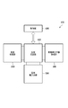
- FIG. 1 is a block diagram showing an organic monomolecular film forming apparatus for forming a SAM that is an organic monomolecular film on such a substrate
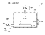
- FIG. 2 is a sectional view showing an example of a surface treatment unit 200
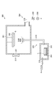
- FIG. 3 is an organic monomolecular film.
- 5 is a cross-sectional view showing an example of a film forming unit 300.
- an organic monomolecular film forming apparatus 100 includes a surface treatment unit 200 that performs surface treatment of a substrate, and an organic monomolecular film formation for forming an organic monomolecular film on the substrate after the surface treatment.
- This organic monomolecular film forming apparatus 100 is configured as a multi-chamber type apparatus.
- the substrate transfer unit 400 includes a transfer chamber held in a vacuum and a substrate transfer mechanism provided in the transfer chamber.
- the substrate carry-in / out unit 500 includes a substrate holding unit and a load lock chamber, conveys the substrate in the substrate holding unit to the load lock chamber, and carries in / out the substrate through the load lock chamber.
- the surface treatment unit 200 performs surface treatment of the substrate so that the surface state of the substrate on which the SAM is formed becomes a state in which a high-density SAM is formed by the SAM material (organic monomolecular film material) to be used.
- the plasma processing apparatus is configured to control the amounts of O and H on the surface portion of the substrate S.
- the surface treatment unit 200 includes a chamber 201, a substrate holder 202 that holds the substrate S in the chamber 201, and a plasma generation unit 203 that generates plasma and supplies the plasma into the chamber 201. And an exhaust mechanism 204 for evacuating the chamber 201.
- the side wall of the chamber 201 is provided with a loading / unloading port 211 that communicates with the transfer chamber for loading and unloading the substrate S.
- the loading / unloading port 211 can be opened and closed by a gate valve 212.
- the plasma generation unit 203 is supplied with a processing gas containing hydrogen gas, generates plasma containing hydrogen by an appropriate technique such as microwave plasma, inductively coupled plasma, capacitively coupled plasma, and supplies the plasma into the chamber 201.
- the exhaust mechanism 204 includes an exhaust pipe 213 connected to the lower portion of the chamber 201, a pressure adjustment valve 214 provided in the exhaust pipe 213, and a vacuum pump 215 that exhausts the inside of the chamber 201 through the exhaust pipe 213. ing.
- the substrate S is held on the substrate holder 202, the inside of the chamber 201 is held at a predetermined vacuum pressure, and in this state, plasma containing hydrogen is supplied from the plasma generation unit 203 into the chamber 201, whereby The surface is treated with plasma.
- plasma may be generated in the chamber 201, such as by generating a capacitively coupled plasma by providing parallel plate electrodes in the chamber 201.
- the organic monomolecular film forming unit 300 includes a chamber 301 for forming an organic monomolecular film on the substrate S therein, a substrate holder 302 for holding the substrate in the chamber 301, A SAM material supply system 303 for supplying the SAM material, and an exhaust system 304 for exhausting the interior of the chamber 301.
- a loading / unloading port 311 for loading / unloading the substrate S, which communicates with the transfer chamber, is provided on the side wall of the chamber 301, and the loading / unloading port 311 can be opened and closed by a gate valve 312.
- the substrate holder 302 is provided in the upper part of the chamber 301 and holds the substrate S so that the film formation surface faces downward.
- the substrate holder 302 may have a mechanism for heating the substrate S. When not heated, the substrate S is kept at room temperature.
- the SAM material supply system 303 includes a gas generation container 313, a SAM material storage container 314 provided in the gas generation container 313, a carrier gas introduction pipe 315 for introducing a carrier gas into the gas generation container 313, and a gas generation container And a SAM material gas supply pipe 316 that supplies the SAM material gas (organic monomolecular film material gas) generated in 313 into the chamber 301.
- the SAM material gas supply pipe 316 is provided so that the SAM material gas is discharged toward the substrate S from the tip thereof.
- the SAM material gas vaporized from the liquid SAM material L in the SAM material container 314 is conveyed by a carrier gas, and the gas containing the SAM material passes through the SAM material gas supply pipe 316 and in the vicinity of the substrate S in the chamber 301.
- a heater may be provided in the SAM material container 314.
- the exhaust system 304 includes an exhaust pipe 318 connected to the lower portion of the chamber 301, a pressure adjustment valve 319 provided in the exhaust pipe 318, and a vacuum pump 320 that exhausts the interior of the chamber 301 through the exhaust pipe 318. ing.
- the substrate S surface-treated by the surface treatment unit 200 is held on the substrate holder 302, the inside of the chamber 301 is held at a predetermined vacuum pressure, and in this state, the SAM material gas is supplied from the SAM material supply system 303 to the substrate S.
- the SAM material gas is supplied from the SAM material supply system 303 to the substrate S.
- the control unit 600 has a controller including a microprocessor (computer) that controls each component of the device 100.
- the controller controls the output of the surface treatment unit 200, the gas flow rate, the degree of vacuum, the flow rate of the carrier gas of the organic monomolecular film forming unit 300, the degree of vacuum, and the like.
- the controller is connected to a user interface having a keyboard for an operator to input commands for managing the device 100, a display for visualizing and displaying the operating status of the device 100, and the like.
- the controller causes each component of the apparatus 100 to execute a predetermined process in accordance with a control program and processing conditions for realizing a predetermined operation in the film forming process executed by the apparatus 100 under the control of the controller.
- a storage unit that stores a processing recipe, which is a control program, and various databases is connected.
- the processing recipe is stored in an appropriate storage medium in the storage unit. Then, if necessary, an arbitrary processing recipe is called from the storage unit and is executed by the controller, whereby a desired process in the apparatus 100 is performed under the control of the controller.
- FIG. 4 is a flowchart showing an organic monomolecular film forming method according to this embodiment.
- a self-assembled monomolecular film that is an organic monomolecular film is formed on the surface of an object to be processed having at least a surface structure having a network structure of Si and O.
- a substrate made of SiO 2 (glass) is prepared as such an object to be processed (step 1).
- step 2 surface treatment is performed on such a substrate S (step 2).
- the substrate S is transferred from the load lock chamber of the substrate carry-in / out unit 500 to the surface treatment unit 200 shown in FIG. 2 by the substrate transfer mechanism of the substrate transfer unit 400.
- the gate valve 212 is opened, the substrate S is loaded into the chamber 201 via the loading / unloading port 211, and placed on the substrate holder 202.
- plasma containing hydrogen generated in the plasma generation unit 203 is supplied into the chamber 201, and the surface of the substrate S is plasmad.
- Process plasma etching
- This surface treatment is for the surface state of the substrate S to be in a state where a high-density SAM can be obtained by the SAM material which is the organic monomolecular film material used in the organic monomolecular film forming unit 300.
- a SAM is formed on the substrate S that has been surface-treated (step 3).
- the substrate transport mechanism of the substrate transport unit 400 unloads the surface-treated substrate S from the chamber 201 and transports it to the organic single molecule forming unit 300.
- the gate valve 312 is opened and the substrate S is loaded into the chamber 301 via the loading / unloading port 311 and held on the substrate holder 302.
- the SAM material gas organic monomolecular film material gas
- the substrate transport mechanism of the substrate transport unit 400 unloads the substrate S on which the SAM is formed from the chamber 301 and transports it to the substrate holding unit through the load lock chamber of the substrate load / unload unit 500.
- a substance (silane coupling agent) composed of an organic molecule represented by the general formula R′—Si (O—R) 3 can be mentioned.
- R ′ is a functional group such as an alkyl group
- O—R is a hydrolyzable functional group such as a methoxy group or an ethoxy group.
- This OR functions as a binding site.
- An example of such a silane coupling agent is octamethyltrimethoxysilane (OTS).
- the substrate is exposed to the vapor of the SAM material, immersed in the SAM material solution, or the SAM material solution is applied to the substrate to adhere the SAM material onto the substrate. And proceed by leaving it in the atmosphere.
- SAM material is a compound having an organic molecule represented by the general formula R′—CH ⁇ CH 2 and having a C double bond at the terminal.
- R ′ is a functional group such as an alkyl group.
- the double bond is cleaved on the substrate surface by the following (3) and the end is bonded to Si.
- R′—CH ⁇ CH 2 + Si—H > R′—CH 2 —CH—Si (3)
- the surface state of the SAM material to be used with respect to a substrate having a surface structure with a network structure of Si and O is used. It was found that it is effective to perform surface treatment so that the bonding sites with the gas exist at a high density.
- the surface state where such binding sites exist at a high density is a surface state where a high-density SAM is obtained.
- the treatment with plasma containing hydrogen of the present embodiment (plasma etching) is performed, so that the stable network structure of Si and O on the substrate surface is destroyed, and the amount of H and the amount of O on the surface are reduced.
- the surface can be adjusted and the surface to which a given SAM material can easily react.
- the reaction of the above formula (3) proceeds at a portion where a Si—H bond is present, and a compound having a C double bond is bonded to the terminal. Since the Si—H bond exists not only on the outermost surface but also inside the first and second layers from the surface, the reaction of the formula (3) occurs inside, and a SAM material having a C double bond at the terminal is used. A high-density SAM can be formed.
- plasma containing hydrogen and oxygen is used as plasma containing hydrogen, such as plasma using H 2 gas + O 2 gas + rare gas (Ar gas), or plasma using H 2 gas + O 2 gas
- Ar gas rare gas
- FIG. 7 although Si on the surface is etched by hydrogen radicals and O is also detached, O is supplied to the surface by oxygen radicals in the plasma.
- FIG. 8 there are many O—H bonds in addition to Si—H bonds in the first and second layers from the outermost surface and from the surface, and bonding when a silane coupling agent is used as the SAM material. Sites can be formed with high density.
- the O—H bond (OH terminal) portion functions as a binding site where a conventional silane coupling reaction occurs, and the Si—H bond also functions as a binding site for the silane coupling agent.
- the binding sites of the ring agent can be present at a high density, and a SAM having a significantly higher density than before can be formed.
- a compound having a C double bond at the terminal is used as the SAM material. Therefore, it is difficult to obtain a high-density SAM.
- the surface state is bonded to the SAM material according to the SAM material.
- the site can be formed in a high density state, and the SAM can be formed at a high density on the surface having a network structure of Si and O.
- the SAM material when plasma treatment is used for the surface treatment of the substrate, a surface cleaning effect by plasma is obtained, so that the SAM material can be easily reacted also by the effect.
- a silane coupling agent when used as the SAM material, particles on the surface can be removed even if Ar gas plasma or H 2 gas plasma is used. Can do.
- the plasma in order to form a high-density SAM using a silane coupling agent as the SAM material, as described above, the plasma needs to be H 2 gas and O 2 gas.
- plasma treatment plasma etching
- wet treatment wet etching
- the amount of H and O on the surface can be controlled by appropriately selecting the treatment liquid.
- a Si—H bond can be formed on the surface having a network structure of Si and O.
- hydrogen atom treatment described below or heat treatment in a hydrogen atmosphere can also be used.
- Hydrogen gas is supplied to an ultra-high vacuum (1 ⁇ 10 ⁇ 6 Pa or less) vacuum chamber at about 1 ⁇ 10 ⁇ 4 Pa, and hydrogen molecules are dissociated into hydrogen atoms by thermal electrons or plasma. Adsorb to the substrate surface.
- the surface treatment process in step 2 and the SAM formation process in step 3 may be repeated a plurality of times.
- the SAM is formed in the second and subsequent SAM formation processes, and a higher density SAM can be formed.
- the wet treatment is preferable for the second and subsequent surface treatments.
- the surface treatment forms a region where the binding sites of the first SAM material exist at high density and a region where the binding sites of the second SAM material exist at high density
- the surface treatment is performed after the surface treatment.
- the first SAM material may be supplied to perform the first SAM formation step
- the second SAM material may be supplied to perform the second SAM formation step.
- the SAM is formed using a compound having a C double bond at the terminal in the second SAM formation step. It may be.
- the SAM by the silane coupling agent in a predetermined region in the first SAM formation step, the SAM by the compound having a C double bond is formed in another region in the second SAM formation step.
- a high-density SAM can be obtained.
- the first SAM material and the second SAM material may be supplied at a time, and the SAM may be formed in a surface state region corresponding to each.
- both a silane coupling agent as a SAM material and a compound having a C double bond at the terminal may be supplied at a time to form SAMs in different regions. This also makes it possible to form a higher density SAM.
- the SAM can be formed at a high density on the surface having the network structure of Si and O, so that the wear resistance such as an antifouling film is required. Can also be applied.
- an SiO 2 substrate (glass substrate) is prepared as a substrate having at least a surface portion having a network structure of Si and O, and Ar / H 2 gas plasma is irradiated on the SiO 2 substrate to treat the surface of the substrate. Went.
- the surface state with and without the plasma treatment was confirmed by TOF-SIMS mass spectrum.
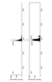
- FIGS. 9A and 9B are diagrams showing the vicinity of the mass number 30 of the TOF-SIMS mass spectrum at that time.
- FIG. 9A shows an unprocessed sample and
- FIG. 9B shows a plasma-processed sample.
- Example 2 a SAM was formed on the surface-treated substrate of Experimental Example 1 using CH 2 ⁇ CH— (OCF 2 CF 2 ) n which is a compound having a C double bond at the terminal as the SAM material.
- Sample A -(OCF 2 CF 2 ) n is perfluoroether (PFE) and is used as an antifouling film.
- a silane coupling agent (OCH 3 ) 3 —Si— (OCF 2 CF) is used as a SAM material on a SiO 2 substrate that has been subjected to dilute hydrofluoric acid (DHF) cleaning without plasma treatment.
- DHF dilute hydrofluoric acid
- SAM was formed using n (Sample B).
- (OCH 3 ) 3 —Si— (OCF 2 CF 2 ) n contains PFE in the molecule and is conventionally used for forming an antifouling film.
- Sample A could be formed because Si—H bonds were formed on the surface of the SiO 2 substrate. Moreover, about the sample B, SAM was formed by the long-time reaction which interposed water.
- a wear durability test was performed on samples A and B.
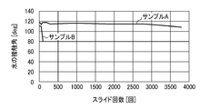
- the wear durability test was performed by an SW test in which a steel wool loaded with a weight was slid in a state of contact with the sample. Since the contact angle of water (hereinafter simply referred to as the contact angle) decreases as the film wears, the wear durability was evaluated based on the relationship between the number of slides and the contact angle. The result is shown in FIG. As shown in this figure, in Sample B, the number of slides was less than 100, the contact angle was 100 deg or less, and the wear resistance of the film was low. This is presumably because the reaction between the silane coupling agent and SiO 2 has low controllability with water interposed, and the density of the film was low.
- sample A the contact angle was maintained at 100 deg or more even when the number of slides exceeded 3500, and it was confirmed that the abrasion resistance of the film was significantly higher than that of sample B.
- the surface of the SiO 2 substrate is subjected to plasma treatment to form a Si—H bond, whereby CH 2 ⁇ CH— (OCF 2 CF, which is a compound having a Si double bond and a C double bond at the terminal. 2 )
- CH 2 ⁇ CH— OCF, which is a compound having a Si double bond and a C double bond at the terminal. 2
- a SAM is formed on an SiO 2 substrate subjected to various surface treatments using an OPTOOL (registered trademark) manufactured by Daikin Industries, Ltd., which is a silane coupling agent, as a SAM material, and samples C to H are formed. Produced.
- the substrates used for preparing Samples C to H are as follows.
- Sample C SiO 2 substrate sample D surface was DHF cleaning: Ar gas only in the generated plasma by surface-treated SiO 2 substrate
- Sample E SiO surface treated with plasma generated by using an Ar gas and H 2 gas 2 substrates
- Sample F SiO 2 substrate surface-treated with plasma generated using Ar gas and O 2 gas
- Sample G SiO surface-treated with plasma generated using Ar gas, H 2 gas, and O 2 gas 2 substrates
- Sample H SiO 2 substrate surface-treated with plasma generated using Ar gas, H 2 gas, and O 2 gas (O 2 gas flow rate increased from sample G)
- Table 1 summarizes the results of the SW test, which is the substrate surface treatment, initial contact angle, and wear durability test, in Samples C to H.
- Sample C in which the substrate surface was only subjected to DHF cleaning and was not subjected to plasma treatment, had an initial contact angle of 20 deg and a small amount of SAM.
- the initial contact angle was 115 deg and a film was formed.
- wear resistance the number of slides that can maintain a contact angle of 100 deg or more in the SW test. The number of slides is 100) and the wear durability is low, suggesting that the film density of the formed SAM is low.
- sample E In sample E in which the surface treatment was performed with plasma using Ar gas and H 2 gas, the initial contact angle was 115 deg, and the number of wear-resistant slides in the SW test was 1000 times less than that of sample D, but formed. The SAM film density is still not sufficient. Further, in sample F in which the surface treatment was performed with plasma using Ar gas and O 2 gas, the number of wear-resistant slides in the SW test was 100 times, which was similar to that of sample D. On the other hand, samples G and H in which the surface treatment was performed with plasma using Ar gas, H 2 gas, and O 2 gas had a contact angle of 100 deg or less as the number of wear-resistant slides in the SW test, which was 10,000 times or more. It is suggested that a SAM having high wear durability and high film density is formed. Among these, in Sample H in which the O 2 gas flow rate is increased from that in Sample G, the number of wear-resistant slides in the SW test is 20000, suggesting that the film density is particularly high.
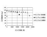
- a wear durability test was performed on the formed sample (sample K) by the SW test. The result is shown in FIG. As shown in this figure, the untreated sample I had an initial contact angle of 70 deg., Whereas the samples J and K were subjected to plasma treatment with Ar gas, H 2 gas, and O 2 gas. Indicates that the wear durability is extremely high, suggesting that a high-density SAM is obtained.
- the present invention can be variously modified without being limited to the above embodiment.
- a plasma treatment mainly containing hydrogen is used as a surface treatment of a substrate, and a silane coupling agent and a compound having a carbon double bond at a terminal is used as a film forming material
- the surface treatment of the substrate and the film forming material are not particularly limited as long as the surface state of the substrate is in a state in which binding sites with the film forming material to be used are present at a high density.
- an example of forming a SAM is an organic monomolecular film on a SiO 2 substrate, as long as the surface having the network structure of Si and O exists, the object to be processed is SiO It is not limited to two substrates. Further, the form of the object to be processed is not limited to the substrate. For example, by applying the present invention to a container-like object to be processed, a container having a modified surface can be manufactured.
Landscapes
- Chemical & Material Sciences (AREA)
- Engineering & Computer Science (AREA)
- Manufacturing & Machinery (AREA)
- Health & Medical Sciences (AREA)
- General Health & Medical Sciences (AREA)
- Toxicology (AREA)
- Organic Chemistry (AREA)
- Chemical Kinetics & Catalysis (AREA)
- Materials Engineering (AREA)
- Application Of Or Painting With Fluid Materials (AREA)
- Chemical Vapour Deposition (AREA)
- Electroluminescent Light Sources (AREA)
- Physical Or Chemical Processes And Apparatus (AREA)
- Drying Of Semiconductors (AREA)
- Physics & Mathematics (AREA)
- Plasma & Fusion (AREA)
Abstract
少なくとも表面部分がSiとOとのネットワーク構造である被処理体の表面に有機単分子膜を形成するにあたり、被処理体に対し、その表面状態が、用いようとする有機単分子膜材料の結合サイトが高密度で存在する状態となるような表面処理を行い、次いで表面処理後の被処理体に有機単分子膜材料を供給して被処理体の表面に有機単分子膜を形成する。
Description
本発明は、自己組織化単分子膜に代表される有機単分子膜を形成する有機単分子膜形成方法、および有機単分子膜を形成するための表面処理方法に関する。
近年、種々の分野で有機化合物からなる有機薄膜が用いられている。例えば、有機トランジスタのような有機半導体に用いられる有機半導体膜等が例示される。
このような有機化合物からなる有機薄膜としては、自己組織的に形成される高い秩序性を有する有機単分子膜である自己組織化単分子膜(Self-Assembled Monolayer:SAM)が知られている。
自己組織化単分子膜とは、所定の基板に対し、所定の化学結合を形成する官能基を末端基として有する有機分子を用いることにより、その基板の表面に対して、化学結合を形成させ、アンカリングされた有機分子が基板表面からの規制および有機分子間の相互作用によって、秩序的に配列した状態となり、単分子膜となったものをいう。
このような自己組織化単分子膜は、有機半導体膜自体としてばかりでなく、物質表面の改質に有効であり、例えば有機トランジスタの基板表面を改質(濡れ性・親油性を制御)して有機トランジスタの電気特性を向上させる用途等への利用が考えられている。
特許文献1には、シランカップリング剤を用いた自己組織化単分子膜をSiO2系の基板上に形成して表面を改質することが記載されている。シランカップリング剤を用いた自己組織化単分子膜は、アルキル基や、フッ化アルキル基を有機官能基として有し、基板表面を撥水性に改質する用途に用いることができる。
また、特許文献1には、シランカップリング剤を用いた自己組織化単分子膜が、基板をシランカップリング剤の蒸気に暴露する方法、基板をシランカップリング剤溶液に浸漬する方法、基板にシランカップリング剤を塗布する方法等の極めて簡便な方法で形成できることが記載されている。
一方、特許文献2には、ポリシリコン層の表面を水素終端化させ、水素終端化された表面に、末端に炭素の二重結合を持つ有機分子を供給し、Siと反応させて、自己組織化単分子膜を形成する方法が開示されている。
ところで、このような有機単分子膜は、種々の用途への適用が検討されており、例えば、防汚膜のように、有機単分子膜を高密度で形成することが要求される用途もある。
しかし、特許文献1の手法で、SiO2上にSAMを形成するためには、気体や液体のシランカップリング剤を基板表面に吸着させた後に基板のSiとシランカップリング反応を生じさせるが、この際の反応は空気中の水分の存在下で極めて緩慢に進行するものであり、膜形成の制御性が悪く、SAMを高密度で形成することが困難である。
また、特許文献2の手法では、水素終端化されたSiの表面に比較的高密度で膜形成することができるものの、SiO2のようにSiとOのネットワーク構造を有する被処理体の表面では反応が生じ難く、SAMを形成することは極めて困難である。
したがって、本発明の目的は、少なくとも表面部分がSiとOのネットワーク構造を有する被処理体の表面に有機単分子膜を高密度で形成することができる有機単分子膜形成方法、およびこのような有機単分子膜を形成するための表面処理方法を提供することにある。
すなわち、本発明の第1の観点によれば、少なくとも表面部分がSiとOとのネットワーク構造である被処理体の表面に有機単分子膜を形成する有機単分子膜形成方法であって、被処理体に対し、その表面状態が、用いようとする有機単分子膜材料の結合サイトが高密度で存在する状態となるような表面処理を行うことと、前記表面処理後の被処理体に前記有機単分子膜材料を供給して被処理体の表面に有機単分子膜を形成することとを有する有機単分子膜形成方法が提供される。
本発明の第2の観点によれば、少なくとも表面部分がSiとOとのネットワーク構造である被処理体の表面に有機単分子膜を形成する有機単分子膜形成方法であって、被処理体の表面にSi-H結合を形成する表面処理を行うことと、前記表面処理後の被処理体に、末端にCの二重結合を有する化合物を供給して被処理体の表面に有機単分子膜を形成することとを有する有機単分子膜形成方法が提供される。
本発明の第3の観点によれば、少なくとも表面部分がSiとOとのネットワーク構造である被処理体の表面に有機単分子膜を形成する有機単分子膜形成方法であって、被処理体の表面にO-H結合およびSi-H結合を形成する表面処理を行うことと、前記表面処理後の被処理体に、シランカップリング剤を供給して被処理体の表面に有機単分子膜を形成することとを有する有機単分子膜形成方法が提供される。
本発明の第4の観点によれば、少なくとも表面部分がSiとOとのネットワーク構造である被処理体の表面に有機単分子膜材料を供給して有機単分子膜を形成するに先立って、被処理体に対し、その表面状態が、用いようとする有機単分子膜材料の結合サイトが高密度で存在する状態となるような表面処理を行う表面処理方法が提供される。
本発明の第5の観点によれば、少なくとも表面部分がSiとOとのネットワーク構造である被処理体の表面に有機単分子膜材料として末端にCの二重結合を有する化合物を供給して有機単分子膜を形成するに先立って、被処理体の表面にSi-H結合を形成する表面処理を行う表面処理方法が提供される。
本発明の第6の観点によれば、少なくとも表面部分がSiとOとのネットワーク構造である被処理体の表面に有機単分子膜材料としてシランカップリング剤を供給して有機単分子膜を形成するに先立って、被処理体を表面処理する表面処理方法であって、被処理体の表面にO-H結合およびSi-H結合を形成する表面処理を行う表面処理方法を提供する。
本発明によれば、少なくとも表面部分がSiとOとのネットワーク構造である被処理体の表面に有機単分子膜を形成するにあたり、被処理体に対し、その表面状態が、用いようとする有機単分子膜材料の結合サイトが高密度で存在する状態となるような表面処理を行うので、被処理体に対して高密度で有機単分子膜を形成することができる。
以下、添付図面を参照して本発明の実施形態について説明する。
<有機単分子膜形成装置>
最初に、本発明の一実施形態に係る有機単分子膜の形成方法を実施するための有機単分子膜形成装置の一例について説明する。
<有機単分子膜形成装置>
最初に、本発明の一実施形態に係る有機単分子膜の形成方法を実施するための有機単分子膜形成装置の一例について説明する。
本実施形態に係る有機単分子膜形成装置は、少なくとも表面部分がSiとOのネットワーク構造を有する被処理体の表面に有機単分子膜である自己組織化単分子膜(SAM)を形成するものである。このような被処理体としてSiO2(ガラス)製の基板を用いる。図1は、そのような基板に有機単分子膜であるSAMを形成する有機単分子膜形成装置を示すブロック図、図2は表面処理部200の一例を示す断面図、図3は有機単分子膜形成部300の一例を示す断面図である。
図1に示すように、有機単分子膜形成装置100は、基板の表面処理を行う表面処理部200と、表面処理した後の基板上に有機単分子膜を形成するための有機単分子膜形成部300と、表面処理部200および有機単分子膜形成部300に対する基板の搬送を行う基板搬送部400と、基板の搬入出を行う基板搬入出部500と、有機単分子膜形成装置100の各構成部を制御する制御部600とを有する。この有機単分子膜形成装置100は、マルチチャンバ型の装置として構成される。基板搬送部400は、真空に保持される搬送室と、搬送室内に設けられた基板搬送機構とを有している。基板搬入出部500は、基板保持部とロードロック室とを有し、基板保持部の基板をロードロック室へ搬送し、ロードロック室を介して基板の搬入出を行う。
表面処理部200は、SAMを形成する基板の表面状態が、用いるSAM材料(有機単分子膜材料)により高密度のSAMが形成される状態となるように、基板の表面処理を行うものであり、本例では基板Sの表面部分のOとHの量を制御するプラズマ処理装置として構成される。
この表面処理部200は、図2に示すように、チャンバ201と、チャンバ201内で基板Sを保持する基板ホルダ202と、プラズマを生成してチャンバ201内にプラズマを供給するプラズマ生成部203と、チャンバ201内を真空排気するための排気機構204とを有する。
チャンバ201の側壁には、搬送室に連通する、基板Sを搬入出するための搬入出口211が設けられており、搬入出口211はゲートバルブ212により開閉可能となっている。
プラズマ生成部203は、水素ガスを含む処理ガスが供給され、マイクロ波プラズマ、誘導結合プラズマ、容量結合プラズマ等の適宜の手法で水素を含むプラズマを生成してチャンバ201内に供給する。
排気機構204は、チャンバ201の下部に接続された排気管213と、排気管213に設けられた圧力調整バルブ214と、排気管213を介してチャンバ201内を排気する真空ポンプ215とを有している。
そして、基板Sを基板ホルダ202上に保持させ、チャンバ201内を所定の真空圧力に保持し、その状態でプラズマ生成部203から水素を含むプラズマをチャンバ201内に供給することにより、基板Sの表面がプラズマにより処理される。
なお、プラズマ生成部203を設ける代わりに、チャンバ201内に平行平板電極を設けて容量結合プラズマを生成する等、チャンバ201内でプラズマを生成してもよい。
有機単分子膜形成部300は、図3に示すように、その中で基板S上に有機単分子膜を形成するチャンバ301と、チャンバ301内で基板を保持する基板ホルダ302と、チャンバ301内にSAM材料を供給するためのSAM材料供給系303と、チャンバ301内を排気する排気系304とを有する。
チャンバ301の側壁には、搬送室に連通する、基板Sを搬入出するための搬入出口311が設けられており、搬入出口311はゲートバルブ312により開閉可能となっている。
基板ホルダ302は、チャンバ301内の上部に設けられ、基板Sを、その膜形成面が下方に向くように保持するようになっている。基板ホルダ302は基板Sを加熱する機構を有していてもよい。加熱されない場合には、基板Sは室温に保持される。
SAM材料供給系303は、ガス生成容器313と、ガス生成容器313内に設けられたSAM材料収容容器314と、ガス生成容器313内にキャリアガスを導入するキャリアガス導入管315と、ガス生成容器313内で生成されたSAM材料ガス(有機単分子膜材料ガス)をチャンバ301内に供給するSAM材料ガス供給管316とを有する。SAM材料ガス供給管316は、その先端からSAM材料ガスが基板Sに向けて吐出されるように設けられている。そして、SAM材料収容容器314内の液体状のSAM材料Lから気化したSAM材料ガスをキャリアガスにより搬送し、SAM材料を含むガスを、SAM材料ガス供給管316を経てチャンバ301内の基板S近傍に供給する。気化が不十分な場合や、SAM材料が常温で固体の場合には、SAM材料収容容器314にヒーターを設けてもよい。
排気系304は、チャンバ301の下部に接続された排気管318と、排気管318に設けられた圧力調整バルブ319と、排気管318を介してチャンバ301内を排気する真空ポンプ320とを有している。
そして、表面処理部200により表面処理された基板Sを基板ホルダ302上に保持させ、チャンバ301内を所定の真空圧力に保持し、その状態でSAM材料供給系303からSAM材料ガスを基板Sの近傍に供給することにより、基板Sの表面に有機単分子膜としてSAMが形成される。
制御部600は、装置100の各構成部を制御するマイクロプロセッサ(コンピュータ)を備えたコントローラを有している。コントローラは、例えば表面処理部200の出力、ガス流量、真空度、有機単分子膜形成部300のキャリアガスの流量、真空度等を制御するようになっている。コントローラには、オペレータが装置100を管理するためにコマンドの入力操作等を行うキーボードや、装置100の稼働状況を可視化して表示するディスプレイ等を有するユーザーインターフェースが接続されている。また、コントローラには、装置100で実行される膜形成処理における所定の操作をコントローラの制御にて実現するための制御プログラムや処理条件に応じて装置100の各構成部に所定の処理を実行させるための制御プログラムである処理レシピや、各種データベース等が格納された記憶部が接続されている。処理レシピは記憶部の中の適宜の記憶媒体に記憶されている。そして、必要に応じて、任意の処理レシピを記憶部から呼び出してコントローラに実行させることで、コントローラの制御下で、装置100での所望の処理が行われる。
<有機単分子膜形成方法>
次に、上記有機単分子膜形成装置を用いた有機単分子膜形成方法について説明する。図4は、本実施形態に係る有機単分子膜形成方法を示すフローチャートである。
次に、上記有機単分子膜形成装置を用いた有機単分子膜形成方法について説明する。図4は、本実施形態に係る有機単分子膜形成方法を示すフローチャートである。
本実施形態は、上述したように、少なくとも表面部分がSiとOのネットワーク構造を有する被処理体の表面に有機単分子膜である自己組織化単分子膜(SAM)を形成するものであり、このような被処理体としてSiO2(ガラス)製の基板を準備する(ステップ1)。
そして、このような基板Sに対し表面処理を行う(ステップ2)。表面処理に際しては、まず、基板Sを基板搬入出部500のロードロック室から基板搬送部400の基板搬送機構により、図2に示す表面処理部200へ搬送する。この際に、ゲートバルブ212を開けて搬入出口211を介して基板Sをチャンバ201内に搬入し、基板ホルダ202上に載置する。この状態で、排気機構204による排気量を調整してチャンバ201内の圧力を制御しつつ、プラズマ生成部203において生成された水素を含むプラズマをチャンバ201内に供給し、基板Sの表面をプラズマ処理(プラズマエッチング)する。
この表面処理は、基板Sの表面状態が、有機単分子膜形成部300において用いる有機単分子膜材料であるSAM材料により高密度のSAMが得られる状態となるようにするためのものである。
この処理の後、表面処理が施された基板Sに対し、SAMを形成する(ステップ3)。SAMの形成に際しては、基板搬送部400の基板搬送機構により、表面処理された基板Sをチャンバ201から搬出し、有機単分子形成部300へ搬送する。この際に、ゲートバルブ312を開けて搬入出口311を介して基板Sをチャンバ301内に搬入し、基板ホルダ302上に保持させる。この状態で、排気機構304による排気量を調整してチャンバ301内の圧力を制御しつつ、SAM材料供給系303によりSAM材料Lから気化したSAM材料ガス(有機単分子膜材料ガス)をキャリアガスにより搬送し、チャンバ301内の基板S近傍に供給する。これにより、基板Sの表面に有機単分子膜であるSAMを高密度で形成することができる。
この後、基板搬送部400の基板搬送機構により、SAMが形成された基板Sをチャンバ301から搬出し、基板搬入出部500のロードロック室を経て基板保持部へ搬送する。
<基板の表面処理>
次に、上記有機単分子膜形成方法の中で特に重要な基板の表面処理について詳細に説明する。
SAMを形成するに当たっては、SAM材料として、基板の表面と化学結合を形成する結合サイトを有する有機分子からなるものを用いる。
次に、上記有機単分子膜形成方法の中で特に重要な基板の表面処理について詳細に説明する。
SAMを形成するに当たっては、SAM材料として、基板の表面と化学結合を形成する結合サイトを有する有機分子からなるものを用いる。
典型的な例として、一般式R′-Si(O-R)3で表される有機分子からなる物質(シランカップリング剤)を挙げることができる。ここで、R′はアルキル基等の官能基であり、O-Rは、加水分解可能な官能基、例えばメトキシ基、エトキシ基である。このO-Rが、結合サイトとして機能する。このようなシランカップリング剤としては、例えばオクタメチルトリメトキシシラン(OTS)を挙げることができる。
シランカップリング剤を用いたSAMの形成においては、SiとOとのネットワーク構造を有する表面、典型的にはSiO2(ガラス)基板の表面で、シランカップリングと呼ばれる次の(1)、(2)の反応を生じさせる。
R′-Si(O-R)3+H2O⇒R′-Si(OH)3+ROH (1)
R′-Si(OH)3+SiO(表面)⇒R′-SiO+Si(表面)+H2O (2)
R′-Si(O-R)3+H2O⇒R′-Si(OH)3+ROH (1)
R′-Si(OH)3+SiO(表面)⇒R′-SiO+Si(表面)+H2O (2)
この反応により、SiO2表面に単分子のアルキル基等の官能基(R′)が付着し、表面物性が変化する。上記一連の反応は、一段階目の(1)の反応でSAM材料を加水分解し、二段階目の(2)の反応で基板と縮重合するという2段階の反応である。
上記(1)、(2)の反応は、基板をSAM材料の蒸気に暴露したり、SAM材料溶液に浸漬したり、基板にSAM材料溶液を塗布したりして、SAM材料を基板上に付着させ、大気中に放置することにより進行させることができる。
これらの方法は、材料を基板に付着させておけば反応が進行するため、コスト的には有利であるが、反応が極めて遅く、また、大気中の水分を使うため、膜形成の際の制御性が悪い。このため、基板上に高密度でSAMを形成することが困難である。
また、SAM材料の他の例として、一般式R′-CH=CH2で表される有機分子からなる、末端がCの二重結合を有する化合物を挙げることもできる。R′は、アルキル基等の官能基である。このような末端にCの二重結合を有するSAM材料は、以下の(3)により基板表面で二重結合が開裂してその末端がSiと結合する。
R′-CH=CH2+Si-H⇒R′-CH2-CH-Si (3)
R′-CH=CH2+Si-H⇒R′-CH2-CH-Si (3)
この反応は水を介在させないため制御性が良く、高密度化も可能である。しかし、この反応を生じさせるためには、基板表面にSi-H結合が形成されていることが必要であるため、SiO2基板の表面のようなSiとOとのネットワーク構造を有する表面に直接膜形成することは困難である。
このように、従来は、一般的なSAM材料を用いて、SiとOとのネットワーク構造を有する表面に高密度でSAMを形成することは困難であった。
そこで、一般的なSAM材料を用いて制御性良く高密度のSAMを形成する方法を検討した結果、表面部分がSiとOとのネットワーク構造を有する基板に対し、その表面状態が、用いるSAM材料ガスとの結合サイトが高密度で存在する状態となるような表面処理を行うことが有効であるという知見が得られた。このような結合サイトが高密度で存在する表面状態は、すなわち高密度のSAMが得られる表面状態である。
基板表面処理として、本実施形態の水素を含むプラズマによる処理(プラズマエッチング)を行うことにより、基板表面の安定なSiとOとのネットワーク構造を崩して、表面のHの量およびOの量を調整することができ、所定のSAM材料が反応しやすい表面とすることができる。
例えば、水素を含むプラズマとして、H2ガス+希ガス(Arガス)によるプラズマ、またはH2ガス単独のプラズマのように、水素を含み酸素を含まないプラズマを用いる場合には、図5に示すように、SiとOとのネットワーク構造を有する表面のSiがプラズマ中の水素ラジカルによりエッチングされ、それにともなってOの離脱も生じ、水素ラジカルは最表面のみならず内部にも侵入する。このため、結果的に、図6に示すように表面部分がSi-H結合の多い状態となる。Si-H結合は、末端にCの二重結合を有する化合物の結合サイトとして機能する。すなわち、Si-H結合が存在する部分で上述の(3)式の反応が進行して末端にCの二重結合を有する化合物が結合する。そして、Si-H結合は最表面のみならず表面から1、2層内部にも存在するので、内部でも(3)式の反応が生じ、末端にCの二重結合を有するSAM材料を用いて高密度のSAMを形成することができる。
一方、H2ガス+希ガス(Arガス)のプラズマ、またはH2ガス単独のプラズマを用いてプラズマ処理(プラズマエッチング)を行った場合の図6に示す表面状態は、プラズマにより表面がSiとOとのネットワーク構造から多くのOが脱落した状態であり、SAM材料としてシランカップリング剤を用いた場合には、結合サイトの密度が十分ではない。
これに対して、水素を含むプラズマとして、H2ガス+O2ガス+希ガス(Arガス)によるプラズマ、またはH2ガス+O2ガスによるプラズマのように、水素および酸素を含むプラズマを用いると、図7に示すように、水素ラジカルにより表面のSiがエッチングされ、Oの離脱も生じるものの、プラズマ中の酸素ラジカルにより表面にOが供給される。このため、図8に示すように、最表面および表面から1、2層内部にはSi-H結合の他にO-H結合が多く存在し、SAM材料としてシランカップリング剤を用いる場合の結合サイトを高密度で形成することができる。すなわち、O-H結合(O-H終端)の部分は、従来のシランカップリング反応が生じる結合サイトとして機能し、さらにSi-H結合もシランカップリング剤の結合サイトとして機能するから、シランカップリング剤の結合サイトを高密度で存在させることができ、従来よりも著しく高密度のSAMを形成することができる。ただし、図8の状態では、表面に存在するOの量が多くなり、上記(3)の反応が生じるサイトが少なくなるため、SAM材料として末端がCの二重結合を有する化合物を用いた場合には、高密度のSAMは得難い。
このように、基板Sに表面処理を施して、SiとOとのネットワーク構造を有する表面部分のH量およびO量を適切に制御することにより、表面状態をSAM材料に応じてSAM材料の結合サイトが高密度で形成された状態とすることができ、SiとOとのネットワーク構造を有する表面に高密度でSAMを形成することが可能となる。
なお、基板の表面処理にプラズマ処理を用いる場合には、プラズマによる表面洗浄効果が得られるため、その効果によってもSAM材料を反応しやすくすることができる。例えば、SAM材料としてシランカップリング剤を用いた場合に、ArガスのプラズマやH2ガスのプラズマを用いても表面のパーティクルを除去できるので、無処理の場合よりもSAMの密度を多少上げることができる。ただし、SAM材料としてシランカップリング剤を用いて高密度のSAMを形成するためには、上述のように、H2ガスとO2ガスによるプラズマであることが必要である。
以上の例では、表面処理としてプラズマ処理(プラズマエッチング)を用いたが、ウエット処理(ウエットエッチング)を用いてもよい。ウエット処理の場合には、処理液を適切に選択することにより、表面のHの量とOの量とを制御することができる。
SAM材として末端がCの二重結合を有する化合物を用いた場合には、SiとOとのネットワーク構造を有する表面にSi-H結合が形成することができればよいので、表面処理として、以上のようなプラズマ処理やウエット処理の他に、以下に説明する水素原子処理、または水素雰囲気中の加熱処理を用いることもできる。
・水素原子処理
超高真空(1×10⁻⁶Pa以下)の真空チャンバに水素ガスを1×10⁻⁴Pa程度供給し、熱電子あるいはプラズマで水素分子を水素原子に解離させて水素原子を基板表面に吸着させる。
超高真空(1×10⁻⁶Pa以下)の真空チャンバに水素ガスを1×10⁻⁴Pa程度供給し、熱電子あるいはプラズマで水素分子を水素原子に解離させて水素原子を基板表面に吸着させる。
・水素雰囲気中の加熱処理
真空引きの際に、水素をキャリアガスとして流すことでチャンバの大気を水素ガスに置換して水素雰囲気の真空状態を作成し、この雰囲気中で基板を400℃程度に加熱し、水素を基板表面に吸着させる。
真空引きの際に、水素をキャリアガスとして流すことでチャンバの大気を水素ガスに置換して水素雰囲気の真空状態を作成し、この雰囲気中で基板を400℃程度に加熱し、水素を基板表面に吸着させる。
なお、より高密度のSAMを形成する観点から、ステップ2の表面処理工程とステップ3のSAM形成工程を複数回繰り返してもよい。これにより、1回目のSAM形成工程の際にSAMが形成されなかった領域においても、2回目以降のSAM形成工程によりSAMが形成され、より高密度のSAMを形成することができる。ただし、2回目以降の表面処理の際にプラズマを用いると1回目に形成されたSAMが損傷するおそれがあるので、2回目以降の表面処理にはウエット処理が好ましい。
また、表面処理により、第1のSAM材料の結合サイトが高密度で存在する領域と第2のSAM材料の結合サイトが高密度で存在する領域とが形成される場合には、表面処理の後、第1のSAM材料を供給して1回目のSAM形成工程を行い、引き続き第2のSAM材料を供給して2回目のSAM形成工程を行ってもよい。例えば、1回目のSAM形成工程でSAM材料としてシランカップリング剤を用いてSAMを形成した後、2回目のSAM形成工程で末端にCの二重結合を有する化合物を用いてSAMを形成するようにしてもよい。これにより、1回目のSAM形成工程でシランカップリング剤によるSAMを所定領域に形成した後、2回目のSAM形成工程でCの二重結合を有する化合物によるSAMを他の領域に形成することができ、高密度のSAMを得ることができる。また、第1のSAM材料と第2のSAM材料を一度に供給して、それぞれに対応する表面状態の領域にSAMを形成するようにしてもよい。例えば、SAM材料としてシランカップリング剤および末端にCの二重結合を有する化合物の両方を一度に供給して、それぞれ異なる領域にSAMを形成するようにしてもよい。これによっても、より高密度のSAMを形成することができる。
以上のように、本実施形態によれば、SiとOとのネットワーク構造を有する表面にSAMを高密度で形成することができるので、防汚膜のような耐摩耗性が要求される用途にも適用することができる。
<実験例>
次に、実験例について説明する。
次に、実験例について説明する。
[実験例1]
ここでは、少なくとも表面部分がSiとOとのネットワーク構造を有する基板としてSiO2基板(ガラス基板)を準備し、このSiO2基板に、Ar/H2ガスのプラズマを照射して基板の表面処理を行った。このプラズマ処理の有無による表面状態をTOF-SIMSマススペクトルにて確認した。図9は、その際のTOF-SIMSマススペクトルのマスナンバー30付近を示す図であり、(a)は未処理のもの、(b)はプラズマ処理を行ったものである。(a)のように未処理では、Siの同位体である30Siのピークだけが見られるが、(b)のようにプラズマ処理後では30Siの他にSiH2(29.99amu)の信号が見られる。これらのスペクトルから、水素を含むプラズマを照射することにより、基板表面部分にSi-H結合が形成されたことがわかる。
ここでは、少なくとも表面部分がSiとOとのネットワーク構造を有する基板としてSiO2基板(ガラス基板)を準備し、このSiO2基板に、Ar/H2ガスのプラズマを照射して基板の表面処理を行った。このプラズマ処理の有無による表面状態をTOF-SIMSマススペクトルにて確認した。図9は、その際のTOF-SIMSマススペクトルのマスナンバー30付近を示す図であり、(a)は未処理のもの、(b)はプラズマ処理を行ったものである。(a)のように未処理では、Siの同位体である30Siのピークだけが見られるが、(b)のようにプラズマ処理後では30Siの他にSiH2(29.99amu)の信号が見られる。これらのスペクトルから、水素を含むプラズマを照射することにより、基板表面部分にSi-H結合が形成されたことがわかる。
[実験例2]
次に、実験例1の表面処理を施した基板に、SAM材料として、末端にCの二重結合を有する化合物であるCH2=CH-(OCF2CF2)nを用いてSAMを形成した(サンプルA)。-(OCF2CF2)nはパーフルオロエーテル(PFE)であり、防汚膜として利用されるものである。比較のため、プラズマ処理を行わずに、希フッ酸(DHF)洗浄を行っただけのSiO2基板に、SAM材料として、シランカップリング剤である(OCH3)3-Si-(OCF2CF2)nを用いてSAMを形成した(サンプルB)。(OCH3)3-Si-(OCF2CF2)nは、分子中にPFEを含み、防汚膜形成用として従来から用いられているものである。
次に、実験例1の表面処理を施した基板に、SAM材料として、末端にCの二重結合を有する化合物であるCH2=CH-(OCF2CF2)nを用いてSAMを形成した(サンプルA)。-(OCF2CF2)nはパーフルオロエーテル(PFE)であり、防汚膜として利用されるものである。比較のため、プラズマ処理を行わずに、希フッ酸(DHF)洗浄を行っただけのSiO2基板に、SAM材料として、シランカップリング剤である(OCH3)3-Si-(OCF2CF2)nを用いてSAMを形成した(サンプルB)。(OCH3)3-Si-(OCF2CF2)nは、分子中にPFEを含み、防汚膜形成用として従来から用いられているものである。
サンプルAについては、SiO2基板の表面にSi-H結合が形成されているため、膜形成が可能であった。また、サンプルBについては、水を介在させた長時間の反応によりSAMが形成された。
次に、サンプルA、Bについて、摩耗耐久性試験を行った。摩耗耐久性試験は、サンプルに対し、重りを載せたスチールウールを接触させた状態でスライドさせるSWテストにより行った。膜が摩耗すると水の接触角(以下単に接触角と記す)が低下していくため、スライド回数と接触角との関係により摩耗耐久性を評価した。その結果を図10に示す。この図に示すように、サンプルBでは、スライド回数が100回未満で接触角が100deg以下となり膜の摩耗耐久性が低いものとなった。これは、シランカップリング剤とSiO2との反応が水を介在させた制御性の低いものであり、膜の密度が低かったためと考えられる。これに対し、サンプルAでは、スライド回数が3500回を超えても接触角100deg以上を維持しており、膜の摩耗耐久性がサンプルBよりも著しく高いことが確認された。これは、SiO2基板の表面をプラズマ処理してSi-H結合を形成させることにより、そのSi-Hと、末端にCの二重結合を有する化合物であるCH2=CH-(OCF2CF2)nとが反応し、サンプルBよりも膜密度の高いSAMが形成されたことを示唆するものである。
[実験例3]
ここでは、種々の表面処理を行ったSiO2基板に対し、SAM材料として、シランカップリング剤であるダイキン工業株式会社製のオプツール(登録商標)を用いてSAMを形成し、サンプルC~Hを作製した。サンプルC~Hの作製に用いた基板は以下のとおりである。
サンプルC:表面をDHF洗浄したSiO2基板
サンプルD:Arガスのみで生成されたプラズマにより表面処理したSiO2基板
サンプルE:ArガスとH2ガスを用いて生成されたプラズマにより表面処理したSiO2基板
サンプルF:ArガスとO2ガスを用いて生成されたプラズマにより表面処理したSiO2基板
サンプルG:ArガスとH2ガスとO2ガスを用いて生成されたプラズマにより表面処理したSiO2基板
サンプルH:ArガスとH2ガスとO2ガスを用いて生成されたプラズマにより表面処理したSiO2基板(サンプルGよりもO2ガス流量を増加)
ここでは、種々の表面処理を行ったSiO2基板に対し、SAM材料として、シランカップリング剤であるダイキン工業株式会社製のオプツール(登録商標)を用いてSAMを形成し、サンプルC~Hを作製した。サンプルC~Hの作製に用いた基板は以下のとおりである。
サンプルC:表面をDHF洗浄したSiO2基板
サンプルD:Arガスのみで生成されたプラズマにより表面処理したSiO2基板
サンプルE:ArガスとH2ガスを用いて生成されたプラズマにより表面処理したSiO2基板
サンプルF:ArガスとO2ガスを用いて生成されたプラズマにより表面処理したSiO2基板
サンプルG:ArガスとH2ガスとO2ガスを用いて生成されたプラズマにより表面処理したSiO2基板
サンプルH:ArガスとH2ガスとO2ガスを用いて生成されたプラズマにより表面処理したSiO2基板(サンプルGよりもO2ガス流量を増加)
表1に、サンプルC~Hにおける、基板の表面処理、イニシャルの接触角、および摩耗耐久性試験であるSWテストの結果をまとめて示す。
表1に示すように、基板表面をDHF洗浄したのみでプラズマ処理を行わなかったサンプルCでは、イニシャルの接触角が20degであり、SAMがわずかしか形成されていないことが確認された。また、表面処理をArガスのみのプラズマで行ったサンプルDでは、イニシャルの接触角が115degであり膜形成はされていたが、SWテストで接触角100deg以上を維持できるスライド回数(以下、耐摩耗スライド回数という)が100回と摩耗耐久性が低いものであり、形成されたSAMの膜密度が低いことを示唆している。表面処理をArガスとH2ガスによるプラズマで行ったサンプルEでは、イニシャルの接触角が115degであり、SWテストでの耐摩耗スライド回数はサンプルDよりは多いものの1000回と少なく、形成されたSAMの膜密度が未だ十分とはいえない。また、表面処理をArガスとO2ガスによるプラズマで行ったサンプルFでは、SWテストにおける耐摩耗スライド回数が100回とサンプルDと同程度であった。これらに対して、表面処理をArガスとH2ガスとO2ガスによるプラズマで行ったサンプルG、Hは、SWテストにおける耐摩耗スライド回数で接触角が100deg以下となる回数が10000回以上と摩耗耐久性が高く、膜密度の高いSAMが形成されていることが示唆されている。これらの中でも、O2ガス流量をサンプルGよりも増加させたサンプルHでは、SWテストにおける耐摩耗スライド回数が20000回となり、膜密度が特に高いことが示唆されている。

[実験例4]
次に、SiO2基板にDHF洗浄のみを行ってプラズマ処理を行わずに、SAM材料として、シランカップリング剤であるダイキン工業株式会社製のオプツール(登録商標)を用いてSAMを形成したサンプル(サンプルI)と、SiO2基板にArガスとH2ガスとO2ガスを用いてチャンバ内圧力を6.7Paとした条件でプラズマ処理(処理A)した後、同様にSAMを形成したサンプル(サンプルJ)と、SiO2基板にArガスとH2ガスとO2ガスを用いて処理Aとは異なり、チャンバ内圧力を100Paとした条件でプラズマ処理(処理B)した後、同様にSAMを形成したサンプル(サンプルK)とについて、上記SWテストにより摩耗耐久性試験を行った。その結果を図11に示す。この図に示すように、未処理のサンプルIでは、イニシャルの接触角が70degと不十分であったのに対し、ArガスとH2ガスとO2ガスによるプラズマ処理を施したサンプルJ、Kは、摩耗耐久性が極めて高いことが把握され、高密度のSAMが得られていることを示唆している。
次に、SiO2基板にDHF洗浄のみを行ってプラズマ処理を行わずに、SAM材料として、シランカップリング剤であるダイキン工業株式会社製のオプツール(登録商標)を用いてSAMを形成したサンプル(サンプルI)と、SiO2基板にArガスとH2ガスとO2ガスを用いてチャンバ内圧力を6.7Paとした条件でプラズマ処理(処理A)した後、同様にSAMを形成したサンプル(サンプルJ)と、SiO2基板にArガスとH2ガスとO2ガスを用いて処理Aとは異なり、チャンバ内圧力を100Paとした条件でプラズマ処理(処理B)した後、同様にSAMを形成したサンプル(サンプルK)とについて、上記SWテストにより摩耗耐久性試験を行った。その結果を図11に示す。この図に示すように、未処理のサンプルIでは、イニシャルの接触角が70degと不十分であったのに対し、ArガスとH2ガスとO2ガスによるプラズマ処理を施したサンプルJ、Kは、摩耗耐久性が極めて高いことが把握され、高密度のSAMが得られていることを示唆している。
<他の適用>
なお、本発明は上記実施形態に限定されることなく種々変形可能である。例えば、上記実施形態では、基板の表面処理として主に水素を含むプラズマ処理を用い、膜形成材料としてシランカップリング剤および末端に炭素の二重結合を有する化合物を用いた例について説明したが、基板の表面処理および膜形成材料は、基板の表面状態が、用いる膜形成材料との結合サイトが高密度で存在するような状態となるものであれば、特に限定されない。
なお、本発明は上記実施形態に限定されることなく種々変形可能である。例えば、上記実施形態では、基板の表面処理として主に水素を含むプラズマ処理を用い、膜形成材料としてシランカップリング剤および末端に炭素の二重結合を有する化合物を用いた例について説明したが、基板の表面処理および膜形成材料は、基板の表面状態が、用いる膜形成材料との結合サイトが高密度で存在するような状態となるものであれば、特に限定されない。
また、上記実施形態では、有機単分子膜であるSAMをSiO2基板上に形成する例を示したが、SiとOのネットワーク構造を有する表面が存在するものであれば、被処理体はSiO2基板に限らない。また、被処理体の形態についても、基板に限らず、例えば、容器状の被処理体に本発明を適用することにより、表面が改質された容器を製造することができる。
100;有機単分子膜形成装置
200;表面処理部
201;チャンバ
202;基板ホルダ
203;プラズマ生成部
204;排気機構
300;有機単分子膜形成部
301;チャンバ
302;基板ホルダ
303;SAM材料供給系
304;排気系
400;基板搬送部
500;基板搬入出部
600;制御部
S;基板
200;表面処理部
201;チャンバ
202;基板ホルダ
203;プラズマ生成部
204;排気機構
300;有機単分子膜形成部
301;チャンバ
302;基板ホルダ
303;SAM材料供給系
304;排気系
400;基板搬送部
500;基板搬入出部
600;制御部
S;基板
Claims (30)
- 少なくとも表面部分がSiとOとのネットワーク構造である被処理体の表面に有機単分子膜を形成する有機単分子膜形成方法であって、
被処理体に対し、その表面状態が、用いようとする有機単分子膜材料の結合サイトが高密度で存在する状態となるような表面処理を行うことと、
前記表面処理後の被処理体に前記有機単分子膜材料を供給して被処理体の表面に有機単分子膜を形成することと
を有する有機単分子膜形成方法。 - 前記有機単分子膜は、自己組織化単分子膜である、請求項1に記載の有機単分子膜形成方法。
- 前記表面処理は、水素を含むプラズマにより、用いようとする有機単分子膜材料に応じて被処理体表面のHの量およびOの量を制御する、請求項2に記載の有機単分子膜形成方法。
- 前記有機単分子膜材料は、末端にCの二重結合を有する化合物であり、前記表面処理は、水素を含み酸素を含まないプラズマを用いて行われ、このプラズマにより、被処理体表面に、前記末端にCの二重結合を有する化合物の結合サイトとして機能するSi-H結合が形成される、請求項3に記載の有機単分子膜形成方法。
- 前記有機単分子膜材料は、シランカップリング剤であり、前記表面処理は、水素および酸素を含むプラズマを用いて行われ、このプラズマにより、被処理体表面にシランカップリング剤の結合サイトとして機能するSi-H結合およびO-H結合が形成される、請求項3に記載の有機単分子膜形成方法。
- 前記表面処理と、前記有機単分子膜の形成とを複数回繰り返す、請求項1に記載の有機単分子膜形成方法。
- 前記表面処理の2回目以降は、ウエット処理により行う、請求項6に記載の有機単分子膜形成方法。
- 前記表面処理により、被処理体に、第1の有機単分子膜材料の結合サイトが高密度で存在する領域と第2の有機単分子膜材料の結合サイトが高密度で存在する領域とが形成され、前記有機単分子膜の形成する際に、前記第1の有機単分子膜材料を供給して1回目の有機単分子膜を形成し、引き続き第2の有機単分子膜材料を供給して2回目の有機単分子膜を形成する、請求項1に記載の有機単分子膜形成方法。
- 前記表面処理により、被処理体に、第1の有機単分子膜材料の結合サイトが高密度で存在する領域と第2の有機単分子膜材料の結合サイトが高密度で存在する領域とが形成され、前記有機単分子膜を形成する際に、前記第1の有機単分子膜材料と前記第2の有機単分子膜材料を一度に供給して有機単分子膜を形成する、請求項1に記載の有機単分子膜形成方法。
- 少なくとも表面部分がSiとOとのネットワーク構造である被処理体の表面に有機単分子膜を形成する有機単分子膜形成方法であって、
被処理体の表面にSi-H結合を形成する表面処理を行うことと、
前記表面処理後の被処理体に、末端にCの二重結合を有する化合物を供給して被処理体の表面に有機単分子膜を形成することと
を有する有機単分子膜形成方法。 - 前記表面処理は、水素を含み酸素を含まないプラズマにより行う、請求項10に記載の有機単分子膜形成方法。
- 前記表面処理は、水素ガスおよび希ガスによるプラズマ、または水素ガス単独のプラズマにより行う、請求項11に記載の有機単分子膜形成方法。
- 前記表面処理は、真空に保持されたチャンバに水素ガスを供給し、熱電子あるいはプラズマにより、水素分子を水素原子に解離させ、その水素原子を前記チャンバ内の被処理体の表面に吸着させる、請求項10に記載の有機単分子膜形成方法。
- 前記表面処理は、チャンバ内を水素雰囲気の真空状態とし、前記チャンバ内で被処理体を加熱して水素を被処理体表面に吸着させる、請求項10に記載の有機単分子膜形成方法。
- 少なくとも表面部分がSiとOとのネットワーク構造である被処理体の表面に有機単分子膜を形成する有機単分子膜形成方法であって、
被処理体の表面にO-H結合およびSi-H結合を形成する表面処理を行うことと、
前記表面処理後の被処理体に、シランカップリング剤を供給して被処理体の表面に有機単分子膜を形成することと
を有する有機単分子膜形成方法。 - 前記表面処理は、水素および酸素を含むプラズマにより行う、請求項15に記載の有機単分子膜形成方法。
- 前記表面処理は、水素ガスおよび酸素ガスおよび希ガスによるプラズマ、または水素ガスおよび酸素ガスのプラズマにより行う、請求項16に記載の有機単分子膜形成方法。
- 少なくとも表面部分がSiとOとのネットワーク構造である被処理体の表面に有機単分子膜材料を供給して有機単分子膜を形成するに先立って、
被処理体に対し、その表面状態が、用いようとする有機単分子膜材料の結合サイトが高密度で存在する状態となるような表面処理を行う、表面処理方法。 - 前記有機単分子膜は、自己組織化単分子膜である、請求項18に記載の表面処理方法。
- 前記表面処理は、水素を含むプラズマにより、用いようとする有機単分子膜材料に応じて被処理体表面のHの量およびOの量を制御する、請求項19に記載の表面処理方法。
- 前記有機単分子膜材料は、末端にCの二重結合を有する化合物であり、前記表面処理は、水素を含み酸素を含まないプラズマを用いて行われ、このプラズマにより、被処理体表面に、前記末端にCの二重結合を有する化合物の結合サイトとして機能するSi-H結合が形成される、請求項20に記載の表面処理方法。
- 前記有機単分子膜材料は、シランカップリング剤であり、前記表面処理は、水素および酸素を含むプラズマを用いて行われ、このプラズマにより、被処理体表面にシランカップリング剤の結合サイトとして機能するSi-H結合およびO-H結合が形成される、請求項20に記載の表面処理方法。
- 少なくとも表面部分がSiとOとのネットワーク構造である被処理体の表面に有機単分子膜材料として末端にCの二重結合を有する化合物を供給して有機単分子膜を形成するに先立って、
被処理体の表面にSi-H結合を形成する表面処理を行う、表面処理方法。 - 前記表面処理は、水素を含み酸素を含まないプラズマにより行う、請求項23に記載の表面処理方法。
- 前記表面処理は、水素ガスおよび希ガスによるプラズマ、または水素ガス単独のプラズマにより行う、請求項24に記載の表面処理方法。
- 前記表面処理は、真空に保持されたチャンバに水素ガスを供給し、熱電子あるいはプラズマにより、水素分子を水素原子に解離させ、その水素原子を前記チャンバ内の被処理体の表面に吸着させることにより行われる、請求項23に記載の表面処理方法。
- 前記表面処理は、チャンバ内を水素雰囲気の真空状態とし、前記チャンバ内で被処理体を加熱して水素を被処理体表面に吸着させることにより行われる、請求項23に記載の表面処理方法。
- 少なくとも表面部分がSiとOとのネットワーク構造である被処理体の表面に有機単分子膜材料としてシランカップリング剤を供給して有機単分子膜を形成するに先立って、
被処理体の表面にO-H結合およびSi-H結合を形成する表面処理を行う、表面処理方法。 - 前記表面処理は、水素および酸素を含むプラズマにより行う、請求項28に記載の表面処理方法。
- 前記表面処理は、水素ガスおよび酸素ガスおよび希ガスによるプラズマ、または水素ガスおよび酸素ガスのプラズマにより行う、請求項29に記載の表面処理方法。
Priority Applications (2)
| Application Number | Priority Date | Filing Date | Title |
|---|---|---|---|
| KR1020177001824A KR20170034892A (ko) | 2014-07-24 | 2015-05-01 | 유기 단분자막 형성 방법 및 표면 처리 방법 |
| US15/411,435 US20170133608A1 (en) | 2014-07-24 | 2017-01-20 | Method for forming organic monomolecular film and surface treatment method |
Applications Claiming Priority (2)
| Application Number | Priority Date | Filing Date | Title |
|---|---|---|---|
| JP2014150833A JP6263450B2 (ja) | 2014-07-24 | 2014-07-24 | 有機単分子膜形成方法 |
| JP2014-150833 | 2014-07-24 |
Related Child Applications (1)
| Application Number | Title | Priority Date | Filing Date |
|---|---|---|---|
| US15/411,435 Continuation US20170133608A1 (en) | 2014-07-24 | 2017-01-20 | Method for forming organic monomolecular film and surface treatment method |
Publications (1)
| Publication Number | Publication Date |
|---|---|
| WO2016013270A1 true WO2016013270A1 (ja) | 2016-01-28 |
Family
ID=55162809
Family Applications (1)
| Application Number | Title | Priority Date | Filing Date |
|---|---|---|---|
| PCT/JP2015/063102 Ceased WO2016013270A1 (ja) | 2014-07-24 | 2015-05-01 | 有機単分子膜形成方法および表面処理方法 |
Country Status (4)
| Country | Link |
|---|---|
| US (1) | US20170133608A1 (ja) |
| JP (1) | JP6263450B2 (ja) |
| KR (1) | KR20170034892A (ja) |
| WO (1) | WO2016013270A1 (ja) |
Cited By (1)
| Publication number | Priority date | Publication date | Assignee | Title |
|---|---|---|---|---|
| JP2022052908A (ja) * | 2020-09-24 | 2022-04-05 | 株式会社Kokusai Electric | 半導体装置の製造方法、基板処理装置、およびプログラム |
Families Citing this family (12)
| Publication number | Priority date | Publication date | Assignee | Title |
|---|---|---|---|---|
| US10358715B2 (en) * | 2016-06-03 | 2019-07-23 | Applied Materials, Inc. | Integrated cluster tool for selective area deposition |
| TWI850084B (zh) | 2017-06-14 | 2024-07-21 | 美商應用材料股份有限公司 | 用於達成無缺陷自組裝單層的晶圓處理設備 |
| JP7279024B2 (ja) * | 2017-09-12 | 2023-05-22 | アプライド マテリアルズ インコーポレイテッド | 化学エッチングによる選択的堆積の欠陥除去 |
| WO2019139043A1 (ja) | 2018-01-10 | 2019-07-18 | Jsr株式会社 | パターン形成方法 |
| JP7081377B2 (ja) | 2018-08-01 | 2022-06-07 | Jsr株式会社 | 組成物及び基板表面の修飾方法 |
| WO2020071339A1 (ja) | 2018-10-03 | 2020-04-09 | Jsr株式会社 | 基板の製造方法、組成物及び重合体 |
| KR102780321B1 (ko) * | 2019-07-18 | 2025-03-11 | 도쿄엘렉트론가부시키가이샤 | 영역 선택적 증착에서 측면 필름 성장의 완화 방법 |
| WO2021095766A1 (ja) | 2019-11-12 | 2021-05-20 | Jsr株式会社 | 組成物、基板の製造方法及び重合体 |
| JP7257949B2 (ja) * | 2019-12-27 | 2023-04-14 | 東京エレクトロン株式会社 | 成膜方法及び成膜装置 |
| US20250011933A1 (en) * | 2021-03-23 | 2025-01-09 | Toray Engineering Co., Ltd. | Laminate manufacturing apparatus and self-assembled monolayer formation method |
| JP2022151518A (ja) * | 2021-03-23 | 2022-10-07 | 株式会社魁半導体 | 積層体製造装置及び自己組織化単分子膜の形成方法 |
| JP2023007137A (ja) * | 2021-07-01 | 2023-01-18 | 東京エレクトロン株式会社 | 成膜方法及び成膜装置 |
Citations (2)
| Publication number | Priority date | Publication date | Assignee | Title |
|---|---|---|---|---|
| JP2005123354A (ja) * | 2003-10-16 | 2005-05-12 | Sony Corp | 電荷移動錯体薄膜、及び、電界効果型トランジスタ |
| JP2013520028A (ja) * | 2010-02-17 | 2013-05-30 | エーエスエム アメリカ インコーポレイテッド | 蒸着に対する反応部位の不活性化 |
Family Cites Families (9)
| Publication number | Priority date | Publication date | Assignee | Title |
|---|---|---|---|---|
| US20040014106A1 (en) * | 2002-05-14 | 2004-01-22 | Nanosphere, Inc. | Electrical detection of DNA hybridization and specific binding events |
| JP2005074413A (ja) * | 2003-08-29 | 2005-03-24 | Purex:Kk | 電子工業用基板の清浄化法 |
| JP2005086147A (ja) | 2003-09-11 | 2005-03-31 | Sony Corp | 金属単層膜形成方法、配線形成方法、及び、電界効果型トランジスタの製造方法 |
| US20060138392A1 (en) * | 2004-10-28 | 2006-06-29 | Bowden Ned B | Mild methods for generating patterned silicon surfaces |
| JP4065962B2 (ja) * | 2005-04-15 | 2008-03-26 | 国立大学法人名古屋大学 | 自己組織化単分子膜の作製方法とその利用 |
| JP2008141204A (ja) * | 2007-11-30 | 2008-06-19 | Renesas Technology Corp | 半導体集積回路装置の製造方法 |
| JP2009259855A (ja) * | 2008-04-11 | 2009-11-05 | Sony Corp | 有機半導体素子及びその製造方法 |
| US20130217241A1 (en) * | 2011-09-09 | 2013-08-22 | Applied Materials, Inc. | Treatments for decreasing etch rates after flowable deposition of silicon-carbon-and-nitrogen-containing layers |
| JP5715664B2 (ja) * | 2013-08-21 | 2015-05-13 | 日本化薬株式会社 | 有機半導体組成物 |
-
2014
- 2014-07-24 JP JP2014150833A patent/JP6263450B2/ja active Active
-
2015
- 2015-05-01 WO PCT/JP2015/063102 patent/WO2016013270A1/ja not_active Ceased
- 2015-05-01 KR KR1020177001824A patent/KR20170034892A/ko not_active Withdrawn
-
2017
- 2017-01-20 US US15/411,435 patent/US20170133608A1/en not_active Abandoned
Patent Citations (2)
| Publication number | Priority date | Publication date | Assignee | Title |
|---|---|---|---|---|
| JP2005123354A (ja) * | 2003-10-16 | 2005-05-12 | Sony Corp | 電荷移動錯体薄膜、及び、電界効果型トランジスタ |
| JP2013520028A (ja) * | 2010-02-17 | 2013-05-30 | エーエスエム アメリカ インコーポレイテッド | 蒸着に対する反応部位の不活性化 |
Cited By (2)
| Publication number | Priority date | Publication date | Assignee | Title |
|---|---|---|---|---|
| JP2022052908A (ja) * | 2020-09-24 | 2022-04-05 | 株式会社Kokusai Electric | 半導体装置の製造方法、基板処理装置、およびプログラム |
| JP7123100B2 (ja) | 2020-09-24 | 2022-08-22 | 株式会社Kokusai Electric | 半導体装置の製造方法、基板処理装置、およびプログラム |
Also Published As
| Publication number | Publication date |
|---|---|
| JP2016025315A (ja) | 2016-02-08 |
| KR20170034892A (ko) | 2017-03-29 |
| US20170133608A1 (en) | 2017-05-11 |
| JP6263450B2 (ja) | 2018-01-17 |
Similar Documents
| Publication | Publication Date | Title |
|---|---|---|
| JP6263450B2 (ja) | 有機単分子膜形成方法 | |
| JP5250600B2 (ja) | 成膜方法および成膜装置 | |
| KR101295174B1 (ko) | 성막 방법, 성막 장치 및, 성막 장치의 사용 방법 | |
| JP4936928B2 (ja) | 成膜方法および成膜装置、ならびに記憶媒体 | |
| KR101867194B1 (ko) | 에칭 장치, 에칭 방법 및 기판 적재 기구 | |
| US20140357016A1 (en) | Organic molecular film forming apparatus and organic molecular film forming method | |
| CN106796881A (zh) | 蚀刻方法 | |
| JP5575299B2 (ja) | 成膜方法および成膜装置 | |
| KR102771476B1 (ko) | 성막 방법 | |
| JP2018041898A (ja) | 成膜方法および成膜システム | |
| WO2021132163A1 (ja) | 成膜方法及び成膜装置 | |
| JP2021057563A (ja) | 成膜方法 | |
| WO2022190889A1 (ja) | 成膜方法および成膜システム | |
| JP2014146828A (ja) | 成膜方法、成膜装置、および成膜装置の使用方法 | |
| JP6145032B2 (ja) | 有機単分子膜の形成方法および形成装置 | |
| WO2021044882A1 (ja) | 成膜方法 | |
| JP6775322B2 (ja) | TiON膜の成膜方法 | |
| JP2015073035A (ja) | エッチング方法 | |
| WO2010103879A1 (ja) | Cu膜の成膜方法および記憶媒体 | |
| TW202124755A (zh) | Dlc膜之成膜裝置及成膜方法 | |
| JP2022066687A (ja) | エッチング方法およびエッチング装置 | |
| JP6987172B2 (ja) | エッチング方法およびエッチング装置 | |
| WO2009087906A1 (ja) | 成膜方法および成膜装置 | |
| JP2014013841A (ja) | 処理方法およびコンデショニング方法 | |
| JP5436589B2 (ja) | 成膜装置 |
Legal Events
| Date | Code | Title | Description |
|---|---|---|---|
| 121 | Ep: the epo has been informed by wipo that ep was designated in this application |
Ref document number: 15825204 Country of ref document: EP Kind code of ref document: A1 |
|
| ENP | Entry into the national phase |
Ref document number: 20177001824 Country of ref document: KR Kind code of ref document: A |
|
| NENP | Non-entry into the national phase |
Ref country code: DE |
|
| 122 | Ep: pct application non-entry in european phase |
Ref document number: 15825204 Country of ref document: EP Kind code of ref document: A1 |