WO2015118721A1 - 半導体装置及び半導体装置の製造方法 - Google Patents
半導体装置及び半導体装置の製造方法 Download PDFInfo
- Publication number
- WO2015118721A1 WO2015118721A1 PCT/JP2014/076722 JP2014076722W WO2015118721A1 WO 2015118721 A1 WO2015118721 A1 WO 2015118721A1 JP 2014076722 W JP2014076722 W JP 2014076722W WO 2015118721 A1 WO2015118721 A1 WO 2015118721A1
- Authority
- WO
- WIPO (PCT)
- Prior art keywords
- region
- type
- outer peripheral
- exposed
- semiconductor device
- Prior art date
- Legal status (The legal status is an assumption and is not a legal conclusion. Google has not performed a legal analysis and makes no representation as to the accuracy of the status listed.)
- Ceased
Links
Images


Classifications
-
- H—ELECTRICITY
- H10—SEMICONDUCTOR DEVICES; ELECTRIC SOLID-STATE DEVICES NOT OTHERWISE PROVIDED FOR
- H10D—INORGANIC ELECTRIC SEMICONDUCTOR DEVICES
- H10D30/00—Field-effect transistors [FET]
- H10D30/60—Insulated-gate field-effect transistors [IGFET]
- H10D30/64—Double-diffused metal-oxide semiconductor [DMOS] FETs
- H10D30/66—Vertical DMOS [VDMOS] FETs
- H10D30/665—Vertical DMOS [VDMOS] FETs having edge termination structures
-
- H—ELECTRICITY
- H01—ELECTRIC ELEMENTS
- H01L—SEMICONDUCTOR DEVICES NOT COVERED BY CLASS H10
- H01L21/00—Processes or apparatus adapted for the manufacture or treatment of semiconductor or solid state devices or of parts thereof
- H01L21/70—Manufacture or treatment of devices consisting of a plurality of solid state components formed in or on a common substrate or of parts thereof; Manufacture of integrated circuit devices or of parts thereof
- H01L21/71—Manufacture of specific parts of devices defined in group H01L21/70
- H01L21/76—Making of isolation regions between components
- H01L21/761—PN junctions
-
- H—ELECTRICITY
- H10—SEMICONDUCTOR DEVICES; ELECTRIC SOLID-STATE DEVICES NOT OTHERWISE PROVIDED FOR
- H10D—INORGANIC ELECTRIC SEMICONDUCTOR DEVICES
- H10D12/00—Bipolar devices controlled by the field effect, e.g. insulated-gate bipolar transistors [IGBT]
- H10D12/01—Manufacture or treatment
- H10D12/031—Manufacture or treatment of IGBTs
- H10D12/032—Manufacture or treatment of IGBTs of vertical IGBTs
- H10D12/038—Manufacture or treatment of IGBTs of vertical IGBTs having a recessed gate, e.g. trench-gate IGBTs
-
- H—ELECTRICITY
- H10—SEMICONDUCTOR DEVICES; ELECTRIC SOLID-STATE DEVICES NOT OTHERWISE PROVIDED FOR
- H10D—INORGANIC ELECTRIC SEMICONDUCTOR DEVICES
- H10D30/00—Field-effect transistors [FET]
- H10D30/01—Manufacture or treatment
- H10D30/021—Manufacture or treatment of FETs having insulated gates [IGFET]
- H10D30/028—Manufacture or treatment of FETs having insulated gates [IGFET] of double-diffused metal oxide semiconductor [DMOS] FETs
- H10D30/0291—Manufacture or treatment of FETs having insulated gates [IGFET] of double-diffused metal oxide semiconductor [DMOS] FETs of vertical DMOS [VDMOS] FETs
- H10D30/0297—Manufacture or treatment of FETs having insulated gates [IGFET] of double-diffused metal oxide semiconductor [DMOS] FETs of vertical DMOS [VDMOS] FETs using recessing of the gate electrodes, e.g. to form trench gate electrodes
-
- H—ELECTRICITY
- H10—SEMICONDUCTOR DEVICES; ELECTRIC SOLID-STATE DEVICES NOT OTHERWISE PROVIDED FOR
- H10D—INORGANIC ELECTRIC SEMICONDUCTOR DEVICES
- H10D30/00—Field-effect transistors [FET]
- H10D30/60—Insulated-gate field-effect transistors [IGFET]
- H10D30/64—Double-diffused metal-oxide semiconductor [DMOS] FETs
- H10D30/66—Vertical DMOS [VDMOS] FETs
- H10D30/668—Vertical DMOS [VDMOS] FETs having trench gate electrodes, e.g. UMOS transistors
-
- H—ELECTRICITY
- H10—SEMICONDUCTOR DEVICES; ELECTRIC SOLID-STATE DEVICES NOT OTHERWISE PROVIDED FOR
- H10D—INORGANIC ELECTRIC SEMICONDUCTOR DEVICES
- H10D62/00—Semiconductor bodies, or regions thereof, of devices having potential barriers
- H10D62/10—Shapes, relative sizes or dispositions of the regions of the semiconductor bodies; Shapes of the semiconductor bodies
- H10D62/102—Constructional design considerations for preventing surface leakage or controlling electric field concentration
- H10D62/103—Constructional design considerations for preventing surface leakage or controlling electric field concentration for increasing or controlling the breakdown voltage of reverse-biased devices
- H10D62/104—Constructional design considerations for preventing surface leakage or controlling electric field concentration for increasing or controlling the breakdown voltage of reverse-biased devices having particular shapes of the bodies at or near reverse-biased junctions, e.g. having bevels or moats
-
- H—ELECTRICITY
- H10—SEMICONDUCTOR DEVICES; ELECTRIC SOLID-STATE DEVICES NOT OTHERWISE PROVIDED FOR
- H10D—INORGANIC ELECTRIC SEMICONDUCTOR DEVICES
- H10D62/00—Semiconductor bodies, or regions thereof, of devices having potential barriers
- H10D62/10—Shapes, relative sizes or dispositions of the regions of the semiconductor bodies; Shapes of the semiconductor bodies
- H10D62/102—Constructional design considerations for preventing surface leakage or controlling electric field concentration
- H10D62/103—Constructional design considerations for preventing surface leakage or controlling electric field concentration for increasing or controlling the breakdown voltage of reverse-biased devices
- H10D62/105—Constructional design considerations for preventing surface leakage or controlling electric field concentration for increasing or controlling the breakdown voltage of reverse-biased devices by having particular doping profiles, shapes or arrangements of PN junctions; by having supplementary regions, e.g. junction termination extension [JTE]
- H10D62/106—Constructional design considerations for preventing surface leakage or controlling electric field concentration for increasing or controlling the breakdown voltage of reverse-biased devices by having particular doping profiles, shapes or arrangements of PN junctions; by having supplementary regions, e.g. junction termination extension [JTE] having supplementary regions doped oppositely to or in rectifying contact with regions of the semiconductor bodies, e.g. guard rings with PN or Schottky junctions
- H10D62/107—Buried supplementary regions, e.g. buried guard rings
-
- H—ELECTRICITY
- H10—SEMICONDUCTOR DEVICES; ELECTRIC SOLID-STATE DEVICES NOT OTHERWISE PROVIDED FOR
- H10D—INORGANIC ELECTRIC SEMICONDUCTOR DEVICES
- H10D62/00—Semiconductor bodies, or regions thereof, of devices having potential barriers
- H10D62/10—Shapes, relative sizes or dispositions of the regions of the semiconductor bodies; Shapes of the semiconductor bodies
- H10D62/113—Isolations within a component, i.e. internal isolations
- H10D62/115—Dielectric isolations, e.g. air gaps
-
- H—ELECTRICITY
- H10—SEMICONDUCTOR DEVICES; ELECTRIC SOLID-STATE DEVICES NOT OTHERWISE PROVIDED FOR
- H10D—INORGANIC ELECTRIC SEMICONDUCTOR DEVICES
- H10D62/00—Semiconductor bodies, or regions thereof, of devices having potential barriers
- H10D62/80—Semiconductor bodies, or regions thereof, of devices having potential barriers characterised by the materials
- H10D62/83—Semiconductor bodies, or regions thereof, of devices having potential barriers characterised by the materials being Group IV materials, e.g. B-doped Si or undoped Ge
- H10D62/832—Semiconductor bodies, or regions thereof, of devices having potential barriers characterised by the materials being Group IV materials, e.g. B-doped Si or undoped Ge being Group IV materials comprising two or more elements, e.g. SiGe
- H10D62/8325—Silicon carbide
-
- H—ELECTRICITY
- H10—SEMICONDUCTOR DEVICES; ELECTRIC SOLID-STATE DEVICES NOT OTHERWISE PROVIDED FOR
- H10D—INORGANIC ELECTRIC SEMICONDUCTOR DEVICES
- H10D12/00—Bipolar devices controlled by the field effect, e.g. insulated-gate bipolar transistors [IGBT]
- H10D12/411—Insulated-gate bipolar transistors [IGBT]
- H10D12/441—Vertical IGBTs
- H10D12/461—Vertical IGBTs having non-planar surfaces, e.g. having trenches, recesses or pillars in the surfaces of the emitter, base or collector regions
- H10D12/481—Vertical IGBTs having non-planar surfaces, e.g. having trenches, recesses or pillars in the surfaces of the emitter, base or collector regions having gate structures on slanted surfaces, on vertical surfaces, or in grooves, e.g. trench gate IGBTs
-
- H—ELECTRICITY
- H10—SEMICONDUCTOR DEVICES; ELECTRIC SOLID-STATE DEVICES NOT OTHERWISE PROVIDED FOR
- H10D—INORGANIC ELECTRIC SEMICONDUCTOR DEVICES
- H10D62/00—Semiconductor bodies, or regions thereof, of devices having potential barriers
- H10D62/10—Shapes, relative sizes or dispositions of the regions of the semiconductor bodies; Shapes of the semiconductor bodies
- H10D62/17—Semiconductor regions connected to electrodes not carrying current to be rectified, amplified or switched, e.g. channel regions
- H10D62/393—Body regions of DMOS transistors or IGBTs
-
- H—ELECTRICITY
- H10—SEMICONDUCTOR DEVICES; ELECTRIC SOLID-STATE DEVICES NOT OTHERWISE PROVIDED FOR
- H10D—INORGANIC ELECTRIC SEMICONDUCTOR DEVICES
- H10D64/00—Electrodes of devices having potential barriers
- H10D64/20—Electrodes characterised by their shapes, relative sizes or dispositions
- H10D64/27—Electrodes not carrying the current to be rectified, amplified, oscillated or switched, e.g. gates
- H10D64/311—Gate electrodes for field-effect devices
- H10D64/411—Gate electrodes for field-effect devices for FETs
- H10D64/511—Gate electrodes for field-effect devices for FETs for IGFETs
- H10D64/514—Gate electrodes for field-effect devices for FETs for IGFETs characterised by the insulating layers
- H10D64/516—Gate electrodes for field-effect devices for FETs for IGFETs characterised by the insulating layers the thicknesses being non-uniform
Definitions
- the technology disclosed in this specification relates to a semiconductor device.
- the semiconductor device disclosed in Japanese Patent Laid-Open No. 2008-135522 has a MOSFET and a plurality of termination trenches formed around the MOSFET. Each termination trench extends in an annular shape so as to surround a region where the MOSFET is formed. An insulating layer is disposed in each termination trench. A p-type floating region is formed in the semiconductor layer in the range in contact with the bottom surface of each termination trench. When the MOSFET is turned off, a depletion layer extends from the body region of the MOSFET toward the outer peripheral side (region where the termination trench is formed). When the depletion layer extends to the p-type floating region below the innermost termination trench, the depletion layer further extends from the p-type floating toward the outer peripheral side.
- the depletion layer when the depletion layer extends to the adjacent p-type floating region, the depletion layer extends further to the outer peripheral side from the p-type floating region. Thus, the depletion layer spreads widely around the region where the MOSFET is formed, passing through each p-type floating region. Thereby, the breakdown voltage of the semiconductor device is improved.
- the p-type floating region described above is formed by forming a termination trench, implanting p-type impurities into the bottom surface of the termination trench, and then diffusing the implanted p-type impurities into the semiconductor layer.
- the diffusion distance of the p-type impurity may be shortened, and the interval between the p-type floating regions may not be sufficiently narrowed. In such a case, it becomes difficult to sufficiently extend the depletion layer in the region of the interval.
- the semiconductor device has a semiconductor substrate.
- the semiconductor device includes an n-type first region exposed in the surface of the semiconductor substrate, a p-type second region disposed below the first region, and the second An n-type third region disposed below the region and separated from the first region by the second region, and formed on the surface and penetrating through the first region and the second region A plurality of gate trenches reaching the third region, a first insulating layer disposed in the gate trench, a second insulating layer disposed in the gate trench, and the second insulating layer interposed between the second insulating layer and the second insulating layer.
- the plurality of gate trenches are formed when the surface is viewed in plan. Termination trench that goes around the area A second insulating layer disposed in the termination trench, a p-type lower end p-type region in contact with the lower end of the termination trench, and an outer peripheral side of the termination trench, and is in contact with the termination trench A p-type outer peripheral p-type region exposed on the surface, and a plurality of p-type guard ring regions formed on the outer peripheral side of the outer peripheral p-type region and exposed on the surface; The outer peripheral p-type region is separated from the plurality of guard ring regions, and the plurality of guard ring regions are separated from each other. The n-type peripheral n-type region is separated.
- the outer peripheral side means a direction away from a region where a plurality of gate trenches are formed.
- region mentioned above may be connected with the outer periphery p-type area
- a switching element is formed by the first region, the second region, the third region, the fourth region, and the gate electrode.
- a depletion layer spreads from the second region to the third region.
- the depletion layer reaches the lower end of the gate trench.
- the depletion layer reaches the fourth region.
- a depletion layer also spreads from the fourth region into the third region.
- a breakdown voltage in the region where the switching element is formed is ensured.
- the depletion layer that extends from the second region to the third region reaches the lower end of the termination trench, the depletion layer reaches the lower end p-type region.
- the depletion layer extends from the lower end p-type region and the outer peripheral p-type region into the outer peripheral n-type region.
- the depletion layer extending from the outer peripheral p-type region reaches the guard ring region adjacent to the outer peripheral p-type region, the depletion layer further extends from the guard ring region toward the adjacent guard ring region.
- the depletion layer extends toward the outer peripheral side via each guard ring region.
- the depletion layer extends widely in the outer peripheral region, and a breakdown voltage is secured.
- extension of the depletion layer can be promoted by the guard ring exposed on the surface of the semiconductor substrate.
- the guard ring region is formed in a range exposed on the surface of the semiconductor substrate, it can be formed with high accuracy. For this reason, the space
- the surface may have a first surface and a second surface protruding from the first surface by forming a stepped portion on the surface.
- the termination trench may be formed in the second surface.
- the outer peripheral p-type region may be exposed in a range extending from the second surface to the first surface.
- the plurality of guard ring regions may be exposed on the first surface. In this case, an interval between the termination trench and the stepped portion may be 10 ⁇ m or more.
- the end of the outer peripheral p-type region on the outer peripheral side and exposed to the surface is an Al high concentration region in which the Al concentration is higher than the B concentration.
- the region adjacent to the Al high concentration region in the peripheral p-type region may be a B high concentration region in which the B concentration is higher than the Al concentration.
- the width of the Al high concentration region may be wider than the width of each guard ring region.
- variety means the dimension in the direction which goes to an outer peripheral side from an inner peripheral side.
- leakage current in the outer peripheral p-type region can be suppressed.
- a part of the lower end p-type region extends to the inner peripheral side from the termination trench, and the lower end p-type region extends to the inner peripheral side from the termination trench.
- the part may not extend above the lower end of the termination trench.
- the guard ring region may contain Al.
- the guard ring region can be formed with higher accuracy.
- the semiconductor device having the steps described above may be manufactured by the following method.
- This method includes growing a p-type layer on the n-type layer, removing a part of the p-type layer, exposing the surface of the n-type layer, and exposing the p-type layer.
- a step of forming a surface protruding from the surface where the n-type layer is exposed, and a range extending from the surface where the n-type layer is exposed to the surface where the p-type layer is exposed Forming the peripheral p-type region by implanting p-type impurities into the surface, and forming the guard ring region by implanting p-type impurities into the surface where the n-type layer is exposed. And forming a termination trench on the surface where the p-type layer is exposed.
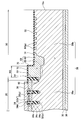
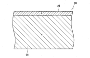
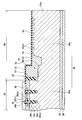
- FIG. 2 is a plan view of the semiconductor device 10.
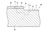
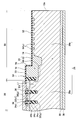
- FIG. 2 is a longitudinal sectional view taken along line II-II in FIG. The expanded sectional view of the outer periphery p-type area
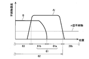
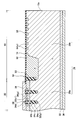
- FIG. 4 is a graph showing an impurity concentration distribution along the line AA in FIG. 3.
- FIG. 6 is an explanatory diagram of a manufacturing process of the semiconductor device 10.
- FIG. 6 is an explanatory diagram of a manufacturing process of the semiconductor device 10.
- FIG. 6 is an explanatory diagram of a manufacturing process of the semiconductor device 10.
- FIG. 6 is an explanatory diagram of a manufacturing process of the semiconductor device 10.
- FIG. 6 is an explanatory diagram of a manufacturing process of the semiconductor device 10.
- FIG. 6 is an explanatory diagram of a manufacturing process of the semiconductor device 10.
- FIG. 6 is an explanatory diagram of a manufacturing process of the semiconductor device 10.
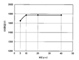
- the graph which shows the relationship between width W3 and DS pressure
- the semiconductor device 10 includes a semiconductor substrate 12 made of SiC (silicon carbide).
- the semiconductor substrate 12 has a MOSFET region 20 and an outer peripheral region 50.
- a MOSFET is formed in the MOSFET region 20.
- the outer peripheral region 50 is a region outside the MOSFET region 20.
- the outer peripheral region 50 is a region between the MOSFET region 20 and the end face 12 a of the semiconductor substrate 12.
- a breakdown voltage structure is formed in the outer peripheral region 50.
- FIG. 1 only the termination trench 54, the boundary p-type region 59, and the guard ring region 64 are shown in the outer peripheral region 50 in consideration of easy viewing.
- a source region 22, a body region 26, a drift region 28, a drain region 30, a p-type floating region 32, a gate trench 34, a source electrode 36, and a drain electrode 38 are formed in the MOSFET region 20. ing.
- a plurality of source regions 22 are formed in the MOSFET region 20.
- the source region 22 is an n-type region containing an n-type impurity at a high concentration.
- the source region 22 is formed in a range exposed on the upper surface of the semiconductor substrate 12.
- the body region 26 is formed on the side and the lower side of the source region 22 and is in contact with the source region 22.
- Body region 26 is a p-type region.
- the body region 26 is exposed on the upper surface of the semiconductor substrate 12 at a position where the source region 22 is not formed.
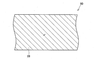
- the drift region 28 is an n-type region containing n-type impurities at a low concentration.
- the n-type impurity concentration of the drift region 28 is lower than the n-type impurity concentration of the source region 22.
- the drift region 28 is formed below the body region 26. The drift region 28 is in contact with the body region 26 and is separated from the source region 22 by the body region 26.
- the drain region 30 is an n-type region containing an n-type impurity at a high concentration.
- the n-type impurity concentration of the drain region 30 is higher than the n-type impurity concentration of the drift region 28.
- the drain region 30 is formed below the drift region 28. Drain region 30 is in contact with drift region 28 and is separated from body region 26 by drift region 28.
- the drain region 30 is formed in a range exposed on the lower surface of the semiconductor substrate 12.
- a plurality of gate trenches 34 are formed in the MOSFET region 20.
- the gate trench 34 is a groove formed on the upper surface of the semiconductor substrate 12.
- Each gate trench 34 is formed so as to penetrate the source region 22 and the body region 26 and reach the drift region 28.
- the plurality of gate trenches 34 extend in parallel to each other.
- a bottom insulating layer 34a, a gate insulating film 34b, and a gate electrode 34c are formed in each gate trench 34.
- the bottom insulating layer 34 a is a thick insulating layer formed at the bottom of the gate trench 34.
- a side surface of the gate trench 34 above the bottom insulating layer 34a is covered with a gate insulating film 34b.
- a gate electrode 34c is formed in the gate trench 34 above the bottom insulating layer 34a.
- the gate electrode 34c is opposed to the source region 22, the body region 26, and the drift region 28 through the gate insulating film 34b.
- the gate electrode 34c is insulated from the semiconductor substrate 12 by the gate insulating film 34b and the bottom insulating layer 34a.
- the upper surface of the gate electrode 34c is covered with an insulating layer 34d.
- the p-type floating region 32 is formed in the semiconductor substrate 12 in a range in contact with the bottom surface (that is, the lower end) of each gate trench 34.
- the periphery of the p-type floating region 32 is surrounded by the drift region 28.
- the p-type floating regions 32 are separated from each other by the drift region 28.
- Each p-type floating region 32 is separated from the body region 26 by the drift region 28.
- the source electrode 36 is formed on the upper surface of the semiconductor substrate 12 in the MOSFET region 20.
- the source electrode 36 is electrically connected to the source region 22 and the body region 26.
- the drain electrode 38 is formed on the lower surface of the semiconductor substrate 12.
- the drain electrode 38 is electrically connected to the drain region 30.
- drift region 28 and drain region 30 extend to the outer peripheral region 50.
- the drift region 28 and the drain region 30 extend to the end face 12 a of the semiconductor substrate 12.
- the drain electrode 38 is formed on the entire lower surface of the semiconductor substrate 12 including the outer peripheral region 50. Further, the upper surface of the semiconductor substrate 12 in the outer peripheral region 50 is covered with an insulating layer 52.
- the drift region 28 in the MOSFET region 20 may be referred to as an element portion drift region 28a
- the drift region 28 in the outer periphery region 50 may be referred to as an outer periphery drift region 28b.
- a stepped portion 70 is formed on the surface of the semiconductor substrate 12 in the outer peripheral region 50.
- the stepped portion 70 divides the surface of the semiconductor substrate 12 into a surface 72 on the central portion side and a surface 74 on the end surface 12a side.
- the surface 72 protrudes upward with respect to the surface 74.
- the thickness of the semiconductor substrate 12 is thicker at the portion corresponding to the surface 72 than at the portion corresponding to the surface 74.
- the MOSFET region 20 described above is formed in a portion corresponding to the surface 72 (a portion having a large thickness).
- the height of the stepped portion 70 is larger than the thickness of the body region 26. Therefore, the front surface 74 is located on the lower side (back surface side) than the lower end of the body region 26.
- a termination trench 54 is formed on the surface 72 of the semiconductor substrate 12 in the outer peripheral region 50.
- An insulating layer 53 is formed in the termination trench 54.
- the termination trench 54 is formed at a position adjacent to the body region 26.
- the termination trench 54 has substantially the same depth as the gate trench 34. Therefore, the insulating layer 53 is in contact with the element portion drift region 28 a at a position deeper than the body region 26.
- the termination trench 54 extends around the MOSFET region 20 when the surface of the semiconductor substrate 12 is viewed in plan. Therefore, body region 26 is separated from any p-type region in outer peripheral region 50 by insulating layer 53. That is, in this embodiment, the region surrounded by the termination trench 54 is the MOSFET region 20.
- a lower end p-type region 60 is formed at a position in contact with the lower end (that is, the bottom surface) of the termination trench 54.
- the lower end p-type region 60 is not formed in the MOSFET region 20.
- an outer peripheral p-type region 62 is formed in a region on the outer peripheral side of the termination trench 54 and in a position in contact with the termination trench 54.
- the outer peripheral p-type region 62 is formed from the position exposed at the surface 72 to the position exposed at the surface 74.
- the outer peripheral p-type region 62 is exposed on the surface 72, the stepped portion 70 and the surface 74.
- the outer peripheral p-type region 62 extends to a position deeper than the lower end of the termination trench 54. As shown in the drawing, in this embodiment, the lower end p-type region 60 and the outer peripheral p-type region 62 are connected. Since the lower end p-type region 60 and the outer peripheral p-type region 62 are one p-type region, hereinafter, these may be collectively referred to as a boundary portion p-type region 59. That is, the boundary p-type region 59 is a p-type region extending across the position exposed at the lower end of the termination trench 54, the position exposed at the surface 72, and the position exposed at the surface 74. As shown in FIG. 1, the boundary p-type region 59 is formed so as to go around the MOSFET region 20 along the termination trench 54. As shown in FIG. 2, an outer peripheral drift region 28 b is formed below the boundary p-type region 59.
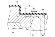
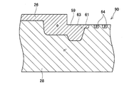
- FIG. 3 shows an enlarged cross-sectional view of the vicinity of the outer peripheral edge of the outer peripheral p-type region 62.
- the outer peripheral p-type region 62 has an Al (aluminum) high concentration region 61 and a B (boron) high concentration region 63.
- the Al high concentration region 61 is a p-type region having a higher Al concentration than B
- the B high concentration region 63 is a p-type region having a higher B concentration than Al.
- the outer peripheral p-type region 62 does not contain p-type impurities other than B and Al except for an uncontrollable error level.
- the Al high concentration region 61 is formed at the outer peripheral end of the outer peripheral p-type region 62 in the range where the outer peripheral p-type region 62 is exposed on the surface 74.
- the B high concentration region 63 is formed in the outer peripheral p-type region 62 other than the Al high concentration region 61. Most of the outer peripheral p-type region 62 is constituted by the B high concentration region 63.
- FIG. 4 shows an impurity concentration distribution (impurity concentration distribution along the line AA in FIG. 3) in the vicinity of the outer peripheral edge of the outer peripheral p-type region 62. 3 and 4, a region 61 a is a region containing Al and not containing B.
- the region 61b contains Al and B, and the concentration of Al is higher than the concentration of B.
- the Al high concentration region 61 is composed of a region 61a and a region 61b.
- the width W1 (that is, the dimension in the direction from the inner circumference side to the outer circumference side) of the Al high concentration region 61 shown in FIG. 3 is wider than each width W2 of the guard ring region 64 described later.
- said width W1, W2 means the dimension in the direction which goes to an outer peripheral side from an inner peripheral side.
- each guard ring region 64 is a p-type region and is formed in a range exposed to the surface 74. Each guard ring region 64 is formed only in a shallow range. Therefore, the lower end of each guard ring region 64 is located on the upper side (surface side) than the lower end of the outer peripheral p-type region 62.
- An outer peripheral drift region 28 b is formed below each guard ring region 64. An outer peripheral drift region 28 b is formed between the guard ring region 64 on the innermost peripheral side (the MOSFET region 20 side) and the outer peripheral p-type region 62.
- the innermost guard ring region 64 is separated from the outer peripheral p-type region 62 by the outer peripheral drift region 28 b. Further, an outer peripheral drift region 28 b is formed between the guard ring regions 64. The guard ring regions 64 are separated from each other by the outer peripheral drift region 28b.
- Each guard ring region 64 contains Al as a p-type impurity. Each guard ring region 64 does not contain p-type impurities other than Al except for an uncontrollable error level.
- the operation of the semiconductor device 10 will be described.
- a voltage that makes the drain electrode 38 positive is applied between the drain electrode 38 and the source electrode 36.
- the gate-on voltage is applied to the gate electrode 34c, whereby the MOSFET in the MOSFET region 20 is turned on. That is, a channel is formed in the body region 26 at a position facing the gate electrode 34 c, and from the source electrode 36 to the drain electrode 38 via the source region 22, the channel, the drift region 28, and the drain region 30. Current flows.
- the application of the gate-on voltage to the gate electrode 34c is stopped, the channel disappears and the MOSFET is turned off.
- the depletion layer extending from the above-described pn junction reaches the boundary p-type region 59 below the termination trench 54 as indicated by an arrow 82 in FIG. Then, a depletion layer spreads from the boundary p-type region 59 into the drift region 28.
- the drift region 28 between the gate trench 34 and the termination trench 54 has a depletion layer extending from the p-type floating region 32 below the gate trench 34 and a boundary p-type region 59 below the termination trench 54 (that is, the lower end p). Depleted by the depletion layer extending from the mold region 60).
- the depth of the gate trench 34 and the depth of the termination trench 54 are substantially equal (that is, the position in the depth direction of the p-type floating region 32 and the position in the depth direction of the lower end p-type region 60).
- equipotential lines extend in the lateral direction (direction parallel to the surface 72). Thereby, electric field concentration in the vicinity of the termination trench 54 is suppressed.
- the boundary p-type region 59 extends from a range in contact with the lower end of the termination trench 54 to a position in contact with the surface 74 of the semiconductor substrate 12. For this reason, in the vicinity of the surface 74, the depletion layer spreads from the boundary p-type region 59 toward the innermost guard ring region 64. When the depletion layer reaches the innermost guard ring region 64, the depletion layer extends from the guard ring region 64 to the adjacent guard ring region 64. In this way, the depletion layer spreads to the outer peripheral side via each guard ring region 64 sequentially. For this reason, the depletion layer extends widely in the outer peripheral region 50. Thereby, a high breakdown voltage in the outer peripheral region 50 is realized.
- the lower boundary p-type region 59 of the termination trench 54 is provided at a deep position like the p-type floating region 32, so that the electric field in the vicinity of the outer peripheral end of the MOSFET region 20 is obtained. Concentration is suppressed. Further, since the boundary p-type region 59 extends from the bottom surface of the termination trench 54 to the surface 74 of the semiconductor substrate 12 on the outer peripheral side of the termination trench 54, the guard ring formed only in a shallow range near the surface 74. A depletion layer can reach the region 64. As a result, extension of the depletion layer in the outer peripheral region 50 is promoted by the plurality of guard ring regions 64. Further, since the guard ring regions 64 are separated from each other, the potential can be distributed relatively evenly in the outer peripheral region 50. For this reason, a high breakdown voltage in the outer peripheral region 50 is realized.
- the Al high concentration region 61 is formed in the outer peripheral end of the outer peripheral p-type region 62 and in the range exposed to the surface 74.
- a method for manufacturing the semiconductor device 10 will be described.
- a semiconductor wafer 90 consisting only of the n-type layer 28 is prepared.
- the n-type layer 28 is a region that becomes the drift region 28.
- a p-type layer 26 is formed on the surface of the n-type layer 28 by epitaxial growth.
- the p-type layer 26 is a region that becomes the body region 26.
- the surface of the semiconductor wafer 90 within a predetermined range is partially etched.
- etching is performed so that the p-type layer 26 is removed and the n-type layer 28 is exposed as shown in FIG.
- a stepped portion 70 is formed on the surface of the semiconductor wafer 90.
- the stepped portion 70 partitions the surface of the semiconductor wafer 90 into a surface 72 and a surface 74.
- B is implanted into a range including the stepped portion 70 on the surface of the semiconductor wafer 90 (that is, a range extending from the surface 72 to the surface 74).
- B is implanted so that B is distributed from a shallow position to a relatively deep position.
- Al is implanted into the range including the outer peripheral end X1 of the implantation range X in the surface 74 of the semiconductor wafer 90 (that is, the implantation range Y in FIG. 8).
- Al is implanted so that Al is implanted only in the vicinity of the surface 74 of the semiconductor wafer 90 by setting the Al implantation energy low.
- ion implantation into the guard ring region 64 is performed. That is, Al is injected into the outer peripheral side (injection range Z corresponding to each guard ring region 64) of the surface 74 of the semiconductor wafer 90 from the injection range Y.
- Al is implanted so that Al is implanted only in the vicinity of the surface 74 of the semiconductor wafer 90 by setting the Al implantation energy low.
- the width of the injection range Z is narrower than the width of the injection range Y.
- the implanted Al and B are diffused and activated.
- a boundary p-type region 59 and a guard ring region 64 are formed.
- the distribution range of B is widened. That is, compared with the implantation range X, the range in which B after diffusion is distributed becomes considerably wide.
- the width of the Al implantation range Y is widened, the Al high concentration region 61 can be easily disposed at the outer peripheral edge of the boundary p-type region 59 even if the B distribution range is expanded. it can.
- the guard ring region 64 is formed at a shallow position near the surface 74 of the semiconductor wafer 90, the guard ring region 64 can be formed with high accuracy.
- Al implanted into the guard ring region 64 has a low diffusion coefficient in SiC, the guard ring region 64 can be formed with higher accuracy. Therefore, the interval between the guard ring regions 64 can be reduced. Furthermore, the interval between the outer peripheral p-type region 62 and the guard ring region 64 can also be reduced.
- the termination trench 54 is formed at the end of the outer peripheral p-type region 62 (the end opposite to the Al high concentration region 61), and the insulating layer 53 is formed in the termination trench 54. To do.
- the structure in the MOSFET region 20 is formed, and other necessary structures (diffusion layer, electrode, insulating layer, etc.) are formed, whereby the semiconductor device 10 of FIG. 1 is completed.
- the order of each process of the manufacturing method mentioned above can be changed suitably.
- the structure in the MOSFET region 20 may be formed before the structure in the outer peripheral region 50 or may be formed in parallel with the structure in the outer peripheral region 50.
- the interval between the guard ring regions 64 can be reduced. Further, the interval between the outer peripheral p-type region 62 and the guard ring region 64 can also be reduced. Therefore, in this semiconductor device 10, the depletion layer tends to extend in the outer peripheral region 50. For this reason, according to this method, the semiconductor device 10 having a high breakdown voltage in the outer peripheral region 50 can be manufactured.
- interval W3 shows the relationship between the interval W3 (see FIG. 2) between the termination trench 54 and the stepped portion 70 and the DS breakdown voltage (drain-source breakdown voltage) of the semiconductor device 10.
- interval W3 is 10 micrometers or more.
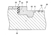
- the lower boundary p-type region 59 (that is, the lower end p-type region 60) of the termination trench 54 is not formed on the MOSFET region 20 side.
- a part of the lower end p-type region 60 may protrude to the MOSFET region 20 side from the termination trench 54.
- the drift region 28 between the gate trench 34 and the termination trench 54 is more easily depleted.
- the protruding portion does not protrude above the lower end of the termination trench 54 (on the body region 26 side).
- the lower end p-type region 60 when a part of the lower end p-type region 60 is located above the lower end depth D1 of the termination trench 54 in the MOSFET region 20 as shown in FIG.
- the distance L1 between them becomes shorter.
- the inter-DS breakdown voltage decreases.
- a part of the lower end p-type region 60 may be disposed above the depth D1, and the distance L1 may be optimized to ensure the withstand voltage between the DSs.
- the stepped portion 70 is formed on the surface of the semiconductor substrate 12, but the surface of the semiconductor substrate 12 may be flat as shown in FIG.
- the body region 26 of the semiconductor device of FIG. 14 is formed by ion implantation. Unlike the epitaxial growth, the ion implantation allows the body region 26 to be formed only in a necessary region on the surface of the semiconductor wafer. Therefore, in the manufacturing process of the semiconductor device of FIG. 14, it is necessary to perform the step of etching part of the p-type layer 26 (body region 26) described in the above-described embodiment (that is, the step of forming the stepped portion 70). There is no. Therefore, in the semiconductor device of FIG. 14, the surface of the semiconductor substrate 12 is flat.
- the lower end p-type region 60 is connected to the outer peripheral p-type region 62.
- the lower end p-type region 60 may be separated from the outer peripheral p-type region 62.
- the outer peripheral p-type region 62 is formed in a shallower range than the termination trench 54. For this reason, the lower end p-type region 60 is separated from the outer peripheral p-type region 62 by the drift region 28.
- the distance L2 between the lower end p-type region 60 and the outer peripheral p-type region 62 is set to a distance at which the depletion layer can extend from the lower end p-type region 60 to the outer peripheral p-type region 62,
- the breakdown voltage of the outer peripheral region 50 can be ensured as in the above-described embodiment.
- the distance L2 is preferably set so as to satisfy the formula of L2 ⁇ ⁇ 2 ⁇ (Vbi ⁇ V) / q ⁇ Nb ⁇ 1/2 .
- ⁇ is a dielectric constant of the drift region 28
- Vbi is a built-in potential between the lower end p-type region 60 and the drift region 28
- V is an applied voltage
- q is an elementary charge
- Nb is This is the n-type impurity concentration of the drift region 28.
- the semiconductor device having the MOSFET has been described.
- another element such as an IGBT may be formed instead of the MOSFET.
- the semiconductor substrate 12 is made of SiC.
- a semiconductor substrate made of another material such as Si may be used.
Landscapes
- Engineering & Computer Science (AREA)
- Physics & Mathematics (AREA)
- Condensed Matter Physics & Semiconductors (AREA)
- General Physics & Mathematics (AREA)
- Manufacturing & Machinery (AREA)
- Computer Hardware Design (AREA)
- Microelectronics & Electronic Packaging (AREA)
- Power Engineering (AREA)
- Electrodes Of Semiconductors (AREA)
Priority Applications (3)
| Application Number | Priority Date | Filing Date | Title |
|---|---|---|---|
| CN201480075197.3A CN105981173B (zh) | 2014-02-10 | 2014-10-06 | 半导体装置以及半导体装置的制造方法 |
| DE112014006350.9T DE112014006350B4 (de) | 2014-02-10 | 2014-10-06 | Halbleitereinrichtungen und Verfahren zum Herstellen einer Halbleitereinrichtung |
| US15/116,288 US9640651B2 (en) | 2014-02-10 | 2014-10-06 | Semiconductor device and method of manufacturing semiconductor device |
Applications Claiming Priority (2)
| Application Number | Priority Date | Filing Date | Title |
|---|---|---|---|
| JP2014023869A JP6231396B2 (ja) | 2014-02-10 | 2014-02-10 | 半導体装置及び半導体装置の製造方法 |
| JP2014-023869 | 2014-02-10 |
Publications (1)
| Publication Number | Publication Date |
|---|---|
| WO2015118721A1 true WO2015118721A1 (ja) | 2015-08-13 |
Family
ID=53777540
Family Applications (1)
| Application Number | Title | Priority Date | Filing Date |
|---|---|---|---|
| PCT/JP2014/076722 Ceased WO2015118721A1 (ja) | 2014-02-10 | 2014-10-06 | 半導体装置及び半導体装置の製造方法 |
Country Status (5)
| Country | Link |
|---|---|
| US (1) | US9640651B2 (enExample) |
| JP (1) | JP6231396B2 (enExample) |
| CN (1) | CN105981173B (enExample) |
| DE (1) | DE112014006350B4 (enExample) |
| WO (1) | WO2015118721A1 (enExample) |
Cited By (1)
| Publication number | Priority date | Publication date | Assignee | Title |
|---|---|---|---|---|
| CN106252390A (zh) * | 2016-09-19 | 2016-12-21 | 西安理工大学 | 一种沟槽‑场限环复合终端结构及其制备方法 |
Families Citing this family (14)
| Publication number | Priority date | Publication date | Assignee | Title |
|---|---|---|---|---|
| JP2018082025A (ja) * | 2016-11-16 | 2018-05-24 | 株式会社 日立パワーデバイス | 半導体装置、電力変換装置及び半導体装置の製造方法 |
| JP6870546B2 (ja) * | 2017-09-14 | 2021-05-12 | 株式会社デンソー | 半導体装置およびその製造方法 |
| CN109346511A (zh) * | 2018-10-15 | 2019-02-15 | 北京工业大学 | 一种应用于功率半导体器件的横向电阻结构 |
| JP7061948B2 (ja) * | 2018-10-23 | 2022-05-02 | 三菱電機株式会社 | 半導体装置、および、半導体装置の製造方法 |
| US11158703B2 (en) * | 2019-06-05 | 2021-10-26 | Microchip Technology Inc. | Space efficient high-voltage termination and process for fabricating same |
| IT201900013416A1 (it) | 2019-07-31 | 2021-01-31 | St Microelectronics Srl | Dispositivo di potenza a bilanciamento di carica e procedimento di fabbricazione del dispositivo di potenza a bilanciamento di carica |
| CN113054011B (zh) * | 2021-02-09 | 2023-06-20 | 杭州士兰集昕微电子有限公司 | 功率半导体器件及其制造方法 |
| JP7697255B2 (ja) * | 2021-04-27 | 2025-06-24 | 富士電機株式会社 | 炭化珪素半導体装置および炭化珪素半導体装置の製造方法 |
| JP7673530B2 (ja) * | 2021-07-09 | 2025-05-09 | 住友電気工業株式会社 | 半導体チップ |
| KR102630457B1 (ko) * | 2022-03-11 | 2024-01-29 | 누보톤 테크놀로지 재팬 가부시키가이샤 | 반도체 장치 |
| WO2023171137A1 (ja) * | 2022-03-11 | 2023-09-14 | ヌヴォトンテクノロジージャパン株式会社 | 半導体装置 |
| JP2023140037A (ja) * | 2022-03-22 | 2023-10-04 | 株式会社東芝 | 半導体装置 |
| TWI832716B (zh) * | 2023-03-02 | 2024-02-11 | 鴻海精密工業股份有限公司 | 製作半導體裝置的方法與半導體裝置 |
| US20250072044A1 (en) * | 2023-08-22 | 2025-02-27 | Wolfspeed, Inc. | Power semiconductor devices having gate trenches with asymmetrically rounded upper and lower trench corners and/or recessed gate electrodes and methods of fabricating such devices |
Citations (3)
| Publication number | Priority date | Publication date | Assignee | Title |
|---|---|---|---|---|
| JPH1187698A (ja) * | 1997-09-02 | 1999-03-30 | Kansai Electric Power Co Inc:The | 高耐圧半導体装置及びこの装置を用いた電力変換器 |
| JP2012004312A (ja) * | 2010-06-16 | 2012-01-05 | Denso Corp | 炭化珪素半導体装置の製造方法および炭化珪素半導体装置 |
| JP2013191734A (ja) * | 2012-03-14 | 2013-09-26 | Toyota Motor Corp | 半導体装置および半導体装置の製造方法 |
Family Cites Families (15)
| Publication number | Priority date | Publication date | Assignee | Title |
|---|---|---|---|---|
| JP3211490B2 (ja) | 1993-06-30 | 2001-09-25 | 株式会社日立製作所 | 半導体装置及びその製造方法 |
| JPH1098188A (ja) * | 1996-08-01 | 1998-04-14 | Kansai Electric Power Co Inc:The | 絶縁ゲート半導体装置 |
| JP4164892B2 (ja) * | 1997-06-30 | 2008-10-15 | 株式会社デンソー | 半導体装置及びその製造方法 |
| US6342709B1 (en) * | 1997-12-10 | 2002-01-29 | The Kansai Electric Power Co., Inc. | Insulated gate semiconductor device |
| JP4538211B2 (ja) * | 2003-10-08 | 2010-09-08 | トヨタ自動車株式会社 | 絶縁ゲート型半導体装置およびその製造方法 |
| JP4915221B2 (ja) | 2006-11-28 | 2012-04-11 | トヨタ自動車株式会社 | 半導体装置 |
| EP2091083A3 (en) * | 2008-02-13 | 2009-10-14 | Denso Corporation | Silicon carbide semiconductor device including a deep layer |
| JP2010147222A (ja) * | 2008-12-18 | 2010-07-01 | Denso Corp | 炭化珪素半導体装置およびその製造方法 |
| JP5396953B2 (ja) | 2009-03-19 | 2014-01-22 | 株式会社デンソー | 炭化珪素半導体装置およびその製造方法 |
| US8372717B2 (en) * | 2009-12-28 | 2013-02-12 | Force Mos Technology Co., Ltd. | Method for manufacturing a super-junction trench MOSFET with resurf stepped oxides and trenched contacts |
| JP5633992B2 (ja) * | 2010-06-11 | 2014-12-03 | トヨタ自動車株式会社 | 半導体装置および半導体装置の製造方法 |
| JP2012054378A (ja) * | 2010-09-01 | 2012-03-15 | Renesas Electronics Corp | 半導体装置 |
| JP5482745B2 (ja) * | 2011-08-10 | 2014-05-07 | 株式会社デンソー | 炭化珪素半導体装置およびその製造方法 |
| JP6277623B2 (ja) * | 2013-08-01 | 2018-02-14 | 住友電気工業株式会社 | ワイドバンドギャップ半導体装置 |
| JP6354525B2 (ja) * | 2014-11-06 | 2018-07-11 | 株式会社デンソー | 炭化珪素半導体装置の製造方法 |
-
2014
- 2014-02-10 JP JP2014023869A patent/JP6231396B2/ja not_active Expired - Fee Related
- 2014-10-06 US US15/116,288 patent/US9640651B2/en not_active Expired - Fee Related
- 2014-10-06 DE DE112014006350.9T patent/DE112014006350B4/de not_active Expired - Fee Related
- 2014-10-06 WO PCT/JP2014/076722 patent/WO2015118721A1/ja not_active Ceased
- 2014-10-06 CN CN201480075197.3A patent/CN105981173B/zh not_active Expired - Fee Related
Patent Citations (3)
| Publication number | Priority date | Publication date | Assignee | Title |
|---|---|---|---|---|
| JPH1187698A (ja) * | 1997-09-02 | 1999-03-30 | Kansai Electric Power Co Inc:The | 高耐圧半導体装置及びこの装置を用いた電力変換器 |
| JP2012004312A (ja) * | 2010-06-16 | 2012-01-05 | Denso Corp | 炭化珪素半導体装置の製造方法および炭化珪素半導体装置 |
| JP2013191734A (ja) * | 2012-03-14 | 2013-09-26 | Toyota Motor Corp | 半導体装置および半導体装置の製造方法 |
Cited By (1)
| Publication number | Priority date | Publication date | Assignee | Title |
|---|---|---|---|---|
| CN106252390A (zh) * | 2016-09-19 | 2016-12-21 | 西安理工大学 | 一种沟槽‑场限环复合终端结构及其制备方法 |
Also Published As
| Publication number | Publication date |
|---|---|
| JP2015153787A (ja) | 2015-08-24 |
| DE112014006350T5 (de) | 2016-10-20 |
| US9640651B2 (en) | 2017-05-02 |
| DE112014006350B4 (de) | 2018-05-09 |
| JP6231396B2 (ja) | 2017-11-15 |
| CN105981173A (zh) | 2016-09-28 |
| US20170012122A1 (en) | 2017-01-12 |
| CN105981173B (zh) | 2019-05-10 |
Similar Documents
| Publication | Publication Date | Title |
|---|---|---|
| JP6231396B2 (ja) | 半導体装置及び半導体装置の製造方法 | |
| JP5196980B2 (ja) | 半導体装置 | |
| US9755042B2 (en) | Insulated gate semiconductor device and method for manufacturing the insulated gate semiconductor device | |
| US9853139B2 (en) | Semiconductor device and method for manufacturing the semiconductor device | |
| JP5136578B2 (ja) | 半導体装置 | |
| US10032866B2 (en) | Semiconductor device and method of manufacturing semiconductor device | |
| JP5758824B2 (ja) | 半導体装置および半導体装置の製造方法 | |
| CN114072922B (zh) | 半导体装置及其制造方法 | |
| WO2011141981A1 (ja) | 半導体装置 | |
| JP6488204B2 (ja) | 半導体装置の製造方法 | |
| CN101964343A (zh) | 半导体装置 | |
| US20110284923A1 (en) | Semiconductor device and manufacturing method of the same | |
| JP2017191817A (ja) | スイッチング素子の製造方法 | |
| JP6391136B2 (ja) | 高電圧ダイオード | |
| CN105280693A (zh) | 半导体装置 | |
| JP5842896B2 (ja) | 半導体装置 | |
| US20150372132A1 (en) | Semiconductor device with composite trench and implant columns | |
| KR20150078449A (ko) | 반도체 소자 및 그 제조 방법 | |
| CN104576730B (zh) | 超级结器件及其制造方法 | |
| KR20130017054A (ko) | 반도체 소자 및 그 제조 방법 | |
| JP2015185656A (ja) | 半導体装置 | |
| JP2014195089A (ja) | 半導体装置 | |
| CN120614850A (zh) | 具有边缘端接区域的半导体电子器件及其制造工艺 | |
| JP2015079987A (ja) | 半導体装置 |
Legal Events
| Date | Code | Title | Description |
|---|---|---|---|
| 121 | Ep: the epo has been informed by wipo that ep was designated in this application |
Ref document number: 14882017 Country of ref document: EP Kind code of ref document: A1 |
|
| WWE | Wipo information: entry into national phase |
Ref document number: 15116288 Country of ref document: US |
|
| WWE | Wipo information: entry into national phase |
Ref document number: 112014006350 Country of ref document: DE |
|
| 122 | Ep: pct application non-entry in european phase |
Ref document number: 14882017 Country of ref document: EP Kind code of ref document: A1 |