WO2015114802A1 - 半導体集積回路装置および電源システム - Google Patents
半導体集積回路装置および電源システム Download PDFInfo
- Publication number
- WO2015114802A1 WO2015114802A1 PCT/JP2014/052286 JP2014052286W WO2015114802A1 WO 2015114802 A1 WO2015114802 A1 WO 2015114802A1 JP 2014052286 W JP2014052286 W JP 2014052286W WO 2015114802 A1 WO2015114802 A1 WO 2015114802A1
- Authority
- WO
- WIPO (PCT)
- Prior art keywords
- voltage
- mosfet
- input electrode
- gate electrode
- integrated circuit
- Prior art date
- Legal status (The legal status is an assumption and is not a legal conclusion. Google has not performed a legal analysis and makes no representation as to the accuracy of the status listed.)
- Ceased
Links
Images


Classifications
-
- H—ELECTRICITY
- H02—GENERATION; CONVERSION OR DISTRIBUTION OF ELECTRIC POWER
- H02M—APPARATUS FOR CONVERSION BETWEEN AC AND AC, BETWEEN AC AND DC, OR BETWEEN DC AND DC, AND FOR USE WITH MAINS OR SIMILAR POWER SUPPLY SYSTEMS; CONVERSION OF DC OR AC INPUT POWER INTO SURGE OUTPUT POWER; CONTROL OR REGULATION THEREOF
- H02M3/00—Conversion of DC power input into DC power output
- H02M3/02—Conversion of DC power input into DC power output without intermediate conversion into AC
- H02M3/04—Conversion of DC power input into DC power output without intermediate conversion into AC by static converters
- H02M3/10—Conversion of DC power input into DC power output without intermediate conversion into AC by static converters using discharge tubes with control electrode or semiconductor devices with control electrode
- H02M3/145—Conversion of DC power input into DC power output without intermediate conversion into AC by static converters using discharge tubes with control electrode or semiconductor devices with control electrode using devices of a triode or transistor type requiring continuous application of a control signal
- H02M3/155—Conversion of DC power input into DC power output without intermediate conversion into AC by static converters using discharge tubes with control electrode or semiconductor devices with control electrode using devices of a triode or transistor type requiring continuous application of a control signal using semiconductor devices only
- H02M3/156—Conversion of DC power input into DC power output without intermediate conversion into AC by static converters using discharge tubes with control electrode or semiconductor devices with control electrode using devices of a triode or transistor type requiring continuous application of a control signal using semiconductor devices only with automatic control of output voltage or current, e.g. switching regulators
- H02M3/158—Conversion of DC power input into DC power output without intermediate conversion into AC by static converters using discharge tubes with control electrode or semiconductor devices with control electrode using devices of a triode or transistor type requiring continuous application of a control signal using semiconductor devices only with automatic control of output voltage or current, e.g. switching regulators including plural semiconductor devices as final control devices for a single load
- H02M3/1588—Conversion of DC power input into DC power output without intermediate conversion into AC by static converters using discharge tubes with control electrode or semiconductor devices with control electrode using devices of a triode or transistor type requiring continuous application of a control signal using semiconductor devices only with automatic control of output voltage or current, e.g. switching regulators including plural semiconductor devices as final control devices for a single load comprising at least one synchronous rectifier element
-
- H—ELECTRICITY
- H02—GENERATION; CONVERSION OR DISTRIBUTION OF ELECTRIC POWER
- H02M—APPARATUS FOR CONVERSION BETWEEN AC AND AC, BETWEEN AC AND DC, OR BETWEEN DC AND DC, AND FOR USE WITH MAINS OR SIMILAR POWER SUPPLY SYSTEMS; CONVERSION OF DC OR AC INPUT POWER INTO SURGE OUTPUT POWER; CONTROL OR REGULATION THEREOF
- H02M1/00—Details of apparatus for conversion
- H02M1/08—Circuits specially adapted for the generation of control voltages for semiconductor devices incorporated in static converters
-
- H—ELECTRICITY
- H03—ELECTRONIC CIRCUITRY
- H03K—PULSE TECHNIQUE
- H03K17/00—Electronic switching or gating, i.e. not by contact-making and –breaking
- H03K17/06—Modifications for ensuring a fully conducting state
- H03K17/063—Modifications for ensuring a fully conducting state in field-effect transistor switches
-
- H—ELECTRICITY
- H02—GENERATION; CONVERSION OR DISTRIBUTION OF ELECTRIC POWER
- H02M—APPARATUS FOR CONVERSION BETWEEN AC AND AC, BETWEEN AC AND DC, OR BETWEEN DC AND DC, AND FOR USE WITH MAINS OR SIMILAR POWER SUPPLY SYSTEMS; CONVERSION OF DC OR AC INPUT POWER INTO SURGE OUTPUT POWER; CONTROL OR REGULATION THEREOF
- H02M1/00—Details of apparatus for conversion
- H02M1/0003—Details of control, feedback or regulation circuits
- H02M1/0009—Devices or circuits for detecting current in a converter
-
- H—ELECTRICITY
- H02—GENERATION; CONVERSION OR DISTRIBUTION OF ELECTRIC POWER
- H02M—APPARATUS FOR CONVERSION BETWEEN AC AND AC, BETWEEN AC AND DC, OR BETWEEN DC AND DC, AND FOR USE WITH MAINS OR SIMILAR POWER SUPPLY SYSTEMS; CONVERSION OF DC OR AC INPUT POWER INTO SURGE OUTPUT POWER; CONTROL OR REGULATION THEREOF
- H02M1/00—Details of apparatus for conversion
- H02M1/0003—Details of control, feedback or regulation circuits
- H02M1/0032—Control circuits allowing low power mode operation, e.g. in standby mode
-
- H—ELECTRICITY
- H02—GENERATION; CONVERSION OR DISTRIBUTION OF ELECTRIC POWER
- H02M—APPARATUS FOR CONVERSION BETWEEN AC AND AC, BETWEEN AC AND DC, OR BETWEEN DC AND DC, AND FOR USE WITH MAINS OR SIMILAR POWER SUPPLY SYSTEMS; CONVERSION OF DC OR AC INPUT POWER INTO SURGE OUTPUT POWER; CONTROL OR REGULATION THEREOF
- H02M1/00—Details of apparatus for conversion
- H02M1/0048—Circuits or arrangements for reducing losses
- H02M1/0054—Transistor switching losses
-
- H—ELECTRICITY
- H03—ELECTRONIC CIRCUITRY
- H03K—PULSE TECHNIQUE
- H03K2217/00—Indexing scheme related to electronic switching or gating, i.e. not by contact-making or -breaking covered by H03K17/00
- H03K2217/0036—Means reducing energy consumption
-
- H—ELECTRICITY
- H10—SEMICONDUCTOR DEVICES; ELECTRIC SOLID-STATE DEVICES NOT OTHERWISE PROVIDED FOR
- H10W—GENERIC PACKAGES, INTERCONNECTIONS, CONNECTORS OR OTHER CONSTRUCTIONAL DETAILS OF DEVICES COVERED BY CLASS H10
- H10W72/00—Interconnections or connectors in packages
- H10W72/90—Bond pads, in general
- H10W72/921—Structures or relative sizes of bond pads
- H10W72/926—Multiple bond pads having different sizes
-
- H—ELECTRICITY
- H10—SEMICONDUCTOR DEVICES; ELECTRIC SOLID-STATE DEVICES NOT OTHERWISE PROVIDED FOR
- H10W—GENERIC PACKAGES, INTERCONNECTIONS, CONNECTORS OR OTHER CONSTRUCTIONAL DETAILS OF DEVICES COVERED BY CLASS H10
- H10W90/00—Package configurations
- H10W90/701—Package configurations characterised by the relative positions of pads or connectors relative to package parts
- H10W90/751—Package configurations characterised by the relative positions of pads or connectors relative to package parts of bond wires
- H10W90/753—Package configurations characterised by the relative positions of pads or connectors relative to package parts of bond wires between laterally-adjacent chips
-
- H—ELECTRICITY
- H10—SEMICONDUCTOR DEVICES; ELECTRIC SOLID-STATE DEVICES NOT OTHERWISE PROVIDED FOR
- H10W—GENERIC PACKAGES, INTERCONNECTIONS, CONNECTORS OR OTHER CONSTRUCTIONAL DETAILS OF DEVICES COVERED BY CLASS H10
- H10W90/00—Package configurations
- H10W90/701—Package configurations characterised by the relative positions of pads or connectors relative to package parts
- H10W90/761—Package configurations characterised by the relative positions of pads or connectors relative to package parts of strap connectors
- H10W90/766—Package configurations characterised by the relative positions of pads or connectors relative to package parts of strap connectors between a chip and a stacked lead frame, conducting package substrate or heat sink
-
- Y—GENERAL TAGGING OF NEW TECHNOLOGICAL DEVELOPMENTS; GENERAL TAGGING OF CROSS-SECTIONAL TECHNOLOGIES SPANNING OVER SEVERAL SECTIONS OF THE IPC; TECHNICAL SUBJECTS COVERED BY FORMER USPC CROSS-REFERENCE ART COLLECTIONS [XRACs] AND DIGESTS
- Y02—TECHNOLOGIES OR APPLICATIONS FOR MITIGATION OR ADAPTATION AGAINST CLIMATE CHANGE
- Y02B—CLIMATE CHANGE MITIGATION TECHNOLOGIES RELATED TO BUILDINGS, e.g. HOUSING, HOUSE APPLIANCES OR RELATED END-USER APPLICATIONS
- Y02B70/00—Technologies for an efficient end-user side electric power management and consumption
- Y02B70/10—Technologies improving the efficiency by using switched-mode power supplies [SMPS], i.e. efficient power electronics conversion e.g. power factor correction or reduction of losses in power supplies or efficient standby modes
Definitions
- the present invention relates to a semiconductor integrated circuit device and a power supply system, for example, a semiconductor integrated circuit device used for converting a voltage and a power supply system using the semiconductor integrated circuit device.
- a power supply system that converts a DC voltage having a predetermined voltage value into a DC voltage having a voltage value different from the predetermined voltage value is known as a so-called DC / DC converter.
- DC / DC converters are used in various electronic devices.
- An example of the electronic device is a computer.
- a power supply voltage supplied to a microprocessor hereinafter referred to as a CPU
- a DC / DC converter is formed by a DC / DC converter.
- a power supply system such as a DC / DC converter has a coil and a plurality of switch elements that periodically change the direction of current flowing through the coil.
- Each of the plurality of switch elements is constituted by a transistor such as a field effect transistor (hereinafter referred to as MOSFET).
- MOSFET field effect transistor
- FIG. 1D shows a MOSFET structure in which a first gate electrode 10 and a second gate electrode 12 are stacked vertically.
- a MOSFET in which a gate electrode 26 (hereinafter referred to as a first gate electrode) and a gate electrode 30 (hereinafter referred to as a second gate electrode) are stacked vertically. The structure of is shown.
- the first gate electrode and the second gate electrode are stacked in the vertical direction, thereby achieving high integration as taught in Patent Document 1, for example. It is possible to reduce the capacitance between the second gate electrode and the drain region of the MOSFET while maintaining it. As a result, the high frequency characteristics of the MOSFET can be improved. By improving the high frequency characteristics, the loss of the DC / DC converter is reduced and the efficiency can be improved. Improvement of the efficiency of the DC / DC converter is an important matter because it leads to reduction of power consumption in an electronic device using the DC / DC converter, for example.
- Patent Documents 1 and 2 were examined.
- Patent Document 1 shows that the first gate electrode of the MOSFET is set to a predetermined positive voltage and an input signal is supplied to the second gate electrode.
- Patent Document 2 shows that the first gate electrode is connected to the source of the MOSFET.
- the inventors of the present application have studied that if the voltage supplied to the first gate electrode is changed to a positive voltage or a negative voltage with respect to the voltage supplied to the source of the MOSFET, the characteristics (on-resistance) of the MOSFET Value, capacity value) was found to change. The present invention has been made based on this finding.
- An object of the present invention is to provide a power supply system capable of improving efficiency and a semiconductor integrated circuit device used therefor.
- a semiconductor integrated circuit device includes a first voltage terminal, a second voltage terminal, an output terminal, a first MOSFET connected between the first voltage terminal and the output terminal, a second voltage terminal, and an output terminal. And a second MOSFET connected between the first and second MOSFETs.
- the first MOSFET has a first input electrode, a drain, and a source
- the second MOSFET is disposed closer to the drain than the first input electrode, the drain, the source, and the first input electrode.
- a second input electrode is disposed closer to the drain than the first input electrode, the drain, the source, and the first input electrode.
- An input signal for complementarily turning on / off the first MOSFET and the second MOSFET is supplied to each first input electrode of the first MOSFET and the second MOSFET. Thereby, a current is alternately supplied from the first voltage terminal and the second voltage terminal to the output terminal.
- the second MOSFET a negative voltage is supplied to the second input electrode disposed on the drain side of the first input electrode with respect to the voltage at the source of the second MOSFET.
- the parasitic capacitance generated between the first input electrode and the drain.
- the first MOSFET and the second MOSFET are complementarily turned on / off, but during the transition time from on to off or off to on, between the first voltage terminal and the second voltage terminal and between the first voltage terminal and the output terminal.
- a current flows between the second voltage terminal and the output terminal.
- the second input electrode and the first input electrode of the second MOSFET are embedded in the stacked first semiconductor region and third semiconductor region, respectively. Formed by layers.
- the first semiconductor region forms the drain of the second MOSFET
- the third semiconductor region forms the source of the second MOSFET.
- the second input electrode is disposed closer to the drain side of the second MOSFET than the first input electrode. Further, since they are stacked, high integration is possible. In this case, a channel of the second MOSFET is generated in the second semiconductor region interposed between the first semiconductor region and the third semiconductor region.
- the semiconductor integrated circuit device selectively supplies a positive voltage and a negative voltage to the second input electrode of the second MOSFET with respect to the voltage at the source of the second MOSFET. It comprises. By supplying a positive voltage with respect to the voltage at the source to the second input electrode of the second MOSFET, it is possible to reduce the on-resistance when the second MOSFET is turned on. By reducing the on-resistance of the second MOSFET, it is possible to reduce the loss in the second MOSFET.
- the loss can be reduced by reducing the transient time and the loss by reducing the on-resistance. It becomes possible to select.
- the selection circuit is supplied with the voltage supplied to the second input electrode in synchronization with the timing at which the second MOSFET is turned on / off according to the input signal supplied to the first input electrode. Select the polarity. Accordingly, it is possible to reduce the loss by reducing the transient time and the loss by reducing the on-resistance in accordance with the on / off of the second MOSFET.
- the semiconductor integrated circuit device includes a detection circuit that detects whether or not the current flowing through the output terminal exceeds a predetermined current value.
- the selection circuit changes the polarity of the voltage supplied to the second input electrode. This makes it possible to select between reducing the loss by reducing the transient time and reducing the loss by reducing the on-resistance according to the value of the load current required by the load coupled to the output terminal. .
- an appropriate voltage polarity for reducing the loss is selected according to the magnitude of the load current. As a result, the loss can be reduced according to the magnitude of the load current.
- the load current changes according to the load state at that time. Therefore, it is possible to select an appropriate means for reducing loss (transient time reduction and on-resistance reduction) according to the load.
- a semiconductor integrated circuit device includes: a first voltage terminal; a second voltage terminal; an output terminal; and a first MOSFET coupled between the first voltage terminal and the output terminal. And a second MOSFET coupled between the output terminal and the second voltage terminal.
- each of the first MOSFET and the second MOSFET includes a first input electrode, a drain, a source, and a second input electrode disposed on the drain side of the first input electrode.
- the first MOSFET and the second MOSFET are complementarily turned on / off by the input signal. By being turned on / off in a complementary manner, current is alternately supplied from the first voltage terminal and the second voltage terminal to the output terminal. The value of the current flowing through the output terminal varies depending on the load current required by the load coupled to the output terminal.
- the semiconductor integrated circuit device further includes a detection circuit that detects a value of a current flowing through the output terminal, and different voltages are applied to the second input electrodes of the first MOSFET and the second MOSFET in response to a detection signal from the detection circuit.
- a supply control circuit is provided.
- the loss is reduced by shortening the transient time in each of the first MOSFET and the second MOSFET, and the loss is reduced or the increase is suppressed by suppressing the on-resistance or suppressing the increase. It will be. As a result, it is possible to reduce the loss of the semiconductor integrated circuit device according to the load, and it is possible to improve the efficiency.
- the control circuit when the current flowing through the output terminal exceeds a predetermined current value, applies a positive voltage to the second gate electrode of each of the first MOSFET and the second MOSFET with respect to the voltage at each source. Supply sex voltage.
- a negative voltage is supplied to the second gate electrode of each of the first MOSFET and the second MOSFET with respect to the voltage at each source.
- the power supply system includes a semiconductor integrated circuit device and a coil element.
- One end of the coil element is coupled to the output terminal of the semiconductor integrated circuit device, and the direction of the current supplied from the output terminal to the coil element changes periodically.
- the semiconductor integrated circuit device has any one of the means (1) to (6) for solving as described above in ⁇ Semiconductor integrated circuit device viewpoint>.
- any of the means (1) to (6) for solving this problem it is possible to reduce the loss of the semiconductor integrated circuit device, so that the loss of the power supply system can be reduced and the efficiency can be improved. Is possible.
- a device for example, a CPU supplied with power by the power supply system is regarded as a load.
- the current demanded by the load (load current) varies depending on the operation status of the device regarded as a load.
- the ratio between the loss caused by the transient time and the loss caused by the on-resistance in the loss in the semiconductor integrated circuit device is heavy (heavy load), and the load current It was found that the load was different from that when the load was light (light load) and the load current was relatively low. According to the study of the present inventor, as the load current increases, the ratio of loss generated by the on-resistance increases.
- the load current is detected by the detection circuit, and in response to the detection signal, the selection circuit (means (5)) or the control circuit (means (6))
- the voltage supplied to the second input electrode of the MOSFET (the second MOSFET in the means (5), the first MOSFET and the second MOSFET in the means (6)) is selected.
- the selection circuit or the control circuit selects a voltage having a polarity such that the voltage supplied to the second input electrode of the MOSFET is more positive than the voltage at the source of the MOSFET. This reduces the loss that occurs during heavy loads.
- the selection circuit or the control circuit selects a voltage having a polarity that is more negative than the voltage at the source of the MOSFET and supplies it to the second input electrode of the MOSFET. Thereby, the loss at the time of light load is reduced.
- the loss can be reduced by items that are effective for reduction (loss reduction by shortening the transient time, loss reduction by reducing on-resistance). As a result, it is possible to reduce the loss of the power supply system according to the load.
- the above-described first input electrode corresponds to, for example, the second gate electrode of Patent Document 1
- the above-described second input electrode corresponds to the first gate electrode.
- the loss in the transient time is also referred to as switching loss
- the loss due to the on-resistance is also referred to as conduction loss.
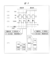
- FIG. 10 is a block diagram showing a main configuration of a semiconductor integrated circuit device according to a third embodiment.
- A) And (B) is a wave form diagram which shows operation
- FIG. 10 is a block diagram showing a configuration of a main part of a semiconductor integrated circuit device according to a fourth embodiment.
- (A) to (D) are waveform diagrams showing the operation of the semiconductor integrated circuit device according to the fourth embodiment.
- (A) to (F) are explanatory diagrams for explaining the operation of the semiconductor integrated circuit device according to the fourth embodiment.
- FIG. 10 is a characteristic diagram illustrating characteristics of the semiconductor integrated circuit device according to the fourth embodiment.
- (A) to (F) are explanatory diagrams for explaining the operation of the semiconductor integrated circuit device according to the first embodiment.
- (A) to (F) are explanatory diagrams for explaining the operation of the semiconductor integrated circuit device according to the first embodiment.
- 4 is a characteristic diagram showing characteristics of the semiconductor integrated circuit device according to the first embodiment.
- FIG. 10 is a characteristic diagram illustrating characteristics of the semiconductor integrated circuit device according to the second embodiment.
- (A) And (B) is the block diagram and waveform diagram which show the principal part structure of the semiconductor integrated circuit device concerning Embodiment 5.
- FIG. (A) to (E) are explanatory diagrams for explaining the operation of the semiconductor integrated circuit device according to the fifth embodiment.
- FIG. 10 is a characteristic diagram illustrating characteristics of the semiconductor integrated circuit device according to the fifth embodiment.
- (A) And (B) is a principal part structure and operation
- FIG. 20 is a characteristic diagram illustrating characteristics of the semiconductor integrated circuit device according to the sixth embodiment.
- (A) And (B) is the block diagram and waveform diagram which show the principal part structure of the semiconductor integrated circuit device concerning Embodiment 7.
- FIG. (A) to (E) are explanatory diagrams for explaining the operation of the semiconductor integrated circuit device according to the seventh embodiment.
- FIG. 20 is a characteristic diagram illustrating characteristics of the semiconductor integrated circuit device according to the seventh embodiment.
- FIG. 10 is a waveform diagram showing waveforms of main parts of a semiconductor integrated circuit device according to an eighth embodiment.
- FIG. 20 is a characteristic diagram illustrating characteristics of the semiconductor integrated circuit device according to the eighth embodiment.
- FIG. 10 is a block diagram illustrating a configuration of a semiconductor integrated circuit device according to a ninth embodiment.
- FIG. 29 is a block diagram showing a second modification of the semiconductor integrated circuit device according to the ninth embodiment.
- FIG. 29 is a block diagram showing a third modification of the semiconductor integrated circuit device according to the ninth embodiment.
- FIG. 10 is a block diagram showing a configuration of a semiconductor integrated circuit device according to a tenth embodiment.
- FIG. 20 is a circuit diagram showing a configuration of a main part of a semiconductor integrated circuit device according to a tenth embodiment.
- (A) to (E) are waveform diagrams showing the operation of the semiconductor integrated circuit device according to the tenth embodiment.
- FIG. 20 is a block diagram showing a configuration of a semiconductor integrated circuit device according to an eleventh embodiment.
- FIG. 20 is a circuit diagram showing a configuration of main parts of a semiconductor integrated circuit device according to an eleventh embodiment.
- (A) to (E) are waveform diagrams showing the operation of the semiconductor integrated circuit device according to the eleventh embodiment.
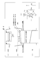
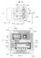
- (A) And (B) is the schematic diagram and top view which show the relationship between a semiconductor integrated circuit device, a package, and a power supply system.
- A) And (B) is the top view and sectional drawing of MOSFET which have a 1st gate electrode and a 2nd gate electrode. It is explanatory drawing for demonstrating the loss of a semiconductor integrated circuit device.
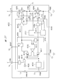
- FIG. 1 is a block diagram showing a configuration of a semiconductor integrated circuit device and a power supply system according to an embodiment.
- (A) to (G) are waveform diagrams showing the operation of the semiconductor integrated circuit device according to the embodiment.
- FIG. 40 is a block diagram showing the configuration of the power supply system.
- reference numeral 4000 denotes a power supply system
- reference numeral 4001 denotes a load coupled to the power supply system 4000. Since the load 4001 can be regarded as a current source equivalently, the load 4001 is shown as a symbol of a current source in the figure, but as described above, for example, the CPU corresponds to the load.
- the power supply system 4000 is not particularly limited, but includes a control semiconductor integrated circuit device 4007, a coil element 4008, a smoothing capacitor 4008, a boot capacitor 4009, and a plurality of semiconductor chips 4004 to 4006 sealed in one package 4002. It has.
- the plurality of semiconductor chips sealed in one package 4002 are a high-side MOSFET 4005, a low-side MOSFET 4006, a high-side MOSFET 4005, and a driver 4003 that drives the low-side MOSFET 4006. That is, the high-side MOSFET 4005, the low-side MOSFET 4006, and the driver 4003 are formed on separate semiconductor chips. These three semiconductor chips will be described later with reference to FIGS. 36A and 36B, but are sealed in one package. Since the package is mounted as a unit on, for example, a printed circuit board, the package 4002 is referred to as a semiconductor integrated circuit device in this specification. Therefore, in the following description, 4002 is described as a semiconductor integrated circuit device.
- the voltage supplied to the drain of the MOSFET 4005 has a higher potential than the voltage supplied to the source of the MOSFET 4006. Therefore, the MOSFET 4005 is referred to as a high side MOSFET, and the MOSFET 4006 is referred to as a low side MOSFET.
- each of T1 to T6 is a terminal provided in the semiconductor integrated circuit device 4002.
- the semiconductor integrated circuit device 4002 is provided with a plurality of terminals. In FIG. 40, only main terminals are shown as terminals T1 to T6. For example, a terminal to which an input signal from the control semiconductor integrated circuit device 4007 is transmitted is omitted in FIG.
- the terminal T1 is an output terminal that outputs the output signal VSWH of the semiconductor integrated circuit device 4002
- the terminal T2 is a voltage terminal that supplies the ground voltage PGND to the low-side MOSFET 4006, and the terminal T3 is a voltage terminal that supplies the ground voltage CGND to the driver. is there.
- the terminal T4 is a voltage terminal for supplying the power supply voltage VCIN to the control circuit 4004.
- the terminal T5 is a voltage terminal for supplying the power supply voltage BOOT corresponding to the voltage of the output signal VSWH to the driver.
- the terminal T6 is connected to the high side MOSFET 4005. A voltage terminal for supplying the input voltage VIN.
- each of the high-side MOSFET 4005 and the low-side MOSFET 4006 is an N-channel MOSFET, and will be described later with reference to FIGS. 37A and 37B. It has a first gate electrode G1, a second gate electrode G2 corresponding to a second input electrode, a source S and a drain D.
- the second input electrode (second gate electrode) G2 is disposed closer to the drain D than the first input electrode (first gate electrode) G1, and the MOSFET is arranged according to the voltage supplied to the first gate electrode G1. Turn on or off (on / off).
- the second input electrode (second gate electrode) G2 of each of the high-side MOSFET 4005 and the low-side MOSFET 4006 has a positive polarity voltage or A negative polarity voltage is supplied.
- FIG. 40 in the high-side MOSFET 4005 and the low-side MOSFET 4006, a parasitic diode formed between the semiconductor region where these MOSFETs are formed and the semiconductor region corresponding to the drain is shown as DD.
- the back gates of these MOSFETs are connected to the source. Since the connection destination of the second gate electrode G2 of each of the high-side MOSFET 4005 and the low-side MOSFET 4006 will be described later in each embodiment, the connection destination of the second gate electrode G2 is not clearly shown in FIG.
- the high-side MOSFET 4005 has a source / drain path connected in series between the voltage terminal T6 and the output terminal T1, and the first gate electrode G1 is connected to the output terminal T7 of the driver 4003.
- the low-side MOSFET 4006 has a source / drain path connected in series between the output terminal T1 and the voltage terminal T2, and the first gate electrode G1 is connected to the output terminal T9 of the driver 4003.
- the ground voltage PGND is supplied to the voltage terminal T2
- a positive voltage higher than the ground voltage PGND is supplied to the voltage terminal T6 as the input voltage VIN. Therefore, here, it is assumed that the drain D of the high-side MOSFET 4005 is connected to the voltage terminal T6 and the source S is connected to the output terminal T1. Similarly, it is assumed that the drain D of the low-side MOSFET 4006 is connected to the output terminal T1, and the source S is connected to the voltage terminal T2.
- the high side MOSFET 4005 receives the output signal (drive signal) GH output from the output terminal T7 of the driver 4003 as an input signal at the first gate electrode G1. Further, the low-side MOSFET 4006 receives the output signal (drive signal) GL output from the output terminal T9 of the driver 4003 as an input signal at the first gate electrode G1.
- the driver 4003 changes the voltages of the drive signals GH and GL so that the high-side MOSFET 4005 and the low-side MOSFET 4006 are turned on / off complementarily.
- the high-side MOSFET 4005 and the low-side MOSFET 4006 are complementarily turned on / off by the drive signals GH and GL, and accordingly, the voltage terminal VIN or the via the source / drain path of the high-side MOSFET 4005 or the low-side MOSFET 4006.
- the voltage terminal PGND is electrically connected to the output terminal T1.
- the voltage formed at one end of the coil element 4008 is supplied to the boot capacitor element 4010.
- the boot capacitive element 4010 forms a voltage BOOT having a voltage value higher than the voltage value at the output terminal T1 by periodically changing the voltage at one end of the coil element 4008, and supplies the voltage BOOT to the voltage terminal T5.
- the driver 4003 includes drive circuits 4011 and 4012 and a control circuit 4004.
- the drive circuit 4011 uses the voltage from the voltage terminal T8 as a reference voltage, the voltage BOOT from the voltage terminal T5 as a power supply voltage, and outputs a signal according to the output signal f from the control circuit 4004 as the drive signal GH.
- the drive circuit 4011 drives the drive signal GH based on the voltage at the source S of the high-side MOSFET 4005, in other words, the voltage at the output terminal T1. Is output. Therefore, the voltage of the drive signal GH changes between, for example, a reference voltage (voltage at the voltage terminal T8) and the voltage BOOT.
- the drive circuit 4012 operates using the voltage at the voltage terminal T10 as a reference voltage and the power supply voltage VCIN supplied to the voltage terminal T4 as a power supply voltage.
- the drive circuit 4012 uses the ground voltage PGND and the voltage VCIN as power supply voltages, and outputs the drive signal GL according to the output signal c from the control circuit 4004. Output to the first gate electrode G1 of the low-side MOSFET 4006 via the output terminal T9.
- the control circuit 4004 operates using the ground voltage CGND supplied to the voltage terminal T3, the voltage VCIN supplied to the voltage terminal T4, and the voltage BOOT supplied to the voltage terminal T5 as operation power supplies.
- the control circuit 4004 has control terminals T11 and T12, and forms output signals f and c according to a pulse width control signal PWM (input signal a) supplied from the control semiconductor integrated circuit device 4007 to the control terminal T11. .
- a control signal DISBL # for instructing whether or not to operate the control circuit 4004 is supplied to the control terminal T12.
- the power supply voltage VCIN is supplied to the control terminal T12 via the resistance element 4022.
- the control circuit 4004 Since the power supply voltage VCIN is at a high level, the control signal DISBL # is at a high level, and the control circuit 4004 forms output signals g and c according to the pulse width control signal PWM supplied to the control terminal T11. On the other hand, when the control signal DISBL # is set to the low level, the control circuit 4004 enters a non-operating state. Thereby, the power supply system 4000 can be controlled to be in an operating state or a non-operating state by the control signal DISBL #.
- the ground voltage CGND supplied to the voltage terminal T3 of the control circuit 4004 is substantially the same voltage (ground voltage GND) as the ground voltage PGND supplied to the voltage terminal T2 connected to the source S of the low-side MOSFET 4006.
- the low-side MOSFET 4006 operates by electrically separating the voltage terminal T3 that supplies the ground voltage to the control circuit 4004 and the voltage terminal T2 that supplies the ground voltage to the source S of the low-side MOSFET 4006. It is possible to prevent the fluctuation of the ground voltage PGND caused by this from being transmitted to the control circuit 4004.
- the voltage value of the voltage BOOT supplied to the voltage terminal T5 is set higher than the power supply voltage VCIN supplied to the voltage terminal T4.
- the control circuit 4004 is configured such that the high level of the output signal f of the control circuit 4004 becomes the voltage BOOT. As a result, the output signal f having the voltage BOOT that is higher than the power supply voltage VCIN is input to the drive circuit 4011.
- the input voltage VIN is, for example, 12V
- the power supply voltage VCIN for the driver 4003 is, for example, 5V.
- each of the drive circuits 4011 and 4012 functions as a buffer circuit. Therefore, the drive circuit 4012 supplies the output signal c from the control circuit 4004 to the first gate electrode G1 of the low-side MOSFET 4006.
- the voltage of the drive signal GL supplied to the first gate electrode G1 of the low-side MOSFET 4006 transitions between the power supply voltage VCIN and the ground voltage.
- the drive circuit 4011 supplies the output signal f from the control circuit 4004 to the first gate electrode G1 of the high-side MOSFET 4005.
- the drive circuit 4011 is supplied with the voltage BOOT as the power supply voltage, and the high level voltage of the output signal f becomes the voltage BOOT. Therefore, the voltage of the drive signal GH supplied to the first gate electrode G1 of the high side MOSFET 4005 transitions between the voltage BOOT and the voltage VSWH at the voltage terminal T8 (voltage at the source of the high side MOSFET).
- loss due to the threshold voltage of the high side MOSFET 4005 is reduced.
- the output voltage Vout output from the output terminal T13 of the power supply system 4000 is supplied to the control semiconductor integrated circuit device 4007.
- the control semiconductor integrated circuit device 4007 forms a pulse width control signal PWM (input signal a) according to the voltage value of the output voltage Vout. That is, the pulse width control signal PWM having a pulse width (for example, a period during which the output voltage Vout is high) is formed.
- the control circuit 4004 in this embodiment includes level shifters 4013 and 4014, an input logic circuit 4018, AND circuits 4016 and 4017, a NOR circuit 4014, an inverter circuit 4020, a low voltage detection circuit 4021, and an overlap prevention circuit 4015.
- the voltage BOOT described above is supplied to the level shifter 4013, and the high level of the output signal f output from the level shifter 4013 is set to the voltage value of the voltage BOOT.
- the overlap prevention circuit 4015 is provided with a voltage conversion circuit that converts the high-level voltage value of the output signal f into an appropriate value.
- the AND circuit 4016 is a three-input AND circuit having one inverting input terminal and two non-inverting input terminals
- the AND circuit 4017 has two inverting input terminals and one non-inverting input terminal. It is a 3-input AND circuit having an inverting input terminal.
- the inverting input terminal is a terminal that inverts the signal supplied to the terminal and supplies it to the AND circuit
- the non-inverting terminal is a terminal that supplies the signal supplied to the terminal as it is to the AND circuit.
- inverter 4020 has a hysteresis function in order to prevent malfunction due to noise.
- the input logic circuit 4018 has a plurality of functions, but description thereof is omitted here.
- the pulse width control signal PWM (input signal a) output from the control semiconductor integrated circuit device 4007 is input to the input logic circuit 4018 via the control terminal T11.
- the output signal b of the input logic circuit 4018 is supplied to the inverting input terminal of the AND circuit 4017 and the non-inverting input terminal of the AND circuit 4016.
- the output signals of the NOR circuit 4019 are supplied to the non-inverting input terminals of the AND circuits 4016 and 4017, respectively.
- a control signal DISBL # is supplied to one input terminal of the NOR circuit 4019 via an inverter 4019, and a power supply voltage VCIN is supplied to the other input terminal via a low voltage detection circuit 4021.
- the power supply voltage VCIN is input to the low voltage detection circuit 4021.
- a high level output signal is formed and supplied to the NOR circuit 4019.
- the NOR circuit 4019 forms a low level output signal.
- each of the AND circuits 4016 and 4017 transmits the output signal b of the input logic circuit 4018 and / or the output signals d and g of the overlap prevention circuit 4015 to its output. No longer. As a result, the control circuit 4004 becomes inoperative.
- each of the AND circuits 4016 and 4017 transmits the output signal b of the input logic circuit 4018 and / or the output signals d and g of the overlap prevention circuit 4015 to its output, and the control circuit 4004 It becomes an operation state.
- the output signal d of the overlap prevention circuit 4015 is supplied to the inverting input terminal of the AND circuit 4016, and the output signal g of the overlap prevention circuit 4015 is supplied to the inverting input terminal of the AND circuit 4017.
- the output signal e of the AND circuit 4016 is input to the drive circuit 4011 as the output signal f of the control circuit 4004 via the level shifter 4013.
- the output signal f is input to the overlap prevention circuit 4015.
- the output signal c of the AND circuit 4017 is input to the drive circuit 4012 as an output signal of the control circuit 4004.
- the output signal c is level-shifted to a desired voltage value by the level shifter 4014 and supplied to the overlap prevention circuit 4015.
- the overlap prevention circuit 4015 is a circuit for preventing the high-side MOSFET 4005 and the low-side MOSFET 4006 from being turned on simultaneously. At the same time, in order to prevent the on-state from being turned on, the output signals c and f are received, and the high levels of the output signals d and g that do not overlap in time are formed.
- Such a circuit can be configured by using a plurality of logic circuits and delay circuits, for example.
- 41 (A) to 41 (G) are waveform diagrams of the signals (output signals and control signals) a to g described above.
- the horizontal axis indicates time
- the vertical axis indicates voltage.
- FIG. 41A is a waveform diagram of a pulse width control signal PWM (denoted as a in the figure) output from the control semiconductor integrated circuit device 4007.
- PWM pulse width control signal
- FIG. 41A is a waveform diagram of a pulse width control signal PWM (denoted as a in the figure) output from the control semiconductor integrated circuit device 4007.
- the control semiconductor integrated circuit device 4007 changes the pulse width (high-level period) in the pulse width control signal PWM, and outputs the output voltage. Control is performed so that the voltage value of Vout becomes a predetermined value.
- a so-called PWM control method is employed.
- the pulse width control signal PWM (a) changes from the low level to the high level at time t1.
- the input logic circuit 4018 changes the output signal b from the low level to the high level at time t2 after a predetermined delay time (FIG. 41B).
- the AND circuit 4017 changes the output signal c to low level at time t2 when the output signal b supplied to the inverting input terminal changes to high level (FIG. 41C).
- the drive circuit 4012 forms the low-level drive signal GL and supplies it to the first gate electrode G1 of the low-side MOSFET 4006.
- the drive circuit 4012 functions as a buffer, the drive signal GL and the output signal c are synchronized with each other. Therefore, it can be considered that the waveform of the drive signal GL is shown in FIG. 41C, and in FIG. 41C, the reference sign GL meaning the drive signal GL is shown as (GL). ing.
- the overlap prevention circuit 4015 receives a change (change from high level to low level) of the output signal c via the level shifter 4014. When this change is received, at time t3 after a predetermined delay time, the overlap prevention circuit 4015 changes the output signal d from the high level to the low level (FIG. 41D). Since the output signal d is supplied to the inverting input terminal of the AND circuit 4016, when the output signal d changes to the low level, the AND circuit 4016 changes the output signal e from the low level to the high level at time t3. (FIG. 41E).
- the level shifter 4013 In response to the change of the output signal e of the AND circuit 4016 from the low level to the high level, the level shifter 4013 forms the high-level output signal f. Since the voltage BOOT is supplied as the operating voltage to the level shifter 4013, the high level of the output signal f becomes the voltage value of the voltage BOOT. This output signal f is supplied to the first gate electrode G1 of the high-side MOSFET 4005 through the drive circuit 4011 that functions as a buffer. The drive circuit 4011 uses the voltage BOOT and the voltage VSWH at the voltage terminal T8 as operating voltages.
- the high level voltage value of the drive signal GH supplied from the drive circuit 4011 to the first gate electrode G1 of the high side MOSFET 4005 is the voltage BOOT
- the low level voltage value of the drive signal GH is the voltage VSWH. Since the output signal f and the drive signal GH are synchronized, FIG. 41 (F) shows that the output signal f and the output signal GH change to high level (voltage BOOT) at time t4. Yes.
- the overlap prevention circuit 4015 changes the output signal g from low level to high level at time t5 after a predetermined time (FIG. 41 (G)).
- the drive signal GL of the drive circuit 4012 changes from the high level to the low level at time t2.
- the drive signal GH of the drive circuit 4011 changes from the low level (VSWH) to the high level (BOOT). Accordingly, at time t2, the low-side MOSFET 4006 starts to transition to the off state, and at time t4, the high-side MOSFET 4005 starts to transition to the on state.
- the input voltage VIN is supplied to the output terminal T1 through the high-side MOSFET 4005, and is supplied to one end of the coil element 4008 and one end of the boot capacitor 4010.
- a current is supplied from the voltage terminal T6 to one end of the coil element 4008 via the output terminal T1.
- the pulse width control signal PWM (a in FIG. 41A) changes from the high level to the low level (FIG. 41A).
- the input logic circuit 4018 changes the output signal b from the high level to the low level at time t7 after a predetermined time (FIG. 41 (b)).
- the output signal e of the AND circuit 4016 changes to the low level at time t7 (FIG. 41 (e)).
- the level shifter 4013 changes the output signal f from the high level (voltage BOOT) to the low level.
- the drive circuit 4011 changes the drive signal GH from the high level (BOOT) to the low level (VSWH) (time t8 in FIG. 41F).
- the overlap prevention circuit 4015 changes the output signal g from the high level to the low level at time t9 after a predetermined time in response to the change to the low level ( FIG. 41 (G)).
- the low level is supplied to the two inverting input terminals of the AND circuit 4017, and the output signal c of the AND circuit 4017 changes from the low level to the high level (time t9 in FIG. 41C). ).
- This output signal c is buffered by the drive circuit 4012 and supplied to the first gate electrode G1 of the low-side MOSFET 4006 as the drive signal GL.
- the overlap prevention circuit 4015 changes the output signal d from the low level to the high level after a lapse of a predetermined time after the output signal c changes to the high level. (Time t10 in FIG. 41D).
- the drive signal GH supplied to the first gate electrode G1 of the high-side MOSFET 4005 transitions to the low level (VSWH), and at time t9 after time t8, the first gate of the low-side MOSFET 4006.
- the drive signal GL supplied to the electrode G1 transitions to a low level. That is, it is possible to prevent a period in which the high-side MOSFET 4005 and the low-side MOSFET 4006 are turned on at the same time.
- the low-side MOSFET 4006 transitions to the on state.
- the output terminal T1 is connected to the voltage terminal T2 via the low-side MOSFET 4006.
- a current flows from one end of the coil element 4008 toward the voltage terminal T2 via the output terminal T1.
- the control semiconductor integrated circuit device 4007 controls the pulse width of the pulse width control signal PWM according to the voltage value of the output voltage Vout so that the generated voltage value of the output voltage Vout becomes a predetermined value.
- FIG. 37A is a schematic plan view showing the layout of the low-side MOSFET 4006 in the semiconductor chip.
- FIG. 37B is a schematic cross-sectional view showing a cross section of the low-side MOSFET 4006 when viewed along B-B ′ in FIG.
- reference numeral 3700 denotes a semiconductor chip.
- two MOSFETs are formed in the semiconductor chip 3700, and the source S, drain D, first gate electrode G1, and second gate electrode G2 of each of the two MOSFETs are formed. Are connected to each other to form one low-side MOSFET 4006.
- 3701 is the source electrode of each of the two MOSFETs
- 3702 is the second gate electrode G2, 3703 of each of the two MOSFETs
- the drain electrode of the low-side MOSFET 4006 is the back surface of the semiconductor chip 3700.
- the source electrode 3701 is formed so as to cover a part of the second gate electrode 3702.
- the drive signal GL is supplied to the second gate electrode 3702 using the region of the second gate electrode 3702 that is not covered with the source electrode 3702.
- reference numeral 3704 denotes an N ⁇ type (first conductivity type) semiconductor region which functions as the drain D of the low-side MOSFET 4006.
- Reference numeral 3705 denotes a P ⁇ -type (second conductivity type) semiconductor region, which is a semiconductor region where a MOSFET channel is formed.
- Reference numeral 3706 denotes an N + type (first conductivity type) semiconductor region which functions as the source S of the MOSFET.
- a semiconductor region 3705 is stacked on the main surface of the semiconductor region 3704, and a semiconductor region 3706 is stacked on the main surface of the semiconductor region 3705. As shown in the figure, grooves are formed in the semiconductor regions 3704, 3705 and 3706.
- a metal layer 3708 is formed in the groove of the semiconductor region 3704 with the insulating layer 3707 interposed therebetween.
- a metal layer 3709 is formed in the trenches of the semiconductor regions 3704 and 3705 with the insulating layer 3707 interposed therebetween so as to overlap with the metal layer 3708.
- the metal layer 3709 constitutes the first gate electrode G1 described above, and the metal layer 3708 constitutes the second gate electrode G2 described above.
- the part of the insulating layer 3707 sandwiched between the metal layer 3709 functioning as the first gate electrode G1 and the semiconductor region 3705 can be understood as a gate insulating film of the low-side MOSFET 4006.
- the metal layer 3709 constituting the first gate electrode G1 overlaps with the semiconductor region 3706 functioning as the source S and the semiconductor region 3704 functioning as the drain D in the vertical direction of the groove.
- the metal layer 3708 functioning as the second gate electrode G2 is embedded in the semiconductor region 3704 functioning as the drain D in the vertical direction of the trench. In other words, the second gate electrode G2 is disposed closer to the drain D than the first gate electrode G1 in the longitudinal direction of the trench.
- reference numeral 3701 denotes a source electrode, which is electrically connected to a semiconductor region 3706 functioning as a source S. Note that the source electrode 3701 is also electrically connected to a semiconductor region 3705 where a channel is formed. As a result, the source S and the back gate of the low-side MOSFET 4006 are electrically connected to the source electrode 3701.
- the metal layer 3709 functioning as the first gate electrode G1 is connected to the connection pad 3703 shown in FIG.
- Reference numeral 3710 denotes a drain electrode provided on the back surface of the semiconductor chip 3700.
- Crss indicates the first gate-drain capacitance that is formed between the first gate electrode G1 and the drain D.
- the high-side MOSFET 4005 it is possible to reduce the capacitance Crss between the first gate and the drain by changing the polarity of the voltage supplied to the second gate electrode G2 (based on the voltage at the source). In addition, the on-resistance can be reduced.
- the low-side MOSFET 4006 (FIG. 40) is larger in size than the high-side MOSFET 4005 in order to flow the current from the coil element 4008 to the ground voltage PGND and lower the voltage at the output terminal T1. Has been increased. Therefore, reduction of the first gate-drain capacitance Crss and the on-resistance in the low-side MOSFET 4006 is particularly effective.
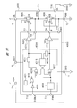
- FIG. 1A is a circuit diagram showing a configuration of a main part of the semiconductor integrated circuit device 4002 according to the first embodiment.
- FIG. 1B is a waveform diagram showing voltage waveforms in the semiconductor integrated circuit device 4002 shown in FIG.
- FIG. 1A shows a low-side MOSFET 4006 and a drive circuit 4012 in the semiconductor integrated circuit device 4002 shown in FIG.
- a portion not shown in FIG. 1A has the same configuration as that of the semiconductor integrated circuit device 4002 shown in FIG.
- the first gate electrode G1 of the low-side MOSFET 4006 is connected to the output terminal T9 of the driver 4003, its source and back gate are connected to the voltage terminal T2, and its drain is the semiconductor integrated circuit device 4002. Are connected to the output terminal T1.
- the driver 4003 includes a drive circuit 4012 that drives the low-side MOSFET 4006, and a drive signal GL from the drive circuit is supplied to the first gate electrode G1 of the low-side MOSFET 4006 via the output terminal T9.
- the driver 4003 includes a control terminal T14 and a second gate electrode control circuit 1001 connected to the control terminal T14.
- the control terminal T14 is connected to the second gate electrode G2 of the low-side MOSFET 4006, and the second gate control signal UL formed by the second gate electrode control circuit 1001 is supplied to the second gate electrode of the low-side MOSFET 4006 via the control terminal T14. Supplied to G2.
- the second gate electrode control circuit 1001 includes a variable voltage source 1004 as an example in FIG.
- Variable voltage source 1004 generates a positive voltage with respect to ground voltage CGND.
- the generated voltage value is variable.
- the ground voltage CGND is the ground voltage GND substantially the same as the ground voltage PGND. Therefore, the second gate electrode control circuit 1001 forms a second gate control signal UL that has a positive polarity with respect to the source of the low-side MOSFET 4006 and changes its voltage value.
- FIG. 1C is a circuit diagram showing an example of the second gate electrode control circuit 1000 that forms the second gate control signal UL having a positive voltage.
- FIG. 1D is a circuit diagram showing an example of the second gate electrode control circuit 1000 that forms the second gate control signal UL having a negative voltage.
- FIG. 1B is a waveform diagram showing a voltage waveform of the second gate control signal UL formed by the second gate electrode control circuit 1000 shown in FIG.
- a positive voltage means a positive voltage
- a negative voltage means a negative voltage.
- reference numeral 1002 denotes an N-channel MOSFET
- reference numerals 1003 and 1004 denote resistance elements
- reference numeral 1005 denotes a differential amplifier circuit
- reference numeral 1006 denotes a variable voltage source.
- Resistance elements 1003 and 1004 are connected in series between the control terminal T14 and the ground voltage CGND, and a divided voltage is taken out from a connection node between the resistance elements 1003 and 1004.
- the extracted divided voltage is supplied to the inverting input ( ⁇ ) of the differential amplifier circuit 1005, and the variable voltage from the variable voltage source 1006 is supplied to the non-inverting input (+) of the differential amplifier circuit 1005. .
- the output signal of the differential amplifier circuit 1005 is supplied with the power supply voltage VCIN at its drain, and its back gate and drain are supplied to the gate of the MOSFET 1002 connected to the control terminal T14.
- the differential amplifier circuit 1005 controls the MOSFT 1002 so that the voltage difference between the divided voltage determined by the resistance ratio between the resistance element 1003 and the resistance element 1004 and the variable voltage from the variable voltage source 1006 decreases. .
- a voltage corresponding to the variable voltage from the variable voltage source 1006 is formed as the second gate control signal UL and supplied to the second gate electrode G2 of the low-side MOSFET 4006.
- the value of the on-resistance of the low-side MOSFET 4006 can be adjusted by changing the value of the variable voltage of the variable voltage source 1006.
- the second gate electrode control circuit 1000 that forms the second gate control signal UL having a negative voltage will be described with reference to FIGS. 1D and 1B.
- the second gate electrode control circuit 1000 includes a P-channel MOSFET 1007, an N-channel MOSFET 1008, an oscillation circuit 1013, capacitive elements 1009 and 1012, and diode elements 1010 and 1011.
- the source / drain paths of the P-channel MOSFET 1007 and the N-channel MOSFET 1008 are connected in series between the power supply voltage VCIN and the ground voltage CGND. Further, the oscillation output from the oscillation circuit 1013 is supplied to each gate electrode. That is, the P-channel MOSFET 1007 and the N-channel MOSFET 1008 constitute a CMOS inverter, and the oscillation output of the oscillation circuit 1013 is input to the inverter. An output of the inverter (a connection node between the MOSFET 1007 and the MOSFET 1008) is connected to the cathode of the diode element 1010 and the anode of the diode element 1011 through the capacitor element 1009.
- the anode of the diode element 1010 is connected to one end of the capacitor element 1012 and the control terminal. Connected to T14.
- the cathode of the diode element 1011 and the other end of the capacitor element 1012 are connected to the ground voltage CGND.
- the inverters (MOSFETs 1007 and 1008) periodically charge and discharge the capacitive element 1009. That is, when the MOSFET 1007 is turned on, the MOSFET 1007, the capacitor element 1009, and the diode element 1011 form a charging path, and the capacitor element 1009 is charged. On the other hand, when the MOSFET 1008 is turned on, the MOSFET 1008, the capacitor element 1009, the diode element 1010, and the capacitor element 1012 form a discharge path. When the discharge path is configured, charge dispersion is performed between the capacitive elements 1009 and 1012, and the voltage at the control terminal T14 becomes a negative voltage (negative voltage) than the ground voltage CGND. This negative voltage is supplied to the second gate electrode G2 of the low-side MOSFET 4006 as the second gate control signal UL.
- FIG. 1B shows the voltage waveform of the voltage at the source of the low-side MOSFET 4006 (referred to as source voltage (GND) in the figure) and the second gate control signal UL.
- the horizontal axis is time, and the vertical axis is voltage.
- the source S and back gate of the low-side MOSFET 4006 are connected to a voltage terminal T2 to which a ground voltage PGND is supplied. Therefore, the voltage at the source S of the low-side MOSFET 4006 is the ground voltage PGND (denoted as GND in the figure).
- the second gate electrode control circuit 1000 shown in FIG. 1D forms a negative voltage with respect to the ground voltage CGND.
- the signal UL is lower than the voltage at the source S of the low-side MOSFET 4006. In other words, when the voltage at the source S is used as a reference, the voltage is negative.
- the first gate-drain capacitance Crss can be reduced, and the low-side MOSFET 4006 is turned off from on.
- transition time the transition time for transition from OFF to ON.
- the power consumption (loss) in the low-side MOSFET 4006 can be reduced, and as a result, the semiconductor integrated circuit device 4002 can be reduced in loss.
- the second gate electrode control circuit 1000 generates the second gate control signal UL having a positive voltage or a negative voltage with respect to the voltage at the source S.
- the second gate electrode G2 when the low-side MOSFET 4006 makes a transition according to the drive signal GL supplied to the first gate electrode G1, and in either the on state or the off state, the second gate electrode G2 The second gate control signal UL having a positive or negative voltage is constantly supplied.
- the second gate control signal UL having a negative voltage is supplied to the second gate electrode G2
- the first gate-drain capacitance Crss decreases, but the MOSFET is turned on. It turns out that resistance increases.
- the second gate control signal UL having a positive voltage is supplied to the second gate electrode G2
- the on-resistance of the MOSFET decreases, but the first gate-drain capacitance Crss increases. There was found. For this reason, when the second gate control signal UL having a positive or negative voltage is constantly supplied to the second gate electrode G2 of the MOSFET, the loss may increase.
- the inventor of the present application examined a loss caused by the on-resistance of the MOSFET, that is, a conduction loss, and a loss caused when the MOSFET is turned from on to off or turned on from off, that is, a switching loss.
- the study was conducted on the semiconductor integrated circuit device 4002 used in the power supply system 4000, and the type and ratio of loss in the semiconductor integrated circuit device 4002 were examined.
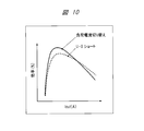
- FIG. 38 is a characteristic diagram showing a loss in the semiconductor integrated circuit device 4002.
- FIG. 38 shows three measurement results.
- a characteristic graph showing the relationship between the output current (load current) Iout (A) flowing through the output terminal T1 (FIG. 40) and the efficiency (%) of the semiconductor integrated circuit device 4002 is shown. Yes.
- the horizontal axis represents the output current
- the vertical axis represents the ratio (output power / input power) between the input power and the output power of the semiconductor integrated circuit device 4002.
- the load current (output current) Iout increases. This is because the current required by the load increases as the load becomes heavier.
- the efficiency increases when the load current Iout is relatively low, and decreases as the load current Iout increases.
- the load current (output current) Iout is equal to or less than the predetermined current value i2
- the load current (output current) Iout exceeds the predetermined current value i2.
- the type and ratio of loss were determined for light load and heavy load.
- the type and ratio of loss when the load current Iout is a current value i1 equal to or less than a predetermined current value i2 at light load is shown as “loss breakdown at light load”.
- the type and ratio of loss when the load current Iout exceeds the predetermined current value i2 when the load is heavy are shown as “loss breakdown under heavy load”. ing.
- each of “loss breakdown at light load” and “loss breakdown at heavy load” is represented by a stacked bar.
- the item of accumulation represents the type of loss.
- switching loss hereinafter also referred to as SW loss
- conduction loss hereinafter also referred to as conduction loss
- others are types of loss.
- the loss represented by others represents a loss in a logic circuit in the semiconductor integrated circuit device 4002, for example, the driver 4003.
- SW loss and conduction loss are losses in the high-side MOSFET 4005 and the low-side MOSFET 4006, and will be described with reference to FIGS. 39A and 39B.
- FIG. 39A and FIG. 39B are explanatory diagrams for explaining the SW loss and the conduction loss.
- FIG. 39A schematically shows a change in the source-drain voltage VDS, a change in the drain current IDS, and a loss P when the low-side MOSFET 4006 (high-side MOSFET 4005) transitions from off to on. ing.
- the relationship between the voltage of the second gate control signal UL supplied to the second gate electrode G2 and the first gate-drain capacitance Crss is shown as a characteristic graph.
- the horizontal axis indicates the voltage of the second gate control signal UL (in the figure, indicated as UL voltage), and the vertical axis indicates the capacitance value of the first gate-drain capacitance Crss.
- SW loss ie, switching loss P
- switching loss P is a loss that occurs when a low-side MOSFET (high-side MOSFET) transitions from off to on (or from on to off).
- VDS voltage
- IDS current
- the first gate-drain capacitance Crss is the voltage value of the second gate control signal UL supplied to the second gate electrode G2, as shown in the characteristic graph shown in the lower side of FIG. Can be reduced by reducing the negative electrode property.
- the change in the source-drain voltage VDS and the drain current IDS can be accelerated, the transition time can be shortened, and the switching loss P can be reduced. It becomes possible.
- the conduction loss is a loss proportional to the product of the on-resistance (Ron) of the low-side MOSFET (high-side MOSFET) and the square of the drain current IDS (IDS 2 ). It is.
- a characteristic graph showing the relationship between the voltage (UL voltage) of the second gate control signal UL and the on-resistance is shown on the lower side of FIG. 39B.
- the horizontal axis indicates the voltage of the second gate control signal UL
- the vertical axis indicates the on-resistance value of the low-side MOSFET (high-side MOSFET).
- the voltage (UL voltage) of the second gate control signal supplied to the second gate electrode G2 is changed from the negative voltage to the positive voltage.
- the on-resistance Ron of the low-side MOSFET (high-side MOSFET) decreases.
- the ratio of “SW loss” is higher than the losses of “conduction loss” and “other” at light load.
- the ratio of “conduction loss” is the loss of “SW loss” and “other” at heavy load.
- the ratio of “conduction loss” to the loss of the semiconductor integrated circuit device increases. That is, the ratio between the conduction loss and the switching loss in the loss of the semiconductor integrated circuit device varies depending on the load. When the load is heavy, the ratio of conduction loss is high, and when the load is light, the ratio of switching loss is high.
- both the switching loss and the conduction loss described above can be reduced.
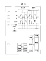
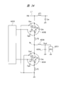
- FIG. 2A is a block diagram showing a main configuration of the driver 4003 in the semiconductor integrated circuit device 4002 according to the second embodiment.
- a second gate electrode control circuit 1000 is shown.
- the configuration of the second gate electrode control circuit 1000 shown in FIG. 1A is changed to the configuration shown in FIG. 2A in the second embodiment.
- 2A shows the control terminal T14 of the driver 4003 and the second gate electrode control circuit 1000, and the low-side MOSFET 4006 and the drive circuit 4012 shown in FIG. 1A are omitted.
- the second gate electrode control circuit 1000 shown in FIG. 2A is provided in the driver 4003 shown in FIG.
- the second gate electrode control circuit 1000 includes a positive voltage regulator 2000, a negative voltage regulator 2001, a level shifter 2003, a selection circuit 2002, and a second gate electrode drive control circuit 2004.
- Positive voltage regulator 2000 generates a positive voltage Vpos with respect to ground voltage PGND
- negative voltage regulator 2001 generates a negative voltage Vneg with respect to ground voltage PGND.
- the generated positive voltage Vpos and negative voltage Vneg are supplied to the level shifter 2003 and the selection circuit 2002.
- the second gate electrode drive control circuit 2004 receives the drive signal GL output from the drive circuit 4012 (FIG. 40), forms a control signal synchronized with the drive signal GL, and supplies it to the level shifter 2003.
- the level shifter 2003 receives the control signal formed by the second gate electrode drive control circuit 2004, shifts the high level and low level of the received control signal to voltages adapted to the positive voltage Vpos and the negative voltage Vneg, A control signal whose voltage is shifted is supplied to the selection circuit 2002.
- the selection circuit 2002 selects either the positive voltage Vpos or the negative voltage Vneg according to the voltage (high level / low level) of the supplied control signal, and selects the selected voltage (positive voltage Vpos or negative voltage Vneg). Is output to the terminal T14 as the second gate control signal UL. As shown in FIG. 1A, the terminal T14 is connected to the second gate electrode G2 of the low-side MOSFET 4006. Here, the control signal supplied from the level shifter 2003 to the selection circuit 2002 is synchronized with the drive signal GL output from the drive circuit 4012.
- the voltage of the second gate control signal UL supplied to the second gate electrode G2 of the low-side MOSFET 4006 becomes a negative voltage Vneg or a positive voltage Vpos in synchronization with the drive signal GL for turning on / off the low-side MOSFET 4006. .
- FIG. 2B shows a circuit configuration example of the selection circuit 2002, the level shifter 2003, and the second gate electrode drive control circuit 2004 described above.
- the second gate electrode drive control circuit 2004 has three inverters connected in parallel between the power supply voltage VCIN and the ground voltage CGND.
- the inverter includes a P-channel MOSFET 2009 (2008, 2007) and an N-channel type. This is a CMOS type inverter composed of MOSFETs 2015 (2014, 2013).
- the input of the inverter is connected to the output of the inverter at the previous stage and cascaded, and the drive signal GL from the drive circuit 4012 (FIG.
- the second gate electrode drive control circuit 2004 shown in FIG. 2B supplies a signal obtained by inverting the phase of the drive signal GL to the level shifter 2003 as a control signal.
- the level shifter 2003 includes an N-channel MOSFET 2012 that receives a control signal from the second gate electrode drive control circuit 2004, and a load element 2016.
- the drain of the N-channel MOSFET 2012 has a positive voltage via the load element 2016. Connected to Vpos.
- the source of the N-channel MOSFET 2012 is connected to the ground voltage CGND.
- a control signal that changes between the positive voltage Vpos and the ground voltage CGND is output from the connection node between the load element 2016 and the N-channel MOSFET 2012. That is, the control signal with the voltage shifted is output from the level shifter 2003.
- the source of the N-channel MOSFET 2012 is connected to the ground voltage CGND, but it may be connected to the negative voltage Vneg.
- the selection circuit 2002 includes two inverters connected in parallel between a positive voltage Vpos and a negative voltage Vneg, and the inverter includes an N-channel MOSFET 2011 (2010) and a P-channel MOSFET 2006 (2005). It is a CMOS inverter configured. The input of the inverter is connected to the output of the previous inverter and cascaded. The control signal from the level shifter 2003 is supplied to the input of the first stage inverter (2011, 2006), and the output of the last stage inverter (2010, 2005) is connected to the control terminal T14. Each inverter in the selection circuit 2002 operates using the positive voltage Vpos and the negative voltage Vneg as power supply voltages. Therefore, the inverter at the final stage selects the positive voltage Vpos or the negative voltage Vneg according to the control signal from the level shifter 2003, and outputs it to the control terminal T14.
- the positive voltage regulator 2000 and the negative voltage regulator 2001 can take various configurations.
- the circuits shown in FIGS. 1C and 1D can be used.
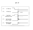
- FIGS. 3A to 3D are operation waveform diagrams of the semiconductor integrated circuit device 4002 having the second gate electrode control circuit 1000 shown in FIGS. 2A and 2B. Next, the operation of the semiconductor integrated circuit device 4002 according to Embodiment 2 will be described with reference to FIGS. 1A, 2A, 3A to 3D, and FIG.
- the horizontal axis indicates time
- the vertical axis indicates voltage
- a period (a) indicates a period in which the high-side MOSFET 4005 is on and a low-side MOSFET 4006 is off
- a period (b) indicates a period in which the high-side MOSFET 4005 is off and the low-side MOSFET 4006 is on. Yes.
- the high-side MOSFET 4005 and the low-side MOSFET 4006 are turned on / off complementarily by the drive signals GH and GL.
- FIG. 3A shows the waveform of the output voltage VSWH at the output terminal T1 of the semiconductor integrated circuit device 4002, and FIG. 3B shows the waveform of the drive signal GH from the drive circuit 4011 (FIG. 40).
- FIG. 3C shows the waveform of the drive signal GL from the drive circuit 4012 (FIG. 40).
- FIG. 3D shows the waveform of the second gate control signal UL output from the second gate electrode control circuit 1000 shown in FIG.
- the voltage of the second gate control signal UL transitions between the positive voltage Vpos and the negative voltage Vneg in synchronization with the drive signal GL.
- the source S of the low-side MOSFET 4006 is connected to a voltage terminal T2 (FIG. 1A, FIG. 40) for ground voltage. Therefore, as shown in FIG. 3D, the voltage of the second gate control signal UL is a positive voltage (positive voltage) based on the voltage at the source S of the low-side MOSFET 4006 (source voltage (GND)). Voltage Vpos) or negative voltage (negative voltage Vneg).
- Vpos positive voltage
- Vneg negative voltage
- the second gate electrode control circuit 1000 when the drive signal GL supplied to the first gate electrode G1 of the low-side MOSFET 4006 changes to a high level, in synchronization with this change, The second gate electrode control circuit 1000 outputs the positive voltage Vpos as the second gate control signal UL. On the other hand, when the drive signal GL changes to the low level, in synchronization with this change, the second gate electrode control circuit 1000 outputs the negative voltage Vneg as the second gate control signal UL.
- the drive signal GL which is the output of the drive circuit 4012, changes from the high level to the low level. Since the drive signal GL is supplied to the first gate electrode G1 of the low-side MOSFET 4006, the low-side MOSFET 4006 transitions from on to off.
- the voltage of the second gate control signal UL output from the second gate electrode control circuit 1000 changes to the negative voltage Vneg at time t1. Since the second gate electrode control signal UL is supplied to the second gate electrode G2 of the low-side MOSFET 4006, the first gate / drain of the low-side MOSFET 4006 changes when the second gate electrode control signal UL changes to the negative voltage Vneg.
- the interspace capacitance Crss is reduced. As a result, the low-side MOSFET 4006 transitions from on to off quickly, and the transition time is shortened.
- the drive signal GH that is the output signal of the drive circuit 4011 changes from the low level to the high level at time t2 after a predetermined time (dead time period) has elapsed. Change. Since the drive signal GH is supplied to the first gate electrode G1 of the high-side MOSFET 4005, the high-side MOSFET 4005 changes from off to on. As a result, the voltage of the output voltage VSWH at the output terminal T1 rises.
- both the high-side MOSFET 4005 and the low-side MOSFET 4006 are off, but the voltage VSWH at the output terminal T14 decreases. This is due to the switching loss that occurs during the period in which the low-side MOSFET 4006 transitions from on to off. In the second embodiment, since the transition period can be shortened, the switching loss can be reduced.
- the drive signal GH changes from the high level to the low level.
- the high-side MOSFET 4005 transitions from on to off.
- the drive signal GL changes from the low level to the high level. Due to the change in the drive signal GL, the low-side MOSFET 4006 transitions from off to on. Further, due to the change of the drive signal, the second gate electrode control circuit 1000 changes the voltage of the second gate electrode control signal UL that is the output signal to the positive voltage Vpos.
- the output voltage VSWH at the output terminal T14 decreases.
- the second gate electrode control signal UL having the positive voltage Vpos is supplied to the second gate electrode G2 of the low-side MOSFET 4006.
- the drive signal GL changes from the high level to the low level again. Thereafter, the operations at the times t1 to t4 described above are repeated.
- the second gate electrode control circuit 1000 that operates according to the drive signal GL moves to the second gate electrode G2.
- a positive voltage Vpos is supplied.
- a negative voltage Vneg is applied from the second gate electrode control circuit 1000 that operates according to the drive signal GL to the second gate electrode G2. Supplied.
- FIGS. 4A to 4D are explanatory diagrams for explaining the reduction of conduction loss.
- FIG. 4D shows a circuit of the low-side MOSFET 4006 described above.
- the low-side MOSFET 4006 has a source S connected to the ground voltage PGND (GND) and a drain D connected to the control terminal T14.
- Ron indicates the on-resistance when the MOSFET 4006 is turned on
- ISD indicates the source / drain current flowing through the MOSFET 4006 that is turned on. Since the low-side MOSFET 4006 can be considered to supply a current from the ground voltage to one end of the coil element 4008 (FIG. 40) when it is turned on, it is shown here as a source / drain current ISD instead of the drain current IDS.
- FIG. 4 (A) shows the waveform of the output voltage VSWH at the output terminal T1, as in FIG. 3 (A).
- FIG. 4B shows an enlarged waveform of the output voltage VSWH while the low-side MOSFET 4006 is on in FIG.
- FIG. 4C shows the waveform of the source / drain current ISD during the period when the low-side MOSFET 4011 is on.
- the broken line is a waveform of the output voltage VSWH when a negative voltage is applied to the second gate electrode G2 of the low-side MOSFET 4006, and the solid line is positive to the second gate electrode G2 of the low-side MOSFET 4006.
- the waveform of the output voltage VSWH when the voltage is applied is shown.
- the on-resistance increases.
- the on-resistance is reduced.
- the voltage due to the on-resistance is obtained by the product of resistance (Ron) and current (source / drain current ISD). Therefore, it is possible to reduce conduction loss by reducing the on-resistance. Further, it is possible to prevent the output voltage VSWH from being excessively lowered when the low-side MOSFET is turned on.
- FIG. 5 is a block diagram showing a configuration of the second gate electrode control circuit 1000 in the semiconductor integrated circuit device 4002 according to the third embodiment.
- the knowledge based on the examination of the present inventor described in the second embodiment is applied to the third embodiment. That is, the ratio of “conduction loss” and “switching loss” in the semiconductor integrated circuit device varies depending on the load, and the ratio of “conduction loss” increases as the load increases. Based on this knowledge, the loss of a high ratio is reduced and the loss of the semiconductor integrated circuit device is efficiently reduced.
- the driver 4003 (FIG. 40) is provided with the second gate electrode control circuit 1000 and the control terminal T14.
- the control terminal T14 is connected to the second gate electrode G2 of the low-side MOSFET 4006 (FIGS. 1 and 40) as in the second embodiment.
- the remaining configuration and operation are the same as those described with reference to FIG.
- the second gate electrode control circuit 1000 includes a load current detection circuit 5000, a second gate electrode drive control circuit 5001, a positive voltage regulator 5002, a negative voltage regulator 5003, and switches 5004 and 5005. As in the second embodiment, the second gate electrode control circuit 1000 forms a second gate electrode control signal UL having a positive voltage or a negative voltage with reference to the ground voltage GND, and a control terminal T14. To the second gate electrode G2 of the low-side MOSFET 4006.
- the positive voltage regulator 5002 receives the control signal 5006 output from the second gate electrode drive control circuit 5001 as an ON / OFF signal for operating / inactivating the positive voltage regulator 5002.
- the control signal 5006 instructs to operate the positive voltage regulator 5002
- the positive voltage regulator 5002 forms a positive voltage Vpos with respect to the ground voltage.
- the control signal 5006 instructs to deactivate the positive voltage regulator 5002
- the positive voltage regulator 5002 is deactivated.
- the negative voltage regulator 5003 receives the control signal 5007 output from the second gate electrode drive control circuit 5001 as an ON / OFF signal for operating / inactivating the negative voltage regulator 5003.
- the control signal 5007 instructs to operate the negative voltage regulator 5003
- the negative voltage regulator 5003 forms a negative voltage Vneg with respect to the ground voltage.
- the control signal 5007 instructs to deactivate the negative voltage regulator 5003
- the negative voltage regulator 5002 is deactivated.
- the switch 5004 is turned on / off according to the control signal 5006.
- the switch 5004 When the switch 5004 is turned on, the positive voltage Vpos formed by the positive voltage regulator 5002 is supplied to the control terminal T14.
- the on / off state of the switch 5004 is synchronized with the operation / non-operation of the positive voltage regulator 5002. That is, when the positive voltage regulator 5002 is operated by the control signal 5006, the switch 5004 is turned on, and when the positive voltage regulator 5002 is not operated by the control signal 5006, the switch 5004 is turned off.
- the switch 5005 is turned on / off according to the control signal 5007 in the same manner as the switch 5004.
- the switch 5005 When the switch 5005 is turned on, the negative voltage Vneg formed by the negative voltage regulator 5003 is supplied to the control terminal T14.
- the on / off state of the switch 5005 is synchronized with the operation / non-operation of the negative voltage regulator 5003. That is, when the positive voltage regulator 5003 is operated by the control signal 5007, the switch 5005 is turned on, and when the negative voltage regulator 5003 is not operated by the control signal 5007, the switch 5005 is turned off.
- the second gate electrode drive control circuit 5001 receives the detection signal from the load current detection circuit 5000, forms a control signal 5006 and a control signal 5007 according to, for example, a voltage of the detection signal, and operates the positive voltage regulator 5002 or the negative voltage regulator 5003.
- a switch switch 5004 or switch 5005 corresponding to the regulator to be operated (positive voltage regulator 5002 or negative voltage regulator 5003) is turned on.
- the second gate electrode control circuit 1000 receives the second gate electrode control signal UL having one of the positive voltage Vpos and the negative voltage Vneg according to the detection signal from the load current detection circuit 5000. Output to T14.
- FIG. 6A and 6B are waveform diagrams showing the operation of the second gate electrode control circuit 1000 shown in FIG. 6 (A) and 6 (B), the horizontal axis indicates time.
- FIG. 6A shows a waveform of the load current Iout flowing through the output terminal T1 of the semiconductor integrated circuit device 4002, and the vertical axis of the figure represents the current value.
- FIG. 6B shows the voltage waveform of the second gate electrode control signal UL output from the second gate electrode control circuit 1000 shown in FIG. 5, and the vertical axis in the figure represents the voltage value. ing.
- the value of the load current Iout varies depending on whether the load 4001 connected to the output terminal T13 of the power supply system 4000 (FIG. 40) is a heavy load or a light load. That is, as the load becomes heavier, the current value of the load current Iout increases.
- the load current detection circuit 5000 shown in FIG. 5 receives the load current Iout flowing through the output terminal T1 although not particularly limited, and the current value of the load current Iout exceeds a predetermined current value (current i2 in the example of FIG. 38).
- a detection signal indicating whether or not the signal is generated is supplied to the second gate electrode drive control circuit 5001.
- the second gate electrode drive control circuit 5001 operates the positive voltage regulator 5002 to turn on the switch 5004 when the detection signal indicates that the predetermined current value has been exceeded.
- the negative voltage regulator 5003 is deactivated and the switch 5005 is turned off.
- the second gate control signal UL having the positive voltage Vpos is supplied to the second gate electrode G2 of the low-side MOSFET 4005.
- the second gate electrode drive control circuit 5001 deactivates the positive voltage regulator 5002 and turns off the switch 5004. At this time, the negative voltage regulator 5003 is operated and the switch 5005 is turned on.
- the second gate control signal UL having the negative voltage Vneg is supplied to the second gate electrode of the low-side MOSFET 4005.
- switches 5004 and 5005 output the positive voltage Vpos or the negative voltage Vneg as the second gate control signal UL according to the detection signal from the load current detection circuit 5000, they can be regarded as selection circuits.
- Embodiment 3 will be described using FIGS. 6A and 6B as an example.
- load current Iout is not more than a predetermined current value (for example, i2 in FIG. 38). . Therefore, the voltage of the second gate electrode control signal UL output from the second gate electrode control circuit 1000 is a negative voltage Vneg.
- the load current Iout exceeds a predetermined value. Therefore, the voltage of the second gate electrode control signal UL output from the second gate electrode control circuit 1000 becomes a positive voltage Vpos.
- the load current Iout When the load current Iout is low, the load is light, and when the load current Iout is high, the load is heavy.
- the negative voltage Vneg is supplied to the second gate electrode G2 of the low-side MOSFET, and the switching loss is reduced.
- the load when the load is heavy (period (b)), the positive voltage Vpos is supplied to the second gate electrode G2 of the low-side MOSFET. Therefore, when the load is heavy, the conduction loss of the low-side MOSFET is reduced.
- the ratio of conduction loss is high when the load is heavy, and the ratio of switching loss is high when the load is light.
- the third embodiment when the load is heavy, the conduction loss with a high ratio can be reduced. When the load is light, the switching loss with a high ratio can be reduced. Therefore, it is possible to appropriately reduce the loss depending on the load condition.
- FIG. 7 is a block diagram showing a configuration of a semiconductor integrated circuit device 4002 according to the fourth embodiment. Also in the fourth embodiment, the knowledge based on the study of the present inventor described in the second embodiment is applied.
- the driver 4003 described with reference to FIG. 40 includes the control terminal T14, the load current detection comparator 7000, the four-cycle detection circuit 7001, the analog switch 7003, the inverter 7002, the positive voltage regulator 2000, and the negative voltage regulator 2001. Is added.
- the positive voltage regulator 2000 and the negative voltage regulator 2001 have been described with reference to FIG.
- the driver 4003 has a plurality of terminals.
- FIG. 7 shows the terminals (voltage terminal T8, output terminal T9, voltage terminal T10) described in FIG. 40 among the plurality of terminals.
- the driver 4003 has a control terminal T14 as described in the above-described embodiments.
- the first gate electrode G1 of the low-side MOSFET 4006 is connected to the output terminal T9, and the drive signal GL from the drive circuit 4012 is supplied to the first gate electrode G1 via the output terminal T9.
- the voltage terminal T10 is connected to the source S of the low-side MOSFET 4006 and further connected to the ground voltage PGND.
- the voltage terminal T8 is connected to the drain D of the low side MOSFET 4006.
- the voltage terminal T8 and the voltage terminal T10 are connected to the load current detection comparator 7000.
- the voltage terminal T8 is also connected to the output terminal T1 of the semiconductor integrated circuit device 4002, as shown in FIG. Therefore, the voltage VSWH of the voltage terminal T8 changes depending on the output of the semiconductor integrated circuit device 4002.
- the load current detection comparator 7000 includes a comparator 7004 having an inverting input terminal ( ⁇ ) and a non-inverting input terminal (+), and an offset circuit 7005.
- the non-inverting input terminal (+) of the comparator 7004 is connected to the voltage terminal T10, and the inverting input terminal ( ⁇ ) is connected to the voltage terminal T8 via the offset circuit 7005. Since various configurations of the offset circuit 7005 are conceivable, it is indicated by a battery symbol in FIG.
- the load current detection comparator 7000 compares the voltage PGND at the voltage terminal T10 with the voltage VSWH at the voltage terminal T8 when the low-side MOSFET 4006 is in the on state.
- the comparator 7004 determines whether or not the voltage VSWH + offset is higher than the ground voltage PGND. An output signal having the determination result as a high level / low level voltage is formed and output as an output signal of the load current detection comparator 7000.
- the output signal of the load current detection comparator 7000 is supplied to the 4-cycle detection circuit 7001.
- the 4-cycle detection circuit 7001 has a counter 7007 and an RS flip-flop 7006.
- the counter 7007 counts the output signal from the load current detection comparator 7000 at a predetermined cycle. For example, when the voltage VSWH + offset is higher than the ground voltage PGND, the load current detection comparator 7000 forms a high-level output signal, and when the voltage VSWH + offset is lower than the ground voltage PGND, it forms a low-level output signal.
- the counter 7000 outputs a 4times signal (indicated as 4times in the figure) when the output signal of the load current detection comparator 7000 is continuously at a high level for 4 cycles or more.
- a Reset signal (described as Reset in the figure) is output.
- the RS flip-flop 7006 of the 4-cycle detection circuit 7001 receives the 4times signal at its set terminal and the Reset signal at its reset terminal. Therefore, the RS flip-flop 7006 outputs a set output signal (for example, high level) from the output terminal Q when the 4time signal is supplied, and resets from the output terminal Q when the Reset signal is supplied. A status output signal (low level) is output. The output signal of the RS flip-flop 7006 becomes the output of the 4-cycle detection circuit 7001.
- the output signal of the 4-cycle detection circuit 7001 is used as a selection signal for the analog switch 7003.
- the analog switch 7003 has an N-channel MOSFET 7008 and a P-channel MOSFET 7009 whose source / drain paths are connected in parallel to each other, and an N-channel MOSFET 7010 and a P-channel MOSFET 7011 whose source / drain paths are connected in parallel to each other. is doing.
- the source / drain paths of the N-channel MOSFET 7008 and the P-channel MOSFET 7009 are connected between the positive voltage regulator 2000 and the control terminal T14.
- the source / drain paths of the N-channel MOSFET 7010 and the P-channel MOSFET 7011 are connected between the negative voltage regulator 2001 and the control terminal T14.
- the output signal of the four-cycle detection circuit 7001 is supplied to the gate electrode of the P-channel MOSFET 7011 and the gate electrode of the N-channel MOSFET 7008.
- the output signal of the four-cycle detection circuit 7001 is inverted in phase by an inverter 7002 and supplied to the gate electrode of the P-channel MOSFET 7009 and the gate electrode of the N-channel MOSFET 7010.
- the first analog switch constituted by the N-channel type MOSFET 7008 and the P-channel type MOSFET 7009
- the switch is turned on / off in a complementary manner.
- the first analog switch is turned on, the positive voltage Vpos is supplied to the control terminal T14 via the first analog switch.
- the second analog switch is turned on, the negative voltage Vneg is supplied to the control terminal T14 via the analog switch.
- the load current detection comparator 7000 detects whether or not the current value of the load current ISD exceeds a predetermined value. Based on the detection signal from the load current detection comparator 7000, the four-cycle detection circuit 7001 determines whether or not the load current ISD exceeds a predetermined value for four or more consecutive cycles. According to the determination result, the positive voltage Vpos or the negative voltage Vneg is supplied to the second gate electrode G2 of the low-side MOSFET 4006. As a result, the conduction loss is reduced when the load is heavy, and the switching loss is reduced when the load is light.
- 8A to 8D are waveform diagrams showing the operation of the semiconductor integrated circuit device 4002 shown in FIG.
- the horizontal axis is time.
- 8A, 8C, and 8D the vertical axis represents a voltage value, and the vertical axis in FIG. 8B represents a current value.
- FIG. 8A shows the waveform of the drive signal GL supplied to the first gate electrode G1 of the low-side MOSFET 4006, and FIG. 8B shows the current of the source / drain current ISD (load current) of the low-side MOSFET 4006.
- the waveform is shown. As described above, the source / drain current ISD becomes higher as the load becomes heavier.
- FIG. 8C shows voltage waveforms supplied to the inverting input terminal ( ⁇ ) and the non-inverting input terminal (+) of the comparator 7004.
- FIG. 8D shows the output of the 4-cycle detection circuit 7001. A signal (an output signal Q of the RS flip-flop 7006) is shown.
- the drive signal GL output from the drive circuit 4012 periodically becomes a high level, and the low-side MOSFET 4006 is periodically turned on.
- the source / drain current ISD is supplied to the coil element 4008 as a load current via the low side MOSFET.
- the voltage VSWH at the voltage terminal T8 connected to the output terminal T1 decreases.
- a voltage VSWH + offset (described as VSWH (+ offset) in the figure) formed by adding the offset voltage offset to the voltage VSWH is also lowered by the flow of the source / drain current ISD.
- the load is light and the current value of the load current (source / drain current ISD) is small. Therefore, the voltage VSWH has a voltage value higher than the ground voltage PGND, and a low level detection signal is supplied from the comparator 7004 to the four-cycle detection circuit 7001.
- the counter 7007 does not form a 4time signal because the output signal of the comparator 7004 is at a low level and is not at a high level for four or more consecutive cycles. As a result, the output signal Q of the RS flip-flop 7006 becomes a low level. Due to the low level output signal Q, the second analog switches (MOSFETs 10 and 11) are turned on, and the first analog switches (MOSFETs 8 and 9) are turned off.
- the second gate electrode control signal UL having the negative voltage Vneg is supplied to the second gate electrode G2 of the low-side MOSFET 4006. That is, when the load is light, the second gate electrode control signal UL having the negative voltage Vneg is supplied to the second gate electrode G2 of the low-side MOSFET 4006, and switching loss in the low-side MOSFET 4006 is reduced.
- the current value of the source / drain current ISD flowing through the low-side MOSFET 4006 increases.
- the voltage VSWH at the voltage terminal T8 when the low-side MOSFET 4006 is turned on is lower than the voltage value at the time before the time t1.
- the voltage VSWH + offset at the inverting input terminal ( ⁇ ) of the comparator 7004 is lower than the ground voltage PGND, and the comparator 7004 forms a high level detection signal.
- FIGS. 8B and 8C when the current value of the source / drain current ISD is continuously high for four periods, the voltage VSWH + offset is continuously decreased from the ground voltage PGND for four periods.
- the comparator 7004 forms a 4times signal.
- the flip-flop 7006 is changed to the set state, and the output signal Q of the flip-flop 7006 becomes high level (time t2).
- the first analog switches MOSFETs 7008 and 7009
- the second gate electrode control signal UL having the positive voltage Vpos is supplied from the control terminal T14 to the second gate electrode G2 of the low-side MOSFET 4006.
- the positive voltage Vpos is supplied to the second gate electrode G2 of the low-side MOSFET 4006, and the conduction loss in the low-side MOSFET 4006. Can be reduced.
- the second gate electrode control signal UL having the positive voltage Vpos is supplied to the second side MOSFET 4006. It is supplied to the gate electrode G2, and conduction loss can be reduced.
- the second gate electrode control signal UL having the negative voltage Vneg is supplied to the second gate electrode G2 of the low-side MOSFET 4006, and switching loss can be reduced.
- the load current detection comparator 7000 when the load current is high continuously for four cycles or more, it is determined that the load is heavy. Therefore, when the load current changes suddenly due to noise or the like, it can be determined that the load is heavy.
- 4 periods are an example and are not limited to this number.
- the configurations of the load current detection comparator 7000, the four-cycle detection circuit 7001, and the analog switch 7003 can be variously modified.
- the second gate electrode control signal UL supplied to the second gate electrode G2 of the low-side MOSFET 4006 in synchronization with the drive signal GL supplied to the first gate electrode G1 of the low-side MOSFET 4006. Is changed between the positive voltage Vpos and the negative voltage Vneg. That is, the polarity of the voltage supplied to the second gate electrode G2 is changed in synchronization with the on / off of the low-side MOSFET 4006.
- the polarity of the voltage of the second gate electrode control signal UL supplied to the second gate electrode of the low-side MOSFET 4006 is changed according to the load current.
- FIGS. 9A to 9F are explanatory diagrams for explaining the relationship between the change in the second gate electrode control signal UL and the light load and the heavy load in the third and fourth embodiments.
- FIG. 9A shows a waveform of the output current Iout at the output terminal T1 of the semiconductor integrated circuit device 4002.
- the output current Iout includes a current from the high-side MOSFET 4005 and a current from the low-side MOSFET (source / drain current ISD).
- FIG. 9B shows the waveform of the drive signal GH output from the drive circuit 4013 and supplied to the first gate electrode G1 of the high-side MOSFET 4005.
- FIG. 9C is output from the drive circuit 4012. The waveform of the drive signal GL supplied to the first gate electrode G1 of the low-side MOSFET 4006 is shown, and FIG.
- FIG. 9D shows the waveform of the output voltage (voltage) VSWH at the output terminal T1 (T8).
- FIG. 9E shows the waveform of the voltage at the source S of the low-side MOSFET 4006 and the second gate electrode control signal UL supplied to the second gate electrode G2 of the low-side MOSFET 4006. Since the source S of the low-side MOSFET 4006 is connected to the ground voltage PGND, the voltage becomes the ground voltage (GND).
- Fig. 9 (F) shows a loss at light load and a loss at heavy load in a stacked bar graph.
- the load is light and the current value of the output current Iout is low at a time before the time t1 (left side in the figure) with respect to the time t1. Therefore, in FIG. 9, it is indicated as “light load”.
- the load is heavy and the current value of the output current Iout is high. This state is shown as “heavy load” in FIG.
- the high-side MOSFET 4005 and the low-side MOSFET are alternately turned on / off by the drive signals GH and GL, whereby the output voltage (voltage) at the output terminal T1 (terminal T8).
- the voltage value of VSWH also changes.
- the polarity of the voltage of the second gate electrode control signal UL is not changed in synchronization with the on / off of the low-side MOSFET 4006 but the current of the load current (source / drain current ISD).
- the polarity of the voltage of the second gate electrode control signal UL changes according to the value.
- the polarity of the voltage of the second gate electrode control signal UL (with reference to the voltage at the source S of the low-side MOSFET 4006) is negative when the load is light and positive when the load is heavy.
- the second gate electrode G2 has a steady load while the low-side MOSFET 4006 is repeatedly turned on / off a plurality of times. Thus, a negative voltage is supplied.
- a positive voltage is constantly supplied to the second gate electrode G2.
- the ratio of switching loss is higher than the ratio of conduction loss at light load. Therefore, as shown on the left side of time t1 in FIG. 9F, when the load is light, a negative voltage is supplied to the second gate electrode G2, thereby reducing the switching loss and reducing the light load. Loss during loading can be reduced as a whole. 9F, the left side of the arrow indicates the breakdown of loss when the second gate electrode G2 is connected to the source S of the low-side MOSFET 4006. In the light load of FIG. 9F (before time t1), The right side shows the breakdown of loss when a negative voltage is supplied to the second gate electrode G2, as described in the third and fourth embodiments.
- FIG. 10 is a characteristic diagram showing the relationship between the output current Iout and the efficiency of the semiconductor integrated circuit device 4002.
- the horizontal axis represents the current value of the output current Iout
- the vertical axis represents the efficiency.
- the broken line indicates the case where the second gate electrode G2 is connected to the source S of the low-side MOSFET (US short), and the solid line indicates the load current as described in the third and fourth embodiments. Based on this, the voltage supplied to the second gate electrode G2 is switched between positive polarity and negative polarity. By switching based on the load current as in the third and fourth embodiments, the efficiency is improved in a part of the light load and the heavy load, and the loss is reduced as a whole.
- the pulse width (high level period) of the drive signal GL (GH) is drawn with the same width in the light load and the heavy load in order to facilitate the drawing.
- the pulse width of the drive signal GL (GH) changes as the load increases or decreases.
- the ringing of the output voltage VSWH becomes larger when the load is heavy than when the load is light.
- FIGS. 11A to 11F are diagrams for explaining the loss of light load and heavy load when a negative voltage is supplied to the second gate electrode G2 of the low-side MOSFET 4006 in the first embodiment.
- FIG. FIGS. 12A to 12F illustrate light load and heavy load loss when positive voltage is supplied to the second gate electrode G2 of the low-side MOSFET 4006 in the first embodiment. It is explanatory drawing of.
- FIGS. 11A to 11F correspond to FIGS. 9A to 9F, respectively.
- 12A to 12F also correspond to FIGS. 9A to 9F, respectively. For this reason, the differences will be mainly described here.
- the second gate electrode control signal UL is constantly set to a negative voltage or a positive voltage regardless of whether the load is light or heavy. It has become.
- FIG. 13 is a characteristic diagram showing the output current Iout and its efficiency of the semiconductor integrated circuit device 4002 according to the first embodiment. Since this figure is similar to FIG. 10, differences from FIG. 10 will be mainly described.
- a broken line indicates a case where the second gate electrode G2 of the low-side MOSFET 4006 is connected to the source S of the MOSFET 4006.
- a solid line indicates a case where a negative voltage is supplied to the second gate electrode G2
- a dashed line indicates a case where a positive voltage is supplied to the second gate electrode G2.
- the efficiency at light load is improved.
- by supplying a positive voltage to the second gate electrode G2 it is possible to improve the efficiency under heavy load.
- connection of the second gate electrode G2 to the source S of the MOSFET is based on the teaching in Patent Document 2.
- 14A to 14F show the case where a positive or negative voltage is supplied to the second gate electrode G2 of the low-side MOSFET 4006 in synchronization with the driving of the MOSFET in the second embodiment. It is explanatory drawing for demonstrating the loss of a light load and heavy load. 14A to 14F correspond to FIGS. 9A to 9F, respectively, and differences will be mainly described.
- the second gate electrode control signal UL supplied to the second gate electrode G2 of the low-side MOSFET 4006 is synchronized with the drive signal GL supplied to the first gate electrode G1 of the MOSFET. Change. That is, as shown in FIG. 14E, the second gate electrode control signal UL has a positive voltage when the low-side MOSFET 4006 is turned on by the drive signal GL, and has a negative polarity when the low-side MOSFET 4006 is turned off. Voltage. Thereby, when the low-side MOSFET 4006 is turned on, the on-resistance of the MOSFET can be reduced. On the other hand, when the low-side MOSFET 4006 is turned off, the small amount of Crss between the first gate and the drain can be reduced.
- the conduction loss when the low-side MOSFET 4006 is on (in the figure, described as “on-resistance reduction / conduction loss reduction”), whether it is light or heavy, is not possible. It is possible to reduce.
- the first gate-drain capacitance Crss since it is possible to reduce the first gate-drain capacitance Crss, it is possible to reduce the switching loss of the low-side MOSFET 4006 in both light load and heavy load (in FIG. Reduced and SW loss reduced ”). As a result, as shown in FIG. 14 (F), both the conduction loss and the switching loss can be reduced when the load is light and heavy, and the overall loss is reduced. It is possible.
- FIG. 15 is a characteristic diagram showing the relationship between the efficiency of the semiconductor integrated circuit device and its output current Iout. This figure is similar to FIG. The difference from FIG. 10 is that the solid line shows the characteristics when the second gate electrode G2 is driven according to the second embodiment (denoted as positive / negative drive in the figure). As can be understood from FIG. 10, compared to the case where the second gate electrode G ⁇ b> 2 is connected to the source S (broken line), according to the second embodiment, the efficiency is improved both in the light load and in the heavy load. The loss is reduced.
- the selection circuit 2002 selects the positive voltage Vpos and the negative voltage Vneg.
- the selection circuit 2002 it is possible to supply a voltage Vpos and a voltage Vneg having larger absolute values to the second gate electrode by improving the breakdown voltage of the MOSFET.
- the efficiency shown in FIG. 15 can be improved.
- FIG. 16A is a circuit diagram showing a configuration of a semiconductor integrated circuit device 4002 according to the fifth embodiment
- FIG. 16B is a waveform showing a waveform of the semiconductor integrated circuit device 4002 according to the fifth embodiment.
- FIG. FIG. 16A shows only the drive circuit 4011 that outputs the drive signal GH supplied to the first gate electrode G1 of the high-side MOSFET 4005 and the high-side MOSFET 4005 in the configuration shown in FIG. The rest of the configuration is the same as in FIG. 40 and is omitted here.
- the driver 4003 is provided with a control terminal T15.
- a driver 4003 is provided with a second gate electrode control circuit 1600 that supplies a second gate control signal UH to the second gate electrode G2 of the high-side MOSFET 4005 via the control terminal T15.
- the second gate electrode control circuit 1600 includes a variable voltage source 1601, generates a second gate control signal UH having a predetermined voltage, and supplies the second gate control signal UH to the second gate electrode G2 of the high-side MOSFET 4005 via the control terminal T15.
- the predetermined voltage is, for example, 2V
- the second gate signal UH having a voltage value of 2V is supplied from the second gate electrode control circuit 1600 to the second gate electrode G2 of the high-side MOSFET 4005 via the control terminal T15.
- the drive signal GH is supplied from the drive circuit 4011 to the first gate electrode G1 of the high-side MOSFET 4005, and the high-side MOSFET 4005 is on / off controlled in accordance with the drive signal GH.
- the output terminal T1 of the semiconductor integrated circuit device 4002, the voltage terminal T8 of the driver 4003, and the source S of the high-side MOSFET 4005 are connected to each other.
- the high-side MOSFET 4005 and the low-side MOSFET 4006 are alternately turned on / off. Therefore, the voltage value of the voltage at the output terminal T1, the voltage terminal T8, and the source S of the high side MOSFET 4005 varies with time. In other words, the value of the voltage at the source S of the high-side MOSFET 4005 changes by turning on / off the high-side MOSFET 4005 and the low-side MOSFET 4006.
- this voltage amplitude is, for example, 12V
- the voltage value of the second control signal UH is 2V as described above
- the voltage terminal T8 is almost grounded by turning on the low side MOSFET 4006 immediately before the high side MOSFET 4005 is turned on. Since it is a voltage, 2 V, which is a positive voltage with respect to the source S (voltage terminal T8), is supplied to the second gate electrode G2 of the high-side MOSFET 4005.
- the voltage at the source S (voltage terminal T8) of the MOSFET is 12 V due to the high-side MOSFET 4005 being turned on. Therefore, the second gate electrode G2 of the high-side MOSFET 4005 has Therefore, -10V, which is a negative voltage with respect to the voltage at the source S of the MOSFET, is supplied.
- FIG. 16B shows the waveform of the voltage VSWH (source voltage (VSWH)) at the source S (voltage terminal T8) of the high-side MOSFET 4005 and the waveform of the second control signal UH.
- the horizontal axis is time
- the vertical axis is voltage value.
- FIG. 16B when the high-side MOSFET 4005 is turned on is shown as a period (a), and when the high-side MOSFET 4005 is turned off is shown as a period (b). Note that there is a period in which the voltage at the source S (source voltage) VSWH is lower than the ground voltage (0 V), which indicates a change caused by the counter electromotive force generated by the coil element 4008 (FIG. 40). .
- the second gate electrode G2 of the high-side MOSFET 4005 has a negative polarity with respect to the source voltage (VWSH) at the source S.
- VWSH source voltage
- FIGS. 17A to 17E show the second gate electrode control circuit 1600 that supplies a second gate control signal UH having a predetermined voltage to the second gate electrode G2 of the high-side MOSFET 4005 in the fifth embodiment. It is explanatory drawing for demonstrating the loss of the light load and heavy load at the time of supplying from.
- FIGS. 17A to 17C and 17E correspond to FIGS. 9A to 9C and 9F, respectively.
- FIG. 17D is similar to FIGS. 9D and 9E, and FIG. 17D shows the voltage (source voltage) VSWH at the source S (voltage terminal T8) of the high-side MOSFET 4005. And the waveform of the second gate control signal UH. Differences from FIG. 9 will be mainly described.
- a predetermined positive voltage is formed by the second gate electrode control circuit 1600, and the second gate electrode G2 of the high-side MOSFET 4005 is formed. Is constantly supplied. Thus, when the high-side MOSFET 4005 is turned off, a negative voltage is supplied to the source of the second gate electrode G2. Since it is constantly supplied, the high-side MOSFET 4005 can reduce the switching loss when changing from on to off, both in light load and heavy load (in FIG. (Turn Off) “Capacity reduction / SW loss reduction”.
- This reduction in switching loss makes it possible to reduce the loss as a whole when the load is light, as shown in FIG. This is because, as described in FIG. 38, the ratio of the switching loss is high when the load is low.
- the first gate-drain capacitance Crss may increase.
- the voltage supplied to the second gate electrode G2 is negative with respect to the voltage at the source, as can be understood from FIG. During this period, the on-resistance may increase.
- FIG. 18 is a characteristic diagram showing the relationship between the efficiency of the semiconductor integrated circuit device 4002 according to the fifth embodiment and its output current Iout.
- FIG. 18 is similar to FIG. 10 described above. The difference is that the relationship between the output current Iout and the efficiency of the semiconductor integrated circuit device 4002 of the fifth embodiment is shown as a solid line (constant voltage). Yes.
- FIG. 18 also shows that the efficiency is improved at a light load, and the loss is reduced.
- FIG. 19A is a circuit diagram showing a configuration of a semiconductor integrated circuit device 4002 according to Embodiment 6, and FIG. 19B shows a waveform of the semiconductor integrated circuit device 4002 shown in FIG. FIG.
- the configuration shown in FIG. 19A is similar to the configuration shown in FIG. 16A described in Embodiment 5, and therefore the differences will be mainly described.
- the difference from the configuration shown in FIG. 16A is that the configuration of the second gate electrode control circuit 1600 is different. That is, in FIG. 19A, the second gate electrode control circuit 1600 has resistance elements 1900 and 1901 directly connected between the voltage terminal T8 and the ground voltage CGND. Resistive elements 1900 and 1901 divide the voltage (source voltage) VSWH at the source of high-side MOSFET 4005. The voltage obtained by the voltage division is taken out from a connection node between the resistance elements 1900 and 1901 and is supplied from the second gate electrode control circuit 1600 to the control terminal T15 as the second gate control signal UH. The control terminal T15 is connected to the second gate electrode G2 of the high side MOSFET 4006. Therefore, a voltage corresponding to the voltage VSWH at the source S of the high side MOSFET 4005 is supplied to the second gate electrode G2 of the high side MOSFET 4005 as the second gate control signal UH.
- FIG. 19B shows the waveform of the source voltage (voltage at the voltage terminal T8) VSWH at the source S of the high-side MOSFET 4005 in FIG. 19A and the waveform of the second gate control signal UH formed by voltage division. It is shown.
- a period (a) indicates a period during which the high-side MOSFET 4005 changes from off to on
- a period (b) indicates a period during which the high-side MOSFET 4005 changes from on to off.
- the second gate control signal UH is formed by dividing the voltage at the source of the high-side MOSFET 4005, the voltage value changes following the change in the voltage VSWH at the source.
- the voltage of the second gate control signal UH is a divided voltage of the source voltage VSWH, so that the voltage supplied to the second gate electrode G2 Is lower than the source voltage VSWH and has a negative polarity with respect to the source voltage VSWH.
- the first gate-drain capacitance Crss can be reduced, and the switching loss can be reduced as in the fifth embodiment. .
- the sixth embodiment it is possible to suppress an increase in the first gate electrode-drain capacitance Crss when the high-side MOSFET 4005 is turned on from off, and when the high-side MOSFET 4005 is turned off from on. It is possible to reduce the first gate-drain capacitance Crss. Therefore, it is possible to reduce the switching loss of the high side MOSFET as compared with the fifth embodiment.
- 20A to 20E are explanatory diagrams for explaining light load and heavy load loss in the semiconductor integrated circuit device 4002 shown in the sixth embodiment.
- 20A to 20E correspond to FIGS. 17A to 17E, respectively. For this reason, the differences will be mainly described here.
- the waveform shown in FIG. 20D is different from the waveform shown in FIG.
- the voltage of the second gate signal UH supplied to the second gate electrode G2 of the high side MOSFET 4005 changes following the change of the voltage VSWH at the source of the high side MOSFET 4005.
- the voltage amplitude of the second gate control signal UH is smaller than the voltage at the source of the high-side MOSFET 4005 (source voltage VSWH).
- FIG. 21 is a characteristic diagram showing the relationship between the efficiency of the semiconductor integrated circuit device 4002 according to the sixth embodiment and its output current Iout.
- FIG. 21 is similar to FIG. 18 described above. The difference is that the relationship between the output current Iout and the efficiency of the semiconductor integrated circuit device 4002 according to the fifth embodiment is shown as a one-dot broken line (constant voltage). The relationship between the output current Iout and the efficiency of the semiconductor integrated circuit device 4002 according to the sixth embodiment is shown as a solid line (VSWH divided voltage). As understood from FIG. 21, when the current value of the output current Iout is small, that is, when the load is light, the efficiency is improved and the loss is reduced.
- FIG. 22A is a circuit diagram showing a configuration of the semiconductor integrated circuit device 4002 according to Embodiment 7, and FIG. 22B shows a waveform of the semiconductor integrated circuit device 4002 shown in FIG. FIG. Since the structure shown in FIG. 22A is similar to the structure shown in FIG. 19A described in Embodiment 6, the differences will be mainly described.
- a difference from the configuration shown in FIG. 19A is that the configuration of the second gate electrode control circuit 1600 is different. That is, in FIG. 19A, the second gate electrode control circuit 1600 forms a divided voltage by the resistance element 1900 and the resistance element 1901 and uses the formed divided voltage as the second gate control signal UH.
- the second gate electrode control circuit 1600 according to the seventh embodiment is connected between the resistance element 2200 connected between the voltage terminal T8 and the control terminal T15, and between the control terminal T18 and the ground voltage CGND.
- the load current detection circuit 2202 detects whether or not the current value of the output current Iout flowing through the output terminal T1 of the semiconductor integrated circuit device 4002 exceeds a predetermined current value, and determines whether or not it exceeds the predetermined current value.
- the detected signal is supplied to the high side voltage control circuit 2203.
- the high side voltage control circuit 2203 changes the resistance value of the variable resistance element 2201 in accordance with the supplied detection signal.
- the resistance element 2200 and the variable resistance element 2201 are connected in series between the output terminal T8 and the ground voltage CGND, and a connection node is connected to the control terminal T15.
- the voltage (source voltage) VSWH at the source S of the high-side MOSFET 4005 is divided by the resistance element 2200 and the variable resistance element 2201, and the second gate control signal UH having a divided voltage formed by voltage division. Is supplied to the second gate electrode G2 of the high-side MOSFET 4005 via the control terminal T15.
- the resistance value of the variable resistance element 2201 is changed by the high-side voltage control circuit 2203 in accordance with a detection signal from the load current detection circuit 2202. That is, the value of the voltage supplied to the second gate electrode G2 of the high side MOSFET 4005 changes according to the value of the load current.
- the high side voltage control circuit 2203 increases the resistance value of the variable resistance element 2201.
- the resistance value of the variable resistance element 2202 is set to the first resistance value when the current value of the load current Iout is equal to or lower than the predetermined current value, and the current value of the load current Iout exceeds the predetermined current value.
- the second resistance value is higher than the first resistance value.
- the predetermined current value is a load current value that divides a light load and a heavy load.
- the current value i2 is set to a predetermined current value.
- FIG. 22B shows the waveform of the source voltage (voltage at the voltage terminal T8) VSWH at the source S of the high-side MOSFET 4005 in FIG. 22A, the variable resistance element 2201, and the resistance element (fixed resistance element) 2200.
- the waveform of the second gate control signal UH formed by the partial pressure is shown. Since the waveform shown in FIG. 22B is similar to the waveform shown in FIG. 19B, the difference will be mainly described.
- a period (a) indicates a period during which the high-side MOSFET 4005 changes from off to on, and a period (b) indicates a period during which the high-side MOSFET 4005 changes from on to off.
- the operations in the periods (a) and (b) are the same as those in FIG. That is, the voltage value of the second gate control signal UH changes following the change of the voltage VSWH at the source.
- the high-side MOSFET 4005 changes from off to on (period (a))
- the voltage of the second gate control signal UH is a divided voltage of the source voltage VSWH, so that the voltage supplied to the second gate electrode G2 Is lower than the source voltage VSWH and becomes a negative voltage.
- the first gate-drain capacitance Crss can be reduced, and switching loss can be reduced.
- the seventh embodiment when the load current Iout exceeds a predetermined value, the resistance value of the variable resistance element 2201 is increased by the high-side voltage control circuit 2003.
- the high-side MOSFET 4005 when the high-side MOSFET 4005 is on, the voltage supplied to the second gate electrode G2 approaches the source voltage VSWH.
- an increase in on-resistance of high-side MOSFET 4005 is suppressed, and an increase in conduction loss is suppressed, and it is possible to reduce the conduction loss of high-side MOSFET as compared with the fifth and sixth embodiments.
- FIGS. 23A to 23E are explanatory diagrams for explaining light load and heavy load loss in the semiconductor integrated circuit device 4002 shown in the seventh embodiment.
- FIGS. 23A to 23E correspond to FIGS. 20A to 20E, respectively. For this reason, the differences will be mainly described here.
- the waveform under heavy load is different from the waveform shown in FIG. 20 (D).
- the high side voltage control circuit 2203 based on the detection signal from the load current detection circuit 2202, the high side voltage control circuit 2203 recognizes that the current value of the load current Iout has exceeded a predetermined value, and the resistance of the variable resistance element 2201 Increase the value.
- the high-side voltage control circuit 2203 does not increase the resistance value of the variable resistance element 2201. Therefore, when the load is light, the switching loss of the high-side MOSFET 4005 is reduced as in the sixth embodiment (see the light load in FIG. 23E).
- the voltage of the second gate control signal UH supplied to the second gate electrode G2 of the high-side MOSFET 4005 changes in the same manner as the change of the source voltage VSWH of the high-side MOSFET 4005.
- a voltage value close to the voltage value of VSWH is reached.
- the second gate electrode G2 of the high-side MOSFET 4005 is in a voltage-like state that is shorted with its source S (in FIG. 23D, “US short”). (US Short) Similar ”).
- US short US Short
- FIG. 24 is a characteristic diagram showing the relationship between the efficiency of the semiconductor integrated circuit device 4002 according to the seventh embodiment and its output current Iout.
- FIG. 24 is similar to FIG. 21 described above. The difference is that the relationship between the output current Iout and the efficiency of the semiconductor integrated circuit device 4002 according to the sixth embodiment is indicated by a one-dot broken line (VSWH divided voltage). The relationship between the output current Iout and the efficiency of the semiconductor integrated circuit device 4002 according to the seventh embodiment is shown by a solid line (voltage division + voltage division ratio control). As understood from FIG. 21, when the current value of the output current Iout is large, that is, when the load is heavy, the efficiency is improved compared to the sixth embodiment, and the loss is reduced.
- the resistance element connected between the control terminal T15 and the ground voltage CGND is a variable resistance element.
- the resistance element connected between the control terminal T15 and the ground voltage CGND is a fixed resistance element
- the resistance element connected between the output terminal T8 and the control terminal T15 is a variable resistance element
- the resistance value thereof. May be controlled by the high-side voltage control circuit 2203. In this case, control is performed so that the resistance value of the variable resistance element becomes small under heavy load.
- both the resistance elements 2200 and 2201 may be variable resistance elements, and the resistance values of the resistance elements 2200 and 2201 may be controlled by the high-side voltage control circuit 2203.
- the resistance value of the variable resistance element may be changed in three or more steps instead of the two-step change in the first resistance value and the second resistance value.
- a detection signal whose value continuously changes according to the load current is output from the load current detection circuit 2202, and the high-side voltage control circuit 2003 continuously sets the resistance value of the variable resistance element according to this detection signal. It may be changed as desired.
- FIG. 25 is a waveform diagram showing a waveform of the second gate control signal UH formed by the second gate electrode control circuit 1600 included in the semiconductor integrated circuit device 4002 according to the eighth embodiment.
- the second gate control signal UH formed by the second gate electrode control circuit 1600 in the eighth embodiment is supplied to the second gate electrode G2 of the high side MOSFET 4005 through, for example, the control terminal T15 shown in FIG.
- the horizontal axis represents time
- the vertical axis represents voltage.
- the second gate electrode control circuit 1600 uses the source of the high-side MOSFET 4005.
- a second gate control signal UH having a negative voltage V1 with respect to the source voltage (output terminal T8) VSWH at S is supplied to the second gate electrode G2 of the high-side MOSFET 4005.
- the second gate electrode control circuit 1600 changes the voltage value of the second gate control signal UH from the voltage V1 to the voltage V2 immediately before the high-side MOSFET 4005 is changed from OFF to ON by the drive signal GH.
- the voltage value V2 at this time is set to be higher than the source voltage VSWH of the high-side MOSFET 4005 when the high-side MOSFET 4005 is turned on.
- the second gate electrode control circuit 1600 changes the voltage value of the second gate control signal UH from the voltage V2 to the voltage V3. change.
- the voltage V3 is set to a voltage value having a negative polarity with respect to the voltage value of the source voltage VSWH of the high-side MOSFET at this time.
- the second gate electrode control circuit 1600 changes the voltage value of the second gate control signal UH to the voltage V2, and then changes it to the voltage value V1.
- the source voltage VSWH is applied to the second gate electrode G2 when the high-side MOSFET 4005 transitions from the off state to the on state (time t1).
- a negative voltage is supplied.
- the high side MOSFET 4005 is changed from the on state to the off state (time t2)
- a negative voltage is supplied to the second gate electrode G2 with respect to the source voltage VSWH of the high side MOSFET 4005 at that time. It will be.
- the first gate-drain capacitance Crss of the high side MOSFET 4005 can be reduced, and the switching loss is reduced. It becomes possible.
- the second gate electrode control circuit 1600 that forms the second gate control signal UH that changes the voltage as shown in FIG. 25 includes, for example, a negative voltage generation circuit that forms the voltage V1, a positive voltage generation circuit that forms the voltage V2, It can be realized by a logic circuit that receives the control signal f from the driver 4004 described in FIG. For example, based on the control signal f, the change to the high level of the drive signal GH supplied to the first gate electrode G1 of the high-side MOSFET 4005 is grasped before the change, and the voltage value of the second gate control signal UH is set to the voltage Change to V2.
- the change to the low level of the drive signal GH may be grasped before the change, and the voltage value of the second gate control signal UH may be changed from the voltage V2 to the voltage V3.
- the voltage V3 can be generated from the voltage V2, for example.
- the voltage V3 may be obtained in advance by measurement, or the voltage at the output terminal T8 may be measured.
- FIG. 26 is a characteristic diagram showing the relationship between the efficiency of the semiconductor integrated circuit device 4002 according to the eighth embodiment and its output current Iout.
- FIG. 26 is similar to FIG. 24 described above. The difference is that the relationship between the output current Iout and the efficiency of the semiconductor integrated circuit device 4002 according to the seventh embodiment is indicated by a one-dot broken line (divided voltage + divided voltage ratio). The relationship between the output current Iout and the efficiency of the semiconductor integrated circuit device 4002 according to the eighth embodiment is shown as a solid line (the eighth embodiment).
- the eighth embodiment since both the switching loss and the conduction loss are reduced, as can be understood from FIG. 26, when the current value of the output current Iout is small or large, that is, when the load is light. Even under heavy loads, the efficiency is improved and the loss is reduced.
- FIG. 27 is a block diagram showing a configuration of a semiconductor integrated circuit device 4002 according to the ninth embodiment.
- the semiconductor integrated circuit device 4002 shown in the figure is similar to the semiconductor integrated circuit device 4002 described above with reference to FIG. 40, and the same reference numerals are given to the same elements. Here, only the differences will be mainly described.
- the driver 4003 has a load current detection circuit 2700, a second gate electrode control circuit 2701, a control terminal T14, and a control terminal T15 with respect to the driver 4003 shown in FIG.
- the load current detection circuit 2700 is connected to the voltage terminal T2 of the semiconductor integrated circuit device 4002 via the voltage terminal T10 of the driver 4003 and to the output terminal T1 of the semiconductor integrated circuit device 4002 via the voltage terminal T8 of the driver 4003. Yes.
- the load current detection circuit 2700 corresponds to the load current detection circuit (including the load current detection comparator 7000 (FIG. 7)) already described in the plurality of embodiments.
- the load current detection circuit 2700 corresponds to the load current detection circuit 5000 (FIG. 5) or 2202 (FIG. 22) described in the third embodiment or the seventh embodiment.
- the load current detection circuit 2700 detects the output current Iout flowing through the output terminal T1 of the semiconductor integrated circuit device 4002 as a load current, and whether or not the output current Iout exceeds a predetermined current value (for example, the current i2 in FIG. 38). And a detection signal is supplied to the second gate electrode control circuit 2701.
- a predetermined current value for example, the current i2 in FIG. 38.
- the second gate electrode control circuit 2701 forms the second gate control signal UH and the second gate control signal UL according to the detection signal from the load current detection circuit 2700.
- the formed second gate control signal UH is used to control the second gate electrode G2 of the high-side MOSFET 4005, and the second gate control signal UL is used to control the second gate electrode G2 of the low-side MOSFET 4006. It is done. Therefore, the second gate control signal UH is supplied to the second gate electrode G2 of the high-side MOSFET 4005 via the control terminal T15, and the second gate control signal UL is supplied to the second gate electrode of the low-side MOSFET 4006 via the control terminal T14. Supplied to G2.
- the second gate electrode control circuit 2701 When the detection signal from the load current detection circuit 2700 indicates that the output current Iout flowing through the output terminal T1 exceeds the predetermined current value, the second gate electrode control circuit 2701 A second gate control signal UH having a positive voltage with respect to the voltage VSWH at the source S of the MOSFET 4005 is formed. In this case, the second gate electrode control circuit 2701 generates a second gate control signal UL having a positive voltage with respect to the voltage PGND at the source S of the low-side MOSFET 4006.
- the second gate electrode control circuit 2701 when a detection signal indicating that the output current Iout is less than or equal to a predetermined current value is supplied to the second gate electrode control circuit 2701, the second gate electrode control circuit 2701 is connected to the voltage at the source S of the high-side MOSFET 4005. A second gate control signal UH having a negative voltage with respect to VSWH is formed, and a second gate control signal UL having a negative voltage with respect to the voltage PGND at the source S of the low-side MOSFET 4006 is formed.
- the current value of the load current (output current) Iout increases.
- the current i2 is set as the current value of the load current that distinguishes the light load from the heavy load.
- the voltage supplied to the second gate electrode G2 becomes positive with respect to the voltage at the source, the on-resistance when the high-side MOSFET 4005 and the low-side MOSFET 4006 are turned on is reduced. As a result, the conduction losses of the high-side MOSFET 4005 and the low-side MOSFET 4006 at the time of heavy load are reduced.
- the second gate electrode G2 of the high-side MOSFET 4005 has a negative voltage with respect to the voltage at the source S. Therefore, a negative voltage with respect to the voltage at the source S is also steadily supplied to the second gate electrode G2 of the low-side MOSFET 4006.
- the first gate electrode-drain capacitance Crss in each of the high-side MOSFET 4005 and the low-side MOSFET 4006 is reduced, and the switching loss is reduced.
- the second gate electrode control circuit 2701 is not particularly limited, but can be constituted by a positive voltage regulator, a negative voltage regulator, and four switches.
- the positive voltage regulator generates, for example, the positive voltage Vpos described in FIG. 5 and the positive voltage V2 described in FIG.
- the negative voltage regulator generates the negative voltage Vneg described in FIG. 5 and the voltage V1 described in FIG. Of the four switches, two are paired and two pairs are made.
- a positive voltage Vpos and a negative voltage Vneg are supplied to one end of each of the pair of switches.
- a two-gate control signal UL is output.
- a positive voltage V2 and a negative voltage V1 are supplied to one end of the other pair of switches, and the second gate control signal UH is output from the other end of the other pair of switches.
- the two pairs of switches are controlled depending on whether or not the detection signal from the load current detection circuit 2700 exceeds a predetermined value, and the voltage supplied to the second gate electrode G2 of each of the high-side MOSFET 4005 and the low-side MOSFET 4006 is selected. To do.
- conduction loss and switching loss can be reduced according to the load. That is, when the load is heavy, it is possible to reduce the conduction loss having a high ratio at that time in both the high-side MOSFET 4005 and the low-side MOSFET 4006. When the load is light, the switching loss having a high ratio at that time can be reduced for both MOSFETs. Can be reduced. In other words, the loss is appropriately reduced according to the load at that time, and the loss can be reduced regardless of the load change.
- ⁇ Modification 1> In the description of FIG. 27 described above, a voltage higher than the voltage at the source S is constantly supplied to the second gate electrode G2 of the high-side MOSFET 4005 when the load is heavy.
- the configuration of the seventh embodiment may be applied to the high side MOSFET 4005 in FIG.
- the structure described in Embodiment 3 may be applied to the low-side MOSFET 4006 in FIG.
- the load current detection circuit 2700 shown in FIG. 27 includes, for example, the load current detection circuit 5000 shown in FIG. 5 and the load detection circuit 2202 shown in FIG.
- the second gate electrode control circuit 2701 shown in FIG. 27 includes the second gate electrode drive control circuit 5001, the positive voltage regulator 5002, the negative voltage regulator 5003, the switches 5004 and 5005 shown in FIG.
- the voltage of the second gate electrode G2 of the high side MOSFET 4005 changes following the voltage at the source S of the high side MOSFET. Therefore, it is possible to reduce the voltage regulator for forming the positive voltage V2 and the negative voltage V1 supplied to the second gate electrode G2 of the high side MOSFET 4005.
- FIG. 28 is a block diagram showing a configuration of a semiconductor integrated circuit device 4002 according to a modification of the ninth embodiment.
- the configuration shown in FIG. 28 is similar to the configuration shown in FIG. Here, the differences will be mainly described.
- reference numeral 2802 denotes a MOSFET that does not have the second gate electrode G2.
- Such a MOSFET 2802 is known as a trench type MOSFET, for example.
- an N ⁇ type semiconductor layer 3704 is formed with an insulating layer and a metal layer 3708 corresponding to the second gate electrode G2.
- MOSFET hereinafter referred to as 1 gate electrode MOSFET.
- 2800 is a load current detection circuit
- 2801 is a second gate electrode control circuit.
- the load current detection circuit 2800 detects an output current (load current) Iout flowing through the output terminal T1, and supplies a detection signal indicating whether or not the load current Iout exceeds a predetermined current value to the second gate electrode control circuit 2801. To do.
- the second gate electrode control circuit 2801 generates a second gate control signal UL according to the detection signal and supplies it to the second gate electrode G2 of the low-side MOSFET 4006 via the control terminal T14.
- the high-side MOSFET is composed of one gate electrode MOSFET 2802, the second gate control signal UH for the high-side MOSFET is not formed.
- the load current detection comparator 7000 in FIG. 7 is regarded as the load current detection circuit 2800 in FIG. Further, the four-period detection circuit 7001, the analog switch 7003, the inverter 7002, the positive voltage regulator 2000, and the negative voltage regulator 2001 described in FIG. 7 are regarded as the second gate electrode control circuit 2801 in FIG.
- the loss of the low-side MOSFET 4006 is reduced according to the load condition at that time, and the power consumption of the semiconductor integrated circuit device 4002 and the power supply system can be reduced.
- FIG. 29 is a block diagram showing a configuration of a semiconductor integrated circuit device 4002 according to a modification of the ninth embodiment.
- the configuration shown in FIG. 29 is similar to the configuration shown in FIG. Here, the differences will be mainly described.
- reference numeral 2902 denotes a one-gate electrode MOSFET that does not have the second gate electrode G2.
- 2900 is a load current detection circuit
- 2901 is a second gate electrode control circuit.
- the load current detection circuit 2900 has the same configuration as the load current detection circuit 2800 described in the second modification, detects the output current (load current) Iout flowing through the output terminal T1, and the load current has a predetermined current value. Is supplied to the second gate electrode control circuit 2901.
- the second gate electrode control circuit 2901 generates a second gate control signal UH according to the detection signal and supplies it to the second gate electrode G2 of the high-side MOSFET 4005 via the control terminal T15.
- the second gate control signal UL for the low-side MOSFET is not formed.
- the load current detection circuit 2900 and the second gate electrode control circuit 2901 As the load current detection circuit 2900 and the second gate electrode control circuit 2901, the configuration described in the seventh embodiment or the ninth embodiment is applied.
- the load current detection circuit 2202 shown in FIG. 22A is regarded as the load current detection circuit 2900 in FIG. Further, the high-side voltage control circuit 2203, the fixed resistance element 2200, and the variable resistance element 2201 shown in FIG. 22A are regarded as the second gate electrode control circuit 2901.
- the voltage V1 is supplied to the second gate electrode G2 of the high-side MOSFET 4005 when the load is light, and the second gate of the high-side MOSFET 4005 when the voltage V2 is a heavy load. Supplied to the electrode G2.
- the loss of the high-side MOSFET 4005 is reduced according to the load condition at that time, and the power consumption of the semiconductor integrated circuit device 4002 and the power supply system can be reduced.
- FIG. 30 is a block diagram showing a configuration of a semiconductor integrated circuit device 4002 according to the tenth embodiment.
- the configuration shown in FIG. 30 is similar to the configuration of the semiconductor integrated circuit device 4002 shown in FIG. Since the same reference numerals are given to the same components, different portions will be mainly described.
- the semiconductor integrated circuit device 4002 has a terminal T16, and the second gate electrode G2 of the low-side MOSFET 4006 is connected to the terminal T16.
- the semiconductor integrated circuit device 4002 is a package in which a plurality of semiconductor chips are sealed. Therefore, the terminal T16 corresponds to an external terminal provided in the package.
- a resistance element 3000 is connected between a terminal (external terminal) T16 provided in the package and the ground voltage PGND. In this case, the resistance element 3000 is provided outside the package.
- FIG. 31 is a circuit diagram focusing on the high-side MOSFET 4005 and the low-side MOSFET 4006 in the semiconductor integrated circuit device 4002 shown in FIG.
- FIG. 31 attention is paid to the high-side MOSFET 4005 and the low-side MOSFET 4006, and thus the configuration of the driver 4003 is omitted.
- parasitic resistance, parasitic capacitance, and parasitic inductance are also clearly shown.
- a high side MOSFET 4005 and a low side MOSFET 4006 have the same configuration.
- the low-side MOSFET 4006 (high-side MOSFET 3005) includes a parasitic capacitance Cgs formed between the first gate electrode G1 and the source S, a parasitic capacitance Ced formed between the second gate electrode G2 and the drain D, and the source S It has a parasitic capacitance Cds formed between the drain D and a parasitic diode DD formed by connecting the back gate to the source S.
- the first gate electrodes G1 of the high-side MOSFET 4005 and the low-side MOSFET 4006 are connected to the driver 4003 and driven by drive signals GH and GL from the driver 4003.
- the drain D of the high-side MOSFET 4005 is connected to the wiring L1, and the input voltage VIN is supplied from the terminal (external terminal) T6 via the wiring L1.
- a capacitive element Cin is connected to the wiring L1 for stabilization.
- the wiring L1 is accompanied by a parasitic inductance LP1.
- the drain of the high side MOSFET 4005 is connected to the switching node Ns through the parasitic inductance LP3, and the switching node Ns is connected to the drain D of the low side MOSFET 4006.
- the source S of the low side MOSFET 4006 is connected to the ground voltage PGND via a parasitic inductance LP2.
- the switching node Ns is connected to one end of the coil element 4008, and the other end of the coil element 4008 is connected to the smoothing capacitor 4009.
- a CPU is illustrated as the load 4001.
- the second gate electrode G2 of the high-side MOSFET 4005 is connected to the ground voltage PGND, although not particularly limited. Further, the second gate electrode G2 of the low-side MOSFET 4006 is connected to the ground voltage PGND via a terminal T16 (FIG. 30) and a resistance element 3000 provided outside the package.
- a snubber circuit is configured by the parasitic capacitance Ced formed between the second gate electrode G2 of the low-side MOSFET 4006 and the source S of the MOSFET 4006 and the external resistance element 3000. This snubber circuit suppresses voltage ringing at the switching node Ns.
- 32A to 32E are waveform diagrams showing the operation of the configuration shown in FIG. The operation will be described below with reference to FIGS. 31 and 32A to 32E.
- FIG. 32 shows a voltage change (Lo-Side Vgs) between the first gate electrode G1 and the source of the low-side MOSFET 4006, and FIG. 32B shows the first gate electrode G1 and the source of the high-side MOSFET 4005.
- a voltage change (Hi-Side Vgs) is shown. In other words, voltage changes of the drive signals GL and GH from the driver 4003 are shown.
- FIG. 32C shows a current (Body Diode Forwarding Current) flowing through the parasitic diode DD (body diode) of the low-side MOSFET 4006.
- FIG. 32E shows the voltage at the switching node Ns in the case where a snubber circuit is configured by providing the external resistor element 3000.
- FIG. 32D shows the voltage at the switching node Ns when the snubber circuit is not configured.
- the resistance element 3000 By connecting the external resistance element 3000 to the terminal T16, the resistance element 3000 is connected to the second gate electrode G2 of the low-side MOSFET 4006.
- the parasitic capacitance Ced and the external resistance element 3000 are connected to the ground voltage PGND. It is connected in series with the switching node Ns and operates as a snubber circuit that suppresses ringing at the switching node Ns. Thereby, as shown in FIG. 32E, ringing at the switching node Ns is suppressed as compared with FIG. That is, ringing when the high-side MOSFET 4005 is turned on is suppressed, and the output voltage Vout with suppressed noise can be formed.
- the amount of ringing to be suppressed can be adjusted by adjusting the resistance value of the external resistance element 3000. Therefore, it is more desirable that the resistance element 3000 be connected to the terminal T16 of the package that is the semiconductor integrated circuit device 4002 outside the package.
- FIG. 33 is a block diagram showing a configuration of a semiconductor integrated circuit device 4002 according to the eleventh embodiment.
- the configuration shown in FIG. 33 is similar to the configuration of the semiconductor integrated circuit device 4002 shown in FIG. 40, and therefore the differences will be mainly described.
- the second gate electrode G2 of the high side MOSFET 4005 is connected to the ground voltage PGND inside the semiconductor integrated circuit device 4002.
- FIGS. 34 and 35 a description will be given with reference to FIGS. 34 and 35. By doing so, it is possible to reduce noise when the high-side MOSFET 4005 is turned on.
- FIG. 34 is a circuit diagram focusing on the high-side MOSFET 4005 and the low-side MOSFET 4006 in the semiconductor integrated circuit device 4002 shown in FIG.
- the circuit shown in FIG. 34 is similar to the circuit shown in FIG.
- the difference between FIG. 31 and FIG. 34 is that, in FIG. 34, the second gate electrode G2 of the low-side MOSFET 4006 is connected to the ground voltage PGND without passing through the resistance element 3000, and the second side of the high-side MOSFET 4005.
- the gate electrode G2 is connected to the ground voltage PGND in the package. Since other than this has been described in the tenth embodiment, it will be omitted.
- the second gate electrode G2 of the low-side MOSFET 4006 is also connected to the ground voltage PGND inside the package.
- FIGS. 35A to 35 (E) are waveform diagrams showing the operation of the circuit shown in FIG. In FIG. 35, the horizontal axis represents time. Each of FIGS. 35A to 35C is the same as FIGS. 32A to 32C.
- FIG. 35D shows a waveform of a current (Hi-Side Id) flowing through the source / drain path of the high-side MOSFET 4005.
- FIG. 35E shows a voltage waveform (Vin Ripple Voltage) in the wiring L1 for supplying the input voltage VIN to the drain D of the high-side MOSFET 4005.
- the parasitic inductance LP1 is connected to the wiring L1, and a capacitor Cin for stabilization is also connected.
- the second gate electrode G2 of the high side MOSFET 4005 is connected to the ground voltage PGND inside the semiconductor integrated circuit device 4002.
- a parasitic capacitance Ced parasitic between the second gate electrode G2 and the drain is connected between the wiring L1 for transmitting the input voltage VIN and the ground voltage.
- This parasitic capacitance Ced is connected in parallel with the stabilizing capacitive element Cin via the parasitic inductance LP1.
- the drain D of the high side MOSFET 4005 is connected to the ground voltage PGND in the semiconductor integrated circuit device 4002 in an alternating manner by the parasitic capacitance Ced.
- This parasitic capacitance Ced makes it possible to absorb voltage oscillation (ripple) generated when the high-side MOSFET 4005 is turned on in the vicinity of the drain D of the high-side MOSFET 4005, thereby suppressing noise generation. It becomes possible.
- FIG. 36A is a block diagram illustrating the relationship between the semiconductor integrated circuit device 4002, the package, and the power supply system 4000.
- the power supply system 400 includes a control semiconductor integrated circuit device 4007, a semiconductor integrated circuit device 4002, a coil element 4008, and a smoothing capacitive element 4009.
- the semiconductor integrated circuit device 4002 includes three semiconductor chips in the embodiment. These semiconductor chips are sealed in one package. Therefore, in this specification, the semiconductor integrated circuit device 4002 indicates a package (denoted as 4002P in the figure) incorporating a semiconductor chip (three semiconductor chips in the embodiment).
- the three semiconductor chips are a semiconductor chip 4005C in which a high-side MOSFET 4005 is formed, a semiconductor chip 4006C in which a low-side MOSFET 4006 is formed, and a semiconductor chip 4003C in which a driver 4003 is formed.
- drive circuits 4011 and 4012 are functionally shown as the configuration of the driver 4003.
- a specific example of the driver 4003 is as shown in FIG. 40.
- FIG. 36A in order to functionally specify that the high-side MOSFET 4005 and the low-side MOSFET 4006 are complementarily turned on / off.
- the drive circuit 4011 is shown as a buffer, and the drive circuit 4012 is shown as an inverter. Further, the voltage VCIN and the ground voltage CGND supplied to the driver semiconductor chip 4003C are omitted.
- FIG. 36B is a plan view illustrating a structure of the package 4002P.
- each of a plurality of P is an external terminal in the lead frame, and in FIG. 36, a region 3600 surrounded by a broken line is sealed with resin or the like.
- predetermined external terminals are terminals T1 to T6 of the semiconductor integrated circuit device 4002 described with reference to FIG.
- the external terminals P corresponding to the terminals T1, T2, and T6 are shown as VSWH (T1), PGND (T2), and VIN (T6).
- 3603 is a tab on which a semiconductor chip 4005C with a high-side MOSFET 4005 is formed
- 3604 is a tab on which a semiconductor chip 4006C with a low-side MOSFET 4006 is formed
- 3605 is a driver 4003.
- a tab on which a semiconductor chip 4003C is mounted is shown.
- Terminals (pads) in each of the semiconductor chips 4003C, 4005C, and 4006C are electrically connected to predetermined external terminals P or semiconductor chips by lead wires or copper plates.
- the source S of the low-side MOSFET 4005 and the source S of the high-side MOSFET 4006 are connected to predetermined portions by the copper plates 3601 and 3602.
- the source S of the low-side MOSFET 4006 is connected by a copper plate 3602 to a plurality of external terminals P (T2) that receive the ground voltage PGND.
- the size of the low-side MOSFET is made larger than that of the high-side MOSFET 4005 so that a high current can flow between the ground voltage PGND and the output terminal T1.
- the second gate electrode G2 of the high-side MOSFET 4005 is connected to the ground voltage PGND in the semiconductor integrated circuit device 4002.
- the second gate electrode G2 of the high-side MOSFET 4005 corresponds to the pad U. Therefore, as shown in FIG. 36B, the pad U of the high-side MOSFET 4005 is connected to the external terminal P to which the ground voltage PGND is supplied by the lead wire 3606 in the package indicated by the broken line 3600. Has been.
- the pad to which the second gate electrode G2 of the low-side MOSFET 4006 is connected is connected to a predetermined external terminal P, and the external terminal P is connected to the external terminal P outside the package indicated by the broken line 3600.
- a resistance element 3000 is connected.
- the present invention is not limited to the above-described embodiment, and includes various modifications.
- the above-described first to eleventh embodiments are described in detail for easy understanding of the present invention, and are not necessarily limited to those having all the configurations described.
- a part of the configuration of one embodiment can be replaced with the configuration of another embodiment.
- the configuration of another embodiment can be added to the configuration of one embodiment.
- another configuration can be added, deleted, or replaced.
- the configuration of the eleventh embodiment may be added to the configuration of the tenth embodiment.
- the first to fourth embodiments and the second modification of the ninth embodiment are directed to low-side MOSFETs. Therefore, the configuration of the eleventh embodiment may be added to the configuration of the second modification of the first to fourth and ninth embodiments.
- the configurations of the fifth to eighth embodiments and the first modification of the ninth embodiment are directed to the high-side MOSFET. Therefore, the configuration of the tenth embodiment may be added to the configuration of the first modification of the fifth to eighth and ninth embodiments.
- the high-side MOSFET may be a one-gate electrode MOSFET.
- the low-side MOSFET may be a one-gate electrode MOSFET.
- the high-side MOSFET and the low-side MOSFET are N-channel MOSFETs
- a P-channel MOSFET may be used.
- a semiconductor integrated circuit device that periodically changes the direction of a current supplied to a coil element The semiconductor integrated circuit device A first input electrode; a drain; and a source, connected between the first voltage terminal and the output terminal, and in accordance with a first input signal supplied to the first input electrode.
- a first MOSFET for electrically connecting a terminal and the output terminal; A first input electrode; a drain; a source; and a second input electrode disposed closer to the drain than the first input electrode, and connected between the second voltage terminal and the output terminal.
- a second MOSFET for electrically connecting the second voltage terminal and the output terminal according to a second input signal supplied to the first input electrode;
- the first input signal and the second input signal are coupled to the first input electrodes of the first MOSFET and the second MOSFET, respectively, and the first MOSFET and the second MOSFET are complementarily turned on / off.
- Comprising The first MOSFET, the second MOSFET, and the drive circuit are sealed in one package, the external terminal is provided in the package, and a resistance element is connected between the external terminal and a predetermined voltage.
- the second MOSFET includes a first conductivity type first semiconductor region, a second conductivity type second semiconductor region stacked on the first semiconductor region, and a first conductivity type stacked on the second semiconductor region.
- a third semiconductor region, The drain of the second MOSFET is formed by the first semiconductor region, the source of the second MOSFET is formed by the third semiconductor region, and the first input electrode of the second MOSFET is the second input across an insulating layer.
- a semiconductor integrated circuit formed by a first metal layer embedded in a semiconductor region, and a second input electrode of the second MOSFET formed by a second metal layer embedded in the first semiconductor region with an insulating layer interposed therebetween Circuit device.
- a semiconductor integrated circuit device that periodically changes the direction of a current supplied to a coil element,
- the semiconductor integrated circuit device A first input electrode; a drain; a source; and a second input electrode disposed closer to the drain than the first input electrode, and connected between the first voltage terminal and the output terminal.
- a first MOSFET for electrically connecting the first voltage terminal and the output terminal according to a first input signal supplied to the first input electrode; A first input electrode; a drain; and a source, connected between the second voltage terminal and the output terminal, in accordance with a second input signal supplied to the first input electrode.
- a second MOSFET for electrically connecting a terminal and the output terminal;
- the first input signal and the second input signal are coupled to the first input electrodes of the first MOSFET and the second MOSFET, respectively, and the first MOSFET and the second MOSFET are complementarily turned on / off.
- the first MOSFET includes a first conductivity type first semiconductor region, a second conductivity type second semiconductor region stacked on the first semiconductor region, and a first conductivity type stacked on the second semiconductor region.
- a semiconductor integrated circuit formed by a first metal layer embedded in a semiconductor region, and a second input electrode of the first MOSFET formed by a second metal layer embedded in the first semiconductor region with an insulating layer interposed therebetween Circuit device.
- the first voltage is a second voltage terminal to which a second voltage having a different voltage value is supplied;
- a first MOSFET for electrically connecting a terminal and the output terminal;
- a second MOSFET for electrically connecting the second voltage terminal and the output terminal according to a second input signal supplied to the first input electrode;
- the first input signal and the second input signal are coupled to the first input electrodes of the first MOSFET and the second MOSFET, respectively, and the first MOSFET and the second MOSFET are complementarily turned on / off.
- a control circuit for supplying a control signal according to a detection signal of the detection circuit to the second input electrode of the second MOSFET;
- a semiconductor integrated circuit device comprising:
- the first voltage is a second voltage terminal to which a second voltage having a different voltage value is supplied;
- a first MOSFET for electrically connecting a terminal and the output terminal; A first input electrode; a drain; a source; and a second input electrode disposed closer to the drain than the first input electrode, and connected between the second voltage terminal and the output terminal.
- a second MOSFET for electrically connecting the second voltage terminal and the output terminal according to a second input signal supplied to the first input electrode;
- the first input signal and the second input signal are coupled to the first input electrodes of the first MOSFET and the second MOSFET, respectively, and the first MOSFET and the second MOSFET are complementarily turned on / off.
- a semiconductor integrated circuit device comprising:
Landscapes
- Engineering & Computer Science (AREA)
- Power Engineering (AREA)
- Dc-Dc Converters (AREA)
- Semiconductor Integrated Circuits (AREA)
- Power Conversion In General (AREA)
- Electronic Switches (AREA)
Abstract
Description
(1)半導体集積回路装置は、第1電圧端子と、第2電圧端子と、出力端子と、第1電圧端子と出力端子との間に接続された第1MOSFETと、第2電圧端子と出力端子との間に接続された第2MOSFETとを具備する。ここで、第1MOSFETは、第1入力電極と、ドレインと、ソースとを有しており、第2MOSFETは、第1入力電極と、ドレインと、ソースと、第1入力電極よりもドレイン側に配置された第2入力電極とを有している。
電源システムに関する複数の実施の形態において、電源システムは、半導体集積回路装置と、コイル素子を具備する。コイル素子の一端は半導体集積回路装置の出力端子に結合され、出力端子からコイル素子に供給される電流の方向が周期的に変化する。
複数の実施の形態を、以下順次説明するが、各実施の形態において、共通となる電源システムおよびそれに用いられる半導体集積回路装置について、構成と動作の概要を、先ず説明する。
次に、上記したハイサイドMOSFET4005およびロウサイドMOSFET4006の構造を説明する。ハイサイドMOSFET4005とロウサイドMOSFET4006とは、サイズは異なっているが、互いに同じ構造を有している。ここでは、ロウサイドMOSFET4006の構造を例として説明する。
図1(A)は、実施の形態1に係わる半導体集積回路装置4002の要部の構成を示す回路図である。図1(B)は、図1(A)に示した半導体集積回路装置4002における電圧の波形を示す波形図である。
実施の形態1においては、第2ゲート電極制御回路1000によって、ソースSにおける電圧に対して正極性の電圧あるいは負極性の電圧を有する第2ゲート制御信号ULが形成されている。実施の形態1の場合、ロウサイドMOSFET4006が、その第1ゲート電極G1に供給される駆動信号GLによって、遷移するとき、およびオン状態あるいはオフ状態のいずれのときにおいても、第2ゲート電極G2には、正極性あるいは負極性の電圧を有する第2ゲート制御信号ULが定常的に供給される。
図5は、実施の形態3に係わる半導体集積回路装置4002における第2ゲート電極制御回路1000の構成を示すブロック図である。この実施の形態3には、実施の形態2において述べた本願発明者の検討に基づく知見が適用されている。すなわち、半導体集積回路装置における「導通損失」と「スイッチング損失」の割合は、負荷により変わり、重負荷なるのに従って、「導通損失」の割合が高くなる。この知見に基づき、割合の高い損失の低減を図り、効率的に半導体集積回路装置の損失の低減を図る。
図7は、実施の形態4に係わる半導体集積回路装置4002の構成を示すブロック図である。この実施の形態4においても、実施の形態2において述べた本願発明者の検討に基づく知見が適用されている。
実施の形態1から4は、ロウサイドMOSFET4006を対象とし、その第2ゲート電極G2へ供給する第2ゲート電極制御信号ULを説明した。これから説明する実施の形態5から8は、ハイサイドMOSFET4005を対象とし、その第2ゲート電極G2へ供給される第2ゲート電極制御信号UHを説明する。
図19(A)は、実施の形態6に係わる半導体集積回路装置4002の構成を示す回路図であり、図19(B)は、図19(A)に示した半導体集積回路装置4002の波形を示す波形図である。図19(A)に示した構成は、実施の形態5で説明した図16(A)の構成と類似しているので、相違点を主に説明する。
図22(A)は、実施の形態7に係わる半導体集積回路装置4002の構成を示す回路図であり、図22(B)は、図22(A)に示した半導体集積回路装置4002の波形を示す波形図である。図22(A)に示した構成は、実施の形態6で説明した図19(A)の構成と類似しているので、相違点を主に説明する。
図25は、実施の形態8に係わる半導体集積回路装置4002が具備する第2ゲート電極制御回路1600により形成される第2ゲート制御信号UHの波形を示す波形図である。実施の形態8における第2ゲート電極制御回路1600により形成された第2ゲート制御信号UHは、例えば図22に示した制御端子T15を介してハイサイドMOSFET4005の第2ゲート電極G2へ供給される。
図27は、実施の形態9に係わる半導体集積回路装置4002の構成を示すブロック図である。同図に示されている半導体集積回路装置4002は、先に図40で説明した半導体集積回路装置4002と類似しており、互いに同じ要素については、同じ符号が付されている。ここでは、相違している部分についてのみ主に説明する。
上記した図27の説明では、重負荷のとき、ハイサイドMOSFET4005の第2ゲート電極G2に、そのソースSにおける電圧よりも高い電圧を、定常的に供給するようにしていた。しかしながら、実施の形態7の構成を、図27のハイサイドMOSFET4005に適用してもよい。この場合、図27のロウサイドMOSFET4006には、実施の形態3で説明した構成を適用すればよい。
図28は、実施の形態9の変形例に係わる半導体集積回路装置4002の構成を示すブロック図である。図28に示した構成は、図27に示した構成と類似している。ここでは、相違する部分を主に説明する。
図29は、実施の形態9の変形例に係わる半導体集積回路装置4002の構成を示すブロック図である。図29に示した構成は、図27に示した構成と類似している。ここでは、相違する部分を主に説明する。
図30は、実施の形態10に係わる半導体集積回路装置4002の構成を示すブロック図である。図30に示した構成は、図40に示した半導体集積回路装置4002の構成と類似している。同じ構成部分には、同じ符号を付してあるので、相違する部分を主に説明する。
図33は、実施の形態11に係わる半導体集積回路装置4002の構成を示すブロック図である。図33に示した構成は、図40に示した半導体集積回路装置4002の構成と類似しているので、相違点を主に説明する。
半導体集積回路装置は、
第1入力電極と、ドレインと、ソースとを有し、前記第1電圧端子と前記出力端子との間に接続され、前記第1入力電極に供給される第1入力信号に従って、前記第1電圧端子と前記出力端子間を電気的に接続する第1MOSFETと、
第1入力電極と、ドレインと、ソースと、前記第1入力電極よりも前記ドレイン側に配置された第2入力電極とを有し、前記第2電圧端子と前記出力端子との間に接続され、前記第1入力電極に供給される第2入力信号に従って、前記第2電圧端子と前記出力端子間を電気的に接続する第2MOSFETと、
前記第1MOSFETおよび前記第2MOSFETのそれぞれの第1入力電極に結合され、前記第1MOSFETと前記第2MOSFETとが、相補的にオン/オフする様に、前記第1入力信号および前記第2入力信号を形成する駆動回路と、
前記第2MOSFETの第2入力電極が結合された外部端子と、
を具備し、
前記第1MOSFET、第2MOSFETおよび前記駆動回路は、一のパッケージに封止され、前記外部端子は、前記パッケージに設けられ、前記外部端子と、所定の電圧との間に抵抗素子が接続される、半導体集積回路装置。
前記第2MOSFETは、第1導電型の第1半導体領域と、前記第1半導体領域に積層された第2導電型の第2半導体領域と、前記第2半導体領域に積層された第1導電型の第3半導体領域とを有し、
前記第2MOSFETのドレインは、前記第1半導体領域により形成され、前記第2MOSFETのソースは、前記第3半導体領域により形成され、前記第2MOSFETの第1入力電極は、絶縁層を挟んで前記第2半導体領域に埋設された第1金属層により形成され、前記第2MOSFETの第2入力電極は、絶縁層を挟んで前記第1半導体領域に埋設された第2金属層により形成されている、半導体集積回路装置。
半導体集積回路装置は、
第1入力電極と、ドレインと、ソースと、前記第1入力電極よりも前記ドレイン側に配置された第2入力電極とを有し、前記第1電圧端子と前記出力端子との間に接続され、前記第1入力電極に供給される第1入力信号に従って、前記第1電圧端子と前記出力端子間を電気的に接続する第1MOSFETと、
第1入力電極と、ドレインと、ソースとを有し、前記第2電圧端子と前記出力端子との間に接続され、前記第1入力電極に供給される第2入力信号に従って、前記第2電圧端子と前記出力端子間を電気的に接続する第2MOSFETと、
前記第1MOSFETおよび前記第2MOSFETのそれぞれの第1入力電極に結合され、前記第1MOSFETと前記第2MOSFETとが、相補的にオン/オフする様に、前記第1入力信号および前記第2入力信号を形成する駆動回路と、
を具備し、
前記第1MOSFET、第2MOSFETおよび前記駆動回路は、一のパッケージに封止され、前記第1MOSFETの第2入力電極は、前記パッケージにおいて、前記第2電圧端子に接続されている、半導体集積回路装置。
前記第1MOSFETは、第1導電型の第1半導体領域と、前記第1半導体領域に積層された第2導電型の第2半導体領域と、前記第2半導体領域に積層された第1導電型の第3半導体領域とを有し、
前記第1MOSFETのドレインは、前記第1半導体領域により形成され、前記第1MOSFETのソースは、前記第3半導体領域により形成され、前記第1MOSFETの第1入力電極は、絶縁層を挟んで前記第2半導体領域に埋設された第1金属層により形成され、前記第1MOSFETの第2入力電極は、絶縁層を挟んで前記第1半導体領域に埋設された第2金属層により形成されている、半導体集積回路装置。
前記第1電圧とは、電圧値が異なる第2電圧が供給される第2電圧端子と、
出力端子と、
第1入力電極と、ドレインと、ソースとを有し、前記第1電圧端子と前記出力端子との間に接続され、前記第1入力電極に供給される第1入力信号に従って、前記第1電圧端子と前記出力端子間を電気的に接続する第1MOSFETと、
第1入力電極と、ドレインと、ソースと、前記第1入力電極よりも前記ドレイン側に配置された第2入力電極とを有し、前記第2電圧端子と前記出力端子との間に接続され、前記第1入力電極に供給される第2入力信号に従って、前記第2電圧端子と前記出力端子間を電気的に接続する第2MOSFETと、
前記第1MOSFETおよび前記第2MOSFETのそれぞれの第1入力電極に結合され、前記第1MOSFETと前記第2MOSFETとが、相補的にオン/オフする様に、前記第1入力信号および前記第2入力信号を形成する駆動回路と、
前記出力端子を流れる電流を検出する検出回路と、
前記検出回路の検出信号に従った制御信号を、前記第2MOSFETの前記第2入力電極に供給する制御回路と、
を具備する半導体集積回路装置。
前記第1電圧とは、電圧値が異なる第2電圧が供給される第2電圧端子と、
出力端子と、
第1入力電極と、ドレインと、ソースとを有し、前記第1電圧端子と前記出力端子との間に接続され、前記第1入力電極に供給される第1入力信号に従って、前記第1電圧端子と前記出力端子間を電気的に接続する第1MOSFETと、
第1入力電極と、ドレインと、ソースと、前記第1入力電極よりも前記ドレイン側に配置された第2入力電極とを有し、前記第2電圧端子と前記出力端子との間に接続され、前記第1入力電極に供給される第2入力信号に従って、前記第2電圧端子と前記出力端子間を電気的に接続する第2MOSFETと、
前記第1MOSFETおよび前記第2MOSFETのそれぞれの第1入力電極に結合され、前記第1MOSFETと前記第2MOSFETとが、相補的にオン/オフする様に、前記第1入力信号および前記第2入力信号を形成する駆動回路と、
前記第2MOSFETのオン/オフに同期して、前記第2MOSFETの第2ゲート電極へ供給される電圧を変更する制御回路と、
を具備する半導体集積回路装置。
4000 電源システム
4002 半導体集積回路装置
4003 ドライバー
4004 制御回路
4005 ハイサイドMOSFET
4006 ロウサイドMOSFET
4007 制御用半導体集積回路装置
G1 第1ゲート電極
G2 第2ゲート電極
GL、GH 駆動信号
UH、UL 第2ゲート制御信号
Claims (20)
- 第1電圧が供給される第1電圧端子と、
前記第1電圧とは、電圧値が異なる第2電圧が供給される第2電圧端子と、
出力端子と、
第1入力電極と、ドレインと、ソースとを有し、前記第1電圧端子と前記出力端子との間に接続され、前記第1入力電極に供給される第1入力信号に従って、前記第1電圧端子と前記出力端子間を電気的に接続する第1MOSFETと、
第1入力電極と、ドレインと、ソースと、前記第1入力電極よりも前記ドレイン側に配置された第2入力電極とを有し、前記第2電圧端子と前記出力端子との間に接続され、前記第1入力電極に供給される第2入力信号に従って、前記第2電圧端子と前記出力端子間を電気的に接続する第2MOSFETと、
前記第1MOSFETおよび前記第2MOSFETのそれぞれの第1入力電極に結合され、前記第1MOSFETと前記第2MOSFETとが、相補的にオン/オフする様に、前記第1入力信号および前記第2入力信号を形成する駆動回路と、
前記第2MOSFETの第2入力電極に結合され、前記第2MOSFETのソースにおける電圧に対して、負の電圧を、前記第2入力電極に供給する第1電圧形成回路と、
を具備する、半導体集積回路装置。 - 請求項1に記載の半導体集積回路装置において、
前記第2MOSFETは、第1導電型の第1半導体領域と、前記第1半導体領域に積層された第2導電型の第2半導体領域と、前記第2半導体領域に積層された第1導電型の第3半導体領域とを有し、
前記第2MOSFETのドレインは、前記第1半導体領域により構成され、前記第2MOSFETのソースは、前記第3半導体領域により構成され、前記第2MOSFETの第1入力電極は、絶縁層を挟んで前記第2半導体領域に埋設された第1金属層により構成され、前記第2MOSFETの第2入力電極は、絶縁層を挟んで前記第1半導体領域に埋設された第2金属層により構成されている、半導体集積回路装置。 - 請求項2に記載の半導体集積回路装置において、
前記第1電圧の電圧値は、前記第2電圧の電圧値よりも高く、
前記第2MOSFETのソースの電圧は、前記第2電圧である、半導体集積回路装置。 - 請求項2に記載の半導体集積回路装置において、
前記第2電圧の電圧値は、前記第1電圧の電圧値よりも高く、
前記第2MOSFETのソースの電圧は、前記出力端子における電圧である、半導体集積回路装置。 - 請求項2に記載の半導体集積回路装置において、
前記半導体集積回路装置は、
前記第2MOSFETのソースにおける電圧に対して正の電圧を形成する第2電圧形成回路と、
前記第1電圧形成回路による負の電圧と、前記第2電圧形成回路による正の電圧とを選択して、前記第2MOSFETの第2入力電極に供給する選択回路と、
を具備する、半導体集積回路装置。 - 請求項5に記載の半導体集積回路装置において、
前記選択回路は、前記駆動回路による前記第2MOSFETのオン/オフに同期して、前記第2MOSFETの第2入力電極に供給される電圧を選択する、半導体集積回路装置。 - 請求項5に記載の半導体集積回路装置において、
前記半導体集積回路装置は、前記出力端子を流れる電流が、所定の電流値を超えているか否かを検出する検出回路を具備し、
前記選択回路は、前記検出回路からの検出信号に応答して、前記第2MOSFETの第2入力電極に供給される電圧を選択する、半導体集積回路装置。 - 請求項7に記載の半導体集積回路装置において、
前記選択回路は、前記出力端子を流れる電流が、前記所定の電流値よりも低いとき、前記負の電圧を前記第2MOSFETの第2入力電極に供給する、半導体集積回路装置。 - 第1電圧が供給される第1電圧端子と、
前記第1電圧とは、電圧値が異なる第2電圧が供給される第2電圧端子と、
出力端子と、
第1入力電極と、ドレインと、ソースと、前記第1入力電極よりも前記ドレイン側に配置された第2入力電極とを有し、前記第1電圧端子と前記出力端子との間に接続され、前記第1入力電極に供給される第1入力信号に従って、前記第1電圧端子と前記出力端子間を電気的に接続する第1MOSFETと、
第1入力電極と、ドレインと、ソースと、前記第1入力電極よりも前記ドレイン側に配置された第2入力電極とを有し、前記第2電圧端子と前記出力端子との間に接続され、前記第1入力電極に供給される第2入力信号に従って、前記第2電圧端子と前記出力端子間を電気的に接続する第2MOSFETと、
前記第1MOSFETおよび前記第2MOSFETのそれぞれの第1入力電極に結合され、前記第1MOSFETと前記第2MOSFETとが、相補的にオン/オフする様に、前記第1入力信号および前記第2入力信号を形成する駆動回路と、
前記出力端子を流れる電流が、所定の電流値を超えているか否かを検出する検出回路と、
前記検出回路、前記第1MOSFETの第2入力電極および第2MOSFETの第2入力電極に結合され、前記出力端子を流れる電流が前記所定の電流値を超えているか否かにより、前記第1MOSFETおよび前記第2MOSFETのそれぞれの第2入力電極に、異なる電圧値の電圧を供給する制御回路と、
を具備する、半導体集積回路装置。 - 請求項9に記載の半導体集積回路装置において、
前記制御回路は、前記出力端子を流れる電流が、前記所定の電流値を超えているとき、前記第1MOSFETおよび前記第2MOSFETのそれぞれの第2入力電極に、それぞれのMOSFETのソースにおける電圧に対して正の電圧値を有する電圧を供給し、前記出力端子を流れる電流が、前記所定の電流値を超えていないとき、前記第1MOSFETおよび前記第2MOSFETのそれぞれの第2入力電極に、それぞれのMOSFETのソースにおける電圧に対して負の電圧値を有する電圧を供給する、半導体集積回路装置。 - 請求項10に記載の半導体集積回路装置において、
前記第1MOSFETおよび前記第2MOSFETのそれぞれは、第1導電型の第1半導体領域と、前記第1半導体領域に積層された第2導電型の第2半導体領域と、前記第2半導体領域に積層された第1導電型の第3半導体領域とを有し、
前記第1MOSFETのドレインは、前記第1半導体領域により形成され、前記第1MOSFETのソースは、前記第3半導体領域により形成され、前記第1MOSFETの第1入力電極は、絶縁層を挟んで前記第2半導体領域に埋設された第1金属層により形成され、前記第2MOSFETの第2入力電極は、絶縁層を挟んで前記第1半導体領域に埋設された第2金属層により形成され、
前記第2MOSFETのドレインは、前記第1半導体領域により形成され、前記第2MOSFETのソースは、前記第3半導体領域により形成され、前記第2MOSFETの第1入力電極は、絶縁層を挟んで前記第2半導体領域に埋設された第3金属層により形成され、前記第2MOSFETの第2入力電極は、絶縁層を挟んで前記第1半導体領域に埋設された第4金属層により形成されている、半導体集積回路装置。 - 請求項11に記載の半導体集積回路装置において、
前記駆動回路、前記電圧形成回路および前記制御回路は、1つの第1半導体チップに形成され、前記第1MOSFETは、前記第1半導体チップとは異なる第2半導体チップに形成され、前記第2MOSFETは、前記第1半導体チップおよび前記第2半導体チップと異なる第3半導体チップに形成され、前記第1半導体チップ、前記第2半導体チップおよび前記第3半導体チップは、1のパッケージに封止されている、半導体集積回路装置。 - 第1電圧端子と、第2電圧端子と、出力端子とを有する半導体集積回路装置と、前記出力端子に、その一端が接続され、その流れる方向が周期的に変化する電流を受けるコイル素子とを具備する電源システムであって、
前記半導体集積回路装置は、
第1入力電極と、ドレインと、ソースとを有し、前記第1電圧端子と前記出力端子との間に接続され、前記第1入力電極に供給される入力信号に従って、オン/オフされる第1MOSFETと、
第1入力電極と、ドレインと、ソースと、前記第1入力電極よりも前記ドレイン側に配置された第2入力電極とを有し、前記第2電圧端子と前記出力端子との間に接続され、前記第1入力電極に供給される入力信号に従って、前記第1MOSFETとは相補的にオン/オフされる第2MOSFETと、
前記第2MOSFETの第2入力電極に結合され、前記第2MOSFETのソースにおける電圧に対して、負の電圧を、前記第2入力電極に供給する第1電圧形成回路と、
を具備する、電源システム。 - 請求項13に記載の電源システムにおいて、
前記第2MOSFETは、第1導電型の第1半導体領域と、前記第1半導体領域に積層された第2導電型の第2半導体領域と、前記第2半導体領域に積層された第1導電型の第3半導体領域とを有し、
前記第2MOSFETのドレインは、前記第1半導体領域により形成され、前記第2MOSFETのソースは、前記第3半導体領域により形成され、前記第2MOSFETの第1入力電極は、絶縁層を挟んで前記第2半導体領域に埋設された第1金属層により形成され、前記第2MOSFETの第2入力電極は、絶縁層を挟んで前記第1半導体領域に埋設された第2金属層により形成されている、電源システム。 - 請求項14に記載の電源システムにおいて、
前記半導体集積回路装置は、
前記第2MOSFETのソースにおける電圧に対して正の電圧を形成する第2電圧形成回路と、
前記第1電圧形成回路による負の電圧と、前記第2電圧形成回路による正の電圧とを選択して、前記第2MOSFETの第2入力電極に供給する選択回路と、
前記出力端子を流れる前記電流が、所定の電流値を超えているか否かを検出する検出回路を具備し、
前記選択回路は、前記検出回路の検出信号に応答して、前記第2MOSFETの第2入力電極に供給される電圧を選択する、電源システム。 - 請求項15に記載の電源システムにおいて、
前記出力端子を流れる前記電流が、所定の電流値を超えているとき、前記選択回路は、前記正の電圧を前記第2MOSFETの第2ゲート電極に供給し、前記出力端子を流れる前記電流が、前記所定の電流値を超えていないとき、前記選択回路は、前記負の電圧を前記第2MOSFETの第2ゲート電極に供給する、電源システム。 - 第1電圧端子と、第2電圧端子と、出力端子とを有する半導体集積回路装置と、前記出力端子に、その一端が接続され、その流れる方向が周期的に変化する電流を受けるコイル素子とを具備する電源システムであって、
前記半導体集積回路装置は、
第1入力電極と、ドレインと、ソースと、前記第1入力電極よりも前記ドレイン側に配置された第2入力電極とを有し、前記第1電圧端子と前記出力端子との間に接続され、前記第1入力電極に供給される入力信号に従って、オン/オフされる第1MOSFETと、
第1入力電極と、ドレインと、ソースと、前記第1入力電極よりも前記ドレイン側に配置された第2入力電極とを有し、前記第2電圧端子と前記出力端子との間に接続され、前記第1入力電極に供給される入力信号に従って、オン/オフされる第2MOSFETと、
前記出力端子を流れる電流が、所定の電流値を超えているか否かを検出する検出回路と、
前記検出回路、前記第1MOSFETの第2入力電極および第2MOSFETの第2入力電極に結合され、前記出力端子を流れる電流が前記所定の電流値を超えているか否かにより、前記第1MOSFETおよび前記第2MOSFETのそれぞれの第2入力電極に、異なる電圧値の電圧を供給する制御回路と、
を具備する、電源システム。 - 請求項17に記載の電源システムにおいて、
前記制御回路は、前記出力端子を流れる電流が、前記所定の電流値を超えているとき、前記第1MOSFETおよび前記第2MOSFETのそれぞれの第2入力電極に、それぞれのMOSFETのソースにおける電圧に対して正の電圧値を有する電圧を供給し、前記出力端子を流れる電流が、前記所定の電流値を超えていないとき、前記第1MOSFETおよび前記第2MOSFETのそれぞれの第2入力電極に、それぞれのMOSFETのソースにおける電圧に対して負の電圧値を有する電圧を供給する、電源システム。 - 請求項18に記載の電源システムにおいて、
前記第1MOSFETおよび前記第2MOSFETのそれぞれは、第1導電型の第1半導体領域と、前記第1半導体領域に積層された第2導電型の第2半導体領域と、前記第2半導体領域に積層された第1導電型の第3半導体領域とを有し、
前記第1MOSFETのドレインは、前記第1半導体領域により形成され、前記第1MOSFETのソースは、前記第3半導体領域により形成され、前記第1MOSFETの第1入力電極は、絶縁層を挟んで前記第2半導体領域に埋設された第1金属層により形成され、前記第2MOSFETの第2入力電極は、絶縁層を挟んで前記第1半導体領域に埋設された第2金属層により形成され、
前記第2MOSFETのドレインは、前記第1半導体領域により形成され、前記第2MOSFETのソースは、前記第3半導体領域により形成され、前記第2MOSFETの第1入力電極は、絶縁層を挟んで前記第2半導体領域に埋設された第3金属層により形成され、前記第2MOSFETの第2入力電極は、絶縁層を挟んで前記第1半導体領域に埋設された第4金属層により形成されている、電源システム。 - 請求項19に記載の電源システムにおいて、
前記駆動回路、前記電圧形成回路および前記制御回路は、1つの第1半導体チップに形成され、前記第1MOSFETは、前記第1半導体チップとは異なる第2半導体チップに形成され、前記第2MOSFETは、前記第1半導体チップおよび前記第2半導体チップと異なる第3半導体チップに形成され、前記第1半導体チップ、前記第2半導体チップおよび前記第3半導体チップは、1のパッケージに封止されている、電源システム。
Priority Applications (8)
| Application Number | Priority Date | Filing Date | Title |
|---|---|---|---|
| US14/418,934 US9397568B2 (en) | 2014-01-31 | 2014-01-31 | Semiconductor integrated circuit device and power supply system |
| JP2014551466A JP6328056B2 (ja) | 2014-01-31 | 2014-01-31 | 半導体集積回路装置および電源システム |
| PCT/JP2014/052286 WO2015114802A1 (ja) | 2014-01-31 | 2014-01-31 | 半導体集積回路装置および電源システム |
| KR1020157002471A KR20160114498A (ko) | 2014-01-31 | 2014-01-31 | 반도체 집적 회로 장치 및 전원 시스템 |
| TW103140104A TWI629861B (zh) | 2014-01-31 | 2014-11-19 | 半導體積體電路裝置及電源系統 |
| US15/199,978 US9722592B2 (en) | 2014-01-31 | 2016-06-30 | Semiconductor integrated circuit device and power supply system |
| US15/630,854 US10003262B2 (en) | 2014-01-31 | 2017-06-22 | Semiconductor integrated circuit device and power supply system |
| US15/985,155 US10263522B2 (en) | 2014-01-31 | 2018-05-21 | Semiconductor integrated circuit device and power supply system |
Applications Claiming Priority (1)
| Application Number | Priority Date | Filing Date | Title |
|---|---|---|---|
| PCT/JP2014/052286 WO2015114802A1 (ja) | 2014-01-31 | 2014-01-31 | 半導体集積回路装置および電源システム |
Related Child Applications (2)
| Application Number | Title | Priority Date | Filing Date |
|---|---|---|---|
| US14/418,934 A-371-Of-International US9397568B2 (en) | 2014-01-31 | 2014-01-31 | Semiconductor integrated circuit device and power supply system |
| US15/199,978 Continuation US9722592B2 (en) | 2014-01-31 | 2016-06-30 | Semiconductor integrated circuit device and power supply system |
Publications (1)
| Publication Number | Publication Date |
|---|---|
| WO2015114802A1 true WO2015114802A1 (ja) | 2015-08-06 |
Family
ID=53756414
Family Applications (1)
| Application Number | Title | Priority Date | Filing Date |
|---|---|---|---|
| PCT/JP2014/052286 Ceased WO2015114802A1 (ja) | 2014-01-31 | 2014-01-31 | 半導体集積回路装置および電源システム |
Country Status (5)
| Country | Link |
|---|---|
| US (4) | US9397568B2 (ja) |
| JP (1) | JP6328056B2 (ja) |
| KR (1) | KR20160114498A (ja) |
| TW (1) | TWI629861B (ja) |
| WO (1) | WO2015114802A1 (ja) |
Cited By (2)
| Publication number | Priority date | Publication date | Assignee | Title |
|---|---|---|---|---|
| JP2022011384A (ja) * | 2020-06-30 | 2022-01-17 | 新日本無線株式会社 | レベルシフト回路 |
| JP2022104571A (ja) * | 2020-12-28 | 2022-07-08 | 三菱電機株式会社 | 調整装置及び調整方法 |
Families Citing this family (9)
| Publication number | Priority date | Publication date | Assignee | Title |
|---|---|---|---|---|
| KR20160114498A (ko) * | 2014-01-31 | 2016-10-05 | 르네사스 일렉트로닉스 가부시키가이샤 | 반도체 집적 회로 장치 및 전원 시스템 |
| JP7060793B2 (ja) * | 2018-03-20 | 2022-04-27 | 富士通株式会社 | 波形整形回路、半導体装置及びスイッチング電源装置 |
| DE102018113145B4 (de) * | 2018-06-01 | 2020-06-04 | Infineon Technologies Ag | Gleichrichtereinrichtung |
| CN113067472B (zh) * | 2021-03-16 | 2022-03-29 | 苏州悉智科技有限公司 | 功率半导体封装结构 |
| US11368144B1 (en) * | 2021-04-30 | 2022-06-21 | Alpha And Omega Semiconductor International Lp | Noise disturbance rejection for power supply |
| US11942860B2 (en) * | 2021-05-26 | 2024-03-26 | Murata Manufacturing Co., Ltd. | Dynamic division ratio charge pump switching |
| US12034370B2 (en) | 2022-02-15 | 2024-07-09 | Apple Inc. | Power converter with overdrive switch control |
| US11936371B1 (en) | 2022-10-04 | 2024-03-19 | Psemi Corporation | Accurate reduced gate-drive current limiter |
| US12184174B2 (en) | 2022-10-05 | 2024-12-31 | Murata Manufacturing Co., Ltd. | Reduced gate drive for power converter with dynamically switching ratio |
Citations (6)
| Publication number | Priority date | Publication date | Assignee | Title |
|---|---|---|---|---|
| JPS63296282A (ja) * | 1987-05-27 | 1988-12-02 | Sony Corp | 半導体装置 |
| JPH02155456A (ja) * | 1988-12-06 | 1990-06-14 | Toshiba Corp | ダブルゲートigbtのゲート駆動回路 |
| JPH06125256A (ja) * | 1992-05-01 | 1994-05-06 | Fuji Electric Co Ltd | ダブルゲート型半導体装置の制御装置 |
| JPH08316810A (ja) * | 1995-05-17 | 1996-11-29 | Fuji Electric Co Ltd | デュアルゲート半導体素子の駆動回路 |
| WO2000025365A2 (en) * | 1998-10-26 | 2000-05-04 | North Carolina State University | Power semiconductor devices having improved high frequency switching and breakdown characteristics |
| JP2011205112A (ja) * | 2011-05-23 | 2011-10-13 | Renesas Electronics Corp | Dc/dcコンバータ用半導体装置 |
Family Cites Families (34)
| Publication number | Priority date | Publication date | Assignee | Title |
|---|---|---|---|---|
| US3454850A (en) * | 1966-05-04 | 1969-07-08 | Dohrmann Instr Co | Dual mos-fet chopper-summer circuit in a closed loop servo |
| US4472821A (en) * | 1982-05-03 | 1984-09-18 | General Electric Company | Dynamic shift register utilizing CMOS dual gate transistors |
| JPH02134014A (ja) * | 1988-11-15 | 1990-05-23 | Toshiba Corp | 導電変調型mosfetの過電流保護回路 |
| US5561393A (en) * | 1992-02-03 | 1996-10-01 | Fuji Electric Co., Ltd. | Control device of semiconductor power device |
| US5459339A (en) * | 1992-02-03 | 1995-10-17 | Fuji Electric Co., Ltd. | Double gate semiconductor device and control device thereof |
| JP2002217416A (ja) * | 2001-01-16 | 2002-08-02 | Hitachi Ltd | 半導体装置 |
| WO2002063770A2 (en) * | 2001-02-06 | 2002-08-15 | Koninklijke Philips Electronics N.V. | Switching fet circuit |
| JP2003317201A (ja) * | 2002-04-26 | 2003-11-07 | Mitsubishi Electric Corp | 半導体集積回路 |
| JP2006501666A (ja) * | 2002-10-04 | 2006-01-12 | コーニンクレッカ フィリップス エレクトロニクス エヌ ヴィ | パワー半導体デバイス |
| JP2005304218A (ja) * | 2004-04-14 | 2005-10-27 | Renesas Technology Corp | 電源ドライバ装置及びスイッチング電源装置 |
| JP4739059B2 (ja) * | 2006-02-23 | 2011-08-03 | ルネサスエレクトロニクス株式会社 | Dc/dcコンバータ用半導体装置 |
| JP4916964B2 (ja) * | 2007-07-12 | 2012-04-18 | ルネサスエレクトロニクス株式会社 | Dc−dcコンバータ、ドライバic、およびシステムインパッケージ |
| JP5262101B2 (ja) * | 2007-12-17 | 2013-08-14 | パナソニック株式会社 | 電力変換回路 |
| JP5107839B2 (ja) * | 2008-09-10 | 2012-12-26 | ルネサスエレクトロニクス株式会社 | 半導体装置 |
| US8102029B2 (en) * | 2008-10-31 | 2012-01-24 | Fairchild Semiconductor Corporation | Wafer level buck converter |
| JP5446233B2 (ja) * | 2008-12-08 | 2014-03-19 | 株式会社デンソー | 絶縁ゲート型半導体装置の駆動回路およびそれに適した半導体装置 |
| US8023279B2 (en) * | 2009-03-12 | 2011-09-20 | Fairchild Semiconductor Corporation | FLMP buck converter with a molded capacitor and a method of the same |
| JP5386246B2 (ja) * | 2009-06-26 | 2014-01-15 | パナソニック株式会社 | 電力変換装置 |
| JP5674530B2 (ja) * | 2010-09-10 | 2015-02-25 | ルネサスエレクトロニクス株式会社 | 半導体装置の制御装置 |
| TWI441448B (zh) * | 2011-01-06 | 2014-06-11 | Anpec Electronics Corp | 具降低雜訊與切換功耗之電源控制電路、交換式電源轉換器與方法 |
| TW201246769A (en) * | 2011-05-10 | 2012-11-16 | Hon Hai Prec Ind Co Ltd | Buck converter |
| US9166028B2 (en) * | 2011-05-31 | 2015-10-20 | Infineon Technologies Austria Ag | Circuit configured to adjust the activation state of transistors based on load conditions |
| JP5755533B2 (ja) * | 2011-08-26 | 2015-07-29 | ルネサスエレクトロニクス株式会社 | 半導体装置 |
| JP5742672B2 (ja) * | 2011-11-02 | 2015-07-01 | 株式会社デンソー | 半導体装置 |
| US8773091B2 (en) * | 2011-12-13 | 2014-07-08 | Texas Instruments Incorporated | Dead time modulation technique for the improvement of power conversion efficiency |
| JP2013251395A (ja) * | 2012-05-31 | 2013-12-12 | Denso Corp | 半導体装置 |
| CN104604134B (zh) * | 2012-08-30 | 2017-06-30 | 株式会社电装 | 半导体装置 |
| US9000497B2 (en) * | 2012-09-14 | 2015-04-07 | Renesas Electronics Corporation | Trench MOSFET having an independent coupled element in a trench |
| JP6380953B2 (ja) * | 2012-10-31 | 2018-08-29 | ローム株式会社 | 電子回路 |
| CN105164598B (zh) * | 2013-03-15 | 2017-09-12 | 沃尔泰拉半导体公司 | 具有多个晶体管的电压调节器 |
| JP6344956B2 (ja) * | 2013-04-19 | 2018-06-20 | ローム株式会社 | 電源回路 |
| KR20160114498A (ko) * | 2014-01-31 | 2016-10-05 | 르네사스 일렉트로닉스 가부시키가이샤 | 반도체 집적 회로 장치 및 전원 시스템 |
| US9479159B2 (en) * | 2014-08-29 | 2016-10-25 | Infineon Technologies Austria Ag | System and method for a switch having a normally-on transistor and a normally-off transistor |
| US9627974B1 (en) * | 2015-10-30 | 2017-04-18 | Taiwan Semiconductor Manufacturing Co., Ltd. | Adaptive voltage regulator |
-
2014
- 2014-01-31 KR KR1020157002471A patent/KR20160114498A/ko not_active Ceased
- 2014-01-31 US US14/418,934 patent/US9397568B2/en active Active
- 2014-01-31 WO PCT/JP2014/052286 patent/WO2015114802A1/ja not_active Ceased
- 2014-01-31 JP JP2014551466A patent/JP6328056B2/ja active Active
- 2014-11-19 TW TW103140104A patent/TWI629861B/zh active
-
2016
- 2016-06-30 US US15/199,978 patent/US9722592B2/en active Active
-
2017
- 2017-06-22 US US15/630,854 patent/US10003262B2/en active Active
-
2018
- 2018-05-21 US US15/985,155 patent/US10263522B2/en active Active
Patent Citations (6)
| Publication number | Priority date | Publication date | Assignee | Title |
|---|---|---|---|---|
| JPS63296282A (ja) * | 1987-05-27 | 1988-12-02 | Sony Corp | 半導体装置 |
| JPH02155456A (ja) * | 1988-12-06 | 1990-06-14 | Toshiba Corp | ダブルゲートigbtのゲート駆動回路 |
| JPH06125256A (ja) * | 1992-05-01 | 1994-05-06 | Fuji Electric Co Ltd | ダブルゲート型半導体装置の制御装置 |
| JPH08316810A (ja) * | 1995-05-17 | 1996-11-29 | Fuji Electric Co Ltd | デュアルゲート半導体素子の駆動回路 |
| WO2000025365A2 (en) * | 1998-10-26 | 2000-05-04 | North Carolina State University | Power semiconductor devices having improved high frequency switching and breakdown characteristics |
| JP2011205112A (ja) * | 2011-05-23 | 2011-10-13 | Renesas Electronics Corp | Dc/dcコンバータ用半導体装置 |
Cited By (4)
| Publication number | Priority date | Publication date | Assignee | Title |
|---|---|---|---|---|
| JP2022011384A (ja) * | 2020-06-30 | 2022-01-17 | 新日本無線株式会社 | レベルシフト回路 |
| JP7486360B2 (ja) | 2020-06-30 | 2024-05-17 | 日清紡マイクロデバイス株式会社 | レベルシフト回路 |
| JP2022104571A (ja) * | 2020-12-28 | 2022-07-08 | 三菱電機株式会社 | 調整装置及び調整方法 |
| JP7716969B2 (ja) | 2020-12-28 | 2025-08-01 | 三菱電機株式会社 | 調整装置及び調整方法 |
Also Published As
| Publication number | Publication date |
|---|---|
| US10263522B2 (en) | 2019-04-16 |
| JP6328056B2 (ja) | 2018-05-23 |
| JPWO2015114802A1 (ja) | 2017-03-23 |
| US20150256072A1 (en) | 2015-09-10 |
| US9722592B2 (en) | 2017-08-01 |
| US20180269789A1 (en) | 2018-09-20 |
| US9397568B2 (en) | 2016-07-19 |
| KR20160114498A (ko) | 2016-10-05 |
| TW201530996A (zh) | 2015-08-01 |
| US10003262B2 (en) | 2018-06-19 |
| US20170005649A1 (en) | 2017-01-05 |
| US20170288549A1 (en) | 2017-10-05 |
| TWI629861B (zh) | 2018-07-11 |
Similar Documents
| Publication | Publication Date | Title |
|---|---|---|
| JP6328056B2 (ja) | 半導体集積回路装置および電源システム | |
| JP4916964B2 (ja) | Dc−dcコンバータ、ドライバic、およびシステムインパッケージ | |
| US8766711B2 (en) | Switching circuit with controlled driver circuit | |
| US8513937B2 (en) | Switching regulator with optimized switch node rise time | |
| JP5260957B2 (ja) | 電力変換装置 | |
| TWI451679B (zh) | 用於調節輸出電壓的方法 | |
| US9685865B2 (en) | Power-supply apparatus having a high-side transistor and a low-side transistor | |
| US20120154014A1 (en) | Level shift circuit and switching power supply device | |
| KR101297460B1 (ko) | 게이트 구동 장치 | |
| CN110943722A (zh) | 驱动电路 | |
| JP2012256987A (ja) | スイッチング回路 | |
| US8461876B2 (en) | Semiconductor device | |
| US10931278B2 (en) | Driving circuit of switching transistor | |
| CN103973107A (zh) | 一种直流到直流降压变换电路 | |
| JP2012200083A (ja) | スイッチング回路及びdc−dcコンバータ | |
| WO2017056018A2 (en) | Power converter with low threshold voltage transistor | |
| WO2023032413A1 (ja) | 半導体装置 | |
| US20150381161A1 (en) | Glitch suppression in an amplifier | |
| JP3696211B2 (ja) | パワースイッチング装置 | |
| JP4830142B2 (ja) | スイッチング回路 | |
| JP7379891B2 (ja) | 電力変換装置 | |
| JP5841098B2 (ja) | ゼロカレントスイッチング回路及びフルブリッジ回路 | |
| JP4895216B2 (ja) | 電源装置 | |
| KR20130041941A (ko) | 파워-모스-트랜지스터 구동 제어 방법 및 장치 | |
| JP2016154182A (ja) | 半導体装置 |
Legal Events
| Date | Code | Title | Description |
|---|---|---|---|
| ENP | Entry into the national phase |
Ref document number: 2014551466 Country of ref document: JP Kind code of ref document: A |
|
| ENP | Entry into the national phase |
Ref document number: 20157002471 Country of ref document: KR Kind code of ref document: A |
|
| WWE | Wipo information: entry into national phase |
Ref document number: 14418934 Country of ref document: US |
|
| 121 | Ep: the epo has been informed by wipo that ep was designated in this application |
Ref document number: 14880827 Country of ref document: EP Kind code of ref document: A1 |
|
| NENP | Non-entry into the national phase |
Ref country code: DE |
|
| 32PN | Ep: public notification in the ep bulletin as address of the adressee cannot be established |
Free format text: NOTING OF LOSS OF RIGHTS PURSUANT TO RULE 112(1) EPC (EPO FORM 1205N DATED 10/10/2016) |
|
| 122 | Ep: pct application non-entry in european phase |
Ref document number: 14880827 Country of ref document: EP Kind code of ref document: A1 |