WO2015068607A1 - ボンディング装置 - Google Patents
ボンディング装置 Download PDFInfo
- Publication number
- WO2015068607A1 WO2015068607A1 PCT/JP2014/078542 JP2014078542W WO2015068607A1 WO 2015068607 A1 WO2015068607 A1 WO 2015068607A1 JP 2014078542 W JP2014078542 W JP 2014078542W WO 2015068607 A1 WO2015068607 A1 WO 2015068607A1
- Authority
- WO
- WIPO (PCT)
- Prior art keywords
- unit
- bonding
- paste
- head
- electrode pads
- Prior art date
- Legal status (The legal status is an assumption and is not a legal conclusion. Google has not performed a legal analysis and makes no representation as to the accuracy of the status listed.)
- Ceased
Links
Images





Classifications
-
- H—ELECTRICITY
- H05—ELECTRIC TECHNIQUES NOT OTHERWISE PROVIDED FOR
- H05K—PRINTED CIRCUITS; CASINGS OR CONSTRUCTIONAL DETAILS OF ELECTRIC APPARATUS; MANUFACTURE OF ASSEMBLAGES OF ELECTRICAL COMPONENTS
- H05K3/00—Apparatus or processes for manufacturing printed circuits
- H05K3/0008—Apparatus or processes for manufacturing printed circuits for aligning or positioning of tools relative to the circuit board
-
- B—PERFORMING OPERATIONS; TRANSPORTING
- B23—MACHINE TOOLS; METAL-WORKING NOT OTHERWISE PROVIDED FOR
- B23K—SOLDERING OR UNSOLDERING; WELDING; CLADDING OR PLATING BY SOLDERING OR WELDING; CUTTING BY APPLYING HEAT LOCALLY, e.g. FLAME CUTTING; WORKING BY LASER BEAM
- B23K1/00—Soldering, e.g. brazing, or unsoldering
- B23K1/0008—Soldering, e.g. brazing, or unsoldering specially adapted for particular articles or work
- B23K1/0016—Soldering of electronic components
-
- B—PERFORMING OPERATIONS; TRANSPORTING
- B23—MACHINE TOOLS; METAL-WORKING NOT OTHERWISE PROVIDED FOR
- B23K—SOLDERING OR UNSOLDERING; WELDING; CLADDING OR PLATING BY SOLDERING OR WELDING; CUTTING BY APPLYING HEAT LOCALLY, e.g. FLAME CUTTING; WORKING BY LASER BEAM
- B23K1/00—Soldering, e.g. brazing, or unsoldering
- B23K1/06—Soldering, e.g. brazing, or unsoldering making use of vibrations, e.g. supersonic vibrations
-
- B—PERFORMING OPERATIONS; TRANSPORTING
- B23—MACHINE TOOLS; METAL-WORKING NOT OTHERWISE PROVIDED FOR
- B23K—SOLDERING OR UNSOLDERING; WELDING; CLADDING OR PLATING BY SOLDERING OR WELDING; CUTTING BY APPLYING HEAT LOCALLY, e.g. FLAME CUTTING; WORKING BY LASER BEAM
- B23K3/00—Tools, devices or special appurtenances for soldering, e.g. brazing, or unsoldering, not specially adapted for particular methods
- B23K3/04—Heating appliances
-
- B—PERFORMING OPERATIONS; TRANSPORTING
- B23—MACHINE TOOLS; METAL-WORKING NOT OTHERWISE PROVIDED FOR
- B23K—SOLDERING OR UNSOLDERING; WELDING; CLADDING OR PLATING BY SOLDERING OR WELDING; CUTTING BY APPLYING HEAT LOCALLY, e.g. FLAME CUTTING; WORKING BY LASER BEAM
- B23K3/00—Tools, devices or special appurtenances for soldering, e.g. brazing, or unsoldering, not specially adapted for particular methods
- B23K3/06—Solder feeding devices; Solder melting pans
- B23K3/0607—Solder feeding devices
- B23K3/0638—Solder feeding devices for viscous material feeding, e.g. solder paste feeding
-
- B—PERFORMING OPERATIONS; TRANSPORTING
- B23—MACHINE TOOLS; METAL-WORKING NOT OTHERWISE PROVIDED FOR
- B23K—SOLDERING OR UNSOLDERING; WELDING; CLADDING OR PLATING BY SOLDERING OR WELDING; CUTTING BY APPLYING HEAT LOCALLY, e.g. FLAME CUTTING; WORKING BY LASER BEAM
- B23K3/00—Tools, devices or special appurtenances for soldering, e.g. brazing, or unsoldering, not specially adapted for particular methods
- B23K3/08—Auxiliary devices therefor
-
- B—PERFORMING OPERATIONS; TRANSPORTING
- B23—MACHINE TOOLS; METAL-WORKING NOT OTHERWISE PROVIDED FOR
- B23K—SOLDERING OR UNSOLDERING; WELDING; CLADDING OR PLATING BY SOLDERING OR WELDING; CUTTING BY APPLYING HEAT LOCALLY, e.g. FLAME CUTTING; WORKING BY LASER BEAM
- B23K37/00—Auxiliary devices or processes, not specially adapted for a procedure covered by only one of the other main groups of this subclass
- B23K37/04—Auxiliary devices or processes, not specially adapted for a procedure covered by only one of the other main groups of this subclass for holding or positioning work
-
- H—ELECTRICITY
- H05—ELECTRIC TECHNIQUES NOT OTHERWISE PROVIDED FOR
- H05K—PRINTED CIRCUITS; CASINGS OR CONSTRUCTIONAL DETAILS OF ELECTRIC APPARATUS; MANUFACTURE OF ASSEMBLAGES OF ELECTRICAL COMPONENTS
- H05K3/00—Apparatus or processes for manufacturing printed circuits
- H05K3/30—Assembling printed circuits with electric components, e.g. with resistors
- H05K3/32—Assembling printed circuits with electric components, e.g. with resistors electrically connecting electric components or wires to printed circuits
- H05K3/34—Assembling printed circuits with electric components, e.g. with resistors electrically connecting electric components or wires to printed circuits by soldering
- H05K3/341—Surface mounted components
- H05K3/3431—Leadless components
- H05K3/3436—Leadless components having an array of bottom contacts, e.g. pad grid array or ball grid array components
-
- H—ELECTRICITY
- H10—SEMICONDUCTOR DEVICES; ELECTRIC SOLID-STATE DEVICES NOT OTHERWISE PROVIDED FOR
- H10W—GENERIC PACKAGES, INTERCONNECTIONS, CONNECTORS OR OTHER CONSTRUCTIONAL DETAILS OF DEVICES COVERED BY CLASS H10
- H10W72/00—Interconnections or connectors in packages
- H10W72/01—Manufacture or treatment
- H10W72/013—Manufacture or treatment of die-attach connectors
-
- H—ELECTRICITY
- H10—SEMICONDUCTOR DEVICES; ELECTRIC SOLID-STATE DEVICES NOT OTHERWISE PROVIDED FOR
- H10W—GENERIC PACKAGES, INTERCONNECTIONS, CONNECTORS OR OTHER CONSTRUCTIONAL DETAILS OF DEVICES COVERED BY CLASS H10
- H10W72/00—Interconnections or connectors in packages
- H10W72/01—Manufacture or treatment
- H10W72/0198—Manufacture or treatment batch processes
-
- H—ELECTRICITY
- H10—SEMICONDUCTOR DEVICES; ELECTRIC SOLID-STATE DEVICES NOT OTHERWISE PROVIDED FOR
- H10W—GENERIC PACKAGES, INTERCONNECTIONS, CONNECTORS OR OTHER CONSTRUCTIONAL DETAILS OF DEVICES COVERED BY CLASS H10
- H10W72/00—Interconnections or connectors in packages
- H10W72/30—Die-attach connectors
-
- H—ELECTRICITY
- H05—ELECTRIC TECHNIQUES NOT OTHERWISE PROVIDED FOR
- H05K—PRINTED CIRCUITS; CASINGS OR CONSTRUCTIONAL DETAILS OF ELECTRIC APPARATUS; MANUFACTURE OF ASSEMBLAGES OF ELECTRICAL COMPONENTS
- H05K2203/00—Indexing scheme relating to apparatus or processes for manufacturing printed circuits covered by H05K3/00
- H05K2203/16—Inspection; Monitoring; Aligning
- H05K2203/163—Monitoring a manufacturing process
-
- H—ELECTRICITY
- H05—ELECTRIC TECHNIQUES NOT OTHERWISE PROVIDED FOR
- H05K—PRINTED CIRCUITS; CASINGS OR CONSTRUCTIONAL DETAILS OF ELECTRIC APPARATUS; MANUFACTURE OF ASSEMBLAGES OF ELECTRICAL COMPONENTS
- H05K2203/00—Indexing scheme relating to apparatus or processes for manufacturing printed circuits covered by H05K3/00
- H05K2203/16—Inspection; Monitoring; Aligning
- H05K2203/166—Alignment or registration; Control of registration
-
- H—ELECTRICITY
- H10—SEMICONDUCTOR DEVICES; ELECTRIC SOLID-STATE DEVICES NOT OTHERWISE PROVIDED FOR
- H10W—GENERIC PACKAGES, INTERCONNECTIONS, CONNECTORS OR OTHER CONSTRUCTIONAL DETAILS OF DEVICES COVERED BY CLASS H10
- H10W72/00—Interconnections or connectors in packages
- H10W72/01—Manufacture or treatment
- H10W72/013—Manufacture or treatment of die-attach connectors
- H10W72/01321—Manufacture or treatment of die-attach connectors using local deposition
- H10W72/01323—Manufacture or treatment of die-attach connectors using local deposition in liquid form, e.g. by dispensing droplets or by screen printing
-
- H—ELECTRICITY
- H10—SEMICONDUCTOR DEVICES; ELECTRIC SOLID-STATE DEVICES NOT OTHERWISE PROVIDED FOR
- H10W—GENERIC PACKAGES, INTERCONNECTIONS, CONNECTORS OR OTHER CONSTRUCTIONAL DETAILS OF DEVICES COVERED BY CLASS H10
- H10W72/00—Interconnections or connectors in packages
- H10W72/071—Connecting or disconnecting
- H10W72/0711—Apparatus therefor
-
- H—ELECTRICITY
- H10—SEMICONDUCTOR DEVICES; ELECTRIC SOLID-STATE DEVICES NOT OTHERWISE PROVIDED FOR
- H10W—GENERIC PACKAGES, INTERCONNECTIONS, CONNECTORS OR OTHER CONSTRUCTIONAL DETAILS OF DEVICES COVERED BY CLASS H10
- H10W72/00—Interconnections or connectors in packages
- H10W72/071—Connecting or disconnecting
- H10W72/0711—Apparatus therefor
- H10W72/07141—Means for applying energy, e.g. ovens or lasers
-
- H—ELECTRICITY
- H10—SEMICONDUCTOR DEVICES; ELECTRIC SOLID-STATE DEVICES NOT OTHERWISE PROVIDED FOR
- H10W—GENERIC PACKAGES, INTERCONNECTIONS, CONNECTORS OR OTHER CONSTRUCTIONAL DETAILS OF DEVICES COVERED BY CLASS H10
- H10W72/00—Interconnections or connectors in packages
- H10W72/071—Connecting or disconnecting
- H10W72/0711—Apparatus therefor
- H10W72/07173—Means for moving chips, wafers or other parts, e.g. conveyor belts
-
- H—ELECTRICITY
- H10—SEMICONDUCTOR DEVICES; ELECTRIC SOLID-STATE DEVICES NOT OTHERWISE PROVIDED FOR
- H10W—GENERIC PACKAGES, INTERCONNECTIONS, CONNECTORS OR OTHER CONSTRUCTIONAL DETAILS OF DEVICES COVERED BY CLASS H10
- H10W72/00—Interconnections or connectors in packages
- H10W72/071—Connecting or disconnecting
- H10W72/0711—Apparatus therefor
- H10W72/07178—Means for aligning
-
- H—ELECTRICITY
- H10—SEMICONDUCTOR DEVICES; ELECTRIC SOLID-STATE DEVICES NOT OTHERWISE PROVIDED FOR
- H10W—GENERIC PACKAGES, INTERCONNECTIONS, CONNECTORS OR OTHER CONSTRUCTIONAL DETAILS OF DEVICES COVERED BY CLASS H10
- H10W72/00—Interconnections or connectors in packages
- H10W72/071—Connecting or disconnecting
- H10W72/0711—Apparatus therefor
- H10W72/07183—Means for monitoring
-
- H—ELECTRICITY
- H10—SEMICONDUCTOR DEVICES; ELECTRIC SOLID-STATE DEVICES NOT OTHERWISE PROVIDED FOR
- H10W—GENERIC PACKAGES, INTERCONNECTIONS, CONNECTORS OR OTHER CONSTRUCTIONAL DETAILS OF DEVICES COVERED BY CLASS H10
- H10W72/00—Interconnections or connectors in packages
- H10W72/071—Connecting or disconnecting
- H10W72/073—Connecting or disconnecting of die-attach connectors
-
- H—ELECTRICITY
- H10—SEMICONDUCTOR DEVICES; ELECTRIC SOLID-STATE DEVICES NOT OTHERWISE PROVIDED FOR
- H10W—GENERIC PACKAGES, INTERCONNECTIONS, CONNECTORS OR OTHER CONSTRUCTIONAL DETAILS OF DEVICES COVERED BY CLASS H10
- H10W72/00—Interconnections or connectors in packages
- H10W72/071—Connecting or disconnecting
- H10W72/073—Connecting or disconnecting of die-attach connectors
- H10W72/07331—Connecting techniques
-
- H—ELECTRICITY
- H10—SEMICONDUCTOR DEVICES; ELECTRIC SOLID-STATE DEVICES NOT OTHERWISE PROVIDED FOR
- H10W—GENERIC PACKAGES, INTERCONNECTIONS, CONNECTORS OR OTHER CONSTRUCTIONAL DETAILS OF DEVICES COVERED BY CLASS H10
- H10W72/00—Interconnections or connectors in packages
- H10W72/30—Die-attach connectors
- H10W72/321—Structures or relative sizes of die-attach connectors
- H10W72/325—Die-attach connectors having a filler embedded in a matrix
-
- H—ELECTRICITY
- H10—SEMICONDUCTOR DEVICES; ELECTRIC SOLID-STATE DEVICES NOT OTHERWISE PROVIDED FOR
- H10W—GENERIC PACKAGES, INTERCONNECTIONS, CONNECTORS OR OTHER CONSTRUCTIONAL DETAILS OF DEVICES COVERED BY CLASS H10
- H10W72/00—Interconnections or connectors in packages
- H10W72/30—Die-attach connectors
- H10W72/351—Materials of die-attach connectors
-
- H—ELECTRICITY
- H10—SEMICONDUCTOR DEVICES; ELECTRIC SOLID-STATE DEVICES NOT OTHERWISE PROVIDED FOR
- H10W—GENERIC PACKAGES, INTERCONNECTIONS, CONNECTORS OR OTHER CONSTRUCTIONAL DETAILS OF DEVICES COVERED BY CLASS H10
- H10W72/00—Interconnections or connectors in packages
- H10W72/30—Die-attach connectors
- H10W72/351—Materials of die-attach connectors
- H10W72/352—Materials of die-attach connectors comprising metals or metalloids, e.g. solders
-
- H—ELECTRICITY
- H10—SEMICONDUCTOR DEVICES; ELECTRIC SOLID-STATE DEVICES NOT OTHERWISE PROVIDED FOR
- H10W—GENERIC PACKAGES, INTERCONNECTIONS, CONNECTORS OR OTHER CONSTRUCTIONAL DETAILS OF DEVICES COVERED BY CLASS H10
- H10W90/00—Package configurations
- H10W90/701—Package configurations characterised by the relative positions of pads or connectors relative to package parts
- H10W90/731—Package configurations characterised by the relative positions of pads or connectors relative to package parts of die-attach connectors
- H10W90/734—Package configurations characterised by the relative positions of pads or connectors relative to package parts of die-attach connectors between a chip and a stacked insulating package substrate, interposer or RDL
Definitions
- the present invention relates to a bonding apparatus for bonding a device chip on a substrate on which a bonding paste is applied on an electrode pad.
- a substrate module in which a component (a so-called device chip) in which a resistor, a capacitor, a reactance, a switching circuit and the like are incorporated on a wiring board is used in various applications.
- Patent Document 3 a technique for applying an appropriate amount of conductive paste for die bonding of a semiconductor chip to a semiconductor chip mounting portion such as a lead frame has been studied (for example, Patent Document 3).
- bonding paste the conductive paste for bonding applied to bond the electrode pad and the device chip (hereinafter referred to as bonding paste) is poorly bonded to prevent short circuit between adjacent device chips and electrodes. The minimum amount is applied to the extent that it does not become.
- conditioning is the time and effort to find the bonding conditions that do not cause bonding defects by trial and error while checking the bonding strength of each device chip. It is a work that requires. And it was necessary to perform the condition setting and the strength check every time a new production type was introduced. Moreover, the strength confirmation work after the product change and the sampling inspection during the production were appropriately performed.
- the bonding failure referred to here is when the contact area between the device chip and the bonding paste is less than the area that should be contacted, or when the bonding paste excessively protrudes during bonding and the adjacent device chip or electrode pad. This means a short circuit.
- an object of the present invention is to provide a bonding apparatus that can prevent defective bonding between each device chip and an electrode pad and quickly find optimum bonding conditions when bonding a plurality of device chips simultaneously. It is.
- the first invention provides: A bonding apparatus for bonding a plurality of device chips on a plurality of electrode pads provided on a substrate surface, A stage unit for mounting and supporting the substrate; A head unit for holding a plurality of device chips bonded on the plurality of electrode pads at a time; A head elevating mechanism that moves the head unit up and down with respect to the stage unit; A head excitation unit for exciting the head unit in the vertical direction; A heater section for heating a bonding paste for bonding the plurality of electrode pads and each device chip; A bonding region observation unit for observing a region including at least a peripheral portion of each electrode pad to which the plurality of device chips are bonded; The stage portion is composed of a transparent member in the supporting member that supports the substrate, the peripheral portion of each electrode pad to which the plurality of device chips are bonded and the portion corresponding to the outside thereof.
- the bonding region observation unit is disposed opposite to the head unit so as to sandwich the support member of the stage unit, An image signal acquisition unit that acquires an image observed by the bonding region observation unit as an image signal; Based on the image signal, the paste state inspection unit for inspecting the state of the bonding paste in contact with the plurality of device chips, It is a bonding device.
- the paste state inspection unit inspects a protruding dimension of the bonding paste protruding from the periphery of the plurality of device chips.
- a protrusion allowable range setting unit for setting a protrusion allowable range, The paste state inspection unit inspects whether or not a protrusion size of the bonding paste protruding from the outer peripheral portion of the plurality of electrode pads is within the protrusion allowable range.
- the paste state inspection unit has an abnormal protrusion size of the inspected bonding paste if the protrusion size of the inspected bonding paste is out of the protrusion allowable range for at least one of the plurality of electrode pads. It is characterized by notifying.
- a protrusion allowable upper limit value setting unit for setting a protrusion allowable upper limit value, If it is determined in the paste state inspection section that the bonding paste that has protruded from the outer periphery of the plurality of electrode pads has reached the protrusion allowable upper limit value, the head section is raised or heating of the heater section is stopped. And a control unit.
- a sixth invention is any one of the second to fifth inventions, A head pressurizing unit that further pressurizes the head unit toward the stage unit;
- a protrusion allowable upper limit value setting unit is provided for setting a protrusion allowable upper limit value, If it is determined in the paste state inspection unit that the paste for bonding protruding from the outer peripheral portions of the plurality of electrode pads has reached the protrusion allowable upper limit value, a controller that stops pressurization of the head pressing unit is provided. It is characterized by having.
- the paste state inspection unit inspects a curing reaction state of the bonding paste.
- an allowable range of the curing reaction state of the bonding paste comprising a curing reaction state allowable range setting unit
- the paste state inspection unit inspects whether or not the bonding paste is within an allowable range of the curing reaction state.
- the paste state inspection unit has an abnormal curing reaction state of the inspected bonding paste. It is characterized by notifying that there is.
- the paste state inspection unit determines that the bonding paste has reached an allowable upper limit of the curing reaction state
- the paste state inspection unit includes a control unit that raises the head unit or stops heating the heater unit.
- An eleventh aspect of the invention is any one of the seventh to tenth aspects of the invention,
- a head pressurizing unit that further pressurizes the head unit toward the stage unit; Setting an allowable upper limit of the curing reaction state of the bonding paste, comprising a curing reaction state allowable upper limit setting unit,
- the paste state inspection unit includes a control unit that stops pressurization of the head pressurization unit when it is determined that the bonding paste has reached an allowable upper limit value of the curing reaction state.
- the substrate W to be bonded has four electrode pads P1 to P4 formed on the surface thereof, and a mode in which the device chips C1 to C4 are bonded to the respective electrode pads is illustrated.
- the three axes of the orthogonal coordinate system are X, Y, and Z, the XY plane is the horizontal plane, and the Z direction is the vertical direction.
- the X direction represents the direction of the arrow as the front side, and the opposite direction as the back side
- the Y direction represents the direction of the arrow as the right side
- the opposite direction as the left side
- the Z direction represents the direction of the arrow (gravity).
- the upper direction is expressed as the upper side
- the opposite direction is expressed as the lower side.
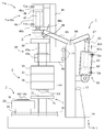
- FIG. 1 is a schematic view showing the whole of an example embodying the present invention.
- a bonding apparatus 1 according to the present invention includes a stage unit 2, a head unit 3, a head lifting mechanism 4, a head vibration unit 5, a chip supply unit 7, a bonding region observation unit 8, and a heater unit. It is configured.
- the stage unit 2 is configured to place the substrate W to be bonded to the device chip in the horizontal direction.
- the stage unit 2 is configured to include a substrate mounting table 20 in which the substrate holding force does not act when the substrate W is placed or replaced, and the substrate holding force acts after the substrate is placed.
- the stage unit 2 may be attached to the apparatus frame 10 if it is not necessary to move.
- the stage unit 2 be configured to be movable in the Y direction as shown in FIG.
- a pair of rails 25 extending in the Y direction are arranged on the apparatus frame 10, and a Y-axis slider 26 that moves on the rails 25 in the Y direction is provided.
- a Y-axis slider drive mechanism (not shown) is provided that moves the Y-axis slider 26 in a predetermined direction at a predetermined speed and stops at a predetermined location based on an external control signal.
- examples of the Y-axis slider drive mechanism include those in which the Y-axis slider 26 is driven by a rotary motor and a ball screw, those that are driven by a linear motor, and those that are driven by an air cylinder or a hydraulic cylinder. If it does so, the place where the board
- the chip supply unit 7 is in a state corresponding to the positions and intervals of the electrode pads P1 to P4 on the substrate W, A plurality of device chips C1 to C4 to be bonded onto these electrode pads P1 to P4 are supplied.
- the chip supply unit 7 includes a chip supply base 71 on which a plurality of device chips C1 to C4 are placed.
- the chip supply base 71 has a recess 72 corresponding to the outer shape of the device chips C1 to C4, and the depth of the recess 72 is larger than the thickness of the device chips C1 to C4. It is set shallowly.
- the positions and intervals of the recesses 72 are arranged in accordance with the positions and intervals of the electrode pads P1 to P4 of the substrate W. Therefore, the device chips C1 to C4 are dropped into the recesses 72 of the chip supply base 71, and are arranged in an aligned manner with the surface of each chip being above the surface of the chip supply base 71.
- the chip supply unit 7 is disposed at a position where it does not physically interfere with the stage unit 2.
- FIG. 1 shows a state in which the stage unit 2 is arranged on the front side and the chip supply unit 7 is arranged on the back side (the same applies to FIG. 3 described later).
- the chip supply unit 7 is not limited to the chip supply base 71 having a recess, and may be in another form.
- a chip positioning member such as a reference pin or a reference bar along the outer shape of the device chips C1 to C4 is arranged on a flat chip supply base. These chip positioning members are arranged so that each chip is in a state corresponding to the position / interval of the electrode pads P1 to P4 on the substrate W by aligning the device chips C1 to C4.
- the chip supply unit 7 may be configured to include a flat chip supply table and a chip mounter that aligns and arranges the device chips C1 to C4 at predetermined positions and intervals. That is, the electrode pads P1 to P4 are arranged on the flat chip supply table in a state corresponding to the positions and intervals of the electrode pads P1 to P4 of the substrate W.
- the device chips C1 to C4 can be arranged in advance in a state corresponding to the positions and intervals of the electrode pads P1 to P4 on the substrate W. . Therefore, these chips can be picked up at once using the head unit 3 and can be bonded onto the electrode pads P1 to P4 of the substrate W with a predetermined position and interval.
- the chip supply unit 7 may be provided in the bonding apparatus 1 according to the present invention, but is not an essential component.
- a chip transfer mechanism (so-called chip slider) incorporated in a chip transfer / transfer apparatus adjacent to the bonding apparatus 1 may be used. Then, the device chip can be supplied and picked up by interlocking the operation of the chip slider and the head unit 3.
- the head unit 3 holds a plurality of device chip chips C1 to C4 to be bonded on the substrate W at a time.
- the head unit 3 includes a chip holding unit 31 and a heater unit 32.
- the chip holding unit 31 holds a plurality of device chip chips C1 to C4.
- the chip holding unit 31 picks up the device chips C1 to C4 and applies a holding force until they are bonded to the substrate W, and does not apply a holding force until the next device chip is picked up after raising the head after bonding. Keep it as
- the chip holding part 31 is provided with a groove or a hole on the surface thereof and inside the outer shape of the device chips C1 to C4 to be picked up. These grooves and holes are connected to an external vacuum generation mechanism (not shown) via a switching valve (not shown) and the like so that they can be switched between a vacuum state and an atmospheric release state. By doing so, the chip holding unit 31 can appropriately hold and release the device chips C1 to C4 by suction.
- the substrate mounting table 20 of the stage unit 2 the chip mounting table 71 of the chip supply unit 7, and the chip holding unit 31 of the head unit 3 are adjusted in advance so as to be parallel to each other.
- the heater unit 32 heats the bonding paste CP for bonding the electrode pads P1 to P4 and the device chips C1 to C4.
- the heater unit 32 can be configured using a ceramic heater, a sheathed heater, or the like, so that heating ON / OF can be switched or the heating temperature can be set by voltage or voltage control from the outside. deep. With this configuration, the heater unit 32 provided in the head unit 3 can heat the bonding paste CP via the plurality of device chip chips C1 to C4.
- FIG. 2 is a schematic diagram showing a main part of an example of a form embodying the present invention.
- FIG. 2 shows the substrate mounting table 20 of the stage unit 2, the chip holding unit 31 and the heater unit 32 of the head unit 3, and the device chips C 1 to C 4 held on the lower surface of the chip holding unit 31. Furthermore, a substrate W to be handled as a bonding target by the bonding apparatus 1 according to the present invention is mounted on the substrate mounting table 20.
- the substrate W treated as a bonding target in the bonding apparatus 1 according to the present invention has a bonding paste CP applied in advance on the electrode pads P1 to P4 formed on the surface thereof. Further, the bonding paste CP is applied with a predetermined thickness (that is, a necessary amount) inside the outer shape of the electrode pads P1 to P4 by, for example, screen printing in consideration of the pressure at the time of bonding.
- the head elevating mechanism 4 moves the head unit 3 up and down with respect to the stage unit 2 and the chip supply unit 7.
- the head unit 3 is attached to a Z-axis slider 43 that is a movable member of the head lifting mechanism 4.
- FIG. 3 is a schematic view showing the whole of an example embodying the present invention.
- FIG. 1 shows a state where the Z-axis slider 43 and the head unit 3 of the head lifting mechanism 4 are raised
- FIG. 3 shows a state where the Z-axis slider 43 and the head unit 3 are lowered.
- the head lifting mechanism 4 includes a base plate 41, a pair of rails 42 arranged on the base plate 41 and extending in the Z direction, and a Z-axis slider 46 that moves on the rails 42 in the Z direction.
- a rotation motor 45 is attached to the Z-axis slider 43 via a ball screw 44.
- the rotation motor 45 can rotate at a predetermined rotation speed in a predetermined direction based on a control signal from the outside, and can stop at a predetermined angle. Therefore, based on signal control from the outside, the Z-axis slider 43 can be moved at a predetermined speed in a predetermined direction and can be stopped at a predetermined location.
- the head portion 3 is attached to the Z-axis slider 43 through connecting members 33, 34, and 35 as appropriate. Therefore, the head unit 3 can move up and down in the vertical direction based on a control signal from the outside, and can be stationary at a predetermined position.
- the head elevating mechanism 4 is not limited to the form using the rotary motor as described above, and the Z-axis slider 43 may be moved up and down using an air cylinder or a hydraulic cylinder.
- the head elevating mechanism 4 may be fixedly attached to the apparatus frame 10 via the base plate 41 or the connecting member 11 if it is not necessary to move the head unit 3 in the horizontal direction.
- the above-described chip supply unit 7 includes a mechanism for moving the chip mounting table 71 to a position below the head unit 3 and waiting in that state while maintaining a state in which the chip supply unit 7 does not physically interfere with the stage unit 2. Keep it in configuration.
- the head lifting mechanism 4 is preferably configured to be movable in the X direction as shown in FIGS.
- a pair of rails 15 extending in the X direction are arranged on the connecting member 11, the X axis slider 16 moving in the X direction on the rail 15 is provided, and the base plate 41 is attached to the X axis slider 16.
- An X-axis slider drive mechanism (not shown) is provided that moves the X-axis slider 16 at a predetermined speed and stops it at a predetermined location based on a control signal from the outside.
- examples of the X-axis slider drive mechanism include those in which the X-axis slider 16 is driven by a rotary motor and a ball screw, those that are driven by a linear motor, and those that are driven by an air cylinder or a hydraulic cylinder. By doing so, it is possible to individually set a place where the head unit 3 picks up the device chips C1 to C4 and a place where the chip devices C1 to C4 are bonded to the substrate W.
- the head vibration unit 5 vibrates the head unit 3 in the vertical direction.
- the head excitation unit 5 can be exemplified by a high-frequency vibration generator 51 or the like, and is attached to the connecting member 35 to which the head unit 3 is attached via the connecting members 33 and 34.
- the high frequency vibration generator 51 vibrates appropriately with a predetermined amplitude and frequency based on an external control signal. More specifically, the high-frequency vibration generator 51 includes a rotary motor therein, and the eccentric weight attached to the rotary motor rotates to generate vibration in the direction indicated by the arrow 52. . Alternatively, the high-frequency vibration generator 51 may generate a vibration in the direction indicated by the arrow 52 when a vibrator having a predetermined weight reciprocates.
- the bonding paste CP used for bonding the device chip has a high viscosity, so that it is difficult to spread it even by simple press. That is, it is difficult to spread the bonding paste CP thinly while keeping the thickness of the bonding paste CP uniform at the central portion and the peripheral portion of the region where the bonding paste CP is applied. Therefore, the bonding paste is further applied by applying vibration after bringing the device chips C1 to C4 before bonding into contact with the bonding paste CP applied on the electrode pads P1 to P4. The distance between the device chips C1 to C4 and the electrode pads P1 to P4 can be reduced while pushing the CP uniformly and thinly. Therefore, it can be said that the bonding apparatus 1 according to the present invention is a suitable form for bonding a plurality of device chips to the substrate W coated with the high-viscosity bonding paste CP.
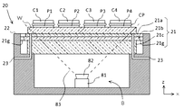
- FIG. 4 is a cross-sectional view showing a main part of an example embodying the present invention, in which the substrate mounting table 20 of the stage unit 2 and the bonding region observation unit 8 incorporated therein are shown.
- the substrate mounting table 20 among the supporting members that support the substrate W, at least the outer peripheral portions of the plurality of device chips to be bonded and the portions corresponding to the outer sides thereof are made of a transparent body.
- the substrate mounting table 20 includes a support member 21, a frame member 22, and a suction portion 23.
- the support member 21 touches the substrate W and directly supports the substrate W.
- the support member 21 includes a protective plate 21a, a heater portion 21b, a reinforcing plate 21c, and a heat insulating portion 21g.
- the protective plate 21a is in direct contact with the substrate W and transmits heat energy generated by the heater 21b to the substrate W. Moreover, the heater part 21b and the board
- the heater unit 21b is for heating the substrate W.
- the reinforcing plate 21 c is for preventing the heat energy generated by the heater portion 21 b from escaping to the frame member 22 while ensuring the strength of the support member 21.
- the heat insulating portion 21g is for preventing the heat energy generated by the heater portion 21b from escaping to the frame member 22.
- the protective plate 21a and the reinforcing plate 21c are made of glass plates.
- the heater unit 21b includes a glass plate and a transparent electrode such as ITO or IZO formed on the surface thereof.
- the heater unit 21b generates heat due to the internal resistance of the transparent electrode by applying current and voltage to the transparent electrode. Then, voltage or voltage control is performed on the transparent electrode from an external power source (not shown) so that heating ON / OF can be switched and the heating temperature can be set.
- the heat insulating portion 21g is made of a material having both heat resistance and heat insulating properties such as silica and alumina, and is arranged between the outer edge portion of the heater portion 21b and the frame member 22 with a predetermined width and thickness. Therefore, the outer edge part of the heater part 21b does not touch the frame member 22 directly.
- the heater portion 21b can heat the bonding paste CP via the protective plate 21a, the substrate W, and the plurality of electrode pads P1 to P4.
- the support member 21 may be formed of a single-layer glass plate when the heater portion is not incorporated.
- the frame member 22 supports the support member 21.
- the frame member 21b is configured by a box or a frame-like housing having an opening on the upper surface.
- the suction unit 23 is a communication port for sucking the substrate W.
- the adsorbing portion 23 is configured to penetrate the support member 21 and the frame member 22 in a portion inside the outer peripheral portion of the substrate W to be placed and communicate with the outside. More specifically, the adsorbing unit 23 is connected to an external vacuum generation mechanism (not shown) via a switching valve (not shown) or the like so that it can be switched between a vacuum state and an atmospheric release state.
- the protective plate 21a may be provided with a groove having a predetermined pattern so that the substrate W can be efficiently suctioned ON / OFF.
- the material used for the above-described support member 21 is not limited to a glass plate, and may be any material that transmits the wavelength of observation light from the bonding region observation unit 8. That is, if the observation light is visible light, a narrowly defined transparent body such as an acrylic resin, a PET resin, or a polycarbonate resin can be selected. On the other hand, if the observation light is near infrared, a transparent material in a broad sense such as a ceramic material through which the near infrared passes can be selected.
- the bonding region observation unit 8 is for observing a region including at least the peripheral portions of the device chips C1 to C4 bonded onto the electrode pads P1 to P4. If the electrode pads P1 to P4 are transparent, the bonding region observation unit 8 observes so as to include a region inside the outer edge of the bonding paste CP. If the electrode pads P1 to P4 are non-transparent such as metal For example, it is observed so as to include at least a region outside the peripheral portion of the electrode pads P1 to P4 and inside the outer edge portion of the bonding paste CP that protrudes outward from the peripheral portion.
- the bonding region observation unit 8 is configured by combining an area sensor camera 81 having an imaging element such as a CCD or CMOS and an imaging lens 82, and each electrode pad P1 to P4, its peripheral portion, and its outside.
- the angle of view is set so that the area can be observed at once.
- the bonding region observation unit 8 is disposed to face the head unit 3 so as to sandwich the support member 21 of the stage unit 2. That is, the area sensor camera 81 includes the electrode pads P1 to P4 of the substrate W arranged on the support member 21, the bonding paste CP applied thereon, and the device chips C1 to C1 that are in close contact therewith. Focusing around C4, it is arranged to observe them. The area sensor camera 81 can observe the area inside the angle of view represented by the alternate long and short dash line 83.
- the area sensor camera 81 can process the captured image and output it as an image signal to the outside.
- the image signal here means an analog video signal such as NTSC or PAL, or a digitally encoded video signal.
- the paste state inspection unit 9 inspects the state of the bonding paste CP in contact with the plurality of device chips C1 to C4 based on the image signal corresponding to the image observed by the bonding region observation unit 8.
- the state of the bonding paste CP refers to a protruding state or a curing reaction state of the bonding paste CP. That is, when the plurality of device chips C1 to C4 are bonded to the electrode pads P1 to P4 by pressing and heating, whether or not the bonding paste CP protrudes around the device chips C1 to C4, The protruding state of whether or not the pads P1 to P4 are protruding and the protruding dimension of the bonding paste CP is inspected. Alternatively, the state of discoloration of the bonding paste CP is examined, and the paste curing reaction state is checked to determine whether or not a predetermined bonding strength can be exhibited.
- the paste state inspection unit 9 can be configured by an image processing device 91 and an image processing program incorporated therein.
- the image processing apparatus 91 includes an image signal acquisition unit 93.
- the image signal acquisition unit 93 acquires the image signal output from the bonding region observation unit 8.
- the image processing device 91 restores the image signal acquired by the image signal acquisition unit 93 and restores the image observed by the joint region observation unit 8. Furthermore, the image processing apparatus 91 can perform various paste state inspections as described below based on an image processing program incorporated in advance.
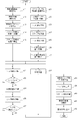
- FIG. 5 is a flowchart showing an example of a form embodying the present invention.
- a substrate W on which bonding paste is applied to the electrode pads P1 to P4 is placed on the stage unit 2 (s11).
- the bonding device chips C1 to C4 are arranged side by side aligned in a predetermined position and direction (s21).
- the stage unit 2 is sucked and held (s12), the position alignment of the substrate W is performed (s13), the stage unit 2 is moved to the bonding position (s14), and is stopped (s15).
- the head unit 3 is moved to a predetermined position above the chip supply unit 7 (s22), the head unit 3 is lowered (s23), and the device chips C1 to C4 are moved.
- C4 is vacuum-sucked (s24), the head unit 3 is raised again (s25), the head unit 3 is moved to the joining position (s26), and is put on standby above the stage unit 3 (s27).
- the head 3 is lowered (s31).
- the head unit 3 is lowered, and it is determined whether or not the device chips C1 to C4 are in contact with the bonding paste CP applied on the electrode pads P1 to P4 of the substrate W (s32). Note that this contact determination is made based on a rise in the current value of the rotary motor, a determination based on a decrease in the position of the Z-axis slider or the position change amount, or a pressure sensor incorporated in advance in the stage unit 2 or the head unit 3. It is possible to make a determination based on the signal output.
- the head vibration unit 5 When it is determined that the device chips C1 to C4 are in contact with the bonding paste CP applied on the electrode pads P1 to P4 of the substrate W, the head vibration unit 5 is operated to apply the bonding paste CP. Spread thinly and uniformly (s34).
- the heater unit is operated (s35), and the device chips C1 to C4 and the electrode pads P1 to P4 are joined.
- the vacuum suction of the head part 3 and the head vibration part / heater part are changed from the operating state to the stopped state (s38).
- the part 3 is raised (s39).
- the stage unit 2 is moved to the substrate replacement position (s40), the adsorption state of the substrate is released (s41), and the substrate to which the device chips C1 to C4 are bonded is taken out (s42).
- the bonding apparatus 1 further includes a control unit for controlling each of the above-described devices, semi-automatically with human intervention, or presetting bonding operation and various conditions, and based on a program. Automatically, the series of bonding operations described above (s11 to s42) I do.
- the bonding apparatus 1 Since the bonding apparatus 1 according to the present invention has the above-described configuration, the plurality of device chips C1 to C4 are simultaneously bonded onto the plurality of electrode pads P1 to P4 provided on the surface of the substrate W. However, the state of the bonding paste CP can be inspected.
- the paste state inspection unit 9 causes the image processing program incorporated in the image processing apparatus 91 to perform the following inspection.
- FIG. 6 is an image view showing a main part of the embodiment embodying the present invention, and shows an image image in which the bonding area observation unit 8 looks up the substrate W from the lower surface side.
- the paste state inspection unit 8 measures the protruding dimensions d1 to d8 of the bonding paste CP protruding from the electrode pad P1.
- the protruding dimensions d1 to d8 mean dimensions protruding from the peripheral portions of the respective sides of the device chips C1 to C4.
- there are a total of 8 locations for measuring the protruding dimensions for the corners and ridges but they may be further subdivided.
- the protruding dimension of the bonding paste CP is measured in the same manner as described above.
- the bonding paste CP that protrudes from the electrode pads P1 to P4 is previously associated with the color, the degree of shading, and the cured state, and an image observed during heat-curing is acquired and subjected to image processing. It is determined whether the curing has progressed, and the curing reaction state of the paste is inspected.
- the substrate W is made of a transparent material and the electrode pads P1 to P4 are made of transparent electrodes, and the entire bonding paste CP is observed through the substrate W to inspect the curing reaction state.
- FIG. 7 is a characteristic diagram showing the bonding strength and observation luminance of the bonding paste used in the present invention, illustrating the change in the curing reaction state of the bonding paste CP and the corresponding change in the observation luminance.
- FIG. 7 shows the heating time on the horizontal axis and the bonding strength and observation luminance of the bonding paste CP on the vertical axis.
- the bonding paste CP exemplified here, the binder component volatilizes as the heating proceeds, and the bonding strength gradually increases as the metal particles are bonded to each other.
- the bonding paste CP has an observation luminance of 60% when the bonding strength Ta is necessary for bonding the device chips, and further has an observation luminance of 80% when the bonding strength Tb is reached. If the heating is further continued, the strength is slightly increased. However, if the heating is excessive, the bonding strength is lowered.
- the bonding strength of the bonding paste CP can be inspected in advance, and the bonding strength can be inspected by measuring the observation luminance. That is, the paste state inspection unit 9 can inspect the reaction state of the bonding paste CP.
- the paste state inspection unit 9 is not limited to the above-described inspection items, and whether or not bubbles are generated or mixed during the pressurization / vibration / heating of the bonding paste CP. You may inspect.
- the substrate W is a transparent body, and the electrode pads P1 to P4 are made of transparent electrodes.
- the bonding apparatus according to the present invention is provided with a protrusion allowable range setting section for the above-described paste protrusion dimension inspection, and the paste state inspection section 9 includes a bonding paste protruding from the outer peripheral portions of the plurality of device chips C1 to C4. It is good also as a structure which test
- the protrusion allowable range setting unit sets the protrusion allowable range for the protrusion dimension of the bonding paste CP protruding from the outer peripheral portion of the plurality of device chips C1 to C4.
- the allowable protrusion range of the paste is set to 0.1 to 0.3 mm. In this way, it is determined whether or not a protrusion of 0.1 mm or more has occurred at least in a place where the protrusion is small, and a clearance of 0.4 mm or more between adjacent electrodes is secured in a place where the protrusion is large. It is possible to determine whether or not it is inspected.
- the bonding apparatus may be configured such that when the protrusion allowable range is set for the above-described inspection of the paste protrusion size, the paste state inspection unit 9 notifies the outside if the inspection result is abnormal.
- the paste state inspection unit 9 measures the protrusion size of the bonding paste CP for each of the electrode pads P1 to P4, and if at least one of them is out of the allowable range of protrusion, the inspected bonding material Notifies that the protruding size of the paste is abnormal.
- any of the protruding dimensions measured for each of the electrode pads P1 to P4 is 0. If it exceeds 3 mm, or if any of the protruding dimensions is less than 0.1 mm, it notifies the outside that the protruding dimensions are abnormal.
- This abnormality notification means notification based on a change in signal level connected to an external device, and visual / auditory notification to an operator using a lamp or a buzzer.
- the bonding apparatus may further include a protruding allowable upper limit setting unit and a control unit when performing the above-described inspection of the protruding size of the paste.
- the protrusion allowable upper limit setting section sets a protrusion allowable upper limit for the protrusion dimension of the bonding paste CP protruding from the outer peripheral portion of the electrode pads P1 to P4.
- the control unit 95 raises the head unit 3 or the heater unit 21b. The heating of the heater part 32 is stopped.
- the control unit 95 is connected to the heater unit 21 b of the stage unit 2, the heater unit 32 of the head unit 3, the rotary motor 45 of the head lifting mechanism 4 that moves the head unit 3 up and down, and the paste state inspection 9. Based on the inspection result, other connected devices are controlled.
- the control unit 95 performs the following control. That is, 1) The rotation of the rotary motor 45 of the head elevating mechanism 4 is stopped and further rotated in the reverse direction to raise the head unit 3. 2) The heating unit 21b of the stage unit 2 and the temperature control unit of the heater unit 32 of the head unit 3 are controlled to lower the heating temperature or stop heating.
- the bonding apparatus includes a curing reaction state allowable range setting unit in the above-described inspection of the curing reaction state of the paste.
- the curing reaction state of the bonding paste CP is the curing reaction state. It is good also as a structure which test
- the curing reaction state allowable range setting unit sets the allowable range of the curing reaction state for the curing reaction state of the bonding paste CP.
- an observation luminance of 60% to 80% corresponding to the bonding strengths Ta and Tb of the bonding paste CP is set as an allowable range of the curing reaction state.
- the paste state inspection unit 9 when the bonding apparatus according to the present invention sets the allowable range of the curing reaction state for the above-described inspection of the curing reaction state of the paste, the paste state inspection unit 9 notifies the outside if the inspection result is abnormal. Also good. In this case, the paste state inspection unit 9 measures the curing reaction state of the bonding paste CP for each of the electrode pads P1 to P4, and if at least one of them is outside the allowable range of the curing reaction state, Notify that the curing reaction state of the inspected bonding paste is abnormal.
- the bonding paste CP of the electrode pads P1 to P4 Among these, if any observation luminance exceeds 80% or any observation luminance is less than 60%, the outside is notified that the reaction state of the bonding paste CP is abnormal.
- This abnormality notification means notification based on a change in signal level connected to an external device, and visual / auditory notification to an operator using a lamp or a buzzer.
- the bonding apparatus may be configured to further include a curing reaction state allowable upper limit setting unit and a control unit when inspecting the curing reaction state of the above-described bonding paste CP.
- the curing reaction state allowable upper limit setting unit sets an allowable upper limit of the curing reaction state of the bonding paste CP.
- the control unit 95 raises the head unit 3 or stops heating the heater units 21b and 32. is there.
- the control unit 95 is connected to the heater unit 21 b of the stage unit 2, the heater unit 32 of the head unit 3, the rotary motor 45 of the head lifting mechanism 4 that moves the head unit 3 up and down, and the paste state inspection 9. Based on the inspection result, other connected devices are controlled.
- the control unit 95 performs the following control. That is, 1) The rotation of the rotary motor 45 of the head elevating mechanism 4 is stopped and further rotated in the reverse direction to raise the head unit 3. 2) The heating unit 21b of the stage unit 2 and the temperature control unit of the heater unit 32 of the head unit 3 are controlled to lower the heating temperature or stop heating.
- the head elevating mechanism 4 and the head exciting unit 5 are not limited to the configuration described above with reference to FIGS. It is good also as 4a and the head vibration part 5a.
- FIG. 8 and 9 are schematic views showing the whole of another example of a form embodying the present invention. 8 shows a state in which the head unit 3 is raised, and FIG. 9 shows a state in which the head unit 3 is lowered.
- a bonding apparatus 1a includes a stage part 2 and a head part 3 having the same configuration as the bonding apparatus 1, and a head lifting / lowering part 4a having a different configuration.
- the head elevating mechanism 4a moves the head unit 3 up and down with respect to the stage unit 2.
- the connecting member 36 of the head unit 3 is attached to a shaft 47 which is a movable side member of the head lifting mechanism 4a via a spherical bearing S.
- the head elevating mechanism 4a is constituted by a linear cylinder unit 40a attached to the base plate 41.
- the linear cylinder unit 40a includes a housing 46, a shaft 47, and pressurized fluid supply ports 46a and 46b for taking the shaft 47 in and out.
- the casing 46 is hollow and sealed inside, and a valve plate 48 connected to the shaft 47 is provided in the casing 46 due to a pressure difference between the fluids supplied to the pressurized fluid supply ports 46a and 46b. Is configured to reciprocate.
- the pressure f1a on the pressurized fluid supply port 46a side of the linear cylinder unit 40a is smaller than the pressure f1b on the pressurized fluid supply port 46b side (for example, the pressurized fluid supply port 46a side is connected to the atmosphere). If it is released and compressed air is supplied to the pressurized fluid supply port 46b), the shaft 47 and the head portion 3 are raised as shown in FIG.
- the pressure f1a on the pressurized fluid supply port 46a side of the linear cylinder unit 40a becomes larger than the pressure f1b on the pressurized fluid supply port 46b side (for example, compressed air is supplied to the pressurized fluid supply port 46a side).
- the shaft 47 and the head part 3 are lowered to the stage part 2 side as shown in FIG.
- the base plate 41 is provided with an elevating guide part 49 so that the vertical movement of the head part 3 is smoothed and no shaking occurs in the horizontal direction.
- the raising / lowering guide part 49 is comprised including the shaft 49s and the linear bush 49b.
- the head vibration unit 5a vibrates the head unit 3 in the vertical direction by repeating the lifting operation of the head lifting mechanism 4a with the head unit 3 lowered to the stage unit 2 side.
- the head vibration unit 5a can be realized by switching the reciprocating operation of the linear cylinder unit 40a of the head lifting mechanism 4a at high speed.
- the bonding apparatus 1a may be configured to further include a head pressure unit 6.
- the head pressurization unit 6 further pressurizes the head unit 3 toward the stage unit 2 side.
- the head pressurizing unit 6 can be configured as shown in FIGS. That is, the head pressurization unit 6 further presses the shaft 49a, which is a movable member for moving the head unit 3 in the vertical direction, to the stage unit 2 side via the connecting member 33 attached to the head unit 3. It has a configuration with a mechanism.
- the head pressure unit 6 includes a linear cylinder unit 60 and a pressing member 65.
- the linear cylinder unit 60 includes a housing 61, a shaft 62, and pressurized fluid supply ports 61a and 61b for taking the shaft 62 in and out.
- the casing 61 is hollow with its inside sealed, and a valve plate 63 connected to the shaft 62 is formed in the casing 61 by the pressure difference between the fluids supplied to the pressurized fluid supply ports 61a and 61b. Is configured to reciprocate.
- the holding member 65 has a linear shape or a substantially L shape (including a substantially V shape), and is attached to the connecting member 11 of the apparatus frame 10 via a knuckle joint 66.
- the pressing member 65 is configured such that the tip portion 68 rotates in the vertical direction around the shaft portion of the knuckle joint 66 as the shaft 62 reciprocates.
- the pressure f2a on the pressurized fluid supply port 61a side of the linear cylinder unit 60 becomes larger than the pressure f2b on the pressurized fluid supply port 61b side (for example, compressed to the pressurized fluid supply port 61a side). If air is supplied and the pressurized fluid supply port 61b side is released to the atmosphere), as shown in FIG. 5, the shaft 62 is lowered in the direction indicated by the arrow 62v, and the tip 68 of the pressing member 65 is It will be in the state raised to the direction shown to 68v. In this state, the distal end portion 68 is separated from the connecting member 36 connected to the head 3, and the pressing force for pressing the head portion 3 against the stage portion 2 side does not act.
- the pressure f2a on the pressurized fluid supply port 61a side of the direct acting cylinder unit 60 is smaller than the pressure f2b on the pressurized fluid supply port 62b side (for example, the pressurized fluid supply port 61a side is released to the atmosphere, 6), the shaft 62 rises in the direction indicated by the arrow 62v, and the distal end portion 68 of the pressing member 65 is indicated by the arrow 68v. It will be in a state of descending in the direction. In this state, the distal end portion 68 presses the connecting member 36 connected to the head 3, and a pressing force that presses the head portion 3 against the stage portion 2 side acts.
- the bonding apparatus including the head pressurizing unit 6 has the device chip after the bonding paste CP is pushed and expanded by the head lifting / lowering operation and the head vibrating unit.
- the distance between C1 to C4 and the electrode pads P1 to P4 can be maintained.
- the device chips C1 to C4 can be further pushed into the substrate W side to slightly close the distance from the electrode pads P1 to P4.
- the head pressure unit 6 uses the point where the tip 68 of the pressing member 65 contacts the connecting member 36 as an action point of the pressing force, and the head part 3 is placed on the stage part 2 at the action point on the connecting member 36. It has a structure in which the force of pressing toward the side works. For this reason, even if the force for pushing the head unit 3 by the head pressurizing unit 3 is set large, the pressure can be applied without depending on the vertical movement of the head elevating unit 4. By doing so, it is possible to prevent extra stress from being applied to the X-axis slider 15 and the linear motion guide portion of the head elevating mechanism 4 as occurs when the pressure is applied only by the head elevating unit 4.
- the device chips C1 to C4 are heated in order to bond the device chip and the electrode pad while maintaining the parallelism between the stage unit 2 and the head unit 3, and the solvent of the bonding paste CP is volatilized to reduce the volume.
- the bonding can be completed in a state where the bonding paste CP is spread over the entire contact area.
- the bonding apparatus 1a has a configuration including such a head pressure unit 6 and is combined with a protrusion inspection of the bonding paste CP or a reaction state inspection, and the head is added according to the inspection results. It is good also as a structure which stops the pressurization by the pressure part 6.
- a protrusion allowable upper limit setting unit for the bonding paste CP or a curing reaction state allowable upper limit setting unit for the bonding paste CP, and a control unit 95 are provided.
- the protrusion allowable upper limit value setting part and the curing reaction state allowable upper limit value setting part of the bonding paste CP can be exemplified by the same configuration as described above. Further, if the paste state inspection unit 9 determines that the bonding paste CP protruding from the outer peripheral portion of the electrode pads P1 to P4 has reached the protrusion allowable upper limit value, or the control unit 95, or the bonding paste CP If it is determined that the reaction state has reached the allowable upper limit value, the pressurization of the head pressurizing unit 6 is stopped.
- control unit 95 controls the pressure of the fluid supplied to the pressurized fluid supply ports 61a and 61b of the linear motion cylinder unit 60 based on the inspection result output from the paste state inspection unit 9.
- the shaft 62 is contracted to a state shown in FIG. 8 (that is, a state in which a force for pressing the head portion 3 downward is not applied).
Landscapes
- Engineering & Computer Science (AREA)
- Mechanical Engineering (AREA)
- Manufacturing & Machinery (AREA)
- Microelectronics & Electronic Packaging (AREA)
- Physics & Mathematics (AREA)
- Optics & Photonics (AREA)
- Electric Connection Of Electric Components To Printed Circuits (AREA)
- Die Bonding (AREA)
- Wire Bonding (AREA)
Abstract
Description
基板表面に設けられた複数の電極パッド上に、複数のデバイスチップを接合するボンディング装置であって、
前記基板を載置し支持するステージ部と、
前記複数の電極パッド上にボンディングする複数のデバイスチップを一度に保持するヘッド部と、
前記ステージ部に対して前記ヘッド部を上下方向に昇降移動させるヘッド昇降機構と、
前記ヘッド部を上下方向に加振するヘッド加振部と、
前記複数の電極パッドと各デバイスチップを接合する接合用ペーストを加熱するヒータ部と、
前記複数のデバイスチップが接合される各電極パッドの周辺部を少なくとも含む領域を観察する接合領域観察部とを備え、
前記ステージ部は、前記基板を支える支持部材のうち、前記複数のデバイスチップが接合される各電極パッドの周辺部及びその外側に対応する部分が、透明体で構成されており、
前記接合領域観察部は、前記ステージ部の前記支持部材を挟むように前記ヘッド部と対向配置されており、
前記接合領域観察部で観察した画像を画像信号として取得する画像信号取得部と、
前記画像信号に基づいて、前記複数のデバイスチップと接する接合用ペーストの状態を検査する、ペースト状態検査部を備えた、
ボンディング装置である。
前記ペースト状態検査部は、前記複数のデバイスチップの周囲からはみ出した接合用ペーストのはみ出し寸法を検査することを特徴とする。
前記複数の電極パッドの外周部からはみ出した前記接合用ペーストのはみ出し寸法について、はみ出し許容範囲を設定する、はみ出し許容範囲設定部を備え、
前記ペースト状態検査部は、前記複数の電極パッドの外周部からはみ出した前記接合用ペーストのはみ出し寸法が、前記はみ出し許容範囲内であるかどうかを検査することを特徴とする。
前記ペースト状態検査部は、前記複数の電極パッドのうち少なくとも1つについて、検査した接合用ペーストのはみ出し寸法が前記はみ出し許容範囲外であれば、当該検査した接合用ペーストのはみ出し寸法が異常であることを通知することを特徴とする。
前記複数の電極パッドの外周部からはみ出した前記接合用ペーストのはみ出し寸法について、はみだし許容上限値を設定する、はみ出し許容上限値設定部を備え、
前記ペースト状態検査部において前記複数の電極パッドの外周部からはみ出した前記接合用ペーストが前記はみ出し許容上限値に達したと判定されれば、前記ヘッド部を上昇させる又は前記ヒータ部の加熱を止める、制御部を備えた
ことを特徴とする。
前記ヘッド部を前記ステージ部側に向けてさらに加圧するヘッド加圧部と、
前記複数の電極パッドの外周部からはみ出した前記接合用ペーストのはみ出し寸法について、はみだし許容上限値を設定する、はみ出し許容上限値設定部を備え、
前記ペースト状態検査部において前記複数の電極パッドの外周部からはみ出した前記接合用ペーストが前記はみ出し許容上限値に達したと判定されれば、前記ヘッド加圧部の加圧を止める、制御部を備えたことを特徴とする。
前記ペースト状態検査部は、前記接合用ペーストの硬化反応状態を検査することを特徴とする。
前記接合用ペーストの硬化反応状態の許容範囲を設定する、硬化反応状態許容範囲設定部を備え、
前記ペースト状態検査部は、前記接合用ペーストが、前記硬化反応状態の許容範囲内であるかどうかを検査することを特徴とする。
前記ペースト状態検査部は、前記複数の電極パッドのうち少なくとも1つについて、検査した接合用ペーストが前記硬化反応状態の許容範囲外であれば、当該検査した接合用ペーストの硬化反応状態が異常であることを通知することを特徴とする。
前記接合用ペーストの硬化反応状態の許容上限値を設定する、硬化反応状態許容上限値設定部を備え、
前記ペースト状態検査部において前記接合用ペーストが前記硬化反応状態の許容上限値に達したと判定されれば、前記ヘッド部を上昇させる又は前記ヒータ部の加熱を止める、制御部を備えたことを特徴とする。
前記ヘッド部を前記ステージ部側に向けてさらに加圧するヘッド加圧部をさらに備え、
前記接合用ペーストの硬化反応状態の許容上限値を設定する、硬化反応状態許容上限値設定部を備え、
前記ペースト状態検査部において前記接合用ペーストが前記硬化反応状態の許容上限値に達したと判定されれば、前記ヘッド加圧部の加圧を止める、制御部を備えたことを特徴とする。
また各図においては、直交座標系の3軸をX、Y、Zとし、XY平面を水平面、Z方向を鉛直方向とする。特に、X方向は、矢印の方向を手前側、その逆方向を奥側と表現し、Y方向は、矢印の方向を右側、その逆方向を左側と表現し、Z方向は矢印の方向(重力上方)を上側、その逆方向を下側と表現する。
本発明に係るボンディング装置1は、ステージ部2と、ヘッド部3と、ヘッド昇降機構4と、ヘッド加振部5と、チップ供給部7と、接合領域観察部8と、ヒータ部を備えて構成されている。
これら電極パッドP1~P4の上にボンディングする複数のデバイスチップC1~C4を供給するものである。具体的には、チップ供給部7は、複数のデバイスチップC1~C4を載置する、チップ供給台71を備えて構成されている。より具体的な形態を例示すると、チップ供給台71は、デバイスチップC1~C4の外形と対応した凹み部72を有し、この凹み部72の深さは、デバイスチップC1~C4の厚みよりも浅く設定されている。さらにこの凹み部72の位置・間隔は、基板Wの電極パッドP1~P4の位置・間隔に合わせて配置されている。そのため、デバイスチップC1~C4は、チップ供給台71の凹み部72に落とし込まれ、かつ、各チップの表面がチップ供給台71の表面よりも上側にある状態で整列配置される。なお、チップ供給部7は、ステージ部2とは物理的に干渉しない位置に配置しておく。例えば、図1には、ステージ部2が手前側、チップ供給部7が奥側に配置さている様子が示されている(後述の図3も同じ)。
具体的には、ヒータ部32は、セラミックヒータやシーズヒータなどを用いて構成することができ、外部からの電圧や電圧制御により、加熱ON/OFを切り替えたり、加熱温度が設定できるようにしておく。このような構成をしているので、ヘッド部3に備えられたヒータ部32は、複数のデバイスチップチップC1~C4を介して接合用ペーストCPを加熱することができる。
図2には、ステージ部2の基板載置台20と、ヘッド部3のチップ保持部31とヒータ部32と、チップ保持部31の下面で保持されたデバイスチップC1~C4が示されている。さらに、基板載置台20上には、本発明に係るボンディング装置1で接合対象として扱う基板Wが載置されている。
図1は、ヘッド昇降機構4のZ軸スライダー43とヘッド部3が上昇した状態を示しており、図3は、Z軸スライダー43とヘッド部3が下降した状態を示している。
基板載置台20は、基板Wを支える支持部材のうち、接合される前記複数のデバイスチップの少なくとも外周部及びその外側に対応する部分が、透明体で構成されている。
フレーム部材21bは、上面に開口部を設けた箱体や額縁状の筐体で構成されている。
ヘッド部3が下降し、基板WにデバイスチップC1~C4を加圧する際に、基板Wが載置された支持部材21全体を下面側から支えるものである。
具体的には、吸着部23は、載置される基板Wの外周部より内側の部分に、支持部材21やフレーム部材22を貫通し、外部のへ連通する構成をしている。より具体的には、吸着部23は、外部の真空発生機構(図示せず)と切替バルブ(図示せず)などを介して接続し、真空状態と大気解放状態に切り替えできるようにしておく。さらに、保護板21aには、所定パターンの溝などを設けておき、基板Wを効率よく吸着ON/OFFできる構造としても良い。
図5は、本発明を具現化する形態の一例を示すフロー図である。
予めステージ部2には、電極パッドP1~P4に接合用ペーストが塗布された基板Wを載置しておく(s11)。また、デバイスチップ供給部には、接合用デバイスチップC1~C4を所定の位置・方向にアライメントされた状態で並べて配置しておく(s21)。
を行う。
以下に、本発明に係るペースト状態検査部について、詳細を述べる。ペースト状態検査部9は、画像処理装置91に組み込まれた画像処理プログラムが、下記の検査を実施するようにしておく。
これは、電極パッドP1~P4の外側に接合用ペーストCPがどの程度はみ出しているか、はみ出し寸法を検査するものである。基板Wを透明体としておけば、このような検査ができる。
例えば、ペースト状態検査部8は、図6に示すように、電極パッドP1からはみ出した接合用ペーストCPのはみだし寸法d1~d8を測定する。ここで、はみ出し寸法d1~d8は、デバイスチップC1~C4の各辺の周辺部からはみ出した寸法を意味する。ここでは、説明を簡単に行うため、はみ出し寸法を測定する箇所は、角部や稜部について計8カ所に設定しているが、さらに細分化して設定しても良い。なお、他の電極パッドP2~P4についても、上述と同様に接合用ペーストCPのはみだし寸法を測定する。
これは、電極パッドP1~P4とデバイスチップC1~C4とを接合する接合用ペーストCPの色や濃淡度合いから、硬化反応がどの程度進んでいるかを検査するものである。基板Wを透明体とし、電極パッドP1~P4からはみ出した接合用ペーストCPを観察する。接合用ペーストCPが、銀ナノ粒子とバインダーで構成されている場合、加熱硬化前は黒っぽい灰色をしているが、加熱が進み硬化すれば白っぽい灰色若しくは白色に変化する。そのため、電極パッドP1~P4からはみ出した接合用ペーストCPについて、色や濃淡の度合いと硬化状態とを予め紐付けしておき、加熱硬化中に観察した画像を取得し、画像処理してどの程度硬化が進んでいるかを判定し、ペーストの硬化反応状態を検査する。或いは、基板Wを透明体、電極パッドP1~P4を透明電極で構成し、接合用ペーストCP全体を基板W越しに観察して、硬化反応状態を検査する。
ペースト状態検査部9は、上述の検査項目に限らず、接合用ペーストCPを加圧・加振・加熱中に気泡が発生したり混入したりしないかどうかを検査しても良い。この場合、基板Wを透明体とし、電極パッドP1~P4を透明電極で構成しておく。
本発明に係るボンディング装置は、上述したペーストのはみ出し寸法の検査に際し、はみ出し許容範囲設定部を備え、ペースト状態検査部9には、複数のデバイスチップC1~C4の外周部からはみ出した接合用ペーストCPのはみ出し寸法が、はみ出し許容範囲の範囲内であるかどうかを検査する構成としても良い。はみ出し許容範囲設定部は、複数のデバイスチップC1~C4の外周部からはみ出した接合用ペーストCPのはみ出し寸法について、はみ出し許容範囲を設定するものである。
さらに本発明に係るボンディング装置は、上述のペーストのはみ出し寸法の検査についてはみ出し許容範囲を設定した場合、ペースト状態検査部9は、検査結果が異常であれば外部へ通知する構成としても良い。この場合、ペースト状態検査部9は、電極パッドP1~P4のそれぞれについて、接合用ペーストCPのはみ出し寸法を測定し、そのうち少なくとも1つについてはみ出し許容範囲の範囲外であれば、当該検査した接合用ペーストのはみ出し寸法が異常であることを通知する。
また、本発明に係るボンディング装置は、上述のペーストのはみ出し寸法の検査を行う上で、はみ出し許容上限値設定部と、制御部をさらに備えた構成としても良い。はみ出し許容上限値設定部は、電極パッドP1~P4の外周部からはみ出した接合用ペーストCPのはみ出し寸法について、はみだし許容上限値を設定するものである。
[別の形態]
本発明に係るボンディング装置は、上述したペーストの硬化反応状態の検査に際し、硬化反応状態許容範囲設定部を備え、ペースト状態検査部9には、接合用ペーストCPの硬化反応状態が、硬化反応状態の許容範囲の範囲内であるかどうかを検査する構成としても良い。硬化反応状態許容範囲設定部は、接合用ペーストCPの硬化反応状態について、硬化反応状態の許容範囲を設定するものである。
さらに本発明に係るボンディング装置は、上述のペーストの硬化反応状態の検査について硬化反応状態の許容範囲を設定した場合、ペースト状態検査部9は、検査結果が異常であれば外部へ通知する構成としても良い。この場合、ペースト状態検査部9は、電極パッドP1~P4のそれぞれについて、接合用ペーストCPの硬化反応状態を測定し、そのうち少なくとも1つについて硬化反応状態の許容範囲の範囲外であれば、当該検査した接合用ペーストの硬化反応状態が異常であることを通知する。
また、本発明に係るボンディング装置は、上述の接合用ペーストCPの硬化反応状態の検査を行う上で、硬化反応状態許容上限値設定部と、制御部をさらに備えた構成としても良い。硬化反応状態許容上限値設定部は、接合用ペーストCPの硬化反応状態の許容上限値を設定するものである。
なお、本発明の適用にあたり、ヘッド昇降機構4及びヘッド加振部5は、図1,3を用いて上述したような構成に限定されず、図8,9に示すような構成のヘッド昇降機構4a及びヘッド加振部5aとしても良い。
なお、図8は、ヘッド部3が上昇した状態を示しており、図9は、ヘッド部3が下降した状態を示している。
さらに、本発明に係るボンディング装置1aは、ヘッド加圧部6をさらに備えた構成としても良い。
具体的には、ヘッド加圧部6は、図8,9に示すような構成とすることができる。つまり、ヘッド加圧部6は、ヘッド部3に取り付けられた連結部材33を介して、ヘッド部3を上下方向に移動させるための可動側部材であるシャフト49aを、ステージ部2側にさらに押さえつける機構を備えた構成をしている。
上述の説明では、接合用ペーストCPを加熱するヒータ部21b,32が、ステージ部2とヘッド部3の双方に備えられている構成を例示した。そうすることで、接合のための加熱時間が短くて済むため、生産効率を向上させることができる。しかし、本発明を具現化する上では、この形態に限定されず、どちらか一方を備えた構成としても良い。
2 ステージ部
3 ヘッド部
4 ヘッド昇降機構
5 ヘッド加振部
6 ヘッド加圧部
7 チップ供給部
8 接合領域観察部
9 ペースト状態検査部
10 装置フレーム
11 連結部材
15 レール
16 X軸スライダー
20 基板載置台
21 支持部材(ガラスステージ)
21a 保護板
21b ヒータ部
21c 補強板
21g 断熱材
22 フレーム部材
23 吸着部
25 レール
26 Y軸スライダー
31 チップ保持部
32 ヒータ部
33 連結部材
34 連結部材
35 連結部材
35 連結部材
40 直動駆動ユニット
40a 直動シリンダーユニット
41 ベースプレート
42 レール
43 Z軸スライダー
44 ボールねじ
45 回転モータ
46 筐体
46a 加圧流体供給ポート
46b 加圧流体供給ポート
47 シャフト
48 弁板
49 昇降ガイド部
49s シャフト
49b リニアブッシュ
51 高周波振動発生器
52 矢印(加振方向)
60 直動シリンダーユニット
61 筐体
61a 加圧流体供給ポート
61b 加圧流体供給ポート
62 シャフト
62v 矢印(シャフト移動方向)
63 弁板
65 押さえ部材
66 ナックルジョイント
67 ナックルジョイント
68 先端部
68v 矢印(回動方向)
71 チップ載置台
72 凹み部
81 エリアセンサーカメラ
82 撮像用レンズ
83 一点鎖線(画角)
91 画像処理装置
95 制御部
S 球面軸受
W 基板
C1~C4 デバイスチップ
P1~P4 電極パッド
CP 接合用ペースト
Claims (11)
- 基板表面に設けられた複数の電極パッド上に、複数のデバイスチップを接合するボンディング装置であって、
前記基板を載置し支持するステージ部と、
前記複数の電極パッド上にボンディングする複数のデバイスチップを一度に保持するヘッド部と、
前記ステージ部に対して前記ヘッド部を上下方向に昇降移動させるヘッド昇降機構と、
前記ヘッド部を上下方向に加振するヘッド加振部と、
前記複数の電極パッドと各デバイスチップを接合する接合用ペーストを加熱するヒータ部と、
前記複数のデバイスチップが接合される各電極パッドの周辺部を少なくとも含む領域を観察する接合領域観察部とを備え、
前記ステージ部は、前記基板を支える支持部材のうち、前記複数のデバイスチップが接合される各電極パッドの周辺部及びその外側に対応する部分が、透明体で構成されており、
前記接合領域観察部は、前記ステージ部の前記支持部材を挟むように前記ヘッド部と対向配置されており、
前記接合領域観察部で観察した画像を画像信号として取得する画像信号取得部と、
前記画像信号に基づいて、前記複数のデバイスチップと接する接合用ペーストの状態を検査する、ペースト状態検査部を備えた、
ボンディング装置。 - 前記ペースト状態検査部は、前記複数のデバイスチップの周囲からはみ出した接合用ペーストのはみ出し寸法を検査する
ことを特徴とする、請求項1に記載のボンディング装置。 - 前記複数の電極パッドの外周部からはみ出した前記接合用ペーストのはみ出し寸法について、はみ出し許容範囲を設定する、はみ出し許容範囲設定部を備え、
前記ペースト状態検査部は、前記複数の電極パッドの外周部からはみ出した前記接合用ペーストのはみ出し寸法が、前記はみ出し許容範囲内であるかどうかを検査することを特徴とする、請求項2に記載のボンディング装置。 - 前記ペースト状態検査部は、前記複数の電極パッドのうち少なくとも1つについて、検査した接合用ペーストのはみ出し寸法が前記はみ出し許容範囲外であれば、当該検査した接合用ペーストのはみ出し寸法が異常であることを通知することを特徴とする、請求項3に記載のボンディング装置。
- 前記複数の電極パッドの外周部からはみ出した前記接合用ペーストのはみ出し寸法について、はみだし許容上限値を設定する、はみ出し許容上限値設定部を備え、
前記ペースト状態検査部において前記複数の電極パッドの外周部からはみ出した前記接合用ペーストが前記はみ出し許容上限値に達したと判定されれば、前記ヘッド部を上昇させる又は前記ヒータ部の加熱を止める、制御部を備えた
ことを特徴とする、請求項2~4のいずれかに記載のボンディング装置。 - 前記ヘッド部を前記ステージ部側に向けてさらに加圧するヘッド加圧部と、
前記複数の電極パッドの外周部からはみ出した前記接合用ペーストのはみ出し寸法について、はみだし許容上限値を設定する、はみ出し許容上限値設定部を備え、
前記ペースト状態検査部において前記複数の電極パッドの外周部からはみ出した前記接合用ペーストが前記はみ出し許容上限値に達したと判定されれば、前記ヘッド加圧部の加圧を止める、制御部を備えた
ことを特徴とする、請求項2~5のいずれかに記載のボンディング装置。 - 前記ペースト状態検査部は、前記接合用ペーストの硬化反応状態を検査する
ことを特徴とする、請求項1に記載のボンディング装置。 - 前記接合用ペーストの硬化反応状態の許容範囲を設定する、硬化反応状態許容範囲設定部を備え、
前記ペースト状態検査部は、前記接合用ペーストが、前記硬化反応状態の許容範囲内であるかどうかを検査することを特徴とする、請求項7に記載のボンディング装置。 - 前記ペースト状態検査部は、前記複数の電極パッドのうち少なくとも1つについて、検査した接合用ペーストが前記硬化反応状態の許容範囲外であれば、当該検査した接合用ペーストの硬化反応状態が異常であることを通知する
ことを特徴とする、請求項8に記載のボンディング装置。 - 前記接合用ペーストの硬化反応状態の許容上限値を設定する、硬化反応状態許容上限値設定部を備え、
前記ペースト状態検査部において前記接合用ペーストが前記硬化反応状態の許容上限値に達したと判定されれば、前記ヘッド部を上昇させる又は前記ヒータ部の加熱を止める、制御部を備えた
ことを特徴とする、請求項7~9のいずれかに記載のボンディング装置。 - 前記ヘッド部を前記ステージ部側に向けてさらに加圧するヘッド加圧部をさらに備え、
前記接合用ペーストの硬化反応状態の許容上限値を設定する、硬化反応状態許容上限値設定部を備え、
前記ペースト状態検査部において前記接合用ペーストが前記硬化反応状態の許容上限値に達したと判定されれば、前記ヘッド加圧部の加圧を止める、制御部を備えた
ことを特徴とする、請求項7~10のいずれかに記載のボンディング装置。
Priority Applications (2)
| Application Number | Priority Date | Filing Date | Title |
|---|---|---|---|
| US15/028,819 US9711483B2 (en) | 2013-11-07 | 2014-10-28 | Bonding apparatus |
| KR1020167011892A KR20160082997A (ko) | 2013-11-07 | 2014-10-28 | 본딩 장치 |
Applications Claiming Priority (2)
| Application Number | Priority Date | Filing Date | Title |
|---|---|---|---|
| JP2013231148A JP6272676B2 (ja) | 2013-11-07 | 2013-11-07 | ボンディング装置 |
| JP2013-231148 | 2013-11-07 |
Publications (1)
| Publication Number | Publication Date |
|---|---|
| WO2015068607A1 true WO2015068607A1 (ja) | 2015-05-14 |
Family
ID=53041389
Family Applications (1)
| Application Number | Title | Priority Date | Filing Date |
|---|---|---|---|
| PCT/JP2014/078542 Ceased WO2015068607A1 (ja) | 2013-11-07 | 2014-10-28 | ボンディング装置 |
Country Status (4)
| Country | Link |
|---|---|
| US (1) | US9711483B2 (ja) |
| JP (1) | JP6272676B2 (ja) |
| KR (1) | KR20160082997A (ja) |
| WO (1) | WO2015068607A1 (ja) |
Cited By (2)
| Publication number | Priority date | Publication date | Assignee | Title |
|---|---|---|---|---|
| US10939600B2 (en) | 2018-11-28 | 2021-03-02 | International Business Machines Corporation | Flux residue detection |
| TWI844321B (zh) * | 2022-03-30 | 2024-06-01 | 日商芝浦機械電子裝置股份有限公司 | 基板處理裝置 |
Families Citing this family (15)
| Publication number | Priority date | Publication date | Assignee | Title |
|---|---|---|---|---|
| JP6643577B2 (ja) * | 2016-06-01 | 2020-02-12 | パナソニックIpマネジメント株式会社 | 印刷装置および半田管理システム |
| KR102575546B1 (ko) * | 2016-12-06 | 2023-09-08 | 삼성디스플레이 주식회사 | 본딩 장치 및 이의 본딩 방법 |
| JP6329667B1 (ja) * | 2017-04-13 | 2018-05-23 | Ckd株式会社 | 部品実装システム及び接着剤検査装置 |
| KR102000079B1 (ko) * | 2017-07-19 | 2019-07-18 | 세메스 주식회사 | 다이 본딩 장치 |
| CN109637942B (zh) * | 2017-10-09 | 2021-02-05 | 上海微电子装备(集团)股份有限公司 | 键合头装置、键合方法及键合机台 |
| CN110132960B (zh) * | 2018-02-09 | 2021-12-14 | 飞旭电子(苏州)有限公司 | 电路板组件的检测方法 |
| JP7325965B2 (ja) * | 2018-03-26 | 2023-08-15 | 芝浦メカトロニクス株式会社 | 素子実装装置、素子実装装置の調整方法、及び素子実装方法 |
| JP6752250B2 (ja) * | 2018-03-28 | 2020-09-09 | 東レエンジニアリング株式会社 | ツール高さ調整装置およびこれを備えたチップ部品転写装置 |
| JP7153844B2 (ja) * | 2018-12-10 | 2022-10-17 | パナソニックIpマネジメント株式会社 | 部品実装装置および部品実装方法 |
| EP3792962A1 (en) * | 2019-09-12 | 2021-03-17 | Infineon Technologies AG | Method for monitoring a process of forming a sinterable connection layer by photometric measurements |
| KR102744383B1 (ko) | 2019-10-02 | 2024-12-18 | 삼성전자주식회사 | 기판 본딩 장치 |
| KR102582980B1 (ko) * | 2021-08-12 | 2023-09-26 | 주식회사 엠아이이큅먼트코리아 | 정밀 가압장치를 구비한 플립칩 레이저 본딩기 |
| CN113823578B (zh) * | 2021-09-26 | 2024-06-14 | 西安欣业科技发展有限公司 | 一种双排芯片引脚连锡的检测方法 |
| CN114466526A (zh) * | 2021-11-02 | 2022-05-10 | 深圳市智链信息技术有限公司 | 一种无线接收信号放大器的芯片固定装置 |
| CN118553647B (zh) * | 2024-07-23 | 2024-11-29 | 深圳市路远智能装备有限公司 | 一种碳化硅芯片加工设备及其制备方法 |
Citations (3)
| Publication number | Priority date | Publication date | Assignee | Title |
|---|---|---|---|---|
| JP2005142537A (ja) * | 2003-10-15 | 2005-06-02 | Bondotekku:Kk | 縦振接合方法及び装置 |
| JP2005161783A (ja) * | 2003-12-05 | 2005-06-23 | Murata Mfg Co Ltd | スクリーン印刷装置 |
| WO2006118018A1 (ja) * | 2005-04-28 | 2006-11-09 | Toray Engineering Co., Ltd. | フリップチップ実装ずれ検査方法および実装装置 |
Family Cites Families (40)
| Publication number | Priority date | Publication date | Assignee | Title |
|---|---|---|---|---|
| US4200393A (en) * | 1976-06-07 | 1980-04-29 | Tokyo Shibaura Elecric Co., Ltd. | Method of positioning a semiconductor member by examining it and a die bonding apparatus using the same |
| JPS52149070A (en) * | 1976-06-07 | 1977-12-10 | Toshiba Corp | Locating and inspecting method for semiconductor parts and die bonding device using the same |
| US4606492A (en) * | 1984-10-03 | 1986-08-19 | Eastman Kodak Company | Method and apparatus for soldering |
| JP2835983B2 (ja) * | 1990-10-31 | 1998-12-14 | 株式会社新川 | ボンデイングヘツド |
| US5420691A (en) * | 1991-03-15 | 1995-05-30 | Matsushita Electric Industrial Co., Ltd. | Electric component observation system |
| JP2635889B2 (ja) * | 1992-06-24 | 1997-07-30 | 株式会社東芝 | ダイボンディング装置 |
| US5555316A (en) * | 1992-06-30 | 1996-09-10 | Matsushita Electric Industrial Co., Ltd. | Inspecting apparatus of mounting state of component or printing state of cream solder in mounting line of electronic component |
| US5564183A (en) * | 1992-09-30 | 1996-10-15 | Matsushita Electric Industrial Co., Ltd. | Producing system of printed circuit board and method therefor |
| JP3295529B2 (ja) * | 1994-05-06 | 2002-06-24 | 松下電器産業株式会社 | Ic部品実装方法及び装置 |
| JP3034774B2 (ja) * | 1994-12-28 | 2000-04-17 | 株式会社カイジョー | ワイヤボンディング装置 |
| JPH08306715A (ja) | 1995-05-02 | 1996-11-22 | Rohm Co Ltd | 半導体チップのダイボンディング用導電性ペーストの塗布方法及びその装置 |
| SG71804A1 (en) * | 1995-08-30 | 2000-04-18 | Matsushita Electric Industrial Co Ltd | Screen printing method and screen printing apparatus |
| US5982927A (en) * | 1996-12-19 | 1999-11-09 | Cognex Corporation | Methods and apparatuses for in-line solder paste inspection |
| JP4346827B2 (ja) * | 2001-03-06 | 2009-10-21 | パナソニック株式会社 | 電子部品実装方法 |
| US7296727B2 (en) * | 2001-06-27 | 2007-11-20 | Matsushita Electric Industrial Co., Ltd. | Apparatus and method for mounting electronic components |
| DE60306389T2 (de) * | 2002-08-19 | 2006-10-19 | Matsushita Electric Industrial Co., Ltd., Kadoma | Verfahren zur Bildung von Druckkontrolldaten |
| WO2004063733A1 (en) * | 2003-01-09 | 2004-07-29 | Matsushita Electric Industrial Co., Ltd. | Image recognition apparatus and image recognition method |
| EP1724050B1 (en) * | 2004-03-09 | 2013-12-04 | Senju Metal Industry Co., Ltd. | Solder paste |
| JP4493421B2 (ja) * | 2004-06-30 | 2010-06-30 | 株式会社リコー | プリント回路基板検査装置とプリント回路基板組み立て検査ラインシステムおよびプログラム |
| JP2006059904A (ja) | 2004-08-18 | 2006-03-02 | Toshiba Corp | 半導体装置およびその製造方法 |
| JP2006187912A (ja) * | 2005-01-05 | 2006-07-20 | Denso Corp | スクリーン印刷方法及びその装置 |
| JP2006202804A (ja) * | 2005-01-18 | 2006-08-03 | Matsushita Electric Ind Co Ltd | 電子部品実装システムおよび電子部品搭載装置ならびに電子部品実装方法 |
| JP2007287779A (ja) * | 2006-04-13 | 2007-11-01 | Matsushita Electric Ind Co Ltd | 電子部品実装システムおよび搭載状態検査装置ならびに電子部品実装方法 |
| JP4793187B2 (ja) * | 2006-09-11 | 2011-10-12 | パナソニック株式会社 | 電子部品実装システムおよび電子部品実装方法 |
| KR101292634B1 (ko) * | 2006-09-11 | 2013-08-16 | 파나소닉 주식회사 | 전자부품 탑재장치 및 전자부품 실장방법 |
| JP4367524B2 (ja) * | 2007-05-22 | 2009-11-18 | パナソニック株式会社 | 電子部品実装システムおよび電子部品実装方法 |
| JP4356769B2 (ja) * | 2007-05-22 | 2009-11-04 | パナソニック株式会社 | スクリーン印刷装置およびスクリーン印刷方法 |
| JP4998503B2 (ja) * | 2009-04-07 | 2012-08-15 | パナソニック株式会社 | 電子部品実装システムおよび電子部品実装方法 |
| JP5099064B2 (ja) * | 2009-04-07 | 2012-12-12 | パナソニック株式会社 | 電子部品実装システムおよび電子部品実装方法 |
| JP5290233B2 (ja) * | 2010-04-13 | 2013-09-18 | Ckd株式会社 | 三次元計測装置及び基板検査装置 |
| JP5863323B2 (ja) | 2011-08-11 | 2016-02-16 | 古河電気工業株式会社 | 半導体装置、及び半導体装置の製造方法 |
| JP5400107B2 (ja) * | 2011-08-16 | 2014-01-29 | Ckd株式会社 | 基板検査装置 |
| JP2013043418A (ja) * | 2011-08-26 | 2013-03-04 | Panasonic Corp | スクリーン印刷機及びスクリーン印刷方法 |
| JP5747164B2 (ja) * | 2011-09-27 | 2015-07-08 | パナソニックIpマネジメント株式会社 | 電子部品実装システム |
| JP2013143542A (ja) * | 2012-01-12 | 2013-07-22 | Tokyo Electron Ltd | 半導体デバイス製造システム及び半導体デバイス製造方法 |
| JP2013258172A (ja) * | 2012-06-11 | 2013-12-26 | Panasonic Corp | 電子部品実装システムおよび電子部品実装方法 |
| JP5861040B2 (ja) * | 2012-12-27 | 2016-02-16 | パナソニックIpマネジメント株式会社 | ペースト転写ユニットおよび電子部品実装装置ならびに転写膜厚測定方法 |
| JP2015093465A (ja) * | 2013-11-14 | 2015-05-18 | パナソニックIpマネジメント株式会社 | スクリーン印刷装置及び電子部品実装システム並びにスクリーン印刷方法 |
| JP6089228B2 (ja) * | 2014-01-29 | 2017-03-08 | パナソニックIpマネジメント株式会社 | スクリーン印刷装置及び電子部品実装システム並びにスクリーン印刷方法 |
| JP6412786B2 (ja) * | 2014-12-03 | 2018-10-24 | 東京応化工業株式会社 | 搬送方法 |
-
2013
- 2013-11-07 JP JP2013231148A patent/JP6272676B2/ja not_active Expired - Fee Related
-
2014
- 2014-10-28 KR KR1020167011892A patent/KR20160082997A/ko not_active Ceased
- 2014-10-28 WO PCT/JP2014/078542 patent/WO2015068607A1/ja not_active Ceased
- 2014-10-28 US US15/028,819 patent/US9711483B2/en not_active Expired - Fee Related
Patent Citations (3)
| Publication number | Priority date | Publication date | Assignee | Title |
|---|---|---|---|---|
| JP2005142537A (ja) * | 2003-10-15 | 2005-06-02 | Bondotekku:Kk | 縦振接合方法及び装置 |
| JP2005161783A (ja) * | 2003-12-05 | 2005-06-23 | Murata Mfg Co Ltd | スクリーン印刷装置 |
| WO2006118018A1 (ja) * | 2005-04-28 | 2006-11-09 | Toray Engineering Co., Ltd. | フリップチップ実装ずれ検査方法および実装装置 |
Cited By (2)
| Publication number | Priority date | Publication date | Assignee | Title |
|---|---|---|---|---|
| US10939600B2 (en) | 2018-11-28 | 2021-03-02 | International Business Machines Corporation | Flux residue detection |
| TWI844321B (zh) * | 2022-03-30 | 2024-06-01 | 日商芝浦機械電子裝置股份有限公司 | 基板處理裝置 |
Also Published As
| Publication number | Publication date |
|---|---|
| US20160284662A1 (en) | 2016-09-29 |
| KR20160082997A (ko) | 2016-07-11 |
| JP6272676B2 (ja) | 2018-01-31 |
| US9711483B2 (en) | 2017-07-18 |
| JP2015090956A (ja) | 2015-05-11 |
Similar Documents
| Publication | Publication Date | Title |
|---|---|---|
| JP6272676B2 (ja) | ボンディング装置 | |
| JP7720672B2 (ja) | レーザリフロー方法 | |
| WO2015104890A1 (ja) | 自動ボンディング装置 | |
| US10199349B2 (en) | Mounting device and mounting method | |
| CN107478871A (zh) | 一种用于柔性oled面板和fpc的自动对位点灯设备 | |
| JP2018029172A (ja) | 圧着装置 | |
| KR101976103B1 (ko) | 열 압착 본딩 장치 | |
| CN108695180B (zh) | 压接装置 | |
| CN115224167A (zh) | 一种显示模块维修方法及维修设备 | |
| JP6639915B2 (ja) | 半導体実装装置および半導体実装方法 | |
| CN105690982A (zh) | Mpdp玻璃组件电极印刷系统 | |
| JP2021044557A (ja) | 圧着装置 | |
| JP4266328B2 (ja) | 転写装置 | |
| TWI805646B (zh) | 芯材的製造方法及覆銅層積板的製造方法 | |
| CN219169260U (zh) | 翘曲基板校正治具 | |
| KR20250075363A (ko) | 본딩장치 | |
| KR20210009853A (ko) | 다이 본딩 장치 및 방법 | |
| WO2015045935A1 (ja) | ボンディング装置 | |
| KR20130004010A (ko) | 평판 디스플레이의 모듈 접합 방법 및 장치 | |
| KR20200129435A (ko) | 레이저 리플로우 장치의 본딩대상물 이송 모듈 | |
| TWI735011B (zh) | 振動熱壓裝置 | |
| KR100558564B1 (ko) | 회로기판 본딩장치 | |
| JP5488272B2 (ja) | スクリーン印刷機及びスクリーン印刷機における異物検出方法 | |
| JP6505246B2 (ja) | 部品圧着装置及び部品圧着方法 | |
| JP2008244250A (ja) | 電子部品の圧着方法 |
Legal Events
| Date | Code | Title | Description |
|---|---|---|---|
| 121 | Ep: the epo has been informed by wipo that ep was designated in this application |
Ref document number: 14859799 Country of ref document: EP Kind code of ref document: A1 |
|
| WWE | Wipo information: entry into national phase |
Ref document number: 15028819 Country of ref document: US |
|
| ENP | Entry into the national phase |
Ref document number: 20167011892 Country of ref document: KR Kind code of ref document: A |
|
| NENP | Non-entry into the national phase |
Ref country code: DE |
|
| 122 | Ep: pct application non-entry in european phase |
Ref document number: 14859799 Country of ref document: EP Kind code of ref document: A1 |