WO2014148400A1 - 半導体装置 - Google Patents
半導体装置 Download PDFInfo
- Publication number
- WO2014148400A1 WO2014148400A1 PCT/JP2014/057012 JP2014057012W WO2014148400A1 WO 2014148400 A1 WO2014148400 A1 WO 2014148400A1 JP 2014057012 W JP2014057012 W JP 2014057012W WO 2014148400 A1 WO2014148400 A1 WO 2014148400A1
- Authority
- WO
- WIPO (PCT)
- Prior art keywords
- region
- semiconductor
- semiconductor region
- diffusion
- conductivity type
- Prior art date
- Legal status (The legal status is an assumption and is not a legal conclusion. Google has not performed a legal analysis and makes no representation as to the accuracy of the status listed.)
- Ceased
Links
Images







Classifications
-
- H—ELECTRICITY
- H10—SEMICONDUCTOR DEVICES; ELECTRIC SOLID-STATE DEVICES NOT OTHERWISE PROVIDED FOR
- H10D—INORGANIC ELECTRIC SEMICONDUCTOR DEVICES
- H10D8/00—Diodes
-
- H—ELECTRICITY
- H10—SEMICONDUCTOR DEVICES; ELECTRIC SOLID-STATE DEVICES NOT OTHERWISE PROVIDED FOR
- H10D—INORGANIC ELECTRIC SEMICONDUCTOR DEVICES
- H10D62/00—Semiconductor bodies, or regions thereof, of devices having potential barriers
- H10D62/10—Shapes, relative sizes or dispositions of the regions of the semiconductor bodies; Shapes of the semiconductor bodies
- H10D62/102—Constructional design considerations for preventing surface leakage or controlling electric field concentration
- H10D62/103—Constructional design considerations for preventing surface leakage or controlling electric field concentration for increasing or controlling the breakdown voltage of reverse-biased devices
- H10D62/105—Constructional design considerations for preventing surface leakage or controlling electric field concentration for increasing or controlling the breakdown voltage of reverse-biased devices by having particular doping profiles, shapes or arrangements of PN junctions; by having supplementary regions, e.g. junction termination extension [JTE]
-
- H—ELECTRICITY
- H10—SEMICONDUCTOR DEVICES; ELECTRIC SOLID-STATE DEVICES NOT OTHERWISE PROVIDED FOR
- H10D—INORGANIC ELECTRIC SEMICONDUCTOR DEVICES
- H10D62/00—Semiconductor bodies, or regions thereof, of devices having potential barriers
- H10D62/10—Shapes, relative sizes or dispositions of the regions of the semiconductor bodies; Shapes of the semiconductor bodies
- H10D62/102—Constructional design considerations for preventing surface leakage or controlling electric field concentration
- H10D62/103—Constructional design considerations for preventing surface leakage or controlling electric field concentration for increasing or controlling the breakdown voltage of reverse-biased devices
- H10D62/105—Constructional design considerations for preventing surface leakage or controlling electric field concentration for increasing or controlling the breakdown voltage of reverse-biased devices by having particular doping profiles, shapes or arrangements of PN junctions; by having supplementary regions, e.g. junction termination extension [JTE]
- H10D62/106—Constructional design considerations for preventing surface leakage or controlling electric field concentration for increasing or controlling the breakdown voltage of reverse-biased devices by having particular doping profiles, shapes or arrangements of PN junctions; by having supplementary regions, e.g. junction termination extension [JTE] having supplementary regions doped oppositely to or in rectifying contact with regions of the semiconductor bodies, e.g. guard rings with PN or Schottky junctions
-
- H—ELECTRICITY
- H10—SEMICONDUCTOR DEVICES; ELECTRIC SOLID-STATE DEVICES NOT OTHERWISE PROVIDED FOR
- H10D—INORGANIC ELECTRIC SEMICONDUCTOR DEVICES
- H10D62/00—Semiconductor bodies, or regions thereof, of devices having potential barriers
- H10D62/60—Impurity distributions or concentrations
Definitions
- the present invention relates to a semiconductor device such as a power semiconductor module.
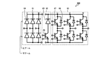
- FIG. 8 is a main part circuit diagram of the power semiconductor module 500. As shown in FIG. The circuit of the power semiconductor module 500 includes a converter unit 81, a brake unit 82, and an inverter unit 83.
- Converter portion 81 includes three phases of U phase, V phase and W phase, each phase is constituted by upper and lower arms, and each arm is constituted by diode 84.
- the brake unit 82 is composed of a diode 85 and an IGBT (insulated gate bipolar transistor) 86. In the brake unit 82, the diode 85 and the IGBT 86 are connected in series.
- the inverter unit 83 consists of three phases of U phase, V phase and W phase, and each phase is constituted by upper and lower arms.
- One arm in the inverter unit 83 includes an IGBT 87 and an FWD (Freewheeling diode) 88 which is a diode.
- the IGBTs 87 and the FWDs 88 are connected in antiparallel.
- the IGBTs 87 and the FWDs 88 may be connected alone or in parallel.
- the FWD 88 used in the inverter unit 83 has a reverse recovery mode, and destruction is likely to occur in this reverse recovery mode, so a high reverse recovery capability is required.
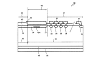
- FIG. 9 is a sectional view of an essential part of a conventional FWD 88. As shown in FIG. The sectional view of FIG. 9 is an enlarged view of the vicinity of the edge termination structure, and shows, for example, a structure similar to FIG.
- the FWD 88 is formed on the n anode region 54 and the anode end region 55 disposed on the n drift region 52 formed in the n semiconductor substrate 51, and on the n ⁇ region 53 which is an extension of the n drift region 52.
- P guard ring region 58 and p stopper region 59 arranged in FIG.
- the FWD 88 also includes an anode electrode 60 disposed on the p anode region 54 and on the anode end region 55.
- the FWD 88 further includes an insulating film 61 disposed on the p guard ring region 58 and the p stopper region 59. Further, the FWD 88 includes a guard ring electrode 62 electrically connected to the p guard ring region 58 and a stop electrode 63 electrically connected to the p stopper region 59.
- the impurity concentration and the diffusion depth of the anode end region 55 are the same as the impurity concentration and the diffusion depth of the p guard ring region 58.
- the FWD 88 also includes an n cathode region 65 disposed below the n drift region 52 and a cathode electrode 66 electrically connected to the n cathode region 65.
- the region where the p anode region 54 is formed is the active portion 64
- the region where the p guard ring region 58, the p stopper region 59, and the insulating film 61 are formed is the edge termination structure 67.
- reference numeral 52 denotes an n drift region
- reference numeral 53 denotes an n ⁇ region which is an extension of the n drift region 52.
- the IGBT 87 in the upper arm of the U phase and the IGBT 87 in the lower arm of the W phase are repeatedly turned on and off, increasing the on period increases the current flowing to the motor and increasing the off period decreases the current flowing to the motor.
- the number of revolutions and the torque of the motor are controlled by the increase and decrease of the current.
- the time when the FWD 88 transitions from the on state to the off state is referred to as a reverse recovery time, when the FWD 88 is on, when power is supplied.
- FIG. 10 is an explanatory view showing voltage-current waveforms of the IGBT 87 and the FWD 88.
- Section A is a state in which the IGBT 87 is turned on and current is supplied to the motor.
- Section B is a state in which the IGBT 87 is off. At this time, the current flowing to the motor loses a place to go, and flows through the inverter unit 83 through the FWD 88 of the other arm. This current is referred to as a return current and is a forward current for the FWD 88.
- Section C is a state in which the IGBT 87 is turned on again.
- the current flowing when the IGBT 87 is turned on is the current flowing to the motor and the reverse current of the FWD 88 connected in series to the IGBT 87.
- the reverse current flowing to the FWD 88 is stopped when the FWD 88 reverse recovers, and all the current flows to the motor.
- the series of operations are repeated to control the current flowing to the motor.
- the reverse current flowing to the FWD 88 is a reverse recovery current, and the time when the reverse recovery current is flowing is “reverse recovery time”.
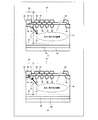
- FIG. 11 is a diagram for explaining the behavior of holes flowing in the FWD 88, wherein (a) is a diagram at the time of energization, and (b) is a diagram at the time of reverse recovery.
- the behavior of holes flowing to the FWD 88 in particular, the behavior from the active portion 64 to the edge termination structure 67 is shown.
- accumulation of the hole-electron pair also occurs in the n drift region 52 below the active portion 64 at the time of energization, the illustration is omitted.
- holes are injected from the p anode region 54 to the n ⁇ region 53 of the n drift region 52 and the extension part of the n drift region 52 (see reference numeral 71 in FIG. 11A). ). Electrons are injected from n cathode region 65 into n drift region 52 and n ⁇ region 53 so as to neutralize the holes. As a result, forward current flows in the n drift region 52 and the n ⁇ region 53 in the state in which the excess holes and the excess electrons are present (the accumulated state of the hole-electron pair).
- the state where the excess holes and electrons are present and the forward current flows is called conductivity modulation, and is a state in which the resistances of the n drift region 52 and the n ⁇ region 53 are significantly reduced. That is, when the current is supplied, excess holes and electrons are accumulated in the n drift region 52 and the n ⁇ region 53.
- the IGBT 87 is turned on again, and the FWD 88 shifts to a reverse recovery process in which a reverse recovery current flows.
- the FWD 88 shifts to a reverse recovery process in which a reverse recovery current flows.
- holes and electrons accumulated in n drift region 52 and n - region 53 are extracted from the holes (see reference numeral 73 in FIG. 11 (b)).
- electrons are drawn to the n cathode region 65 to become a reverse recovery current.
- the reverse recovery current disappears, and the FWD 88 is turned off.
- the pn junction between the anode end region 55 and the n drift region 52 has a convex shape in the depth direction. Therefore, current concentration is more likely to occur compared to the flat bottom of the p anode region 54.
- the holes accumulated in the n ⁇ region 53 under the edge termination structure 67 intensively flow in the anode end region 55 at the time of reverse recovery, thereby causing the destruction of the FWD 88.
- a method of forming a resistive region 56 between the p anode region 54 and the p guard ring region 58 which is the edge termination structure 67 (for example, See FIG. 1 of Patent Document 1). Also disclosed is a method of locally shortening the lifetime near the junction of the p anode region 54 and the edge termination structure 67 and the n drift region 52 and the n - region 53 of the extension thereof (eg, See FIG. 1 in reference 2).
- FIG. 12 is a cross-sectional view of an essential part of the FWD 88 having the extension structure 68.
- the difference between the FWD 88 shown in FIG. 12 and the FWD 88 shown in FIG. 9 is that the p anode region 54 is extended in the outer peripheral direction between the p anode region 54 and the p guard ring region 58 which is the edge termination structure 67.
- the point is that the resistance region 56 is provided.
- the anode electrode 60 is separated via an insulating film.
- FIG. 3 of Patent Document 3 described below describes an intermediate layer which is lower in concentration than the guard ring and shallower and higher in concentration than the anode low concentration layer. However, this middle layer is not connected to the guard ring. Also, the contact end and the low concentration layer are in contact.
- the action by resistance is described with the same structure as that of the conventional example.
- FIG. 1 of Patent Document 5 described below describes a configuration in which the contact end is covered with a p-ring which is deeper than the anode layer and suggested to have a low concentration.
- the selection of the resistance value Rpo of the resistance region 56 becomes important. If the resistance value Rpo is not set to the optimum value, current concentration easily occurs at the end of the edge termination structure 67 side or the active portion 64 side in the resistance region 56, and destruction of the FWD 88 occurs.
- FIG. 13 shows the behavior of holes in the case where the resistance value Rpo of the resistance region 56 is smaller than the optimum value in the FWD 88 of FIG. 12, (a) being a diagram during energization, (b) a diagram during reverse recovery. is there.
- hole injection (see reference numeral 71 in FIG. 13 (a)) is performed in a wide region at the time of energization.
- the power loss which is the product of the rated current and the forward voltage drop is sufficiently small, the element is not broken such as heat.
- FIG. 14 shows the behavior of holes in the case where the resistance value Rpo of the resistance region 56 is larger than the optimum value in the FWD 88 of FIG. 12, (a) being a diagram during energization, (b) a diagram during reverse recovery. is there.
- hole injection is performed in a wide region at the time of energization (see reference numeral 71 in FIG. 14 (a)).
- the resistance Rpo of the resistance region 56 is large, the hole injection amount decreases as going from the contact end 30 toward the outer periphery of the chip.
- the power loss which is the product of the rated current and the forward voltage drop is sufficiently small, so that no element breakage such as heat generation occurs.
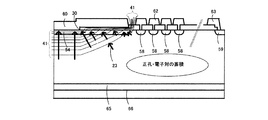
- FIG. 15 is a schematic diagram showing the relationship between equipotential lines and hole extraction (see reference numeral 73 in FIG. 14B) in reverse recovery in the diode of FIG. 14B.
- the equipotential line 41 is curved toward the active portion as shown in the figure, so that the gradient is concentrated toward the contact end 30.
- symbol 23 has shown extraction of the hole. Since the holes run down the space charge region along the gradient of the equipotential line 41 (potential), all the holes accumulated on the chip outer peripheral side from the contact end 30 are concentrated on the contact end 30. .
- a semiconductor device includes a first semiconductor region of a second conductivity type on a first main surface of a semiconductor substrate of a first conductivity type, and is disposed so as to surround the first semiconductor region. And a plurality of second semiconductor regions of a second conductivity type constituting an edge termination structure.
- a first main electrode electrically connected to the first semiconductor region is provided on the first main surface, and a depth from the first main electrode is provided between the second semiconductor region and the first semiconductor region.
- a third conductive region of a second conductivity type is provided which is a resistance region separated by an insulating film in a direction.
- two or more second semiconductor devices having different resistances in addition to the third semiconductor region may be provided on the surface of the semiconductor substrate in the direction of the outer periphery from the outer peripheral edge where the first main electrode contacts the semiconductor substrate.
- a conductive type diffusion region is provided, and any one of the third semiconductor region and the two or more second conductive type diffusion regions is connected to the first semiconductor region.
- the diffusion depth of at least one of the third semiconductor region and the two or more second conductivity type diffusion regions is larger than the diffusion depth of the remaining region.
- the depth may be deeper than the diffusion depth of the first semiconductor region.
- the first diffusion region of the two or more second conductivity type diffusion regions may be formed between the third semiconductor region and the first semiconductor region.
- the fifth semiconductor region of the second conductivity type is high and the diffusion depth is deep, and the diffusion depth of the fourth semiconductor region is deeper than the diffusion depth of the third semiconductor region, and the impurity concentration of the fourth semiconductor region is the The impurity concentration may be lower than the impurity concentration of the third semiconductor region.
- the width in the outer peripheral direction of the fifth semiconductor region is preferably 5 ⁇ m to 50 ⁇ m.
- the integral concentration of the third semiconductor region in the depth direction is higher than the impurity concentration of the first semiconductor region, and the two or more second conductivity type diffusion regions
- the first diffusion region is a fifth semiconductor region of the second conductivity type which is connected to the outer peripheral side of the third semiconductor region and has a diffusion depth deeper than that of the third semiconductor region and a high impurity concentration.
- the second diffusion region is a portion in which the first semiconductor region extends in the outer peripheral direction from the outer peripheral end of the first main electrode and the third semiconductor region You should connect to
- a length of the extension portion of the first semiconductor region is 2 ⁇ m or more and less than 50 ⁇ m.
- the third semiconductor region is a portion where the first semiconductor region extends in the outer peripheral direction from the outer peripheral end of the first main electrode, Among the above second conductivity type diffusion regions, the first diffusion region has a diffusion depth deeper than that of the third semiconductor region and a high impurity concentration and is connected to the outer peripheral side of the third semiconductor region A fifth semiconductor region, and a second diffusion region of the two or more second conductivity type diffusion regions is disposed to penetrate the third semiconductor region from the surface of the third semiconductor region in contact with the insulating film.
- the impurity concentration of the sixth semiconductor region is higher than the impurity concentration of the third semiconductor region.
- the impurity concentration and the diffusion depth of the third semiconductor region disposed between the sixth semiconductor region and the first semiconductor region are the same as those of the first semiconductor region. It is good to be equal to the impurity concentration and the diffusion depth.
- the impurity concentration and the diffusion depth of the third semiconductor region may be equal to the impurity concentration and the diffusion depth of the first semiconductor region.
- the reverse recovery current be shunted to the inner peripheral side than the outer peripheral end of the first main electrode by providing the second conductivity type diffusion region.
- a resistance region is provided between the p anode region and the p guard ring region constituting the edge termination structure, and a low concentration p diffusion region in contact with both is provided between the p anode region and the resistance region. Further, by providing a high concentration region in the surface layer of the p diffusion region, current concentration in the vicinity of the contact end of the anode electrode is suppressed.
- the resistance region which is deeper in diffusion depth than the p anode region and shallower than the diffusion depth of the p guard ring region is disposed in contact with the p anode region and the p guard ring region.
- the current concentration in the vicinity of the contact end of the anode electrode is suppressed by retracting the end of the portion in contact with the anode electrode toward the inside from the end of the p anode region and setting the amount of retraction to 2 ⁇ m to 50 ⁇ m.
- the present invention it is possible to avoid current concentration which is likely to occur at the boundary between the edge termination structure region and the active portion, and to provide a semiconductor device having a high reverse recovery capability.
- FIG. 1 is a cross-sectional view of an essential part of a semiconductor device 100 according to a first embodiment of the present invention.
- FIG. 2 is a diagram for explaining the behavior of holes in the structure of FIG. 1, (a) is a diagram at the time of energization, and (b) is a diagram at the time of reverse recovery.
- FIG. 3 is a cross-sectional view of main parts of a semiconductor device 200 according to a second embodiment of the present invention.
- FIG. 4 is a cross-sectional view of main parts of a semiconductor device 300 according to a third embodiment of the present invention.
- FIG. 5 is a diagram showing the relationship between the amount of retreat of the anode contact and the electric field strength.
- FIG. 6 is a cross-sectional view of main parts of a semiconductor device 400 according to a fourth embodiment of the present invention.
- FIG. 7 is a main part configuration diagram around the p anode region 4 of the semiconductor devices 100 to 400 of the first to fourth embodiments.
- FIG. 8 is a main part circuit diagram of the power semiconductor module 500.
- FIG. 9 is a sectional view of an essential part of a conventional FWD 88.
- FIG. 10 is an explanatory view showing voltage-current waveforms of the IGBT 87 and the FWD 88. As shown in FIG. FIG. FIG.
- FIG. 11 is a diagram for explaining the behavior of holes flowing in the FWD 88, wherein (a) is a diagram at the time of energization, and (b) is a diagram at the time of reverse recovery.
- FIG. 12 is a cross-sectional view of an essential part of the FWD 88 having the extension structure 68.
- FIG. 13 shows the behavior of holes in the case where the resistance value Rpo of the resistance region 56 is smaller than the optimum value in the FWD 88 of FIG. 12, (a) being a diagram during energization, (b) a diagram during reverse recovery. is there.
- FIG. 14 shows the behavior of holes in the case where the resistance value Rpo of the resistance region 56 is larger than the optimum value in the FWD 88 of FIG.
- FIG. 15 is a schematic diagram showing the relationship between equipotential lines and hole extraction (see reference numeral 73 in FIG. 14B) in reverse recovery in the diode of FIG. 14B.
- FIG. 16 is a schematic view showing the relationship between the equipotential line 41 and the extraction of holes (see reference numeral 23 in FIG. 16) in reverse recovery in the cross section of the diode of the first embodiment.
- FIG. 17 is a schematic view showing the relationship between the equipotential line 41 and the extraction of holes (see reference numeral 23 in FIG. 17) in reverse recovery in the cross section of the diode of the third embodiment.
- FIG. 18 is a schematic view showing the relationship between equipotential line 41 and hole extraction (see reference numeral 23 in FIG. 18) at the time of reverse recovery in the cross section of the diode of the fourth embodiment.
- Embodiments are described in the following examples.
- p at the beginning of the region indicates that the conductivity type is p-type
- n indicates that the conductivity type is n-type.
- chips a state in which a wafer to be a semiconductor substrate is fragmented into individual semiconductor devices.
- FIG. 1 is a cross-sectional view of an essential part of a semiconductor device 100 according to a first embodiment of the present invention.
- FIG. 1 is a cross-sectional view of a main part of the FWD corresponding to the FWD 88 of FIG. 8, and shows a cross-section of the main part of the semiconductor device from the vicinity of the end of the active part to the outer peripheral part of the semiconductor substrate.
- the semiconductor device 100 includes a p-anode region 4 disposed on the top surface of the n-drift region 2.
- p diffusion region 5 which is disposed in contact with p anode region 4 and which has a lower concentration and diffusion depth than p anode region 4 is provided.
- An edge termination structure 17 or the like is formed in the n ⁇ region 3 of the extension of the n drift region 2.
- Resistor region 6 arranged in contact with p diffusion region 5, resistance end region 7 arranged in contact with resistance region 6, and resistance end region 7 are separated on n ⁇ region 3.
- a plurality of p guard ring regions 8 and p stopper regions 9 spaced apart from the p guard ring regions 8 are provided.
- the regions formed in the n semiconductor substrate 1 are not formed in the n drift region 2 of the n semiconductor substrate 1 and the n ⁇ region 3 of the extended portion thereof.
- the semiconductor device 100 also includes an anode electrode 10 electrically connected to the p anode region 4 and the p diffusion region 5.
- anode electrode 10 electrically connected to the p anode region 4 and the p diffusion region 5.
- the portion of the end of the contact surface where the anode electrode 10 is connected to the surface of the p-anode region 4 or the p-type diffusion layer connected thereto is referred to as the contact end 30.
- a region from the contact end 30 toward the outer periphery of the chip from the outer peripheral end of the resistance end region 7 will be referred to as a buffer region 18.
- the semiconductor device 100 is characterized in that the buffer region 18 has three or more p-type regions different in electric resistance (hereinafter simply referred to as resistance).
- the semiconductor device 100 according to the first embodiment includes the p diffusion region 5 connected to the contact end 30, the resistance region 6 connected to the p-type diffusion region and the outer periphery side, and the resistance connected to the resistance region 6 and the outer periphery side It has three areas of the end area 7.
- the fact that these resistances are different specifically means that the integrated concentration obtained by integrating the impurity (doping) concentration of each of the three regions in the depth direction from the surface of the semiconductor substrate is different.
- the sheet resistance of each of the three regions is the reciprocal of the value obtained by multiplying the integral concentration by the carrier mobility (the hole in the case of the p-type layer) and the elementary charge, and thus the sheet resistance of each of the three regions is different. It is good.
- two may have the same resistance (integral density, sheet resistance).
- the buffer region 18 may have three p-type regions having at least two different resistance values.
- the semiconductor device 100 includes the insulating film 11 disposed on the n ⁇ region 3, the resistance region 6, the resistance end region 7, the p guard ring region 8, and the p stopper region 9.
- semiconductor device 100 is electrically connected on p guard ring region 8 to be disposed on insulating film 11 with guard ring electrode 12, and electrically connected on p stopper region 9 is disposed to be disposed.
- An electrode 13 is provided.
- the insulating film 11 may be a PSG (phosphorus glass) film, a thermal oxide film (including a field oxide film), or a laminated film of an oxide film and a PSG film.
- FIG. 1 shows a single insulating film, among them, for example, a composite film in which a thin thermal oxide film is only at a thin portion and a PSG film is deposited on a thermal oxide film at a thick portion. It may be
- the semiconductor device 100 includes an n cathode region 15 disposed under the n drift region 2 and the n ⁇ region 3 of the extension thereof, and a cathode electrode 16 disposed electrically connected to the n cathode region 15.
- a cathode electrode 16 disposed electrically connected to the n cathode region 15.
- the impurity concentration of the n drift region 2 and the n ⁇ region 3 of the extension portion is the same as the impurity concentration of the n semiconductor substrate 1 and is, for example, about 10 13 cm ⁇ 3 .
- the impurity concentration of the n drift region 2 and the n ⁇ region 3 of the extension portion may be different from the impurity concentration of the n semiconductor substrate 1.
- the p anode region 4 has an impurity concentration of, for example, about 2 ⁇ 10 16 cm ⁇ 3 (for example, 3 ⁇ 10 15 cm ⁇ 3 to 1 ⁇ 10 17 cm ⁇ 3 ) and a diffusion depth of, for example, about 5 ⁇ m (for example, 3 ⁇ m to 7 ⁇ m).
- the integral concentration in the p-anode region 4 is about 4 ⁇ 10 12 cm ⁇ 2 (eg, 4 ⁇ 10 11 cm ⁇ 2 to 3 ⁇ 10 13 cm ⁇ 2 ), assuming that the diffusion distribution is Gaussian.
- Sheet resistance is about 4000 ⁇ / ⁇ (1000 ⁇ / ⁇ to 30000 ⁇ / ⁇ ).
- the p guard ring region 8 is a p region (p + ) having a high impurity concentration.
- the p guard ring region 8 can have an impurity concentration of, for example, about 10 18 cm ⁇ 3 to 10 19 cm ⁇ 3 or more, and a diffusion depth of, for example, about 10 ⁇ m (eg, about 7 ⁇ m to 15 ⁇ m).
- the integrated concentration of the p guard ring region 8 is about 3 ⁇ 10 14 cm ⁇ 2 (for example, 2 ⁇ 10 14 cm ⁇ 2 to 4 ⁇ 10 15 cm ⁇ 2 ), and the sheet resistance is about 220 ⁇ / ⁇ (for example, 30 ⁇ ) / ⁇ to 300 ⁇ / ⁇ ).
- the resistive end region 7 is ap region having the same impurity concentration and diffusion depth as the p guard ring region 8. This resistive end region 7 can also be regarded as part of the p guard ring region 8.
- the resistance region 6 has an impurity concentration of about 10 17 cm -3 (for example, 3 ⁇ 10 16 cm -3 to 3 ⁇ 10 17 cm -3 ) and a diffusion depth of, for example, about 7 ⁇ m (for example, 5 ⁇ m to 10 ⁇ m) P region (p).
- the integrated concentration of the resistance region 6 is about 2.5 ⁇ 10 13 cm ⁇ 2 (for example, 5 ⁇ 10 12 cm ⁇ 2 to 1 ⁇ 10 14 cm ⁇ 2 ), and the sheet resistance is about 1100 ⁇ / ⁇ (for example, 400 ⁇ ) / ⁇ to 3000 ⁇ / ⁇ ).
- the p diffusion region 5 is a low concentration p region (p ⁇ ).
- the p diffusion region 5 has an impurity concentration of, for example, about 3 ⁇ 10 15 cm -3 (for example, 10 15 cm -3 to 10 16 cm -3 ), and a diffusion depth of about 10 ⁇ m (for example, 8 ⁇ m to 15 ⁇ m). can be - the concentration of the p region (p).
- the integrated concentration of the p diffusion region 5 is about 1.4 ⁇ 10 12 cm ⁇ 2 (for example, 4 ⁇ 10 11 cm ⁇ 2 to 6 ⁇ 10 12 cm ⁇ 2 ), and the sheet resistance is about 10000 ⁇ / ⁇ (for example, It is 2000 ⁇ / ⁇ to 30000 ⁇ / ⁇ ).
- the p diffusion region 5 has the function of suppressing the injection of holes into the n - region 3 to reduce the amount of accumulated holes, and the function of relaxing the current concentration in the p anode region 4 at the time of reverse recovery.
- the width W may be in the range of 5 ⁇ m to 50 ⁇ m. If it is less than 5 ⁇ m, the degree of planarization is too small and current concentration at this point becomes large. On the other hand, if it exceeds 50 ⁇ m, the area of the p anode region 4 becomes small, and the on voltage of the FWD is increased. In addition, preferably, the range of 10 ⁇ m to 30 ⁇ m is good.
- the portion up to the contact end 30 in the p anode region 4 and the p diffusion region 5 is defined as an active portion 14. Further, a region where the p guard ring region 8, the p stopper region 9, and the insulating film 11 are formed is referred to as an edge termination structure 17.
- n cathode On the back surface of the n semiconductor substrate 1, a high concentration n cathode having an impurity concentration of about 10 18 cm -3 and a diffusion depth of about 1 ⁇ m under the n drift region 2 and under the n - region 3 of the extension thereof. Region 15 is disposed, and cathode electrode 16 electrically connected to n cathode region 15 is disposed.
- the cathode electrode 16 is formed of, for example, a three-layer metal film of Ti / Ni / Au.
- the anode electrode 10, the guard ring electrode 12 and the stop electrode 13 are formed of, for example, an Al-Si film.
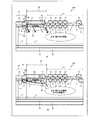
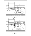
- FIG. 2 is a diagram for explaining the behavior of holes in the structure of FIG. 1, (a) is a diagram at the time of energization, and (b) is a diagram at the time of reverse recovery.
- FIG. 2 as in FIG. 11, accumulation of hole-electron pairs also occurs in the n drift region 2 below the active portion 14 when power is supplied, but illustration is omitted.
- FIG. 2A the injection 21 of holes from the p diffusion region 5 in contact with the resistance region 6 is smaller than that of the p anode region 4 at the time of energization. Also, the injection 21 of holes from the resistance region 6 decreases from the contact end 30 toward the edge termination structure 17 side.
- the injection 21 of holes from the resistance end region 7 provided on the innermost periphery of the edge termination structure 17 in contact with the outer end 6a of the resistance region 6 has a high impurity concentration in the resistance end region 7
- the injection 21 of holes from the inner end 6 b of the resistance region 6 is larger. Therefore, the location where the hole injection 21 becomes large is dispersed to the outer end 6 a and the inner end 6 b of the resistance region 6.
- the injection 21a of holes from the p diffusion region 5 is suppressed because the impurity concentration is low.
- the p diffusion region 5 itself functions as a current limiting resistor R because the impurity concentration is low. Therefore, the injection 21 a of holes from the p diffusion region 5 in contact with the resistance region 6 is suppressed as compared to the case where the p diffusion region 5 is not provided, and current concentration is suppressed.
- FIG. 2B at the time of reverse recovery, accumulation 22 of holes accumulated in the lower part of the edge termination structure 17 is extracted from the resistance end region 7 and the resistance region 6. Since the resistance value Rp is high in the resistance end region 7 and the resistance region 6, the holes are transferred to the p anode region 4 through the resistance region 6 (see the reference numeral 23 in FIG. 2B). A potential difference occurs when you This potential difference is approximately 100 to 200 V depending on the resistance of the resistance region 6.
- the amount of hole extraction (see reference numeral 23a in FIG. 2B) is small, and most of the accumulated hole accumulation 22 is extracted in the p diffusion region 5 and the p anode region 4. Also, the concentration of the p diffusion region 5 is lower than that of the p anode region 4 and the diffusion depth is deeper. Therefore, the accumulated holes 22 are not only directed to the contact end 30 but are also diverted to the p anode region 4 on the inner peripheral side of the p diffusion region 5, which causes current concentration to the contact end 30. In order to alleviate, reverse recovery tolerance is improved.
- FIG. 16 is a schematic view showing the relationship between the equipotential line 41 and the extraction of holes (see reference numeral 23 in FIG. 16) in reverse recovery in the cross section of the diode of the first embodiment.
- the equipotential lines 41 are illustrated only on the low voltage side, and the high voltage side (n cathode region 15 side) is not shown.
- the line at the same potential as the anode electrode 10 (which becomes the depletion layer end) in the p diffusion region 5 has a shallower distribution due to its lower concentration than the p anode region 4.
- the equipotential line 41 extends in the depth direction because the p diffusion region 5 is deep diffused. That is, equipotential lines 41 are distributed deeper than p anode region 4 and resistance region 6. Thereby, in the vicinity of the pn junction of this p diffusion region 5, the gradient of the potential becomes gentle. That is, the electric field strength is alleviated.
- the holes run down the space charge region along the potential gradient, so that the holes avoid this relaxation region and fall toward the steep side of the potential gradient, that is, the p anode region 4 side.
- the contact end 30 is located inside the low concentration p diffusion region 5. Therefore, holes are affected by the high resistance of the p diffusion region 5 and flow from the p anode region 4 having a lower resistance to the anode electrode 10. That is, the hole current is diverted to the p anode region 4 rather than the p diffusion region 5.
- the three p-type diffusion regions of the buffer region 18 may have at least two different diffusion depths in addition to the integral concentration as described above, and the effect of the diversion can be further enhanced.
- the holes flow from the p anode region 4 to the anode electrode 10 without being concentrated at the contact end 30, the current concentration at the contact end 30 is alleviated, and element breakdown is prevented. Further, as described above, by providing the p diffusion region 5, it is possible to prevent current concentration at the time of reverse recovery as well as at the time of energization. As a result, the semiconductor device 100 having high reverse recovery tolerance can be manufactured.
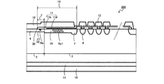
- FIG. 3 is a cross-sectional view of main parts of a semiconductor device 200 according to a second embodiment of the present invention.
- the difference from Example 1 is that a high concentration p region 25 (p + ) with a shallow diffusion depth is formed on the p anode region 4 and the p diffusion region 5.
- p + high concentration p region 25
- p diffusion region 5 When the surface concentration of the p diffusion region 5 is low, ohmic contact with the anode electrode 10 becomes difficult, and the contact resistance increases. As the contact resistance increases, the amount of holes extracted from the p diffusion region 5 decreases, and most of the holes are extracted in the p anode region 4. As a result, current concentration occurs in the p-anode region 4 to cause element breakdown.
- p region 25 which has a higher impurity concentration and a shallower diffusion depth than p diffusion region 5 in order to reduce the contact resistance with anode electrode 10 while keeping the impurity concentration in p diffusion region 5 low. It is good to provide.
- the amount of holes extracted in the p diffusion region 5 is increased, current concentration in the p anode region is improved, and element breakdown can be prevented.
- the impurity concentration in the p guard ring region 8 is high and the impurity concentration in the p diffusion region 5 is lowered in the first and second embodiments described above, the impurity concentration in the p guard ring region 8 is the impurity in the p diffusion region 5 It may be adjusted to the concentration. In this case, since both can be formed simultaneously, the manufacturing cost of the semiconductor devices 100 and 200 can be reduced.
- FIG. 4 is a cross-sectional view of main parts of a semiconductor device 300 according to a third embodiment of the present invention.
- the difference between this semiconductor device 300 and the first embodiment is the following two points.
- the first point is that the resistance region 26 which is deeper than the diffusion depth of the p anode region 4 and the resistance region 6 and shallower than the diffusion depth of the p guard ring region 8 is disposed in contact with the p anode region 4 and the resistance end region 7 is there.
- the second point is that the end of the portion where the p anode region 4 contacts the anode electrode 10 is separated (retracted) from the resistance region 26.
- the insulating film 11 is shown as a two-layer insulating film of PSG film 11b of phosphorus glass and thermal oxide film 11a.
- the buffer region 18 of Example 3 also has three different resistance regions.
- the first resistance region is a p anode region 4 which extends (or recedes) a distance T from the contact end 30 to the chip periphery.
- the second resistance region is a resistance region 26 connected to the extension of the p anode region 4.
- the third resistance area is a resistance end area 7 connected to the outer peripheral side of the resistance area 26.
- the resistance region 26 By making the resistance region 26 deeper than the diffusion depth of the p anode region 4, the amount of holes extracted in the resistance region 26 increases, and the extraction of holes including the p anode region 4 is equalized. Ru.
- the surface impurity concentration of the resistance region 26 is equal to the surface impurity concentration of the resistance region 6, the diffusion depth of the resistance region 26 is deeper than the diffusion depth of the resistance region 6.
- the value Rp1 is smaller than the resistance value Rp of the resistance region 6 (see FIG. 3).
- the integrated concentrations of p anode region 4 and resistance region 26 are different.
- the resistance end region 7 has the same high concentration as the p guard ring region 8 and a deep diffusion depth, so the resistance value is low.
- the effect of extracting holes is higher in the resistance region 26 than in the resistance region 6, and the extraction of holes including the p anode region 4 is equalized.
- the resistance region 26 may have the same diffusion depth as the resistance region 6 described above. However, in the case where the resistance region 26 has the same diffusion depth as the above-described resistance region 6, the resistance depth is made deeper than the diffusion depth of the p anode region 4.
- the outer peripheral portion of the p anode region 4 not in contact with the anode electrode 10 acts as a resistor Ra. That is, the receding portion 27 of the p anode region 4 receded from the resistance region 26 functions like the p diffusion region 5 of the first and second embodiments.
- FIG. 17 is a schematic view showing the relationship between the equipotential line 41 and the extraction of holes (see reference numeral 23 in FIG. 17) in reverse recovery in the cross section of the diode of the third embodiment.
- the equipotential lines 41 are illustrated only on the low voltage side, and the high voltage side (n cathode region 15 side) is not shown.
- the equipotential line 41 at the time of reverse recovery is pushed out toward the n drift region 2 in the resistance region 26 whose diffusion depth is deeper than that of the p anode region 4. That is, as in the first embodiment, in the vicinity of the boundary between the p anode region 4 and the resistance region 26, the distribution of the equipotential lines 41 becomes wider, and the potential gradient is relaxed. As a result, the hole extraction (see reference numeral 23 in FIG. 17) is diverted toward the p anode region 4 rather than the contact end 30. Furthermore, since the contact end 30 is recessed from the boundary between the p anode region 4 and the resistance region 26, current concentration on the contact end 30 is avoided.
- the holes flow from the p anode region 4 to the anode electrode without being concentrated at the contact end 30, and the current concentration at the contact end 30 is alleviated and element breakdown is prevented.
- the width (set as the retraction amount T) of the receding portion 27 is set to a proper value, current concentration in the p anode region 4 can be suppressed at the time of reverse recovery, and element breakdown can be prevented.
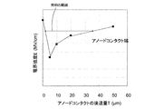
- FIG. 5 is a diagram showing the relationship between the amount of retreat of the anode contact and the electric field strength.
- E on the vertical axis is an arbitrary scale.
- the electric field strength E is the electric field strength at the time of reverse recovery.
- the electric field strength at which the element breaks is out of the range of the figure, but in order to ensure high reliability, it is necessary to be within the range of the illustrated invention. That is, it is preferable to set the retraction amount T in the range of 2 ⁇ m to 35 ⁇ m. If this range is exceeded, the electric field strength becomes high and high reliability can not be obtained. Further, a more preferable range is 3 ⁇ m to 10 ⁇ m.
- the three p-type diffusion regions of the buffer region 18 may have at least two different diffusion depths in addition to the integral concentration, and the effect of the diversion can be further enhanced.
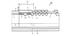
- FIG. 6 is a cross-sectional view of main parts of a semiconductor device 400 according to a fourth embodiment of the present invention.
- the difference between the first embodiment and the second embodiment is that the p diffusion region 5 is removed, and a high concentration p diffusion region 28 is disposed near the middle of the resistance region 6.
- the high concentration p diffusion region 28 is higher than the impurity concentration of the resistance region 6, and the diffusion depth is made deeper. Since the high concentration p diffusion region 28 efficiently withdraws the accumulated holes, current concentration is alleviated, and element breakdown can be prevented.
- the high concentration p diffusion region 28 can be disposed at any position within the resistance region 6.
- the resistance region 6 disposed between the p diffusion region 28 and the p anode region 4 may be formed simultaneously with the p anode region 4 to make the impurity concentration and the diffusion depth the same.
- the entire resistance region 6 may be formed simultaneously with the p anode region 4 to make the impurity concentration and the diffusion depth the same. In this case, since the manufacturing process is simplified, the manufacturing cost can be reduced.
- the buffer region 18 of Example 4 also has three different resistance regions.
- the first resistance region is a resistance region 6 in which the p anode region 4 extends from the contact end 30 to the chip outer peripheral side.
- the second resistance region is p diffusion region 28 connected to the extension of p anode region 4.
- the third resistance region is the same resistance region 6 as the first.
- the resistance value of the buffer region 18 is two kinds of the resistance region 6 having the same concentration distribution as the p anode region 4 and the p diffusion region 28.
- FIG. 18 is a schematic view showing the relationship between equipotential line 41 and hole extraction (see reference numeral 23 in FIG. 18) at the time of reverse recovery in the cross section of the diode of the fourth embodiment.
- the equipotential lines 41 are illustrated only on the low voltage side, and the high voltage side (n cathode region 15 side) is not shown.
- the equipotential line 41 at the time of reverse recovery is pushed out toward the n drift region 2 in the p diffusion region 28 whose diffusion depth is deeper than that of the p anode region 4 and the resistance region 6. That is, as in the first embodiment, the distribution of the equipotential lines 41 becomes wider near the boundary between the resistance region 6 and the p diffusion region 28, and the potential gradient is relaxed. As a result, the hole extraction 23 is diverted toward the p anode region 4 rather than the contact end 30. As a result, the holes flow from the p anode region 4 to the anode electrode 10 without being concentrated at the contact end 30, the current concentration at the contact end 30 is alleviated, and element breakdown is prevented.
- the effect of diversion can be increased.
- the three p-type diffusion regions of the buffer region 18 may have at least two different diffusion depths in addition to the integral concentration, and the effect of the diversion can be further enhanced.
- FIG. 7 is a main part configuration diagram around the p anode region 4 of the semiconductor devices 100 to 400 of the first to fourth embodiments. Here, eight examples are shown.
- the p ⁇ -anode region 31 having a low impurity concentration is disposed on the n drift region 2, and the anode electrode 10 is disposed thereon (the same figure (a)).
- a high concentration p region 32 with a shallow diffusion depth is disposed on the entire p ⁇ anode region 31 of (1), and the anode electrode 10 is disposed thereon.
- the p region 32 indicated by the thick line corresponds to the p region 25 shown in FIG. (The same figure (b)).
- the p region 32 of (2) is selectively disposed not on the entire region of the p ⁇ anode region 31 (FIG. 6 (c)).
- the high concentration p region 33 is selectively disposed in the p - anode region 31 of (1) ((d) in the figure).
- the p ⁇ -anode region 31 in (1) is replaced with a p-anode region 34 having a high impurity concentration and a shallow diffusion depth (the same figure (e)).
- a high concentration p region 32 with a shallow diffusion depth is disposed all over the p anode region 34 of (5), and the anode electrode 10 is disposed thereon (the same figure (f)).
- the p-anode region 34 of (5) is selectively disposed (FIG. 6 (g)).
- a high concentration p region 32 with a shallow diffusion depth is disposed in the whole area under the anode electrode 10 of (7) (FIG. 6 (h)).
- the semiconductor device according to the present invention is useful for a power semiconductor module.
Landscapes
- Electrodes Of Semiconductors (AREA)
Abstract
Description
(1)A区間は、IGBT87がオンしてモータに電流が供給された状態である。IGBT87がオンしてモータに電流が供給された状態ではFWD88には電流が流れていない。
(2)B区間は、IGBT87がオフした状態である。このとき、モータに流れる電流は行き場を失い、他のアームのFWD88を介して、インバータ部83を流れる。この電流は、還流電流といわれ、FWD88にとっては順方向電流となる。このFWD88に順方向電流が流れているときが「通電時」である。
(3)Cの区間は、IGBT87を再度オンさせた状態である。IGBT87のオンにより流れる電流は、モータに流れる電流とこのIGBT87に直列接続するFWD88の逆電流となる。FWD88に流れる逆電流は、FWD88が逆回復した段階で停止し、全ての電流はモータに流れる。この一連の動作を繰り返してモータに流れる電流は制御される。FWD88に流れる逆電流が逆回復電流であり、この逆回復電流が流れているときが「逆回復時」である。
(1)nドリフト領域2上に不純物濃度が低いp-アノード領域31を配置し、その上にアノード電極10を配置する(同図(a))。
(2)(1)のp-アノード領域31上全域に拡散深さの浅い高濃度のp領域32を配置し、その上にアノード電極10を配置する。この太線で示すp領域32は図3に示すp領域25に相当する。(同図(b))。
(3)(2)のp領域32をp-アノード領域31上の全域でなく選択的に配置する(同図(c))。
(4)(1)のp-アノード領域31内に高濃度のp領域33を選択的に配置する(同図(d))。
(5)(1)のp-アノード領域31を不純物濃度が高い、拡散深さが浅いpアノード領域34に置き換える(同図(e))。
(6)(5)のpアノード領域34上の全域に拡散深さの浅い高濃度のp領域32を配置し、その上にアノード電極10を配置する(同図(f))。
(7)(5)のpアノード領域34を選択的に配置する(同図(g))。
(8)(7)のアノード電極10下の全域に拡散深さの浅い高濃度のp領域32を配置する(同図(h))。
2 nドリフト領域
3 n-領域
4,54 pアノード領域
5,28 p拡散領域
5a 底部
6,26,56 抵抗領域
6a 外端部
6b 内端部
7 抵抗端部領域
8 pガードリング領域
9 pストッパ領域
10,60 アノード電極
11 絶縁膜
11a 熱酸化膜
11b PSG膜
12 ガードリング電極
13 ストップ電極
14,64 活性部
15 nカソード領域
16 カソード電極
17,67 エッジ終端構造
18 緩衝領域
21,21a,71 正孔の注入
22 正孔の蓄積
23,23a,73 正孔の引き抜き
25 p領域
27 後退箇所
30 コンタクト端
31 p-アノード領域
32,33 p領域
34 pアノード領域
41 等電位線
57 延長端部領域
68 延長構造
87 IGBT
88 FWD
100,200,300,400 半導体装置
W,T 幅
R,Ra 抵抗体
Rp,Rp1 抵抗値
Claims (11)
- 第1導電型の半導体基板と、
該半導体基板の第1主面に形成され、主たる電流を流す活性領域と、
該活性領域を取り囲んで配置されるエッジ終端構造と、
前記活性領域に形成された第2導電型の第1半導体領域と、
前記エッジ終端構造を構成する複数の第2導電型の第2半導体領域と、
前記第1主面上に形成され、前記第1半導体領域に電気的に接続する第1主電極と、
前記第2半導体領域と前記第1半導体領域の間に、前記第1主電極から深さ方向に絶縁膜を挟んで離間した抵抗領域となる第2導電型の第3半導体領域と、
前記第1主電極が前記半導体基板と接触する外周端部からさらに外周方向の前記半導体基板表面に形成され、前記第3半導体領域の他に抵抗の異なる2つ以上の第2導電型拡散領域と、を備えることを特徴とする半導体装置。 - 前記第3半導体領域および前記2つ以上の第2導電型拡散領域のいずれか1つが前記第1半導体領域に接続することを特徴とする請求項1に記載の半導体装置。
- 前記第3半導体領域および前記2つ以上の第2導電型拡散領域のうち少なくとも1つの領域の拡散深さが残余の領域の拡散深さよりも深く、かつ前記第1半導体領域の拡散深さよりも深いことを特徴とする請求項1または2に記載の半導体装置。
- 前記2つ以上の第2導電型拡散領域のうち第1の拡散領域が、前記第3半導体領域と前記第1半導体領域の間に両方に連接する第2導電型の第4半導体領域であり、
前記2つ以上の第2導電型拡散領域のうち第2の拡散領域が、前記第2半導体領域側で前記第3半導体領域より不純物濃度が高くかつ拡散深さが深い第2導電型の第5半導体領域であり、
前記第4半導体領域の拡散深さが前記第3半導体領域の拡散深さより深く、
前記第4半導体領域の不純物濃度が前記第3半導体領域の不純物濃度より低いことを特徴とする請求項1に記載の半導体装置。 - 前記第5半導体領域の外周方向の幅は5μm以上50μm以下であることを特徴とする請求項4に記載の半導体装置。
- 前記第3半導体領域の深さ方向の積分濃度が、前記第1半導体領域の不純物濃度より高く、
前記2つ以上の第2導電型拡散領域のうち第1の拡散領域が、前記第3半導体領域よりも拡散深さが深く不純物濃度が高いとともに該第3半導体領域の外周側に接続する第2導電型の第5半導体領域であり、
前記2つ以上の第2導電型拡散領域のうち第2の拡散領域が、前記第1半導体領域が前記第1主電極の外周端部から外周方向に延在した部分であるとともに前記第3半導体領域に接続することを特徴とする請求項1に記載の半導体装置。 - 前記第1半導体領域の延在部分の長さが2μm以上50μm未満であることを特徴とする請求項6に記載の半導体装置。
- 前記第3半導体領域は、前記第1半導体領域が前記第1主電極の外周端部から外周方向に延在した部分であり、
前記2つ以上の第2導電型拡散領域のうち第1の拡散領域が、前記第3半導体領域よりも拡散深さが深く不純物濃度が高いとともに該第3半導体領域の外周側に接続する第2導電型の第5半導体領域であり、
前記2つ以上の第2導電型拡散領域のうち第2の拡散領域が、前記絶縁膜に接する前記第3半導体領域の表面から前記第3半導体領域を貫通して配置される第2導電型の第6半導体領域であり、
該第6半導体領域の不純物濃度が前記第3半導体領域の不純物濃度より高いことを特徴とする請求項1に記載の半導体装置。 - 前記第6半導体領域と前記第1半導体領域の間に配置される前記第3半導体領域の不純物濃度と拡散深さが前記第1半導体領域の不純物濃度と拡散深さに等しいことを特徴とする請求項8に記載の半導体装置。
- 前記第3半導体領域の不純物濃度と拡散深さが前記第1半導体領域の不純物濃度と拡散深さに等しいことを特徴とする請求項8に記載の半導体装置。
- 前記第2導電型拡散領域を備えることにより、前記第1主電極の外周端部よりも内周側に逆回復電流を分流させることを特徴とする請求項1に記載の半導体装置。
Priority Applications (4)
| Application Number | Priority Date | Filing Date | Title |
|---|---|---|---|
| CN201480007250.6A CN104969359B (zh) | 2013-03-21 | 2014-03-14 | 半导体装置 |
| JP2015506750A JP6103038B2 (ja) | 2013-03-21 | 2014-03-14 | 半導体装置 |
| DE112014001529.6T DE112014001529T5 (de) | 2013-03-21 | 2014-03-14 | Halbleitervorrichtung |
| US14/821,348 US9450110B2 (en) | 2013-03-21 | 2015-08-07 | Semiconductor device |
Applications Claiming Priority (2)
| Application Number | Priority Date | Filing Date | Title |
|---|---|---|---|
| JP2013-058528 | 2013-03-21 | ||
| JP2013058528 | 2013-03-21 |
Related Child Applications (1)
| Application Number | Title | Priority Date | Filing Date |
|---|---|---|---|
| US14/821,348 Continuation US9450110B2 (en) | 2013-03-21 | 2015-08-07 | Semiconductor device |
Publications (1)
| Publication Number | Publication Date |
|---|---|
| WO2014148400A1 true WO2014148400A1 (ja) | 2014-09-25 |
Family
ID=51580083
Family Applications (1)
| Application Number | Title | Priority Date | Filing Date |
|---|---|---|---|
| PCT/JP2014/057012 Ceased WO2014148400A1 (ja) | 2013-03-21 | 2014-03-14 | 半導体装置 |
Country Status (5)
| Country | Link |
|---|---|
| US (1) | US9450110B2 (ja) |
| JP (1) | JP6103038B2 (ja) |
| CN (1) | CN104969359B (ja) |
| DE (1) | DE112014001529T5 (ja) |
| WO (1) | WO2014148400A1 (ja) |
Cited By (4)
| Publication number | Priority date | Publication date | Assignee | Title |
|---|---|---|---|---|
| JP2021027092A (ja) * | 2019-08-01 | 2021-02-22 | 三菱電機株式会社 | 半導体装置 |
| JP2022036203A (ja) * | 2017-03-16 | 2022-03-04 | ローム株式会社 | 半導体装置 |
| WO2025142265A1 (ja) * | 2023-12-27 | 2025-07-03 | ミネベアパワーデバイス株式会社 | 半導体装置および電力変換装置 |
| WO2025216180A1 (ja) * | 2024-04-10 | 2025-10-16 | ローム株式会社 | 半導体装置 |
Families Citing this family (4)
| Publication number | Priority date | Publication date | Assignee | Title |
|---|---|---|---|---|
| US20160020279A1 (en) * | 2014-07-18 | 2016-01-21 | International Rectifier Corporation | Edge Termination Using Guard Rings Between Recessed Field Oxide Regions |
| JP6597102B2 (ja) | 2015-09-16 | 2019-10-30 | 富士電機株式会社 | 半導体装置 |
| JP6804379B2 (ja) * | 2017-04-24 | 2020-12-23 | 三菱電機株式会社 | 半導体装置 |
| EP4179576A1 (en) | 2021-09-29 | 2023-05-17 | Dynex Semiconductor Limited | Semiconductor device |
Citations (14)
| Publication number | Priority date | Publication date | Assignee | Title |
|---|---|---|---|---|
| JPH06334188A (ja) * | 1993-05-18 | 1994-12-02 | Hitachi Ltd | 半導体装置 |
| JPH08316480A (ja) * | 1995-03-15 | 1996-11-29 | Toshiba Corp | 高耐圧半導体素子 |
| JP2000049360A (ja) * | 1998-07-29 | 2000-02-18 | Mitsubishi Electric Corp | 半導体装置 |
| JP2000114550A (ja) * | 1998-10-06 | 2000-04-21 | Hitachi Ltd | ダイオード及び電力変換装置 |
| JP2000150859A (ja) * | 1998-11-18 | 2000-05-30 | Meidensha Corp | ダイオード |
| JP2002270857A (ja) * | 2001-03-07 | 2002-09-20 | Toshiba Corp | 半導体装置および電力変換装置 |
| JP2003101039A (ja) * | 2001-07-17 | 2003-04-04 | Toshiba Corp | 高耐圧半導体装置 |
| JP2005093550A (ja) * | 2003-09-12 | 2005-04-07 | Toshiba Corp | 半導体装置 |
| JP2008263217A (ja) * | 2008-06-05 | 2008-10-30 | Fuji Electric Device Technology Co Ltd | 半導体装置 |
| JP2009164486A (ja) * | 2008-01-09 | 2009-07-23 | Toyota Motor Corp | 縦型ダイオードとその製造方法 |
| JP2012151143A (ja) * | 2011-01-14 | 2012-08-09 | Toyota Motor Corp | 半導体装置 |
| JP2012186318A (ja) * | 2011-03-05 | 2012-09-27 | Shindengen Electric Mfg Co Ltd | 高耐圧半導体装置 |
| JP2014038937A (ja) * | 2012-08-16 | 2014-02-27 | Mitsubishi Electric Corp | 半導体装置 |
| JP2014075384A (ja) * | 2012-10-02 | 2014-04-24 | Mitsubishi Electric Corp | 半導体装置 |
Family Cites Families (6)
| Publication number | Priority date | Publication date | Assignee | Title |
|---|---|---|---|---|
| US5969400A (en) | 1995-03-15 | 1999-10-19 | Kabushiki Kaisha Toshiba | High withstand voltage semiconductor device |
| JP3444081B2 (ja) | 1996-02-28 | 2003-09-08 | 株式会社日立製作所 | ダイオード及び電力変換装置 |
| JP2005340528A (ja) | 2004-05-27 | 2005-12-08 | Fuji Electric Device Technology Co Ltd | 半導体装置およびその製造方法 |
| JP5092610B2 (ja) | 2007-08-01 | 2012-12-05 | トヨタ自動車株式会社 | 半導体装置 |
| WO2011013379A1 (en) * | 2009-07-31 | 2011-02-03 | Fuji Electric Systems Co., Ltd. | Semiconductor apparatus |
| EP2725623B1 (en) * | 2011-09-08 | 2019-10-30 | Fuji Electric Co., Ltd. | Semiconductor device |
-
2014
- 2014-03-14 WO PCT/JP2014/057012 patent/WO2014148400A1/ja not_active Ceased
- 2014-03-14 CN CN201480007250.6A patent/CN104969359B/zh active Active
- 2014-03-14 DE DE112014001529.6T patent/DE112014001529T5/de active Pending
- 2014-03-14 JP JP2015506750A patent/JP6103038B2/ja active Active
-
2015
- 2015-08-07 US US14/821,348 patent/US9450110B2/en active Active
Patent Citations (14)
| Publication number | Priority date | Publication date | Assignee | Title |
|---|---|---|---|---|
| JPH06334188A (ja) * | 1993-05-18 | 1994-12-02 | Hitachi Ltd | 半導体装置 |
| JPH08316480A (ja) * | 1995-03-15 | 1996-11-29 | Toshiba Corp | 高耐圧半導体素子 |
| JP2000049360A (ja) * | 1998-07-29 | 2000-02-18 | Mitsubishi Electric Corp | 半導体装置 |
| JP2000114550A (ja) * | 1998-10-06 | 2000-04-21 | Hitachi Ltd | ダイオード及び電力変換装置 |
| JP2000150859A (ja) * | 1998-11-18 | 2000-05-30 | Meidensha Corp | ダイオード |
| JP2002270857A (ja) * | 2001-03-07 | 2002-09-20 | Toshiba Corp | 半導体装置および電力変換装置 |
| JP2003101039A (ja) * | 2001-07-17 | 2003-04-04 | Toshiba Corp | 高耐圧半導体装置 |
| JP2005093550A (ja) * | 2003-09-12 | 2005-04-07 | Toshiba Corp | 半導体装置 |
| JP2009164486A (ja) * | 2008-01-09 | 2009-07-23 | Toyota Motor Corp | 縦型ダイオードとその製造方法 |
| JP2008263217A (ja) * | 2008-06-05 | 2008-10-30 | Fuji Electric Device Technology Co Ltd | 半導体装置 |
| JP2012151143A (ja) * | 2011-01-14 | 2012-08-09 | Toyota Motor Corp | 半導体装置 |
| JP2012186318A (ja) * | 2011-03-05 | 2012-09-27 | Shindengen Electric Mfg Co Ltd | 高耐圧半導体装置 |
| JP2014038937A (ja) * | 2012-08-16 | 2014-02-27 | Mitsubishi Electric Corp | 半導体装置 |
| JP2014075384A (ja) * | 2012-10-02 | 2014-04-24 | Mitsubishi Electric Corp | 半導体装置 |
Cited By (6)
| Publication number | Priority date | Publication date | Assignee | Title |
|---|---|---|---|---|
| JP2022036203A (ja) * | 2017-03-16 | 2022-03-04 | ローム株式会社 | 半導体装置 |
| JP7260682B2 (ja) | 2017-03-16 | 2023-04-18 | ローム株式会社 | 半導体装置 |
| JP2021027092A (ja) * | 2019-08-01 | 2021-02-22 | 三菱電機株式会社 | 半導体装置 |
| JP7257912B2 (ja) | 2019-08-01 | 2023-04-14 | 三菱電機株式会社 | 半導体装置 |
| WO2025142265A1 (ja) * | 2023-12-27 | 2025-07-03 | ミネベアパワーデバイス株式会社 | 半導体装置および電力変換装置 |
| WO2025216180A1 (ja) * | 2024-04-10 | 2025-10-16 | ローム株式会社 | 半導体装置 |
Also Published As
| Publication number | Publication date |
|---|---|
| JPWO2014148400A1 (ja) | 2017-02-16 |
| US20150349144A1 (en) | 2015-12-03 |
| DE112014001529T5 (de) | 2015-12-24 |
| CN104969359B (zh) | 2017-10-17 |
| CN104969359A (zh) | 2015-10-07 |
| JP6103038B2 (ja) | 2017-03-29 |
| US9450110B2 (en) | 2016-09-20 |
Similar Documents
| Publication | Publication Date | Title |
|---|---|---|
| JP6103038B2 (ja) | 半導体装置 | |
| JP6277814B2 (ja) | 半導体装置 | |
| JP6119577B2 (ja) | 半導体装置 | |
| US9799648B2 (en) | Semiconductor device | |
| JP5636808B2 (ja) | 半導体装置 | |
| JP6319057B2 (ja) | 逆導通型半導体装置 | |
| JP6424524B2 (ja) | 半導体装置および半導体装置の製造方法 | |
| JP6029411B2 (ja) | 半導体装置 | |
| JP2017059711A (ja) | 半導体装置 | |
| JP2013115223A (ja) | 半導体装置 | |
| CN105378932A (zh) | 半导体装置 | |
| JP6673439B2 (ja) | 半導体装置 | |
| JP5135719B2 (ja) | トレンチ型絶縁ゲート半導体装置 | |
| JP6946922B2 (ja) | 半導体装置 | |
| JP6804379B2 (ja) | 半導体装置 | |
| JP6101440B2 (ja) | ダイオードおよびそれを用いた電力変換装置 | |
| US11374091B2 (en) | Semiconductor device | |
| JP7171527B2 (ja) | 半導体装置および電力変換装置 | |
| JP6598756B2 (ja) | 電力用半導体装置およびその製造方法 | |
| JP6550995B2 (ja) | 半導体装置 | |
| JP6002387B2 (ja) | ダイオードおよびそれを用いた電力変換システム | |
| JP6048003B2 (ja) | Igbtとダイオードが同一半導体基板に形成されている半導体装置 | |
| JP6561496B2 (ja) | 半導体装置 |
Legal Events
| Date | Code | Title | Description |
|---|---|---|---|
| 121 | Ep: the epo has been informed by wipo that ep was designated in this application |
Ref document number: 14769999 Country of ref document: EP Kind code of ref document: A1 |
|
| ENP | Entry into the national phase |
Ref document number: 2015506750 Country of ref document: JP Kind code of ref document: A |
|
| WWE | Wipo information: entry into national phase |
Ref document number: 112014001529 Country of ref document: DE Ref document number: 1120140015296 Country of ref document: DE |
|
| 122 | Ep: pct application non-entry in european phase |
Ref document number: 14769999 Country of ref document: EP Kind code of ref document: A1 |