WO2014148392A1 - Dispositif photovoltaïque - Google Patents
Dispositif photovoltaïque Download PDFInfo
- Publication number
- WO2014148392A1 WO2014148392A1 PCT/JP2014/056939 JP2014056939W WO2014148392A1 WO 2014148392 A1 WO2014148392 A1 WO 2014148392A1 JP 2014056939 W JP2014056939 W JP 2014056939W WO 2014148392 A1 WO2014148392 A1 WO 2014148392A1
- Authority
- WO
- WIPO (PCT)
- Prior art keywords
- thin film
- amorphous silicon
- silicon thin
- photovoltaic device
- current collecting
- Prior art date
Links
- 239000010409 thin film Substances 0.000 claims abstract description 168
- 229910021417 amorphous silicon Inorganic materials 0.000 claims abstract description 157
- 239000010408 film Substances 0.000 claims abstract description 122
- 239000000758 substrate Substances 0.000 claims abstract description 79
- 239000004065 semiconductor Substances 0.000 claims abstract description 54
- 239000013078 crystal Substances 0.000 claims description 52
- 238000000034 method Methods 0.000 claims description 42
- 229910052751 metal Inorganic materials 0.000 claims description 30
- 239000002184 metal Substances 0.000 claims description 30
- 238000007733 ion plating Methods 0.000 claims description 13
- 229910021426 porous silicon Inorganic materials 0.000 claims description 2
- 238000010248 power generation Methods 0.000 description 20
- 230000000052 comparative effect Effects 0.000 description 15
- 229910021421 monocrystalline silicon Inorganic materials 0.000 description 11
- 238000005259 measurement Methods 0.000 description 10
- XUIMIQQOPSSXEZ-UHFFFAOYSA-N Silicon Chemical compound [Si] XUIMIQQOPSSXEZ-UHFFFAOYSA-N 0.000 description 9
- 238000005229 chemical vapour deposition Methods 0.000 description 9
- 238000005268 plasma chemical vapour deposition Methods 0.000 description 9
- 229910052710 silicon Inorganic materials 0.000 description 9
- 239000010703 silicon Substances 0.000 description 9
- 239000000463 material Substances 0.000 description 8
- 230000015572 biosynthetic process Effects 0.000 description 7
- 239000004020 conductor Substances 0.000 description 7
- 239000007789 gas Substances 0.000 description 7
- 238000012545 processing Methods 0.000 description 7
- KWYUFKZDYYNOTN-UHFFFAOYSA-M Potassium hydroxide Chemical compound [OH-].[K+] KWYUFKZDYYNOTN-UHFFFAOYSA-M 0.000 description 6
- HEMHJVSKTPXQMS-UHFFFAOYSA-M Sodium hydroxide Chemical compound [OH-].[Na+] HEMHJVSKTPXQMS-UHFFFAOYSA-M 0.000 description 6
- 238000004519 manufacturing process Methods 0.000 description 6
- 239000000853 adhesive Substances 0.000 description 5
- 230000001070 adhesive effect Effects 0.000 description 5
- 238000007639 printing Methods 0.000 description 5
- 230000006798 recombination Effects 0.000 description 5
- 238000005215 recombination Methods 0.000 description 5
- 238000004544 sputter deposition Methods 0.000 description 5
- 238000001771 vacuum deposition Methods 0.000 description 5
- 229910021419 crystalline silicon Inorganic materials 0.000 description 4
- 230000007423 decrease Effects 0.000 description 4
- 230000007547 defect Effects 0.000 description 4
- 230000000694 effects Effects 0.000 description 4
- 238000011156 evaluation Methods 0.000 description 4
- 239000012535 impurity Substances 0.000 description 4
- 229910052709 silver Inorganic materials 0.000 description 4
- 241001422033 Thestylus Species 0.000 description 3
- 238000000137 annealing Methods 0.000 description 3
- 238000006243 chemical reaction Methods 0.000 description 3
- 230000006866 deterioration Effects 0.000 description 3
- 230000001747 exhibiting effect Effects 0.000 description 3
- 239000011521 glass Substances 0.000 description 3
- 150000002739 metals Chemical class 0.000 description 3
- RYGMFSIKBFXOCR-UHFFFAOYSA-N Copper Chemical compound [Cu] RYGMFSIKBFXOCR-UHFFFAOYSA-N 0.000 description 2
- BQCADISMDOOEFD-UHFFFAOYSA-N Silver Chemical compound [Ag] BQCADISMDOOEFD-UHFFFAOYSA-N 0.000 description 2
- 229910045601 alloy Inorganic materials 0.000 description 2
- 239000000956 alloy Substances 0.000 description 2
- 229910052782 aluminium Inorganic materials 0.000 description 2
- QVGXLLKOCUKJST-UHFFFAOYSA-N atomic oxygen Chemical compound [O] QVGXLLKOCUKJST-UHFFFAOYSA-N 0.000 description 2
- 230000015556 catabolic process Effects 0.000 description 2
- 229910052804 chromium Inorganic materials 0.000 description 2
- 229910052802 copper Inorganic materials 0.000 description 2
- 239000010949 copper Substances 0.000 description 2
- 238000006731 degradation reaction Methods 0.000 description 2
- 239000007772 electrode material Substances 0.000 description 2
- 229910003437 indium oxide Inorganic materials 0.000 description 2
- PJXISJQVUVHSOJ-UHFFFAOYSA-N indium(iii) oxide Chemical compound [O-2].[O-2].[O-2].[In+3].[In+3] PJXISJQVUVHSOJ-UHFFFAOYSA-N 0.000 description 2
- AMGQUBHHOARCQH-UHFFFAOYSA-N indium;oxotin Chemical compound [In].[Sn]=O AMGQUBHHOARCQH-UHFFFAOYSA-N 0.000 description 2
- 150000002500 ions Chemical class 0.000 description 2
- 239000007769 metal material Substances 0.000 description 2
- 229910052759 nickel Inorganic materials 0.000 description 2
- 239000001301 oxygen Substances 0.000 description 2
- 229910052760 oxygen Inorganic materials 0.000 description 2
- 238000007747 plating Methods 0.000 description 2
- 239000004332 silver Substances 0.000 description 2
- 238000012360 testing method Methods 0.000 description 2
- XLOMVQKBTHCTTD-UHFFFAOYSA-N zinc oxide Inorganic materials [Zn]=O XLOMVQKBTHCTTD-UHFFFAOYSA-N 0.000 description 2
- 239000011787 zinc oxide Substances 0.000 description 2
- 229910052684 Cerium Inorganic materials 0.000 description 1
- 229910000577 Silicon-germanium Inorganic materials 0.000 description 1
- 238000010521 absorption reaction Methods 0.000 description 1
- 238000005452 bending Methods 0.000 description 1
- 230000005540 biological transmission Effects 0.000 description 1
- 239000000969 carrier Substances 0.000 description 1
- GWXLDORMOJMVQZ-UHFFFAOYSA-N cerium Chemical compound [Ce] GWXLDORMOJMVQZ-UHFFFAOYSA-N 0.000 description 1
- 229910000420 cerium oxide Inorganic materials 0.000 description 1
- 239000011651 chromium Substances 0.000 description 1
- 238000005520 cutting process Methods 0.000 description 1
- 230000003247 decreasing effect Effects 0.000 description 1
- 238000000151 deposition Methods 0.000 description 1
- 238000010586 diagram Methods 0.000 description 1
- 239000002019 doping agent Substances 0.000 description 1
- 238000005530 etching Methods 0.000 description 1
- 239000005431 greenhouse gas Substances 0.000 description 1
- 238000009499 grossing Methods 0.000 description 1
- 238000010438 heat treatment Methods 0.000 description 1
- 229910052738 indium Inorganic materials 0.000 description 1
- APFVFJFRJDLVQX-UHFFFAOYSA-N indium atom Chemical compound [In] APFVFJFRJDLVQX-UHFFFAOYSA-N 0.000 description 1
- ATFCOADKYSRZES-UHFFFAOYSA-N indium;oxotungsten Chemical compound [In].[W]=O ATFCOADKYSRZES-UHFFFAOYSA-N 0.000 description 1
- 238000010030 laminating Methods 0.000 description 1
- 230000031700 light absorption Effects 0.000 description 1
- 238000000691 measurement method Methods 0.000 description 1
- 230000008018 melting Effects 0.000 description 1
- 238000002844 melting Methods 0.000 description 1
- 239000012528 membrane Substances 0.000 description 1
- PXHVJJICTQNCMI-UHFFFAOYSA-N nickel Substances [Ni] PXHVJJICTQNCMI-UHFFFAOYSA-N 0.000 description 1
- 238000007645 offset printing Methods 0.000 description 1
- BMMGVYCKOGBVEV-UHFFFAOYSA-N oxo(oxoceriooxy)cerium Chemical compound [Ce]=O.O=[Ce]=O BMMGVYCKOGBVEV-UHFFFAOYSA-N 0.000 description 1
- 239000002245 particle Substances 0.000 description 1
- 238000005240 physical vapour deposition Methods 0.000 description 1
- 239000002994 raw material Substances 0.000 description 1
- 238000002310 reflectometry Methods 0.000 description 1
- 238000007650 screen-printing Methods 0.000 description 1
- 229910000679 solder Inorganic materials 0.000 description 1
- 230000003595 spectral effect Effects 0.000 description 1
- WFKWXMTUELFFGS-UHFFFAOYSA-N tungsten Chemical compound [W] WFKWXMTUELFFGS-UHFFFAOYSA-N 0.000 description 1
- 229910052721 tungsten Inorganic materials 0.000 description 1
- 239000010937 tungsten Substances 0.000 description 1
- 238000001039 wet etching Methods 0.000 description 1
- YVTHLONGBIQYBO-UHFFFAOYSA-N zinc indium(3+) oxygen(2-) Chemical compound [O--].[Zn++].[In+3] YVTHLONGBIQYBO-UHFFFAOYSA-N 0.000 description 1
Images

Classifications
-
- H—ELECTRICITY
- H01—ELECTRIC ELEMENTS
- H01L—SEMICONDUCTOR DEVICES NOT COVERED BY CLASS H10
- H01L31/00—Semiconductor devices sensitive to infrared radiation, light, electromagnetic radiation of shorter wavelength or corpuscular radiation and specially adapted either for the conversion of the energy of such radiation into electrical energy or for the control of electrical energy by such radiation; Processes or apparatus specially adapted for the manufacture or treatment thereof or of parts thereof; Details thereof
- H01L31/0248—Semiconductor devices sensitive to infrared radiation, light, electromagnetic radiation of shorter wavelength or corpuscular radiation and specially adapted either for the conversion of the energy of such radiation into electrical energy or for the control of electrical energy by such radiation; Processes or apparatus specially adapted for the manufacture or treatment thereof or of parts thereof; Details thereof characterised by their semiconductor bodies
- H01L31/036—Semiconductor devices sensitive to infrared radiation, light, electromagnetic radiation of shorter wavelength or corpuscular radiation and specially adapted either for the conversion of the energy of such radiation into electrical energy or for the control of electrical energy by such radiation; Processes or apparatus specially adapted for the manufacture or treatment thereof or of parts thereof; Details thereof characterised by their semiconductor bodies characterised by their crystalline structure or particular orientation of the crystalline planes
- H01L31/0376—Semiconductor devices sensitive to infrared radiation, light, electromagnetic radiation of shorter wavelength or corpuscular radiation and specially adapted either for the conversion of the energy of such radiation into electrical energy or for the control of electrical energy by such radiation; Processes or apparatus specially adapted for the manufacture or treatment thereof or of parts thereof; Details thereof characterised by their semiconductor bodies characterised by their crystalline structure or particular orientation of the crystalline planes including amorphous semiconductors
- H01L31/03762—Semiconductor devices sensitive to infrared radiation, light, electromagnetic radiation of shorter wavelength or corpuscular radiation and specially adapted either for the conversion of the energy of such radiation into electrical energy or for the control of electrical energy by such radiation; Processes or apparatus specially adapted for the manufacture or treatment thereof or of parts thereof; Details thereof characterised by their semiconductor bodies characterised by their crystalline structure or particular orientation of the crystalline planes including amorphous semiconductors including only elements of Group IV of the Periodic System
-
- H—ELECTRICITY
- H01—ELECTRIC ELEMENTS
- H01L—SEMICONDUCTOR DEVICES NOT COVERED BY CLASS H10
- H01L31/00—Semiconductor devices sensitive to infrared radiation, light, electromagnetic radiation of shorter wavelength or corpuscular radiation and specially adapted either for the conversion of the energy of such radiation into electrical energy or for the control of electrical energy by such radiation; Processes or apparatus specially adapted for the manufacture or treatment thereof or of parts thereof; Details thereof
- H01L31/02—Details
- H01L31/02002—Arrangements for conducting electric current to or from the device in operations
- H01L31/02005—Arrangements for conducting electric current to or from the device in operations for device characterised by at least one potential jump barrier or surface barrier
- H01L31/02008—Arrangements for conducting electric current to or from the device in operations for device characterised by at least one potential jump barrier or surface barrier for solar cells or solar cell modules
- H01L31/0201—Arrangements for conducting electric current to or from the device in operations for device characterised by at least one potential jump barrier or surface barrier for solar cells or solar cell modules comprising specially adapted module bus-bar structures
-
- H—ELECTRICITY
- H01—ELECTRIC ELEMENTS
- H01L—SEMICONDUCTOR DEVICES NOT COVERED BY CLASS H10
- H01L31/00—Semiconductor devices sensitive to infrared radiation, light, electromagnetic radiation of shorter wavelength or corpuscular radiation and specially adapted either for the conversion of the energy of such radiation into electrical energy or for the control of electrical energy by such radiation; Processes or apparatus specially adapted for the manufacture or treatment thereof or of parts thereof; Details thereof
- H01L31/02—Details
- H01L31/0224—Electrodes
- H01L31/022408—Electrodes for devices characterised by at least one potential jump barrier or surface barrier
- H01L31/022425—Electrodes for devices characterised by at least one potential jump barrier or surface barrier for solar cells
- H01L31/022433—Particular geometry of the grid contacts
-
- H—ELECTRICITY
- H01—ELECTRIC ELEMENTS
- H01L—SEMICONDUCTOR DEVICES NOT COVERED BY CLASS H10
- H01L31/00—Semiconductor devices sensitive to infrared radiation, light, electromagnetic radiation of shorter wavelength or corpuscular radiation and specially adapted either for the conversion of the energy of such radiation into electrical energy or for the control of electrical energy by such radiation; Processes or apparatus specially adapted for the manufacture or treatment thereof or of parts thereof; Details thereof
- H01L31/02—Details
- H01L31/0224—Electrodes
- H01L31/022466—Electrodes made of transparent conductive layers, e.g. TCO, ITO layers
-
- H—ELECTRICITY
- H01—ELECTRIC ELEMENTS
- H01L—SEMICONDUCTOR DEVICES NOT COVERED BY CLASS H10
- H01L31/00—Semiconductor devices sensitive to infrared radiation, light, electromagnetic radiation of shorter wavelength or corpuscular radiation and specially adapted either for the conversion of the energy of such radiation into electrical energy or for the control of electrical energy by such radiation; Processes or apparatus specially adapted for the manufacture or treatment thereof or of parts thereof; Details thereof
- H01L31/0248—Semiconductor devices sensitive to infrared radiation, light, electromagnetic radiation of shorter wavelength or corpuscular radiation and specially adapted either for the conversion of the energy of such radiation into electrical energy or for the control of electrical energy by such radiation; Processes or apparatus specially adapted for the manufacture or treatment thereof or of parts thereof; Details thereof characterised by their semiconductor bodies
- H01L31/0256—Semiconductor devices sensitive to infrared radiation, light, electromagnetic radiation of shorter wavelength or corpuscular radiation and specially adapted either for the conversion of the energy of such radiation into electrical energy or for the control of electrical energy by such radiation; Processes or apparatus specially adapted for the manufacture or treatment thereof or of parts thereof; Details thereof characterised by their semiconductor bodies characterised by the material
- H01L31/0264—Inorganic materials
- H01L31/028—Inorganic materials including, apart from doping material or other impurities, only elements of Group IV of the Periodic System
-
- H—ELECTRICITY
- H01—ELECTRIC ELEMENTS
- H01L—SEMICONDUCTOR DEVICES NOT COVERED BY CLASS H10
- H01L31/00—Semiconductor devices sensitive to infrared radiation, light, electromagnetic radiation of shorter wavelength or corpuscular radiation and specially adapted either for the conversion of the energy of such radiation into electrical energy or for the control of electrical energy by such radiation; Processes or apparatus specially adapted for the manufacture or treatment thereof or of parts thereof; Details thereof
- H01L31/04—Semiconductor devices sensitive to infrared radiation, light, electromagnetic radiation of shorter wavelength or corpuscular radiation and specially adapted either for the conversion of the energy of such radiation into electrical energy or for the control of electrical energy by such radiation; Processes or apparatus specially adapted for the manufacture or treatment thereof or of parts thereof; Details thereof adapted as photovoltaic [PV] conversion devices
- H01L31/06—Semiconductor devices sensitive to infrared radiation, light, electromagnetic radiation of shorter wavelength or corpuscular radiation and specially adapted either for the conversion of the energy of such radiation into electrical energy or for the control of electrical energy by such radiation; Processes or apparatus specially adapted for the manufacture or treatment thereof or of parts thereof; Details thereof adapted as photovoltaic [PV] conversion devices characterised by at least one potential-jump barrier or surface barrier
- H01L31/072—Semiconductor devices sensitive to infrared radiation, light, electromagnetic radiation of shorter wavelength or corpuscular radiation and specially adapted either for the conversion of the energy of such radiation into electrical energy or for the control of electrical energy by such radiation; Processes or apparatus specially adapted for the manufacture or treatment thereof or of parts thereof; Details thereof adapted as photovoltaic [PV] conversion devices characterised by at least one potential-jump barrier or surface barrier the potential barriers being only of the PN heterojunction type
- H01L31/0745—Semiconductor devices sensitive to infrared radiation, light, electromagnetic radiation of shorter wavelength or corpuscular radiation and specially adapted either for the conversion of the energy of such radiation into electrical energy or for the control of electrical energy by such radiation; Processes or apparatus specially adapted for the manufacture or treatment thereof or of parts thereof; Details thereof adapted as photovoltaic [PV] conversion devices characterised by at least one potential-jump barrier or surface barrier the potential barriers being only of the PN heterojunction type comprising a AIVBIV heterojunction, e.g. Si/Ge, SiGe/Si or Si/SiC solar cells
- H01L31/0747—Semiconductor devices sensitive to infrared radiation, light, electromagnetic radiation of shorter wavelength or corpuscular radiation and specially adapted either for the conversion of the energy of such radiation into electrical energy or for the control of electrical energy by such radiation; Processes or apparatus specially adapted for the manufacture or treatment thereof or of parts thereof; Details thereof adapted as photovoltaic [PV] conversion devices characterised by at least one potential-jump barrier or surface barrier the potential barriers being only of the PN heterojunction type comprising a AIVBIV heterojunction, e.g. Si/Ge, SiGe/Si or Si/SiC solar cells comprising a heterojunction of crystalline and amorphous materials, e.g. heterojunction with intrinsic thin layer or HIT® solar cells; solar cells
-
- Y—GENERAL TAGGING OF NEW TECHNOLOGICAL DEVELOPMENTS; GENERAL TAGGING OF CROSS-SECTIONAL TECHNOLOGIES SPANNING OVER SEVERAL SECTIONS OF THE IPC; TECHNICAL SUBJECTS COVERED BY FORMER USPC CROSS-REFERENCE ART COLLECTIONS [XRACs] AND DIGESTS
- Y02—TECHNOLOGIES OR APPLICATIONS FOR MITIGATION OR ADAPTATION AGAINST CLIMATE CHANGE
- Y02E—REDUCTION OF GREENHOUSE GAS [GHG] EMISSIONS, RELATED TO ENERGY GENERATION, TRANSMISSION OR DISTRIBUTION
- Y02E10/00—Energy generation through renewable energy sources
- Y02E10/50—Photovoltaic [PV] energy
- Y02E10/547—Monocrystalline silicon PV cells
-
- Y—GENERAL TAGGING OF NEW TECHNOLOGICAL DEVELOPMENTS; GENERAL TAGGING OF CROSS-SECTIONAL TECHNOLOGIES SPANNING OVER SEVERAL SECTIONS OF THE IPC; TECHNICAL SUBJECTS COVERED BY FORMER USPC CROSS-REFERENCE ART COLLECTIONS [XRACs] AND DIGESTS
- Y02—TECHNOLOGIES OR APPLICATIONS FOR MITIGATION OR ADAPTATION AGAINST CLIMATE CHANGE
- Y02E—REDUCTION OF GREENHOUSE GAS [GHG] EMISSIONS, RELATED TO ENERGY GENERATION, TRANSMISSION OR DISTRIBUTION
- Y02E10/00—Energy generation through renewable energy sources
- Y02E10/50—Photovoltaic [PV] energy
- Y02E10/548—Amorphous silicon PV cells
Definitions
- the present invention relates to a photovoltaic device, and more particularly to a photovoltaic device (solar cell) having a heterojunction.
- Photovoltaic power generation devices are attracting attention as clean power generation means that does not generate greenhouse gases such as CO 2 and as power generation means with high operational safety that can replace nuclear power generation.
- One of the photovoltaic devices is a photovoltaic device having a heterojunction with high power generation efficiency.
- this photovoltaic device 60 having a heterojunction is provided on both sides of a photovoltaic element 61 that generates power by light irradiation, and on the photovoltaic element 61.
- Current collecting members 62 and 63 for collecting the generated electric power.
- a first intrinsic amorphous silicon thin film 65, a p-type amorphous silicon thin film 66, and a first transparent conductive film 67 are laminated in this order on one side of an n-type crystal semiconductor substrate 64.
- the first intrinsic amorphous silicon thin film 65 between the n-type crystal semiconductor substrate 64 and the p-type amorphous silicon thin film 66 the n-type crystal semiconductor substrate 64 and the p-type non-crystalline silicon thin film 65 are provided.
- the current collecting member 62 (63) includes a plurality of bus bar electrodes 71 formed in parallel to each other and a plurality of finger electrodes 72 connected to the bus bar electrodes 71 and formed in parallel to each other. By making the current collecting member 62 (63) in such a shape, efficient current collection is performed while suppressing light shielding by the current collecting member itself.
- the thickness of the p-type amorphous silicon thin film 66 is large, specifically, for example, preferably 6 nm or more (see Patent Document 1). .
- the first transparent conductive film 67 laminated on the p-type amorphous silicon thin film 66 is usually formed by sputtering. Therefore, it is said that by using the p-type amorphous silicon thin film 66 having a certain film thickness, it is possible to prevent surface degradation due to sputtering and to suppress the performance degradation of the photovoltaic power generation device 60.
- further improvement is required to increase the fill factor.
- the present invention has been made in view of such circumstances, and an object thereof is to provide a photovoltaic device having a high fill factor (curve factor).
- the present inventor has (1) increasing the film thickness of the p-type amorphous silicon thin film to increase the series resistance and conversely decreasing the fill factor. (2) In order to increase the fill factor, p. It is effective to reduce the thickness of the p-type amorphous silicon thin film and to reduce the distance between the finger electrodes provided on the p-type amorphous silicon thin film side, and (3) It has been found that even if the distance between the finger electrodes provided on the n-type amorphous silicon thin film side is reduced, the fill factor is not improved, and the present invention has been achieved based on these findings.
- the photovoltaic device that meets the above-mentioned purpose is A multilayer photovoltaic device, a first current collecting member laminated on one surface of the photovoltaic device, and a second current collecting member laminated on the other surface
- the photovoltaic device includes an n-type crystal semiconductor substrate, a first intrinsic amorphous silicon thin film laminated in this order on the first current collecting member side of the n-type crystal semiconductor substrate, and a p-type amorphous A porous silicon thin film and a first transparent conductive film, and an n-type amorphous silicon thin film and a second transparent conductive film stacked in this order on the second current collecting member side of the n-type crystal semiconductor substrate
- the p-type amorphous silicon thin film has a thickness of less than 6 nm, The maximum width of the non-laminated region of the first current collecting member on the surface of the first transparent conductive film is less than 2 mm.
- the thickness of the p-type amorphous silicon thin film is reduced to less than 6 nm, and the first current collecting member on the surface of the first transparent conductive film of the photovoltaic device is not covered.
- the maximum width of the laminated region for example, the interval between the finger electrodes
- the fill factor is increased and the power generation efficiency can be increased.
- the second current collecting member on the n-type amorphous silicon thin film side can have an arbitrary shape.
- the interval between the second current collecting members (such as finger electrodes on the n-type amorphous silicon thin film side) is widened to reduce the light shielding property, and the second current collecting member (n-type amorphous silicon)
- the width of the usage pattern can be widened, for example, the power generation efficiency can be increased by setting the (thin film) side as the light incident surface.
- the first transparent conductive film is formed by an ion plating method.
- the ion plating method it is possible to suppress deterioration of the surface of the p-type amorphous silicon thin film. Therefore, by doing so, a p-type amorphous silicon thin film maintaining good quality can be used, and the fill factor can be further increased.
- the p-type amorphous silicon thin film preferably has a thickness of 1 nm or more.
- the thickness of the p-type amorphous silicon thin film is set to 1 nm or more, for example, the occurrence of defects can be suppressed and the fill factor can be further increased.
- the second current collecting member is connected to the plurality of bus bar electrodes (II) formed in parallel to each other, and the plurality of bus bar electrodes (II) formed in parallel to each other. It is preferable that the finger electrodes (II) have a distance of more than 2 mm. As described above, by increasing the interval between the finger electrodes (II) to reduce the light shielding property, it is possible to increase the power generation efficiency when the second current collecting member side is the light incident surface.
- the first current collecting member is connected to the plurality of bus bar electrodes (I) formed in parallel to each other, and the plurality of bus bar electrodes (I) formed in parallel to each other. It is preferable that the finger electrodes (I) have a maximum width of the non-laminated region. Thus, production efficiency can be improved by forming the 1st current collection member with a bus-bar electrode and a finger electrode.
- the first current collecting member is a metal film (that is, the maximum width of the non-stacked region of the first current collecting member is 0 mm).
- the metal film has a thickness of 100 nm or more and less than 500 nm. By setting the film thickness of the metal film within the above range, manufacturing cost can be suppressed while exhibiting sufficient conductivity and the like.
- the second current collecting member side is used as a light incident surface.
- the second current collecting member can have an arbitrary shape. For this reason, the space
- the first current collecting member side can be used as a light incident surface.
- the p-type amorphous silicon thin film is thin, when the first current collecting member side is used as the light incident surface, the p-type amorphous silicon thin film is used. It is possible to increase the proportion of light that passes through.
- the photovoltaic device according to the present invention may have a second intrinsic amorphous silicon thin film stacked between the n-type crystal semiconductor substrate and the n-type amorphous silicon thin film.
- the n-type crystal semiconductor substrate is produced by an epitaxial growth method.
- the output characteristics such as the maximum output of the photovoltaic device and its uniformity can be improved.
- a specific resistance of the n-type crystal semiconductor substrate is 0.5 ⁇ cm or more and 5 ⁇ cm or less.
- the thickness of the n-type crystal semiconductor substrate is preferably from 50 ⁇ m to 200 ⁇ m, and more preferably from 80 ⁇ m to 150 ⁇ m.
- the element itself can be made compact and low in cost while exhibiting sufficient output characteristics.
- the “maximum width of the non-stacked area” means that the point P is located in the non-stacked area and the position farthest from the outer edge of the non-stacked area is the point P to the outer edge of the non-stacked area.
- the length is twice the shortest distance.
- the maximum width is a short side length
- the maximum width is a diameter
- the non-stacked region is a triangle
- the maximum width is Is the diameter of the inscribed circle.
- the maximum width is 0 mm.
- “Intrinsic” in an intrinsically amorphous silicon thin film means that impurities are not intentionally doped, including impurities that are originally included in the raw material or impurities that are unintentionally mixed in the manufacturing process. Meaning. “Amorphous” means not only amorphous but also microcrystalline.
- the “light incident surface” is a surface on the side (generally outer side) facing a light source such as sunlight in use, and is a surface on the side where light is substantially incident. You may be comprised so that light may also inject from the surface opposite to a surface.
- the photovoltaic device according to the present invention has a high fill factor, and can improve power generation efficiency.
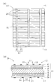
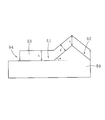
- (A) is a top view which shows the photovoltaic device concerning the 1st Embodiment of this invention
- (B) is AA arrow sectional drawing of FIG. 1 (A).
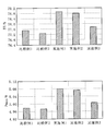
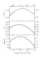
- 6 is a graph showing measurement results of Examples 1 to 3 and Comparative Examples 1 and 2. It is a graph which shows the measurement result of Example 4, 5. It is sectional drawing which shows the photovoltaic device which concerns on the 2nd Embodiment of this invention. It is a schematic diagram which shows the film thickness measuring method of the amorphous silicon thin film in an Example.
- (A) is a top view which shows the photovoltaic device which concerns on a prior art example
- (B) is BB arrow sectional drawing of FIG. 6 (A).
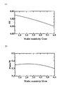
- (A) is a graph which shows the measurement result of FF (curve factor) of each photovoltaic device of Example 7
- (B) shows the measurement result of Pmax (maximum output) of each photovoltaic device of Example 7. It is a graph.
- the photovoltaic device 10 As shown in FIGS. 1A and 1B, the photovoltaic device 10 according to the first embodiment of the present invention includes a photovoltaic element 11, a first current collecting member 12, and a second current collecting member. 13.
- the first current collecting member 12 is stacked on one surface of the photovoltaic element 11 (upper side in FIG. 1).
- the second current collecting member 13 is laminated on the other surface (lower side in FIG. 1) of the photovoltaic element 11.
- the photovoltaic element 11 has a multilayered and plate-like structure.
- the photovoltaic element 11 includes an n-type crystal semiconductor substrate 14 and a first intrinsic amorphous system laminated in this order on the first current collecting member 12 side (the upper side in FIG. 1) of the n-type crystal semiconductor substrate 14.
- the silicon thin film 15, the p-type amorphous silicon thin film 16, the first transparent conductive film 17, and the n-type crystal semiconductor substrate 14 are stacked in this order on the second current collecting member 13 side (lower side in FIG. 1).
- the n-type crystal semiconductor substrate 14 is not particularly limited as long as it is a crystal having n-type semiconductor characteristics, and a known substrate can be used.
- Examples of the n-type crystal semiconductor composing the n-type crystal semiconductor substrate 14 include SiC, SiGe, SiN, etc. in addition to silicon (Si), but silicon is preferable from the viewpoint of productivity.
- the n-type crystal semiconductor substrate 14 may be a single crystal or a polycrystal.
- the upper and lower surfaces (one side and the other side) of the n-type crystal semiconductor substrate 14 are preferably subjected to uneven processing (not shown) in order to make light confinement due to diffused reflection of light more effective. For example, a large number of pyramidal irregularities can be formed by immersing the substrate material in an etching solution containing about 1 to 5% by mass of sodium hydroxide or potassium hydroxide.
- the n-type crystal semiconductor substrate 14 is preferably produced by an epitaxial growth method.
- the epitaxial growth method is a method of forming an epitaxial layer on a crystal substrate by supplying a source gas, for example.
- the formed epitaxial layer is separated from the crystal substrate and can be suitably used as the n-type crystal semiconductor substrate 14.
- the n-type crystal semiconductor substrate 14 produced by the epitaxial growth method has fewer oxygen-induced defects, less impurities, and contains a dopant with good reproducibility than those produced by a general Cz method or the like. There is an advantage that can be done.
- the maximum output and the like of the photovoltaic device 10 are increased and the uniformity thereof is increased. That is, since the difference in specific resistance between the substrates is small, mass production of the photovoltaic device 10 having desired output characteristics is facilitated. This effect is particularly prominent when the second current collecting member 13 side is a light incident surface (rear emitter type). Further, in the case of production by the Cz method, a silicon crystal is cut out to a desired thickness to obtain a substrate, so that silicon loss occurs during this cutting. This loss of silicon becomes more prominent as the substrate becomes thinner. However, in the case of the epitaxial growth method, since it can be directly produced to a desired thickness and it is not necessary to cut out, silicon loss does not occur and cost reduction is achieved.
- the specific resistance of the n-type crystal semiconductor substrate 14 is preferably 0.5 ⁇ cm to 5 ⁇ cm, and more preferably 1 ⁇ cm to 3 ⁇ cm.
- the maximum output and the like can be increased. This effect is remarkable when the rear emitter type is used. If the specific resistance is too small, the maximum output is reduced due to a decrease in bulk lifetime. If the specific resistance becomes too large, the lateral resistance on the side where the n-type amorphous silicon thin film 19 is formed increases, and the fill factor decreases. In addition, control of this specific resistance becomes easy by using the n-type crystal semiconductor substrate 14 produced by the epitaxial growth method.
- the thickness (average thickness) of the n-type crystal semiconductor substrate 14 is preferably 50 ⁇ m or more and 200 ⁇ m or less, and more preferably 80 ⁇ m or more and 150 ⁇ m or less. Thus, by using a relatively thin substrate, it is possible to improve the output characteristics and reduce the cost while exhibiting sufficient output characteristics.
- the first intrinsic amorphous silicon thin film 15 is stacked on the upper surface of the n-type crystal semiconductor substrate 14.
- the upper and lower surfaces do not limit the upper and lower sides during use (the same applies hereinafter).
- the film thickness of the first intrinsic amorphous silicon thin film 15 is not particularly limited, but can be, for example, 1 nm or more and 10 nm or less. When the film thickness is less than 1 nm, recombination of carriers is likely to occur due to defects easily occurring. Further, when the film thickness exceeds 10 nm, the fill factor is likely to be lowered.
- the first intrinsic amorphous silicon thin film 15 can be formed by a known method such as a chemical vapor deposition method (for example, a plasma CVD method).
- a chemical vapor deposition method for example, a plasma CVD method
- a mixed gas of SiH 4 and H 2 can be used as the source gas.
- the frequency is, for example, about 13.56 MHz or about 40.68 MHz, and more preferably about 40.68 MHz.
- the formation temperature is, for example, 100 ° C. or more and less than 300 ° C., and more preferably 180 ° C. or more and less than 220 ° C.
- the reaction pressure is 5 Pa or more and less than 300 Pa, and more preferably 50 Pa or more and less than 200 Pa.
- RF or VHF power is a 500 mW / cm less than 2, for example about 1 mW / cm 2 or more, less than about 5 mW / cm 2 or more 100 mW / cm 2 is more preferable.
- the p-type amorphous silicon thin film 16 is laminated on the upper surface of the first intrinsic amorphous silicon thin film 15.
- the film thickness of the p-type amorphous silicon thin film 16 is less than 6 nm, more preferably 5 nm or less, and further preferably 4 nm or less.
- the thickness of the p-type amorphous silicon thin film 16 is reduced as described above, and the first current collecting member 12 on the p-type amorphous silicon thin film 16 side of the p-type amorphous silicon thin film 16 side as described later.
- the lower limit of the thickness of the p-type amorphous silicon thin film 16 can be set to 1 nm, for example, and is preferably 2 nm, and more preferably 3 nm.
- Voc open voltage
- the fill factor can be further increased.
- the p-type amorphous silicon thin film 16 can also be formed by a known method such as a chemical vapor deposition method (for example, a plasma CVD method).
- a chemical vapor deposition method for example, a plasma CVD method
- a mixed gas of SiH 4 , H 2, and B 2 H 6 can be used as the source gas.
- the frequency is, for example, about 13.56 MHz or about 40.68 MHz, and more preferably about 40.68 MHz.
- the formation temperature is, for example, 100 ° C. or more and less than 300 ° C., and more preferably 130 ° C. or more and less than 200 ° C.
- the reaction pressure is 5 Pa or more and less than 300 Pa, and more preferably 50 Pa or more and less than 200 Pa.
- RF or VHF power is a 500 mW / cm less than 2, for example about 1 mW / cm 2 or more, less than about 5 mW / cm 2 or more 100 mW / cm 2 is more preferable.
- the first transparent conductive film 17 is laminated on the upper surface of the p-type amorphous silicon thin film 16.
- the transparent electrode material constituting the first transparent conductive film 17 include indium tin oxide (Indium Tin Oxide: ITO), tungsten doped indium oxide (Indium Tungsten Oxide: IWO), and cerium doped indium oxide (Indium).
- Well-known materials such as Cerium Oxide (ICO), IZO (Indium Zinc Oxide), AZO (aluminum-doped ZnO), and GZO (gallium-doped ZnO) can be exemplified.
- a method for forming the first transparent conductive film 17 is not particularly limited, and a known method such as a sputtering method, a vacuum deposition method, an ion plating method (reactive plasma deposition method), or the like can be used. It is preferable to use an ion plating method. By forming by an ion plating method in which high-energy particles are not generated, deterioration of the surface of the p-type amorphous silicon thin film 16 can be suppressed. Therefore, by doing in this way, the p-type amorphous silicon thin film 16 maintaining good quality can be used, and the fill factor can be further increased. Further, by using the ion plating method, the first transparent conductive film 17 having high adhesion can be formed, which is considered to be a cause of increasing the fill factor.
- the second intrinsic amorphous silicon thin film 18 is laminated on the lower surface of the n-type crystal semiconductor substrate 14.
- a preferable film thickness and film forming method of the second intrinsic amorphous silicon thin film 18 are the same as those of the first intrinsic amorphous silicon thin film 15.
- the n-type amorphous silicon thin film 19 is laminated on the lower surface of the second intrinsic amorphous silicon thin film 18.
- the film thickness of the n-type amorphous silicon thin film 19 is not particularly limited, but is preferably 1 nm or more and 20 nm or less, and more preferably 3 nm or more and 10 nm or less. By setting the film thickness in such a range, it is possible to reduce the short circuit current and the occurrence of carrier recombination in a balanced manner.
- the n-type amorphous silicon thin film 19 can also be formed by a known method such as a chemical vapor deposition method (for example, a plasma CVD method). In the case of the plasma CVD method, for example, a mixed gas of SiH 4 , H 2, and PH 3 can be used as the source gas.
- the frequency is, for example, about 13.56 MHz or about 40.68 MHz, and more preferably about 40.68 MHz.
- the formation temperature is, for example, 100 ° C. or more and less than 300 ° C., and more preferably 180 ° C. or more and less than 220 ° C.
- the reaction pressure is 5 Pa or more and less than 300 Pa, and more preferably 50 Pa or more and less than 200 Pa.
- RF or VHF power is a 500 mW / cm less than 2, for example about 1 mW / cm 2 or more, less than about 5 mW / cm 2 or more 100 mW / cm 2 is more preferable.
- the second transparent conductive film 20 is laminated on the lower surface of the n-type amorphous silicon thin film 19.
- the material and film forming method of the second transparent conductive film 20 are the same as those of the first transparent conductive film 17.
- transparent conductive films 17 and 20 are provided on both surfaces of the photovoltaic element 11, respectively. That is, a transparent conductive film is also laminated on the side where light does not enter.
- the transparent electrode films 17 and 20 between the p-type amorphous silicon thin film 16 or the n-type amorphous silicon thin film 19 and the current collecting members 12 and 13, the interface state is increased. Can be suppressed, and the fill factor can be increased.
- the first current collecting member 12 is laminated on the upper surface of the photovoltaic element 11, that is, the upper surface of the first transparent conductive film 17.
- the first current collecting member 12 includes a plurality of bus bar electrodes (I) 21 formed in parallel to each other and a plurality of finger electrodes (I) 22 connected to the bus bar electrodes (I) 21 and formed in parallel to each other. Have.
- the plurality of bus bar electrodes (I) 21 are arranged at equal intervals.
- the bus bar electrode (I) 21 has a linear shape or a strip shape, and is made of a conductive material.
- a conductive adhesive such as a silver paste, a metal conductive wire such as a copper wire, or a combination of a conductive adhesive and a metal copper wire can be used.
- This metal conductive wire can be fixed on the first transparent conductive film 17 using a conductive or non-conductive fixing adhesive or a low melting point metal (solder or the like).
- the bus bar electrode (I) 21 can be formed by a printing method such as screen printing or gravure offset printing.
- each bus bar electrode (I) 21 is, for example, about 0.5 mm to 2 mm when the number is 3 to 5. Moreover, when the number of each bus-bar electrode (I) 21 is 10 or more, a wire with a diameter of about 0.1 mm can also be used.
- the finger electrode (I) 22 is linear and is formed of a conductive material.
- the finger electrode (I) 22 is provided orthogonal to the bus bar electrode (I) 21.
- the plurality of finger electrodes (I) 22 are arranged at equal intervals.
- the conductive material forming the finger electrode (I) 22 is the same as that constituting the bus bar electrode (I) 21.
- the bus bar electrode (I) 21 and the finger electrode (I) 22 are both formed of a conductive adhesive, they can be simultaneously laminated on one surface of the first transparent conductive film 17 by printing.
- the width of each finger electrode (I) 22 is, for example, about 10 ⁇ m to 300 ⁇ m, preferably 30 ⁇ m to 200 ⁇ m.
- the interval (S1) between adjacent finger electrodes (I) 22 is less than 2 mm, and preferably 1.5 mm or less.
- each region defined by the first current collecting member 12 is the first transparent conductive film 17 (photovoltaic power generation). It becomes the non-laminated region 25 of the first current collecting member 12 on the surface of the element 11).
- the surface of the first transparent conductive film 17 (photovoltaic element 11) refers to the surface on which the first current collecting member 12 is laminated.
- Each non-stacked region 25 has a rectangular shape (band shape) in which the length direction of the finger electrode (I) 22 is the length direction.
- the interval (S 1) between the finger electrodes (I) 22 is the maximum width of the non-laminated region 25 of the first current collecting member 12 on the surface of the first transparent conductive film 17.
- the fill factor is reduced by narrowing the distance (S 1) between the finger electrodes (I) 22 on the p-type amorphous silicon thin film 16 side to less than 2 mm with respect to the pn junction portion.
- the power generation efficiency can be increased.
- the lower limit of the distance (S1) between the finger electrodes (I) 22 is not particularly limited, but is preferably 0.1 mm, for example, and more preferably 0.5 mm.
- the interval (S1) between the finger electrodes (I) 22 on the p-type amorphous silicon thin film 16 side is also sufficiently used as the light incident surface. Moreover, the usage-amount of the electroconductive material which forms finger electrode (I) 22 can be reduced.
- the second current collecting member 13 is provided on the lower surface of the photovoltaic element 11, that is, on the surface of the second transparent conductive film 20.
- the second current collecting member 13 includes a plurality of bus bar electrodes (II) (not shown) formed in parallel to each other, and a plurality of finger electrodes connected to the bus bar electrodes (II) at right angles and formed in parallel to each other. (II) 24.
- the shape, material, size, formation method, and the like of the bus bar electrode (II) of the second current collecting member 13 are the same as those of the bus bar electrode (I) 21 of the first current collecting member 12.
- the shape, material, size, formation method, and the like of the finger electrode (II) 24 are the same as those of the finger electrode (I) 22 of the first current collecting member 12.
- the interval (S2) between the adjacent finger electrodes (II) 24 is not particularly limited.
- the distance (S2) can be, for example, 0.5 mm or more and 4 mm or less, and is preferably 1 mm or more, more preferably 2 mm or more, and particularly preferably greater than 2 mm. Moreover, 3 mm or less, Furthermore, less than 3 mm, especially 2.5 mm or less are preferable.
- the second current collecting member 13 side can be suitably used as the light incident surface.
- the amount of the conductive material forming the finger electrode (II) 24 can be reduced.
- Photovoltaic generators 10 having such a structure are usually used by connecting a plurality thereof in series. By using a plurality of photovoltaic power generation devices 10 connected in series, the generated voltage can be increased.
- the thickness of the p-type amorphous silicon thin film 16 is reduced to less than 6 nm, and the distance (S1) between the finger electrodes (I) 22, that is, the first By narrowing the maximum width of the non-laminated region 25 of the first current collecting member 12 on the surface of the transparent conductive film 17 to be less than 2 mm, the fill factor is increased and the power generation efficiency can be increased.
- the light incident surface may be any, but the second current collecting member 13 side can be used as the light incident surface.
- the interval (S2) can be sufficiently widened to reduce the light shielding property.
- the power generation efficiency of the photovoltaic device 10 can be improved more.
- the thickness of the p-type amorphous silicon thin film 16 is reduced, and the first current collecting member 12 side can be used as the light incident surface.
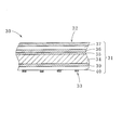
- the photovoltaic device 30 As shown in FIG. 4, the photovoltaic device 30 according to the second embodiment of the present invention includes a photovoltaic element 31, a first current collecting member 32 that is stacked on the upper surface and the lower surface of the photovoltaic element 31, and A second current collecting member 33 is provided.
- the photovoltaic element 31 includes an n-type crystal semiconductor substrate 34, a first intrinsic amorphous silicon thin film 35 stacked in this order on the first current collecting member 32 side of the n-type crystal semiconductor substrate 34, and a p-type non-layer.
- the photovoltaic element 31 is the same as the photovoltaic element 11 of FIG. 1 except that it does not have the second intrinsic amorphous silicon thin film.
- the shape, material, film forming method, and the like of the transparent conductive film 40 in FIG. 2 are respectively the n-type crystal semiconductor substrate 14, the first intrinsic amorphous silicon thin film 15, the p-type amorphous silicon thin film 16 in FIG. Since it is the same as that of the first transparent conductive film 17, the n-type amorphous silicon thin film 19, and the second transparent conductive film 20, detailed description thereof is omitted.
- the photovoltaic device 30 has a structure in which an n-type crystal semiconductor substrate 34 and an n-type amorphous silicon thin film 39 are directly bonded. As described above, a sufficient fill factor can be obtained without stacking the second intrinsic amorphous silicon thin film between the n-type crystal semiconductor substrate 34 and the n-type amorphous silicon thin film 39.
- the first current collecting member 32 laminated on the upper surface of the photovoltaic element 31 (the surface of the first transparent conductive film 37) is a metal film.
- the metal film (first current collecting member 32) is laminated on substantially the entire surface (substantially the entire surface). That is, the maximum width of the non-laminated region of the first current collecting member 32 on the surface of the first transparent conductive film 37 (the surface on the side where the first current collecting member 32 is laminated) is 0 mm (the non-laminated region is Absence).
- the metal film can be formed by a thin film forming method such as PVD or CVD.
- the electrical conductivity of the metal film obtained by the thin film formation method is generally larger than that by the printing method, and as a result, the amount of metal material used to form the metal film (first current collecting member 32) is reduced. It can also be reduced.
- This metal film can be formed of a known metal such as Ag, Al, Cu, Ni, Cr, or the like, and can also be formed of an alloy containing one or more of these metals. Furthermore, it can also be set as the structure which laminated
- This metal film is preferably made of Ag.
- the thickness of the metal film can be, for example, 100 nm or more and 1000 nm or less, and more preferably less than 500 nm for cost reduction.
- This metal film is preferably formed by vacuum deposition, sputtering, or the like.
- the second current collecting member 33 laminated on the lower surface of the photovoltaic element 31 (the surface of the second transparent conductive film 40) has a shape composed of a bus bar electrode and a finger electrode.
- the shape, material, size, formation method, and the like of the second current collecting member 33 are the same as those of the second current collecting member 13 in FIG.
- the second current collecting member 33 side is a light incident surface.
- the present invention is not limited to the above-described embodiment, and the configuration thereof can be changed without changing the gist of the present invention.
- the second current collecting member is not a structure composed of bus bar electrodes and finger electrodes, but a metal film in which a conductive material is laminated on substantially the entire surface (substantially the entire surface). It can also be set as the structure which consists of.
- the conductive material for forming the metal film include known metals such as Ag, Al, Cu, Ni, and Cr, and alloys thereof. Ag that has high reflectivity at wavelengths in the infrared region is used. It is preferable.
- the thickness of the metal film can be, for example, 100 nm or more and 1000 nm or less, and more preferably less than 500 nm for cost reduction.
- the metal film can be formed by vacuum deposition, sputtering, or the like. By doing in this way, the current collection efficiency by the side of the 2nd current collection member can be raised. In this case, the first current collecting member side is used as the light incident surface.
- the shape of the first current collecting member is not particularly limited as long as the maximum width of the non-stacked region is less than 2 mm.
- the first current collecting member may be a metal film having a hole having a diameter of less than 2 mm, or may be formed of only bus bar electrodes arranged at intervals of less than 2 mm.
- Examples 1 to 3 and Comparative Examples 1 and 2> A first intrinsic amorphous silicon thin film, a p-type amorphous silicon thin film, and a first transparent conductive film were laminated in this order on one side of an n-type single crystal silicon substrate manufactured by the Cz method.
- the first intrinsic amorphous silicon thin film is 7 nm thick by chemical vapor deposition
- the p-type amorphous silicon thin film is 5 nm thick by chemical vapor deposition
- the first transparent conductive film is an ion.
- a film was formed by a plating method.
- a second intrinsic amorphous silicon thin film, an n-type amorphous silicon thin film, and a second transparent conductive film were laminated in this order on the other side of the n-type single crystal silicon substrate.
- the second intrinsic amorphous silicon thin film is 7 nm thick by chemical vapor deposition
- the n-type amorphous silicon thin film is 5 nm thick by chemical vapor deposition
- the second transparent conductive film is an ion.
- a film was formed by a plating method.
- the transparent electrode material constituting the first and second transparent conductive films IWO was used.
- a plurality of parallel bus bar electrodes and a plurality of finger electrodes respectively orthogonal to the bus bar electrodes were formed as current collecting members on both surfaces of the photovoltaic device thus obtained.
- the current collecting member was formed by printing using a silver paste.
- the intervals between the finger electrode (I) on the p-type amorphous silicon thin film side and the finger electrode (II) on the n-type amorphous silicon thin film side were as follows.
- the photovoltaic power generators of Examples 1 to 3 and Comparative Examples 1 and 2 were obtained.
- the width of the finger electrode was 50 ⁇ m or more and less than 100 ⁇ m.
- Comparative Example 1 Distance between finger electrodes (I) on the p-type amorphous silicon thin film side: 2 mm Distance between finger electrodes (II) on the n-type amorphous silicon thin film side: 2 mm Comparative Example 2: Distance between finger electrodes (I) on the p-type amorphous silicon thin film side: 2 mm n-type amorphous silicon thin film side finger electrode (II) spacing: 1.5 mm
- Example 1 Distance between finger electrodes (I) on the p-type amorphous silicon thin film side: 1.5 mm Distance between finger electrodes (II) on the n-type amorphous silicon thin film side: 2 mm
- Example 2 Interval between finger electrodes (I) on the p-type amorphous silicon thin film side: 1.5 mm Distance between finger electrodes (II) on the n-type amorphous silicon thin film side: 2.5 mm
- Example 3 Distance between finger electrodes (I) on the p-type amorphous silicon thin film side: 1.5
- the fill factor (FF) and maximum output (Pmax) of each obtained photovoltaic device were measured.
- the p-type amorphous silicon thin film side (first current collecting member side) was used as the light incident surface. Further, the area of the portion where the first current collecting member on the light incident surface side is not laminated (the portion where the light is incident) is made equal. That is, in the screen used for printing, the width of the finger electrodes was adjusted together with the interval between the finger electrodes so that the light incident areas became equal. The measurement results are shown in FIG.
- Narrowing the gap between the finger electrodes (II) on the n-type amorphous silicon thin film side does not improve the fill factor, etc., and the finger electrode (I) on the p-type amorphous silicon thin film side is less than 2 mm.
- the fill factor and the like are improved, and that the fill factor and the like are not greatly reduced even when the interval between the finger electrodes (II) on the n-type amorphous silicon thin film side is widened.
- Example 4 The distance between the finger electrode (I) on the p-type amorphous silicon thin film side and the finger electrode (II) on the n-type amorphous silicon thin film side and the film thickness of the p-type amorphous silicon thin film are as follows: A photovoltaic device of Example 4 was obtained in the same manner as Example 1 except that. Interval between finger electrodes (I) on the p-type amorphous silicon thin film side: 1 mm Distance between finger electrodes (II) on the n-type amorphous silicon thin film side: 2 mm Thickness of p-type amorphous silicon thin film (layer thickness): 1 nm to 8 Varyed between nm. In addition, 6 nm or more is a comparative example.
- the first current collecting member on the p-type amorphous silicon thin film side is formed by vacuum deposition, has a thickness of 100 nm, and is provided so as to cover almost the entire surface.
- the distance between the finger electrodes (II) on the n-type amorphous silicon thin film side and the thickness of the p-type amorphous silicon thin film are as follows.
- a photovoltaic device of Example 5 (a photovoltaic device having the shape shown in FIG. 4) was obtained in the same manner as in Example 1 except that the crystalline silicon thin film was not laminated.
- the thickness of the p-type amorphous silicon thin film was changed between 1 nm and 8 nm. In addition, 6 nm or more is a comparative example.
- the open circuit voltage (V oc ), fill factor (FF), and maximum output (Pmax) of the photovoltaic devices obtained in Example 4 and Example 5 were measured.
- the n-type amorphous silicon thin film side (second current collecting member side) was used as the light incident surface.
- the measurement results are shown in FIG. In FIG. 3, the solid line is Example 4, and the broken line is Example 5.
- Demonstrating a high fill factor and maximum output by setting the thickness of the p-type amorphous silicon thin film to less than 6 nm, and forming the first current collecting member on the p-type amorphous silicon thin film side by vacuum deposition It can be seen that an even higher fill factor and maximum output can be achieved by forming an Ag metal layer having a thickness of 100 nm.
- Comparative Example 3 An IWO film: 100 nm was formed by ion plating on a smooth glass substrate that was not subjected to uneven processing for light confinement.
- Comparative Example 4 i-type amorphous silicon thin film: 7 nm and p-type amorphous silicon thin film: 5 nm on a smooth glass substrate not subjected to concave and convex processing for light confinement, in order using the CVD method And an ion plating method were used to form an IWO film of 100 nm.
- Comparative Example 5 An i-type amorphous silicon thin film: 7 nm and an n-type amorphous silicon thin film: 5 nm on a smooth glass substrate not subjected to uneven processing for light confinement, in order using the CVD method. And an ion plating method were used to form an IWO film of 100 nm. Comparative Example 6: An IWO film: 100 nm was formed by ion plating on a smooth n-type single crystal silicon substrate (200 ⁇ m, 1 to 2 ⁇ cm) on which unevenness processing for light confinement was not performed.
- Comparative Example 7 i-type amorphous silicon thin film: 7 nm on a smooth n-type single crystal silicon substrate (200 ⁇ m, 1 to 2 ⁇ cm) not subjected to concave and convex processing for light confinement using CVD in order And an p-type amorphous silicon thin film: 5 nm and an IWO film: 100 nm were formed using an ion plating method.
- Reference Example 1 An i-type amorphous silicon thin film: 7 nm on a smooth n-type single crystal silicon substrate (200 ⁇ m, 1 to 2 ⁇ cm) not subjected to uneven processing for light confinement using CVD in order. And an n-type amorphous silicon thin film: 5 nm and an ion plating method were used to form an IWO film: 100 nm. Table 1 shows the sheet resistance measurement results for each test membrane.
- the results in Table 1 suggest that the lateral resistance on the p-type amorphous silicon thin film forming surface side is determined by the transparent conductive film.
- the volume resistance of the transparent conductive film on the p-type amorphous silicon thin film forming surface side is less than 1.5 ⁇ 10 ⁇ 4 ⁇ cm
- the p-type amorphous silicon thin film forming surface in the present invention It is expected that an effect equivalent to the improvement of the fill factor can be obtained by setting the distance between the finger electrodes on the side to less than 2 mm.
- improvement in carrier density increases light absorption loss in the transparent conductive film.
- the lateral resistance can also be reduced by increasing the thickness of the transparent conductive film on the p-type amorphous silicon thin film forming surface side.
- it is effective to improve the current characteristics to select a film thickness at which the spectral intensity of sunlight is high and the reflectance at 400 to 600 nm is low. Only an increase of about 10 nm is allowed. For this reason, it is difficult to dramatically reduce the lateral resistance.
- the absorption loss in the transparent conductive film increases in proportion to the increase in thickness of the transparent conductive film on the opposite side.
- increasing the thickness of the transparent conductive film is not preferable from the viewpoint of productivity and cost reduction. Therefore, increasing the fill factor by reducing the distance between the finger electrodes provided on the p-type amorphous silicon thin film side is better than increasing the fill factor by reducing the resistance of the transparent conductive film. From the standpoints of productivity and cost reduction.
- Example 6 Photovoltaic generation of Example 6 in the same manner as in Example 5 except that an n-type single crystal silicon substrate (thickness 150 ⁇ m) produced by the epitaxial growth method was used and the thermal donor killer annealing step for this substrate was omitted. An element was obtained. The film thickness of the p-type amorphous silicon thin film was 5 nm.
- the thermal donor killer annealing process is a technique for removing the thermal donor in the n-type single crystal silicon substrate, and is particularly important for a heterojunction element in a low temperature process. In other examples and comparative examples using an n-type single crystal silicon substrate manufactured by the Cz method, this thermal donor killer annealing process is performed. By omitting this step, the manufacturing cost can be further reduced.
- the photovoltaic device obtained in Example 6 had a maximum output (Pmax) of 5.27 W and a fill factor (FF) of 81%.
- Example 7 A photovoltaic device was obtained in the same manner as in Example 5 using an n-type single crystal silicon substrate (Cz method) having a specific resistance of 0.3 to 6 ⁇ cm.
- the film thickness of the p-type amorphous silicon thin film was 5 nm.
- the measurement results of FF (curve factor) and Pmax (maximum output) of each obtained photovoltaic device are shown in FIGS.
- FIG. 7A As shown in FIG. 7A, as the specific resistance increases, the effective lateral resistance on the n-layer amorphous silicon thin film forming surface side increases and FF (curve factor) decreases.
- Pmax maximum output
- Pmax has a good range of 0.5-5 ⁇ cm because the advantages of FF improvement accompanying the decrease in specific resistance compete with the disadvantages of reducing bulk lifetime.
- the range of 1 to 3 ⁇ cm is particularly good. Since the epitaxial substrate has very few oxygen defects and the specific resistance can be controlled only at the doping level, this good range can be accurately aimed.
- a virtual substrate 50 having both the smooth part 51 and the uneven part 52 is shown in FIG.
- TEM transmission electron microscope
- the thickness t perpendicular to the substrate 50, the thickness t ′ perpendicular to the plane, and the angle ⁇ of the concavo-convex portion 52 can be measured.
- the film thickness of the amorphous silicon thin film 53 laminated on the smooth portion 51 indicates t
- the film thickness of the amorphous silicon thin film 53 laminated on the uneven portion 52 indicates t ′.
- a film thickness evaluation method using a stylus step meter or the like that can shorten the measurement time and is simple.
- the stylus profilometer is a device that measures the needle up and down according to the level difference of the sample by touching the sample with the needle and tracing the surface horizontally on the sample with a level difference. .
Abstract
Priority Applications (6)
| Application Number | Priority Date | Filing Date | Title |
|---|---|---|---|
| US14/777,800 US20160300967A1 (en) | 2013-03-19 | 2014-03-14 | Photovoltaic device |
| CN201480017109.4A CN105103307B (zh) | 2013-03-19 | 2014-03-14 | 光发电装置 |
| JP2014527413A JP5755372B2 (ja) | 2013-03-19 | 2014-03-14 | 光発電装置 |
| AU2014239715A AU2014239715A1 (en) | 2013-03-19 | 2014-03-14 | Photovoltaic device |
| KR1020157029978A KR20150132545A (ko) | 2013-03-19 | 2014-03-14 | 광 발전 장치 |
| EP14769613.2A EP2978028A4 (fr) | 2013-03-19 | 2014-03-14 | Dispositif photovoltaïque |
Applications Claiming Priority (2)
| Application Number | Priority Date | Filing Date | Title |
|---|---|---|---|
| JP2013-056713 | 2013-03-19 | ||
| JP2013056713 | 2013-03-19 |
Publications (1)
| Publication Number | Publication Date |
|---|---|
| WO2014148392A1 true WO2014148392A1 (fr) | 2014-09-25 |
Family
ID=51580076
Family Applications (1)
| Application Number | Title | Priority Date | Filing Date |
|---|---|---|---|
| PCT/JP2014/056939 WO2014148392A1 (fr) | 2013-03-19 | 2014-03-14 | Dispositif photovoltaïque |
Country Status (8)
| Country | Link |
|---|---|
| US (1) | US20160300967A1 (fr) |
| EP (1) | EP2978028A4 (fr) |
| JP (1) | JP5755372B2 (fr) |
| KR (1) | KR20150132545A (fr) |
| CN (1) | CN105103307B (fr) |
| AU (1) | AU2014239715A1 (fr) |
| TW (1) | TW201448245A (fr) |
| WO (1) | WO2014148392A1 (fr) |
Cited By (3)
| Publication number | Priority date | Publication date | Assignee | Title |
|---|---|---|---|---|
| JP2016164930A (ja) * | 2015-03-06 | 2016-09-08 | シャープ株式会社 | 光電変換素子およびその製造方法 |
| KR101799580B1 (ko) | 2016-12-16 | 2017-11-20 | 엘지전자 주식회사 | 이종 접합 태양전지 |
| JP2019004135A (ja) * | 2017-06-14 | 2019-01-10 | エルジー エレクトロニクス インコーポレイティド | 太陽電池、太陽電池モジュール及びその製造方法 |
Families Citing this family (4)
| Publication number | Priority date | Publication date | Assignee | Title |
|---|---|---|---|---|
| WO2016084299A1 (fr) * | 2014-11-28 | 2016-06-02 | パナソニックIpマネジメント株式会社 | Cellule solaire et module solaire |
| CN107634111A (zh) * | 2016-07-15 | 2018-01-26 | 新日光能源科技股份有限公司 | 太阳能电池 |
| JP7064823B2 (ja) * | 2016-08-31 | 2022-05-11 | 株式会社マテリアル・コンセプト | 太陽電池及びその製造方法 |
| TWI617041B (zh) * | 2016-12-02 | 2018-03-01 | 財團法人金屬工業研究發展中心 | 矽基異質接面太陽能電池及其製造方法 |
Citations (5)
| Publication number | Priority date | Publication date | Assignee | Title |
|---|---|---|---|---|
| JPH0531007B2 (fr) | 1984-11-21 | 1993-05-11 | Bendix France | |
| JP2009290234A (ja) * | 2009-09-07 | 2009-12-10 | Sanyo Electric Co Ltd | 光起電力素子 |
| JP2010103514A (ja) * | 2008-09-29 | 2010-05-06 | Semiconductor Energy Lab Co Ltd | Soi基板の作製方法及び単結晶半導体層の作製方法 |
| JP2010272897A (ja) * | 2010-09-08 | 2010-12-02 | Sanyo Electric Co Ltd | 太陽電池モジュール |
| JP2012158273A (ja) * | 2011-02-02 | 2012-08-23 | Panasonic Corp | 太陽電池を搭載した自転車 |
Family Cites Families (10)
| Publication number | Priority date | Publication date | Assignee | Title |
|---|---|---|---|---|
| JP2001274427A (ja) * | 2000-03-28 | 2001-10-05 | Sanyo Electric Co Ltd | 光起電力素子及びその製造方法 |
| US7619159B1 (en) * | 2002-05-17 | 2009-11-17 | Ugur Ortabasi | Integrating sphere photovoltaic receiver (powersphere) for laser light to electric power conversion |
| JP4229858B2 (ja) * | 2004-03-16 | 2009-02-25 | 三洋電機株式会社 | 光電変換装置 |
| US20070235077A1 (en) * | 2006-03-27 | 2007-10-11 | Kyocera Corporation | Solar Cell Module and Manufacturing Process Thereof |
| US20110132423A1 (en) * | 2006-10-11 | 2011-06-09 | Gamma Solar | Photovoltaic solar module comprising bifacial solar cells |
| JP5526461B2 (ja) * | 2007-03-19 | 2014-06-18 | 三洋電機株式会社 | 光起電力装置 |
| JP5384224B2 (ja) * | 2009-06-29 | 2014-01-08 | 三洋電機株式会社 | 太陽電池 |
| TW201130148A (en) * | 2009-09-18 | 2011-09-01 | Sanyo Electric Co | Solar battery cell, solar battery module, and solar battery system |
| JP5535709B2 (ja) * | 2010-03-19 | 2014-07-02 | 三洋電機株式会社 | 太陽電池、その太陽電池を用いた太陽電池モジュール及び太陽電池の製造方法 |
| JP5379767B2 (ja) * | 2010-09-02 | 2013-12-25 | PVG Solutions株式会社 | 太陽電池セルおよびその製造方法 |
-
2014
- 2014-03-14 CN CN201480017109.4A patent/CN105103307B/zh not_active Expired - Fee Related
- 2014-03-14 US US14/777,800 patent/US20160300967A1/en not_active Abandoned
- 2014-03-14 AU AU2014239715A patent/AU2014239715A1/en not_active Abandoned
- 2014-03-14 JP JP2014527413A patent/JP5755372B2/ja not_active Expired - Fee Related
- 2014-03-14 WO PCT/JP2014/056939 patent/WO2014148392A1/fr active Application Filing
- 2014-03-14 EP EP14769613.2A patent/EP2978028A4/fr not_active Withdrawn
- 2014-03-14 KR KR1020157029978A patent/KR20150132545A/ko not_active Application Discontinuation
- 2014-03-18 TW TW103110139A patent/TW201448245A/zh unknown
Patent Citations (5)
| Publication number | Priority date | Publication date | Assignee | Title |
|---|---|---|---|---|
| JPH0531007B2 (fr) | 1984-11-21 | 1993-05-11 | Bendix France | |
| JP2010103514A (ja) * | 2008-09-29 | 2010-05-06 | Semiconductor Energy Lab Co Ltd | Soi基板の作製方法及び単結晶半導体層の作製方法 |
| JP2009290234A (ja) * | 2009-09-07 | 2009-12-10 | Sanyo Electric Co Ltd | 光起電力素子 |
| JP2010272897A (ja) * | 2010-09-08 | 2010-12-02 | Sanyo Electric Co Ltd | 太陽電池モジュール |
| JP2012158273A (ja) * | 2011-02-02 | 2012-08-23 | Panasonic Corp | 太陽電池を搭載した自転車 |
Non-Patent Citations (1)
| Title |
|---|
| See also references of EP2978028A4 |
Cited By (4)
| Publication number | Priority date | Publication date | Assignee | Title |
|---|---|---|---|---|
| JP2016164930A (ja) * | 2015-03-06 | 2016-09-08 | シャープ株式会社 | 光電変換素子およびその製造方法 |
| KR101799580B1 (ko) | 2016-12-16 | 2017-11-20 | 엘지전자 주식회사 | 이종 접합 태양전지 |
| JP2019004135A (ja) * | 2017-06-14 | 2019-01-10 | エルジー エレクトロニクス インコーポレイティド | 太陽電池、太陽電池モジュール及びその製造方法 |
| JP7300245B2 (ja) | 2017-06-14 | 2023-06-29 | シャンラオ ジンコ ソーラー テクノロジー デベロップメント シーオー.,エルティーディー | 太陽電池、太陽電池モジュール及びその製造方法 |
Also Published As
| Publication number | Publication date |
|---|---|
| KR20150132545A (ko) | 2015-11-25 |
| EP2978028A1 (fr) | 2016-01-27 |
| TW201448245A (zh) | 2014-12-16 |
| JPWO2014148392A1 (ja) | 2017-02-16 |
| AU2014239715A1 (en) | 2015-11-05 |
| JP5755372B2 (ja) | 2015-07-29 |
| CN105103307B (zh) | 2017-05-24 |
| EP2978028A4 (fr) | 2016-10-26 |
| CN105103307A (zh) | 2015-11-25 |
| US20160300967A1 (en) | 2016-10-13 |
Similar Documents
| Publication | Publication Date | Title |
|---|---|---|
| JP5755372B2 (ja) | 光発電装置 | |
| US10084107B2 (en) | Transparent conducting oxide for photovoltaic devices | |
| JP2017130664A (ja) | 太陽電池 | |
| JP5869674B2 (ja) | 光発電素子 | |
| JP2016111357A5 (fr) | ||
| JP5642355B2 (ja) | 太陽電池モジュール | |
| JP2017139267A (ja) | 太陽電池素子および太陽電池モジュール | |
| WO2011093380A1 (fr) | Cellule solaire et module de cellules solaires utilisant ladite cellule solaire | |
| CN107735866B (zh) | 太阳能电池 | |
| JP2016029675A (ja) | 薄膜太陽電池用透光性絶縁基板、及び集積型薄膜シリコン太陽電池 | |
| JP2019033201A (ja) | 結晶シリコン系太陽電池 | |
| WO2015050163A1 (fr) | Élément photovoltaïque | |
| KR20130035876A (ko) | 광전 변환 장치 | |
| JP5987127B1 (ja) | 光発電素子及びその製造方法 | |
| JP2014216334A (ja) | 光発電素子 | |
| WO2018055847A1 (fr) | Cellule solaire et son procédé de fabrication, et module de cellule solaire | |
| TWI573284B (zh) | 太陽能電池、其模組及其製造方法 | |
| WO2015050161A1 (fr) | Élément photovoltaïque | |
| JP2011216586A (ja) | 積層型光電変換装置および積層型光電変換装置の製造方法 | |
| JP5909662B2 (ja) | 太陽電池モジュール | |
| JP2012060166A (ja) | 光電変換装置 | |
| JP2014216335A (ja) | 光発電素子 | |
| JP2013058743A (ja) | 薄膜光電変換素子 |
Legal Events
| Date | Code | Title | Description |
|---|---|---|---|
| WWE | Wipo information: entry into national phase |
Ref document number: 201480017109.4 Country of ref document: CN |
|
| ENP | Entry into the national phase |
Ref document number: 2014527413 Country of ref document: JP Kind code of ref document: A |
|
| 121 | Ep: the epo has been informed by wipo that ep was designated in this application |
Ref document number: 14769613 Country of ref document: EP Kind code of ref document: A1 |
|
| WWE | Wipo information: entry into national phase |
Ref document number: 14777800 Country of ref document: US |
|
| NENP | Non-entry into the national phase |
Ref country code: DE |
|
| WWE | Wipo information: entry into national phase |
Ref document number: 2014769613 Country of ref document: EP |
|
| ENP | Entry into the national phase |
Ref document number: 20157029978 Country of ref document: KR Kind code of ref document: A |
|
| ENP | Entry into the national phase |
Ref document number: 2014239715 Country of ref document: AU Date of ref document: 20140314 Kind code of ref document: A |