WO2014034161A1 - 基板支持装置、及び露光装置 - Google Patents
基板支持装置、及び露光装置 Download PDFInfo
- Publication number
- WO2014034161A1 WO2014034161A1 PCT/JP2013/057062 JP2013057062W WO2014034161A1 WO 2014034161 A1 WO2014034161 A1 WO 2014034161A1 JP 2013057062 W JP2013057062 W JP 2013057062W WO 2014034161 A1 WO2014034161 A1 WO 2014034161A1
- Authority
- WO
- WIPO (PCT)
- Prior art keywords
- substrate
- pattern
- exposure
- light
- outer peripheral
- Prior art date
- Legal status (The legal status is an assumption and is not a legal conclusion. Google has not performed a legal analysis and makes no representation as to the accuracy of the status listed.)
- Ceased
Links
Images




Classifications
-
- G—PHYSICS
- G03—PHOTOGRAPHY; CINEMATOGRAPHY; ANALOGOUS TECHNIQUES USING WAVES OTHER THAN OPTICAL WAVES; ELECTROGRAPHY; HOLOGRAPHY
- G03F—PHOTOMECHANICAL PRODUCTION OF TEXTURED OR PATTERNED SURFACES, e.g. FOR PRINTING, FOR PROCESSING OF SEMICONDUCTOR DEVICES; MATERIALS THEREFOR; ORIGINALS THEREFOR; APPARATUS SPECIALLY ADAPTED THEREFOR
- G03F7/00—Photomechanical, e.g. photolithographic, production of textured or patterned surfaces, e.g. printing surfaces; Materials therefor, e.g. comprising photoresists; Apparatus specially adapted therefor
- G03F7/20—Exposure; Apparatus therefor
- G03F7/24—Curved surfaces
-
- G—PHYSICS
- G03—PHOTOGRAPHY; CINEMATOGRAPHY; ANALOGOUS TECHNIQUES USING WAVES OTHER THAN OPTICAL WAVES; ELECTROGRAPHY; HOLOGRAPHY
- G03F—PHOTOMECHANICAL PRODUCTION OF TEXTURED OR PATTERNED SURFACES, e.g. FOR PRINTING, FOR PROCESSING OF SEMICONDUCTOR DEVICES; MATERIALS THEREFOR; ORIGINALS THEREFOR; APPARATUS SPECIALLY ADAPTED THEREFOR
- G03F1/00—Originals for photomechanical production of textured or patterned surfaces, e.g., masks, photo-masks, reticles; Mask blanks or pellicles therefor; Containers specially adapted therefor; Preparation thereof
- G03F1/38—Masks having auxiliary features, e.g. special coatings or marks for alignment or testing; Preparation thereof
- G03F1/42—Alignment or registration features, e.g. alignment marks on the mask substrates
-
- G—PHYSICS
- G03—PHOTOGRAPHY; CINEMATOGRAPHY; ANALOGOUS TECHNIQUES USING WAVES OTHER THAN OPTICAL WAVES; ELECTROGRAPHY; HOLOGRAPHY
- G03F—PHOTOMECHANICAL PRODUCTION OF TEXTURED OR PATTERNED SURFACES, e.g. FOR PRINTING, FOR PROCESSING OF SEMICONDUCTOR DEVICES; MATERIALS THEREFOR; ORIGINALS THEREFOR; APPARATUS SPECIALLY ADAPTED THEREFOR
- G03F7/00—Photomechanical, e.g. photolithographic, production of textured or patterned surfaces, e.g. printing surfaces; Materials therefor, e.g. comprising photoresists; Apparatus specially adapted therefor
- G03F7/20—Exposure; Apparatus therefor
-
- G—PHYSICS
- G03—PHOTOGRAPHY; CINEMATOGRAPHY; ANALOGOUS TECHNIQUES USING WAVES OTHER THAN OPTICAL WAVES; ELECTROGRAPHY; HOLOGRAPHY
- G03F—PHOTOMECHANICAL PRODUCTION OF TEXTURED OR PATTERNED SURFACES, e.g. FOR PRINTING, FOR PROCESSING OF SEMICONDUCTOR DEVICES; MATERIALS THEREFOR; ORIGINALS THEREFOR; APPARATUS SPECIALLY ADAPTED THEREFOR
- G03F9/00—Registration or positioning of originals, masks, frames, photographic sheets or textured or patterned surfaces, e.g. automatically
- G03F9/70—Registration or positioning of originals, masks, frames, photographic sheets or textured or patterned surfaces, e.g. automatically for microlithography
- G03F9/7073—Alignment marks and their environment
-
- G—PHYSICS
- G03—PHOTOGRAPHY; CINEMATOGRAPHY; ANALOGOUS TECHNIQUES USING WAVES OTHER THAN OPTICAL WAVES; ELECTROGRAPHY; HOLOGRAPHY
- G03F—PHOTOMECHANICAL PRODUCTION OF TEXTURED OR PATTERNED SURFACES, e.g. FOR PRINTING, FOR PROCESSING OF SEMICONDUCTOR DEVICES; MATERIALS THEREFOR; ORIGINALS THEREFOR; APPARATUS SPECIALLY ADAPTED THEREFOR
- G03F9/00—Registration or positioning of originals, masks, frames, photographic sheets or textured or patterned surfaces, e.g. automatically
- G03F9/70—Registration or positioning of originals, masks, frames, photographic sheets or textured or patterned surfaces, e.g. automatically for microlithography
- G03F9/7088—Alignment mark detection, e.g. TTR, TTL, off-axis detection, array detector, video detection
Definitions
- the present invention relates to a substrate support device for supporting a part of a flexible substrate processed by a processing apparatus in a curved state or a flat state, and a flexible substrate exposure device supported by the support device.
- a substrate support device for supporting a part of a flexible substrate processed by a processing apparatus in a curved state or a flat state
- a flexible substrate exposure device supported by the support device.
- organic EL systems have attracted attention as flat panel displays in addition to liquid crystal systems and plasma systems.
- AMOLED active matrix type organic EL
- TFT thin film transistor
- a top plate containing is laminated.
- flexible resin material, plastic, or metal foil is used as a long sheet (film) with a thickness of 200 ⁇ m or less. It has been proposed that a back plate and a top plate of a display are directly formed thereon by a roll-to-roll method (Patent Document 1).
- Patent Document 1 fluid materials for forming an electrode layer, a semiconductor layer, an insulating film, and the like, and a pixel light emitting layer and a wiring layer constituting a TFT for each pixel can be used with a printer such as an ink jet method.
- a method of manufacturing a display at a low cost by continuously forming on a flexible long sheet (PET (Poly-Ethylene Terephthalate) film or the like) is disclosed.
- PET Poly-Ethylene Terephthalate
- Patent Document 1 in order to precisely finish the relative positional relationship between the gate electrode layer and the drain / source electrode layer and the shape of each electrode of the TFT stacked vertically with the insulating layer interposed therebetween, irradiation with ultraviolet rays is performed.
- a device has been proposed that forms a self-assembled monolayer (SAM) that modifies the lyophilicity of the surface by using a pattern exposure device with ultraviolet rays, and finishes the shape of each electrode layer more precisely. .
- Patent Document 1 projects and exposes a pattern of a planar mask onto a flexible long sheet substrate that is flatly supported via a projection optical system.
- the sheet substrate conveyance direction is the scanning direction, and the mask is cylindrical.
- the flexible sheet substrate that is continuously conveyed is a thin substrate and is supported by an air-bearing flat or curved pad surface.
- the sheet substrate is wound around a part of a cylindrical outer peripheral surface of a rotating drum (roller having a large diameter) and supported in a curved state.
- a photosensitive layer applied to the surface of the substrate Pattern exposure light projected on (for example, a photoresist, a photosensitive silane coupling material, etc.) reaches the pad surface under the substrate and the outer peripheral surface of the rotating drum.
- the light component (return light) reflected from the pad surface and the outer peripheral surface of the rotating drum returns from the back surface side of the substrate to the front surface side (projection optical system), and the pattern formed on the photosensitive layer
- the image quality may be deteriorated. If the reflectance of the pad surface located on the back side of the substrate or the outer peripheral surface of the rotating drum can be kept low, the influence of the return light can be ignored.
- a reference mark or a reference pattern is provided on a part of the outer peripheral surface of the flat pad surface or the rotating drum, and the reference mark or reference pattern is provided via an optical alignment microscope or the like.
- An object of an aspect of the present invention is to provide a substrate support device in which the influence of reflected light (returned light) from a member that supports the substrate is reduced.
- the aspect of the present invention aligns the reference mark or reference pattern formed on a part of the support surface of the apparatus that supports the substrate, or the reflected light (return light) from the mark or pattern formed on the substrate. It is an object of the present invention to provide a substrate support device that can be satisfactorily detected by an optical observation device such as a microscope.
- Another object of the present invention is to provide an exposure apparatus that performs high-precision optical patterning on a substrate supported by such a substrate support apparatus.
- a flexible substrate having transparency subjected to optical processing is curved or flat.
- a substrate support device provided with a base material having a surface for supporting and a film body formed on the surface of the base material and having a reflectance of 50% or less for light used in optical processing Is done.
- a flexible substrate having transparency that is subjected to optical processing is curved or flat.
- a substrate having a supporting surface, a film formed on the surface of the substrate and having a reflectance of 50% or less for light used in optical processing, and a minute amount on the film There is provided a substrate support device including a reference pattern formed by steps.
- an exposure apparatus that performs pattern exposure using the substrate support apparatus according to the first aspect or the second aspect.
- the first aspect and the second aspect of the present invention it is possible to provide a support device that can reduce unnecessary exposure (such as reflection of an unnecessary pattern) that becomes noise when a pattern is exposed on a thin transparent substrate.
- an exposure apparatus capable of precise pattern exposure can be provided.
- FIG. 1 shows schematic structure of the exposure apparatus by 1st Embodiment. It is a perspective view which shows arrangement
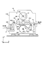
- FIG. 1 is a diagram showing an overall configuration of a projection exposure apparatus EX for a flexible substrate according to the present embodiment.
- the exposure apparatus EX irradiates the photosensitive layer of the flexible sheet-like substrate P conveyed from the process apparatus of the previous process with ultraviolet patterning light corresponding to the circuit pattern or wiring pattern for display. .
- Ultraviolet rays are, for example, g-line (436 nm), h-line (405 nm), i-line (365 nm) that are bright lines such as mercury discharge, or excimer lasers such as KrF, XeCl, ArF (wavelengths 248 nm, 308 nm, 193 nm, respectively)
- excimer lasers such as KrF, XeCl, ArF (wavelengths 248 nm, 308 nm, 193 nm, respectively)
- light having a wavelength of 400 nm or less from a semiconductor laser light source, an LED light source, a harmonic laser light source, or the like is included.
- the exposure apparatus EX of FIG. 1 is provided in the temperature control chamber EVC.
- the exposure apparatus EX is installed on the floor of a manufacturing plant via passive or active image stabilization units SU1, SU2.
- a transport mechanism for sending the substrate P sent from the previous process to the subsequent process at a predetermined speed is provided.
- the transport mechanism is a cylindrical position that is subjected to pattern exposure on the edge position controller EPC that controls the center of the substrate P in the Y direction (width direction perpendicular to the longitudinal direction) to a fixed position, the nipped drive roller DR4, and the substrate P.
- a rotating drum DR that rotates around a rotation center line AX2 and supports the substrate P while supporting it in a planar shape, tension adjusting rollers RT1 and RT2 that apply a predetermined tension to the substrate P wound around the rotating drum DR, and a substrate It is composed of two sets of drive rollers DR6, DR7 and the like for giving a predetermined slack (play) DL to P.
- a cylindrical cylindrical mask DM rotating around the rotation center line AX1, and an image of a part of a transmissive mask pattern formed on the outer peripheral surface of the cylindrical mask DM are transferred to the rotary drum DR.
- the alignment system AM includes an alignment microscope that detects an alignment mark or the like previously formed on the substrate P.
- the XY plane of the Cartesian coordinate system XYZ defined in FIG. 1 is set parallel to the factory floor, and the width direction (also referred to as the TD direction) of the surface of the substrate P coincides with the Y direction. Is set.
- the rotation center line AX1 of the cylindrical mask DM and the rotation center line AX2 of the rotary drum DR are both set parallel to the Y axis and are spaced apart in the Z axis direction.
- the projection optical systems PL1, PL2,... Of this embodiment are configured as a multi-lens system in which a plurality of projection fields (projected images) are arranged in a staggered manner, as will be described in detail later. Set to 1 ⁇ ( ⁇ 1).
- the diameter (radius from the center AX1) of the outer peripheral surface (pattern surface) of the cylindrical mask DM and the diameter (radius from the center AX2) of the outer peripheral surface (support surface) of the rotary drum DR can be made substantially equal. It can.
- the diameter of the cylindrical mask DM can be 30 cm
- the diameter of the rotary drum DR can be 30 cm. Note that the diameter (radius from the center AX1) of the outer peripheral surface (pattern surface) of the cylindrical mask DM and the diameter (radius from the center AX2) of the outer peripheral surface (support surface) of the rotary drum DR need to be the same. No, it can be very different.
- the diameter of the cylindrical mask DM may be set to 30 cm, and the diameter of the rotary drum DR may be set to about 40 to 50 cm.
- the said numerical value is an example and this invention is not limited to this.
- the thickness of the substrate P wound around the outer peripheral surface of the rotating drum DR is taken into consideration. For example, if the thickness of the substrate P is 100 ⁇ m (0.1 mm), the radius of the outer peripheral surface of the rotary drum DR is 0.1 mm smaller than the radius of the cylindrical mask DM (pattern surface).
- the diameter of the outer peripheral surface of the rotating drum DR is 100 / ⁇ cm depending on the circumferential ratio ⁇ . Therefore, it is necessary to process the diameter with an accuracy of several ⁇ m to submicron.
- illumination light for exposure corresponding to each visual field region of the projection optical systems PL1, PL2,.
- An illumination system IU that irradiates the pattern surface (outer peripheral surface) of the cylindrical mask DM is provided.
- the cylindrical mask DM is a reflection type
- the outer peripheral surface (reflection pattern surface) of the cylindrical mask DM is irradiated with exposure illumination light through some optical elements of the projection optical systems PL1, PL2,.
- a down-tilt illumination optical system for irradiating the light is provided.
- a mask pattern image formed on the outer peripheral surface of the cylindrical mask DM becomes a part of the outer peripheral surface of the rotating drum DR.
- the surface of the substrate P wound around (surface curved along the cylindrical surface) is continuously and repeatedly scanned and exposed.
- substrate P used by this embodiment is foil (foil) etc. which consist of metals or alloys, such as a resin film and stainless steel, for example.
- the material of the resin film is, for example, one of polyethylene resin, polypropylene resin, polyester resin, ethylene vinyl copolymer resin, polyvinyl chloride resin, cellulose resin, polyamide resin, polyimide resin, polycarbonate resin, polystyrene resin, and vinyl acetate resin. Or two or more.
- the substrate P can be selected so that its thermal expansion coefficient is not significantly large so that the amount of deformation caused by heat in various processing steps can be substantially ignored.
- a thermal expansion coefficient can be made small by mixing an inorganic filler with a resin film, for example.
- the inorganic filler for example, titanium oxide, zinc oxide, alumina, silicon oxide and the like are used.
- the substrate P may be a single layer of ultrathin glass having a thickness of, for example, about 100 ⁇ m manufactured by a float process or the like, and the above resin film, foil, or the like is bonded to the ultrathin glass.
- a laminated body may be sufficient.
- the said numerical value is an example and this invention is not limited to this.
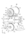
- FIG. 2 is a perspective view showing the arrangement relationship of the cylindrical mask DM, the plurality of projection optical systems PL1, PL2,..., And the rotating drum DR in the exposure apparatus EX shown in FIG.
- each of the projection optical systems PL1, PL2, PL3, PL4,... (Here, four projection optical systems are shown) provided between the cylindrical mask DM and the rotary drum DR is disclosed in, for example,
- the mask pattern is erected by connecting two catadioptric imaging lenses that use half of the circular projection field (half field) in tandem in the Z direction. Is projected on the substrate side at the same magnification as a non-inverted image of the above.
- the projection optical systems PL1, PL2, PL3, PL4... Have the same configuration, and details will be described later.
- the projection optical systems PL1, PL2, PL3, PL4,... are each attached to and integrated with a strong holding column PLM.
- the holding column PLM is made of a metal such as Invar having a small thermal expansion coefficient with respect to a temperature change, and can suppress a positional variation between the projection optical systems PL1, PL2, PL3, PL4,. it can.
- the rotation angle position (or position in the circumferential length direction) of the rotating drum DR is measured at both ends in the direction (Y direction) in which the rotation center line AX2 extends on the outer peripheral surface of the rotating drum DR.
- Scale portions GPa and GPb for the encoder system are respectively provided in an annular shape over the entire circumferential direction.
- the scale portions GPa and GPb are diffraction gratings in which concave or convex lattice lines are formed at a constant pitch (for example, 20 ⁇ m) in the circumferential direction of the outer peripheral surface of the rotary drum DR, and are configured as incremental scales.
- the said numerical value is an example and this invention is not limited to this.
- the substrate P is configured to be wound inside avoiding the scale portions GPa and GPb at both ends of the rotary drum DR.
- the outer peripheral surfaces of the scale portions GPa and GPb and the outer peripheral surface of the portion of the substrate P wound around the rotary drum DR are set to be the same surface (same radius from the center line AX2).
- the outer peripheral surfaces of the scale parts GPa and GPb may be made higher by the thickness of the substrate P in the radial direction than the outer peripheral surface for winding the substrate of the rotary drum DR.
- shafts Sf2 coaxial with the center line AX2 are provided on both sides of the rotation drum DR.
- Rotational torque from a drive source (not shown) (motor, deceleration gear mechanism, etc.) is given to the shaft portion Sf2.
- each of the scale parts GPa and GPb at both ends of the rotary drum DR is opposed to each other and fixed to a column PLM for fixing the projection optical systems PL1, PL2, PL3, PL4,.
- Encoder heads EN1 and EN2 are provided.
- FIG. 2 only two encoder heads EN1 and EN2 facing the scale part GPa are shown, but similar encoder heads EN1 and EN2 are also arranged facing the scale part GPb.
- Each encoder head EN1, EN2 projects a measurement light beam toward the scale portions GPa, GPb, and photoelectrically detects the reflected light beam (diffracted light), thereby changing the position of the scale portions GPa, GPb in the circumferential direction.
- Detection signals for example, a two-phase signal having a phase difference of 90 degrees
- the detected signal is interpolated and digitally processed by a counter circuit (not shown), whereby the angular change of the rotating drum DR, that is, the circumferential position change of the outer peripheral surface can be measured with submicron resolution. .
- the encoder heads EN1 and EN2 are arranged on installation orientation lines Le1 and Le2.
- the installation azimuth lines Le1 and Le2 are set in a plane parallel to the XZ plane in FIG. 2 through the projection region of the measurement light beam on the scale part GPa (GPb), and the extension line is the rotation of the rotary drum DR. This is a virtual line determined to intersect the center line AX2.
- the installation azimuth line Le1 is determined to be parallel to the principal ray of the imaging light beam projected onto the substrate P from the odd-numbered projection optical systems PL1 and PL3.
- the installation orientation line Le2 is determined to be parallel to the principal ray of the imaging light beam projected onto the substrate P from the even-numbered projection optical systems PL2 and PL4.
- a shaft portion Sf1 is provided on both ends of the cylindrical mask DM so as to be coaxial with the rotation center line AX1, and the rotational torque from a drive source (not shown) (not shown) is transmitted through the shaft portion Sf1 to the cylindrical mask DM.
- the encoder measurement scale part GPM is provided annularly over the entire circumferential direction centered on the rotation center line AX1. It has been.
- the transmission type mask pattern formed on the outer peripheral surface of the cylindrical mask DM is arranged inside avoiding the scale portions GPM at both ends. When a strict arrangement relationship is required, the outer peripheral surface of the scale portion GPM and the outer peripheral surface of the pattern surface (cylindrical surface) of the cylindrical mask DM are set to be the same surface (same radius from the center line AX1). .
- the encoder head EN11 is arranged in the direction of each field of the even-numbered projection optical systems PL2, PL4,... As viewed from the rotation center line AX1.
- These encoder heads EN11 and EN12 are also attached to a holding column PLM for fixing the projection optical systems PL1, PL2, PL3, PL4,.
- the encoder heads EN11 and EN12 are arranged on the installation azimuth lines Le11 and Le12 as in the arrangement state of the encoder heads EN1 and EN2 on the rotary drum DR side.
- the installation azimuth lines Le11 and Le12 are set in a plane parallel to the XZ plane in FIG. 2 through an area on which the measurement light beam of the encoder head is projected on the scale part GPM of the cylindrical mask DM. Is defined so as to intersect the rotation center line AX1 of the cylindrical mask DM.
- the cylindrical mask DM it is possible to draw and form a scale or a lattice pattern to be engraved on the scale portion GPM on the outer peripheral surface of the cylindrical mask DM together with a mask pattern of a device (display panel circuit, etc.)
- the relative positional relationship between the mask pattern and the scale part GPM can be set strictly.
- the cylindrical mask DM is exemplified as a transmission type.
- the scale portion GPM (scale, grid, origin pattern, etc.) can be formed together with the mask pattern of the device. Is possible.
- the metal columnar material having the shaft portion Sf1 is processed with a high-precision lathe and polishing machine, so that the roundness and axial blurring (eccentricity) of the outer peripheral surface are extremely low. It can be kept small. Therefore, if the scale part GPM is also formed on the outer peripheral surface by the same process as that for forming the mask pattern, highly accurate encoder measurement can be performed.
- the outer peripheral surface of the scale portion GPM formed on the cylindrical mask DM is set to have substantially the same radius as the mask pattern surface, and the outer periphery of the scale portions GPa and GPb formed on the rotary drum DR.
- the surface was set to have substantially the same radius as the outer peripheral surface of the substrate P. Therefore, the encoder heads EN11 and EN12 detect the scale portion GPM at the same radial position as the mask pattern surface (illumination area by the illumination system IU) on the cylindrical mask DM, and the encoder heads EN1 and EN2 are wound around the rotary drum DR.
- the scale portions GPa and GPb can be detected at the same radial position as the projection region (imaging plane of the projection image) on the substrate P. Therefore, Abbe error caused by the difference between the measurement position and the processing position in the radial direction of the rotating system can be reduced.
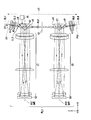
- the projection optical system PL1 shown in FIG. 3 includes a catadioptric-type telecentric first imaging optical system 51 and a second imaging optical system 58.
- the first imaging optical system 51 includes a plurality of lens elements, a focus correction optical member 44, an image shift correction optical member 45, a first deflection member 50, a first concave mirror 52 disposed on the pupil plane, and the like.
- the first imaging optical system 51 has a mask pattern that appears in the illumination area IR1 formed on the pattern surface (outer peripheral surface) of the cylindrical mask DM by the illumination light D1 (its principal ray is EL1) from the illumination system IU.
- the image is formed on an intermediate image plane on which the field stop 43 is disposed.
- the second imaging optical system 58 includes a plurality of lens elements, a second deflecting member 57, a second concave mirror 59 disposed on the pupil plane, a magnification correcting optical member 47, and the like.
- the second imaging optical system 58 converts an image limited by the aperture shape (for example, trapezoid) of the field stop 43 out of the intermediate image formed by the first imaging optical system 51 into the projection area PA1 of the substrate P. Re-image inside.
- the focus correction optical member 44 finely adjusts the focus state of a mask pattern image (hereinafter referred to as a projection image) formed on the substrate P, and the image shift correction optical member 45 projects.
- the image is slightly laterally shifted in the image plane, and the magnification correcting optical member 47 slightly corrects the magnification of the projected image within a range of about ⁇ tens of ppm.
- the first deflecting member 50 is slightly rotated around an axis parallel to the Z axis in FIG. 3, so that the projected image formed on the substrate P is slightly rotated in the image plane.
- a rotation correction mechanism 46 is provided.
- the imaging light beam EL2 from the pattern in the illumination area IR1 on the cylindrical mask DM is emitted from the illumination area IR1 in the normal direction, passes through the focus correction optical member 44 and the image shift correction optical member 45, and is subjected to the first deflection.
- a plane including both the rotation center line AX1 of the cylindrical mask DM and the rotation center line AX2 of the rotating drum DR shown in FIG. 2 (or FIG. 1) is defined as a center plane p3 (parallel to the YZ plane).
- the optical axis AX3 of the first imaging optical system 51 and the optical axis AX4 of the second imaging optical system 58 are both arranged so as to be orthogonal to the center plane p3.
- the illumination area IR1 when viewed in the XZ plane, the illumination area IR1 is biased by a predetermined amount in the ⁇ X direction with respect to the center plane p3, so that the extension of the principal ray EL1 of the illumination light D1 passing through the center in the illumination area IR1.
- the line is set so as to intersect the rotation center line AX1 of the cylindrical mask DM.
- the principal ray EL3 of the imaging light beam EL2 from the pattern located at the center point in the illumination area IR1 also advances in a state inclined in the XZ plane with respect to the center plane p3, and the first deflection member 50 1 reflection surface p4 is reached.
- the first deflection member 50 is a triangular prism that extends in the Y-axis direction.
- each of the first reflecting surface p4 and the second reflecting surface p5 includes a mirror surface (the surface of the reflecting film) formed on the surface of the triangular prism.
- the first deflecting member 50 is configured so that the principal ray EL3 from the illumination region IR1 to the first reflecting surface p4 is inclined with respect to the center plane p3 in the XZ plane and from the second reflecting surface p5 to the field stop 43.
- the imaging light beam EL2 is deflected so that the light beam EL3 is parallel to the center plane p3.
- a ridge line where the first reflecting surface p4 and the second reflecting surface p5 of the first deflecting member 50 intersect is disposed on the optical axis AX3.
- the first reflection surface p4 and the second reflection surface p5 are arranged at an asymmetric angle with respect to the plane p6.
- the angle ( ⁇ 1 + ⁇ 2) is set to be less than 90 °.
- the angle ⁇ 1 is set to less than 45 °
- the angle ⁇ 2 is set to substantially 45 °.
- the principal ray EL3 is the center of the first concave mirror 52, that is, the optical axis of the pupil plane. It can pass through the intersection with AX3, and a telecentric imaging state can be secured.
- the inclination angle in the XZ plane with respect to the center plane p3 of the principal ray EL3 between the illumination region IR1 and the first reflection plane p4 is ⁇ d
- the angle ⁇ 1 of the first reflection plane p4 is What is necessary is just to set like Formula (1).
- ⁇ 1 45 ° ⁇ ( ⁇ d / 2) (1)
- the imaging light beam EL2 passing through the first imaging optical system 51 and passing through the field stop 43 is a third reflecting surface (plane mirror) p8 of the second deflecting member 57 that is an element of the second imaging optical system 58. And passes through the plurality of lens elements to reach the second concave mirror 59 disposed on the pupil plane.
- the imaging light beam EL2 reflected by the second concave mirror 59 is again reflected by the fourth reflecting surface (planar mirror) p9 of the second deflecting member 57 through the plurality of lens elements, and passes through the magnification correcting optical member 47. It passes through and reaches the projection area PA1 on the substrate P. Thereby, the image of the pattern appearing in the illumination area IR1 is projected at the same magnification ( ⁇ 1) in the projection area PA1.
- the second deflection member 57 is also a triangular prism that extends in the Y-axis direction.
- each of the third reflecting surface p8 and the fourth reflecting surface p9 includes a mirror surface (the surface of the reflecting film) formed on the surface of the triangular prism.
- the second deflecting member 57 is arranged so that the principal ray EL3 between the field stop 43 and the third reflecting surface p8 is parallel to the central plane p3 in the XZ plane and between the fourth reflecting surface p9 and the projection area PA1.
- the image forming light beam EL2 is deflected so that the principal ray EL3 of the light beam tilts in the XZ plane with respect to the center plane p3.
- the projection area PA1 when viewed in the XZ plane, the projection area PA1 is also shifted by a predetermined amount in the ⁇ X direction with respect to the center plane p3. Therefore, the extension line of the principal ray EL3 of the imaging light beam reaching the projection area PA1. Is set so as to intersect the rotation center line AX2 of the rotary drum DR. As a result, the image plane formed in the projection area PA1 becomes a tangential plane of the surface (curved surface) of the substrate P supported by the outer peripheral surface of the rotary drum DR, and faithful projection exposure while maintaining resolution is possible.
- a ridge line where the third reflection surface p8 and the second reflection surface p9 of the second deflection member 57 intersect is arranged on the optical axis AX4, and the ridge line and the light
- the third reflection surface p8 and the fourth reflection surface p9 are arranged at an asymmetric angle with respect to the plane p7.
- the angle ( ⁇ 3 + ⁇ 4) is set to be less than 90 °, and the angle ⁇ 4 is 45 °.
- the angle ⁇ 3 is set to substantially 45 °.
- the odd-numbered projection optical systems PL3,... are configured in the same manner as in FIG. 3, and the even-numbered projection optical systems PL2, PL4,. Are arranged symmetrically with respect to the center plane p3. Further, in any of the odd-numbered and even-numbered projection optical systems PL1 to PL4..., The focus correction optical member 44, the image shift correction optical member 45, the rotation correction mechanism 46, and the magnification correction optical member 47 are imaged. It is provided as a characteristic adjustment mechanism.
- the projection condition of the projection image on the substrate P can be adjusted for each projection optical system.
- the projection conditions here include one or more items of the translation position, rotation position, magnification, and focus of the projection area on the substrate P.
- the projection condition can be determined for each position of the projection area with respect to the substrate P at the time of synchronous scanning. By adjusting the projection condition of the projection image, it is possible to correct the distortion of the projection image when compared with the mask pattern.
- the focus correcting optical member 44 is formed by superposing two wedge-shaped prisms in opposite directions (in the opposite direction with respect to the X direction in FIG. 3) to form a transparent parallel plate as a whole. This pair of prisms is slid in the direction of the slope without changing the distance between the opposing surfaces, and the thickness of the parallel plate is changed, so that the effective optical path length is finely adjusted and formed in the projection area PA1. The focus state of the pattern image is finely adjusted.
- the image shift correction optical member 45 is composed of a transparent parallel flat glass that can be tilted in the XZ plane in FIG. 3 and a transparent parallel flat glass that can be tilted in a direction perpendicular thereto. By adjusting the respective tilt amounts of the two parallel flat glass plates, the pattern image formed in the projection area PA1 can be slightly shifted in the X direction or the Y direction.
- the magnification correcting optical member 47 has a concave lens, a convex lens, and a concave lens arranged coaxially at predetermined intervals, the front and rear concave lenses are fixed, and the convex lens between them is moved in the direction of the optical axis (principal ray EL3). It is composed. As a result, the pattern image formed in the projection area PA1 is isotropically enlarged or reduced by a minute amount while maintaining a telecentric imaging state.
- the rotation correction mechanism 46 slightly rotates the first deflection member 50 around an axis parallel to the Z axis by an actuator (not shown).
- the rotation correction mechanism 46 can slightly rotate the pattern image formed in the projection area PA1 within the image plane.
- FIG. 4 is a diagram showing the arrangement of the illumination area IR and the projection area PA in the present embodiment.
- the projection optical system PL as the projection optical system PL, three odd-numbered projection optical systems PL1, PL3, PL5 and three even-numbered projection optical systems PL2, PL4, PL6 are arranged in the Y direction. To do.
- the left figure in FIG. 4 is a plan view of the six illumination regions IR1 to IR6 set on the cylindrical mask DM for each of the six projection optical systems PL1 to PL6 as viewed from the ⁇ Z side.
- FIG. 4 is a plan view of six projection areas PA1 to PA6 on the substrate P supported by the rotary drum DR, as viewed from the + Z side, for each of the six projection optical systems PL1 to PL6.
- a symbol Xs in FIG. 4 indicates the moving direction (rotating direction) of the cylindrical mask DM or the rotating drum DR.
- the illumination system IU individually illuminates the six illumination areas IR1 to IR6 on the cylindrical mask DM.
- each of the illumination areas IR1 to IR6 will be described as a trapezoidal area elongated in the Y direction.
- each of the illumination regions IR1 to IR6 may be a rectangular region including the trapezoid region.
- the odd-numbered illumination areas IR1, IR3, and IR5 have the same shape (trapezoid or rectangle), and are arranged at regular intervals in the Y-axis direction.
- Even-numbered illumination areas IR2, IR4, and IR6 are also arranged at regular intervals in the Y-axis direction.
- the even-numbered illumination areas IR2, IR4, IR6 have a trapezoidal (or rectangular) shape symmetrical to the odd-numbered illumination areas IR1, IR3, IR5 with respect to the center plane p3. Further, as shown in FIG. 4, each of the six illumination regions IR1 to IR6 is arranged so that the peripheral portions of adjacent illumination regions partially overlap in the Y direction.
- the outer peripheral surface of the cylindrical mask DM has a pattern formation region A3 where a pattern is formed and a pattern non-formation region A4 where a pattern is not formed.
- the pattern non-formation region A4 is arranged so as to surround the pattern formation region A3 in a frame shape, and particularly has a characteristic of shielding the illumination light beam that irradiates each of the illumination regions IR1 to IR6.
- the pattern formation region A3 moves in the direction Xs as the cylindrical mask DM rotates, and each partial region in the Y-axis direction of the pattern formation region A3 passes through one of the six illumination regions IR1 to IR6.
- the six illumination regions IR1 to IR6 are arranged so as to cover the entire width of the pattern formation region A3 in the Y-axis direction.
- each of the projection optical systems PL1 to PL6 displays a partial pattern image of the mask pattern appearing in the corresponding illumination areas IR1 to IR6 as six projections on the substrate P as shown in the right diagram in FIG. Projecting into areas PA1 to PA6.
- the pattern images in the odd-numbered illumination areas IR1, IR3, and IR5 are respectively projected onto the odd-numbered projection areas PA1, PA3, and PA5 arranged in a line in the Y-axis direction.
- the pattern images in the even-numbered illumination areas IR2, IR4, and IR6 are also projected onto the even-numbered projection areas PA2, PA4, and PA6 arranged in a line in the Y-axis direction.
- the odd-numbered projection areas PA1, PA3, PA5 and the even-numbered projection areas PA2, PA4, PA6 are arranged symmetrically with respect to the center plane p3.
- Each of the six projection areas PA1 to PA6 is arranged so that ends (trapezoidal triangular portions) of adjacent projection areas overlap each other in a direction (Y direction) parallel to the rotation center line AX2. Therefore, the exposure area A7 of the substrate P exposed in the six projection areas PA1 to PA6 with the rotation of the rotary drum DR has substantially the same exposure amount everywhere.
- the exposure apparatus EX detects an alignment mark formed on the substrate P or a reference mark or reference pattern formed on the rotary drum DR.
- An alignment system AM is provided for aligning the substrate P and the mask pattern and calibrating the base line and the projection optical system. The alignment system AM will be described below with reference to FIGS.
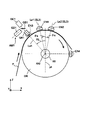
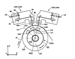
- FIG. 5 is a view of the arrangement of the rotary drum DR, the encoder heads EN1, EN2, and the alignment system AM1, as viewed in the XZ plane.
- FIG. 6 is a view of the arrangement of the rotary drum DR, the six projection areas PA1 to PA6 set on the substrate P, and the five alignment systems AM1 to AM5 in the XY plane.
- the installation azimuth lines Le1 and Le2 in which the encoder heads EN1 and EN2 are arranged are symmetrically inclined with respect to the center plane p3 including the rotation center line AX2 and parallel to the YZ plane. Is set.
- the inclination angles of the installation orientation lines Le1 and Le2 with respect to the center plane p3 are the projection areas PA1 described in FIG. 3 (or the odd-numbered projection areas PA1, PA3, PA5 and the even-numbered projection areas PA2, PA4, PA6) is set to be equal to the inclination angle ⁇ s from the central plane p3 of the principal ray EL3 reaching the center of PA6).
- an alignment system AM1 includes an illumination unit GC1 for irradiating a mark or pattern on the substrate P or the rotary drum DR with alignment illumination light, and a beam splitter GB1 for guiding the illumination light to the substrate P or the rotary drum DR.
- the image of the mark or pattern received through the objective lens system GA1, the objective lens system GA1 and the beam splitter GB1 that projects the illumination light onto the substrate P or the rotating drum DR and receives the light generated by the mark or pattern are configured by an imaging system GD1 that captures a two-dimensional CCD, CMOS, or the like.
- the illumination light for alignment from the illumination unit GC1 is light in a wavelength region that has little sensitivity to the photosensitive layer on the substrate P, for example, light having a wavelength of about 500 to 800 nm.
- the observation area (imaging area) of the mark or pattern by the alignment system AM1 is set to a range of about 200 ⁇ m square on the substrate P and the rotating drum DR, for example.
- the optical axis of the alignment system AM1 that is, the optical axis of the objective lens system GA1 is set in the same direction as the installation orientation line La1 extending from the rotation center line AX1 in the radial direction of the rotary drum DR.
- the installation orientation line La1 is inclined by an angle ⁇ j from the center plane p3, and is set so that ⁇ j> ⁇ s with respect to the inclination angle ⁇ s of the principal ray EL3 of the odd-numbered projection optical systems PL1, PL3, and PL5.
- an encoder head EN3 similar to the encoder heads EN1 and EN2 is provided on the installation direction line La1 at a position facing each of the scale portions GPa and GPb of the rotary drum DR.
- the rotational angle position (or circumferential position) of the rotating drum DR at the moment when the alignment system AM1 samples a mark or pattern image within the observation area (imaging area) can be accurately measured.
- an encoder head EN4 that faces each of the scale portions GPa and GPb of the rotary drum DR is also provided in the X-axis direction orthogonal to the center plane p3.
- FIG. 6 five alignment systems AM having the same configuration as the alignment system AM1 in FIG. 5 are provided.
- the objective lens systems GA1 to GA5 of the five alignment systems AM1 to AM5 are shown for easy understanding.
- the observation area (imaging area) Vw on the substrate P (or the outer peripheral surface of the rotating drum DR) by the objective lens systems GA1 to GA5 is parallel to the Y axis (rotation center line AX2) as shown in FIG. Arranged at predetermined intervals.
- the optical axes of the objective lens systems GA1 to GA5 passing through the center of each observation area (imaging area) Vw are all arranged in parallel to the XZ plane.
- the scale parts GPa and GPb are provided on both ends of the rotary drum DR, and a narrow band regulation band CLa by a concave groove or a convex rim is provided on the inside thereof.
- CLb is engraved over the entire circumference.
- the width in the Y direction of the substrate P is set to be smaller than the interval in the Y direction between the two regulation bands CLa and CLb.
- the substrate P is supported in close contact with the inner region sandwiched between the regulation bands CLa and CLb on the outer peripheral surface of the rotary drum DR.
- the exposure area A7 exposed by each of the six projection areas PA1 to PA6 is arranged at a predetermined interval in the X direction.
- a pattern may already be formed in each exposure area A7 of the substrate P, and a new pattern may be superimposed and exposed on the pattern.
- a plurality of marks (alignment marks) Ks1 to Ks5 for alignment are formed in a cross shape, for example.
- the mark Ks1 is provided in the peripheral area on the ⁇ Y side of the exposure area A7 at a constant interval in the X direction, and the mark Ks5 is fixed in the peripheral area on the + Y side of the exposure area A7 in the X direction. Provided at intervals.
- the marks Ks2, Ks3, and Ks4 are provided in a blank area between two adjacent exposure areas A7 in the X direction and in a line at intervals in the Y direction.
- the mark Ks1 is set so as to be sequentially captured while the substrate P is being sent within the imaging region Vw of the objective lens system GA1 (alignment system AM1).
- the mark Ks5 is set so as to be sequentially captured while the substrate P is being sent within the imaging region Vw of the objective lens system GA5 (alignment system AM5).
- the marks Ks2, Ks3, and Ks4 are captured in the imaging regions Vw of the objective lens system GA2 (alignment system AM2), the objective lens system GA3 (alignment system AM3), and the objective lens system GA4 (alignment system AM4), respectively.
- the position in the Y direction is determined.
- the imaging area Vw of each alignment system AM1 to AM5 is compatible.
- the imaging data is sampled at the timing when the marks Ks1 to Ks5 to be entered, and the angular position (circumferential position) of the rotating drum DR at that time is read from the encoder head EN3 and stored.
- the amount of deviation in the XY direction of each of the marks Ks1 to Ks5 with respect to each image area Vw is obtained.
- the determined marks Ks1 Based on the amount of deviation in the XY directions of Ks5 and the angular position (circumferential position) of the rotary drum DR read and stored by the encoder head EN3, the exposure area A7 on the substrate P and the projection areas PA1 to PA6 Can be accurately estimated from the measured values of the two encoder heads EN1 and EN2 arranged at the exposure position.
- the mask pattern is exposed to the exposure area of the substrate P. Accurate overlay exposure can be performed on A7.
- the substrate P may be as thin as about 100 ⁇ m, and a transparent film such as ITO may be formed as a base layer.
- a transparent film such as ITO
- the reflectance of the outer peripheral surface of the rotary drum DR that supports the substrate P is relatively high, or if there are many small scratches on the surface of several microns, exposure light for exposure is used. Is reflected, scattered, or diffracted by the outer peripheral surface of the rotating drum DR, and returns from the back surface side to the front side of the substrate P, giving the photosensitive layer exposure that causes noise that is not in the original mask pattern. .
- the outer peripheral surface of the rotating drum DR that is in contact with the exposure area A7 on the substrate P has a locally flat surface with a submicron flatness, and the reflectance is uniformly low.
- the reflectance can be, for example, 50, 45, 40, 35, 30, 25, 20, 15, 10, or 5% or less, preferably 20% or less, with respect to the illumination light for exposure.
- the said numerical value is an example and this invention is not limited to this.
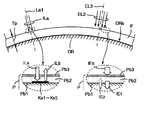
- FIG. 7 shows the configuration of the substrate P supported in close contact with the outer peripheral surface of the rotary drum DR, the reflection of the imaging light beam EL2 for exposure (illumination light IE0), and the alignment illumination light ILa.
- FIG. 8 is a diagram showing a cross-sectional structure of the outer peripheral surface of the rotary drum DR.
- the imaging light beam EL2 (illumination light IE0) traveling along the principal ray EL3 is projected onto the photosensitive layer Pb3 formed on the surface of the substrate P having a thickness Tp.
- the base layer Pb2 of the light sensitive layer Pb3 is made of a material having high light transmission properties such as ITO, the illumination light IE1 transmitted through the base layer Pb2 is hardly attenuated with respect to the original illumination light IE0.
- the base material Pb1 of the substrate P is a transparent resin film such as PET or PEN and the thickness is as thin as 100 ⁇ m or less
- the wavelength range of the illumination light IE0 (IE1) is 350 nm or more
- the base material Pb1 is The illumination light IE1 has a relatively large transmittance (80% or more). Therefore, the illumination light IE1 that has passed through the base material Pb1 reaches the outer peripheral surface DRs of the rotary drum DR.
- the illumination light IE1 transmitted through the base material Pb1 generates reflected light (including scattered light and diffracted light) IE2 from the outer peripheral surface DRs, and the base material Pb1 and the underlayer It returns to the photosensitive layer Pb3 in the order of Pb2. Since the reflected light IE2 is not the original patterning light beam EL2 for patterning, it becomes noise and gives unnecessary exposure to the photosensitive layer Pb3.
- One of the noises is, for example, a defocused image of a pattern image created by the imaging light beam EL2.
- the resolution (R) and the depth of focus (DOF) are generally determined by the wavelength ⁇ of the illumination light for exposure and the numerical aperture NA.
- the depth of focus (DOF) is It becomes about 70 ⁇ m.
- the imaging light beam EL2 is projected in a slightly defocused state on the outer peripheral surface DRs of the rotary drum DR, and the reflected light IE2 reflected by the outer peripheral surface DRs is On the surface of the photosensitive layer Pb3, the image light beam is further defocused. Therefore, a blurred image of the pattern image itself is projected on the photosensitive layer Pb3 together with the pattern image by the focused light beam EL2 in focus. That is, there may be a problem that an undesirable unnecessary pattern image (such as a blurred image) is reflected in the photosensitive layer Pb3.
- an undesirable unnecessary pattern image such as a blurred image
- a highly reflective substance such as aluminum (Al) is used.
- Al aluminum
- the illumination light ILa that has passed through the transparent region around the marks Ks1 to Ks5 reaches the outer peripheral surface DRs of the rotary drum DR, and the light reflected here is the mark Ks1. Since the images are picked up by the image sensor together with the reflected light ILb from .about.Ks5, the image contrast of the marks Ks1 to Ks5 may be lowered.
- the outer peripheral surface DRs of the rotary drum DR in the present embodiment is about 50, 45, 40, 35, 30, 25, 20, 15, 10, or 5% or less with respect to the illumination light IE0 for exposure. It is formed so as to have a reflectance. Therefore, in the rotating drum DR of the present embodiment, a base layer DR2 (thickness) made of chromium (Cr) or copper (Cu) is formed on the surface of a cylindrical base material DR1 made of iron (SUS) or aluminum (Al). Plating Td2).
- the surface of the underlying layer DR2 is optically polished to reduce the local surface roughness sufficiently, and then a top layer DR3 (thickness Td3) made of chromium oxide (Cr2O3) or diamond-like carbon (DLC) is formed thereon.
- a top layer DR3 thinness Td3 made of chromium oxide (Cr2O3) or diamond-like carbon (DLC) is formed thereon.
- the thickness Td2 of the underlayer DR2 can be arbitrarily set in the range of several hundred nm to several ⁇ m, but the thickness Td3 of the top layer DR3 has a certain range of conditions in order to adjust the reflectance of the outer peripheral surface DRs.
- the base layer DR2 is made of chromium (Cr) and the top layer DR3 is made of chromium oxide (Cr2O3), the wavelength characteristic (spectral reflectance) of the reflectance of the outer peripheral surface DRs using the thickness Td3 of the top layer DR3 as a parameter. Will be described with reference to FIG.
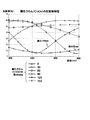
- FIG. 9 is a graph of simulation results when the refractive index n of chromium oxide is 2.2 and the absorption coefficient k is 0.
- the vertical axis is the reflectance (%) of the outer peripheral surface DRs, and the horizontal axis is the wavelength (nm). ).
- FIG. 9 shows the characteristics of six spectral reflectances obtained by changing the thickness Td3 of the top layer DR3 of chromium oxide by 30 nm between 0 and 150 nm.
- the reflectance can be 20% or less (15% or less in the simulation) over the entire wavelength band of 350 nm to 500 nm.
- the wavelength of the illumination light ILa for alignment is about 500 nm with a reflectance of about 7% with respect to the wavelength of 436 nm (g-line exposure light)
- the reflectance is also about 12%.
- the wavelength of the exposure light is 405 nm (such as a semiconductor laser for Blu-ray near the h line)
- the thickness Td3 of the top layer DR3 of chromium oxide is set to about 120 nm.
- a reflectance of about 40% can be achieved for the illumination light ILa for alignment near 500 nm while having a minimum value.
- the reflectance for exposure light (illumination light IE0) having a wavelength band of 350 to 436 nm increases to about 50%, and the wavelength of 500 nm
- the reflectance with respect to the alignment illumination light ILa is 40% or less.
- the thickness Td3 of the top layer DR3 of chromium oxide is set to about 90 nm, the reflectance of the outer peripheral surface DRs can be reduced to 30% or less for ultraviolet light in a wavelength band shorter than the wavelength of 350 nm, and the wavelength of 500 nm.
- the reflectance of the outer peripheral surface DRs with respect to the alignment illumination light ILa can be increased to about 60%.
- the reflectance of the outer peripheral surface DRs with respect to the alignment illumination light and the exposure illumination light is about several to 50%.
- the top layer DR3 made of chromium oxide is used.
- the simulation of FIG. 9 is an example in which a chromium layer is formed on the base material DR1 of the rotating drum DR, and a chromium oxide layer is formed on the substrate DR1 with a controlled thickness to adjust the reflectance.
- the material of the base layer DR2 may be aluminum (Al), copper (Cu), silver (Ag), gold (Au), etc. in addition to chromium (Cr).
- the above-mentioned chromium oxide, a dielectric having a high refractive index capable of relatively controlling reflectance, titanium oxide (TiO), zircon, hafnium oxide, diamond-like carbon (DLC) And metal compounds such as oxides and nitrides can be used in the same manner.
- the illumination light for exposure (IE0) is ultraviolet light having a wavelength of 436 nm (g-line) or less
- the illumination light for alignment (ILa) is in a visible range where the photosensitive layer (Pb3) is not exposed.
- the base layer DR2 is formed of a metal material such as copper (Cu) that has a low reflectance with respect to light in the ultraviolet region and a high reflectance with respect to light in the red wavelength region. It is also possible to make a difference in the reflectance with respect to each of the illumination light for alignment (ILa) and the illumination light for exposure (IE0).
- DLC diamond-like carbon
- the exposure apparatus according to the first embodiment is a so-called multi-lens system
- the mask pattern image formed in each of the projection areas PA1 to PA6 of the plurality of projection optical systems PL1 to PL6 results in the Y direction (or as a result). It is necessary to be well spliced in the (X direction) and to be well aligned (superposed) with the underlying pattern on the substrate P. For this purpose, calibration is required to keep the joint accuracy by the plurality of projection optical systems PL1 to PL6 within an allowable range.
- the relative positional relationship of the projection optical systems PL1 to PL6 with respect to the projection areas PA1 to PA6 and the observation (imaging) area Vw of the alignment systems AM1 to AM5 needs to be precisely determined by baseline management. . Calibration is also required for the baseline management.
- At least a part of the outer peripheral surface of the rotary drum DR that supports the substrate P is used for calibration for confirming splicing accuracy by the plurality of projection optical systems PL1 to PL6 and calibration for baseline management of the alignment systems AM1 to AM5.
- a calibration reference mark or reference pattern is provided, and the reference mark or reference pattern is moved under the objective lens of the projection optical system or alignment system during calibration.
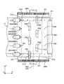
- FIG. 10 is a perspective view of the rotary drum DR that is integrally turned with the shaft portion Sf2 coaxial with the rotation center line AX2, and similarly to the configuration shown in FIGS. 2 and 6, the scale for encoder measurement is shown. Portions GPa and GPb and regulation bands CLa and CLb are provided. Further, in the present embodiment, a plurality of line patterns RL1 inclined at +45 degrees with respect to the Y axis and ⁇ 45 with respect to the Y axis are provided on the entire circumference sandwiched between the regulation bands CLa and CLb on the outer peripheral surface of the rotary drum DR. A mesh-like reference pattern (which can also be used as a reference mark) RMP is provided in which a plurality of line patterns RL2 inclined at degrees are repeatedly engraved at a constant pitch (period) Pf1, Pf2.
- the reference pattern RMP is the outer peripheral surface of the substrate P and the rotating drum DR.
- a uniform oblique pattern oblique lattice pattern
- the line patterns RL1 and RL2 do not necessarily need to be inclined at 45 degrees, and may be a vertical and horizontal mesh pattern in which the line pattern RL1 is parallel to the Y axis and the line pattern RL2 is parallel to the X axis. Furthermore, the line patterns RL1 and RL2 do not need to intersect at 90 degrees, and the rectangular area surrounded by the two adjacent line patterns RL1 and the two adjacent line patterns RL2 is other than a square (or a rectangle). The line patterns RL1 and RL2 may be crossed at such an angle as to form a rhombus.
- the pitches Pf1 and Pf2 of the line patterns RL1 and RL2 shown in FIG. 10 are the expected fluctuation amounts of the baseline of the alignment system (relative positional relationship between the projection area PA and the imaging area Vw of the projection optical system PL), Alternatively, in consideration of an expected fluctuation amount between the plurality of projection optical systems PL1 to PL6 of the multi-lens method, it is sufficient that the expected fluctuation amount is at least twice or more. For example, when the maximum value of the expected fluctuation amount is 10 ⁇ m, the pitches Pf1 and Pf2 vary depending on the line width LW (5 to 20 ⁇ m) of the line patterns RL1 and RL2, but if it is about 30 to 50 ⁇ m, Accurate calibration is possible.
- the line width LW of each of the line patterns RL1 and RL2 is determined by the precision (resolution) of the drawing apparatus for engraving each of the line patterns RL1 and RL2, the limit that can be reduced by the etching conditions, etc., but the alignment systems AM1 to AM5 can stabilize the image. It is better to make it as thin as possible within the range that can be analyzed.
- the pitches Pf1 and Pf2 of the line patterns RL1 and RL2 are set to about 50 ⁇ m.
- intersections of the line patterns RL1 and RL2 appear at a pitch of about 70 ⁇ m in the Y direction and the X direction, and if the imaging (observation) region Vw is in the range of 200 ⁇ m square, a specific one intersection is improved. Capturing and image analysis of misalignment can be performed.
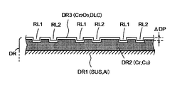
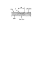
- FIG. 11 is a cross-sectional view in which a part of the reference pattern RMP by the line patterns RL1 and RL2 is broken along the X axis shown in the circle in FIG.
- a chromium or copper underlayer DR2 is deposited thickly by plating on the surface of a cylindrical base material DR1 of iron or aluminum.
- the surface of the underlayer DR2 is optically polished to improve the flatness, and then a photoresist is applied to the entire periphery of the underlayer DR2, and a reference pattern RMP based on the line patterns RL1 and RL2 is applied to the underlayer DR2 by a drawing apparatus.
- the relative positional relationship (especially the positional relationship in the circumferential direction) between the reference pattern RMP and the scale portions GPa and GPb can be made constant by drawing the grid lines of the scale portions GPa and GPb together. .
- the resist corresponding to the line patterns RL1 and RL2 is removed, and the exposed underlayer DR2 (chrome or copper) is etched to a predetermined depth, and then the top layer DR3 is formed on the surface.
- chrome or copper chrome or copper
- the top layer DR3 is formed on the surface.
- Chromium oxide or DLC Chromium oxide or DLC
- the thickness of the top layer DR3 is set based on the characteristics shown in FIG.
- the step amount ⁇ DP of the line patterns RL1 and RL2 (concave portions) by the finally formed top layer DR3 is compared with the design value by measurement, and is confirmed to be within a predetermined allowable range.
- the reference pattern RMP based on such line patterns RL1 and RL2 can suppress the reflectance of the surface to the illumination light for exposure to 20% or less as in the first embodiment. For this reason, even if the illumination light for exposure is reflected by the reference pattern RMP, the energy is not high enough to be exposed as an unnecessary pattern on the photosensitive layer Pb3, so that there is substantially no problem.
- the line patterns RL1 and RL2 are formed as concave portions by etching as shown in FIG. 11, the line patterns RL1 and RL2 may be formed as convex portions using a negative photoresist.
- the step amount ⁇ DP shown in FIG. 11 may be set under the following conditions.
- the center wavelength of the illumination light IE0 for exposure is ⁇ 1
- the center wavelength of the illumination light ILa for alignment is ⁇ 2
- the central wavelength ⁇ 1 of the illumination light IE0 for exposure ⁇ 1 ⁇ (m + 1/8) / 2 ⁇ ⁇ DP ⁇ ⁇ 1 ⁇ (m + 7/8) / 2 (3)
- the step amount ⁇ DP may be set.
- the step amount ⁇ DP can be set.
- the range of the step amount ⁇ DP can be determined by replacing the wavelength ⁇ 1 in the above formulas (3) and (4) with ⁇ 2.
- the range of the step amount ⁇ DP required for the wavelength ⁇ 1 of the illumination light for exposure is compared with the range of the step amount ⁇ DP required for the wavelength ⁇ 2 of the illumination light for alignment, and the two ranges overlap or are close to each other.
- the intensity of the reflected light generated from the reference pattern RMP can be reduced for both the illumination light for exposure and the illumination light for alignment. That is, a step amount ⁇ DP that satisfies or approximates the above equations (3) and (4) is set for both the center wavelength ⁇ 1 of the exposure illumination light and the center wavelength ⁇ 2 of the alignment illumination light. It ’s fine.
- the reflectance is adjusted by laminating the relatively thick base layer DR2 and the top layer DR3 on the outer peripheral surface of the cylindrical base material DR1 serving as the rotary drum DR.
- a stacked structure having a larger number of layers may be used.
- the base material DR1 is cut out from an Al (aluminum) block, and the outer peripheral surface of the base material DR1 is compared for flatness (roundness and surface roughness) processing. After plating hard chromium (Cr) thickly, it is further plated with copper (Cu) as the underlying layer DR2 shown in FIGS.
- the DLC may be laminated with a predetermined thickness.
- the reference pattern RMP line patterns RL1, RL2
- the lattice lines of the scale portions GPa, GPb are engraved on the hard chromium layer or the copper base layer DR2 thereon.
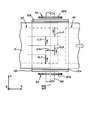
- FIG. 12 is a front view of the main part of the exposure apparatus (pattern drawing apparatus) according to the present embodiment as viewed in the XZ plane
- FIG. 13 is a top view of the configuration of FIG. 12 as viewed in the XY plane.
- Pattern drawing is performed by linear scanning lines LL1, LL2, LL3, and LL4 of spot light (for example, 4 ⁇ m diameter). Since each of the scanning lines LL1 to LL4 has a relatively short scanning length in the Y direction, the scanning lines LL1 to LL4 are staggered symmetrically with respect to the center plane p3.
- the odd-numbered scanning lines LL1 and LL3 are arranged on the ⁇ X side with respect to the central plane p3, and the even-numbered scanning lines LL2 and LL4 are arranged with respect to the central plane p3.
- this avoids spatial interference between the odd-numbered drawing modules UW1 and UW3 that scan the spot light along the scanning lines LL1 to LL4 and the even-numbered drawing modules UW2 and UW4. This is because they are arranged symmetrically with respect to the center plane p3.
- a scale disk SD for encoder measurement is individually attached to the shaft portion Sf2 of the rotary drum DR.
- the scale part GPa (and GPb) engraved on the outer peripheral surface of the scale disk SD is measured by the encoder head EN1 arranged on the installation direction line Le1 and the encoder head EN2 arranged on the installation direction line Le2.
- an encoder head EN3 that reads the scale portion GPa (and GPb) is also arranged at the position of the installation direction line La1 where the alignment systems AM1 to AM5 are arranged as shown in FIGS.
- the drawing module UW1 receives a beam LB from an external ultraviolet laser light source (continuous or pulsed) and switches the projection / non-projection of the beam LB onto the substrate P at high speeds
- AOM (Acousto-Optic Modulator) 80, AOM 80 are provided with a rotating polygon mirror 82, a bending mirror 84, an f- ⁇ lens system 86, a photoelectric element 88, and the like for scanning the beam LB from the scanning line LL1 on the substrate P.
- the beam BS1 projected onto the substrate P through the f- ⁇ lens system 86 is modulated by the AOM 80 that is turned on / off based on the CAD information of the pattern to be drawn during scanning in the Y direction, and the light sensitivity of the substrate P Draw a pattern on the layer.
- the AOM 80 By synchronizing the scanning in the Y direction of the beam BS1 along the scanning line LL1 and the movement of the substrate P in the X direction by the rotation of the rotating drum DR, a pattern is exposed at a portion corresponding to the scanning line LL1 in the exposure area A7. Is done. Because of such a drawing method, as shown in FIG.
- the axis of the beam BS1 reaching the substrate P is in a direction coinciding with the installation orientation line Le1 when viewed in the XZ plane.
- the accuracy of the joint between the scanning lines LL1 to LL4 is important.
- the exposure area A7 first, exposure of the areas corresponding to the odd-numbered scanning lines LL1 and LL3 is started, and from the position where the substrate P has advanced in the circumferential direction by the distance ⁇ Xu, Exposure of an area corresponding to the even-numbered scanning lines LL2 and LL4 is started. Therefore, by accurately setting the drawing start point and the drawing end point by the spot light of each of the scanning lines LL1 to LL4, the pattern formed in the entire exposure area A7 can be satisfactorily pinched.
- the rotary drum DR having the structure shown in FIG. 8 of the first embodiment or the rotary drum DR having the structure shown in FIGS. 10 and 11 of the second embodiment is used. By using it, the reflection of an unnecessary pattern which becomes noise is reduced, and highly accurate patterning is achieved.
- the substrate P in addition to the cylindrical rotary drum DR, the substrate P has a flat support surface, and is curved in a cylindrical shape with a large curvature in the transport direction of the substrate P. It may have a support surface.
- the invention can be similarly applied even to a support device in which a gas layer is formed by an air bearing on the support surface of these support devices and the substrate is supported by floating a small amount of the substrate by the gas layer. .
- Cu copper
- Cr chromium
- Cr 2 O 3 trivalent chromium oxide
- the base layer DR2 to be formed on the base material DR1 may be Cu
- CrO may be formed by plating, vapor deposition, or sputtering as the top layer DR3 to be deposited on the base layer DR2. good.
- the diamond-like carbon (DLC) formed as the top layer DR3 of each of the previous embodiments is composed of carbon atoms, and has an amorphous structure and / or an amorphous structure containing a crystalline material.
- the sp2 bond of graphite and the sp3 bond of diamond are mixed.
- DLC is formed as a hard film, but its properties are distinguished depending on the amount of hydrogen content and whether the crystalline electron orbit contained is closer to diamond or graphite.
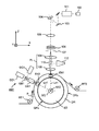
- FIG. 14 is a perspective view showing a modified example of the reference pattern RMP formed on the outer peripheral surface DRs of the rotating drum DR as a fourth embodiment. The same members as those of the rotating drum DR in FIG. Is attached.
- a scale disk SD for encoder measurement is fastened by a plurality of screws FB on both end faces in the direction (Y-axis direction) in which the shaft portion Sf2 of the rotary drum DR extends, as in FIGS. Has been.
- the diameters (or the radius from the center line AX2) of the scale portions GPa and GPb formed on the outer peripheral surface of the scale disk SD are the diameters of the outer peripheral surface DRs (or the radius from the center line AX2) of the rotary drum DR. ).
- the outer peripheral surface DRs of the rotary drum DR has a line pattern RLa extending linearly along a direction (Y-axis direction) parallel to the rotation center line AX2 and linearly extending along the circumferential direction (parallel to the XZ plane).
- Two line patterns RLb and RLc that circulate in the plane are formed as the reference pattern RMP.
- the line patterns RLa are arranged at 45 ° intervals in the circumferential direction.
- the two line patterns RLb and RLc are arranged at a certain interval in a direction parallel to the rotation center line AX2 (Y-axis direction).
- the angular interval ⁇ in the circumferential direction of the line pattern RLa is not limited to 45 °, and may be any number of times.
- the constant interval corresponds to the interval in the Y-axis direction of each imaging region Vw of the alignment systems AM1 to AM5 shown in FIG. That is, the line patterns RLa and the two line patterns RLb and RLc intersect each other so that the intersection ALA appears one after another in each imaging area Vw of the alignment systems AM1 to AM5 as the rotary drum DR rotates. RLa, RLb, and RLc are arranged, and the line pattern portion of the intersection ALA is detected as the reference pattern RMP.
- the alignment systems AM1 to AM5 can detect the line patterns RLb and RLc together with the marks Ks1 to Ks5 within the imaging region Vw.
- the margin between the two exposure areas A7 arranged adjacent to each other in the feeding direction on the substrate P shown in FIG. 6 is set to a predetermined dimension or more.
- the crossing part ALA by line pattern RLa, RLb, RLc formed in the outer peripheral surface DRs of rotary drum DR can also be reliably arrange
- the circumferential distance LK of the line pattern RLa along the outer peripheral surface DRs uses the angular interval ⁇ in the circumferential direction of the line pattern RLa described above.
- LK ⁇ ⁇ Rdd ⁇ ( ⁇ / 360) (5)
- LU the size of the blank portion between the two exposure areas A7 in the longitudinal direction (feed direction) of the substrate P.
- a pattern RLa can be arranged.
- the reference pattern RMP is configured by the line patterns RLa, RLb, and RLc that linearly extend in the longitudinal direction (feed direction) and the short direction (Y-axis direction) of the substrate P.
- the two-dimensional position of the intersection ALA appearing in each imaging region Vw of the alignment systems AM1 to AM5 can be directly measured in the direction along the horizontal scanning line or the vertical scanning line of the imaging device, and the computation time of the image processing There is an advantage of being shortened.
- the line patterns RLa, RLb, and RLc are formed on the outer peripheral surface DRs of the rotary drum DR.
- the line patterns RLa, RLb, and RLc are formed as recesses having a line width LW, and the recesses are filled with a material PI that absorbs ultraviolet rays (exposure light).
- the material PI is a paint containing an ultraviolet absorber (cured after drying), absorbs scattered light and diffracted light generated at the step edge, and determines the amount of scattered light and diffracted light reaching the front side of the substrate P.
- an ultraviolet absorber cured after drying
- the UV absorber is commercially available from BASF-SE under the trade name Uvinul (registered trademark) or TINUVIN (registered trademark), and absorbs exposure light in the ultraviolet wavelength range, but for alignment in the visible wavelength range.
- the illumination light has a characteristic of hardly absorbing.
- the line pattern constituting the reference pattern RMP is formed by the concave portion, and the concave portion is filled with the ultraviolet absorbing material. Therefore, the outer peripheral surface DRs of the rotary drum DR is irradiated by exposure light. The stray light reflected from the light can be further reduced. Note that the method of filling the concave portion of the outer peripheral surface DRs with the ultraviolet absorbing material can be similarly applied to the line patterns RL1 and RL2 shown in FIGS. Moreover, the coating material containing such an ultraviolet absorber can also be used for repairing irregular portions such as scratches and dents on the outer peripheral surface DRs in contact with the substrate P.
- the substrate supporting apparatus is supported by the tension adjusting rollers TR1, TR2 and the shaft portion Sf2, and the rotating drum DR, the scale disk SD, the encoder heads EN1, EN3, which wind the substrate P, as in the previous embodiments.
- the alignment system AM1 (and AM2 to AM5) includes an objective lens system GA1, a beam splitter GB1, an illumination unit GC1, and an imaging system GD1.
- the exposure unit is an illumination that uniformly illuminates a light source 100 that generates exposure illumination light (exposure light) and a DMD (Digital Micromirror Device (registered trademark)) 104 in which a large number of movable micromirrors are two-dimensionally arranged with uniform illuminance.
- a light source 100 that generates exposure illumination light (exposure light)
- a DMD Digital Micromirror Device (registered trademark)) 104 in which a large number of movable micromirrors are two-dimensionally arranged with uniform illuminance.
- the lens system 105 that condenses the exposure light reflected by the micromirrors of the system 101, the mirror 103, and the DMD 104, the MLA (Micro-Lens Array) 106 in which a number of microlenses are two-dimensionally arranged, and the rotating drum DR Projection optical system composed of lens systems 108 and 109 for projecting the light spot formed in the aperture of the field stop 107 by the microlenses of the field stop 107 and the MLA 106 conjugate with the surface of the substrate P onto the substrate P PL.
- MLA Micro-Lens Array
- the pupil plane in the projection optical system PL of the present embodiment is provided with a beam splitter 110 that can be inserted and removed in a direction (Y-axis direction) orthogonal to the paper surface of FIG.
- this beam splitter 110 When this beam splitter 110 is inserted, the exposure light from the MLA 106 passes through the lens system 108, the beam splitter 110, and the lens system 109 of the projection optical system PL, or the outer peripheral surface DRs of the rotating drum DR.
- a part of the reflected light reflected and returned by the surface of the substrate P or the outer peripheral surface DRs when projected onto the substrate P can be guided to the monitor system 112 including a condensing lens, a photoelectric element, and the like.
- the monitor system 112 measures the amount of reflected light (exposure light) from the surface of the substrate P or the outer peripheral surface DRs, and determines whether or not an appropriate exposure amount (illuminance) is given to the substrate P. Alignment that collects light information (optical image, diffracted light, etc.) related to the reference patterns RMP on the marks Ks1 to Ks5 on the substrate P and the outer peripheral surface DRs based on the light amount monitor for performing or the reflected light (exposure light) Configured as a monitor.
- the pattern drawing data (CAD data), the information on the feeding position of the substrate P based on the measurement signal from the encoder head EN1 (or EN3), or the alignment system AM1 (AM2 to AM2).
- the angles of the micromirrors of the DMD 104 are switched at high speed.
- the exposure light reflected by each micromirror is switched between a state where it is incident on the microlens corresponding to the MLA 106 and a state where it is not incident, so that a pattern according to the drawing data is exposed (drawn) on the substrate P.
- the pattern exposure apparatus of this embodiment shown in FIG. 16 is also provided with a plurality of exposure units in the direction parallel to the rotation center line AX2 (Y-axis direction) under the conditions shown in FIGS.
- the aperture shape of the field stop 107 in FIG. 16 is a trapezoidal shape similar to the shape of each of the exposure areas PA1 to PA6 in FIG. 4, and a number of light spots created by the MLA 106 are formed in the trapezoidal aperture. Should be arranged at a constant pitch.
- the MLA 106 shown in FIG. 16 is formed so that the focus surface defined by the condensing points of a large number of light spots formed on the emission side of the MLA 107 is curved in a cylindrical shape like the outer peripheral surface DRs of the rotary drum DR.
- the focal lengths may be slightly different between the microlenses arranged in the X direction.
- DM cylindrical mask
- DR rotating drum
- DRs outer peripheral surface of rotating drum
- DR1 base material of rotating drum
- DR2 base layer of rotating drum
- DR3 rotating drum Top layer
- P flexible substrate
- PL1, PL2, PL3, PL4 projection optical system
- AM1-AM5 ... alignment system
- RMP ... reference pattern
- RL1, RL2, RLa, RLb, RLc Line pattern
- UW1 to UW4 Drawing module.
Landscapes
- Physics & Mathematics (AREA)
- General Physics & Mathematics (AREA)
- Engineering & Computer Science (AREA)
- Multimedia (AREA)
- Exposure And Positioning Against Photoresist Photosensitive Materials (AREA)
- Container, Conveyance, Adherence, Positioning, Of Wafer (AREA)
- Registering, Tensioning, Guiding Webs, And Rollers Therefor (AREA)
- Treatments Of Macromolecular Shaped Articles (AREA)
- Laminated Bodies (AREA)
Description
本願は、2012年8月28日に出願された特願2012-188116号に基づき優先権を主張し、その内容をここに援用する。
有機ELによるディスプレー製造において、より低コストで量産性の高い方式のひとつとして、可撓性(フレキシブル)の樹脂材やプラスチック、或いは金属箔を厚みが200μm以下の長尺状のシート(フィルム)として形成し、その上に、ディスプレーのバック・プレートやトップ・プレートを、ロール・ツー・ロール(Roll to Roll)方式で直接作り込むことが提案されている(特許文献1)。
さらに特許文献1では、絶縁層を挟んで上下に積層されるTFTのゲート電極層とドレイン/ソース電極層との相対的な位置関係や各電極の形状等を精密に仕上げる為に、紫外線の照射によって表面の親撥液性を改質する自己組織化単分子層(SAM)を形成し、紫外線によるパターン露光装置を使って、各電極層の形状を、より精密に仕上げる工夫が提案されている。
これに対して、ロール・ツー・ロール方式により、連続的に搬送される可撓性のシート基板にマスクのパターンを繰り返し露光する場合には、シート基板の搬送方向を走査方向とし、マスクを円筒状の回転マスクにした走査型露光装置にすることにより、生産性の飛躍的な向上が期待できる。
ITO等の透明層が形成された透明度の高いPETフィルム、PEN(Poly-Ethylene Naphthalate)フィルム、極薄ガラス等に、露光装置を用いてパターニングする場合、その基板の表面に塗布された光感応層(例えば、フォトレジスト、感光性シランカップリング材等)に投射されるパターン露光光は、基板の下のパッド面や回転ドラムの外周面にまで達する。
また、本発明の態様は、基板を支持する装置の支持面の一部に形成された基準マークや基準パターン、又は、基板に形成されたマークやパターンからの反射光(戻り光)を、アライメント顕微鏡等による光学的な観察装置によって良好に検出できる基板支持装置を提供することを目的とする。
さらに、本発明の態様は、そのような基板支持装置によって支持される基板に、高精度な光パターニングを施す露光装置を提供することを目的とする。
本発明の第3の態様によれば、精密なパターン露光が可能な露光装置を提供することができる。
図1は、本実施形態によるフレキシブル基板用の投影型露光装置EXの全体構成を示す図である。露光装置EXは、前工程のプロセス装置から搬送されてくる可撓性のシート状の基板Pの光感応層に対して、ディスプレー用の回路パターンや配線パターンに対応した紫外線のパターニング光を照射する。
紫外線は、例えば水銀放電等の輝線であるg線(436nm)、h線(405nm)、i線(365nm)、或いはKrF,XeCl、ArF等のエキシマレーザ(各々、波長248nm,308nm,193nm)、または、半導体レーザ光源、LED光源、高調波レーザ光源等からの波長400nm以下の光、を含む。
搬送機構は、基板PのY方向(長尺方向と直交した幅方向)の中心を一定位置に制御するエッジポジションコントローラEPC、ニップされた駆動ローラDR4、基板P上でパターン露光される部分を円筒面状に支持しつつ、回転中心線AX2の回りに回転して基板Pを搬送する回転ドラムDR、回転ドラムDRに巻き付く基板Pに所定のテンションを与えるテンション調整ローラRT1、RT2、及び、基板Pに所定のたるみ(あそび)DLを与える為の2組の駆動ローラDR6、DR7等で構成される。
アライメント系AMは、基板Pに予め形成されたアライメントマーク等を検出するアライメント顕微鏡を含む。
また、本実施形態の投影光学系PL1、PL2、・・・は、詳しくは後述するが、複数の投影視野(投影像)が千鳥配置になるようなマルチレンズ方式として構成され、その投影倍率は等倍(×1)に設定される。
なお、円筒マスクDMの外周面(パターン面)の直径(中心AX1からの半径)と、回転ドラムDRの外周面(支持面)の直径(中心AX2からの半径)は、必ずしも同じにしておく必要はなく、大きく異なっていても良い。例えば、円筒マスクDMの直径を30cmに、回転ドラムDRの直径を40~50cm程度にしても良い。
なお、上記数値は一例であって本発明はこれに限定されない。
尚、回転ドラムDRの直径を円筒マスクDM(パターン面)の直径と等しくする場合、厳密には、回転ドラムDRの外周面に巻き付けられる基板Pの厚みを考慮したものとなる。例えば、基板Pの厚みを100μm(0.1mm)とすると、回転ドラムDRの外周面の半径は、円筒マスクDM(パターン面)の半径に対して、0.1mmだけ小さなものとする。
さらに、回転ドラムDRの外周面の周方向の全長(周長)を、ちょうど良い長さ、例えば100.0cmにする場合は、回転ドラムDRの外周面の直径は円周率πによって100/πcmとなる為、直径を数μm~サブミクロンの精度で加工しておく必要がある。
尚、円筒マスクDMが反射型の場合は、露光用の照明光を投影光学系PL1、PL2、・・・の一部の光学素子を介して円筒マスクDMの外周面(反射型のパターン面)に向けて照射する落斜照明光学系が設けられる。
樹脂フィルムの材質は、例えば、ポリエチレン樹脂、ポリプロピレン樹脂、ポリエステル樹脂、エチレンビニル共重合体樹脂、ポリ塩化ビニル樹脂、セルロース樹脂、ポリアミド樹脂、ポリイミド樹脂、ポリカーボネート樹脂、ポリスチレン樹脂、酢酸ビニル樹脂のうち1又は2以上を含む。
また、基板Pは、フロート法等で製造された厚さが例えば100μm程度の極薄ガラスの単層体であってもよいし、この極薄ガラスに上記の樹脂フィルム、箔等を貼り合わせた積層体であってもよい。
なお、上記数値は一例であって本発明はこれに限定されない。
図2において、円筒マスクDMと回転ドラムDRとの間に設けられる投影光学系PL1、PL2、PL3、PL4、・・・(ここでは4つの投影光学系を図示)の各々は、例えば、特開平7-57986号公報に開示されているように、円形投影視野の半分(ハーフフィールド)を使う反射屈折型の等倍結像レンズの2つをZ方向にタンデムにつなげて、マスクパターンを正立の非反転像として基板側に等倍で投影する。
投影光学系PL1、PL2、PL3、PL4・・・は、何れも同じ構成であり、詳細については後述する。
スケール部GPa、GPbは、回転ドラムDRの外周面の周方向に一定のピッチ(例えば20μm)で凹状又は凸状の格子線を刻設した回折格子であり、インクリメンタル型スケールとして構成される。
なお、上記数値は一例であって本発明はこれに限定されない。
回転ドラムDRを回転中心線AX2の回りに回転させる為に、回転ドラムDRの両側には中心線AX2と同軸のシャフト部Sf2が設けられる。このシャフト部Sf2には、不図示の駆動源(モータや減速ギャ機構等)からの回転トルクが与えられる。
このように、エンコーダヘッドEN1、EN2をコラムPLMに取り付けることにより、温度変化の影響等によって生じる各投影光学系と各エンコーダヘッドEN1、EN2との相対的な位置変動を小さく抑えることができる。
その検出信号を不図示のカウンター回路で内挿補間してデジタル処理することにより、回転ドラムDRの角度変化、即ち、その外周面の周方向の位置変化をサブミクロンの分解能で計測することができる。
詳しくは後述するが、XZ面内で見ると、設置方位線Le1は、奇数番の投影光学系PL1、PL3から基板Pに投射される結像光束の主光線と平行になるように定められる。また、XZ面内で見ると、設置方位線Le2は、偶数番の投影光学系PL2、PL4から基板Pに投射される結像光束の主光線と平行になるように定められる。
円筒マスクDMの外周面に形成される透過型のマスクパターンは、両端部のスケール部GPMを避けた内側に配置される。厳密な配置関係を必要とする場合、スケール部GPMの外周面と、円筒マスクDMのパターン面(円筒面)の外周面とが同一面(中心線AX1から同一半径)になるように設定される。
これらのエンコーダヘッドEN11、EN12も、投影光学系PL1、PL2、PL3、PL4、・・・を固定する保持コラムPLMに取り付けられる。
設置方位線Le11、Le12は、円筒マスクDMのスケール部GPM上でエンコーダヘッドの計測用光ビームが投射される領域を通り、図2中のXZ面と平行な面内に設定され、その延長線が円筒マスクDMの回転中心線AX1と交差するように定められる。
一般に、反射型の円筒マスクを作製する場合は、シャフト部Sf1を有する金属円柱材を、高精度な旋盤と研磨機により加工するので、その外周面の真円度や軸ブレ(偏心)を極めて小さく抑えることができる。そのため、外周面にマスクパターンの形成と同じ工程によって、スケール部GPMも一緒に形成しておけば、高精度なエンコーダ計測が可能となる。
そのため、エンコーダヘッドEN11,EN12は、円筒マスクDM上のマスクパターン面(照明系IUによる照明領域)と同じ径方向位置でスケール部GPMを検出し、エンコーダヘッドEN1、EN2は、回転ドラムDRに巻き付いた基板P上の投影領域(投影像の結像面)と同じ径方向位置でスケール部GPa、GPbを検出することができる。
したがって、計測位置と処理位置とが回転系の径方向に異なることで生ずるアッベ誤差を小さくすることができる。
第1の結像光学系51は、照明系IUからの照明光D1(その主光線はEL1)によって円筒マスクDMのパターン面(外周面)上に形成される照明領域IR1内に現れるマスクパターンの像を、視野絞り43が配置される中間像面に結像する。
第2の結像光学系58は、第1の結像光学系51によって作られた中間像のうち、視野絞り43の開口形状(例えば台形)で制限された像を、基板Pの投影領域PA1内に再結像する。
さらに、投影光学系PL1には、第1の偏向部材50を図3中のZ軸と平行な軸の回りに微少回転させて、基板P上に結像する投影像を像面内で微少回転させるローテーション補正機構46が設けられている。
それにより、照明領域IR1内の中心点に位置するパターンからの結像光束EL2の主光線EL3も、中心面p3に対してXZ面内で傾斜した状態で進み、第1の偏向部材50の第1反射面p4に達する。
第1の偏向部材50は、照明領域IR1から第1反射面p4までの主光線EL3がXZ面内で中心面p3に対して傾くように、かつ第2反射面p5から視野絞り43までの主光線EL3が中心面p3に平行となるように、結像光束EL2を偏向する。
具体的には、第1反射面p4の平面p6に対する角度をθ1、第2反射面p5の平面p6に対する角度をθ2とすると、本実施形態において、角度(θ1+θ2)は90°未満に設定され、角度θ1は45°未満、角度θ2は実質的に45°に設定される。
その為には、図3において、照明領域IR1と第1反射面p4の間の主光線EL3の中心面p3に対するXZ面内での傾き角をθdとして、第1反射面p4の角度θ1を以下の式(1)のように設定すれば良い。
θ1=45°-(θd/2)・・・(1)
第2の凹面鏡59で反射された結像光束EL2は、再び複数のレンズ素子を通って第2の偏向部材57の第4反射面(平面鏡)p9で反射されて、倍率補正用光学部材47を通って、基板P上の投影領域PA1に達する。
これによって、照明領域IR1内に現れるパターンの像が投影領域PA1内に等倍(×1)で投影される。
第2の偏向部材57は、視野絞り43と第3反射面p8の間の主光線EL3がXZ面内で中心面p3と平行となるように、かつ第4反射面p9と投影領域PA1の間の主光線EL3が中心面p3に対してXZ面内で傾くように、結像光束EL2を偏向する。
そのような光路を形成する為に、本実施形態では、第2の偏向部材57の第3反射面p8と第2反射面p9とが交わる稜線を光軸AX4上に配置し、その稜線と光軸AX4とを含んでXY面と平行な平面をp7としたとき、この平面p7に対して第3反射面p8と第4反射面p9を非対称な角度で配置する。
具体的には、第3反射面p8の平面p7に対する角度をθ3、第4反射面p9の平面p7に対する角度をθ4とすると、角度(θ3+θ4)は90°未満に設定され、角度θ4は45°未満、角度θ3は実質的に45°に設定される。
その為には、図3において、第4反射面p9と投影領域PA1の間の主光線EL3の中心面p3に対するXZ面内での傾き角をθsとすると、第4反射面p9の角度θ4を以下の式(2)のように設定すれば良い。
θ4=45°-(θs/2)・・・(2)
また、奇数番、偶数番の何れの投影光学系PL1~PL4・・・にも、フォーカス補正光学部材44、像シフト補正光学部材45、ローテーション補正機構46及び倍率補正用光学部材47が、結像特性調整機構として設けられている。
図4中の左図は、その6つの投影光学系PL1~PL6ごとに、円筒マスクDM上に設定される6つの照明領域IR1~IR6を-Z側から見た平面図である。図4中の右図は、6つの投影光学系PL1~PL6ごとに、回転ドラムDRで支持される基板P上の6つの投影領域PA1~PA6を+Z側から見た平面図である。図4中の符号Xsは、円筒マスクDM、又は回転ドラムDRの移動方向(回転方向)を示す。
奇数番の照明領域IR1、IR3、IR5は、同様の形状(台形若しくは長方形)であり、Y軸方向に一定間隔を空けて配置される。偶数番の照明領域IR2、IR4、IR6もY軸方向に一定間隔を空けて配置される。偶数番の照明領域IR2、IR4、IR6は、中心面p3に関して奇数番の照明領域IR1、IR3、IR5と対称的な台形(又は長方形)の形状を有する。
また、図4に示すように、6つの照明領域IR1~IR6のそれぞれは、Y方向に関して、隣り合う照明領域の周辺部が一部重なるように配置されている。
パターン非形成領域A4は、パターン形成領域A3を枠状に囲むように配置されており、特に、各照明領域IR1~IR6を照射する照明光束を遮光する特性を有する。
パターン形成領域A3は、円筒マスクDMの回転に伴って方向Xsに移動し、パターン形成領域A3のうちのY軸方向の各部分領域が、6つの照明領域IR1~IR6のいずれかを通過する。換言すると、6つの照明領域IR1~IR6は、パターン形成領域A3のY軸方向の全幅をカバーするように配置される。
奇数番の投影領域PA1、PA3、PA5と偶数番の投影領域PA2、PA4、PA6は、中心面p3に関して対称的に配置される。
設置方位線Le1、Le2の中心面p3に対する傾き角は、図3で説明した投影領域PA1(又は図4で示した奇数番の投影領域PA1、PA3、PA5と偶数番の投影領域PA2、PA4、PA6)の中心に達する主光線EL3の中心面p3からの傾き角θsと等しくなるように設定される。
尚、照明ユニットGC1からのアライメント用の照明光は、基板P上の光感応層に対してほとんど感度を持たない波長域の光、例えば波長500~800nm程度の光である。
アライメント系AM1の光軸、即ち、対物レンズ系GA1の光軸は、回転中心線AX1から回転ドラムDRの径方向に延びる設置方位線La1と同じ方向に設定される。この設置方位線La1は、中心面p3から角度θjだけ傾いており、奇数番の投影光学系PL1、PL3、PL5の主光線EL3の傾き角θsに対して、θj>θsとなるように設定される。
尚、XZ面内で見たとき、中心面p3と直交するX軸の方向にも、回転ドラムDRのスケール部GPa、GPbの各々と対向するエンコーダヘッドEN4が設けられる。
各対物レンズ系GA1~GA5による基板P(又は回転ドラムDRの外周面)上の観察領域(撮像領域)Vwは、図6のように、Y軸(回転中心線AX2)と平行な方向に、所定の間隔で配置される。各観察領域(撮像領域)Vwの中心を通る各対物レンズ系GA1~GA5の光軸は、何れもXZ面と平行に配置される。
基板PのY方向の幅は、その2本の規制帯CLa、CLbのY方向の間隔よりも小さく設定される。基板Pは回転ドラムDRの外周面のうち、規制帯CLa、CLbで挟まれた内側の領域に密着して支持される。
基板Pの各露光領域A7に、既にパターンが形成されていて、その上に新たなパターンを重ね合わせ露光することがある。この場合、基板P上の露光領域A7の周囲に、位置合わせの為の複数のマーク(アライメントマーク)Ks1~Ks5が、例えば十字の形状に形成される。
マークKs2、Ks3、Ks4は、それぞれ、対物レンズ系GA2(アライメント系AM2)、対物レンズ系GA3(アライメント系AM3)、対物レンズ系GA4(アライメント系AM4)の各撮像領域Vw内で捕捉されるように、Y方向の位置が決められている。
各撮像データを画像解析することによって、各撮像領域Vwを基準とした各マークKs1~Ks5のXY方向のずれ量が求まる。
そこで、2つのエンコーダヘッドEN1、EN2の各計測値と、円筒マスクDM側のエンコーダヘッドEN11、EN12による計測値とを逐次比較して、同期制御を行うことにより、マスクパターンを基板Pの露光領域A7上に精密に重ね合わせ露光することができる。
このような基板Pを用いる場合、それを支持する回転ドラムDRの外周面の反射率が比較的に高かったり、その表面に数ミクロン幅程度の細かな傷が多数あったりすると、露光用照明光が回転ドラムDRの外周面で反射したり、散乱、回折したりして、基板Pの裏面側から表側に戻り、光感応層に、本来のマスクパターンにはないノイズとなる露光を与えてしまう。
その為、回転ドラムDRの外周面のうち、少なくとも基板P上の露光領域A7と接触する部分は、その表面が局所的にサブミクロン程度の平坦性を有し、反射率が一様に低くなるようにすることができる。反射率は、例えば、露光用照明光に対して50、45、40、35、30、25、20、15、10、又は5%以下にでき、好ましくは20%以下とすることができる。
なお、上記数値は一例であって本発明はこれに限定されない。
その為、母材Pb1を透過した照明光IE1は、回転ドラムDRの外周表面DRsまで達する。外周表面DRsの反射率がゼロでないとすると、母材Pb1を透過した照明光IE1によって、外周表面DRsからは反射光(散乱光、回折光も含む)IE2が発生し、母材Pb1、下地層Pb2の順番で、光感応層Pb3の方に戻ってくる。反射光IE2は、本来のパターニング用の結像光束EL2ではない為、ノイズとなって光感応層Pb3に不要な露光を与える。
先の図3のような投影光学系PL1(~PL6)の場合、露光用照明光の波長λと開口数NAとによって、解像度(R)と焦点深度(DOF)とが概ね決まってくる。例えば、波長365nm(i線)の照明光を使い、解像度(R)として線幅3μmを結像可能な投影光学系では、kファクターを0.35程度にした場合、その焦点深度(DOF)は70μm程度になる。
したがって、光感応層Pb3には、フォーカスが合った結像光束EL2によるパターン像と共に、そのパターン像自体のボケた像も一緒に重ねて投射されることになる。即ち、望ましくない不要なパターン像(ボケた像等)が、光感応層Pb3に写り込むと言った問題が生じ得る。
その為に、本実施形態の回転ドラムDRでは、鉄製(SUS)、又はアルミニウム製(Al)の円筒状の基材DR1の表面に、クロム(Cr)か銅(Cu)による下地層DR2(厚さTd2)をメッキする。その下地層DR2の表面を光学研磨して、局所的な表面粗さを充分に小さくした後、その上に酸化クロム(Cr2O3)又はダイヤモンドライクカーボン(DLC)によるトップ層DR3(厚さTd3)を形成する。
そこで、下地層DR2をクロム(Cr)とし、トップ層DR3を酸化クロム(Cr2O3)とした場合、トップ層DR3の厚さTd3をパラメータとした外周表面DRsの反射率の波長特性(分光反射率)を、図9を参照して説明する。
また、露光光(照明光IE0)の波長を405nm(h線近傍のブルーレイ用の半導体レーザー等)とすると、酸化クロムのトップ層DR3の厚みTd3を120nm程度にすることにより、露光光の波長で極小値を持ちながら500nm付近のアライメント用の照明光ILaに対しては、40%程度の反射率にすることができる。
また、酸化クロムのトップ層DR3の厚みTd3を90nm程度にすると、波長350nmよりも短い波長帯域の紫外光に対しては、外周表面DRsの反射率を30%以下に減少できると共に、波長500nmのアライメント用照明光ILaに対する外周表面DRsの反射率は60%程度に増加できる。
先の図7で説明したように、露光用照明光(IE0)やアライメント用照明光(ILa)に対する外周表面DRsの反射率を、総じて極力低く抑えたい場合は、例えば、酸化クロムによるトップ層DR3の厚さTd3を30nmにすることで、波長350nm~500nmの全域において、ほぼ15%以下の反射率を得ることができる。
例えば、下地層DR2の材質は、クロム(Cr)のほかに、アルミニウム(Al)や銅(Cu)、銀(Ag)、金(Au)等であってもよい。
下地層DR2上のトップ層DR3の材質としては、先の酸化クロム、比較的反射率をコントロールできるような高屈折率の誘電体、酸化チタン(TiO)、ジルコン、酸化ハフニウム、ダイアモンドライクカーボン(DLC)、等の酸化物や窒化物等の金属系化合物が同様に利用できる。
このため、銅(Cu)のように、紫外域の光に対して反射率が低く、赤の波長域の光に対して反射率が高くなるような金属材料で下地層DR2を形成することで、アライメント用の照明光(ILa)と露光用の照明光(IE0)の各々に対する反射率に差をつけることも可能である。

先の第1実施形態の露光装置は、いわゆるマルチレンズ方式である為、複数の投影光学系PL1~PL6の各投影領域PA1~PA6に形成されるマスクパターン像が、結果的にY方向(又はX方向)に良好に継ぎ合わされていると共に、基板P上の下地のパターンと良好に位置合わせ(重ね合わせ)されている必要がある。
その為に、複数の投影光学系PL1~PL6による継ぎ精度を許容範囲内に抑える為のキャリブレーションが必要となる。また、各投影光学系PL1~PL6の投影領域PA1~PA6に対するアライメント系AM1~AM5の観察(撮像)領域Vwとの相対的な位置関係は、ベースライン管理によって精密に求められている必要がある。そのベースライン管理の為にも、キャリブレーションが必要となる。
そこで本実施形態では、図10に示すように、外周面に基準マークや基準パターンを設けた回転ドラムDRを用いる場合について説明する。
さらに本実施形態では、回転ドラムDRの外周面の規制帯CLa、CLbで挟まれた全周に、Y軸に対して+45度で傾いた複数の線パターンRL1と、Y軸に対して-45度で傾いた複数の線パターンRL2とを、一定のピッチ(周期)Pf1,Pf2で繰り返し刻設したメッシュ状の基準パターン(基準マークとしても利用可能)RMPが設けられる。
基板Pの搬送方向(X方向)と基板Pの幅方向(Y方向)の各々に対して、線パターンRL1、RL2を斜めにすることで、摩擦力や張力等の方向性を緩和している。
しかしながら、線パターンRL1、RL2は、必ずしも斜め45度である必要はなく、線パターンRL1をY軸と平行にし、線パターンRL2をX軸と平行にした縦横のメッシュ状パターンとしても良い。
さらに、線パターンRL1、RL2を90度で交差させる必要はなく、隣接する2本の線パターンRL1と、隣接する2本の線パターンRL2とで囲まれた矩形領域が、正方形(又は長方形)以外の菱形になるような角度で、線パターンRL1、RL2を交差させても良い。
例えば、予想される変動量の最大値が10μmである場合、ピッチPf1、Pf2は、線パターンRL1、RL2の線幅LW(5~20μm)に応じて異なるが、30~50μm程度であれば、正確なキャリブレーションが可能となる。
尚、各アライメント系AM1~AM5の撮像(観察)領域Vwで、基準パターンRMPを検出して、ベースライン計測等を行なう場合、線パターンRL1、RL2のピッチPf1、Pf2を50μm程度にしておく。すると、線パターンRL1、RL2の交点部分は、Y方向、X方向に、70μm程度のピッチで現れ、撮像(観察)領域Vwが200μm角の範囲であれば、特定の1つの交点部分を良好に捕捉して、位置ずれの画像解析を行なうことができる。
本実施形態でも、先の第1実施形態の図8と同様に、鉄又はアルミニウムの円筒状の基材DR1の表面に、クロムまたは銅の下地層DR2がメッキにより厚めに堆積される。その後、下地層DR2の表面を光学研磨して平坦性を高めてから、下地層DR2の全周にフォトレジストを塗布して、描画装置により、下地層DR2に線パターンRL1、RL2による基準パターンRMPを露光する。
このとき、スケール部GPa、GPbの格子線も一緒に描画することにより、基準パターンRMPとスケール部GPa、GPbとの相対的な位置関係(特に周方向の位置関係)を一定にすることができる。
トップ層DR3の厚みは、酸化クロムの場合であれば、先の図9の特性に基づいて設定される。最終的に形成されたトップ層DR3による線パターンRL1、RL2(凹部)の段差量ΔDPは、計測により設計値と比較され、所定の許容範囲内であることが確認される。
尚、線パターンRL1、RL2は、図11のように、エッチングによって凹部として形成したが、ネガ型フォトレジストを使って、線パターンRL1、RL2を凸部として形成しても良い。
その為には、図11に示した段差量ΔDPを、以下のような条件で設定すると良い。
λ1・(m+1/8)/2 ≦ ΔDP ≦ λ1・(m+7/8)/2・・・(3)
の範囲で、段差量ΔDPを設定すると良い。さらに、
λ1・(m+1/4)/2 ≦ ΔDP ≦ λ1・(m+3/4)/2・・・(4)
の範囲で、段差量ΔDPを設定することができる。
その際、露光用照明光の波長λ1に関して求められる段差量ΔDPの範囲と、アライメント用照明光の波長λ2に関して求められる段差量ΔDPの範囲とを比較し、双方の範囲が重なるところ、或いは近接しているところを、最適な段差量ΔDPと設定すれば、露光用の照明光とアライメント用の照明光に双方に対して、基準パターンRMPから生じる反射光の強度を低減できる。
即ち、露光用照明光の中心波長λ1とアライメント用照明光の中心波長λ2の双方に対して、上記の式(3)、式(4)を満たす、或いは近似するような段差量ΔDPを設定すれば良い。
例えば、回転ドラムDRの軽量化の為に、基材DR1をAl(アルミニウム)ブロックから削り出し、その基材DR1の外周面に、平面度(真円度や表面粗さ)加工の為の比較的に硬いクロム(Cr)を厚めにメッキした後、さらに、その上に、先の図8や図11で示した下地層DR2としての銅(Cu)のメッキを施し、その上にトップ層DR3として、DLCを所定の厚さで積層させても良い。
その場合、基準パターンRMP(線パターンRL1、RL2)やスケール部GPa、GPbの格子線は、硬いクロム層、又はその上の銅の下地層DR2に対して刻設される。
先の実施形態の露光装置は、円筒マスクDMを使って基板Pにマスクパターンを走査露光するものであったが、マスクを用いない露光装置、いわゆるパターンジェネレータのような露光装置であっても、回転ドラムDRを使って基板Pを支持しつつ、パターン露光することができる。そのような露光装置の例を図12、図13を参照して説明する。
本実施形態では、図13に示すように、回転ドラムDRの外周面に密着、支持される基板P上の露光領域A7を、Y方向(回転中心線AX2が伸びる方向)に高速にスキャンするレーザスポット光(例えば、4μm径)の直線的な走査線LL1、LL2、LL3、LL4によって、パターン描画を行なう。走査線LL1~LL4の各々は、Y方向の走査長が比較的に短い為、中心面p3に対して対称的に千鳥配置される。
これは、図12に示すように、各走査線LL1~LL4に沿ってスポット光を走査する奇数番の描画モジュールUW1、UW3と、偶数番の描画モジュールUW2、UW4を、空間的な干渉をさけて、中心面p3に対して対称的に配置するからである。
また、先の図5、図6のようなアライメント系AM1~AM5が配置される設置方位線La1の位置にも、スケール部GPa(及びGPb)を読み取るエンコーダヘッドEN3が配置される。
描画モジュールUW1は、外部の紫外レーザ光源(連続又はパルス)からのビームLBを入射して、ビームLBの基板Pへの投射/非投射を高速にスイッチングするAOM(Acousto-Optic Modulator)80、AOM80からのビームLBを基板P上の走査線LL1に沿ってスキャンする為の回転ポリゴンミラー82、折り曲げミラー84、f-θレンズ系86、及び、光電素子88等を備える。
このような描画方式である為、図12のように、XZ面内でみたとき、基板Pに達するビームBS1の軸線は、設置方位線Le1と一致した方向になっている。このことは、偶数番の描画モジュールUW2から投射されるビームBS2に関しても同様で、基板Pに達するビームBS2の軸線は、設置方位線Le2と一致した方向になっている。
従って、各走査線LL1~LL4のスポット光による描画開始点と描画終了点を正確に設定することにより、露光領域A7内の全体に形成されるパターンを良好につぐことができる。
また、先の各実施形態のトップ層DR3として成膜されるダイヤモンドライクカーボン(DLC)は、炭素原子で構成され、非晶質構造、及びまたは結晶質を含むアモルファス構造であって、炭素原子間の結合として、グラファイトのsp2結合とダイヤモンドのsp3結合の混在した構造である。
DLCは硬質膜として成膜されるが、水素含有量の多少と、含まれる結晶質の電子軌道がダイヤモンド寄りかグラファイト寄りかによって、その性質が区別される。
ところで、先の図10で示した回転ドラムDRの外周表面DRsに形成される基準パターンRMPの形態は、基板Pを透過した露光光の照射によって、その基準パターンRMPから強い迷光(不要な反射光)が発生しないようなものであれば、どのような形状であっても良い。
図14は、回転ドラムDRの外周表面DRsに形成される基準パターンRMPの変形例を第4実施形態として示す斜視図であり、図10中の回転ドラムDRの部材と同じ部材には、同じ符号を付けてある。
線パターンRLaは、図14の場合は、周方向に45°間隔で配置される。2本の線パターンRLb、RLcは、回転中心線AX2と平行な方向(Y軸方向)に、一定の間隔を空けて配置される。線パターンRLaの周方向の角度間隔ηは45°に限られず、何度であっても良い。
一例として、2本の線パターンRLb、RLcの各線幅LWを15μm、Y軸方向の間隔距離を150μmに設定して、マークKs1~Ks5の各々が、その2本の線パターンRLb、RLcの間に位置するように設定すると、各アライメント系AM1~AM5は、その撮像領域Vw内で、マークKs1~Ks5と共に線パターンRLb、RLcを検出することが可能となる。
LK=π・Rdd・(η/360)・・・(5)
で表される。
2つの露光領域A7間の余白部の基板Pの長手方向(送り方向)に関する寸法をLUとすると、LU>LKの条件を満たすように設定すると、基板Pの余白部内に、少なくとも1本の線パターンRLaを配置させることができる。
ところで、図14のような線パターンRLa、RLb、RLcを回転ドラムDRの外周表面DRsに形成すると、基板P上の露光領域A7に形成される配線パターンや画素パターンの配列方向と揃っている。
このことから、例えば外周表面DRsの露光光に対する反射率を下地層DR2、トップ層DR3(先の図8参照)によって小さくしても、線パターンRLa、RLb、RLcの段差エッジ部で生じた僅かな散乱光等が線パターンRLa、RLb、RLcの方向に分布し、基板P上の露光領域A7に形成される配線パターンや画素パターンの配列方向と揃って、問題となる可能性もある。
なお、外周表面DRsの凹部に紫外線吸収物質を充填する手法は、先の図10、図11に示した線パターンRL1、RL2に対しても同様に適用可能である。また、そのような紫外線吸収剤を含有した塗料は、基板Pと接触する外周表面DRsに付いた傷や凹み等の不整部分の補修にも利用できる。
次に、マスクレス方式のパターン露光装置に、先の図2、図7、図10、図14で説明した基板支持装置を適用する場合の構成を、図16に基づいて説明する。
図16において、基板支持装置は先の各実施形態と同様に、テンション調整ローラTR1、TR2、シャフト部Sf2で軸支されると共に基板Pを巻き付ける回転ドラムDR、スケール円盤SD、エンコーダヘッドEN1、EN3等で構成される。アライメント系AM1(及びAM2~AM5)も、同様に対物レンズ系GA1、ビームスプリッタGB1、照明ユニットGC1、及び撮像系GD1で構成される。
このビームスプリッタ110が挿入されると、MLA106からの露光光が、投影光学系PLのレンズ系108、ビームスプリッタ110、レンズ系109を介して、基板Pの表面、又は回転ドラムDRの外周表面DRs上に投射されたときに、基板Pの表面又は外周表面DRsで反射して戻ってくる反射光の一部を、集光レンズや光電素子等を含むモニター系112に導くことができる。
これによって、各マイクロミラーで反射した露光光がMLA106の対応したマイクロレンズに入射する状態と、入射しない状態とに切り替えられるので、基板P上には描画データに従ったパターンが露光(描画)される。
Claims (10)
- 光学的な処理が施される透過性を有する可撓性の基板を支持する装置であって、
前記基板を湾曲した状態、又は平坦な状態で支持する為の面を備えた基材と、
前記基材の面の上に形成され、前記光学的な処理で使われる光に対する反射率が50%以下である膜体と
を備えた基板支持装置。 - 前記基材は鉄またはアルミニウムを主成分とする金属材料で作られ、前記基材の面の上に形成される膜体は2層以上の多層膜であり、前記膜体の前記光学的な処理で使われる光に対する反射率が20%以下である請求項1に記載の基板支持装置。
- 前記多層膜は、前記基材の面の上に形成される下地層と、前記下地層の上に形成されるトップ層との2層構造であり、前記下地層の厚さが前記トップ層の厚さよりも大きい請求項2に記載の基板支持装置。
- 前記下地層はクロム(Cr)又は銅(Cu)からなり、前記トップ層は酸化クロム(Cr2O3、CrO)又はダイヤモンドライクカーボン(DLC)からなる請求項3に記載の基板支持装置。
- 前記下地層はクロム(Cr)からなり、前記トップ層は厚みが30nm~150nmの酸化クロム(Cr2O3、CrO)からなる請求項4に記載の基板支持装置。
- 前記下地層は銅(Cu)からなり、前記トップ層は厚みが0.5μm以上のダイヤモンドライクカーボン(DLC)からなる請求項4に記載の基板支持装置。
- 光学的な処理が施される透過性を有する可撓性の基板を支持する装置であって、
前記基板を湾曲した状態、又は平坦な状態で支持する為の面を備えた基材と、
前記基材の面の上に形成され、前記光学的な処理で使われる光に対する反射率が50%以下である膜体と、
前記膜体の表面に微少段差で形成される基準パターンと
を備えた基板支持装置。 - 前記基材は、鉄またはアルミニウムを主成分とする円筒状の金属材料で作られ、前記膜体は、前記基材の円筒状の外周表面の全周に2層以上の多層膜として形成され、前記光学的な処理で使われる光に対する反射率が20%以下である請求項7に記載の基板支持装置。
- 透過性を有する可撓性の基板を、前記光学的な処理の為の光投射位置に支持する請求項1、又は請求項7に記載の基板支持装置と、前記光学的な処理で使われる光を前記基板に投射して所定のパターン像を露光する露光部と、
を備えた露光装置。 - 前記露光装置は、前記光学的な処理で使われる光と異なる波長域の照明光を、前記基板支持装置の表面に形成された前記基準パターンに照射し、前記基準パターンを光学的に検出する光学検出装置を備え、
前記基板支持装置の表面に形成される前記膜体は、前記光学検出装置で用いる前記照明光に対する反射率が、前記光学的な処理で使われる光に対する反射率に比べて大きくなるように、厚みを調整した多層膜で構成される請求項9に記載の露光装置。
Priority Applications (8)
| Application Number | Priority Date | Filing Date | Title |
|---|---|---|---|
| KR1020167034212A KR101855612B1 (ko) | 2012-08-28 | 2013-03-13 | 패턴 형성 장치, 및 기판 지지 장치 |
| CN201380043800.5A CN104583874B (zh) | 2012-08-28 | 2013-03-13 | 衬底支承装置及曝光装置 |
| KR1020157003652A KR101812857B1 (ko) | 2012-08-28 | 2013-03-13 | 기판 지지 장치, 및 노광 장치 |
| JP2014532821A JP6245174B2 (ja) | 2012-08-28 | 2013-03-13 | 基板支持装置、及び露光装置 |
| KR1020187028577A KR101999497B1 (ko) | 2012-08-28 | 2013-03-13 | 패턴 형성 장치 |
| KR1020187009198A KR101907365B1 (ko) | 2012-08-28 | 2013-03-13 | 기판 처리 장치 |
| IN1909DEN2015 IN2015DN01909A (ja) | 2012-08-28 | 2013-03-13 | |
| HK15108377.9A HK1207694B (en) | 2012-08-28 | 2013-03-13 | Substrate support device and exposure device |
Applications Claiming Priority (2)
| Application Number | Priority Date | Filing Date | Title |
|---|---|---|---|
| JP2012-188116 | 2012-08-28 | ||
| JP2012188116 | 2012-08-28 |
Publications (1)
| Publication Number | Publication Date |
|---|---|
| WO2014034161A1 true WO2014034161A1 (ja) | 2014-03-06 |
Family
ID=50182989
Family Applications (1)
| Application Number | Title | Priority Date | Filing Date |
|---|---|---|---|
| PCT/JP2013/057062 Ceased WO2014034161A1 (ja) | 2012-08-28 | 2013-03-13 | 基板支持装置、及び露光装置 |
Country Status (7)
| Country | Link |
|---|---|
| JP (4) | JP6245174B2 (ja) |
| KR (4) | KR101812857B1 (ja) |
| CN (3) | CN106886133B (ja) |
| HK (1) | HK1246408A1 (ja) |
| IN (1) | IN2015DN01909A (ja) |
| TW (4) | TWI624001B (ja) |
| WO (1) | WO2014034161A1 (ja) |
Cited By (18)
| Publication number | Priority date | Publication date | Assignee | Title |
|---|---|---|---|---|
| JP2016133623A (ja) * | 2015-01-19 | 2016-07-25 | 株式会社ニコン | 基板処理装置及びデバイス製造方法 |
| KR20160088520A (ko) * | 2015-01-15 | 2016-07-26 | 삼성디스플레이 주식회사 | 롤투롤 노광 시스템 |
| KR20170002374A (ko) * | 2014-04-01 | 2017-01-06 | 가부시키가이샤 니콘 | 기판 처리 장치, 디바이스 제조 방법 및 기판 처리 장치의 조정 방법 |
| KR20170002375A (ko) * | 2014-04-01 | 2017-01-06 | 가부시키가이샤 니콘 | 기판 처리 장치, 디바이스 제조 방법 및 기판 처리 방법 |
| JP2017090243A (ja) * | 2015-11-10 | 2017-05-25 | 株式会社ニコン | 回転円筒体の計測装置、基板処理装置及びデバイス製造方法 |
| JP2017102385A (ja) * | 2015-12-04 | 2017-06-08 | 株式会社ニコン | 描画装置および描画方法 |
| JPWO2017073608A1 (ja) * | 2015-10-30 | 2018-08-16 | 株式会社ニコン | 基板処理装置、基板処理装置の調整方法、デバイス製造システム及びデバイス製造方法 |
| JP2019502945A (ja) * | 2015-11-16 | 2019-01-31 | ケーエルエー−テンカー コーポレイション | 円筒対称要素上にコーティングされたターゲット材を有するプラズマベース光源 |
| JP2019032539A (ja) * | 2018-09-14 | 2019-02-28 | 株式会社ニコン | パターン形成装置 |
| JP2019049731A (ja) * | 2015-02-27 | 2019-03-28 | 株式会社ニコン | パターン描画装置 |
| JP2019053310A (ja) * | 2018-10-30 | 2019-04-04 | 株式会社ニコン | パターン露光装置 |
| JP2019179042A (ja) * | 2019-06-27 | 2019-10-17 | 株式会社ニコン | 基板処理装置 |
| JP2019179265A (ja) * | 2019-06-27 | 2019-10-17 | 株式会社ニコン | 基板処理装置、及びデバイス製造方法 |
| JP2020126242A (ja) * | 2020-03-05 | 2020-08-20 | 株式会社ニコン | 基板処理方法 |
| TWI709831B (zh) * | 2014-09-04 | 2020-11-11 | 日商尼康股份有限公司 | 元件製造方法 |
| JP2020194167A (ja) * | 2015-03-20 | 2020-12-03 | 株式会社ニコン | パターン描画装置 |
| US11143862B2 (en) | 2016-03-30 | 2021-10-12 | Nikon Corporation | Pattern drawing device, pattern drawing method, and method for manufacturing device |
| EP4382870A1 (en) * | 2022-12-08 | 2024-06-12 | Kaunas University of Technology | Anti-fogging incremental scales for optical encoders and fabrication method thereof |
Families Citing this family (7)
| Publication number | Priority date | Publication date | Assignee | Title |
|---|---|---|---|---|
| KR101812857B1 (ko) * | 2012-08-28 | 2017-12-27 | 가부시키가이샤 니콘 | 기판 지지 장치, 및 노광 장치 |
| JP2017058494A (ja) * | 2015-09-16 | 2017-03-23 | 株式会社ニコン | パターン描画装置、パターン描画方法、基板処理装置、および、デバイス製造方法 |
| JP7114459B2 (ja) * | 2016-05-19 | 2022-08-08 | 株式会社ニコン | パターニング装置 |
| TWI736621B (zh) * | 2016-10-04 | 2021-08-21 | 日商尼康股份有限公司 | 圖案描繪裝置及圖案描繪方法 |
| CN112114499B (zh) * | 2019-06-19 | 2022-02-11 | 上海微电子装备(集团)股份有限公司 | 一种曝光装置、光刻设备及太阳能电池电极的制备方法 |
| JP7570826B2 (ja) * | 2020-05-25 | 2024-10-22 | キヤノン株式会社 | 露光装置、露光方法、及び物品の製造方法 |
| US20220244631A1 (en) * | 2021-02-03 | 2022-08-04 | Visera Technologies Company Limited | Exposure mask |
Citations (7)
| Publication number | Priority date | Publication date | Assignee | Title |
|---|---|---|---|---|
| JPH05205997A (ja) * | 1992-01-29 | 1993-08-13 | Canon Inc | 基板保持盤 |
| JP2004128325A (ja) * | 2002-10-04 | 2004-04-22 | Toto Ltd | 保持具 |
| JP2005126769A (ja) * | 2003-10-24 | 2005-05-19 | Yoichi Yamagishi | 黒色皮膜および黒色皮膜の形成方法 |
| JP2005322846A (ja) * | 2004-05-11 | 2005-11-17 | Pioneer Electronic Corp | 露光装置及び該露光装置を用いた平面型表示装置の製造方法 |
| JP2006064992A (ja) * | 2004-08-26 | 2006-03-09 | Kyocera Corp | 液晶基板保持盤とその製造方法 |
| WO2010095719A1 (ja) * | 2009-02-23 | 2010-08-26 | 株式会社ソディック | 着色セラミック真空チャックおよびその製造方法 |
| JP2012203286A (ja) * | 2011-03-28 | 2012-10-22 | Techno Quartz Kk | 液晶基板保持盤およびその製造方法 |
Family Cites Families (34)
| Publication number | Priority date | Publication date | Assignee | Title |
|---|---|---|---|---|
| JPS60134422A (ja) * | 1983-12-23 | 1985-07-17 | Nippon Telegr & Teleph Corp <Ntt> | パタ−ン形成法 |
| JPS61220428A (ja) * | 1985-03-27 | 1986-09-30 | Hitachi Ltd | 露光装置 |
| JPH08139168A (ja) * | 1994-11-10 | 1996-05-31 | Toto Ltd | 露光用保持治具 |
| JP2000012452A (ja) * | 1998-06-18 | 2000-01-14 | Nikon Corp | 露光装置 |
| JP2000187428A (ja) * | 1998-12-22 | 2000-07-04 | Sharp Corp | 画像形成装置 |
| JP4803901B2 (ja) | 2001-05-22 | 2011-10-26 | キヤノン株式会社 | 位置合わせ方法、露光装置、および半導体デバイス製造方法 |
| JP2003094724A (ja) * | 2001-09-21 | 2003-04-03 | Fuji Photo Film Co Ltd | 画像記録装置 |
| US7256811B2 (en) * | 2002-10-25 | 2007-08-14 | Kodak Graphic Communications Canada Company | Method and apparatus for imaging with multiple exposure heads |
| CN101241317B (zh) * | 2002-12-10 | 2010-11-17 | 株式会社尼康 | 曝光装置以及器件制造方法 |
| JP2004317728A (ja) | 2003-04-15 | 2004-11-11 | Seiko Epson Corp | アライメントマーク付き基板及びその製造方法並びに電気光学装置用基板及び電気光学装置 |
| JP2005086072A (ja) | 2003-09-10 | 2005-03-31 | Nikon Corp | アライメント方法、露光装置及び露光方法 |
| US7121496B2 (en) * | 2003-10-23 | 2006-10-17 | Hewlett-Packard Development Company, L.P. | Method and system for correcting web deformation during a roll-to-roll process |
| JP2005189366A (ja) * | 2003-12-25 | 2005-07-14 | Konica Minolta Medical & Graphic Inc | シート状印刷版材料、印刷版及び画像記録装置 |
| US7292308B2 (en) * | 2004-03-23 | 2007-11-06 | Asml Holding N.V. | System and method for patterning a flexible substrate in a lithography tool |
| JP2005347332A (ja) | 2004-05-31 | 2005-12-15 | Nikon Corp | 位置計測装置、露光装置、デバイス製造方法 |
| JP2006098719A (ja) * | 2004-09-29 | 2006-04-13 | Fuji Photo Film Co Ltd | 露光装置 |
| JP2006330441A (ja) * | 2005-05-27 | 2006-12-07 | Nikon Corp | 投影露光装置及びマイクロデバイスの製造方法 |
| JP2007010785A (ja) * | 2005-06-28 | 2007-01-18 | Fujifilm Holdings Corp | 永久パターン形成方法 |
| US8383330B2 (en) * | 2005-09-07 | 2013-02-26 | Fujifilm Corporation | Pattern exposure method and pattern exposure apparatus |
| JP4861778B2 (ja) * | 2005-09-08 | 2012-01-25 | 富士フイルム株式会社 | パターン露光方法及び装置 |
| US20070084368A1 (en) * | 2005-10-13 | 2007-04-19 | Ryan Vest | Dynamic UV-exposure and thermal development of relief image printing elements |
| JP2007114357A (ja) * | 2005-10-19 | 2007-05-10 | Mejiro Precision:Kk | 投影露光装置 |
| JP4542495B2 (ja) * | 2005-10-19 | 2010-09-15 | 株式会社目白プレシジョン | 投影露光装置及びその投影露光方法 |
| JP4536033B2 (ja) * | 2006-05-30 | 2010-09-01 | 三井金属鉱業株式会社 | フレキシブルプリント配線基板の配線パターン検査方法および検査装置 |
| NL1036125A1 (nl) * | 2007-11-08 | 2009-05-11 | Asml Netherlands Bv | Lithographic apparatus and method. |
| JP5294141B2 (ja) * | 2008-03-25 | 2013-09-18 | 株式会社ニコン | 表示素子の製造装置 |
| NL1036682A1 (nl) * | 2008-04-01 | 2009-10-02 | Asml Netherlands Bv | Lithographic apparatus and contamination detection method. |
| DE102008022792A1 (de) * | 2008-05-08 | 2009-11-26 | Fraunhofer-Gesellschaft zur Förderung der angewandten Forschung e.V. | Elektrostatisches Halteelement mit Antireflexbeschichtung, Vermessungsverfahren und Verwendung des Halteelementes |
| WO2010001537A1 (ja) | 2008-06-30 | 2010-01-07 | 株式会社ニコン | 表示素子の製造方法及び製造装置、薄膜トランジスタの製造方法及び製造装置、及び回路形成装置 |
| NL2003299A (en) * | 2008-08-28 | 2010-03-11 | Asml Netherlands Bv | Spectral purity filter and lithographic apparatus. |
| JP2010098143A (ja) | 2008-10-16 | 2010-04-30 | Canon Inc | 露光装置およびデバイス製造方法 |
| US8541163B2 (en) * | 2009-06-05 | 2013-09-24 | Nikon Corporation | Transporting method, transporting apparatus, exposure method, and exposure apparatus |
| JP2011221536A (ja) * | 2010-04-13 | 2011-11-04 | Nikon Corp | マスク移動装置、露光装置、基板処理装置及びデバイス製造方法 |
| KR101812857B1 (ko) * | 2012-08-28 | 2017-12-27 | 가부시키가이샤 니콘 | 기판 지지 장치, 및 노광 장치 |
-
2013
- 2013-03-13 KR KR1020157003652A patent/KR101812857B1/ko active Active
- 2013-03-13 IN IN1909DEN2015 patent/IN2015DN01909A/en unknown
- 2013-03-13 CN CN201611044499.1A patent/CN106886133B/zh active Active
- 2013-03-13 KR KR1020187009198A patent/KR101907365B1/ko active Active
- 2013-03-13 WO PCT/JP2013/057062 patent/WO2014034161A1/ja not_active Ceased
- 2013-03-13 CN CN201380043800.5A patent/CN104583874B/zh active Active
- 2013-03-13 CN CN201710905028.3A patent/CN107656427B/zh active Active
- 2013-03-13 KR KR1020167034212A patent/KR101855612B1/ko active Active
- 2013-03-13 JP JP2014532821A patent/JP6245174B2/ja active Active
- 2013-03-13 KR KR1020187028577A patent/KR101999497B1/ko active Active
- 2013-04-12 TW TW106108716A patent/TWI624001B/zh active
- 2013-04-12 TW TW102112961A patent/TWI581362B/zh active
- 2013-04-12 TW TW108109820A patent/TWI729366B/zh active
- 2013-04-12 TW TW107111761A patent/TWI658535B/zh active
-
2015
- 2015-08-28 HK HK18105667.1A patent/HK1246408A1/zh unknown
-
2016
- 2016-12-01 JP JP2016234202A patent/JP6229785B2/ja active Active
-
2017
- 2017-10-03 JP JP2017193366A patent/JP6414308B2/ja active Active
-
2018
- 2018-08-14 JP JP2018152568A patent/JP6558484B2/ja active Active
Patent Citations (7)
| Publication number | Priority date | Publication date | Assignee | Title |
|---|---|---|---|---|
| JPH05205997A (ja) * | 1992-01-29 | 1993-08-13 | Canon Inc | 基板保持盤 |
| JP2004128325A (ja) * | 2002-10-04 | 2004-04-22 | Toto Ltd | 保持具 |
| JP2005126769A (ja) * | 2003-10-24 | 2005-05-19 | Yoichi Yamagishi | 黒色皮膜および黒色皮膜の形成方法 |
| JP2005322846A (ja) * | 2004-05-11 | 2005-11-17 | Pioneer Electronic Corp | 露光装置及び該露光装置を用いた平面型表示装置の製造方法 |
| JP2006064992A (ja) * | 2004-08-26 | 2006-03-09 | Kyocera Corp | 液晶基板保持盤とその製造方法 |
| WO2010095719A1 (ja) * | 2009-02-23 | 2010-08-26 | 株式会社ソディック | 着色セラミック真空チャックおよびその製造方法 |
| JP2012203286A (ja) * | 2011-03-28 | 2012-10-22 | Techno Quartz Kk | 液晶基板保持盤およびその製造方法 |
Cited By (34)
| Publication number | Priority date | Publication date | Assignee | Title |
|---|---|---|---|---|
| JP2019023764A (ja) * | 2014-04-01 | 2019-02-14 | 株式会社ニコン | 基板処理方法 |
| JP2019023763A (ja) * | 2014-04-01 | 2019-02-14 | 株式会社ニコン | 基板処理装置の調整方法、及び基板処理装置 |
| KR20170002374A (ko) * | 2014-04-01 | 2017-01-06 | 가부시키가이샤 니콘 | 기판 처리 장치, 디바이스 제조 방법 및 기판 처리 장치의 조정 방법 |
| KR20170002375A (ko) * | 2014-04-01 | 2017-01-06 | 가부시키가이샤 니콘 | 기판 처리 장치, 디바이스 제조 방법 및 기판 처리 방법 |
| JPWO2015152217A1 (ja) * | 2014-04-01 | 2017-04-13 | 株式会社ニコン | 基板処理装置、デバイス製造方法及び基板処理装置の調整方法 |
| JPWO2015152218A1 (ja) * | 2014-04-01 | 2017-04-13 | 株式会社ニコン | 基板処理装置、デバイス製造方法及び基板処理方法 |
| KR102430139B1 (ko) | 2014-04-01 | 2022-08-08 | 가부시키가이샤 니콘 | 패턴 묘화 장치 및 패턴 묘화 방법 |
| JP2020166243A (ja) * | 2014-04-01 | 2020-10-08 | 株式会社ニコン | 直描露光装置 |
| JP2019215588A (ja) * | 2014-04-01 | 2019-12-19 | 株式会社ニコン | パターン描画装置、及びデバイス製造方法 |
| KR20220038831A (ko) * | 2014-04-01 | 2022-03-29 | 가부시키가이샤 니콘 | 노광 장치 |
| KR102377751B1 (ko) * | 2014-04-01 | 2022-03-24 | 가부시키가이샤 니콘 | 기판 처리 장치, 및 디바이스 제조 방법 |
| KR102377752B1 (ko) | 2014-04-01 | 2022-03-24 | 가부시키가이샤 니콘 | 기판 처리 장치, 디바이스 제조 방법 및 기판 처리 방법 |
| KR102387648B1 (ko) | 2014-04-01 | 2022-04-18 | 가부시키가이샤 니콘 | 노광 장치 |
| KR20220038545A (ko) * | 2014-04-01 | 2022-03-28 | 가부시키가이샤 니콘 | 패턴 묘화 장치 및 패턴 묘화 방법 |
| TWI709831B (zh) * | 2014-09-04 | 2020-11-11 | 日商尼康股份有限公司 | 元件製造方法 |
| KR20160088520A (ko) * | 2015-01-15 | 2016-07-26 | 삼성디스플레이 주식회사 | 롤투롤 노광 시스템 |
| KR102345439B1 (ko) * | 2015-01-15 | 2021-12-30 | 삼성디스플레이 주식회사 | 롤투롤 노광 시스템 |
| JP2016133623A (ja) * | 2015-01-19 | 2016-07-25 | 株式会社ニコン | 基板処理装置及びデバイス製造方法 |
| JP2019049731A (ja) * | 2015-02-27 | 2019-03-28 | 株式会社ニコン | パターン描画装置 |
| TWI720911B (zh) * | 2015-02-27 | 2021-03-01 | 日商尼康股份有限公司 | 圖案描繪裝置 |
| JP7074160B2 (ja) | 2015-03-20 | 2022-05-24 | 株式会社ニコン | パターン描画装置 |
| JP2020194167A (ja) * | 2015-03-20 | 2020-12-03 | 株式会社ニコン | パターン描画装置 |
| JPWO2017073608A1 (ja) * | 2015-10-30 | 2018-08-16 | 株式会社ニコン | 基板処理装置、基板処理装置の調整方法、デバイス製造システム及びデバイス製造方法 |
| JP2017090243A (ja) * | 2015-11-10 | 2017-05-25 | 株式会社ニコン | 回転円筒体の計測装置、基板処理装置及びデバイス製造方法 |
| JP2019502945A (ja) * | 2015-11-16 | 2019-01-31 | ケーエルエー−テンカー コーポレイション | 円筒対称要素上にコーティングされたターゲット材を有するプラズマベース光源 |
| JP2017102385A (ja) * | 2015-12-04 | 2017-06-08 | 株式会社ニコン | 描画装置および描画方法 |
| US11143862B2 (en) | 2016-03-30 | 2021-10-12 | Nikon Corporation | Pattern drawing device, pattern drawing method, and method for manufacturing device |
| JP2019032539A (ja) * | 2018-09-14 | 2019-02-28 | 株式会社ニコン | パターン形成装置 |
| JP2019053310A (ja) * | 2018-10-30 | 2019-04-04 | 株式会社ニコン | パターン露光装置 |
| JP2019179265A (ja) * | 2019-06-27 | 2019-10-17 | 株式会社ニコン | 基板処理装置、及びデバイス製造方法 |
| JP2019179042A (ja) * | 2019-06-27 | 2019-10-17 | 株式会社ニコン | 基板処理装置 |
| JP2020126242A (ja) * | 2020-03-05 | 2020-08-20 | 株式会社ニコン | 基板処理方法 |
| JP6996580B2 (ja) | 2020-03-05 | 2022-01-17 | 株式会社ニコン | 基板処理方法 |
| EP4382870A1 (en) * | 2022-12-08 | 2024-06-12 | Kaunas University of Technology | Anti-fogging incremental scales for optical encoders and fabrication method thereof |
Also Published As
| Publication number | Publication date |
|---|---|
| JP6229785B2 (ja) | 2017-11-15 |
| KR20160143892A (ko) | 2016-12-14 |
| JP2017083855A (ja) | 2017-05-18 |
| JP6414308B2 (ja) | 2018-10-31 |
| KR20150048113A (ko) | 2015-05-06 |
| TWI658535B (zh) | 2019-05-01 |
| CN104583874A (zh) | 2015-04-29 |
| CN106886133A (zh) | 2017-06-23 |
| JP2018189989A (ja) | 2018-11-29 |
| KR101907365B1 (ko) | 2018-10-11 |
| HK1246408A1 (zh) | 2018-09-07 |
| TW201727818A (zh) | 2017-08-01 |
| CN106886133B (zh) | 2018-06-29 |
| TWI729366B (zh) | 2021-06-01 |
| TWI624001B (zh) | 2018-05-11 |
| KR101999497B1 (ko) | 2019-07-11 |
| CN104583874B (zh) | 2017-11-03 |
| KR101855612B1 (ko) | 2018-05-04 |
| JP6558484B2 (ja) | 2019-08-14 |
| IN2015DN01909A (ja) | 2015-08-07 |
| CN107656427B (zh) | 2020-07-03 |
| JPWO2014034161A1 (ja) | 2016-08-08 |
| KR20180035950A (ko) | 2018-04-06 |
| HK1207694A1 (en) | 2016-02-05 |
| TW201926542A (zh) | 2019-07-01 |
| JP6245174B2 (ja) | 2017-12-13 |
| TW201828405A (zh) | 2018-08-01 |
| TW201409603A (zh) | 2014-03-01 |
| KR20180112115A (ko) | 2018-10-11 |
| JP2018013805A (ja) | 2018-01-25 |
| TWI581362B (zh) | 2017-05-01 |
| KR101812857B1 (ko) | 2017-12-27 |
| CN107656427A (zh) | 2018-02-02 |
Similar Documents
| Publication | Publication Date | Title |
|---|---|---|
| JP6558484B2 (ja) | パターン形成装置 | |
| JP6074898B2 (ja) | 基板処理装置 | |
| JP2017090517A (ja) | 円筒状マスク、露光装置及びデバイス製造方法 | |
| JP6733778B2 (ja) | 基板処理装置、及びデバイス製造方法 | |
| HK1207694B (en) | Substrate support device and exposure device | |
| HK1234830A1 (en) | Pattern forming device and substrate support device | |
| HK1234830A (en) | Pattern forming device and substrate support device | |
| HK1234830B (en) | Pattern forming device and substrate support device | |
| JP6705531B2 (ja) | デバイス製造方法 | |
| JP2020126242A (ja) | 基板処理方法 |
Legal Events
| Date | Code | Title | Description |
|---|---|---|---|
| 121 | Ep: the epo has been informed by wipo that ep was designated in this application |
Ref document number: 13832903 Country of ref document: EP Kind code of ref document: A1 |
|
| ENP | Entry into the national phase |
Ref document number: 2014532821 Country of ref document: JP Kind code of ref document: A |
|
| ENP | Entry into the national phase |
Ref document number: 20157003652 Country of ref document: KR Kind code of ref document: A |
|
| NENP | Non-entry into the national phase |
Ref country code: DE |
|
| 122 | Ep: pct application non-entry in european phase |
Ref document number: 13832903 Country of ref document: EP Kind code of ref document: A1 |