WO2014007116A1 - 個片化された接着剤層を有する接着剤シートの製造方法、接着剤シートを用いた配線基板の製造方法、半導体装置の製造方法および接着剤シートの製造装置 - Google Patents
個片化された接着剤層を有する接着剤シートの製造方法、接着剤シートを用いた配線基板の製造方法、半導体装置の製造方法および接着剤シートの製造装置 Download PDFInfo
- Publication number
- WO2014007116A1 WO2014007116A1 PCT/JP2013/067459 JP2013067459W WO2014007116A1 WO 2014007116 A1 WO2014007116 A1 WO 2014007116A1 JP 2013067459 W JP2013067459 W JP 2013067459W WO 2014007116 A1 WO2014007116 A1 WO 2014007116A1
- Authority
- WO
- WIPO (PCT)
- Prior art keywords
- adhesive
- film
- adhesive sheet
- adhesive layer
- peeling
- Prior art date
- Legal status (The legal status is an assumption and is not a legal conclusion. Google has not performed a legal analysis and makes no representation as to the accuracy of the status listed.)
- Ceased
Links
Images





Classifications
-
- H—ELECTRICITY
- H05—ELECTRIC TECHNIQUES NOT OTHERWISE PROVIDED FOR
- H05K—PRINTED CIRCUITS; CASINGS OR CONSTRUCTIONAL DETAILS OF ELECTRIC APPARATUS; MANUFACTURE OF ASSEMBLAGES OF ELECTRICAL COMPONENTS
- H05K3/00—Apparatus or processes for manufacturing printed circuits
- H05K3/22—Secondary treatment of printed circuits
- H05K3/28—Applying non-metallic protective coatings
- H05K3/281—Applying non-metallic protective coatings by means of a preformed insulating foil
-
- C—CHEMISTRY; METALLURGY
- C09—DYES; PAINTS; POLISHES; NATURAL RESINS; ADHESIVES; COMPOSITIONS NOT OTHERWISE PROVIDED FOR; APPLICATIONS OF MATERIALS NOT OTHERWISE PROVIDED FOR
- C09J—ADHESIVES; NON-MECHANICAL ASPECTS OF ADHESIVE PROCESSES IN GENERAL; ADHESIVE PROCESSES NOT PROVIDED FOR ELSEWHERE; USE OF MATERIALS AS ADHESIVES
- C09J7/00—Adhesives in the form of films or foils
- C09J7/20—Adhesives in the form of films or foils characterised by their carriers
-
- B—PERFORMING OPERATIONS; TRANSPORTING
- B32—LAYERED PRODUCTS
- B32B—LAYERED PRODUCTS, i.e. PRODUCTS BUILT-UP OF STRATA OF FLAT OR NON-FLAT, e.g. CELLULAR OR HONEYCOMB, FORM
- B32B37/00—Methods or apparatus for laminating, e.g. by curing or by ultrasonic bonding
- B32B37/02—Methods or apparatus for laminating, e.g. by curing or by ultrasonic bonding characterised by a sequence of laminating steps, e.g. by adding new layers at consecutive laminating stations
- B32B37/025—Transfer laminating
-
- B—PERFORMING OPERATIONS; TRANSPORTING
- B32—LAYERED PRODUCTS
- B32B—LAYERED PRODUCTS, i.e. PRODUCTS BUILT-UP OF STRATA OF FLAT OR NON-FLAT, e.g. CELLULAR OR HONEYCOMB, FORM
- B32B37/00—Methods or apparatus for laminating, e.g. by curing or by ultrasonic bonding
- B32B37/12—Methods or apparatus for laminating, e.g. by curing or by ultrasonic bonding characterised by using adhesives
-
- B—PERFORMING OPERATIONS; TRANSPORTING
- B32—LAYERED PRODUCTS
- B32B—LAYERED PRODUCTS, i.e. PRODUCTS BUILT-UP OF STRATA OF FLAT OR NON-FLAT, e.g. CELLULAR OR HONEYCOMB, FORM
- B32B38/00—Ancillary operations in connection with laminating processes
- B32B38/0004—Cutting, tearing or severing, e.g. bursting; Cutter details
-
- B—PERFORMING OPERATIONS; TRANSPORTING
- B32—LAYERED PRODUCTS
- B32B—LAYERED PRODUCTS, i.e. PRODUCTS BUILT-UP OF STRATA OF FLAT OR NON-FLAT, e.g. CELLULAR OR HONEYCOMB, FORM
- B32B38/00—Ancillary operations in connection with laminating processes
- B32B38/10—Removing layers, or parts of layers, mechanically or chemically
-
- B—PERFORMING OPERATIONS; TRANSPORTING
- B32—LAYERED PRODUCTS
- B32B—LAYERED PRODUCTS, i.e. PRODUCTS BUILT-UP OF STRATA OF FLAT OR NON-FLAT, e.g. CELLULAR OR HONEYCOMB, FORM
- B32B43/00—Operations specially adapted for layered products and not otherwise provided for, e.g. repairing; Apparatus therefor
- B32B43/003—Cutting
-
- C—CHEMISTRY; METALLURGY
- C08—ORGANIC MACROMOLECULAR COMPOUNDS; THEIR PREPARATION OR CHEMICAL WORKING-UP; COMPOSITIONS BASED THEREON
- C08J—WORKING-UP; GENERAL PROCESSES OF COMPOUNDING; AFTER-TREATMENT NOT COVERED BY SUBCLASSES C08B, C08C, C08F, C08G or C08H
- C08J5/00—Manufacture of articles or shaped materials containing macromolecular substances
- C08J5/18—Manufacture of films or sheets
-
- H—ELECTRICITY
- H05—ELECTRIC TECHNIQUES NOT OTHERWISE PROVIDED FOR
- H05K—PRINTED CIRCUITS; CASINGS OR CONSTRUCTIONAL DETAILS OF ELECTRIC APPARATUS; MANUFACTURE OF ASSEMBLAGES OF ELECTRICAL COMPONENTS
- H05K3/00—Apparatus or processes for manufacturing printed circuits
- H05K3/30—Assembling printed circuits with electric components, e.g. with resistors
- H05K3/303—Assembling printed circuits with electric components, e.g. with resistors with surface mounted components
- H05K3/305—Affixing by adhesive
-
- H—ELECTRICITY
- H10—SEMICONDUCTOR DEVICES; ELECTRIC SOLID-STATE DEVICES NOT OTHERWISE PROVIDED FOR
- H10W—GENERIC PACKAGES, INTERCONNECTIONS, CONNECTORS OR OTHER CONSTRUCTIONAL DETAILS OF DEVICES COVERED BY CLASS H10
- H10W95/00—Packaging processes not covered by the other groups of this subclass
-
- H—ELECTRICITY
- H10—SEMICONDUCTOR DEVICES; ELECTRIC SOLID-STATE DEVICES NOT OTHERWISE PROVIDED FOR
- H10W—GENERIC PACKAGES, INTERCONNECTIONS, CONNECTORS OR OTHER CONSTRUCTIONAL DETAILS OF DEVICES COVERED BY CLASS H10
- H10W99/00—Subject matter not provided for in other groups of this subclass
-
- C—CHEMISTRY; METALLURGY
- C09—DYES; PAINTS; POLISHES; NATURAL RESINS; ADHESIVES; COMPOSITIONS NOT OTHERWISE PROVIDED FOR; APPLICATIONS OF MATERIALS NOT OTHERWISE PROVIDED FOR
- C09J—ADHESIVES; NON-MECHANICAL ASPECTS OF ADHESIVE PROCESSES IN GENERAL; ADHESIVE PROCESSES NOT PROVIDED FOR ELSEWHERE; USE OF MATERIALS AS ADHESIVES
- C09J2203/00—Applications of adhesives in processes or use of adhesives in the form of films or foils
- C09J2203/326—Applications of adhesives in processes or use of adhesives in the form of films or foils for bonding electronic components such as wafers, chips or semiconductors
-
- C—CHEMISTRY; METALLURGY
- C09—DYES; PAINTS; POLISHES; NATURAL RESINS; ADHESIVES; COMPOSITIONS NOT OTHERWISE PROVIDED FOR; APPLICATIONS OF MATERIALS NOT OTHERWISE PROVIDED FOR
- C09J—ADHESIVES; NON-MECHANICAL ASPECTS OF ADHESIVE PROCESSES IN GENERAL; ADHESIVE PROCESSES NOT PROVIDED FOR ELSEWHERE; USE OF MATERIALS AS ADHESIVES
- C09J2301/00—Additional features of adhesives in the form of films or foils
- C09J2301/20—Additional features of adhesives in the form of films or foils characterized by the structural features of the adhesive itself
- C09J2301/204—Additional features of adhesives in the form of films or foils characterized by the structural features of the adhesive itself the adhesive coating being discontinuous
-
- H—ELECTRICITY
- H05—ELECTRIC TECHNIQUES NOT OTHERWISE PROVIDED FOR
- H05K—PRINTED CIRCUITS; CASINGS OR CONSTRUCTIONAL DETAILS OF ELECTRIC APPARATUS; MANUFACTURE OF ASSEMBLAGES OF ELECTRICAL COMPONENTS
- H05K2203/00—Indexing scheme relating to apparatus or processes for manufacturing printed circuits covered by H05K3/00
- H05K2203/02—Details related to mechanical or acoustic processing, e.g. drilling, punching, cutting, using ultrasound
- H05K2203/0264—Peeling insulating layer, e.g. foil, or separating mask
-
- H—ELECTRICITY
- H05—ELECTRIC TECHNIQUES NOT OTHERWISE PROVIDED FOR
- H05K—PRINTED CIRCUITS; CASINGS OR CONSTRUCTIONAL DETAILS OF ELECTRIC APPARATUS; MANUFACTURE OF ASSEMBLAGES OF ELECTRICAL COMPONENTS
- H05K2203/00—Indexing scheme relating to apparatus or processes for manufacturing printed circuits covered by H05K3/00
- H05K2203/06—Lamination
- H05K2203/068—Features of the lamination press or of the lamination process, e.g. using special separator sheets
-
- H—ELECTRICITY
- H10—SEMICONDUCTOR DEVICES; ELECTRIC SOLID-STATE DEVICES NOT OTHERWISE PROVIDED FOR
- H10W—GENERIC PACKAGES, INTERCONNECTIONS, CONNECTORS OR OTHER CONSTRUCTIONAL DETAILS OF DEVICES COVERED BY CLASS H10
- H10W72/00—Interconnections or connectors in packages
- H10W72/01—Manufacture or treatment
- H10W72/013—Manufacture or treatment of die-attach connectors
- H10W72/01331—Manufacture or treatment of die-attach connectors using blanket deposition
- H10W72/01336—Manufacture or treatment of die-attach connectors using blanket deposition in solid form, e.g. by using a powder or by laminating a foil
-
- H—ELECTRICITY
- H10—SEMICONDUCTOR DEVICES; ELECTRIC SOLID-STATE DEVICES NOT OTHERWISE PROVIDED FOR
- H10W—GENERIC PACKAGES, INTERCONNECTIONS, CONNECTORS OR OTHER CONSTRUCTIONAL DETAILS OF DEVICES COVERED BY CLASS H10
- H10W72/00—Interconnections or connectors in packages
- H10W72/01—Manufacture or treatment
- H10W72/0198—Manufacture or treatment batch processes
-
- H—ELECTRICITY
- H10—SEMICONDUCTOR DEVICES; ELECTRIC SOLID-STATE DEVICES NOT OTHERWISE PROVIDED FOR
- H10W—GENERIC PACKAGES, INTERCONNECTIONS, CONNECTORS OR OTHER CONSTRUCTIONAL DETAILS OF DEVICES COVERED BY CLASS H10
- H10W72/00—Interconnections or connectors in packages
- H10W72/071—Connecting or disconnecting
- H10W72/072—Connecting or disconnecting of bump connectors
-
- H—ELECTRICITY
- H10—SEMICONDUCTOR DEVICES; ELECTRIC SOLID-STATE DEVICES NOT OTHERWISE PROVIDED FOR
- H10W—GENERIC PACKAGES, INTERCONNECTIONS, CONNECTORS OR OTHER CONSTRUCTIONAL DETAILS OF DEVICES COVERED BY CLASS H10
- H10W72/00—Interconnections or connectors in packages
- H10W72/071—Connecting or disconnecting
- H10W72/073—Connecting or disconnecting of die-attach connectors
-
- H—ELECTRICITY
- H10—SEMICONDUCTOR DEVICES; ELECTRIC SOLID-STATE DEVICES NOT OTHERWISE PROVIDED FOR
- H10W—GENERIC PACKAGES, INTERCONNECTIONS, CONNECTORS OR OTHER CONSTRUCTIONAL DETAILS OF DEVICES COVERED BY CLASS H10
- H10W72/00—Interconnections or connectors in packages
- H10W72/071—Connecting or disconnecting
- H10W72/073—Connecting or disconnecting of die-attach connectors
- H10W72/07331—Connecting techniques
- H10W72/07337—Connecting techniques using a polymer adhesive, e.g. an adhesive based on silicone or epoxy
-
- H—ELECTRICITY
- H10—SEMICONDUCTOR DEVICES; ELECTRIC SOLID-STATE DEVICES NOT OTHERWISE PROVIDED FOR
- H10W—GENERIC PACKAGES, INTERCONNECTIONS, CONNECTORS OR OTHER CONSTRUCTIONAL DETAILS OF DEVICES COVERED BY CLASS H10
- H10W72/00—Interconnections or connectors in packages
- H10W72/20—Bump connectors, e.g. solder bumps or copper pillars; Dummy bumps; Thermal bumps
- H10W72/241—Dispositions, e.g. layouts
-
- H—ELECTRICITY
- H10—SEMICONDUCTOR DEVICES; ELECTRIC SOLID-STATE DEVICES NOT OTHERWISE PROVIDED FOR
- H10W—GENERIC PACKAGES, INTERCONNECTIONS, CONNECTORS OR OTHER CONSTRUCTIONAL DETAILS OF DEVICES COVERED BY CLASS H10
- H10W72/00—Interconnections or connectors in packages
- H10W72/20—Bump connectors, e.g. solder bumps or copper pillars; Dummy bumps; Thermal bumps
- H10W72/251—Materials
- H10W72/252—Materials comprising solid metals or solid metalloids, e.g. PbSn, Ag or Cu
-
- H—ELECTRICITY
- H10—SEMICONDUCTOR DEVICES; ELECTRIC SOLID-STATE DEVICES NOT OTHERWISE PROVIDED FOR
- H10W—GENERIC PACKAGES, INTERCONNECTIONS, CONNECTORS OR OTHER CONSTRUCTIONAL DETAILS OF DEVICES COVERED BY CLASS H10
- H10W72/00—Interconnections or connectors in packages
- H10W72/30—Die-attach connectors
- H10W72/321—Structures or relative sizes of die-attach connectors
- H10W72/325—Die-attach connectors having a filler embedded in a matrix
-
- H—ELECTRICITY
- H10—SEMICONDUCTOR DEVICES; ELECTRIC SOLID-STATE DEVICES NOT OTHERWISE PROVIDED FOR
- H10W—GENERIC PACKAGES, INTERCONNECTIONS, CONNECTORS OR OTHER CONSTRUCTIONAL DETAILS OF DEVICES COVERED BY CLASS H10
- H10W72/00—Interconnections or connectors in packages
- H10W72/30—Die-attach connectors
- H10W72/351—Materials of die-attach connectors
- H10W72/353—Materials of die-attach connectors not comprising solid metals or solid metalloids, e.g. ceramics
-
- H—ELECTRICITY
- H10—SEMICONDUCTOR DEVICES; ELECTRIC SOLID-STATE DEVICES NOT OTHERWISE PROVIDED FOR
- H10W—GENERIC PACKAGES, INTERCONNECTIONS, CONNECTORS OR OTHER CONSTRUCTIONAL DETAILS OF DEVICES COVERED BY CLASS H10
- H10W72/00—Interconnections or connectors in packages
- H10W72/30—Die-attach connectors
- H10W72/351—Materials of die-attach connectors
- H10W72/353—Materials of die-attach connectors not comprising solid metals or solid metalloids, e.g. ceramics
- H10W72/354—Materials of die-attach connectors not comprising solid metals or solid metalloids, e.g. ceramics comprising polymers
-
- H—ELECTRICITY
- H10—SEMICONDUCTOR DEVICES; ELECTRIC SOLID-STATE DEVICES NOT OTHERWISE PROVIDED FOR
- H10W—GENERIC PACKAGES, INTERCONNECTIONS, CONNECTORS OR OTHER CONSTRUCTIONAL DETAILS OF DEVICES COVERED BY CLASS H10
- H10W74/00—Encapsulations, e.g. protective coatings
-
- H—ELECTRICITY
- H10—SEMICONDUCTOR DEVICES; ELECTRIC SOLID-STATE DEVICES NOT OTHERWISE PROVIDED FOR
- H10W—GENERIC PACKAGES, INTERCONNECTIONS, CONNECTORS OR OTHER CONSTRUCTIONAL DETAILS OF DEVICES COVERED BY CLASS H10
- H10W74/00—Encapsulations, e.g. protective coatings
- H10W74/01—Manufacture or treatment
-
- H—ELECTRICITY
- H10—SEMICONDUCTOR DEVICES; ELECTRIC SOLID-STATE DEVICES NOT OTHERWISE PROVIDED FOR
- H10W—GENERIC PACKAGES, INTERCONNECTIONS, CONNECTORS OR OTHER CONSTRUCTIONAL DETAILS OF DEVICES COVERED BY CLASS H10
- H10W90/00—Package configurations
- H10W90/701—Package configurations characterised by the relative positions of pads or connectors relative to package parts
- H10W90/731—Package configurations characterised by the relative positions of pads or connectors relative to package parts of die-attach connectors
- H10W90/734—Package configurations characterised by the relative positions of pads or connectors relative to package parts of die-attach connectors between a chip and a stacked insulating package substrate, interposer or RDL
-
- Y—GENERAL TAGGING OF NEW TECHNOLOGICAL DEVELOPMENTS; GENERAL TAGGING OF CROSS-SECTIONAL TECHNOLOGIES SPANNING OVER SEVERAL SECTIONS OF THE IPC; TECHNICAL SUBJECTS COVERED BY FORMER USPC CROSS-REFERENCE ART COLLECTIONS [XRACs] AND DIGESTS
- Y02—TECHNOLOGIES OR APPLICATIONS FOR MITIGATION OR ADAPTATION AGAINST CLIMATE CHANGE
- Y02P—CLIMATE CHANGE MITIGATION TECHNOLOGIES IN THE PRODUCTION OR PROCESSING OF GOODS
- Y02P70/00—Climate change mitigation technologies in the production process for final industrial or consumer products
- Y02P70/50—Manufacturing or production processes characterised by the final manufactured product
-
- Y—GENERAL TAGGING OF NEW TECHNOLOGICAL DEVELOPMENTS; GENERAL TAGGING OF CROSS-SECTIONAL TECHNOLOGIES SPANNING OVER SEVERAL SECTIONS OF THE IPC; TECHNICAL SUBJECTS COVERED BY FORMER USPC CROSS-REFERENCE ART COLLECTIONS [XRACs] AND DIGESTS
- Y10—TECHNICAL SUBJECTS COVERED BY FORMER USPC
- Y10T—TECHNICAL SUBJECTS COVERED BY FORMER US CLASSIFICATION
- Y10T156/00—Adhesive bonding and miscellaneous chemical manufacture
- Y10T156/12—Surface bonding means and/or assembly means with cutting, punching, piercing, severing or tearing
Definitions
- the present invention relates to a method for manufacturing an adhesive sheet in which an individual adhesive layer is disposed at a specific position.
- thermosetting adhesives are often used and are known as die bonding films (DAF) and non-conductive films (NCF). ing.
- Patent Document 1 In conventional flip chip mounting, after a semiconductor chip is flip chip mounted on a wiring board, a resin is applied around the semiconductor chip, and liquid sealing resin is filled in the gap below the semiconductor chip using capillary action. Thus, it functions as an adhesive (Patent Document 1).
- Patent Document 3 a method of sticking a resin film on a wiring board using a mask has been proposed.
- uncured adhesion is performed by applying a liquid resin to a wiring board before mounting a semiconductor chip or by applying an uncured adhesive film.
- An agent is formed on the wiring board.
- air bubbles may be involved in the liquid resin or adhesive from the outside air. If bubbles occur in the resin, it may cause connection failure or insulation short circuit.
- the technique which affixes an adhesive film with a sufficient positional accuracy is required.
- the method using the mask disclosed in Patent Document 3 is a versatile method because it can cope with a design change of the wiring board by changing the mask design, but the portion covered with the mask is not so.
- the problem is that the attachment position varies due to a step in the portion or the mask itself being deformed.
- the mask is enlarged, processing errors and deflection of the mask itself are generated, so that it is not suitable for a method for mass-producing a single design.
- the normal half-cut methods disclosed in Patent Documents 4, 5, and 6 are designed on the assumption that the adhesive layer has toughness, and the adhesive layer alone can withstand pulling and conveyance. The layer was fragile and could not be applied to materials that could not withstand pulling and transporting alone.
- the present invention relates to a method for manufacturing an adhesive sheet in which an individual adhesive layer is disposed at a specific position.
- the present invention provides an effective method for producing an adhesive sheet having a weak adhesive layer.
- the method for producing an adhesive sheet having an individualized adhesive layer of the present invention has the following configuration. That is, A method for producing an adhesive sheet having an adhesive layer (b) singulated on a support film (a), Step A: An adhesive film having a support film (a), an adhesive layer (b) and a cover film (c) in this order is subjected to local half-cutting, and only the adhesive layer (b) and the cover film (c).
- Cutting locally Process B The process of peeling only the cover film (c) of the unnecessary part of the said adhesive film
- Process C The process of sticking an adhesive tape on the cover film (c) side of the adhesive film
- Process D The process of peeling the adhesive layer (b) of the unnecessary part of the said adhesive film, and the cover film (c) of a target part with an adhesive tape,
- the “unnecessary portion” refers to a portion that is peeled and does not remain on the adhesive sheet.
- the manufacturing method of the wiring board using the adhesive sheet of this invention has the following structure. That is, The adhesive sheet (b) side surface of the adhesive sheet obtained by the above manufacturing method and the wiring side surface of the wiring board are aligned, and a laminate of the adhesive sheet and the wiring board is obtained by vacuum lamination or vacuum pressing. Next, a method for manufacturing a wiring board, in which the support film (a) of the adhesive sheet is removed.
- the semiconductor device manufacturing method of the present invention has the following configuration. That is, A method for manufacturing a semiconductor device in which a semiconductor element is mounted on a wiring substrate obtained by the method for manufacturing a wiring substrate.
- the adhesive sheet manufacturing apparatus of the present invention has the following configuration. That is, An adhesive sheet manufacturing apparatus including a half-cut device, a cover film peeling device, an adhesive tape applying device, and an adhesive tape peeling device in this order.
- the method for producing an adhesive sheet having an individualized adhesive layer of the present invention preferably has a two-layer structure in which the support film (a) can be peeled off at the lamination interface.
- the pressure-sensitive adhesive tape has a support film (a ′) and an adhesive layer (b ′), and the support film ( a ′) is preferably a polyolefin.
- the pressure-sensitive adhesive tape preferably has a thickness of 10 to 40 ⁇ m.
- the peeling in the step D is performed such that the bending angle of the pressure-sensitive adhesive tape is ⁇ 1 and the bending angle of the support film (a) is ⁇ 2 .
- These preferably satisfy the following formulas (I) and (II).
- an adhesive sheet in which an individual adhesive layer is arranged at a specific position it is suitable for the production of an adhesive sheet in which the adhesive layer is fragile and must be retained by a support.
- the adhesive sheet of this invention it is a figure of the adhesive sheet in which the adhesive bond layer (b) exists continuously on a support film (a). It is the figure which cut
- Step A of the present invention an adhesive film having a support film (a), an adhesive layer (b), and a cover film (c) in this order is subjected to local half-cutting to form an adhesive layer (b) and a cover film ( It is a figure which shows the example of the process of cut
- the present invention is a method for producing an adhesive sheet having an adhesive layer (b) singulated on a support film (a), Step A: An adhesive film having a support film (a), an adhesive layer (b) and a cover film (c) in this order is subjected to local half-cutting, and only the adhesive layer (b) and the cover film (c). Cutting locally Process B: The process of peeling only the cover film (c) of the unnecessary part of the said adhesive film, Process C: The process of sticking an adhesive tape on the cover film (c) side of the adhesive film, Process D: The process of peeling the adhesive layer (b) of the unnecessary part of the said adhesive film, and the cover film (c) of a target part with an adhesive tape, In this order.
- the adhesive film used in the present invention must have at least the support film (a), the adhesive layer (b), and the cover film (c) in this order.
- the material for the support film (a) and the cover film (c) is not particularly limited, and any material such as polyethylene terephthalate (PET), polyethersulfone, polyimide, polyethylene (PE), polyvinyl acetate (PVA) should be used. Can do. A laminate in which a film is laminated on paper or the like may be used. In order to adjust the adhesive force with the adhesive layer (b), surface treatment with a release agent may be performed as necessary, or a film whose peel strength is reduced by UV irradiation or the like may be used.
- the thickness of both the support film (a) and the cover film (c) is not particularly limited, but is preferably 10 to 200 ⁇ m, more preferably 20 to 40 ⁇ m. If the thickness is 10 to 200 ⁇ m, the stiffness necessary for the process conveyance is sufficient, the adhesive layer (b) can be more sufficiently held, and the stiffness does not become too strong, so that bending is difficult. There is nothing.
- the cover film (c) is preferably thinner than the support film (a). This is because the peeling on the support film (a) side is easier when peeling in the step D described later, and the peeling is easier.
- a film having a two-layer structure that can be peeled off at the interface can also be used as the support film (a).
- Thermosetting or photocurable resin such as an epoxy resin, an oxetane resin, a bismaleimide resin, a phenoxy resin, polyethersulfone, polyamideimide, a polyimide
- seat formed with the thermoplastic resin of these etc. or resin which mixed these can be used.
- a filler may be included from the viewpoint of insulation reliability and reliability with respect to a temperature cycle.
- inorganic particles such as silica, silicon nitride, alumina, aluminum nitride, titanium oxide, titanium nitride, and barium titanate, and organic particles such as rubber and resin can be used.
- the adhesive layer (b) of the present invention may be brittle at normal temperature, have high fluidity at high temperature, and may have a melt viscosity at 100 ° C. of 3,000 Pa ⁇ s or less.
- the adhesive layer (b) having a melt viscosity at 100 ° C. of 3,000 Pa ⁇ s or less has high fluidity when heated to a high temperature and can be suitably used for embedding a circuit pattern.
- the agent layer (b) is often fragile. According to the method for producing an adhesive sheet of the present invention, even an adhesive layer (b) having a melt viscosity at 100 ° C. of 3,000 Pa ⁇ s or less can be suitably produced.
- NCF non-conductive film
- the adhesion between the adhesive layer (b) and the support film (a) is not particularly limited, but is preferably less than 30 N / m at 25 ° C. If the adhesive force between the adhesive layer (b) and the support film (a) is less than 30 N / m at 25 ° C., step D described later: the adhesive layer (b) of the unnecessary part of the adhesive film and the target part The step of peeling the cover film (c) together with the adhesive tape can be performed efficiently.
- the adhesive strength between the adhesive layer (b) and the cover film (c) is not particularly limited, but is less than 30 N / m at 25 ° C. and from the adhesive strength between the adhesive layer (b) and the support film (a). Is preferably low. If the adhesive force between the adhesive layer (b) and the cover film (c) is less than 30 N / m at 25 ° C., step B to be described later: a step of peeling only the cover film (c) of the unnecessary part of the adhesive film And process D: The process of peeling the adhesive layer (b) of the unnecessary part of the said adhesive film and the cover film (c) of a target part with an adhesive tape can be performed efficiently.
- peeling apart refers to a phenomenon in which peeling cannot occur at a desired interface and peeling occurs at an undesired interface.
- Examples of the method for producing the adhesive film used in the present invention are shown below.
- a resin, filler, various additives, and a solvent that are raw materials for the adhesive layer (b) are stirred and mixed to prepare a varnish or paste, which is applied to a base film.
- Examples of the application method include roll coating and slit coating.
- limiting of the material of a base film Arbitrary things, such as a polyethylene terephthalate (PET), polyether sulfone, a polyimide, can be used.
- drying is performed as necessary.
- the material of the protective film is not particularly limited, but a polyethylene terephthalate (PET) film, polyethylene (PE), polyvinyl acetate (PVA) film, and the like are suitable, and surface treatment with a similar release agent is performed as necessary.
- PET polyethylene terephthalate
- PE polyethylene
- PVA polyvinyl acetate
- One of the base film and the protective film is the support film (a), and the other is the cover film (c). There is no restriction as to which is used as the support film (a).
- step A the adhesive film having the support film (a), the adhesive layer (b), and the cover film (c) in this order is subjected to local half-cutting to form the adhesive layer (b) and the cover film (c).
- the half-cut method is not particularly limited, and examples thereof include press using a pinnacle blade, roll processing, and the like.
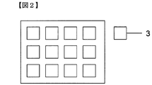
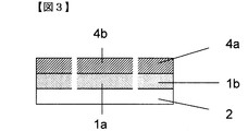
- a half cut is performed using the blade of a shape as shown in FIG. A cross section of the half-cut adhesive film is shown in FIG.
- Process B is a process of peeling only the unnecessary cover film (c) of the adhesive film after half-cutting.
- the area shown by 4a in FIG. 4 is an unnecessary part of the cover film (c). Yes, only that part is peeled off.
- the peeling method include a method of pulling up the cover film (c).
- the peeling angle is not particularly limited, but is preferably 45 ° to 90 °. At this angle, the adhesive layer (b) can be peeled without tearing or the like. After the cover film (c) is peeled off, the adhesive layer (b) is exposed at the unnecessary portion, and the state shown in FIG. 5 is obtained.
- Process C is a process of attaching an adhesive tape to the cover film (c) side of the adhesive film.
- Adhesive tape is applied to the entire surface of the adhesive film in the state shown in FIG.
- the method for attaching the adhesive tape is not particularly limited, and examples thereof include a method of pressing and laminating with a roll or the like.
- the pressure-sensitive adhesive tape preferably has a support film (a ′) and an adhesive layer (b ′).
- a ′ polyolefin can be preferably used because of its high flexibility. By using such a flexible film, it becomes easier to suppress cracks and breakage at the time of peeling of the adhesive layer (b ′).
- the thickness of the support film (a ′) is preferably 25 ⁇ m or less and more preferably 15 ⁇ m or less because the adhesive layer (b ′) is less likely to break when the adhesive layer (b ′) is peeled off. From the viewpoint of handleability, the thickness of the support film (a ′) is preferably 3 ⁇ m or more.
- the thickness of the entire adhesive tape is not particularly limited, but is preferably 10 to 40 ⁇ m. Within this range, the transportability is ensured, and the peeling of the adhesive layer (b) at the time of peeling can be reduced.
- Process D is a process of peeling the unnecessary adhesive layer (b) and the target cover film (c) of the adhesive film together with the adhesive tape.
- the target adhesive layer (b) as shown in FIG. 1 becomes the support film (a).
- the adhesive sheet present above is obtained.
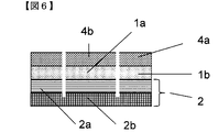
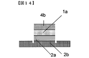
- a film having a two-layer structure that can be peeled off at the interface is used as the support film (a), and the upper layer in contact with the adhesive of the two layers is completely cut during the half-cutting in the step A.
- the lower layer that is not in contact with the adhesive layer is a half cut that does not cut completely, and the unnecessary portion in Step D is peeled off at the interface between the two layers, so that the individual adhesive layer as shown in FIG.
- An adhesive sheet in which (b) is present on the support film (a) is obtained.
- step D in order to facilitate peeling at the interface between the two layers, it is preferable to select each material so that the peeling strength between the two layers is smaller than the peeling strength at the interface between the adhesive layer and the upper layer of the support film. .
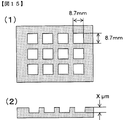
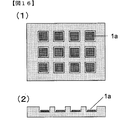
- the adhesive sheet having the structure as shown in FIG. 6 can be preferably used when the singulated adhesive is applied to a place recessed from the surroundings, and when the depression is deep or the aspect ratio of the depression space is large, It can be preferably used when the depth of the dent is larger than the size of the dent opening.
- the adhesive sheet is attached to a concave place surrounded by a solder resist or a wiring layer on the wiring board. When used for such attachment, if the sum of the thickness of the upper layer of the support film having a two-layer structure and the thickness of the adhesive layer is equal to or greater than the depth of the recess, it is separated into the bottom of the recess. It is easy to apply the adhesive without deformation or lifting of the edge of the adhesive.
- the adhesive sheet (b) is less likely to break due to stress during peeling.
- the stress on the adhesive layer (b) at the time of peeling increases as the peeling angle increases, and increases as the stiffness of the adhesive tape increases. Therefore, it is preferable that the adhesive tape is thin as long as the material is the same as long as it is not difficult to convey, and the peel angle is preferably as small as possible in a peelable range.
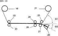
- the peeling angle between the pressure-sensitive adhesive tape and the adhesive sheet at the time of peeling preferably satisfies the following relationship. That is, as shown in FIG. 6, when the bending angle of the pressure-sensitive adhesive tape is ⁇ 1 and the bending angle of the support film (a) is ⁇ 2 , it is preferable that ⁇ 1 and ⁇ 2 simultaneously satisfy the following relationship.
- ⁇ 1 is defined as an angle formed by an extension line in the pulling direction of the adhesive tape and an extension line of the adhesive sheet before peeling
- ⁇ 2 is an adhesive sheet in which the extending line in the pulling direction of the support film (a) is before peeling. It is defined as the angle formed by the extension line.
- the temperature it is preferable to set the temperature to 35 ° C. or higher at the time of peeling because the adhesive layer (b) becomes soft and can suppress chipping and breakage. Moreover, when it is 70 degrees C or less, since the adhesive bond layer (b) does not become too soft and the shape and film thickness of an individualized part are maintained, it is preferable.
- the manufacturing method of the wiring board having the separated adhesive layer (b) according to the present invention includes the adhesive layer (b) side surface of the adhesive sheet obtained by the above manufacturing method, and the wiring side of the wiring board. Are aligned, and a laminate of an adhesive sheet and a wiring board is formed by vacuum lamination or vacuum press, and then the support film (a) of the adhesive sheet is removed.
- the adhesive sheet having the adhesive layer (b) singulated on the support film (a) obtained after the step D has an adhesive layer (b) side surface and a wiring side surface of the wiring board. It can be used by aligning and forming a laminate of an adhesive sheet and a wiring board by vacuum lamination or vacuum pressing. A vacuum press or a vacuum laminate can be suitably used because it hardly causes air bubbles to be caught between the wiring board and the adhesive layer (b).
- the adhesive sheet having the separated adhesive layer (b) is not particularly limited in aligning the surface on the adhesive layer (b) side and the surface on the wiring side of the wiring board, but is formed on both sides.
- a specific shape for recognizing the position may be recognized by a camera.
- the adhesive sheet and the wiring board may be provided with through holes at specific locations where they should overlap, and a pin may be inserted so as to penetrate them.
- the through hole may be formed by full-cutting only this portion during half-cut processing, or may be formed in a separate process.
- a plurality of individual adhesive layers (b) may be laminated on the wiring board at once, or may be performed for each individual piece.
- a plurality of adhesive layers (b) separated by a plurality of heads may be individually pressed or laminated.
- an individual adhesive layer for temporary fixing that is not used for bonding to the wiring board may be provided, and temporary fixing immediately after alignment may be performed.
- the wiring board having the adhesive layer (b) singulated at a specific position can be obtained by removing the support film (a) of the adhesive sheet.
- the transfer of the adhesive layer (b) to the wiring board may be performed as it is using an adhesive sheet, or a piece obtained by cutting the adhesive sheet may be used.
- an adhesive sheet in which the adhesive layer (b) is continuously present on the support film (a) as shown in FIG. 8 is prepared, and the adhesive sheet is cut to a desired length. You may transfer after processing into strip shape as shown.
- the method for manufacturing a semiconductor device of the present invention is a method for mounting a semiconductor element on the wiring board.
- the wiring board having the adhesive layer separated into the specific positions can be used for manufacturing a semiconductor device by mounting the semiconductor element on the wiring board through the adhesive layer.
- a semiconductor chip with bumps formed of Au or Cu is connected to the wiring of the wiring board via an adhesive layer, and then the semiconductor chip and the wiring board are sealed with a mold resin
- a semiconductor device can be manufactured.
- the adhesive sheet manufacturing apparatus of the present invention includes a half-cut device, a cover film peeling device, an adhesive tape applying device, and an adhesive tape peeling device in this order.
- the half-cut device is not particularly limited as long as it is a device that can locally cut only the adhesive layer (b) and the cover film (c) by local half-cutting. Will be described with reference to FIG.
- the adhesive film 6 is pulled out from the adhesive film delivery roll 7 by applying a force to grip and pull out one of the adhesive films 6 using the adhesive film drawer clamp 13.
- the adhesive film 6 is sent to the adhesive film tension roll 11 through the transport roll (1) 8 and the transport roll (2) 9.
- This adhesive film tension roll 11 can be processed on the stage of the adsorption fixing stage (1) 12 by cutting the adhesive film 6 using the adhesive film cutting blade 10 while suppressing the slack of the adhesive film 6. Magnitude.
- the adhesive film 6 on the stage of the adsorption fixing stage (1) 12 is subjected to local half-cutting using the half-cutting blade 3 attached to the upper plate 14, and the adhesive layer (b) and Only the cover film (c) is cut locally.
- the upper plate 14 is movable up and down, and is moved in the direction of the suction fixing stage (1) 12 to press the blade 3 for half-cut against the adhesive film 6 so as to cover the cover film (c) and the adhesive layer.
- (B) can be cut and the support film (a) can be half cut.
- these mechanisms can be used to cut out the adhesive part left on the support film (a) for mounting the semiconductor.
- the upper plate 14 is provided with a blade for forming the through hole 15 in addition to the blade 3 for half cut.
- the through-hole 15 can be formed in the adhesive film 6, and it can be used for positioning as described above.
- the blade for through-hole 15 formation is a half-cut blade. It needs to be higher than 3 by the necessary amount.
- the cover film peeling apparatus is not particularly limited as long as only the cover film (c) of the unnecessary part of the adhesive film after half-cutting can be peeled off, but will be described with reference to FIG. 11 as an example.
- the cover film peeling apparatus adsorbs the surface on the support film (a) side of the adhesive film 6 on the adsorption fixing stage (2) 16. Further, the cover film (c) adsorption (adhesion) arm 17 is adsorbed to the end of the adhesive film 6.
- the cover film (c) can be peeled by moving the cover (c) suction (adhesion) arm 17 in a direction away from the suction fixing stage (2). Thereby, the cover film (c) on the adhesive film 6 after a half cut can be peeled. Under the present circumstances, the cover film (c) of the part cut by half cut is not peeled.
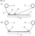
- the adhesive tape attaching device is not particularly limited as long as the adhesive tape can be attached to the cover film (c) side of the adhesive film, but will be described with reference to FIG.
- the pressure-sensitive adhesive tape 5 unwound from the pressure-sensitive adhesive tape unwinding roll 18 is pressed by the pressure-sensitive adhesive tape end pressing roll 19 against the adhesive film 6 from which the unnecessary cover film (c) has been peeled off by the cover film peeling device.
- the pressure-sensitive adhesive tape laminating roll 20 is movable, and is pressed against the adhesive film 6 adsorbed on the suction fixing stage (2) 16 at a position adjacent to the pressure-sensitive tape end pressing roll 19, and from that position to the right It moves to a direction (FIG. 12 (1)), and finally moves to the right end of the adhesive film 6 (FIG. 12 (2)). Thereby, the adhesive tape 5 can be laminated on the adhesive film 6.
- the adhesive tape peeling device is not particularly limited as long as the adhesive layer (b) of the unnecessary part of the adhesive film and the cover film (c) of the target part can be peeled together with the adhesive tape, but FIG. 12 is used as an example. I will explain.
- the adsorption fixing stage (2) 16 is separated from the adhesive film 6, and the adhesive tape unwinding roll 18 and the adhesive tape end pressing roll 19 are also provided. Separate from the adhesive tape 5.
- FIG. 12 shows a peeling end fixing roll (1) 22, a peeling end fixing roll (2) 23, a peeling moving roll (1) 24, a peeling moving roll (2) 25, a peeling moving roll (3) 26, A peeling moving roll (4) 27 and a peeling clamp 28 are installed.
- the peeling clamp 28 has a mechanism capable of grasping the end of the adhesive film 6 and moving downward. Further, the separation moving roll (1) 24, the separation movement roll (2) 25, the separation movement roll (3) 26, and the separation movement roll (4) 27 are provided so that the magnitudes of ⁇ 1 and ⁇ 2 shown in FIG. 12 can be adjusted. Thus, the relative position with the adhesive tape take-up roll 21 is determined. Moreover, these peeling movement rolls may be provided with the heating mechanism.
- the relative positions of these peeling moving rolls to the adhesive tape take-up roll 21 are moved to the left in FIG. 12 while controlling ⁇ 1 and ⁇ 2 .
- the pressure-sensitive adhesive tape take-up roll 21 is rotated to wind the pressure-sensitive adhesive tape 5 to remove the unnecessary part of the adhesive layer (b) and the target part of the cover film (c) on the adhesive film 6. it can.
- all or a part of these peeling and moving rolls may be heated to heat the adhesive film 6.
- the adhesive sheet of the present invention can be obtained.
- melt viscosity The obtained sample was cut out into a circular shape of ⁇ 15 mm, and melt viscosity was measured using a TA Instruments rheometer (AR-G2) at a strain rate of 1%, a frequency of 1 Hz, and a heating rate of 5 ° C / min. Was measured.
- AR-G2 TA Instruments rheometer
- the adhesive film was cut into a width of 20 mm, and the support film (a) side The surface was affixed to a SUS substrate using a double-sided tape.
- the cover film (c) is peeled in the 90 ° direction and set in a tensile tester (Tensilon, manufactured by Orientec Co., Ltd.), and the peeling speed is 50 mm / min in the 90 ° direction. Then, the force required for peeling was measured, and the peeling force at 25 ° C. between the adhesive layer (b) and the cover film (c) was obtained.
- a tensile tester Teensilon, manufactured by Orientec Co., Ltd.
- the cover film (c) was peeled from the adhesive film, and the adhesive layer (b) side was attached to a SUS substrate using a double-sided tape.
- the support film (a) is peeled off in the 90 ° direction and set in a tensile test apparatus (manufactured by Orientec Co., Ltd., Tensilon), and the peeling speed is 50 mm / min in the 90 ° direction. Then, the force required for peeling was measured, and the peeling force at 25 ° C. between the adhesive layer (b) and the support film (a) was obtained.
- Polyimide resin Synthesis of polyimide resin 1 Under a dry nitrogen stream, 24.54 g (0.067 mol) of 2,2-bis (3-amino-4-hydroxyphenyl) hexafluoropropane (hereinafter referred to as BAHF), 1,3-bis (3 -Aminopropyl) 4.97 g (0.02 mol) of tetramethyldisiloxane (hereinafter referred to as SiDA) and 1.86 g (0.02 mol) of aniline as an end-capping agent were dissolved in 80 g of NMP.
- BAHF 2,2-bis (3-amino-4-hydroxyphenyl) hexafluoropropane
- SiDA 1,3-bis (3 -Aminopropyl) 4.97 g (0.02 mol) of tetramethyldisiloxane
- aniline as an end-capping agent
- ODPA bis (3,4-dicarboxyphenyl) ether dianhydride
- the precipitate was collected by filtration, washed three times with water, and then dried at 80 ° C. for 100 hours using a vacuum dryer.
- absorption peaks of an imide structure attributed to polyimide were detected in the vicinity of 1,780 cm ⁇ 1 and 1,377 cm ⁇ 1 .
- a polyimide resin 2 having a weight average molecular weight of about 30,000 was obtained.
- the mixture was stirred to disperse the filler and the curing accelerator particles.
- the obtained adhesive varnish was applied to a treated surface of a 38 ⁇ m-thick polyethylene terephthalate film (AL-5 treatment, manufactured by Lintec Corporation) as a base film using a comma coater (coating machine).
- a protective film (SK-1 treatment, manufactured by Lintec Corporation) having a thickness of 25 ⁇ m was bonded to the adhesive layer (b) at 70 ° C. to obtain an adhesive film 1.
- the base film serves as the support film (a)
- the protective film serves as the cover film (c).
- the cover film (c) was peeled from the adhesive film 1 and bonded at 60 ° C. so that the adhesive layers (b) face each other.
- One support film (a) of the bonded sample was peeled off and further bonded, and the layers were laminated until the thickness of the adhesive layer (b) became 800 ⁇ m.
- the melt viscosity of the sample obtained by peeling the support film (a) was measured with a rheometer
- the melt viscosity at 100 ° C. was 700 Pa ⁇ s.
- the peeling force between them was 5 N / m.
- the base film is the support film (a)
- the protective film is the cover film (c).
- the melt viscosity at 100 ° C. was 700 Pa ⁇ s
- the peel force between the support film (a) and the adhesive layer (b) was 30 N / m
- the cover film The peeling force between (c) and the adhesive layer (b) was 5 N / m.
- the difference from the adhesive film 1 is the release treatment of the support film (a), and the physical properties other than the difference in adhesive force due to the difference are the same as those of the adhesive film 1.
- Adhesive Film 3 25 g of polyimide resin 2 obtained by synthesis, 30 g of solid epoxy compound 157S70, 45 g of curing accelerator Novacure HX-3941HP, 100 g of filler SO-E2, and 80 g of solvent methyl isobutyl ketone were prepared. The mixture was stirred to disperse the filler and the curing accelerator particles. The obtained adhesive varnish was applied to a treated surface of a 38 ⁇ m-thick polyethylene terephthalate film (AL-5 treatment, manufactured by Lintec Corporation) as a base film using a comma coater (coating machine). Was dried for 10 minutes to form an adhesive layer (b) having a dry thickness of 32 ⁇ m.
- A-5 treatment manufactured by Lintec Corporation
- a protective film (SK-1 treatment, manufactured by Lintec Corporation) having a thickness of 25 ⁇ m was bonded to the adhesive layer (b) at 70 ° C. to obtain an adhesive film 3.
- the base film is the support film (a)
- the protective film is the cover film (c).
- the cover film (c) was peeled from the adhesive film 3 and bonded at 80 ° C. so that the adhesive layers (b) face each other.
- One support film (a) of the bonded sample was peeled off and further bonded, and the layers were laminated until the thickness of the adhesive layer (b) became 800 ⁇ m. Thereafter, when the melt viscosity of the sample obtained by peeling off the support film (a) was measured with a rheometer, the melt viscosity at 100 ° C. was 2,500 Pa ⁇ s.
- Adhesive Film 4 25 g of phenoxy resin YP-50, 30 g of solid epoxy compound 157S70, 45 g of curing accelerator Novacure HX-3941HP, 100 g of filler SO-E2, and 80 g of solvent toluene were prepared and stirred. The filler and the curing accelerator particles were dispersed. The obtained adhesive varnish was applied to a treated surface of a 38 ⁇ m thick polyethylene terephthalate film (38E-NSH, manufactured by Fujimori Sangyo Co., Ltd.) as a base film using a comma coater (coating machine). Was dried for 10 minutes to form an adhesive layer (b) having a dry thickness of 32 ⁇ m.
- 38E-NSH polyethylene terephthalate film
- a protective film (AL-5 treatment, manufactured by Lintec Co., Ltd.) having a thickness of 25 ⁇ m was bonded to the adhesive layer (b) at 80 ° C. to obtain an adhesive film 4.
- the base film is the support film (a)
- the protective film is the cover film (c).
- the cover film (c) was peeled from the adhesive film 4 and bonded at 80 ° C. so that the adhesive layers (b) face each other.
- One support film (a) of the bonded sample was peeled off and further bonded, and the layers were laminated until the thickness of the adhesive layer (b) became 800 ⁇ m.
- the melt viscosity at 100 ° C. was 7,000 Pa ⁇ s.
- ⁇ Adhesive tape> 31B manufactured by Nitto Denko Corporation, 53 ⁇ m thickness
- No. 603 # 25 manufactured by Teraoka Manufacturing Co., Ltd., total thickness: 34 ⁇ m, two-layer structure of support film (polyester, thickness 25 ⁇ m) and adhesive layer (thickness 9 ⁇ m))
- the adhesive film 1 is fixed to the experimental table with the cover film (c) side up, and 31B tape is attached to the cover film (c) side of the adhesive film using a roller, and 31B A sheet with a tape attached was obtained.
- Example 1 The adhesive part of the obtained adhesive sheet was inspected for cracks and the like, and the number of defective parts (number of successes) was counted. The results are shown in Table 1. (Examples 3 to 5) It is the theta 1 except for changing as shown in Table 1, to obtain an adhesive sheet in the same manner as in Example 1. The adhesive part of the obtained adhesive sheet was inspected for cracks and the like, and the number of defective parts (number of successes) was counted. The results are shown in Table 1. (Examples 6 to 8) An adhesive sheet was obtained in the same manner as in Example 2 except that ⁇ 2 was changed as shown in Table 2. The adhesive part of the obtained adhesive sheet was inspected for cracks and the like, and the number of defective parts (number of successes) was counted.
- Example 9 As an adhesive tape, no. An adhesive sheet was obtained in the same manner as in Example 1 except that 603 # 25 was used. No. When affixing 603 # 25 to the cover film (c) side of the adhesive film, the surface on the adhesive layer side was matched with the surface on the cover film (c) side. The adhesive part of the obtained adhesive sheet was inspected for cracks and the like, and the number of defective parts (number of successes) was counted. The results are shown in Table 2. (Example 10) As an adhesive tape, no. An adhesive sheet was obtained in the same manner as in Example 2 except that 603 # 25 was used. No.
- Example 11 As an adhesive tape, no. An adhesive sheet was obtained in the same manner as in Example 1 except that 631U # 12 was used. No. When 631U # 12 was attached to the cover film (c) side of the adhesive film, the surface on the adhesive layer side was aligned with the surface on the cover film (c) side.
- Example 12 As an adhesive tape, no. An adhesive sheet was obtained in the same manner as in Example 2 except that 631U # 12 was used. No. When 631U # 12 was attached to the cover film (c) side of the adhesive film, the surface on the adhesive layer side was aligned with the surface on the cover film (c) side. The adhesive part of the obtained adhesive sheet was inspected for cracks and the like, and the number of defective parts (number of successes) was counted. The results are shown in Table 3.
- Example 13 and 15 It is the theta 1 except for changing as shown in Table 3, to obtain an adhesive sheet in the same manner as in Example 11. The adhesive part of the obtained adhesive sheet was inspected for cracks and the like, and the number of defective parts (number of successes) was counted. The results are shown in Table 3. (Examples 14 and 16) It is the theta 2 except for changing as shown in Table 3, to obtain an adhesive sheet in the same manner as in Example 12. The adhesive part of the obtained adhesive sheet was inspected for cracks and the like, and the number of defective parts (number of successes) was counted. The results are shown in Table 3.
- Example 17 Place the adhesive film 2 on the pinnacle blade (manufactured by Tsukaya Cutlery Co., Ltd.) with 16 8.5 mm square square blades so that the cover film (c) side is in contact with the pinnacle blade, Using a rotary die cutter (manufactured by Tsukaya Cutlery Co., Ltd.), the cover film (c) and the adhesive layer (b) were half cut. After half-cutting, one end of the cover film (c) was pulled to remove unnecessary portions of the cover film (c). After removing the unnecessary portion, the adhesive film 1 was fixed to the experimental table with the cover film (c) side up, No.
- 631U # 12 adhesive layer side surface was affixed to the cover film (c) side of the adhesive film 2 using a roller. A sheet to which 631U # 12 was attached was obtained.
- an adhesive sheet having 16 8.5 mm square adhesives formed on the support film (a) was obtained. The adhesive part of the obtained adhesive sheet was inspected for cracks and the like, and the number of defective parts (number of successes) was counted. The results are shown in Table 4.
- Example 18 and 19 An adhesive sheet was obtained in the same manner as in Example 17 except that the adhesive film was changed as shown in Table 4. The adhesive part of the obtained adhesive sheet was inspected for cracks and the like, and the number of defective parts (number of successes) was counted. The results are shown in Table 4.
- Example 20 An adhesive sheet was obtained in the same manner as in Example 1 except that UHP0810AT was used instead of 31B as the adhesive tape. In addition, when UHP0810AT was affixed on the cover film (c) side of the adhesive film, the surface on the adhesive layer side was aligned with the surface on the cover film (c) side. The adhesive part of the obtained adhesive sheet was inspected for cracks and the like, and the number of defective parts (number of successes) was counted. The results are shown in Table 5.
- Example 21 An adhesive sheet was obtained in the same manner as in Example 2 except that UHP0810AT was used instead of 31B as the adhesive tape. In addition, when UHP0810AT was affixed on the cover film (c) side of the adhesive film, the surface on the adhesive layer side was aligned with the surface on the cover film (c) side.
- Example 5 The adhesive part of the obtained adhesive sheet was inspected for cracks and the like, and the number of defective parts (number of successes) was counted. The results are shown in Table 5.
- Examples 22 and 24 It is the theta 1 except for changing as shown in Table 5, to obtain an adhesive sheet in the same manner as in Example 20.
- the adhesive part of the obtained adhesive sheet was inspected for cracks and the like, and the number of defective parts (number of successes) was counted.
- Table 5 It is the theta 2 except for changing as shown in Table 5, to obtain an adhesive sheet in the same manner as in Example 21.
- Example 26 Place the adhesive film 2 on the pinnacle blade (manufactured by Tsukaya Cutlery Co., Ltd.) with 16 8.5 mm square square blades so that the cover film (c) side is in contact with the pinnacle blade, Using a rotary die cutter (manufactured by Tsukaya Cutlery Co., Ltd.), the cover film (c) and the adhesive layer (b) were half cut. After half-cutting, one end of the cover film (c) was pulled to remove unnecessary portions of the cover film (c).
- the adhesive film 2 is fixed to the experimental table with the cover film (c) side up, and the surface of the adhesive layer side of UHP0810AT is placed on the cover film (c) side of the adhesive film 2 And a sheet on which UHP0810AT was adhered was obtained.
- Example 7 An adhesive sheet was obtained in the same manner as in Example 26 except that the adhesive film was changed as shown in Table 7. The adhesive part of the obtained adhesive sheet was inspected for cracks and the like, and the number of defective parts (number of successes) was counted. The results are shown in Table 7.
- Example 29 Place the adhesive film 1 on the pinnacle blade (manufactured by Tsukaya Cutlery Co., Ltd.) having 16 8.5 mm square square blades so that the cover film (c) side is in contact with the pinnacle blade, Using a rotary die cutter (manufactured by Tsukaya Cutlery Co., Ltd.), the cover film (c) and the adhesive layer (b) were half cut. After half-cutting, one end of the cover film (c) was pulled to remove unnecessary portions of the cover film (c). After removing the unnecessary portion, the adhesive film 1 is fixed on a hot plate controlled so that the surface temperature of the adhesive film 1 is 30 ° C.
- the 31B tape is adhesive
- the sheet was attached to the cover film (c) side of the film using a roller to obtain a sheet on which the 31B tape was attached.
- the temperature control of the hot plate was performed by measuring the surface temperature of the adhesive film 1 with a thermocouple.
- an adhesive sheet having 16 8.5 mm square adhesives formed on the support film (a) was obtained.
- the adhesive part of the obtained adhesive sheet was inspected for cracks and the like, and the number of defective parts (number of successes) was counted.
- Example 30 to 33 An adhesive sheet was obtained in the same manner as in Example 29 except that the surface temperature of the adhesive film 1 by the hot plate was changed as shown in Table 8. In Example 33, no cracks and defects were observed, but deformation of the adhesive layer (b) was observed.
- Example 34 631S2 # 50 (manufactured by Teraoka Seisakusho Co., Ltd.) PET film with pressure-sensitive adhesive (PET film thickness 50 ⁇ m, total including pressure-sensitive adhesive layer) on the surface of the adhesive film 1 opposite to the surface where the adhesive layer is formed
- PET film thickness 50 ⁇ m, total including pressure-sensitive adhesive layer A film having a thickness of 85 ⁇ m and a laminate adhesive strength of 6.7 N / m with a PET film is used as an adhesive film with a two-layer support film, which is used instead of the adhesive film 1 and has a thickness direction of 630 # 75.
- An adhesive sheet was obtained in the same manner as in Example 20 except that half-cutting was performed halfway. The adhesive part of the obtained adhesive sheet was inspected for cracks and the like, and the number of defective parts (number of successes) was counted. The success number was 16 out of 16.
- the structure of the separated part of the obtained adhesive sheet was the same as that shown in FIG.
- the adhesive sheet which has arrange
- the wiring for flip-chip mounting of a semiconductor Expansion to substrates can be expected.
- the adhesive sheet of the present invention is effective for highly accurate attachment of a brittle adhesive having high fluidity, such as a non-conductive film (NCF) for semiconductor mounting, to a wiring board.
- NCF non-conductive film
Landscapes
- Engineering & Computer Science (AREA)
- Manufacturing & Machinery (AREA)
- Chemical & Material Sciences (AREA)
- Microelectronics & Electronic Packaging (AREA)
- Organic Chemistry (AREA)
- Mechanical Engineering (AREA)
- Health & Medical Sciences (AREA)
- Chemical Kinetics & Catalysis (AREA)
- Medicinal Chemistry (AREA)
- Polymers & Plastics (AREA)
- Materials Engineering (AREA)
- Adhesive Tapes (AREA)
- Adhesives Or Adhesive Processes (AREA)
- Wire Bonding (AREA)
Abstract
Description
特許文献4、5、6で開示された通常のハーフカットの手法は、接着剤層に靭性があり、接着剤層単独で引っ張りや搬送などに耐えられる材料を前提に設計されており、接着剤層が脆弱で、単独では引っ張りや搬送などに耐えられない材料には適用できなかった。
支持フィルム(a)上に個片化された接着剤層(b)を有する接着剤シートの製造方法であって、
工程A:支持フィルム(a)、接着剤層(b)およびカバーフィルム(c)をこの順に有する接着剤フィルムを、局所的なハーフカットにより、接着剤層(b)およびカバーフィルム(c)のみを局所的に切断する工程、
工程B:前記接着剤フィルムの不要部のカバーフィルム(c)のみを剥離する工程、
工程C:前記接着剤フィルムのカバーフィルム(c)側に、粘着テープを貼り付ける工程、
工程D:前記接着剤フィルムの不要部の接着剤層(b)および目的部のカバーフィルム(c)を、粘着テープとともに剥離する工程、
をこの順で有する接着剤シートの製造方法、である。
ここで、「不要部」とは、剥離されて最終的には接着剤シートに残らない部分をいう。
上記製造方法により得られた接着剤シートの接着剤層(b)側の面と、配線基板の配線側の面を位置あわせし、真空ラミネートまたは真空プレスによって接着剤シートと配線基板の積層体とし、次に接着剤シートの支持フィルム(a)を除去する配線基板の製造方法、である。
上記配線基板の製造方法により得られた配線基板に半導体素子を実装する半導体装置の製造方法、である。
ハーフカット装置、カバーフィルム剥離装置、粘着テープ貼付装置および粘着テープ剥離装置をこの順に備えている接着剤シートの製造装置、である。
本発明の個片化された接着剤層を有する接着剤シートの製造方法は、支持フィルム(a)が積層界面で剥離可能な2層構造であることが好ましい。
本発明の個片化された接着剤層を有する接着剤シートの製造方法は、前記粘着テープが、支持フィルム(a’)および接着剤層(b’)を有しており、前記支持フィルム(a’)がポリオレフィンであることが好ましい。
本発明の個片化された接着剤層を有する接着剤シートの製造方法は、前記粘着テープの厚みが10~40μmであることが好ましい。
本発明の個片化された接着剤層を有する接着剤シートの製造方法は、前記工程Dにおける剥離が、粘着テープの折り曲げ角度をθ1、支持フィルム(a)の折り曲げ角度をθ2として、これらが下式(I)、(II)を満たすことが好ましい。
|θ1|<|θ2|・・・(I)
|θ1|+|θ2|<60°・・・(II)
工程A:支持フィルム(a)、接着剤層(b)およびカバーフィルム(c)をこの順に有する接着剤フィルムを、局所的なハーフカットにより、接着剤層(b)およびカバーフィルム(c)のみを局所的に切断する工程、
工程B:前記接着剤フィルムの不要部のカバーフィルム(c)のみを剥離する工程、
工程C:前記接着剤フィルムのカバーフィルム(c)側に、粘着テープを貼り付ける工程、
工程D:前記接着剤フィルムの不要部の接着剤層(b)および目的部のカバーフィルム(c)を、粘着テープとともに剥離する工程、
をこの順で有する。
|θ1|<|θ2|・・・(I)
|θ1|+|θ2|<60°・・・(II)
接着剤層(b)と支持フィルム(a)の剥離の際にかかる応力に対して、θ2よりもθ1の方が影響が大きい。そのため、|θ1|+|θ2|=一定の条件では、|θ1|<|θ2|とすることにより接着剤層(b)への応力を小さく抑えられる。また、|θ1|+|θ2|<60°であれば、剥離時の接着剤層(b)への応力が大きくなりすぎず、カケや破断などを抑制することができる。なお接着剤層(b)のカケや破断はダストの原因となるため、目的部の接着剤層(b)だけでなく不要部の接着剤層(b)についても、カケや破断は抑制することが好ましい。
(1)ポリイミド樹脂の赤外吸収スペクトルの測定
堀場製作所製FT-IR720を用いてKBr法により測定した。
(2)ポリイミド樹脂の重量平均分子量の測定
ゲルパーミエーションクロマトグラフィー(日本ウォーターズ(株)製 Waters 2690)を用い、ポリスチレン換算で重量平均分子量を求めた。カラムは東ソー(株)製 TOSOH TXK-GEL α-2500、およびα-4000を用い、移動層にはN-メチル-2-ピロリドン(以下、NMP)を用いた。
(3)溶融粘度の測定
得られたサンプルをφ15mmの円形に切り抜き、TAインスツルメンツ社製レオメータ(AR-G2)を用いて、歪1%、周波数1Hz、5℃/分の昇温速度で溶融粘度を測定した。
(4)接着剤層(b)と支持フィルム(a)、カバーフィルム(c)の間の25℃における剥離力の測定
接着剤フィルムを20mm幅に切断し、これの支持フィルム(a)側の面を、両面テープを用いてSUS製の基板に貼り付けた。25℃に調温された測定室で、カバーフィルム(c)を90°方向に剥離させて引っ張り試験装置((株)オリエンテック製、テンシロン)にセットし、90°方向に剥離速度50mm/分で引っ張り、剥離に必要な力を測定し、接着剤層(b)とカバーフィルム(c)の間の25℃における剥離力とした。
<ポリイミド樹脂>
ポリイミド樹脂1の合成
乾燥窒素気流下、2,2-ビス(3-アミノ-4-ヒドロキシフェニル)ヘキサフルオロプロパン(以下、BAHF)24.54g(0.067モル)、1,3-ビス(3-アミノプロピル)テトラメチルジシロキサン(以下、SiDAとする)4.97g(0.02モル)、末端封止剤として、アニリン1.86g(0.02モル)をNMP80gに溶解させた。ここにビス(3,4-ジカルボキシフェニル)エーテル二無水物(以下、ODPA)31.02g(0.1モル)をNMP20gとともに加えて、20℃で1時間反応させ、次いで50℃で4時間撹拌した。その後、キシレンを15g添加し、水をキシレンとともに共沸させながら、180℃で5時間攪拌した。攪拌終了後、溶液を水3Lに投入して白色沈殿したポリマーを得た。この沈殿をろ過して回収し、水で3回洗浄した後、真空乾燥機を用いて80℃、20時間乾燥した。得られたポリマー固体の赤外吸収スペクトルを測定したところ、1,780cm-1付近、1,377cm-1付近にポリイミドに起因するイミド構造の吸収ピークが検出された。重量平均分子量がおよそ25,000のポリイミド樹脂1を得た。
乾燥窒素気流下、2,2-ビス(4-(3,4-ジカルボキシフェノキシ)フェニル)プロパン二無水物(以下、BPADA)52g(0.1モル)、SiDA10.93g(0.044モル)、1,3‐ビス(3-アミノフェノキシ)ベンゼン15.91g(0.055モル)をNMP200gに溶解させた。次いで70℃で1時間撹拌した。その後、190℃で3時間攪拌した。攪拌終了後、溶液を水3Lに投入して白色沈殿したポリマーを得た。この沈殿をろ過して回収し、水で3回洗浄した後、真空乾燥機を用いて80℃、100時間乾燥した。得られたポリマー固体の赤外吸収スペクトルを測定したところ、1,780cm-1付近、1,377cm-1付近にポリイミドに起因するイミド構造の吸収ピークが検出された。重量平均分子量がおよそ30,000のポリイミド樹脂2を得た。
YP-50(重量平均分子量60,000~80,000、新日鐵化学(株)製)
<固形エポキシ化合物>
157S70(商品名、三菱化学(株)製)
<硬化促進剤>
マイクロカプセル型硬化促進剤 ノバキュアHX-3941HP(商品名、旭化成イーマテリアルズ(株)製)
<フィラー>
SO-E2(商品名、(株)アドマテックス製、球形シリカ粒子、平均粒子径0.5μm)
接着剤フィルム1の作製および評価
合成で得たポリイミド樹脂1を25g、固形エポキシ化合物157S70を30g、硬化促進剤ノバキュアHX-3941HPを45g、フィラーSO-E2を100g、溶剤メチルイソブチルケトン80gを調合し、攪拌してフィラーおよび硬化促進剤粒子の分散処理を行った。得られた接着剤ワニスを、コンマコーター(塗工機)を用いてベースフィルムである厚さ38μmのポリエチレンテレフタレートフィルム(AL-5処理、リンテック(株)製)の処理面に塗布し、90℃で10分間乾燥を行って乾燥厚み32μmの接着剤層(b)を形成させた。接着剤層(b)に厚さ25μmの保護フィルム(SK-1処理、リンテック(株)製)を70℃で貼りあわせ接着剤フィルム1を得た。なお接着剤フィルム1においては、ベースフィルムが支持フィルム(a)となり、保護フィルムがカバーフィルム(c)となる。
ベースフィルムとして、38μmのポリエチレンテレフタレートフィルム(38E-NSH、フジモリ産業(株)製)を使用する以外は、上記接着剤フィルム1の作成製と同一の手順で接着剤フィルム2を作製した。接着剤フィルム2においては、ベースフィルムが支持フィルム(a)となり、保護フィルムがカバーフィルム(c)となる。また上記接着剤フィルム1と同様にして、評価したところ、100℃の溶融粘度は700Pa・s、支持フィルム(a)と接着剤層(b)間の剥離力は30N/mであり、カバーフィルム(c)と接着剤層(b)間の剥離力は5N/mであった。接着剤フィルム1との相違点は、支持フィルム(a)の離型処理であり、その差により密着力が異なる点以外の物性は接着剤フィルム1と同等であった。
合成で得たポリイミド樹脂2を25g、固形エポキシ化合物157S70を30g、硬化促進剤ノバキュアHX-3941HPを45g、フィラーSO-E2を100g、溶剤メチルイソブチルケトン80gを調合し、攪拌してフィラーおよび硬化促進剤粒子の分散処理を行った。得られた接着剤ワニスを、コンマコーター(塗工機)を用いてベースフィルムである厚さ38μmのポリエチレンテレフタレートフィルム(AL-5処理、リンテック(株)製)の処理面に塗布し、90℃で10分間乾燥を行って乾燥厚み32μmの接着剤層(b)を形成させた。接着剤層(b)に厚さ25μmの保護フィルム(SK-1処理、リンテック(株)製)を70℃で貼りあわせ接着剤フィルム3を得た。なお接着剤フィルム3においては、ベースフィルムが支持フィルム(a)となり、保護フィルムがカバーフィルム(c)となる。
フェノキシ樹脂YP-50を25g、固形エポキシ化合物157S70を30g、硬化促進剤ノバキュアHX-3941HPを45g、フィラーSO-E2を100g、溶剤トルエン80gを調合し、攪拌してフィラーおよび硬化促進剤粒子の分散処理を行った。得られた接着剤ワニスを、コンマコーター(塗工機)を用いてベースフィルムである厚さ38μmのポリエチレンテレフタレートフィルム(38E-NSH、フジモリ産業(株)製)の処理面に塗布し、90℃で10分間乾燥を行って乾燥厚み32μmの接着剤層(b)を形成させた。接着剤層(b)に厚さ25μmの保護フィルム(AL-5処理、リンテック(株)製)を80℃で貼りあわせ接着剤フィルム4を得た。なお接着剤フィルム4においては、ベースフィルムが支持フィルム(a)となり、保護フィルムがカバーフィルム(c)となる。
31B(日東電工(株)製、53μm厚み)
No.603 #25((株)寺岡製作所製、総厚さ:34μm、支持フィルム(ポリエステル、厚さ25μm)と接着剤層(厚さ9μm)の2層構造)
No.631U #12((株)寺岡製作所製、総厚さ:25μm、支持フィルム(ポリエステル、厚さ12μm)と接着剤層(厚さ13μm)の2層構造)
UHP0810AT 電気化学工業(株)製、総厚さ:90μm、支持フィルム(ポリオレフィン、80μm)と接着剤層(厚さ10m)の2層構造)
(実施例1)
接着剤フィルム1を、8.5mm角の四角形の刃が16個作製されたピナクル刃((株)塚谷刃物製作所製)の上にカバーフィルム(c)側をピナクル刃に接触するように置き、ロータリーダイカッター((株)塚谷刃物製作所製)を用いて、カバーフィルム(c)と接着剤層(b)のハーフカットを行った。ハーフカット後、カバーフィルム(c)の片側の端を引っ張り、カバーフィルム(c)の不要部の除去を行った。不要部の除去後、カバーフィルム(c)側を上にして接着剤フィルム1を実験台に固定し、31Bテープを接着剤フィルムのカバーフィルム(c)側にローラーを用いて貼り付けて、31Bテープが貼り付けられたシートを得た。次に剥離部をローラーで押さえながら、粘着テープを実験台に対して30°方向に引っ張り粘着テープを除去した。(θ1=30°、θ2=0°)。剥離後、8.5mm角の接着剤が16個、支持フィルム(a)上に形成された接着剤シートが得られた。得られた接着剤シートの接着剤部分のカケなどを検査し、欠損などがないものの個数(成功数)を数えた。結果を表1に示す。
(実施例2)
実施例1と同様にして31Bテープが貼り付けられたシートを得た後、支持フィルム(a)を上側にしてサンプルを実験台に固定し、剥離部をローラーで押さえながらベースフィルムを30°方向に引っ張り粘着テープを除去した。(θ1=0°、θ2=30°)。剥離後、8.5mm角の接着剤が16個、支持フィルム(a)上に形成された接着剤シートが得られた。得られた接着剤シートの接着剤部分のカケなどを検査し、欠損などがないものの個数(成功数)を数えた。結果を表1に示す。
(実施例3~5)
θ1を表1のとおり変更した以外は、実施例1と同様にして接着剤シートを得た。得られた接着剤シートの接着剤部分のカケなどを検査し、欠損などがないものの個数(成功数)を数えた。結果を表1に示す。
(実施例6~8)
θ2を表2のとおり変更した以外は、実施例2と同様にして接着剤シートを得た。得られた接着剤シートの接着剤部分のカケなどを検査し、欠損などがないものの個数(成功数)を数えた。結果を表2に示す。
(実施例9)
粘着テープとして、31Bの代わりにNo.603 #25を用いた以外は実施例1と同様にして、接着剤シートを得た。なおNo.603 #25を、接着剤フィルムのカバーフィルム(c)側に貼り付ける際には、接着剤層側の面をカバーフィルム(c)側の面に合わせて行った。得られた接着剤シートの接着剤部分のカケなどを検査し、欠損などがないものの個数(成功数)を数えた。結果を表2に示す。
(実施例10)
粘着テープとして、31Bの代わりにNo.603 #25を用いた以外は実施例2と同様にして、接着剤シートを得た。なおNo.603 #25を、接着剤フィルムのカバーフィルム(c)側に貼り付ける際には、接着剤層側の面をカバーフィルム(c)側の面に合わせて行った。得られた接着剤シートの接着剤部分のカケなどを検査し、欠損などがないものの個数(成功数)を数えた。結果を表2に示す。
(実施例11)
粘着テープとして、31Bの代わりにNo.631U #12を用いた以外は実施例1と同様にして、接着剤シートを得た。なおNo.631U #12を、接着剤フィルムのカバーフィルム(c)側に貼り付ける際には、接着剤層側の面をカバーフィルム(c)側の面に合わせて行った。得られた接着剤シートの接着剤部分のカケなどを検査し、欠損などがないものの個数(成功数)を数えた。結果を表3に示す。
(実施例12)
粘着テープとして、31Bの代わりにNo.631U #12を用いた以外は実施例2と同様にして、接着剤シートを得た。なおNo.631U #12を、接着剤フィルムのカバーフィルム(c)側に貼り付ける際には、接着剤層側の面をカバーフィルム(c)側の面に合わせて行った。得られた接着剤シートの接着剤部分のカケなどを検査し、欠損などがないものの個数(成功数)を数えた。結果を表3に示す。
(実施例13、15)
θ1を表3のとおり変更した以外は、実施例11と同様にして接着剤シートを得た。得られた接着剤シートの接着剤部分のカケなどを検査し、欠損などがないものの個数(成功数)を数えた。結果を表3に示す。
(実施例14、16)
θ2を表3のとおり変更した以外は、実施例12と同様にして接着剤シートを得た。得られた接着剤シートの接着剤部分のカケなどを検査し、欠損などがないものの個数(成功数)を数えた。結果を表3に示す。
(実施例17)
接着剤フィルム2を、8.5mm角の四角形の刃が16個作製されたピナクル刃((株)塚谷刃物製作所製)の上にカバーフィルム(c)側をピナクル刃に接触するように置き、ロータリーダイカッター((株)塚谷刃物製作所製)を用いて、カバーフィルム(c)と接着剤層(b)のハーフカットを行った。ハーフカット後、カバーフィルム(c)の片側の端を引っ張り、カバーフィルム(c)の不要部の除去を行った。不要部の除去後、カバーフィルム(c)側を上にして接着剤フィルム1を実験台に固定し、No.631U #12の接着剤層側の面を接着剤フィルム2のカバーフィルム(c)側にローラーを用いて貼り付けて、No.631U #12が貼り付けられたシートを得た。次に剥離部をローラーで押さえながら、粘着テープを実験台に対して30°方向に引っ張り粘着テープを除去した。(θ1=30°、θ2=0°)。剥離後、8.5mm角の接着剤が16個、支持フィルム(a)上に形成された接着剤シートが得られた。得られた接着剤シートの接着剤部分のカケなどを検査し、欠損などがないものの個数(成功数)を数えた。結果を表4に示す。
(実施例18、19)
接着剤フィルムを表4のとおり変更した以外は、実施例17と同様にして接着剤シートを得た。得られた接着剤シートの接着剤部分のカケなどを検査し、欠損などがないものの個数(成功数)を数えた。結果を表4に示す。
(実施例20)
粘着テープとして、31Bの代わりにUHP0810ATを用いた以外は実施例1と同様にして、接着剤シートを得た。なおUHP0810ATを、接着剤フィルムのカバーフィルム(c)側に貼り付ける際には、接着剤層側の面をカバーフィルム(c)側の面に合わせて行った。得られた接着剤シートの接着剤部分のカケなどを検査し、欠損などがないものの個数(成功数)を数えた。結果を表5に示す。
(実施例21)
粘着テープとして、31Bの代わりにUHP0810ATを用いた以外は実施例2と同様にして、接着剤シートを得た。なおUHP0810ATを、接着剤フィルムのカバーフィルム(c)側に貼り付ける際には、接着剤層側の面をカバーフィルム(c)側の面に合わせて行った。得られた接着剤シートの接着剤部分のカケなどを検査し、欠損などがないものの個数(成功数)を数えた。結果を表5に示す。
(実施例22、24)
θ1を表5のとおり変更した以外は、実施例20と同様にして接着剤シートを得た。得られた接着剤シートの接着剤部分のカケなどを検査し、欠損などがないものの個数(成功数)を数えた。結果を表5に示す。
(実施例23、25)
θ2を表5のとおり変更した以外は、実施例21と同様にして接着剤シートを得た。得られた接着剤シートの接着剤部分のカケなどを検査し、欠損などがないものの個数(成功数)を数えた。結果を表5に示す。
(実施例26)
接着剤フィルム2を、8.5mm角の四角形の刃が16個作製されたピナクル刃((株)塚谷刃物製作所製)の上にカバーフィルム(c)側をピナクル刃に接触するように置き、ロータリーダイカッター((株)塚谷刃物製作所製)を用いて、カバーフィルム(c)と接着剤層(b)のハーフカットを行った。ハーフカット後、カバーフィルム(c)の片側の端を引っ張り、カバーフィルム(c)の不要部の除去を行った。不要部の除去後、カバーフィルム(c)側を上にして接着剤フィルム2を実験台に固定し、UHP0810ATの接着剤層側の面を接着剤フィルム2のカバーフィルム(c)側にローラーを用いて貼り付けて、UHP0810ATが貼り付けられたシートを得た。次に剥離部をローラーで押さえながら、粘着テープを実験台に対して30°方向に引っ張り粘着テープを除去した。(θ1=30°、θ2=0°)。剥離後、8.5mm角の接着剤が16個、支持フィルム(a)上に形成された接着剤シートが得られた。得られた接着剤シートの接着剤部分のカケなどを検査し、欠損などがないものの個数(成功数)を数えた。結果を表7に示す。
(実施例27、28)
接着剤フィルムを表7のとおり変更した以外は、実施例26と同様にして接着剤シートを得た。得られた接着剤シートの接着剤部分のカケなどを検査し、欠損などがないものの個数(成功数)を数えた。結果を表7に示す。
(実施例29)
接着剤フィルム1を、8.5mm角の四角形の刃が16個作製されたピナクル刃((株)塚谷刃物製作所製)の上にカバーフィルム(c)側をピナクル刃に接触するように置き、ロータリーダイカッター((株)塚谷刃物製作所製)を用いて、カバーフィルム(c)と接着剤層(b)のハーフカットを行った。ハーフカット後、カバーフィルム(c)の片側の端を引っ張り、カバーフィルム(c)の不要部の除去を行った。不要部の除去後、カバーフィルム(c)側を上にして接着剤フィルム1を、接着剤フィルム1の表面温度が30℃になるように制御したホットプレート上に固定し、31Bテープを接着剤フィルムのカバーフィルム(c)側にローラーを用いて貼り付けて、31Bテープが貼り付けられたシートを得た。なおホットプレートの温度制御は、接着剤フィルム1の表面温度を熱電対で測定することにより行った。次に剥離部をローラーで押さえながら、ベースフィルムを30°方向に引っ張り粘着テープを除去した。(θ1=0°、θ2=30°)。剥離後、8.5mm角の接着剤が16個、支持フィルム(a)上に形成された接着剤シートが得られた。得られた接着剤シートの接着剤部分のカケなどを検査し、欠損などがないものの個数(成功数)を数えた。結果を表8に示す。
(実施例30~33)
ホットプレートによる接着剤フィルム1の表面温度を表8に記載のとおり変更した以外は実施例29と同様にして接着剤シートを得た。実施例33では、カケと欠損は見られなかったが、接着剤層(b)の変形が見られた。
接着剤フィルム1の支持フィルムの接着剤層形成面とは反対側の面に631S2#50((株)寺岡製作所製)の粘着剤付きPETフィルム(PETフィルム厚さ50μm、粘着剤層込みの総厚さ85μm、PETフィルムとの剥離力6.7N/m)をラミネート接着したものを2層支持フィルム付き接着剤フィルムとし、これを接着剤フィルム1の代わりに用い、厚み方向で630#75の途中までのハーフカットを行った以外は、実施例20と同様にして接着剤シートを得た。得られた接着剤シートの接着剤部分のカケなどを検査し、欠損などがないものの個数(成功数)を数えた。成功数は16個中、16個であった。得られた接着剤シートの個片化された部分の構造は図14に示したものと同様であった。
(比較例)
接着剤フィルム1を、8.5mm角の四角形の刃が16個作製されたピナクル刃((株)塚谷刃物製作所製)の上にカバーフィルム(c)側をピナクル刃に接触するように置き、ロータリーダイカッター((株)塚谷刃物製作所製)を用いて、カバーフィルム(c)と接着剤層(b)のハーフカットを行った。ハーフカット後、カバーフィルム(c)の片側の端を引っ張り、カバーフィルム(c)の不要部の除去を行った。次に粘着テープを貼り付けずに接着剤層(b)の不要部の除去を試みたが、接着剤層(b)が引っ張りに耐えられず破断してしまい、個片化された接着剤が支持フィルム(a)上に形成された接着剤シートを得ることはできなかった。








1b 不要部の接着剤層(b)
2 支持フィルム(a)
2a 2層支持フィルムの上層
2b 2層支持フィルム下層
3 ハーフカット用の刃
4a 不要部のカバーフィルム(c)
4b 必要部のカバーフィルム(c)
5 粘着テープ
6 接着剤フィルム(カバーフィルム(c)/接着剤層(b)/支持フィルム(a))
7 接着剤フィルム送り出しロール
8 搬送ロール(1)
9 搬送ロール(2)
10 接着剤フィルム切断刃
11 接着剤フィルムテンションロール
12 吸着固定ステージ(1)
13 接着剤フィルム引き出しクランプ
14 上部プレート
15 貫通穴
16 吸着固定ステージ(2)
17 カバーフィルム(c)吸着(粘着)アーム
18 粘着テープ巻き出しロール
19 粘着テープ端部押し付けロール
20 粘着テープラミネートロール
21 粘着テープ巻き取りロール
22 剥離端部固定ロール(1)
23 剥離端部固定ロール(2)
24 剥離移動ロール(1)
25 剥離移動ロール(2)
26 剥離移動ロール(3)
27 剥離移動ロール(4)
28 剥離クランプ
Claims (8)
- 支持フィルム(a)上に個片化された接着剤層(b)を有する接着剤シートの製造方法であって、
工程A:支持フィルム(a)、接着剤層(b)およびカバーフィルム(c)をこの順に有する接着剤フィルムを、局所的なハーフカットにより、接着剤層(b)およびカバーフィルム(c)のみを局所的に切断する工程、
工程B:前記接着剤フィルムの不要部のカバーフィルム(c)のみを剥離する工程、
工程C:前記接着剤フィルムのカバーフィルム(c)側に、粘着テープを貼り付ける工程、
工程D:前記接着剤フィルムの不要部の接着剤層(b)および目的部のカバーフィルム(c)を、粘着テープとともに剥離する工程、
をこの順で有する個片化された接着剤層を有する接着剤シートの製造方法。 - 支持フィルム(a)が積層界面で剥離可能な2層構造である請求項1記載の個片化された接着剤層を有する接着剤シートの製造方法。
- 前記粘着テープが、支持フィルム(a’)および接着剤層(b’)を有しており、前記支持フィルム(a’)がポリオレフィンである請求項1または2記載の個片化された接着剤層を有する接着剤シートの製造方法。
- 前記粘着テープの厚みが10~40μmである請求項1~3のいずれかに記載の個片化された接着剤層を有する接着剤シートの製造方法。
- 前記工程Dにおける剥離が、粘着テープの折り曲げ角度をθ1、支持フィルム(a)の折り曲げ角度をθ2として、これらが下式(I)、(II)を満たす請求項1~4のいずれかに記載の個片化された接着剤層を有する接着剤シートの製造方法。
|θ1|<|θ2|・・・(I)
|θ1|+|θ2|<60°・・・(II) - 請求項1~5のいずれかに記載の製造方法により得られた接着剤シートの接着剤層(b)側の面と、配線基板の配線側の面を位置あわせし、真空ラミネートまたは真空プレスによって接着剤シートと配線基板の積層体とし、次に接着剤シートの支持フィルム(a)を除去する配線基板の製造方法。
- 請求項6記載の配線基板の製造方法により得られた配線基板に半導体素子を実装する半導体装置の製造方法。
- ハーフカット装置、カバーフィルム剥離装置、粘着テープ貼付装置および粘着テープ剥離装置をこの順に備えている接着剤シートの製造装置。
Priority Applications (4)
| Application Number | Priority Date | Filing Date | Title |
|---|---|---|---|
| CN201380004258.2A CN103998552B (zh) | 2012-07-03 | 2013-06-26 | 具有单片化的粘合剂层的粘合剂片材的制造方法、使用了粘合剂片材的布线基板的制造方法、半导体装置的制造方法及粘合剂片材的制造装置 |
| JP2013550419A JP5804084B2 (ja) | 2012-07-03 | 2013-06-26 | 個片化された接着剤層を有する接着剤シートの製造方法、接着剤シートを用いた配線基板の製造方法および半導体装置の製造方法 |
| US14/234,339 US20150107764A1 (en) | 2012-07-03 | 2013-06-26 | Process for producing adhesive sheet having singulated adhesive layer, process for producing wiring substrate using the adhesive sheet, method of manufacturing semiconductor equipment, and equipment for producing adhesive sheet |
| KR20147003985A KR101456826B1 (ko) | 2012-07-03 | 2013-06-26 | 개편화된 접착제층을 갖는 접착제 시트의 제조 방법, 접착제 시트를 사용한 배선 기판의 제조 방법, 반도체 장치의 제조 방법 및 접착제 시트의 제조 장치 |
Applications Claiming Priority (2)
| Application Number | Priority Date | Filing Date | Title |
|---|---|---|---|
| JP2012149074 | 2012-07-03 | ||
| JP2012-149074 | 2012-07-03 |
Publications (1)
| Publication Number | Publication Date |
|---|---|
| WO2014007116A1 true WO2014007116A1 (ja) | 2014-01-09 |
Family
ID=49881873
Family Applications (1)
| Application Number | Title | Priority Date | Filing Date |
|---|---|---|---|
| PCT/JP2013/067459 Ceased WO2014007116A1 (ja) | 2012-07-03 | 2013-06-26 | 個片化された接着剤層を有する接着剤シートの製造方法、接着剤シートを用いた配線基板の製造方法、半導体装置の製造方法および接着剤シートの製造装置 |
Country Status (6)
| Country | Link |
|---|---|
| US (1) | US20150107764A1 (ja) |
| JP (1) | JP5804084B2 (ja) |
| KR (1) | KR101456826B1 (ja) |
| CN (1) | CN103998552B (ja) |
| TW (1) | TWI570210B (ja) |
| WO (1) | WO2014007116A1 (ja) |
Cited By (11)
| Publication number | Priority date | Publication date | Assignee | Title |
|---|---|---|---|---|
| JP2017520907A (ja) * | 2014-05-05 | 2017-07-27 | ヘレウス ドイチェラント ゲーエムベーハー ウント カンパニー カーゲー | 転写基板を用いて乾燥金属焼結化合物を電子部品用キャリア上へ適用する方法および対応するキャリアおよび電子部品との焼結結合のためのその使用 |
| JP2018127518A (ja) * | 2017-02-07 | 2018-08-16 | 古河電気工業株式会社 | 接着シートおよびその製造方法 |
| WO2019059188A1 (ja) * | 2017-09-19 | 2019-03-28 | 日立化成株式会社 | 半導体装置製造用接着フィルム及びその製造方法、並びに、半導体装置及びその製造方法 |
| WO2019059189A1 (ja) * | 2017-09-19 | 2019-03-28 | 日立化成株式会社 | 半導体装置製造用接着フィルム、並びに、半導体装置及びその製造方法 |
| WO2019151434A1 (ja) * | 2018-02-01 | 2019-08-08 | 日立化成株式会社 | 部材接続方法及び接着テープ |
| WO2020009122A1 (ja) * | 2018-07-03 | 2020-01-09 | 日立化成株式会社 | 接着剤組成物及び接着フィルム、並びに接続体の製造方法 |
| JP2020198422A (ja) * | 2019-03-08 | 2020-12-10 | デクセリアルズ株式会社 | 接続構造体の製造方法、及び接続構造体、並びにフィルム構造体、及びフィルム構造体の製造方法 |
| JPWO2021033683A1 (ja) * | 2019-08-20 | 2021-02-25 | ||
| JP7052961B1 (ja) * | 2020-05-22 | 2022-04-12 | 吉秀 西川 | 貼付装置 |
| CN114390783A (zh) * | 2020-10-20 | 2022-04-22 | 深南电路股份有限公司 | 线路板的制作方法及线路板 |
| US12142621B2 (en) | 2019-03-08 | 2024-11-12 | Dexerials Corporation | Method of manufacturing connection structure, connection structure, film structure, and method of manufacturing film structure |
Families Citing this family (8)
| Publication number | Priority date | Publication date | Assignee | Title |
|---|---|---|---|---|
| WO2016070915A1 (de) * | 2014-11-05 | 2016-05-12 | Ev Group E. Thallner Gmbh | Verfahren und vorrichtung zum beschichten eines produktsubstrats |
| CN107263956B (zh) * | 2016-04-08 | 2024-01-09 | 苏州达翔新材料有限公司 | 一种电磁干扰emi复合材料及其制备方法 |
| KR102179595B1 (ko) * | 2016-09-07 | 2020-11-16 | 브룩해븐 테크놀로지 그룹, 인크. | 2세대 초전도체들을 릴-대-릴 박리하고 가공하는 방법 |
| MX386444B (es) * | 2017-11-09 | 2025-03-18 | Jungsik Park | Método de aplicación manual de almohadillas de amortiguamiento en superficies de ensamble de autopartes para evitar fricción y ruido, y proceso de obtención de tiras de almohadillas para aplicación manual. |
| US20190308270A1 (en) * | 2018-04-06 | 2019-10-10 | Sunpower Corporation | Systems for laser assisted metallization of substrates |
| AU2019249263A1 (en) * | 2018-04-06 | 2020-11-05 | Maxeon Solar Pte. Ltd. | Local metallization for semiconductor substrates using a laser beam |
| JP6892894B2 (ja) * | 2019-05-28 | 2021-06-23 | 本田技研工業株式会社 | シート貼付装置および方法 |
| CN114084733B (zh) * | 2022-01-07 | 2022-05-03 | 江苏国沃纺织品有限公司 | 一种基于物联网的纺织品智能生产分离装置 |
Citations (7)
| Publication number | Priority date | Publication date | Assignee | Title |
|---|---|---|---|---|
| JPS5953574A (ja) * | 1982-09-20 | 1984-03-28 | Nitto Electric Ind Co Ltd | 接着片連続支持体の製造方法 |
| JPS6019187A (ja) * | 1983-07-13 | 1985-01-31 | 東洋インキ製造株式会社 | ラベル,銘板などの裏面に所望形状の粘着剤層を形成する方法 |
| JPH0374485A (ja) * | 1989-08-17 | 1991-03-29 | Tama Nukigata:Kk | リング状両面接着テープの製造方法及びその製造装置 |
| JPH09137136A (ja) * | 1995-11-14 | 1997-05-27 | Nitto Denko Corp | 両面接着テープ及びその加工方法 |
| JP2003027022A (ja) * | 2001-07-12 | 2003-01-29 | Cstec Kk | 両面粘着パッド搭載テープ |
| JP2008044171A (ja) * | 2006-08-11 | 2008-02-28 | Lintec Corp | 補強方法、ラベル加工方法、貼付装置及びラベル加工装置 |
| WO2011007732A1 (ja) * | 2009-07-14 | 2011-01-20 | 日立化成工業株式会社 | 接着シートの製造方法及び接着シート |
Family Cites Families (7)
| Publication number | Priority date | Publication date | Assignee | Title |
|---|---|---|---|---|
| US5528920A (en) * | 1993-07-02 | 1996-06-25 | Hydro-Quebec | Process for laminating a thin film of lihium by controlled detachment |
| US6964226B2 (en) * | 2004-03-04 | 2005-11-15 | Exatec, Llc | Method of transferring a membrane image to an article in a membrane image transfer printing process |
| JP4614126B2 (ja) * | 2005-02-21 | 2011-01-19 | リンテック株式会社 | 積層シート、積層シートの巻取体およびそれらの製造方法 |
| TW200842174A (en) * | 2006-12-27 | 2008-11-01 | Cheil Ind Inc | Composition for pressure sensitive adhesive film, pressure sensitive adhesive film, and dicing die bonding film including the same |
| JP2008282945A (ja) * | 2007-05-10 | 2008-11-20 | Toyota Motor Corp | 粘着テープの保護フィルム剥離方法および半導体パッケージの製造方法 |
| JP2009023301A (ja) * | 2007-07-23 | 2009-02-05 | Fujifilm Corp | 積層体フイルムの貼り付け方法 |
| JP5856867B2 (ja) * | 2012-02-16 | 2016-02-10 | リンテック株式会社 | 粘着シート、粘着シートの使用方法及び粘着シートの製造方法 |
-
2013
- 2013-06-26 CN CN201380004258.2A patent/CN103998552B/zh not_active Expired - Fee Related
- 2013-06-26 KR KR20147003985A patent/KR101456826B1/ko not_active Expired - Fee Related
- 2013-06-26 JP JP2013550419A patent/JP5804084B2/ja active Active
- 2013-06-26 WO PCT/JP2013/067459 patent/WO2014007116A1/ja not_active Ceased
- 2013-06-26 US US14/234,339 patent/US20150107764A1/en not_active Abandoned
- 2013-07-02 TW TW102123717A patent/TWI570210B/zh active
Patent Citations (7)
| Publication number | Priority date | Publication date | Assignee | Title |
|---|---|---|---|---|
| JPS5953574A (ja) * | 1982-09-20 | 1984-03-28 | Nitto Electric Ind Co Ltd | 接着片連続支持体の製造方法 |
| JPS6019187A (ja) * | 1983-07-13 | 1985-01-31 | 東洋インキ製造株式会社 | ラベル,銘板などの裏面に所望形状の粘着剤層を形成する方法 |
| JPH0374485A (ja) * | 1989-08-17 | 1991-03-29 | Tama Nukigata:Kk | リング状両面接着テープの製造方法及びその製造装置 |
| JPH09137136A (ja) * | 1995-11-14 | 1997-05-27 | Nitto Denko Corp | 両面接着テープ及びその加工方法 |
| JP2003027022A (ja) * | 2001-07-12 | 2003-01-29 | Cstec Kk | 両面粘着パッド搭載テープ |
| JP2008044171A (ja) * | 2006-08-11 | 2008-02-28 | Lintec Corp | 補強方法、ラベル加工方法、貼付装置及びラベル加工装置 |
| WO2011007732A1 (ja) * | 2009-07-14 | 2011-01-20 | 日立化成工業株式会社 | 接着シートの製造方法及び接着シート |
Cited By (31)
| Publication number | Priority date | Publication date | Assignee | Title |
|---|---|---|---|---|
| JP2017520907A (ja) * | 2014-05-05 | 2017-07-27 | ヘレウス ドイチェラント ゲーエムベーハー ウント カンパニー カーゲー | 転写基板を用いて乾燥金属焼結化合物を電子部品用キャリア上へ適用する方法および対応するキャリアおよび電子部品との焼結結合のためのその使用 |
| JP2018127518A (ja) * | 2017-02-07 | 2018-08-16 | 古河電気工業株式会社 | 接着シートおよびその製造方法 |
| CN111133564B (zh) * | 2017-09-19 | 2024-02-13 | 株式会社力森诺科 | 半导体装置制造用粘接膜以及半导体装置及其制造方法 |
| WO2019059188A1 (ja) * | 2017-09-19 | 2019-03-28 | 日立化成株式会社 | 半導体装置製造用接着フィルム及びその製造方法、並びに、半導体装置及びその製造方法 |
| JP7338469B2 (ja) | 2017-09-19 | 2023-09-05 | 株式会社レゾナック | 半導体装置製造用接着フィルム |
| KR102578510B1 (ko) * | 2017-09-19 | 2023-09-13 | 가부시끼가이샤 레조낙 | 반도체 장치 제조용 접착 필름 및 그 제조 방법, 그리고, 반도체 장치 및 그 제조 방법 |
| CN111095505A (zh) * | 2017-09-19 | 2020-05-01 | 日立化成株式会社 | 半导体装置制造用粘接膜及其制造方法、以及半导体装置及其制造方法 |
| CN111133564A (zh) * | 2017-09-19 | 2020-05-08 | 日立化成株式会社 | 半导体装置制造用粘接膜以及半导体装置及其制造方法 |
| KR20200055011A (ko) * | 2017-09-19 | 2020-05-20 | 히타치가세이가부시끼가이샤 | 반도체 장치 제조용 접착 필름 및 그 제조 방법, 그리고, 반도체 장치 및 그 제조 방법 |
| WO2019059189A1 (ja) * | 2017-09-19 | 2019-03-28 | 日立化成株式会社 | 半導体装置製造用接着フィルム、並びに、半導体装置及びその製造方法 |
| JPWO2019059188A1 (ja) * | 2017-09-19 | 2020-11-19 | 昭和電工マテリアルズ株式会社 | 半導体装置製造用接着フィルム及びその製造方法、並びに、半導体装置及びその製造方法 |
| JPWO2019059189A1 (ja) * | 2017-09-19 | 2020-11-26 | 昭和電工マテリアルズ株式会社 | 半導体装置製造用接着フィルム、並びに、半導体装置及びその製造方法 |
| CN111095505B (zh) * | 2017-09-19 | 2023-12-15 | 株式会社力森诺科 | 半导体装置制造用粘接膜及其制造方法、以及半导体装置及其制造方法 |
| KR20200112927A (ko) * | 2018-02-01 | 2020-10-05 | 히타치가세이가부시끼가이샤 | 부재 접속 방법 및 접착 테이프 |
| JPWO2019151434A1 (ja) * | 2018-02-01 | 2021-01-28 | 昭和電工マテリアルズ株式会社 | 部材接続方法及び接着テープ |
| JP7173055B2 (ja) | 2018-02-01 | 2022-11-16 | 昭和電工マテリアルズ株式会社 | 部材接続方法及び接着テープ |
| KR102678136B1 (ko) | 2018-02-01 | 2024-06-26 | 가부시끼가이샤 레조낙 | 부재 접속 방법 및 접착 테이프 |
| WO2019151434A1 (ja) * | 2018-02-01 | 2019-08-08 | 日立化成株式会社 | 部材接続方法及び接着テープ |
| JPWO2020009122A1 (ja) * | 2018-07-03 | 2021-02-15 | 昭和電工マテリアルズ株式会社 | 接着剤組成物及び接着フィルム、並びに接続体の製造方法 |
| JP7272400B2 (ja) | 2018-07-03 | 2023-05-12 | 株式会社レゾナック | 接着剤組成物及び接着フィルム、並びに接続体の製造方法 |
| JP2023090812A (ja) * | 2018-07-03 | 2023-06-29 | 株式会社レゾナック | 接着剤組成物及び接着フィルム |
| JP2022019742A (ja) * | 2018-07-03 | 2022-01-27 | 昭和電工マテリアルズ株式会社 | 接着剤組成物及び接着フィルム、並びに接続体の製造方法 |
| WO2020009122A1 (ja) * | 2018-07-03 | 2020-01-09 | 日立化成株式会社 | 接着剤組成物及び接着フィルム、並びに接続体の製造方法 |
| JP7718447B2 (ja) | 2018-07-03 | 2025-08-05 | 株式会社レゾナック | 接着フィルム |
| JP2020198422A (ja) * | 2019-03-08 | 2020-12-10 | デクセリアルズ株式会社 | 接続構造体の製造方法、及び接続構造体、並びにフィルム構造体、及びフィルム構造体の製造方法 |
| US12142621B2 (en) | 2019-03-08 | 2024-11-12 | Dexerials Corporation | Method of manufacturing connection structure, connection structure, film structure, and method of manufacturing film structure |
| JP7808426B2 (ja) | 2019-03-08 | 2026-01-29 | デクセリアルズ株式会社 | 接続構造体の製造方法、及び接続構造体、並びにフィルム構造体、及びフィルム構造体の製造方法 |
| JP7064672B2 (ja) | 2019-08-20 | 2022-05-11 | 吉秀 西川 | ハーフカット済両面テープの製造方法およびハーフカット済両面テープ貼付装置 |
| JPWO2021033683A1 (ja) * | 2019-08-20 | 2021-02-25 | ||
| JP7052961B1 (ja) * | 2020-05-22 | 2022-04-12 | 吉秀 西川 | 貼付装置 |
| CN114390783A (zh) * | 2020-10-20 | 2022-04-22 | 深南电路股份有限公司 | 线路板的制作方法及线路板 |
Also Published As
| Publication number | Publication date |
|---|---|
| CN103998552B (zh) | 2015-06-17 |
| CN103998552A (zh) | 2014-08-20 |
| JPWO2014007116A1 (ja) | 2016-06-02 |
| TW201402767A (zh) | 2014-01-16 |
| KR20140032007A (ko) | 2014-03-13 |
| JP5804084B2 (ja) | 2015-11-04 |
| US20150107764A1 (en) | 2015-04-23 |
| KR101456826B1 (ko) | 2014-10-31 |
| TWI570210B (zh) | 2017-02-11 |
Similar Documents
| Publication | Publication Date | Title |
|---|---|---|
| JP5804084B2 (ja) | 個片化された接着剤層を有する接着剤シートの製造方法、接着剤シートを用いた配線基板の製造方法および半導体装置の製造方法 | |
| US8071465B2 (en) | Method for producing semiconductor chip with adhesive film, adhesive film for semiconductor used in the method, and method for producing semiconductor device | |
| JP6171280B2 (ja) | 半導体装置の製造方法 | |
| CN102137906A (zh) | 两面粘接膜和使用了该两面粘接膜的电子部件模块 | |
| JP5141366B2 (ja) | 半導体用接着フィルムおよびこれを用いた半導体装置の製造方法 | |
| JP5742501B2 (ja) | 接着剤層付き半導体チップの製造方法及び半導体装置の製造方法 | |
| CN103890116A (zh) | 热剥离型片材 | |
| JP2013004813A (ja) | 半導体用積層シート、接着剤層付き半導体チップの製造方法及び半導体装置の製造方法 | |
| WO2014083973A1 (ja) | 半導体装置の製造方法 | |
| TW202105489A (zh) | 半導體裝置的製造方法、黏晶膜及切晶-黏晶一體型接著片 | |
| CN114364761B (zh) | 半导体加工用胶带 | |
| TW201509242A (zh) | 透明電路基板之製造方法 | |
| TW201504345A (zh) | 片狀樹脂組合物、背面研磨用帶一體型片狀樹脂組合物、切晶帶一體型片狀樹脂組合物、半導體裝置之製造方法及半導體裝置 | |
| JP6113401B2 (ja) | 接着フィルム付き半導体チップの製造方法及び半導体装置の製造方法 | |
| JP2013232454A (ja) | 個片化した接着剤層を有する配線基板の製造方法およびそれから作成された半導体パッケージ | |
| WO2014050662A1 (ja) | 半導体装置の製造方法、及び、接着シート | |
| JP2014072440A (ja) | 半導体装置の製造方法、及び、接着シート | |
| JP2014107321A (ja) | 接着層付き基板の製造方法および半導体装置の製造方法 | |
| JP2014090123A (ja) | 半導体装置の製造方法、及び、接着シート | |
| JP2014088523A (ja) | 半導体装置製造用接着シート及び半導体装置の製造方法 | |
| JP2014072438A (ja) | 半導体装置の製造方法、及び、接着シート | |
| WO2014050663A1 (ja) | 半導体装置製造用接着シート、半導体装置、及び半導体装置の製造方法 | |
| JP2022142044A (ja) | 積層体、それを用いた成型体の製造方法 | |
| JP2014072442A (ja) | 半導体装置の製造方法 | |
| JP2014072441A (ja) | 半導体装置の製造方法、及び、接着シート |
Legal Events
| Date | Code | Title | Description |
|---|---|---|---|
| ENP | Entry into the national phase |
Ref document number: 2013550419 Country of ref document: JP Kind code of ref document: A |
|
| WWE | Wipo information: entry into national phase |
Ref document number: 14234339 Country of ref document: US |
|
| ENP | Entry into the national phase |
Ref document number: 20147003985 Country of ref document: KR Kind code of ref document: A |
|
| 121 | Ep: the epo has been informed by wipo that ep was designated in this application |
Ref document number: 13812687 Country of ref document: EP Kind code of ref document: A1 |
|
| NENP | Non-entry into the national phase |
Ref country code: DE |
|
| 122 | Ep: pct application non-entry in european phase |
Ref document number: 13812687 Country of ref document: EP Kind code of ref document: A1 |