WO2013161437A1 - 発光材料および有機発光素子 - Google Patents
発光材料および有機発光素子 Download PDFInfo
- Publication number
- WO2013161437A1 WO2013161437A1 PCT/JP2013/057434 JP2013057434W WO2013161437A1 WO 2013161437 A1 WO2013161437 A1 WO 2013161437A1 JP 2013057434 W JP2013057434 W JP 2013057434W WO 2013161437 A1 WO2013161437 A1 WO 2013161437A1
- Authority
- WO
- WIPO (PCT)
- Prior art keywords
- substituted
- general formula
- group
- unsubstituted
- compound
- Prior art date
Links
- 0 *c(c(*)c1*)c(*)c(*)c1S(c1c(*)c(*)c(*)c(*)c1*)(=O)=O Chemical compound *c(c(*)c1*)c(*)c(*)c1S(c1c(*)c(*)c(*)c(*)c1*)(=O)=O 0.000 description 2
Images


Classifications
-
- H—ELECTRICITY
- H10—SEMICONDUCTOR DEVICES; ELECTRIC SOLID-STATE DEVICES NOT OTHERWISE PROVIDED FOR
- H10K—ORGANIC ELECTRIC SOLID-STATE DEVICES
- H10K85/00—Organic materials used in the body or electrodes of devices covered by this subclass
- H10K85/60—Organic compounds having low molecular weight
- H10K85/631—Amine compounds having at least two aryl rest on at least one amine-nitrogen atom, e.g. triphenylamine
-
- C—CHEMISTRY; METALLURGY
- C07—ORGANIC CHEMISTRY
- C07C—ACYCLIC OR CARBOCYCLIC COMPOUNDS
- C07C317/00—Sulfones; Sulfoxides
- C07C317/26—Sulfones; Sulfoxides having sulfone or sulfoxide groups and nitrogen atoms, not being part of nitro or nitroso groups, bound to the same carbon skeleton
- C07C317/32—Sulfones; Sulfoxides having sulfone or sulfoxide groups and nitrogen atoms, not being part of nitro or nitroso groups, bound to the same carbon skeleton with sulfone or sulfoxide groups bound to carbon atoms of six-membered aromatic rings of the carbon skeleton
- C07C317/34—Sulfones; Sulfoxides having sulfone or sulfoxide groups and nitrogen atoms, not being part of nitro or nitroso groups, bound to the same carbon skeleton with sulfone or sulfoxide groups bound to carbon atoms of six-membered aromatic rings of the carbon skeleton having sulfone or sulfoxide groups and amino groups bound to carbon atoms of six-membered aromatic rings being part of the same non-condensed ring or of a condensed ring system containing that ring
- C07C317/36—Sulfones; Sulfoxides having sulfone or sulfoxide groups and nitrogen atoms, not being part of nitro or nitroso groups, bound to the same carbon skeleton with sulfone or sulfoxide groups bound to carbon atoms of six-membered aromatic rings of the carbon skeleton having sulfone or sulfoxide groups and amino groups bound to carbon atoms of six-membered aromatic rings being part of the same non-condensed ring or of a condensed ring system containing that ring with the nitrogen atoms of the amino groups bound to hydrogen atoms or to carbon atoms
-
- C—CHEMISTRY; METALLURGY
- C07—ORGANIC CHEMISTRY
- C07D—HETEROCYCLIC COMPOUNDS
- C07D209/00—Heterocyclic compounds containing five-membered rings, condensed with other rings, with one nitrogen atom as the only ring hetero atom
- C07D209/56—Ring systems containing three or more rings
- C07D209/80—[b, c]- or [b, d]-condensed
- C07D209/82—Carbazoles; Hydrogenated carbazoles
- C07D209/86—Carbazoles; Hydrogenated carbazoles with only hydrogen atoms, hydrocarbon or substituted hydrocarbon radicals, directly attached to carbon atoms of the ring system
-
- C—CHEMISTRY; METALLURGY
- C07—ORGANIC CHEMISTRY
- C07D—HETEROCYCLIC COMPOUNDS
- C07D209/00—Heterocyclic compounds containing five-membered rings, condensed with other rings, with one nitrogen atom as the only ring hetero atom
- C07D209/56—Ring systems containing three or more rings
- C07D209/80—[b, c]- or [b, d]-condensed
- C07D209/82—Carbazoles; Hydrogenated carbazoles
- C07D209/88—Carbazoles; Hydrogenated carbazoles with hetero atoms or with carbon atoms having three bonds to hetero atoms with at the most one bond to halogen, e.g. ester or nitrile radicals, directly attached to carbon atoms of the ring system
-
- C—CHEMISTRY; METALLURGY
- C07—ORGANIC CHEMISTRY
- C07D—HETEROCYCLIC COMPOUNDS
- C07D219/00—Heterocyclic compounds containing acridine or hydrogenated acridine ring systems
- C07D219/02—Heterocyclic compounds containing acridine or hydrogenated acridine ring systems with only hydrogen, hydrocarbon or substituted hydrocarbon radicals, directly attached to carbon atoms of the ring system
-
- C—CHEMISTRY; METALLURGY
- C07—ORGANIC CHEMISTRY
- C07D—HETEROCYCLIC COMPOUNDS
- C07D265/00—Heterocyclic compounds containing six-membered rings having one nitrogen atom and one oxygen atom as the only ring hetero atoms
- C07D265/28—1,4-Oxazines; Hydrogenated 1,4-oxazines
- C07D265/34—1,4-Oxazines; Hydrogenated 1,4-oxazines condensed with carbocyclic rings
- C07D265/38—[b, e]-condensed with two six-membered rings
-
- C—CHEMISTRY; METALLURGY
- C07—ORGANIC CHEMISTRY
- C07D—HETEROCYCLIC COMPOUNDS
- C07D409/00—Heterocyclic compounds containing two or more hetero rings, at least one ring having sulfur atoms as the only ring hetero atoms
- C07D409/14—Heterocyclic compounds containing two or more hetero rings, at least one ring having sulfur atoms as the only ring hetero atoms containing three or more hetero rings
-
- C—CHEMISTRY; METALLURGY
- C09—DYES; PAINTS; POLISHES; NATURAL RESINS; ADHESIVES; COMPOSITIONS NOT OTHERWISE PROVIDED FOR; APPLICATIONS OF MATERIALS NOT OTHERWISE PROVIDED FOR
- C09B—ORGANIC DYES OR CLOSELY-RELATED COMPOUNDS FOR PRODUCING DYES, e.g. PIGMENTS; MORDANTS; LAKES
- C09B23/00—Methine or polymethine dyes, e.g. cyanine dyes
- C09B23/14—Styryl dyes
- C09B23/145—Styryl dyes the ethylene chain carrying an heterocyclic residue, e.g. heterocycle-CH=CH-C6H5
-
- C—CHEMISTRY; METALLURGY
- C09—DYES; PAINTS; POLISHES; NATURAL RESINS; ADHESIVES; COMPOSITIONS NOT OTHERWISE PROVIDED FOR; APPLICATIONS OF MATERIALS NOT OTHERWISE PROVIDED FOR
- C09B—ORGANIC DYES OR CLOSELY-RELATED COMPOUNDS FOR PRODUCING DYES, e.g. PIGMENTS; MORDANTS; LAKES
- C09B57/00—Other synthetic dyes of known constitution
- C09B57/008—Triarylamine dyes containing no other chromophores
-
- C—CHEMISTRY; METALLURGY
- C09—DYES; PAINTS; POLISHES; NATURAL RESINS; ADHESIVES; COMPOSITIONS NOT OTHERWISE PROVIDED FOR; APPLICATIONS OF MATERIALS NOT OTHERWISE PROVIDED FOR
- C09B—ORGANIC DYES OR CLOSELY-RELATED COMPOUNDS FOR PRODUCING DYES, e.g. PIGMENTS; MORDANTS; LAKES
- C09B57/00—Other synthetic dyes of known constitution
- C09B57/10—Metal complexes of organic compounds not being dyes in uncomplexed form
-
- C—CHEMISTRY; METALLURGY
- C09—DYES; PAINTS; POLISHES; NATURAL RESINS; ADHESIVES; COMPOSITIONS NOT OTHERWISE PROVIDED FOR; APPLICATIONS OF MATERIALS NOT OTHERWISE PROVIDED FOR
- C09B—ORGANIC DYES OR CLOSELY-RELATED COMPOUNDS FOR PRODUCING DYES, e.g. PIGMENTS; MORDANTS; LAKES
- C09B69/00—Dyes not provided for by a single group of this subclass
- C09B69/008—Dyes containing a substituent, which contains a silicium atom
-
- C—CHEMISTRY; METALLURGY
- C09—DYES; PAINTS; POLISHES; NATURAL RESINS; ADHESIVES; COMPOSITIONS NOT OTHERWISE PROVIDED FOR; APPLICATIONS OF MATERIALS NOT OTHERWISE PROVIDED FOR
- C09B—ORGANIC DYES OR CLOSELY-RELATED COMPOUNDS FOR PRODUCING DYES, e.g. PIGMENTS; MORDANTS; LAKES
- C09B69/00—Dyes not provided for by a single group of this subclass
- C09B69/10—Polymeric dyes; Reaction products of dyes with monomers or with macromolecular compounds
- C09B69/109—Polymeric dyes; Reaction products of dyes with monomers or with macromolecular compounds containing other specific dyes
-
- C—CHEMISTRY; METALLURGY
- C09—DYES; PAINTS; POLISHES; NATURAL RESINS; ADHESIVES; COMPOSITIONS NOT OTHERWISE PROVIDED FOR; APPLICATIONS OF MATERIALS NOT OTHERWISE PROVIDED FOR
- C09K—MATERIALS FOR MISCELLANEOUS APPLICATIONS, NOT PROVIDED FOR ELSEWHERE
- C09K11/00—Luminescent, e.g. electroluminescent, chemiluminescent materials
- C09K11/06—Luminescent, e.g. electroluminescent, chemiluminescent materials containing organic luminescent materials
-
- H—ELECTRICITY
- H10—SEMICONDUCTOR DEVICES; ELECTRIC SOLID-STATE DEVICES NOT OTHERWISE PROVIDED FOR
- H10K—ORGANIC ELECTRIC SOLID-STATE DEVICES
- H10K50/00—Organic light-emitting devices
-
- H—ELECTRICITY
- H10—SEMICONDUCTOR DEVICES; ELECTRIC SOLID-STATE DEVICES NOT OTHERWISE PROVIDED FOR
- H10K—ORGANIC ELECTRIC SOLID-STATE DEVICES
- H10K85/00—Organic materials used in the body or electrodes of devices covered by this subclass
- H10K85/60—Organic compounds having low molecular weight
- H10K85/649—Aromatic compounds comprising a hetero atom
- H10K85/657—Polycyclic condensed heteroaromatic hydrocarbons
- H10K85/6572—Polycyclic condensed heteroaromatic hydrocarbons comprising only nitrogen in the heteroaromatic polycondensed ring system, e.g. phenanthroline or carbazole
-
- C—CHEMISTRY; METALLURGY
- C09—DYES; PAINTS; POLISHES; NATURAL RESINS; ADHESIVES; COMPOSITIONS NOT OTHERWISE PROVIDED FOR; APPLICATIONS OF MATERIALS NOT OTHERWISE PROVIDED FOR
- C09K—MATERIALS FOR MISCELLANEOUS APPLICATIONS, NOT PROVIDED FOR ELSEWHERE
- C09K2211/00—Chemical nature of organic luminescent or tenebrescent compounds
- C09K2211/10—Non-macromolecular compounds
- C09K2211/1003—Carbocyclic compounds
- C09K2211/1007—Non-condensed systems
-
- C—CHEMISTRY; METALLURGY
- C09—DYES; PAINTS; POLISHES; NATURAL RESINS; ADHESIVES; COMPOSITIONS NOT OTHERWISE PROVIDED FOR; APPLICATIONS OF MATERIALS NOT OTHERWISE PROVIDED FOR
- C09K—MATERIALS FOR MISCELLANEOUS APPLICATIONS, NOT PROVIDED FOR ELSEWHERE
- C09K2211/00—Chemical nature of organic luminescent or tenebrescent compounds
- C09K2211/10—Non-macromolecular compounds
- C09K2211/1003—Carbocyclic compounds
- C09K2211/1014—Carbocyclic compounds bridged by heteroatoms, e.g. N, P, Si or B
-
- C—CHEMISTRY; METALLURGY
- C09—DYES; PAINTS; POLISHES; NATURAL RESINS; ADHESIVES; COMPOSITIONS NOT OTHERWISE PROVIDED FOR; APPLICATIONS OF MATERIALS NOT OTHERWISE PROVIDED FOR
- C09K—MATERIALS FOR MISCELLANEOUS APPLICATIONS, NOT PROVIDED FOR ELSEWHERE
- C09K2211/00—Chemical nature of organic luminescent or tenebrescent compounds
- C09K2211/10—Non-macromolecular compounds
- C09K2211/1018—Heterocyclic compounds
- C09K2211/1025—Heterocyclic compounds characterised by ligands
- C09K2211/1029—Heterocyclic compounds characterised by ligands containing one nitrogen atom as the heteroatom
-
- H—ELECTRICITY
- H10—SEMICONDUCTOR DEVICES; ELECTRIC SOLID-STATE DEVICES NOT OTHERWISE PROVIDED FOR
- H10K—ORGANIC ELECTRIC SOLID-STATE DEVICES
- H10K50/00—Organic light-emitting devices
- H10K50/10—OLEDs or polymer light-emitting diodes [PLED]
- H10K50/11—OLEDs or polymer light-emitting diodes [PLED] characterised by the electroluminescent [EL] layers
-
- Y—GENERAL TAGGING OF NEW TECHNOLOGICAL DEVELOPMENTS; GENERAL TAGGING OF CROSS-SECTIONAL TECHNOLOGIES SPANNING OVER SEVERAL SECTIONS OF THE IPC; TECHNICAL SUBJECTS COVERED BY FORMER USPC CROSS-REFERENCE ART COLLECTIONS [XRACs] AND DIGESTS
- Y10—TECHNICAL SUBJECTS COVERED BY FORMER USPC
- Y10S—TECHNICAL SUBJECTS COVERED BY FORMER USPC CROSS-REFERENCE ART COLLECTIONS [XRACs] AND DIGESTS
- Y10S428/00—Stock material or miscellaneous articles
- Y10S428/917—Electroluminescent
Definitions
- the present invention relates to a light emitting material and an organic light emitting device using the light emitting material.
- organic light emitting devices such as organic electroluminescence devices (organic EL devices)
- organic electroluminescence devices organic electroluminescence devices
- various efforts have been made to increase the light emission efficiency by newly developing and combining electron transport materials, hole transport materials, light emitting materials, and the like constituting the organic electroluminescence element.
- research using a compound having a plurality of diphenylamino structures and carbazole structures in the molecule can be seen, and several proposals have been made so far.
- Patent Document 1 discloses that a compound having two 9-carbazolylphenyl structures, as represented by the following general formula, can be used for a hole element layer of an organic electroluminescence element to increase luminous efficiency.
- Z in the following general formula is a divalent aromatic hydrocarbon group, a divalent aromatic heterocyclic group, —CH 2 —, —CH ⁇ CH—, —C ⁇ C—, —SiH 2 —, —
- a large number of linking groups such as O—, —S—, —NH—, —SO 2 — and the like are mentioned.
- Patent Document 2 describes that a compound having two disubstituted aminophenyl structures as represented by the following general formula is used as a charge transporting substance for an electrophotographic photoreceptor.
- X in the following general formula includes an oxygen atom, a sulfur atom, a carbonyl group, and a sulfonyl group
- R 1 and R 2 include an alkyl group, an alkoxy group, and a halogen atom
- R 3 Examples of —R 6 include an aryl group and an alkyl group.
- Patent Document 2 does not include a description regarding an organic electroluminescence element.
- sulfone compounds represented by a specific general formula including a diphenylamino structure and a carbazole structure are extremely useful as a light-emitting material of an organic electroluminescence device. I found out. In particular, it has been found that among sulfone compounds containing a diphenylamino structure or a carbazole structure, there are compounds useful as delayed fluorescent materials, and it has been found that an organic light-emitting device with high emission efficiency can be provided at low cost. Based on these findings, the present inventors have provided the following present invention as means for solving the above problems.
- a light emitting material comprising a compound represented by the following general formula (1).
- R 1 to R 10 each independently represents a hydrogen atom or a substituent, but at least one of R 1 to R 10 is a substituted or unsubstituted aryl group, substituted or unsubstituted A substituted diarylamino group, or a substituted or unsubstituted 9-carbazolyl group.
- R 1 and R 2 , R 2 and R 3 , R 3 and R 4 , R 4 and R 5 , R 5 and R 6 , R 6 and R 7 , R 7 and R 8 , R 8 and R 9 , R 9 And R 10 may be bonded to each other to form a cyclic structure.
- R 1 and R 2 , R 4 and R 5 , R 5 and R 6 , R 6 and R 7 , and R 9 and R 10 may be bonded to each other to form a cyclic structure.
- R 1 , R 3 , R 5 to R 7 , R 9 , R 10 each independently represents a hydrogen atom or a substituent.
- Z 2, Z 4 and Z 8 are each independently a hydrogen atom, a substituted or unsubstituted aryl group, a substituted or unsubstituted diarylamino group or a substituted or unsubstituted 9-carbazolyl group, all hydrogen atoms None.
- R 5 and R 6 , R 6 and R 7 , R 9 and R 10 may be bonded to each other to form a cyclic structure.
- R 1 , R 3 , R 5 , R 6 , R 8 , R 10 each independently represents a hydrogen atom or a substituent.
- Z 2 , Z 4 , Z 7 and Z 9 each independently represent a hydrogen atom, a substituted or unsubstituted aryl group, a substituted or unsubstituted diarylamino group, or a substituted or unsubstituted 9-carbazolyl group, Is not a hydrogen atom.
- R 5 and R 6 may combine with each other to form a cyclic structure.
- the light-emitting material according to [1], wherein the compound represented by the general formula (1) has a structure represented by the following general formula (5).
- R 2 , R 3 , R 4 , R 5 , R 6 , R 7 , R 8 , R 9 each independently represents a hydrogen atom or a substituent.
- Z 1 and Z 10 each independently represent a hydrogen atom, a substituted or unsubstituted aryl group, a substituted or unsubstituted diarylamino group, or a substituted or unsubstituted 9-carbazolyl group, all of which are hydrogen atoms There is no.
- R 2 and R 3 , R 3 and R 4 , R 4 and R 5 , R 5 and R 6 , R 6 and R 7 , R 7 and R 8 , R 8 and R 9 are bonded to each other to form a cyclic structure May be formed.
- R 1 to R 10 are each independently a hydrogen atom, a substituted or unsubstituted alkyl group, a substituted or unsubstituted alkoxy group, a substituted or unsubstituted aryl group, a substituted Or an unsubstituted diarylamino group, or a substituted or unsubstituted 9-carbazolyl group, wherein at least one of R 1 to R 10 is a substituted or unsubstituted aryl group, a substituted or unsubstituted diarylamino group, or The light-emitting material according to any one of [1] to [5], which is a substituted or unsubstituted 9-carbazolyl group.
- R 1 to R 10 are each independently a hydrogen atom, a substituted or unsubstituted alkyl group, or a substituted or unsubstituted alkoxy group, a substituted or unsubstituted diarylamino group, Or a substituted or unsubstituted 9-carbazolyl group, wherein at least one of R 1 to R 10 is a substituted or unsubstituted diarylamino group or a substituted or unsubstituted 9-carbazolyl group, [1] The luminescent material according to any one of [5].
- R 1 to R 10 each independently represents a hydrogen atom, a substituted or unsubstituted diarylamino group, or a substituted or unsubstituted 9-carbazolyl group, and R 1 to R 10.
- R 11 to R 20 each independently represents a hydrogen atom or a substituent.
- R 15 and R 16 may be bonded to each other to form a single bond or a divalent linking group.
- R 11 and R 12 , R 12 and R 13 , R 13 and R 14 , R 14 and R 15 , R 16 and R 17 , R 17 and R 18 , R 18 and R 19 , R 19 and R 20 are respectively They may be bonded together to form a ring structure.
- R 21 to R 30 each independently represents a hydrogen atom or a substituent.
- R 21 and R 22 , R 22 and R 23 , R 23 and R 24 , R 24 and R 25 , R 26 and R 27 , R 27 and R 28 , R 28 and R 29 , R 29 and R 30 are respectively They may be bonded together to form a ring structure.
- R 31 to R 34 and R 37 to R 40 each independently represents a hydrogen atom or a substituent.
- R 31 and R 32 , R 32 and R 33 , R 33 and R 34 , R 37 and R 38 , R 38 and R 39 , and R 39 and R 40 may be bonded to each other to form a cyclic structure. . ] [12] Any one of [1] to [8], wherein in the general formula (1), at least one of R 1 to R 10 has a structure represented by the following general formula (9): The light emitting material according to one item. [In the general formula (9), R 41 to R 50 each independently represents a hydrogen atom or a substituent.
- R 41 and R 42 , R 42 and R 43 , R 43 and R 44 , R 47 and R 48 , R 48 and R 49 , R 49 and R 50 may be bonded to each other to form a cyclic structure. . ] [13] [13] A delayed phosphor comprising the light-emitting material according to any one of [1] to [11]. [14] An organic light emitting device comprising a light emitting layer containing the light emitting material according to any one of [1] to [12] on a substrate. [15] The organic light-emitting device according to [14], which emits delayed fluorescence. [16] The organic light-emitting device according to [14] or [15], which is an organic electroluminescence device.
- R 1 to R 10 each independently represents a hydrogen atom or a substituent, and at least one of R 1 to R 10 is a substituted aryl group or a substituted diarylamino group (provided that A 3-tolylphenylamino group), or a substituted 9-carbazolyl group.
- R 1 and R 2 , R 2 and R 3 , R 3 and R 4 , R 4 and R 5 , R 5 and R 6 , R 6 and R 7 , R 7 and R 8 , R 8 and R 9 , R 9 And R 10 may be bonded to each other to form a cyclic structure.
- the organic light emitting device of the present invention is characterized by high luminous efficiency.
- the light-emitting material of the present invention has a feature that when used as a light-emitting layer of an organic light-emitting device, the organic light-emitting device can emit fluorescence and the light emission efficiency can be dramatically increased.
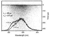
- FIG. 4 is a graph showing PL transient attenuation of an organic photoluminescence device using the compound 18 of Example 1.
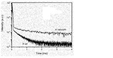
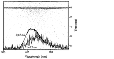
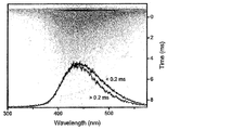
- 2 is a streak image of an organic photoluminescence device using the compound 18 of Example 1.
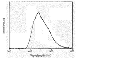
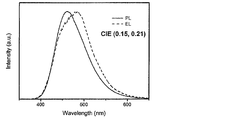
- 2 is an emission spectrum of an organic electroluminescence device using the compound 18 of Example 2.
- 6 is a graph showing current density-voltage-luminance characteristics of an organic electroluminescence device using the compound 18 of Example 2.
- 6 is a graph showing current density-external quantum efficiency characteristics of an organic electroluminescence device using the compound 18 of Example 2.
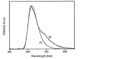
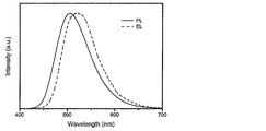
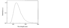
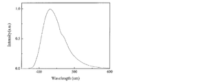
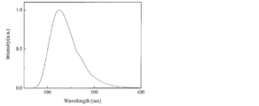
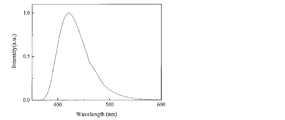
- 2 is an emission spectrum of an organic photoluminescence device using the compound 1 of Example 3.
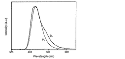
- 3 is an emission spectrum of an organic photoluminescence device using the compound 3 of Example 3.
- 2 is an emission spectrum of an organic photoluminescence device using the compound 21 of Example 3. It is an emission spectrum of the organic photoluminescent element using the compound 22 of Example 3, and the organic electroluminescent element of Example 6.
- 2 is an emission spectrum of an organic photoluminescence device using the compound 355 of Example 3 and an organic electroluminescence device of Example 6.
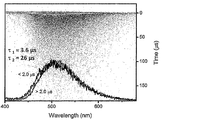
- 3 is a streak image of an organic photoluminescence device using the compound 1 of Example 3.
- 2 is a streak image of an organic photoluminescence device using the compound 3 of Example 3.
- 3 is a streak image of an organic photoluminescence device using the compound 21 of Example 3.
- 3 is a streak image of an organic photoluminescence device using the compound 22 of Example 3.
- FIG. 3 is a streak image of an organic photoluminescence device using the compound 230 of Example 3.
- 3 is a streak image of an organic photoluminescence device using the compound 355 of Example 3.
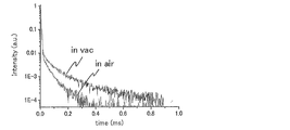
- FIG. 3 shows PL transient attenuation of an organic photoluminescence device using Compound 1, Compound 3 and Compound 21 of Example 3.
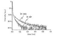
- FIG. 3 shows PL transient attenuation of an organic photoluminescence device using the compound 230 of Example 3.
- FIG. 2 is an emission spectrum of an organic electroluminescence device using the compound 21 of Example 4.
- 6 is a graph showing current density-voltage-luminance characteristics of an organic electroluminescence device using the compound 21 of Example 4.
- 6 is a graph showing current density-external quantum efficiency characteristics of an organic electroluminescence device using the compound 21 of Example 4.
- 6 is a graph showing current density-external quantum efficiency characteristics of an organic electroluminescence device using Compound 1 and Compound 3 of Example 5.
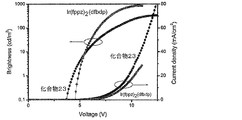
- 6 is a graph showing the current density-external quantum efficiency characteristics of an organic electroluminescence device using the compound 21 of Example 5 and Ir (fppz) 2 (dfbdp).
- 6 is a graph showing current density-voltage-luminance characteristics of an organic electroluminescence device using the compound 21 of Example 5 and Ir (fppz) 2 (dfbdp).
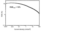
- 6 is a graph showing current density-external quantum efficiency characteristics of an organic electroluminescence device using the compound 22 of Example 6.
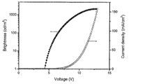
- 6 is a graph showing current density-voltage-luminance characteristics of an organic electroluminescence device using the compound 22 of Example 6.
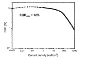
- 10 is a graph showing current density-external quantum efficiency characteristics of an organic electroluminescence device using the compound 355 of Example 7.
- 6 is a graph showing current density-voltage-luminance characteristics of an organic electroluminescence device using the compound 355 of Example 7.
- 6 is an emission spectrum of an organic photoluminescence device using the compound 364 of Example 8.
- 7 is an emission spectrum of an organic photoluminescence device using the compound 367 of Example 8.
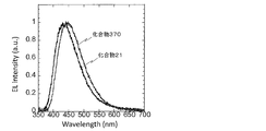
- 10 is an emission spectrum of an organic photoluminescence device using the compound 370 of Example 8.
- 7 is an emission spectrum of an organic photoluminescence device using the compound 373 of Example 8.
- 7 is an emission spectrum of an organic photoluminescence device using the compound 376 of Example 8.
- 10 is a graph showing PL transient attenuation of an organic photoluminescence device using the compound 364 of Example 9. It is a graph which shows PL transient attenuation
- 10 is a graph showing PL transient attenuation of an organic photoluminescence device using the compound 370 of Example 9. It is a graph which shows PL transient attenuation
- 10 is a graph showing PL transient attenuation of an organic photoluminescence device using the compound 376 of Example 9. It is an emission spectrum of the organic electroluminescent element using the compound 21 and the compound 370 of Example 10.
- 6 is a graph showing current density-external quantum efficiency characteristics of an organic electroluminescence device using the compound 21 and the compound 370 of Example 10. It is a graph which shows PL transient attenuation
- 6 is an emission spectrum of an organic photoluminescence device using the compound 453 of Example 12.
- 6 is a streak image of an organic photoluminescence device using the compound 453 of Example 12.
- FIG. It is an emission spectrum of the organic electroluminescent element using the compound 453 of Example 13.
- 14 is a graph showing current density-external quantum efficiency characteristics of an organic electroluminescence device using the compound 453 of Example 13.
- a numerical range represented by using “to” means a range including numerical values described before and after “to” as a lower limit value and an upper limit value.
- the luminescent material of the present invention is characterized by comprising a compound represented by the following general formula (1).
- the organic light-emitting device of the present invention is characterized by containing a compound represented by the following general formula (1) as a light-emitting material of the light-emitting layer. Therefore, first, the compound represented by the general formula (1) will be described.
- R 1 to R 10 each independently represents a hydrogen atom or a substituent. However, not all of R 1 to R 10 are hydrogen atoms.
- the number of substituents is preferably 1 to 8, and more preferably 1 to 6.
- the number of substituents may be 1 to 4, 2 to 6, or 2 to 4.
- the number of substituents may be the same as or different from each other. When they are the same, there is an advantage that synthesis is easy.
- any of R 2 to R 4 and R 7 to R 9 is preferably a substituent, and the other is preferably a hydrogen atom.
- at least one of R 2 to R 4 and R 7 to R 9 preferably two or more are used as a substituent, or at least one of R 2 to R 4 and R 7 to R 9 At least one of them as a substituent, at least one of R 2 , R 4 , R 7 and R 9 , preferably two or more as a substituent, and R 2 and R 4
- R 2 to R 4 and R 7 to R 9 are substituents and the others are hydrogen atoms, or all of R 2 , R 4 , R 7 and R 9 are substituents.
- the other is a hydrogen atom
- R 2 and R 4 are substituents and the other is a hydrogen atom
- R 2 is a substituent and the other is a hydrogen atom
- R 3 is a substituent and the others are hydrogen atoms
- R 1 to R 10 can take include, for example, a hydroxy group, a halogen atom, a cyano group, an alkyl group having 1 to 20 carbon atoms, an alkoxy group having 1 to 20 carbon atoms, an alkylthio group having 1 to 20 carbon atoms, carbon An alkyl-substituted amino group having 1 to 20 carbon atoms, an acyl group having 2 to 20 carbon atoms, an aryl group having 6 to 40 carbon atoms, a heteroaryl group having 3 to 40 carbon atoms, a diarylamino group having 12 to 40 carbon atoms, and a carbon number A substituted or unsubstituted carbazolyl group having 12 to 40 carbon atoms, an alkenyl group having 2 to 10 carbon atoms, an alkynyl group having 2 to 10 carbon atoms, an alkoxycarbonyl group having 2 to 10 carbon atoms, an alkylsulfonyl group having 1 to
- substituents are a halogen atom, a cyano group, a substituted or unsubstituted alkyl group having 1 to 20 carbon atoms, an alkoxy group having 1 to 20 carbon atoms, a substituted or unsubstituted aryl group having 6 to 40 carbon atoms, carbon A substituted or unsubstituted heteroaryl group having 3 to 40 carbon atoms, a substituted or unsubstituted diarylamino group having 12 to 40 carbon atoms, and a substituted or unsubstituted carbazolyl group having 12 to 40 carbon atoms.
- substituents are a fluorine atom, a chlorine atom, a cyano group, a substituted or unsubstituted alkyl group having 1 to 10 carbon atoms, a substituted or unsubstituted alkoxy group having 1 to 10 carbon atoms, and a substituted group having 1 to 10 carbon atoms.
- an unsubstituted dialkylamino group, a substituted or unsubstituted aryl group having 6 to 15 carbon atoms, and a substituted or unsubstituted heteroaryl group having 3 to 12 carbon atoms For example, it can be selected from a substituted or unsubstituted alkyl group having 1 to 6 carbon atoms and a substituted or unsubstituted alkoxy group having 1 to 6 carbon atoms.
- the alkyl group in the present specification may be linear, branched or cyclic, and more preferably has 1 to 6 carbon atoms. Specific examples thereof include a methyl group, an ethyl group, a propyl group, and butyl. Group, t-butyl group, pentyl group, hexyl group and isopropyl group.
- the alkoxy group may be linear, branched or cyclic, and more preferably has 1 to 6 carbon atoms, and specific examples include methoxy group, ethoxy group, propoxy group, butoxy group, t-butoxy group. A group, a pentyloxy group, a hexyloxy group, and an isopropyloxy group.
- the two alkyl groups of the dialkylamino group may be the same or different from each other, but are preferably the same.
- the two alkyl groups of the dialkylamino group may each independently be linear, branched or cyclic, and more preferably have 1 to 6 carbon atoms. Specific examples include a methyl group, an ethyl group, Examples thereof include a propyl group, a butyl group, a pentyl group, a hexyl group, and an isopropyl group.
- the aryl group may be a single ring or a fused ring, and specific examples thereof include a phenyl group and a naphthyl group.
- the heteroaryl group may be a monocyclic ring or a fused ring, and specific examples include a pyridyl group, a pyridazyl group, a pyrimidyl group, a triazyl group, a triazolyl group, and a benzotriazolyl group.
- These heteroaryl groups may be a group bonded through a hetero atom or a group bonded through a carbon atom constituting a heteroaryl ring.
- R 1 and R 2 , R 2 and R 3 , R 3 and R 4 , R 4 and R 5 , R 5 and R 6 , R 6 and R 7 , R 7 and R 8 , R 8 and R 9 , and R 9 and R 10 may be bonded to each other to form a cyclic structure. Only one of these may form a cyclic structure, or two or more may form a cyclic structure. When a cyclic structure is formed, the cyclic structure is any one of R 2 and R 3 , R 3 and R 4 , R 5 and R 6 , R 7 and R 8 , R 8 and R 9. It is preferable to be formed as described above.
- R 5 and R 6 When R 5 and R 6 are bonded to each other, it is preferably a single bond or a connecting group having 1 or 2 connecting chain constituent atoms to form a 5- to 7-membered ring, respectively.
- Examples of the connecting group having 1 or 2 connecting chain constituent atoms include a methylene group, an ethylene group, and an ethenylene group.
- the cyclic structure formed by bonding R 2 and R 3 , R 3 and R 4 , R 7 and R 8 , R 8 and R 9 may include a hetero atom in the ring skeleton.
- the hetero atom here is preferably selected from the group consisting of a nitrogen atom, an oxygen atom and a sulfur atom.
- Examples of cyclic structures formed include benzene ring, naphthalene ring, pyridine ring, pyridazine ring, pyrimidine ring, pyrazine ring, pyrrole ring, imidazole ring, pyrazole ring, triazole ring, imidazoline ring, oxazole ring, isoxazole ring, thiazole Ring, isothiazole ring, cyclohexadiene ring, cyclohexene ring, cyclopentaene ring, cycloheptatriene ring, cycloheptadiene ring, cycloheptaene ring and the like, and a benzene ring, a pyridine ring, and a cyclohexene ring are more preferable. .
- the formed cyclic structure may be a fused ring.
- At least one of R 1 to R 10 is a substituted or unsubstituted aryl group, a substituted or unsubstituted diarylamino group, or a substituted or unsubstituted 9-carbazolyl group.
- Preferred is an embodiment in which at least one of R 1 to R 10 is a substituted or unsubstituted diarylamino group, or a substituted or unsubstituted 9-carbazolyl group.
- a substituted or unsubstituted diarylamino group and a substituted or unsubstituted 9-carbazolyl group may be mixed, and a substituted or unsubstituted aryl group, substituted or unsubstituted
- a substituted diarylamino group may be mixed, a substituted or unsubstituted aryl group and a substituted or unsubstituted 9-carbazolyl group may be mixed, a substituted or unsubstituted aryl group,
- Three types of an unsubstituted diarylamino group and a substituted or unsubstituted 9-carbazolyl group may be mixed.
- the two aryl groups of the diarylamino group referred to here may be linked to each other by a linking group.
- At least one of R 1 to R 10 is preferably a group having a structure represented by the following general formula (6).
- R 11 to R 20 each independently represents a hydrogen atom or a substituent.
- R 15 and R 16 may be bonded to each other to form a single bond or a divalent linking group.
- the divalent linking group include —O—, —S—, —N (R) — and the like. Of these, —O— and —S— are preferable.
- R in —N (R) — represents a substituted or unsubstituted alkyl group or a substituted or unsubstituted aryl group, preferably a substituted or unsubstituted alkyl group having 1 to 10 carbon atoms, or 6 to 14 carbon atoms.
- a substituted or unsubstituted aryl group more preferably a substituted or unsubstituted alkyl group having 1 to 6 carbon atoms, a substituted or unsubstituted aryl group having 6 to 10 carbon atoms, and still more preferably a carbon number 1 to 3 substituted or unsubstituted alkyl groups.
- R 11 and R 12 , R 12 and R 13 , R 13 and R 14 , R 14 and R 15 , R 16 and R 17 , R 17 and R 18 , R 18 and R 19 , R 19 and R 20 are respectively They may be bonded together to form a ring structure.
- R 11 to R 20 in the general formula (6) refer to the explanations and preferred ranges of the substituents and cyclic structures in the general formula (1). it can.
- At least one of R 1 to R 10 in the general formula (1) is preferably a group having a structure represented by the following general formula (7).
- R 21 to R 30 each independently represents a hydrogen atom or a substituent.
- R 21 and R 22 , R 22 and R 23 , R 23 and R 24 , R 24 and R 25 , R 26 and R 27 , R 27 and R 28 , R 28 and R 29 , R 29 and R 30 are respectively They may be bonded together to form a ring structure.
- R 21 to R 20 in general formula (7) refer to the explanation and preferred ranges of substituents and cyclic structures in general formula (1) above. it can.
- At least one of R 1 to R 10 in the general formula (1) is preferably a group having a structure represented by the following general formula (8).
- R 31 to R 34 and R 37 to R 40 each independently represents a hydrogen atom or a substituent.
- R 31 and R 32 , R 32 and R 33 , R 33 and R 34 , R 37 and R 38 , R 38 and R 39 , and R 39 and R 40 may be bonded to each other to form a cyclic structure.
- the explanations and preferred ranges of the substituents and cyclic structures that can be taken by R 31 to R 34 and R 37 to R 40 in the general formula (8) the explanations and preferred ranges of the substituents and the cyclic structures in the general formula (1) are preferable. You can refer to the range.
- At least one of R 1 to R 10 in the general formula (1) is preferably a group having a structure represented by the following general formula (9).
- R 41 to R 50 each independently represents a hydrogen atom or a substituent.
- R 41 and R 42 , R 42 and R 43 , R 43 and R 44 , R 47 and R 48 , R 48 and R 49 , R 49 and R 50 may be bonded to each other to form a cyclic structure.
- R 41 to R 50 refer to the explanations and preferred ranges of the substituents and cyclic structures in the general formula (1). it can.
- R 45 and R 46 in the general formula (9) can take are a substituted or unsubstituted alkyl group and a substituted or unsubstituted aryl group.
- a substituted or unsubstituted alkyl group is preferable.
- the alkyl group preferably has 1 to 15 carbon atoms, more preferably 1 to 10 carbon atoms, and still more preferably 1 to 6 carbon atoms.
- R 1 - R 10 is has a structure represented by any one of the above general formula (7) to (9), the other of R 1 - R 10
- An embodiment in which at least one has another structure represented by the general formulas (7) to (9) can also be mentioned as a preferred embodiment.
- the compound represented by the general formula (1) preferably has a structure represented by the following general formula (2).
- R 1 , R 2 , R 4 to R 7 , R 9 , and R 10 each independently represent a hydrogen atom or a substituent.
- Z 3 and Z 8 each independently represent a hydrogen atom, a substituted or unsubstituted aryl group, a substituted or unsubstituted diarylamino group, or a substituted or unsubstituted 9-carbazolyl group, both of which are hydrogen atoms There is nothing.
- Z 3 and Z 4 are preferably each independently a substituted or unsubstituted diarylamino group, or a substituted or unsubstituted 9-carbazolyl group, represented by the above general formula (7) or general formula (8).
- R 1 and R 2 , R 4 and R 5 , R 5 and R 6 , R 6 and R 7 , and R 9 and R 10 may be bonded to each other to form a cyclic structure.
- R 1 , R 2 , R 4 to R 7 , R 9 , R 10 are preferably each independently a hydrogen atom, a substituted or unsubstituted alkyl group, or a substituted or unsubstituted alkoxy group, and all hydrogen atoms It is also preferable.
- the compound represented by the general formula (1) preferably has a structure represented by the following general formula (3).
- R 1 , R 3 , R 5 to R 7 , R 9 , and R 10 each independently represent a hydrogen atom or a substituent.
- Z 2, Z 4 and Z 8 are each independently a hydrogen atom, a substituted or unsubstituted aryl group, a substituted or unsubstituted diarylamino group or a substituted or unsubstituted 9-carbazolyl group, all hydrogen atoms Never.
- Z 2 , Z 4 and Z 8 are preferably each independently a substituted or unsubstituted diarylamino group, or a substituted or unsubstituted 9-carbazolyl group.
- R 5 and R 6 , R 6 and R 7 , R 9 and R 10 may be bonded to each other to form a cyclic structure.
- R 1 , R 3 , R 5 to R 7 , R 9 and R 10 are each independently preferably a hydrogen atom, a substituted or unsubstituted alkyl group, or a substituted or unsubstituted alkoxy group, and all are hydrogen atoms. It is also preferable.
- the compound represented by the general formula (1) has a structure represented by the following general formula (4).
- R 1 , R 3 , R 5 , R 6 , R 8 and R 10 each independently represent a hydrogen atom or a substituent.
- R 5 and R 6 may combine with each other to form a cyclic structure.
- Z 2 , Z 4 , Z 7 and Z 9 each independently represent a hydrogen atom, a substituted or unsubstituted aryl group, a substituted or unsubstituted diarylamino group, or a substituted or unsubstituted 9-carbazolyl group, substituted or An unsubstituted diarylamino group or a substituted or unsubstituted 9-carbazolyl group is preferable, and a group represented by the general formula (7) or the general formula (8) is more preferable.
- Z 2 , Z 4 , Z 7 and Z 9 are hydrogen atoms.
- R 1 , R 3 , R 5 , R 6 , R 8 and R 10 are each independently preferably a hydrogen atom, a substituted or unsubstituted alkyl group, or a substituted or unsubstituted alkoxy group, and all are hydrogen atoms. It is also preferable.
- the compound represented by the general formula (1) has a structure represented by the following general formula (5).
- R 2 , R 3 , R 4 , R 5 , R 6 , R 7 , R 8 , R 9 each independently represents a hydrogen atom or a substituent.
- R 2 and R 3 , R 3 and R 4 , R 4 and R 5 , R 5 and R 6 , R 6 and R 7 , R 7 and R 8 , R 8 and R 9 are bonded to each other to form a cyclic structure May be formed.
- Z 1 and Z 10 each independently represents a hydrogen atom, a substituted or unsubstituted aryl group, a substituted or unsubstituted diarylamino group, or a substituted or unsubstituted 9-carbazolyl group, and a substituted or unsubstituted diarylamino group Or a substituted or unsubstituted 9-carbazolyl group, more preferably a group represented by the above general formula (7) or general formula (8).
- Z 1 and Z 10 are not both hydrogen atoms.
- R 2 , R 3 , R 4 , R 5 , R 6 , R 7 , R 8 and R 9 are each independently a hydrogen atom, a substituted or unsubstituted alkyl group, or a substituted or unsubstituted alkoxy group. It is also preferable that all are hydrogen atoms.
- the molecular weight of the compound represented by the general formula (1) is, for example, 1500 or less when the organic layer containing the compound represented by the general formula (1) is intended to be formed by vapor deposition. Preferably, it is preferably 1200 or less, more preferably 1000 or less, and even more preferably 800 or less. The lower limit of the molecular weight is the molecular weight of the compound 101.
- the compound represented by the general formula (1) may be formed by a coating method regardless of the molecular weight. If a coating method is used, a film can be formed even with a compound having a relatively large molecular weight.
- a compound containing a plurality of structures represented by the general formula (1) in the molecule may be used for the light emitting layer of the organic light emitting device.
- a polymer obtained by polymerizing a polymerizable monomer having a structure represented by the general formula (1) for a light emitting layer of an organic light emitting device.
- a monomer having a polymerizable functional group in any one of R 1 to R 10 of the general formula (1) and polymerizing it alone or copolymerizing with other monomers, It is considered that a polymer having a repeating unit is obtained and the polymer is used for a light emitting layer of an organic light emitting device.
- dimers and trimers are obtained by coupling compounds having a structure represented by the general formula (1) and used in the light emitting layer of the organic light emitting device.
- any one of R 1 to R 10 in the general formula (1) is represented by the following general formula (10) or (11). The thing which is a structure represented can be mentioned.
- L 1 and L 2 each represent a linking group.
- the linking group preferably has 0 to 20 carbon atoms, more preferably 1 to 15 carbon atoms, and still more preferably 2 to 10 carbon atoms. And preferably has a structure represented by - linking group -X 11 -L 11.
- X 11 represents an oxygen atom or a sulfur atom, and is preferably an oxygen atom.
- L 11 represents a linking group, and is preferably a substituted or unsubstituted alkylene group, or a substituted or unsubstituted arylene group, and is a substituted or unsubstituted alkylene group having 1 to 10 carbon atoms, or a substituted or unsubstituted group A phenylene group is more preferable.
- R 101 , R 102 , R 103 and R 104 each independently represent a substituent.
- it is a substituted or unsubstituted alkyl group having 1 to 6 carbon atoms, a substituted or unsubstituted alkoxy group having 1 to 6 carbon atoms, or a halogen atom, more preferably an unsubstituted alkyl group having 1 to 3 carbon atoms.
- An unsubstituted alkoxy group having 1 to 3 carbon atoms, a fluorine atom, and a chlorine atom and more preferably an unsubstituted alkyl group having 1 to 3 carbon atoms and an unsubstituted alkoxy group having 1 to 3 carbon atoms.
- R 1 to R 10 in the general formula (1) is represented by the following formulas (12) to (15).
- R 1 to R 10 may be represented by the following formulas (12) to (15), but preferably one of R 1 to R 10 is represented by the following formulas (12) to (15 ).
- At least one of R 1 to R 10 in the general formula (1) is made into a hydroxy group, and the following compounds are reacted using it as a linker. It can be synthesized by introducing a polymerizable group and polymerizing the polymerizable group.
- the polymer containing the structure represented by the general formula (1) in the molecule may be a polymer composed only of repeating units having the structure represented by the general formula (1), or other structures may be used. It may be a polymer containing repeating units.
- the repeating unit having a structure represented by the general formula (1) contained in the polymer may be a single type or two or more types. Examples of the repeating unit not having the structure represented by the general formula (1) include those derived from monomers used in ordinary copolymerization. Examples thereof include a repeating unit derived from a monomer having an ethylenically unsaturated bond such as ethylene and styrene.
- the method for synthesizing the compound represented by the general formula (1) is not particularly limited.
- the synthesis of the compound represented by the general formula (1) can be performed by appropriately combining known synthesis methods and conditions. For example, it can be synthesized by reacting bis (halogenated phenyl) sulfone with diphenylamine. At this time, for example, the reaction can proceed by heating in the presence of NaH.
- a compound of the general formula (1) having a desired substituent can be synthesized.
- the compound represented by the general formula (1) is preferably a thermally activated delayed fluorescent material.
- a delayed fluorescent material When used as a delayed fluorescent material in the light emitting layer of an organic electroluminescence element, high luminous efficiency can be achieved at a lower cost than in the past.
- a phosphorescent material it is necessary to use a rare metal such as Ir or Pt. If the delayed fluorescent material is used, such an expensive material is not required, and therefore, an organic electroluminescence element having high luminous efficiency can be provided at low cost.
- the compound represented by the general formula (1) of the present invention is useful as a light emitting material of an organic light emitting device. For this reason, the compound represented by General formula (1) of this invention can be effectively used as a luminescent material for the light emitting layer of an organic light emitting element.
- the compound represented by the general formula (1) includes a delayed fluorescent material (delayed phosphor) that emits delayed fluorescence. That is, the present invention relates to a delayed phosphor having a structure represented by the general formula (1), an invention using a compound represented by the general formula (1) as a delayed phosphor, and a general formula (1).
- An invention of a method for emitting delayed fluorescence using the represented compound is also provided.
- An organic light emitting device using such a compound as a light emitting material emits delayed fluorescence and has a feature of high luminous efficiency. The principle will be described below by taking an organic electroluminescence element as an example.
- the organic electroluminescence element carriers are injected into the light emitting material from both positive and negative electrodes to generate an excited light emitting material and emit light.
- 25% of the generated excitons are excited to the excited singlet state, and the remaining 75% are excited to the excited triplet state. Therefore, the use efficiency of energy is higher when phosphorescence, which is light emission from an excited triplet state, is used.
- the excited triplet state has a long lifetime, energy saturation occurs due to saturation of the excited state and interaction with excitons in the excited triplet state, and in general, the quantum yield of phosphorescence is often not high.
- delayed fluorescent materials after energy transition to an excited triplet state due to intersystem crossing, etc., are then crossed back to an excited singlet state due to triplet-triplet annihilation or absorption of thermal energy, and emit fluorescence.
- a thermally activated delayed fluorescent material by absorption of thermal energy is particularly useful.
- excitons in the excited singlet state emit fluorescence as usual.
- excitons in the excited triplet state absorb heat generated by the device and cross between the excited singlets to emit fluorescence.
- the light is emitted from the excited singlet, the light is emitted at the same wavelength as the fluorescence, but the lifetime of light generated (emission life) due to the reverse intersystem crossing from the excited triplet state to the excited singlet state is normal. Since the fluorescence becomes longer than the fluorescence and phosphorescence, it is observed as fluorescence delayed from these. This can be defined as delayed fluorescence. If such a heat-activated exciton transfer mechanism is used, the ratio of the compound in an excited singlet state, which normally generated only 25%, is increased to 25% or more by absorbing thermal energy after carrier injection. It can be raised.
- the heat of the device will sufficiently cause intersystem crossing from the excited triplet state to the excited singlet state and emit delayed fluorescence. Efficiency can be improved dramatically.
- organic light-emitting devices such as an organic photoluminescence device (organic PL device) and an organic electroluminescence device (organic EL device) can be provided.
- the organic photoluminescence element has a structure in which at least a light emitting layer is formed on a substrate.
- the organic electroluminescence element has a structure in which an organic layer is formed at least between an anode, a cathode, and an anode and a cathode.
- the organic layer includes at least a light emitting layer, and may consist of only the light emitting layer, or may have one or more organic layers in addition to the light emitting layer.
- Examples of such other organic layers include a hole transport layer, a hole injection layer, an electron blocking layer, a hole blocking layer, an electron injection layer, an electron transport layer, and an exciton blocking layer.
- the hole transport layer may be a hole injection / transport layer having a hole injection function
- the electron transport layer may be an electron injection / transport layer having an electron injection function.
- FIG. 1 A specific example of the structure of an organic electroluminescence element is shown in FIG. In FIG. 1, 1 is a substrate, 2 is an anode, 3 is a hole injection layer, 4 is a hole transport layer, 5 is a light emitting layer, 6 is an electron transport layer, and 7 is a cathode. Below, each member and each layer of an organic electroluminescent element are demonstrated. In addition, description of a board
- the organic electroluminescence device of the present invention is preferably supported on a substrate.
- the substrate is not particularly limited and may be any substrate conventionally used for organic electroluminescence elements.
- a substrate made of glass, transparent plastic, quartz, silicon, or the like can be used.
- an electrode material made of a metal, an alloy, an electrically conductive compound, or a mixture thereof having a high work function (4 eV or more) is preferably used.
- electrode materials include metals such as Au, and conductive transparent materials such as CuI, indium tin oxide (ITO), SnO 2 and ZnO.
- conductive transparent materials such as CuI, indium tin oxide (ITO), SnO 2 and ZnO.
- an amorphous material such as IDIXO (In 2 O 3 —ZnO) capable of forming a transparent conductive film may be used.
- a thin film may be formed by vapor deposition or sputtering of these electrode materials, and a pattern of a desired shape may be formed by photolithography, or when pattern accuracy is not so high (about 100 ⁇ m or more) ), A pattern may be formed through a mask having a desired shape at the time of vapor deposition or sputtering of the electrode material.
- wet film-forming methods such as a printing system and a coating system, can also be used.
- the transmittance be greater than 10%, and the sheet resistance as the anode is preferably several hundred ⁇ / ⁇ or less.
- the film thickness depends on the material, it is usually selected in the range of 10 to 1000 nm, preferably 10 to 200 nm.
- cathode a material having a low work function (4 eV or less) metal (referred to as an electron injecting metal), an alloy, an electrically conductive compound, and a mixture thereof as an electrode material is used.
- electrode materials include sodium, sodium-potassium alloy, magnesium, lithium, magnesium / copper mixture, magnesium / silver mixture, magnesium / aluminum mixture, magnesium / indium mixture, aluminum / aluminum oxide (Al 2 O 3 ) Mixtures, indium, lithium / aluminum mixtures, rare earth metals and the like.
- a mixture of an electron injecting metal and a second metal which is a stable metal having a larger work function value than this for example, a magnesium / silver mixture, Magnesium / aluminum mixtures, magnesium / indium mixtures, aluminum / aluminum oxide (Al 2 O 3 ) mixtures, lithium / aluminum mixtures, aluminum and the like are preferred.
- the cathode can be produced by forming a thin film of these electrode materials by a method such as vapor deposition or sputtering.
- the sheet resistance as the cathode is preferably several hundred ⁇ / ⁇ or less, and the film thickness is usually selected in the range of 10 nm to 5 ⁇ m, preferably 50 to 200 nm.
- the emission luminance is advantageously improved.
- a transparent or semi-transparent cathode can be produced. By applying this, an element in which both the anode and the cathode are transparent is used. Can be produced.
- the light emitting layer is a layer that emits light after excitons are generated by recombination of holes and electrons injected from each of the anode and the cathode, and the light emitting material may be used alone for the light emitting layer. , Preferably including a luminescent material and a host material.
- a luminescent material the 1 type (s) or 2 or more types chosen from the compound group of this invention represented by General formula (1) can be used.
- a host material in addition to the light emitting material in the light emitting layer.
- the host material an organic compound having at least one of excited singlet energy and excited triplet energy higher than that of the light emitting material of the present invention can be used.
- singlet excitons and triplet excitons generated in the light emitting material of the present invention can be confined in the molecules of the light emitting material of the present invention, and the light emission efficiency can be sufficiently extracted.
- high luminous efficiency can be obtained, so that host materials that can achieve high luminous efficiency are particularly limited. And can be used in the present invention.
- the organic light emitting device or organic electroluminescent device of the present invention light emission is generated from the light emitting material of the present invention contained in the light emitting layer. This emission includes both fluorescence and delayed fluorescence. However, light emission from the host material may be partly or partly emitted.
- the amount of the compound of the present invention, which is a light emitting material is preferably 0.1% by weight or more, more preferably 1% by weight or more, and 50% or more. It is preferably no greater than wt%, more preferably no greater than 20 wt%, and even more preferably no greater than 10 wt%.
- the host material in the light-emitting layer is preferably an organic compound that has a hole transporting ability and an electron transporting ability, prevents the emission of longer wavelengths, and has a high glass transition temperature.
- the injection layer is a layer provided between the electrode and the organic layer for lowering the driving voltage and improving the luminance of light emission.
- the injection layer can be provided as necessary.
- the blocking layer is a layer that can prevent diffusion of charges (electrons or holes) and / or excitons existing in the light emitting layer to the outside of the light emitting layer.
- the electron blocking layer can be disposed between the light emitting layer and the hole transport layer and blocks electrons from passing through the light emitting layer toward the hole transport layer.
- a hole blocking layer can be disposed between the light emitting layer and the electron transporting layer to prevent holes from passing through the light emitting layer toward the electron transporting layer.
- the blocking layer can also be used to block excitons from diffusing outside the light emitting layer. That is, each of the electron blocking layer and the hole blocking layer can also function as an exciton blocking layer.
- the term “electron blocking layer” or “exciton blocking layer” as used herein is used in the sense of including a layer having the functions of an electron blocking layer and an exciton blocking layer in one layer.
- the hole blocking layer has a function of an electron transport layer in a broad sense.
- the hole blocking layer has a role of blocking holes from reaching the electron transport layer while transporting electrons, thereby improving the recombination probability of electrons and holes in the light emitting layer.
- the material for the hole blocking layer the material for the electron transport layer described later can be used as necessary.
- the electron blocking layer has a function of transporting holes in a broad sense.
- the electron blocking layer has a role to block electrons from reaching the hole transport layer while transporting holes, thereby improving the probability of recombination of electrons and holes in the light emitting layer. .
- the exciton blocking layer is a layer for preventing excitons generated by recombination of holes and electrons in the light emitting layer from diffusing into the charge transport layer. It becomes possible to efficiently confine in the light emitting layer, and the light emission efficiency of the device can be improved.
- the exciton blocking layer can be inserted on either the anode side or the cathode side adjacent to the light emitting layer, or both can be inserted simultaneously.
- the layer when the exciton blocking layer is provided on the anode side, the layer can be inserted adjacent to the light emitting layer between the hole transport layer and the light emitting layer, and when inserted on the cathode side, the light emitting layer and the cathode Between the luminescent layer and the light-emitting layer.
- a hole injection layer, an electron blocking layer, or the like can be provided between the anode and the exciton blocking layer adjacent to the anode side of the light emitting layer, and the excitation adjacent to the cathode and the cathode side of the light emitting layer can be provided.
- an electron injection layer, an electron transport layer, a hole blocking layer, and the like can be provided.
- the blocking layer is disposed, at least one of the excited singlet energy and the excited triplet energy of the material used as the blocking layer is preferably higher than the excited singlet energy and the excited triplet energy of the light emitting material.
- the hole transport layer is made of a hole transport material having a function of transporting holes, and the hole transport layer can be provided as a single layer or a plurality of layers.
- the hole transport material has any one of hole injection or transport and electron barrier properties, and may be either organic or inorganic.
- hole transport materials that can be used include, for example, triazole derivatives, oxadiazole derivatives, imidazole derivatives, carbazole derivatives, indolocarbazole derivatives, polyarylalkane derivatives, pyrazoline derivatives and pyrazolone derivatives, phenylenediamine derivatives, arylamine derivatives, Examples include amino-substituted chalcone derivatives, oxazole derivatives, styrylanthracene derivatives, fluorenone derivatives, hydrazone derivatives, stilbene derivatives, silazane derivatives, aniline copolymers, and conductive polymer oligomers, particularly thiophene oligomers.
- An aromatic tertiary amine compound and an styrylamine compound are preferably used, and an aromatic tertiary amine compound is more preferably used.
- the electron transport layer is made of a material having a function of transporting electrons, and the electron transport layer can be provided as a single layer or a plurality of layers.
- the electron transport material (which may also serve as a hole blocking material) may have a function of transmitting electrons injected from the cathode to the light emitting layer.
- Examples of the electron transport layer that can be used include nitro-substituted fluorene derivatives, diphenylquinone derivatives, thiopyran dioxide oxide derivatives, carbodiimides, fluorenylidenemethane derivatives, anthraquinodimethane and anthrone derivatives, oxadiazole derivatives, and the like.
- a thiadiazole derivative in which the oxygen atom of the oxadiazole ring is substituted with a sulfur atom, and a quinoxaline derivative having a quinoxaline ring known as an electron withdrawing group can also be used as an electron transport material.
- a polymer material in which these materials are introduced into a polymer chain or these materials are used as a polymer main chain can also be used.
- the compound represented by the general formula (1) may be used not only for the light emitting layer but also for layers other than the light emitting layer.
- the compound represented by General formula (1) used for a light emitting layer and the compound represented by General formula (1) used for layers other than a light emitting layer may be same or different.
- the compound represented by the general formula (1) may be used for the injection layer, blocking layer, hole blocking layer, electron blocking layer, exciton blocking layer, hole transporting layer, electron transporting layer, and the like. .
- the method for forming these layers is not particularly limited, and the layer may be formed by either a dry process or a wet process.
- the preferable material which can be used for an organic electroluminescent element is illustrated concretely.
- the material that can be used in the present invention is not limited to the following exemplary compounds.
- R, R ′, and R 1 to R 10 in the structural formulas of the following exemplary compounds each independently represent a hydrogen atom or a substituent.
- X represents a carbon atom or a hetero atom forming a ring skeleton
- n represents an integer of 3 to 5
- Y represents a substituent
- m represents an integer of 0 or more.
- the organic electroluminescence device produced by the above-described method emits light by applying an electric field between the anode and the cathode of the obtained device. At this time, if the light is emitted by excited singlet energy, light having a wavelength corresponding to the energy level is confirmed as fluorescence emission and delayed fluorescence emission. In addition, in the case of light emission by excited triplet energy, a wavelength corresponding to the energy level is confirmed as phosphorescence. Since normal fluorescence has a shorter fluorescence lifetime than delayed fluorescence, the emission lifetime can be distinguished from fluorescence and delayed fluorescence.
- the excited triplet energy is unstable and is converted into heat and the like, and the lifetime is short and it is immediately deactivated.
- the excited triplet energy of a normal organic compound it can be measured by observing light emission under extremely low temperature conditions.
- the organic electroluminescence element of the present invention can be applied to any of a single element, an element having a structure arranged in an array, and a structure in which an anode and a cathode are arranged in an XY matrix. According to the present invention, an organic light emitting device with greatly improved light emission efficiency can be obtained by containing the compound represented by the general formula (1) in the light emitting layer.
- the organic light emitting device such as the organic electroluminescence device of the present invention can be further applied to various uses. For example, it is possible to produce an organic electroluminescence display device using the organic electroluminescence element of the present invention.
- organic electroluminescence device of the present invention can be applied to organic electroluminescence illumination and backlights that are in great demand.
- Example 1 an organic photoluminescence device having a light-emitting layer composed of the compound 18 and a host material was produced, and the characteristics were evaluated.
- Compound 18 and DPEPO were deposited from different deposition sources on a silicon substrate by vacuum deposition under a vacuum degree of 5.0 ⁇ 10 ⁇ 4 Pa, and a thin film having a concentration of compound 18 of 10% by weight was formed to 100 nm.
- An organic photoluminescence device was formed with a thickness of 1 mm.
- a C9920-02 type absolute quantum yield measuring device manufactured by Hamamatsu Photonics Co., Ltd. the emission spectrum from the thin film when irradiated with light of 337 nm with an N 2 laser was characterized at 300K.
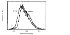
- FIG. 3 shows streak images of fluorescence and delayed fluorescence.
- Example 2 an organic electroluminescence device having a light-emitting layer composed of the compound 18 and a host material was produced, and the characteristics were evaluated.
- Each thin film was laminated at a vacuum degree of 5.0 ⁇ 10 ⁇ 4 Pa by a vacuum deposition method on a glass substrate on which an anode made of indium tin oxide (ITO) having a thickness of 100 nm was formed.
- ITO indium tin oxide
- ⁇ -NPD was formed on ITO to a thickness of 40 nm, and mCP was formed thereon to a thickness of 10 nm.
- Compound 18 and DPEPO were co-evaporated from different vapor deposition sources to form a 20 nm thick layer to be a light emitting layer.
- the concentration of the compound 18 was 6.0% by weight.
- DPEPO was formed to a thickness of 10 nm, and TPBI was formed thereon to a thickness of 30 nm.
- lithium fluoride (LiF) was vacuum-deposited by 0.5 nm, and then aluminum (Al) was vapor-deposited to a thickness of 80 nm to form a cathode, whereby an organic electroluminescence element was obtained.
- a semiconductor parameter analyzer manufactured by Agilent Technologies: E5273A
- an optical power meter measuring device manufactured by Newport: 1930C
- an optical spectrometer manufactured by Ocean Optics: USB2000
- the emission spectrum is shown in FIG. 4, the current density-voltage-luminance characteristic is shown in FIG. 5, and the current density-external quantum efficiency characteristic is shown in FIG.
- the organic electroluminescence device using Compound 18 as the light emitting material achieved an external quantum efficiency of 3.2%.
- Example 3 An organic photoluminescence device was produced using Compound 1, Compound 3, Compound 21, Compound 22, Compound 230, and Compound 355 instead of Compound 18 of Example 1, and the characteristics were evaluated. As a result, delayed fluorescence with a long emission lifetime was observed in addition to fluorescence with a short emission lifetime. 7 to 11 show emission spectra. 12 to 17 show streak images, and FIGS. 18 and 19 show PL transient attenuation.
- Example 4 An organic electroluminescence device was produced using the compound 21 instead of the compound 18 of Example 1, and the characteristics were evaluated.
- the emission spectrum is shown in FIG. 20, the current density-voltage-luminance characteristic is shown in FIG. 21, and the current density-external quantum efficiency characteristic is shown in FIG.
- the organic electroluminescence device using Compound 24 as the light emitting material achieved a high external quantum efficiency of 6.7%.
- Example 5 an organic electroluminescence device having a light emitting layer composed of Compound 1 and a host material was produced. Each thin film was laminated at a vacuum degree of 5.0 ⁇ 10 ⁇ 4 Pa by a vacuum deposition method on a glass substrate on which an anode made of indium tin oxide (ITO) having a thickness of 100 nm was formed. First, ⁇ -NPD is formed on ITO with a thickness of 30 nm, and TCTA (4, 4 ′ , 4 ′′ -tris (N-carbazolyl) -triphenylamine) is formed thereon with a thickness of 20 nm.
- ITO indium tin oxide
- CzSi was formed thereon to a thickness of 10 nm, and then Compound 1 and DPEPO were co-evaporated from different evaporation sources to form a 20 nm thick layer as a light emitting layer.
- DPEPO was formed to a thickness of 10 nm
- TPBI was formed to a thickness of 30 nm
- lithium fluoride (LiF) was vacuum-deposited to a thickness of 0.5 nm.
- Al aluminum
- An organic electroluminescence device was produced in the same manner using Compound 3, Compound 21 and Ir (fppz) 2 (dfbdp) instead of Compound 1. About each produced organic electroluminescent element, it measured by the same method as Example 2.
- FIG. 23 and 24 show the current density-external quantum efficiency characteristics.
- FIG. 25 shows current density-voltage-luminance characteristics.
- Example 6 An organic electroluminescence device was prepared in the same manner as in Example 5 except that Compound 22 (10.0% by weight) was used instead of Compound 1 (6.0% by weight) of Example 5, and the characteristics were similarly obtained. evaluated.
- FIG. 10 shows an emission spectrum
- FIG. 26 shows current density-external quantum efficiency characteristics
- FIG. 27 shows current density-voltage-luminance characteristics.
- Example 7 an organic electroluminescence element having a light-emitting layer made of the compound 355 and a host material was fabricated and the characteristics were evaluated. Each thin film was laminated at a vacuum degree of 5.0 ⁇ 10 ⁇ 4 Pa by a vacuum deposition method on a glass substrate on which an anode made of indium tin oxide (ITO) having a thickness of 100 nm was formed. First, ⁇ -NPD was formed on ITO to a thickness of 40 nm, and then compound 355 and CBP were co-deposited from different evaporation sources to form a 20 nm-thick layer as a light emitting layer. At this time, the concentration of the compound 355 was 10.0% by weight.
- ITO indium tin oxide
- TPBI is formed to a thickness of 60 nm
- further lithium fluoride (LiF) is vacuum-deposited to 0.5 nm
- aluminum (Al) is evaporated to a thickness of 80 nm to form a cathode.
- FIG. 11 shows an emission spectrum
- current density-external quantum efficiency characteristics are shown in FIG. 28, and current density-voltage-luminance characteristics are shown in FIG.
- Example 8 In this example, a toluene solution (concentration 10 ⁇ 5 mol / L) of each of the compounds 364, 367, 370, 373, and 376 was prepared, and the fluorescence spectrum was measured. The results are shown in order in FIGS.
- Example 9 an organic photoluminescence element having a light-emitting layer composed of each compound of Compound 364, Compound 367, Compound 370, Compound 373, and Compound 376 and a host material was fabricated, and the characteristics were evaluated.
- the specific procedure was the same as in Example 1, and the compound 364, compound 367, compound 370, compound 373 and compound 376 were used in place of the compound 18 of Example 1.
- the concentration of each compound was 6% by weight.
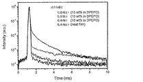
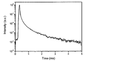
- delayed fluorescence having a long emission lifetime was observed in addition to fluorescence having a short emission lifetime. Time-resolved spectra obtained in the same manner as in Example 1 are shown in FIGS.
- ⁇ E ST of compound 364, compound 367, and compound 370 energy difference between the lowest excited triplet energy level at 77 ° K and the lowest excited singlet energy level in the light emitting material emitting light at the shortest wavelength
- delayed fluorescence component The following table shows the lifetime ( ⁇ DLAYED ), emission quantum efficiency (PLQE), emission fluorescence efficiency of ordinary fluorescent component (PLQE PROMPT ), lifetime of ordinary fluorescence component ( ⁇ PROMPT ), together with the results when using Compound 21. Shown in
- Example 10 an organic electroluminescence element having a light emitting layer made of each compound 21 and compound 370 and a host material was produced.
- Each thin film was laminated at a vacuum degree of 5.0 ⁇ 10 ⁇ 4 Pa by a vacuum deposition method on a glass substrate on which an anode made of indium tin oxide (ITO) having a thickness of 100 nm was formed.
- ITO indium tin oxide
- ⁇ -NPD was formed on ITO to a thickness of 35 nm
- mCBP was formed thereon to a thickness of 10 nm.
- Compound 21 or Compound 370 and DPEPO were co-evaporated from different evaporation sources to form a layer having a thickness of 15 nm to form a light emitting layer. At this time, the concentration of Compound 21 or Compound 370 was 12.0% by weight.
- DPEPO was formed to a thickness of 10 nm, and TPBI was formed thereon to a thickness of 40 nm.
- lithium fluoride (LiF) was vacuum-deposited by 0.5 nm, and then aluminum (Al) was vapor-deposited to a thickness of 80 nm to form a cathode, whereby an organic electroluminescence element was obtained. About each produced organic electroluminescent element, it measured by the same method as Example 2.
- FIG. FIG. 40 shows an emission spectrum
- FIG. 41 shows a current density-external quantum efficiency characteristic.
- the organic electroluminescent device using the compound 370 achieved an external quantum efficiency of 11%.
- Example 11 an organic photoluminescence device having a light-emitting layer composed of the compound 21 and the compound 406 and a host material was fabricated and the characteristics were evaluated.
- the specific procedure is the same as that of Example 1, and it was prepared using each compound of Compound 21 and Compound 406 instead of Compound 18 of Example 1.
- the concentration of each compound was 6% by weight.
- a time-resolved spectrum obtained in the same manner as in Example 1 is shown in FIG. Compound 406 was confirmed to be more stable. On the other hand, Compound 21 was confirmed to have higher emission quantum efficiency.
- Example 12 an organic photoluminescence device having a light-emitting layer made of the compound 453 and a host material was manufactured and the characteristics were evaluated.
- the specific procedure was the same as in Example 1 and was prepared using Compound 453 instead of Compound 18 in Example 1 (concentration: 10% by weight).
- the emission spectrum obtained in the same manner as in Example 1 is shown in FIG. 43, the streak image at 300K is shown in FIG. 44, and the emission spectrum at 77K is shown in FIG.
- Example 13 an organic electroluminescence element having a light emitting layer made of the compound 453 and a host material was manufactured.
- Each thin film was laminated at a vacuum degree of 5.0 ⁇ 10 ⁇ 4 Pa by a vacuum deposition method on a glass substrate on which an anode made of indium tin oxide (ITO) having a thickness of 100 nm was formed.
- ITO indium tin oxide
- ⁇ -NPD was formed on ITO with a thickness of 30 nm
- TCTA was formed thereon with a thickness of 20 nm
- CzSi was further formed thereon with a thickness of 10 nm.
- Compound 453 and DPEPO were co-evaporated from different vapor deposition sources to form a 20 nm thick layer as a light emitting layer. At this time, the concentration of the compound 453 was 10.0% by weight.
- DPEPO was formed to a thickness of 10 nm, and TPBI was formed thereon to a thickness of 30 nm.
- lithium fluoride (LiF) was vacuum-deposited by 0.5 nm, and then aluminum (Al) was vapor-deposited to a thickness of 80 nm to form a cathode, whereby an organic electroluminescence element was obtained.
- An organic electroluminescence device was produced in the same manner using Flrpic instead of the compound 453.
- FIG. 46 shows an emission spectrum
- FIG. 47 shows a current density-external quantum efficiency characteristic.
- the organic electroluminescence device using the compound 453 achieved an external quantum efficiency of 19.5%.
- the organic light emitting device of the present invention can realize high luminous efficiency.
- the compound of the present invention is useful as a light emitting material for such an organic light emitting device. For this reason, this invention has high industrial applicability.
Abstract
Description

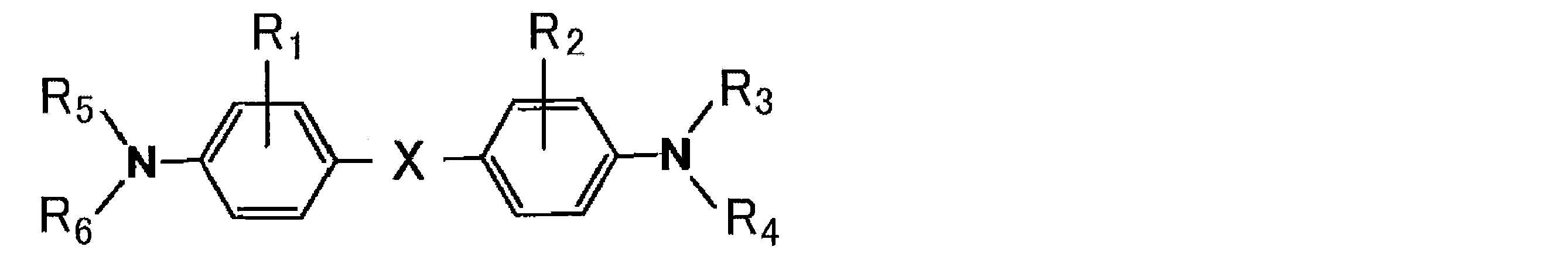
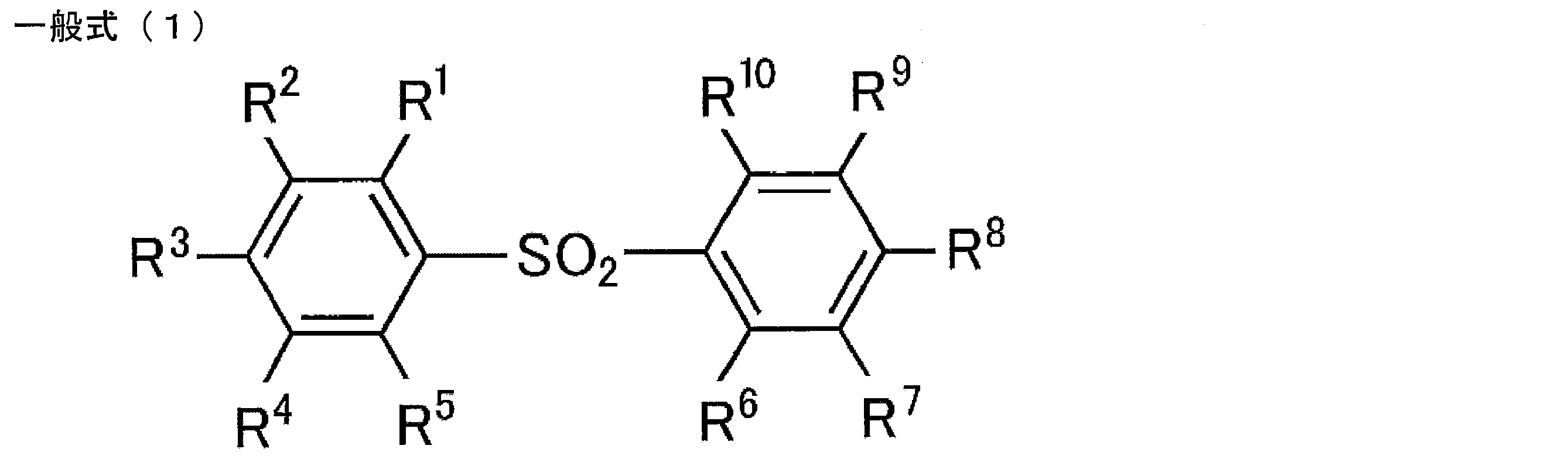
[2] 前記一般式(1)で表される化合物が、下記一般式(2)で表される構造を有することを特徴とする[1]に記載の発光材料。

[3] 前記一般式(1)で表される化合物が、下記一般式(3)で表される構造を有することを特徴とする[1]に記載の発光材料。

[4] 前記一般式(1)で表される化合物が、下記一般式(4)で表される構造を有することを特徴とする[1]に記載の発光材料。

[5] 前記一般式(1)で表される化合物が、下記一般式(5)で表される構造を有することを特徴とする[1]に記載の発光材料。

[7] 前記一般式(1)において、R1~R10が、各々独立に水素原子、置換もしくは無置換のアルキル基、または置換もしくは無置換のアルコキシ基、置換もしくは無置換のジアリールアミノ基、または置換もしくは無置換の9-カルバゾリル基を表し、R1~R10のうちの少なくとも1つが置換もしくは無置換のジアリールアミノ基、または置換もしくは無置換の9-カルバゾリル基であることを特徴とする[1]~[5]のいずれか一項に記載の発光材料。
[8] 前記一般式(1)において、R1~R10が、各々独立に水素原子、置換もしくは無置換のジアリールアミノ基、または置換もしくは無置換の9-カルバゾリル基を表し、R1~R10のうちの少なくとも1つが置換もしくは無置換のジアリールアミノ基、または置換もしくは無置換の9-カルバゾリル基であることを特徴とする[1]~[5]のいずれか一項に記載の発光材料。
[9] 前記一般式(1)において、R1~R10のうちの少なくとも1つが下記一般式(6)で表される構造を有することを特徴とする[1]~[8]のいずれか一項に記載の発光材料。

[10] 前記一般式(1)において、R1~R10のうちの少なくとも1つが下記一般式(7)で表される構造を有することを特徴とする[1]~[8]のいずれか一項に記載の発光材料。
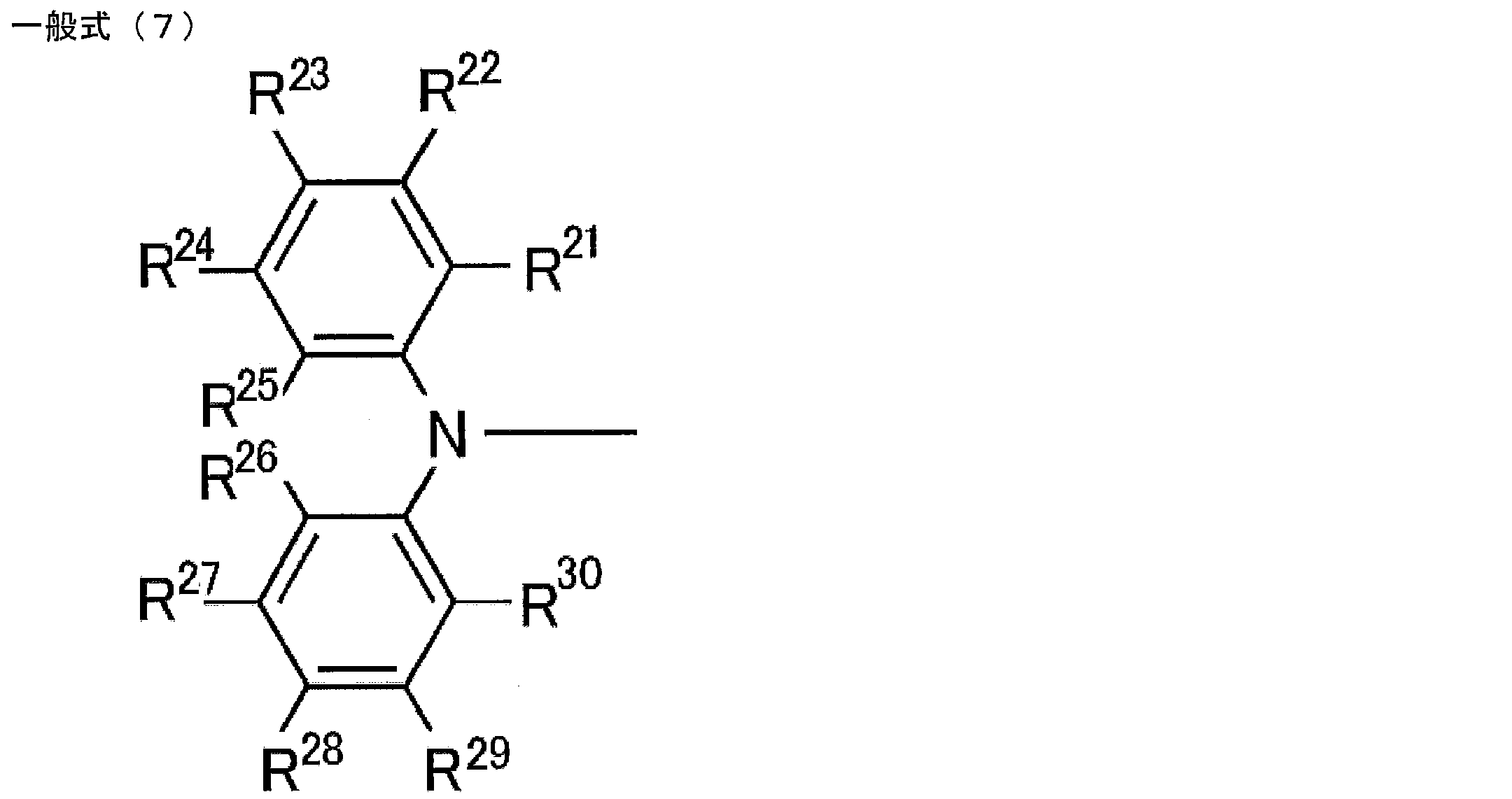
[11] 前記一般式(1)において、R1~R10のうちの少なくとも1つが下記一般式(8)で表される構造を有することを特徴とする[1]~[8]のいずれか一項に記載の発光材料。

[12] 前記一般式(1)において、R1~R10のうちの少なくとも1つが下記一般式(9)で表される構造を有することを特徴とする[1]~[8]のいずれか一項に記載の発光材料。

[13] [1]~[11]のいずれか1項に記載の発光材料からなる遅延蛍光体。
[14] [1]~[12]のいずれか1項に記載の発光材料を含む発光層を基板上に有することを特徴とする有機発光素子。
[15] 遅延蛍光を放射することを特徴とする[14]に記載の有機発光素子。
[16] 有機エレクトロルミネッセンス素子であることを特徴とする[14]または[15]に記載の有機発光素子。
[17] 下記一般式(1’)で表される化合物。
本発明の発光材料は、下記一般式(1)で表される化合物からなることを特徴とする。また、本発明の有機発光素子は、下記一般式(1)で表される化合物を発光層の発光材料として含むことを特徴とする。そこで、一般式(1)で表される化合物について、まず説明する。
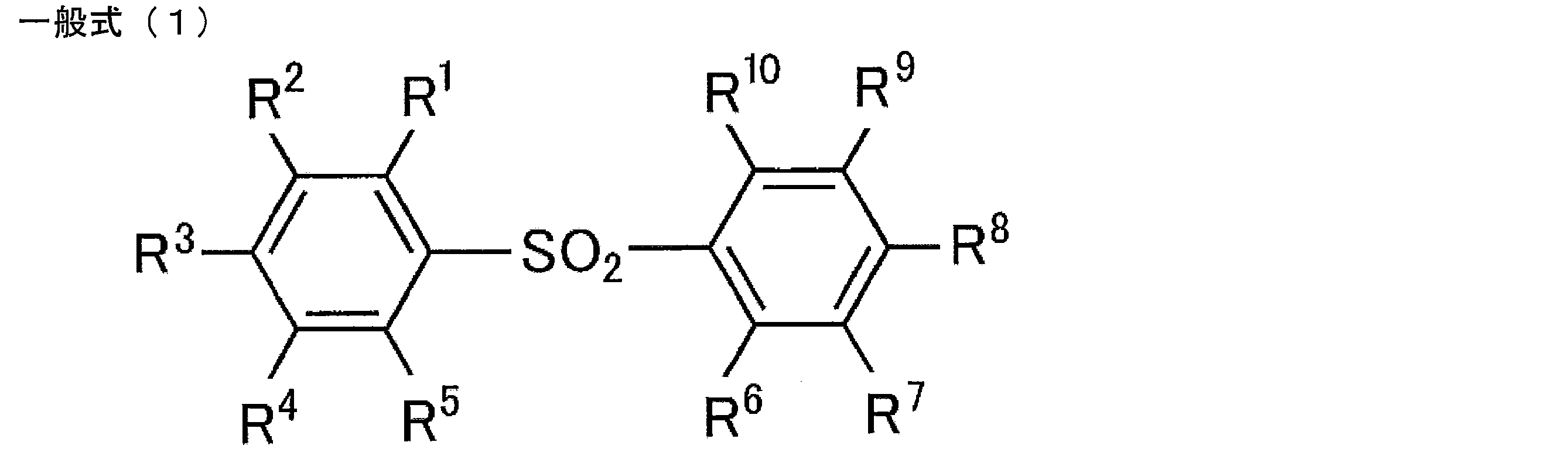

R11とR12、R12とR13、R13とR14、R14とR15、R16とR17、R17とR18、R18とR19、R19とR20は、それぞれ互いに結合して環状構造を形成してもよい。一般式(6)におけるR11~R20がとりうる置換基や環状構造の説明と好ましい範囲については、上記の一般式(1)における置換基や環状構造の説明と好ましい範囲を参照することができる。
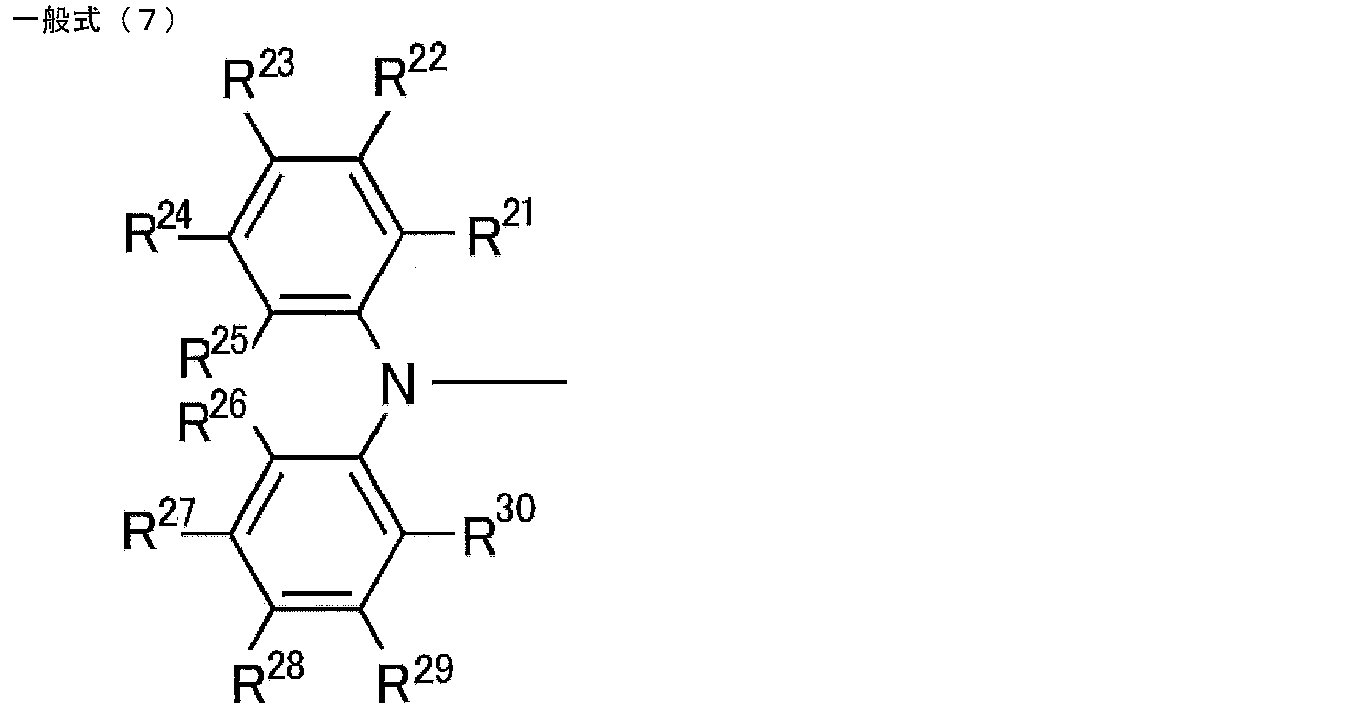

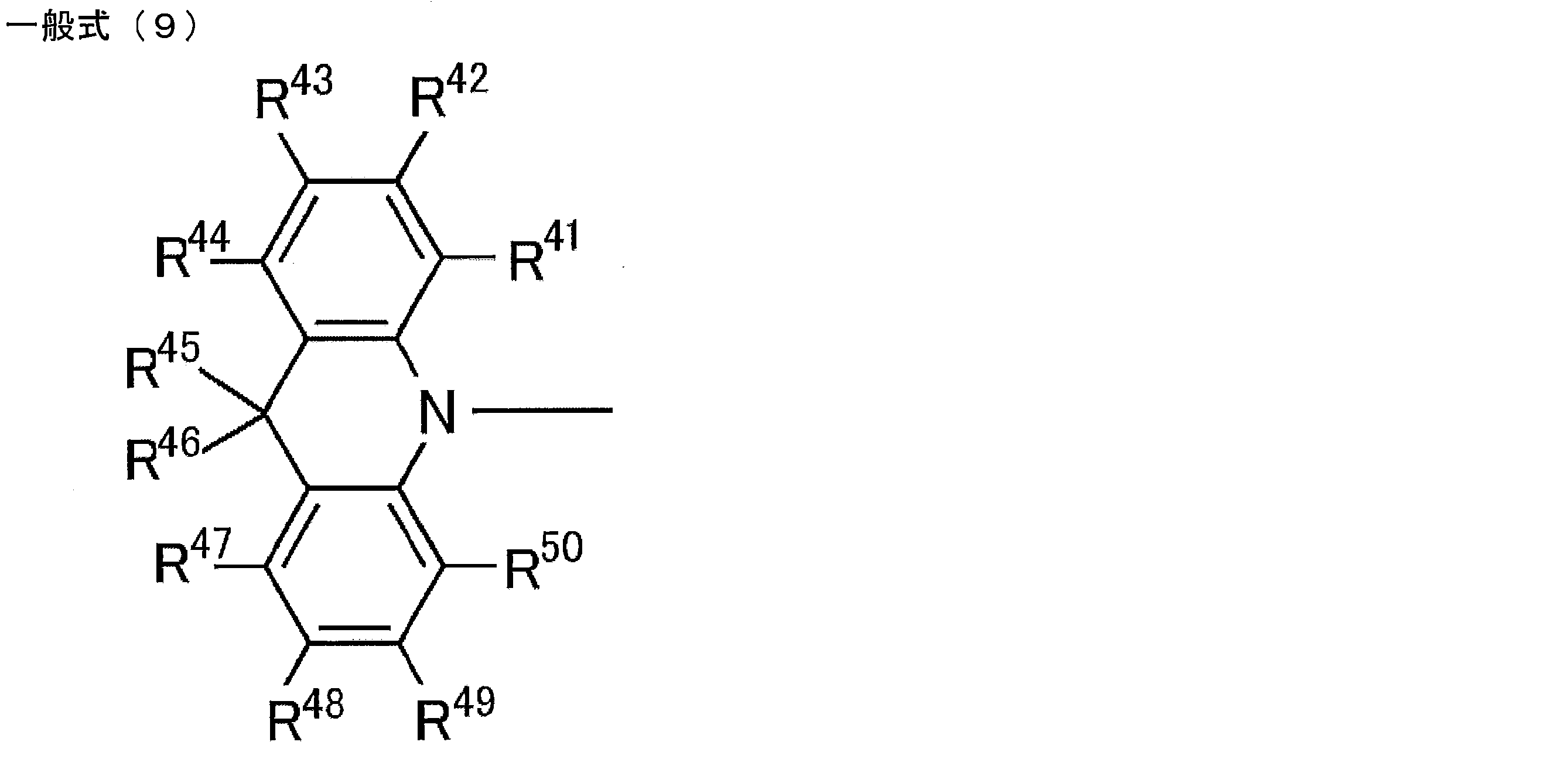
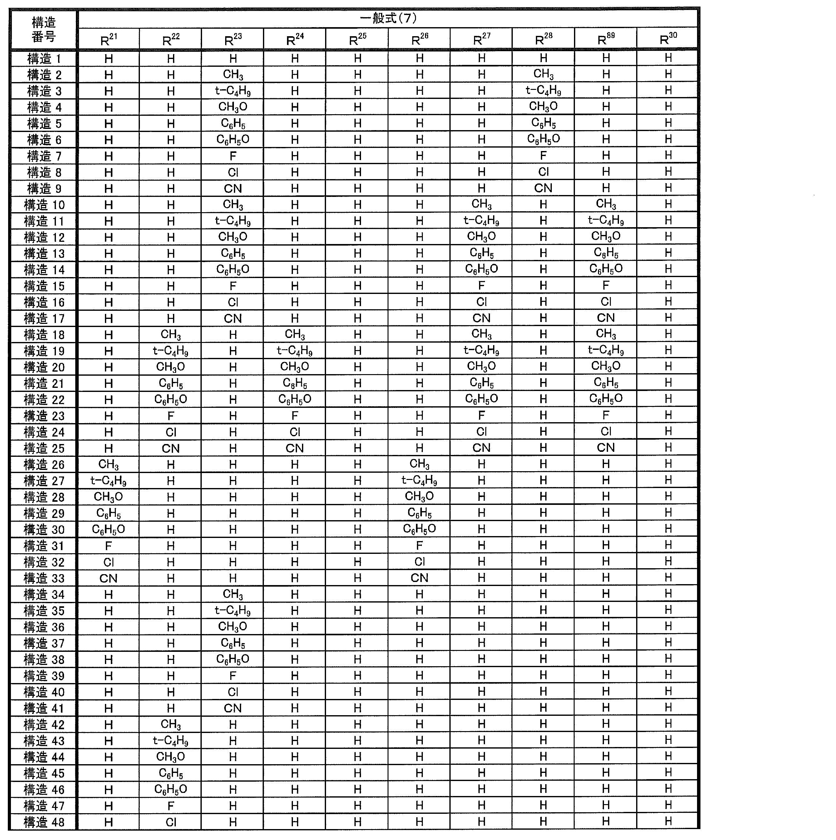
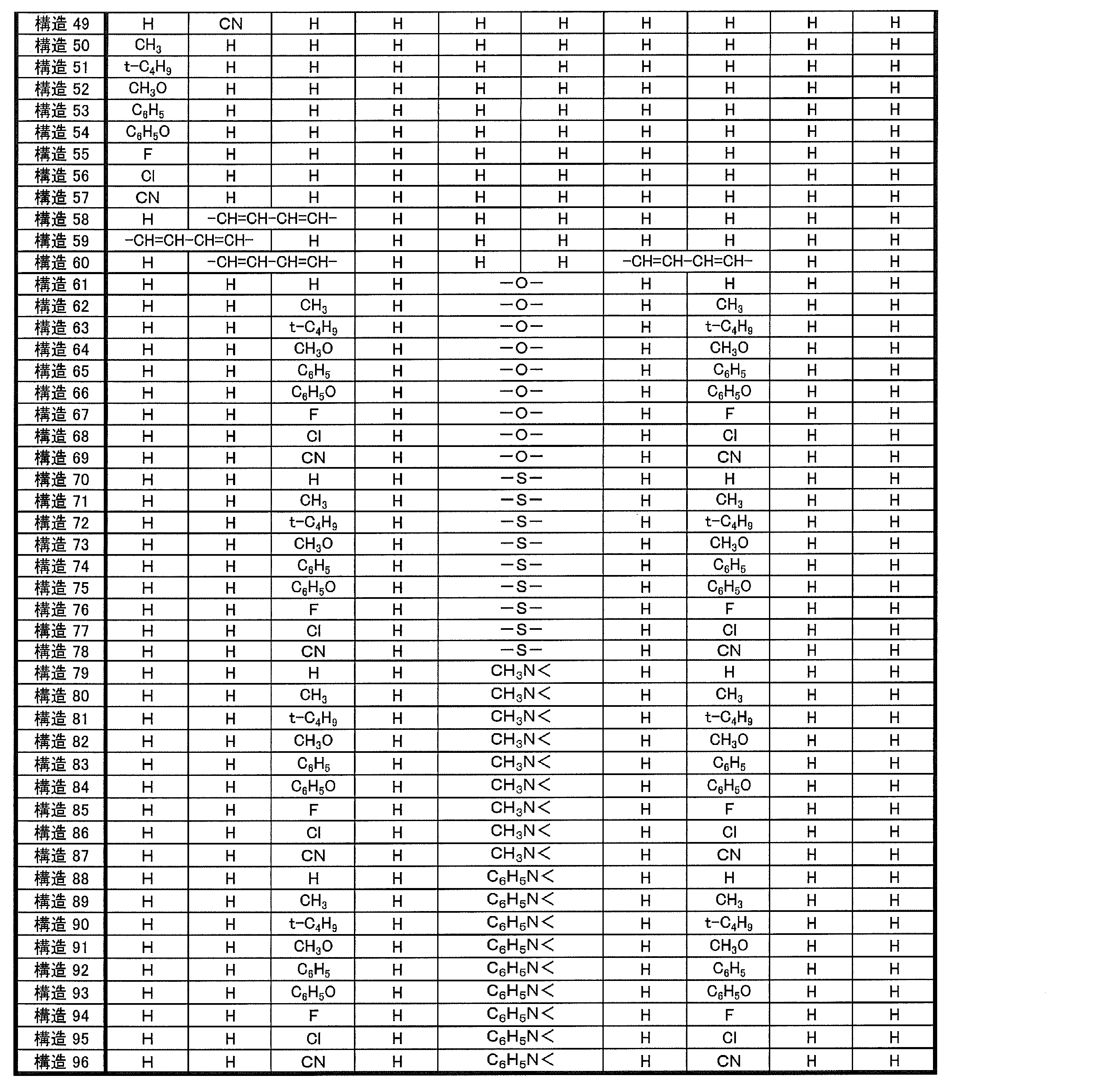

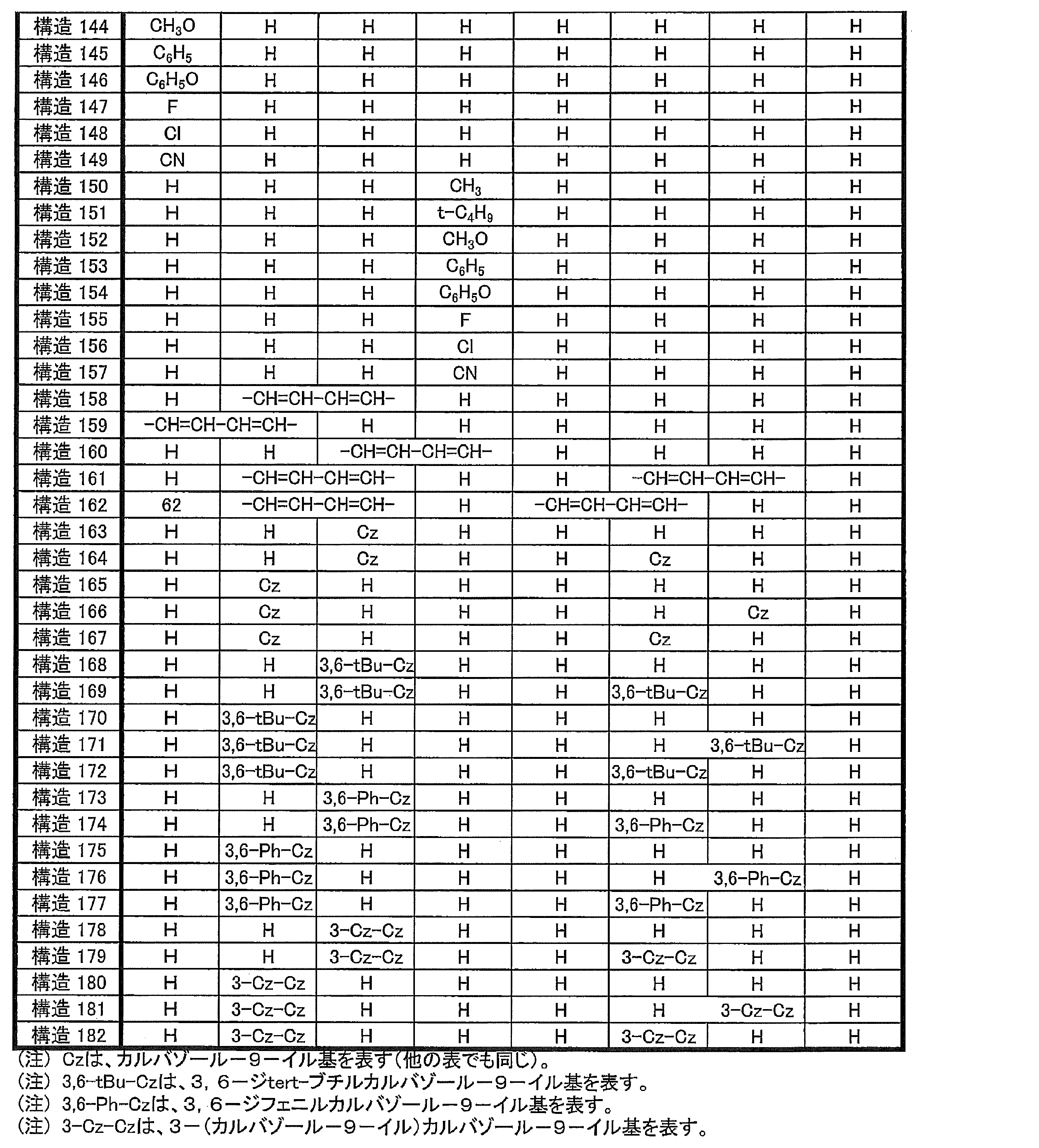
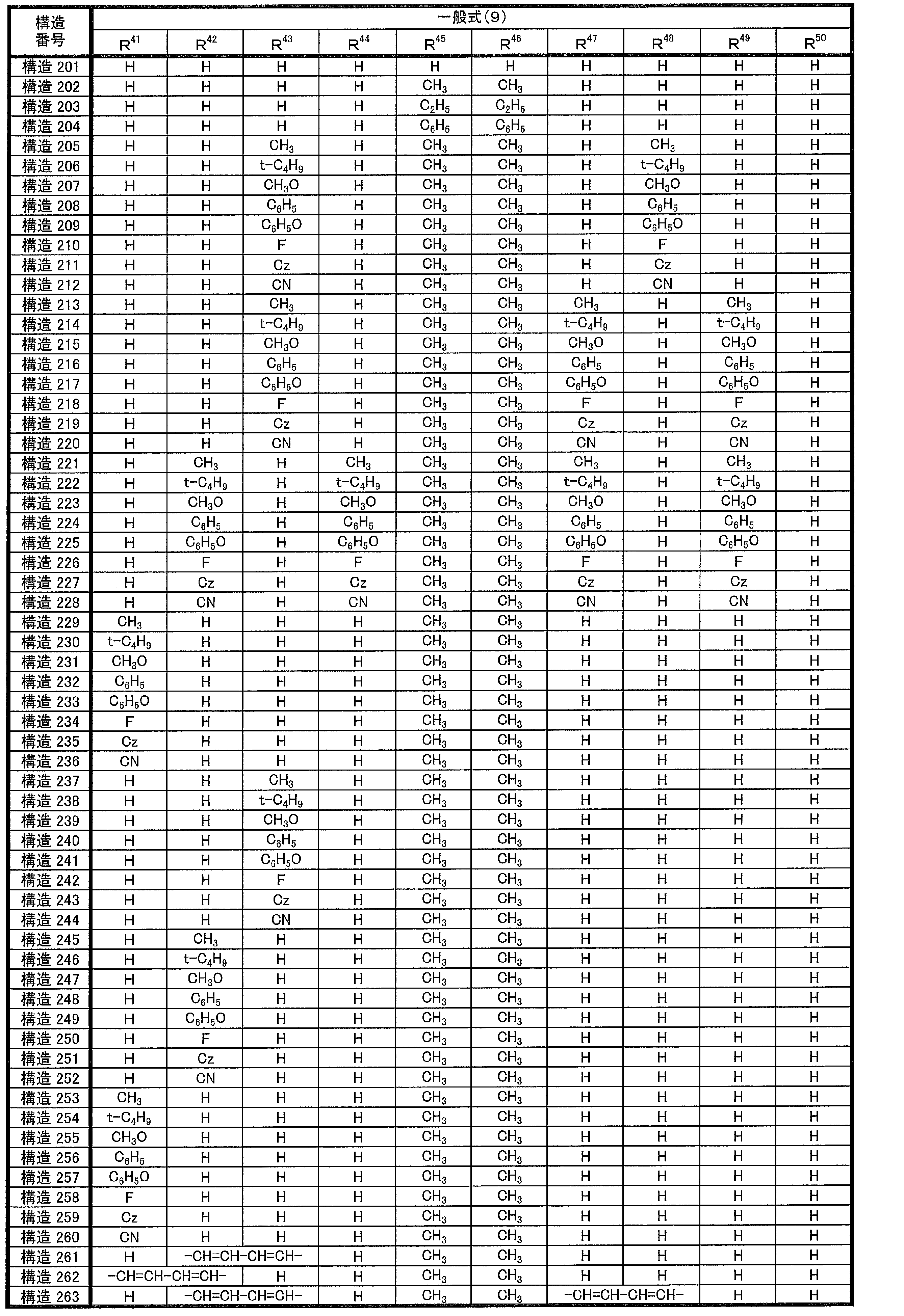
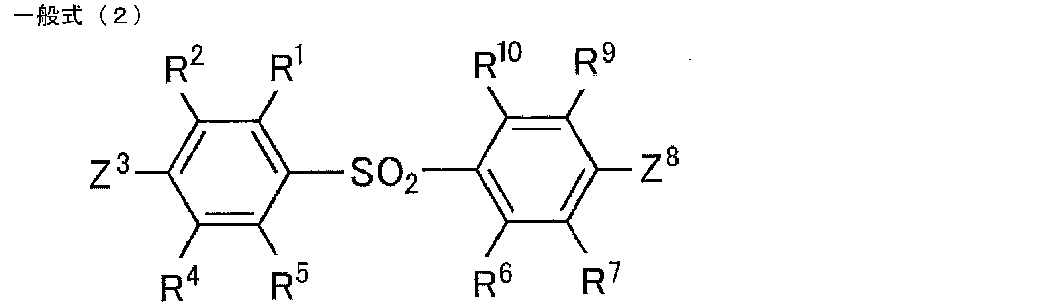
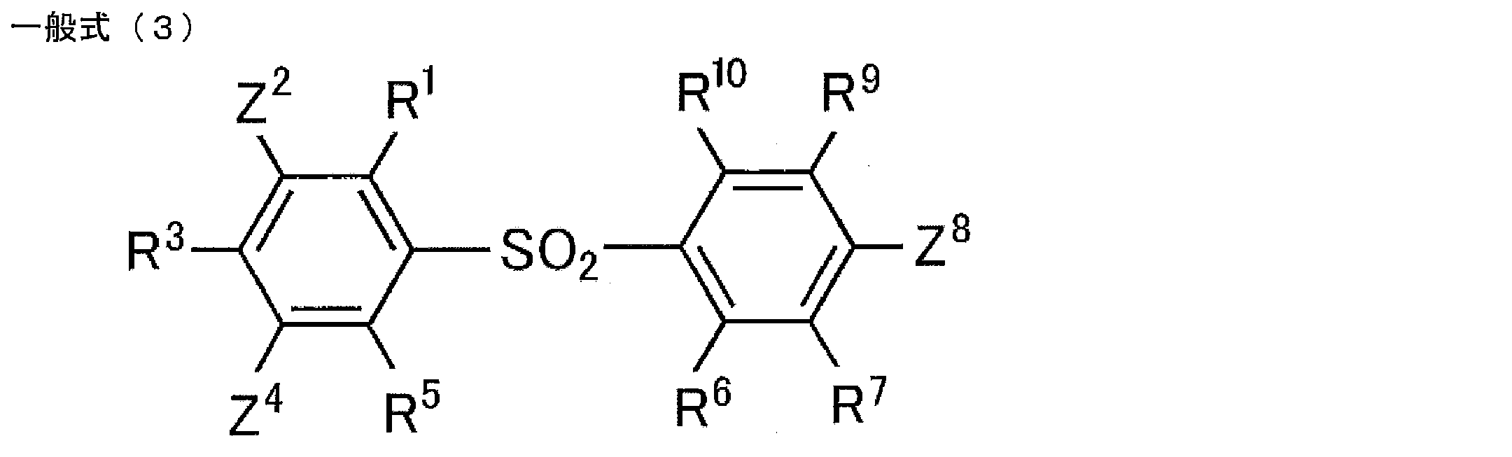


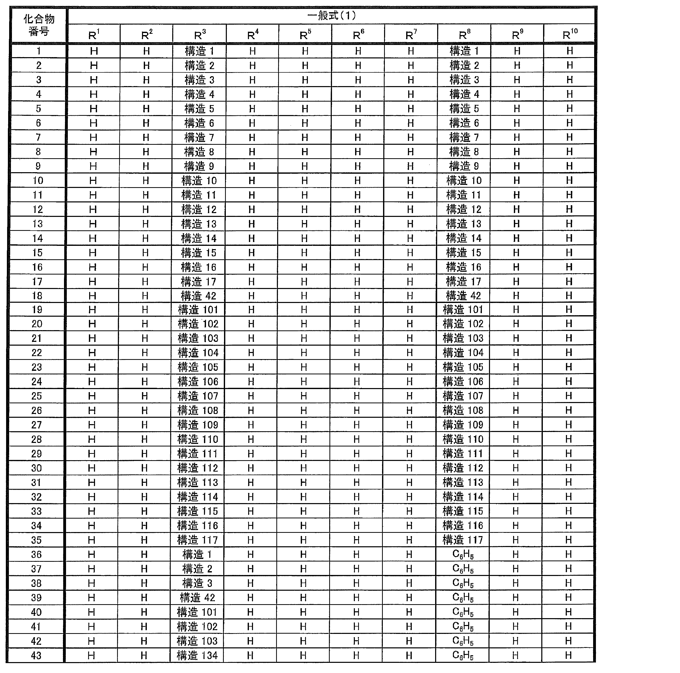


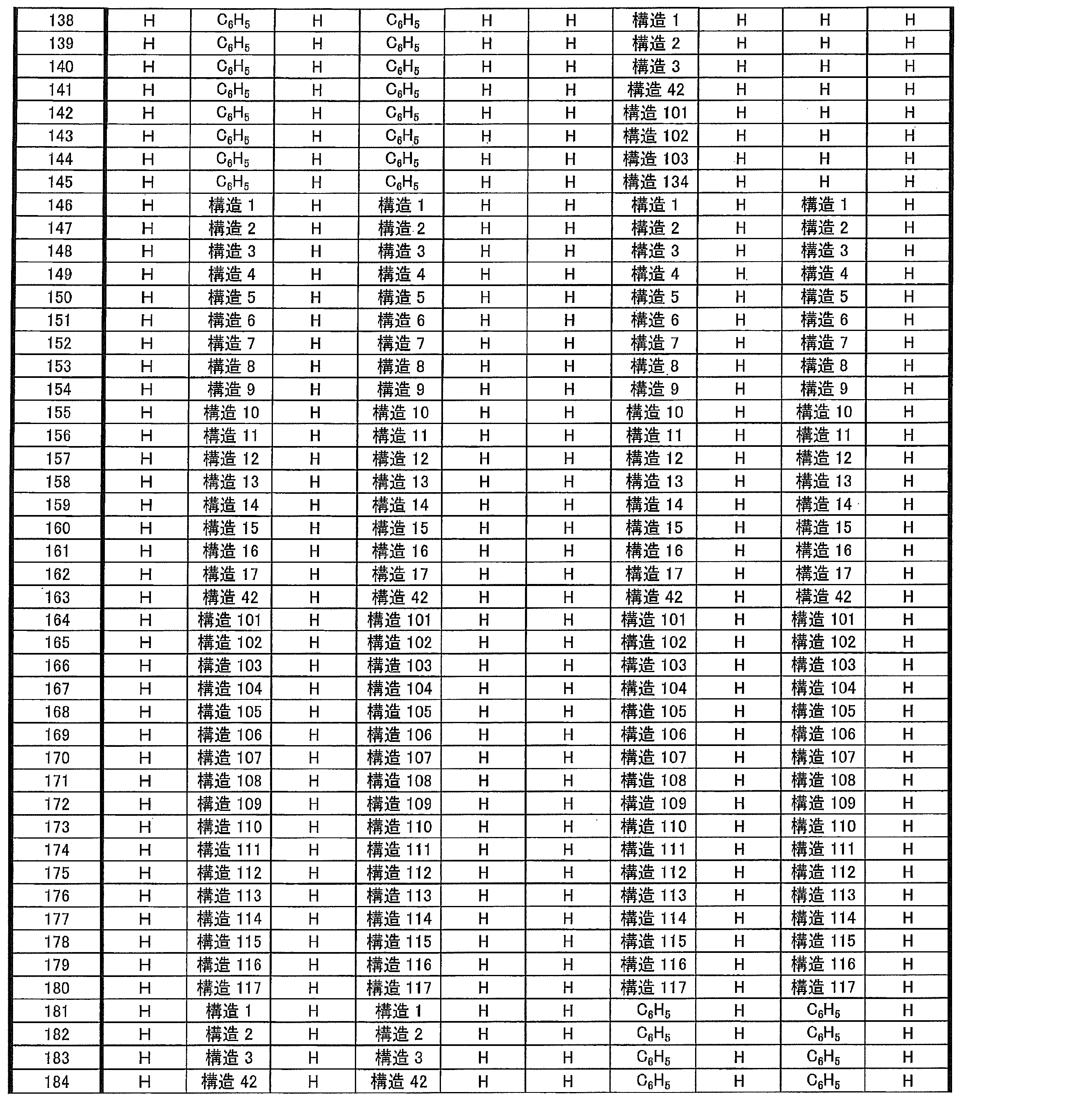


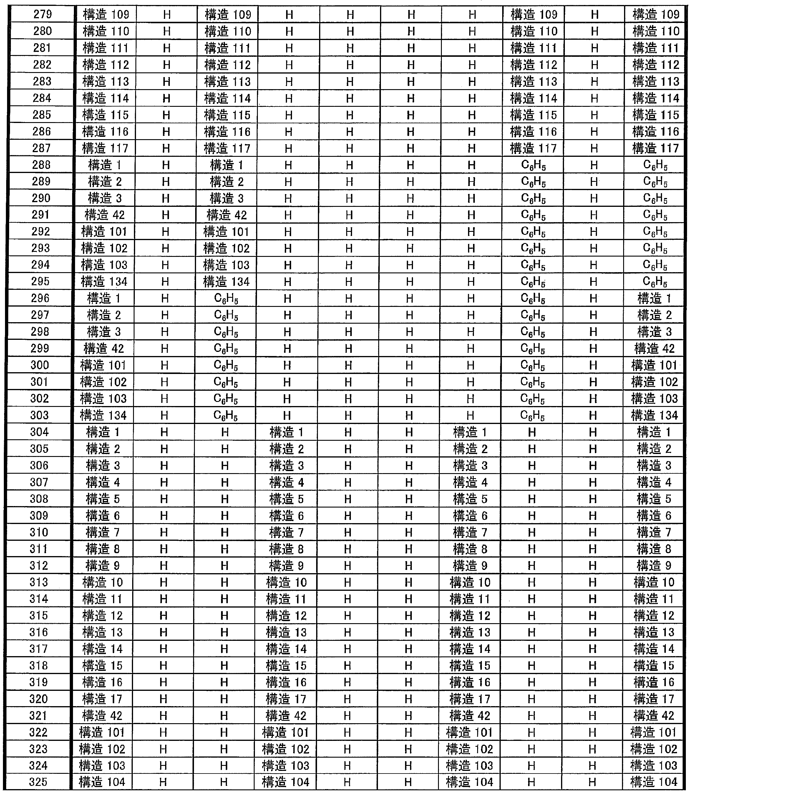
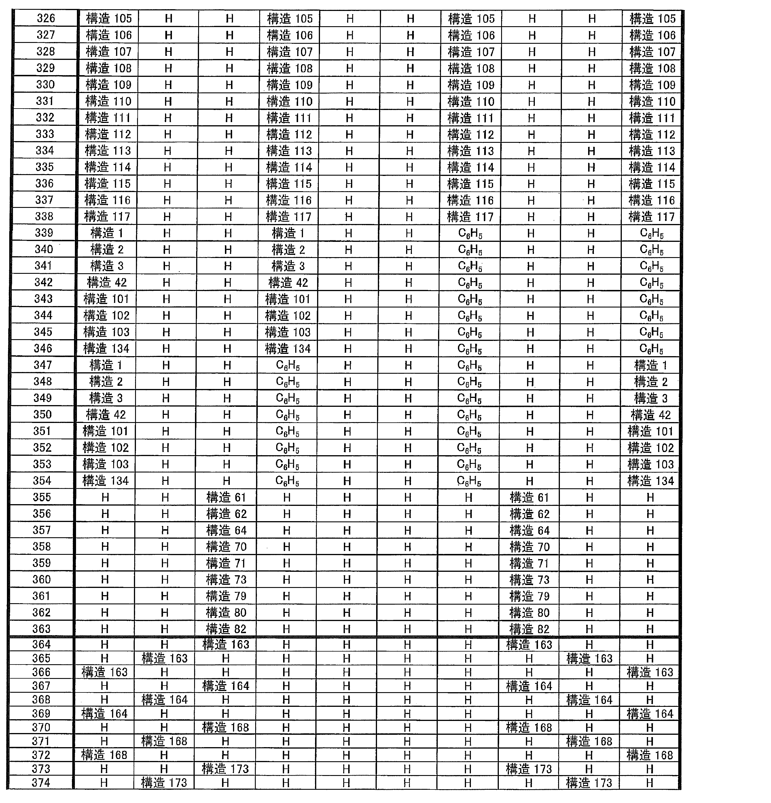
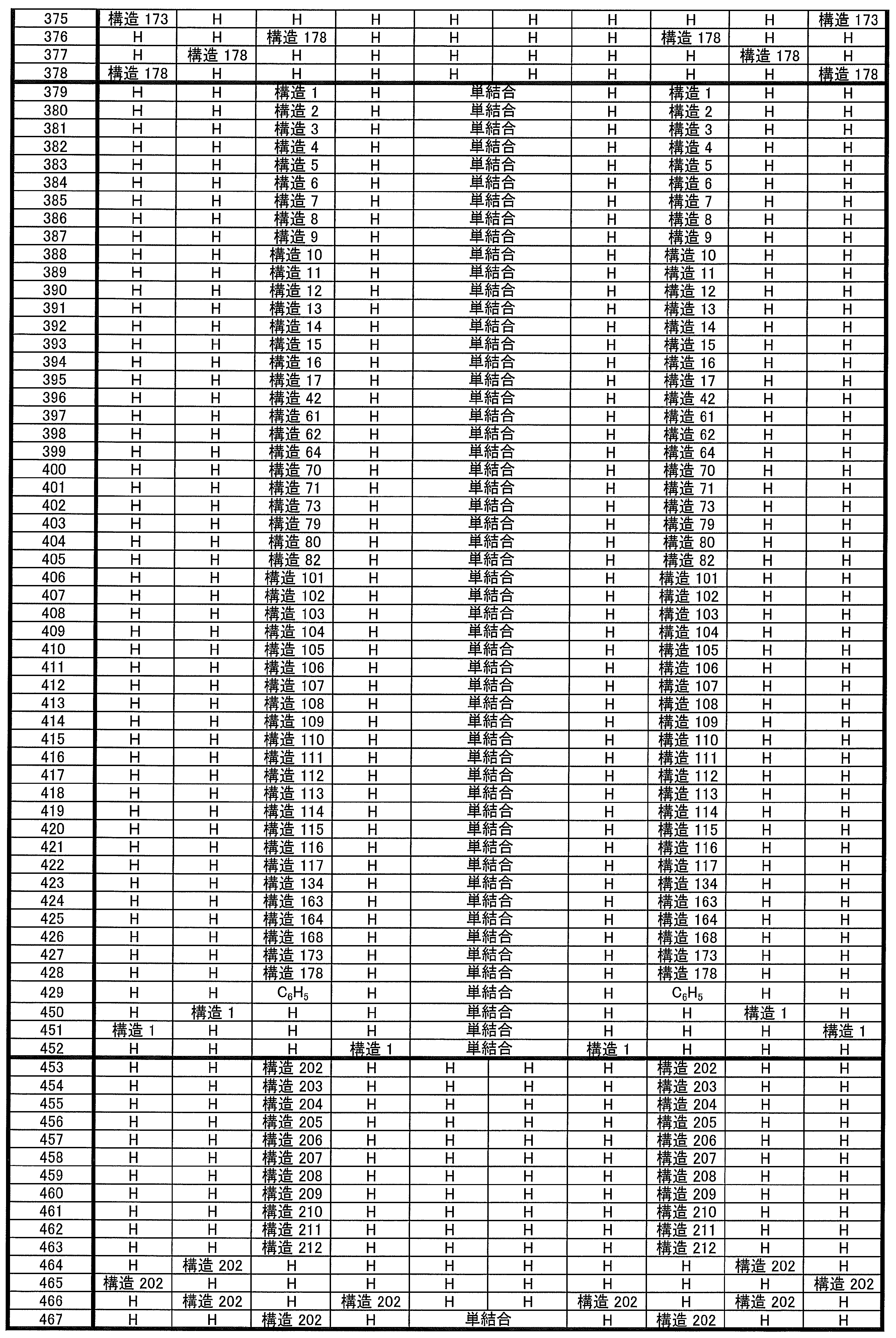
一般式(1)で表される化合物は、分子量にかかわらず塗布法で成膜してもよい。塗布法を用いれば、分子量が比較的大きな化合物であっても成膜することが可能である。
例えば、一般式(1)で表される構造を有する重合性モノマーを重合させた重合体を、有機発光素子の発光層に用いることが考えられる。具体的には、一般式(1)のR1~R10のいずれかに重合性官能基を有するモノマーを用意して、これを単独で重合させるか、他のモノマーとともに共重合させることにより、繰り返し単位を有する重合体を得て、その重合体を有機発光素子の発光層に用いることが考えられる。あるいは、一般式(1)で表される構造を有する化合物どうしをカップリングさせることにより、二量体や三量体を得て、それらを有機発光素子の発光層に用いることも考えられる。
一般式(10)および(11)において、R101、R102、R103およびR104は、各々独立に置換基を表す。好ましくは、炭素数1~6の置換もしくは無置換のアルキル基、炭素数1~6の置換もしくは無置換のアルコキシ基、ハロゲン原子であり、より好ましくは炭素数1~3の無置換のアルキル基、炭素数1~3の無置換のアルコキシ基、フッ素原子、塩素原子であり、さらに好ましくは炭素数1~3の無置換のアルキル基、炭素数1~3の無置換のアルコキシ基である。

一般式(1)で表される化合物は、熱活性化遅延蛍光材料であることが好ましい。遅延蛍光材料として有機エレクトロルミネッセンス素子の発光層に用いれば、高い発光効率を従来よりも安価に達成しうる。従来は、発光効率が高い有機エレクトロルミネッセンス素子を製造するために、励起子生成効率が高いリン光材料を用いた研究が活発に行われてきた。しかしながら、リン光材料を用いる場合は、IrやPtといった希少金属を利用する必要があるため、コストが高くなるという問題があった。遅延蛍光材料を用いれば、このような高価な材料を必要としないため、発光効率が高い有機エレクトロルミネッセンス素子を安価に提供することが可能になる。
本発明の一般式(1)で表される化合物は、有機発光素子の発光材料として有用である。このため、本発明の一般式(1)で表される化合物は、有機発光素子の発光層に発光材料として効果的に用いることができる。一般式(1)で表される化合物の中には、遅延蛍光を放射する遅延蛍光材料(遅延蛍光体)が含まれている。すなわち本発明は、一般式(1)で表される構造を有する遅延蛍光体の発明と、一般式(1)で表される化合物を遅延蛍光体として使用する発明と、一般式(1)で表される化合物を用いて遅延蛍光を発光させる方法の発明も提供する。そのような化合物を発光材料として用いた有機発光素子は、遅延蛍光を放射し、発光効率が高いという特徴を有する。その原理を、有機エレクトロルミネッセンス素子を例にとって説明すると以下のようになる。
以下において、有機エレクトロルミネッセンス素子の各部材および各層について説明する。なお、基板と発光層の説明は有機フォトルミネッセンス素子の基板と発光層にも該当する。
本発明の有機エレクトロルミネッセンス素子は、基板に支持されていることが好ましい。この基板については、特に制限はなく、従来から有機エレクトロルミネッセンス素子に慣用されているものであればよく、例えば、ガラス、透明プラスチック、石英、シリコンなどからなるものを用いることができる。
有機エレクトロルミネッセンス素子における陽極としては、仕事関数の大きい(4eV以上)金属、合金、電気伝導性化合物およびこれらの混合物を電極材料とするものが好ましく用いられる。このような電極材料の具体例としてはAu等の金属、CuI、インジウムチンオキシド(ITO)、SnO2、ZnO等の導電性透明材料が挙げられる。また、IDIXO(In2O3-ZnO)等非晶質で透明導電膜を作製可能な材料を用いてもよい。陽極はこれらの電極材料を蒸着やスパッタリング等の方法により、薄膜を形成させ、フォトリソグラフィー法で所望の形状のパターンを形成してもよく、あるいはパターン精度をあまり必要としない場合は(100μm以上程度)、上記電極材料の蒸着やスパッタリング時に所望の形状のマスクを介してパターンを形成してもよい。あるいは、有機導電性化合物のように塗布可能な材料を用いる場合には、印刷方式、コーティング方式等湿式成膜法を用いることもできる。この陽極より発光を取り出す場合には、透過率を10%より大きくすることが望ましく、また陽極としてのシート抵抗は数百Ω/□以下が好ましい。さらに膜厚は材料にもよるが、通常10~1000nm、好ましくは10~200nmの範囲で選ばれる。
一方、陰極としては、仕事関数の小さい(4eV以下)金属(電子注入性金属と称する)、合金、電気伝導性化合物およびこれらの混合物を電極材料とするものが用いられる。このような電極材料の具体例としては、ナトリウム、ナトリウム-カリウム合金、マグネシウム、リチウム、マグネシウム/銅混合物、マグネシウム/銀混合物、マグネシウム/アルミニウム混合物、マグネシウム/インジウム混合物、アルミニウム/酸化アルミニウム(Al2O3)混合物、インジウム、リチウム/アルミニウム混合物、希土類金属等が挙げられる。これらの中で、電子注入性および酸化等に対する耐久性の点から、電子注入性金属とこれより仕事関数の値が大きく安定な金属である第二金属との混合物、例えば、マグネシウム/銀混合物、マグネシウム/アルミニウム混合物、マグネシウム/インジウム混合物、アルミニウム/酸化アルミニウム(Al2O3)混合物、リチウム/アルミニウム混合物、アルミニウム等が好適である。陰極はこれらの電極材料を蒸着やスパッタリング等の方法により薄膜を形成させることにより、作製することができる。また、陰極としてのシート抵抗は数百Ω/□以下が好ましく、膜厚は通常10nm~5μm、好ましくは50~200nmの範囲で選ばれる。なお、発光した光を透過させるため、有機エレクトロルミネッセンス素子の陽極または陰極のいずれか一方が、透明または半透明であれば発光輝度が向上し好都合である。
また、陽極の説明で挙げた導電性透明材料を陰極に用いることで、透明または半透明の陰極を作製することができ、これを応用することで陽極と陰極の両方が透過性を有する素子を作製することができる。
発光層は、陽極および陰極のそれぞれから注入された正孔および電子が再結合することにより励起子が生成した後、発光する層であり、発光材料を単独で発光層に使用しても良いが、好ましくは発光材料とホスト材料を含む。発光材料としては、一般式(1)で表される本発明の化合物群から選ばれる1種または2種以上を用いることができる。本発明の有機エレクトロルミネッセンス素子および有機フォトルミネッセンス素子が高い発光効率を発現するためには、発光材料に生成した一重項励起子および三重項励起子を、発光材料中に閉じ込めることが重要である。従って、発光層中に発光材料に加えてホスト材料を用いることが好ましい。ホスト材料としては、励起一重項エネルギー、励起三重項エネルギーの少なくとも何れか一方が本発明の発光材料よりも高い値を有する有機化合物を用いることができる。その結果、本発明の発光材料に生成した一重項励起子および三重項励起子を、本発明の発光材料の分子中に閉じ込めることが可能となり、その発光効率を十分に引き出すことが可能となる。もっとも、一重項励起子および三重項励起子を十分に閉じ込めることができなくても、高い発光効率を得ることが可能な場合もあるため、高い発光効率を実現しうるホスト材料であれば特に制約なく本発明に用いることができる。本発明の有機発光素子または有機エレクトロルミネッセンス素子において、発光は発光層に含まれる本発明の発光材料から生じる。この発光は蛍光発光および遅延蛍光発光の両方を含む。但し、発光の一部或いは部分的にホスト材料からの発光があってもかまわない。
ホスト材料を用いる場合、発光材料である本発明の化合物が発光層中に含有される量は0.1重量%以上であることが好ましく、1重量%以上であることがより好ましく、また、50重量%以下であることが好ましく、20重量%以下であることがより好ましく、10重量%以下であることがさらに好ましい。
発光層におけるホスト材料としては、正孔輸送能、電子輸送能を有し、かつ発光の長波長化を防ぎ、なおかつ高いガラス転移温度を有する有機化合物であることが好ましい。
注入層とは、駆動電圧低下や発光輝度向上のために電極と有機層間に設けられる層のことで、正孔注入層と電子注入層があり、陽極と発光層または正孔輸送層の間、および陰極と発光層または電子輸送層との間に存在させてもよい。注入層は必要に応じて設けることができる。
阻止層は、発光層中に存在する電荷(電子もしくは正孔)および/または励起子の発光層外への拡散を阻止することができる層である。電子阻止層は、発光層および正孔輸送層の間に配置されることができ、電子が正孔輸送層の方に向かって発光層を通過することを阻止する。同様に、正孔阻止層は発光層および電子輸送層の間に配置されることができ、正孔が電子輸送層の方に向かって発光層を通過することを阻止する。阻止層はまた、励起子が発光層の外側に拡散することを阻止するために用いることができる。すなわち電子阻止層、正孔阻止層はそれぞれ励起子阻止層としての機能も兼ね備えることができる。本明細書でいう電子阻止層または励起子阻止層は、一つの層で電子阻止層および励起子阻止層の機能を有する層を含む意味で使用される。
正孔阻止層とは広い意味では電子輸送層の機能を有する。正孔阻止層は電子を輸送しつつ、正孔が電子輸送層へ到達することを阻止する役割があり、これにより発光層中での電子と正孔の再結合確率を向上させることができる。正孔阻止層の材料としては、後述する電子輸送層の材料を必要に応じて用いることができる。
電子阻止層とは、広い意味では正孔を輸送する機能を有する。電子阻止層は正孔を輸送しつつ、電子が正孔輸送層へ到達することを阻止する役割があり、これにより発光層中での電子と正孔が再結合する確率を向上させることができる。
励起子阻止層とは、発光層内で正孔と電子が再結合することにより生じた励起子が電荷輸送層に拡散することを阻止するための層であり、本層の挿入により励起子を効率的に発光層内に閉じ込めることが可能となり、素子の発光効率を向上させることができる。励起子阻止層は発光層に隣接して陽極側、陰極側のいずれにも挿入することができ、両方同時に挿入することも可能である。すなわち、励起子阻止層を陽極側に有する場合、正孔輸送層と発光層の間に、発光層に隣接して該層を挿入することができ、陰極側に挿入する場合、発光層と陰極との間に、発光層に隣接して該層を挿入することができる。また、陽極と、発光層の陽極側に隣接する励起子阻止層との間には、正孔注入層や電子阻止層などを有することができ、陰極と、発光層の陰極側に隣接する励起子阻止層との間には、電子注入層、電子輸送層、正孔阻止層などを有することができる。阻止層を配置する場合、阻止層として用いる材料の励起一重項エネルギーおよび励起三重項エネルギーの少なくともいずれか一方は、発光材料の励起一重項エネルギーおよび励起三重項エネルギーよりも高いことが好ましい。
正孔輸送層とは正孔を輸送する機能を有する正孔輸送材料からなり、正孔輸送層は単層または複数層設けることができる。
正孔輸送材料としては、正孔の注入または輸送、電子の障壁性のいずれかを有するものであり、有機物、無機物のいずれであってもよい。使用できる公知の正孔輸送材料としては例えば、トリアゾール誘導体、オキサジアゾール誘導体、イミダゾール誘導体、カルバゾール誘導体、インドロカルバゾール誘導体、ポリアリールアルカン誘導体、ピラゾリン誘導体およびピラゾロン誘導体、フェニレンジアミン誘導体、アリールアミン誘導体、アミノ置換カルコン誘導体、オキサゾール誘導体、スチリルアントラセン誘導体、フルオレノン誘導体、ヒドラゾン誘導体、スチルベン誘導体、シラザン誘導体、アニリン系共重合体、また導電性高分子オリゴマー、特にチオフェンオリゴマー等が挙げられるが、ポルフィリン化合物、芳香族第3級アミン化合物およびスチリルアミン化合物を用いることが好ましく、芳香族第3級アミン化合物を用いることがより好ましい。
電子輸送層とは電子を輸送する機能を有する材料からなり、電子輸送層は単層または複数層設けることができる。
電子輸送材料(正孔阻止材料を兼ねる場合もある)としては、陰極より注入された電子を発光層に伝達する機能を有していればよい。使用できる電子輸送層としては例えば、ニトロ置換フルオレン誘導体、ジフェニルキノン誘導体、チオピランジオキシド誘導体、カルボジイミド、フレオレニリデンメタン誘導体、アントラキノジメタンおよびアントロン誘導体、オキサジアゾール誘導体等が挙げられる。さらに、上記オキサジアゾール誘導体において、オキサジアゾール環の酸素原子を硫黄原子に置換したチアジアゾール誘導体、電子吸引基として知られているキノキサリン環を有するキノキサリン誘導体も、電子輸送材料として用いることができる。さらにこれらの材料を高分子鎖に導入した、またはこれらの材料を高分子の主鎖とした高分子材料を用いることもできる。
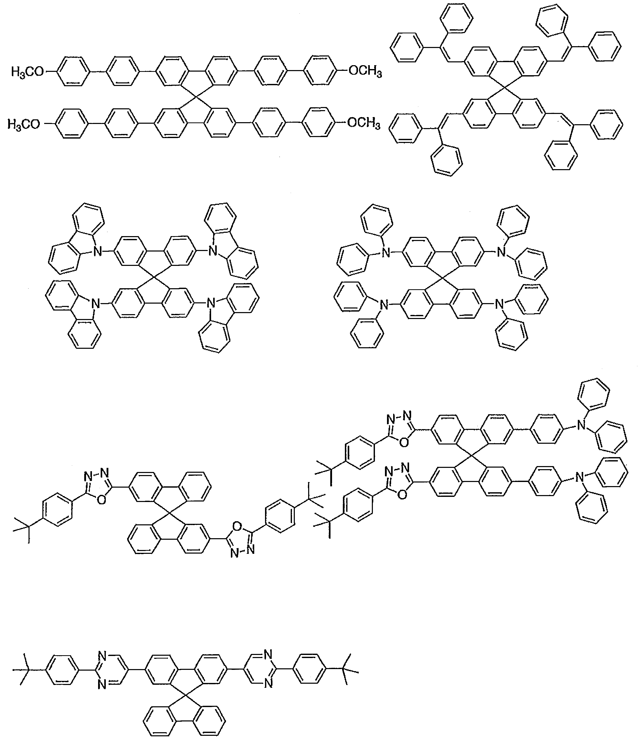
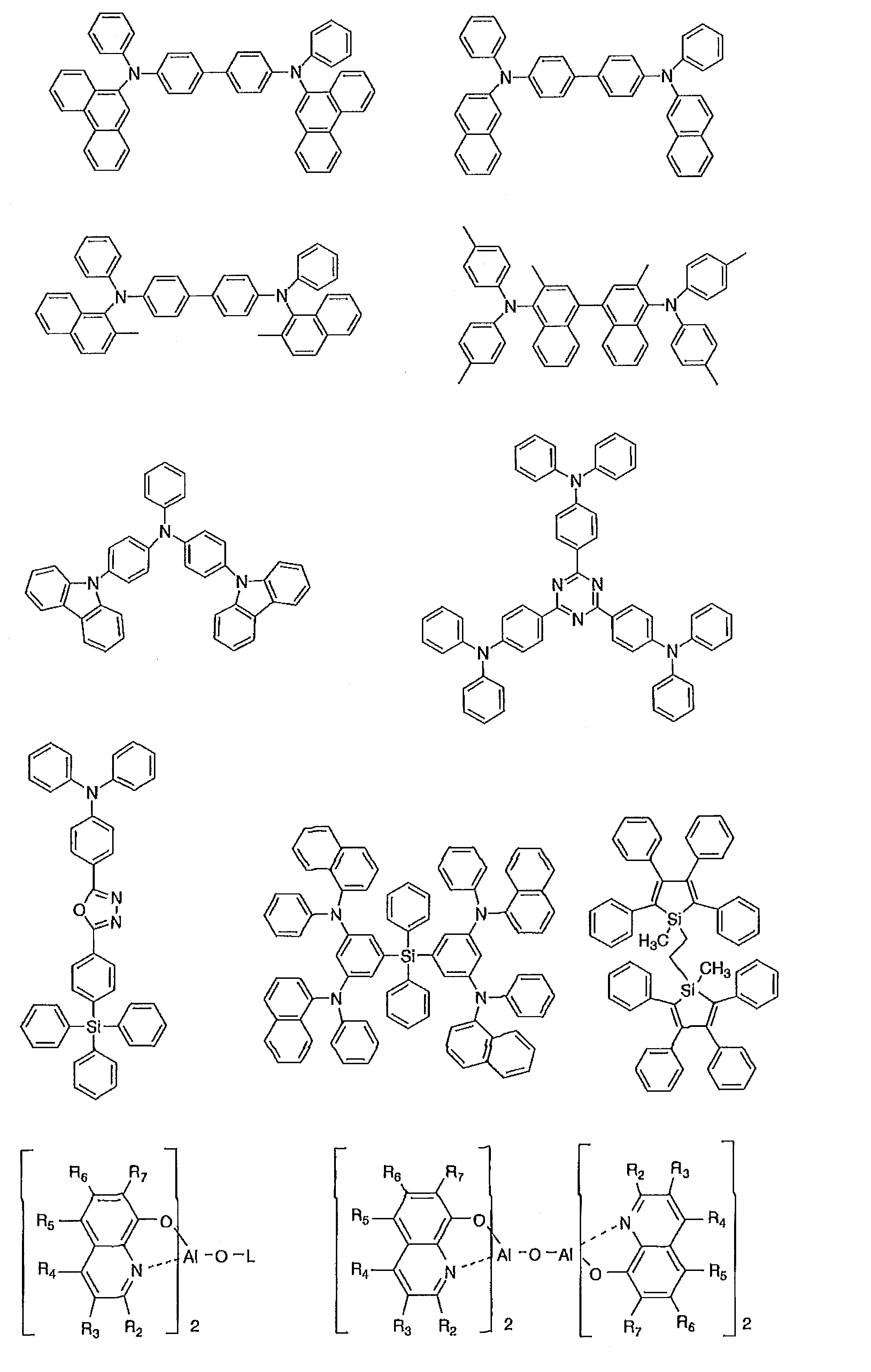

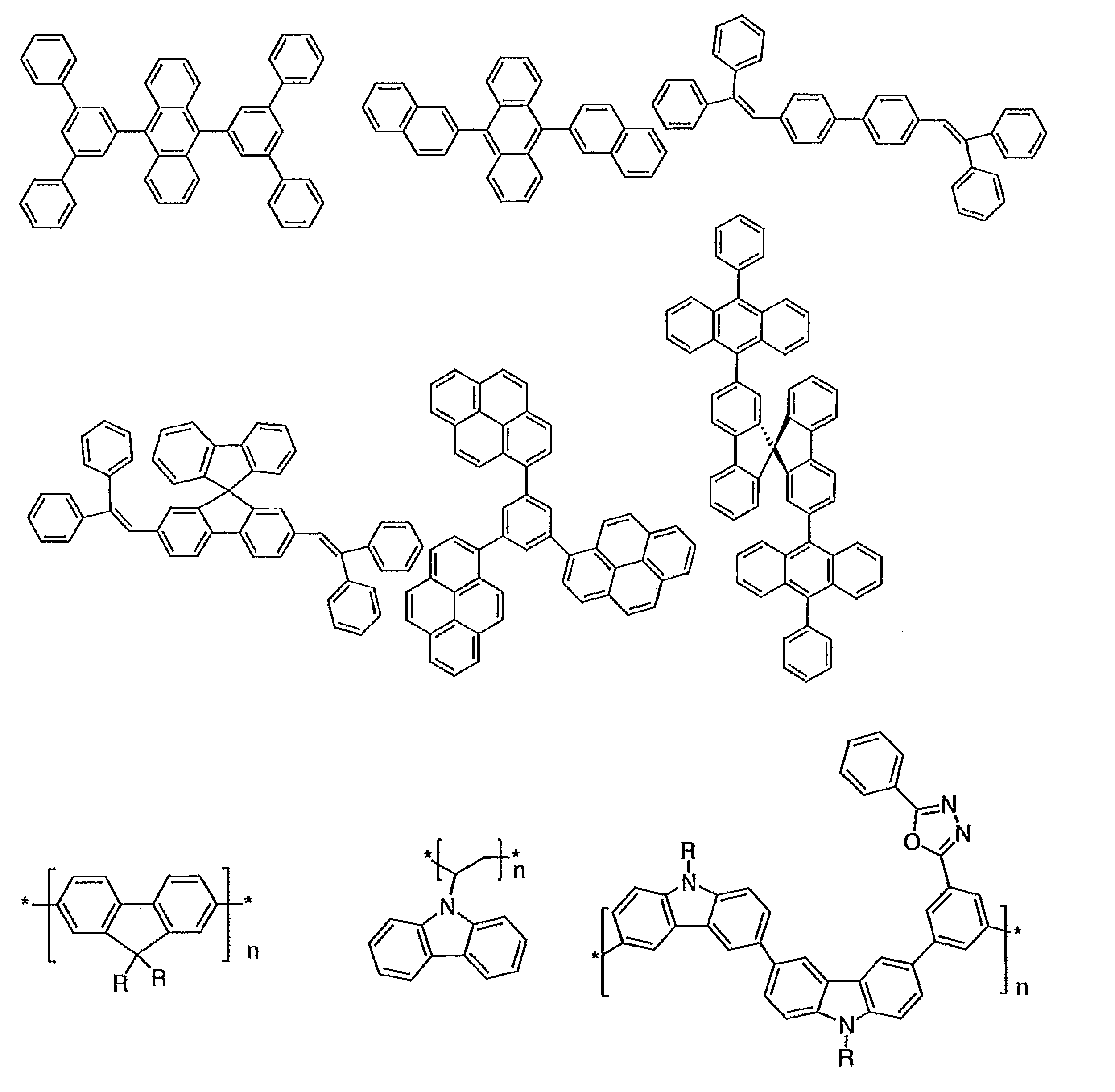


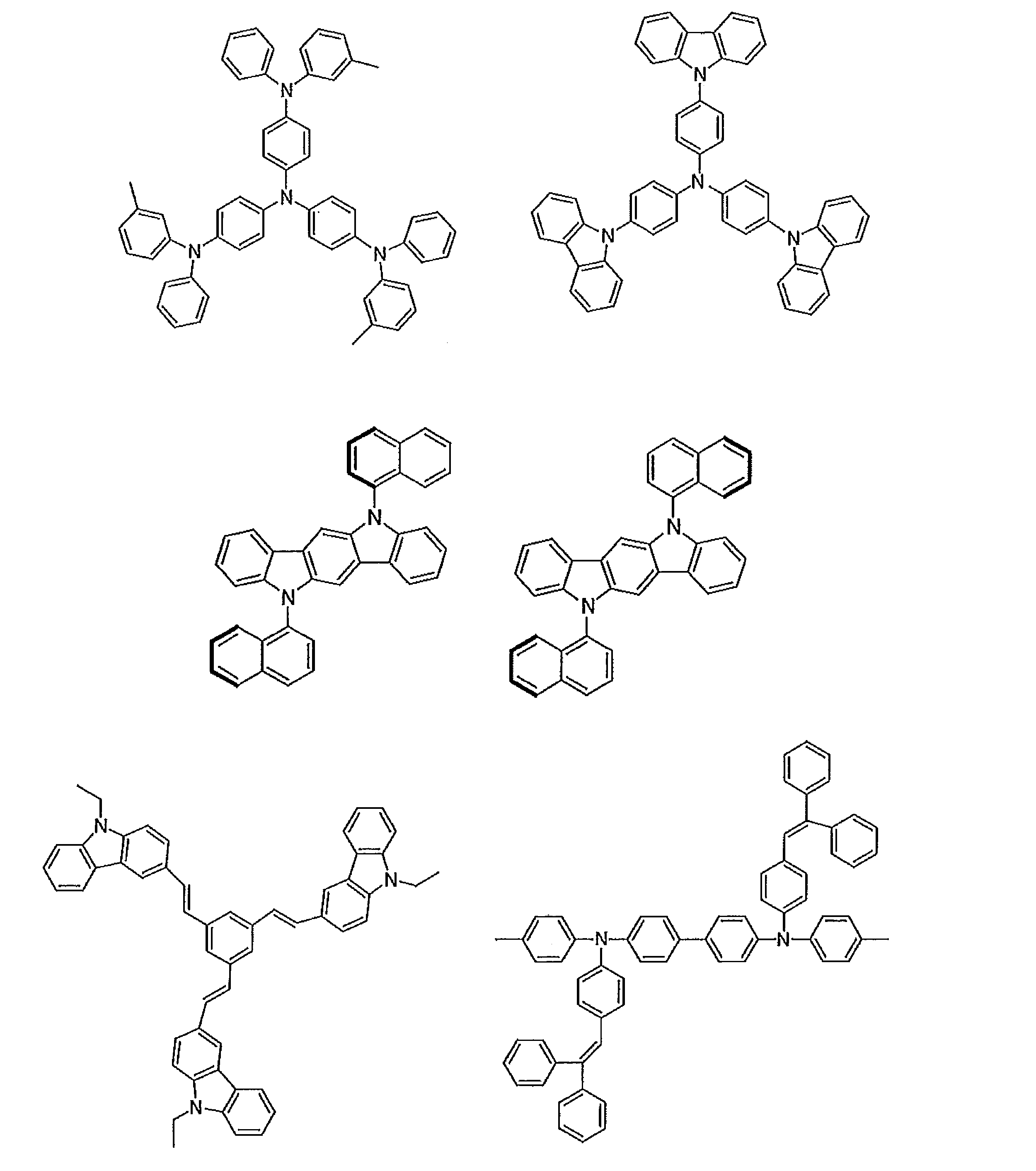


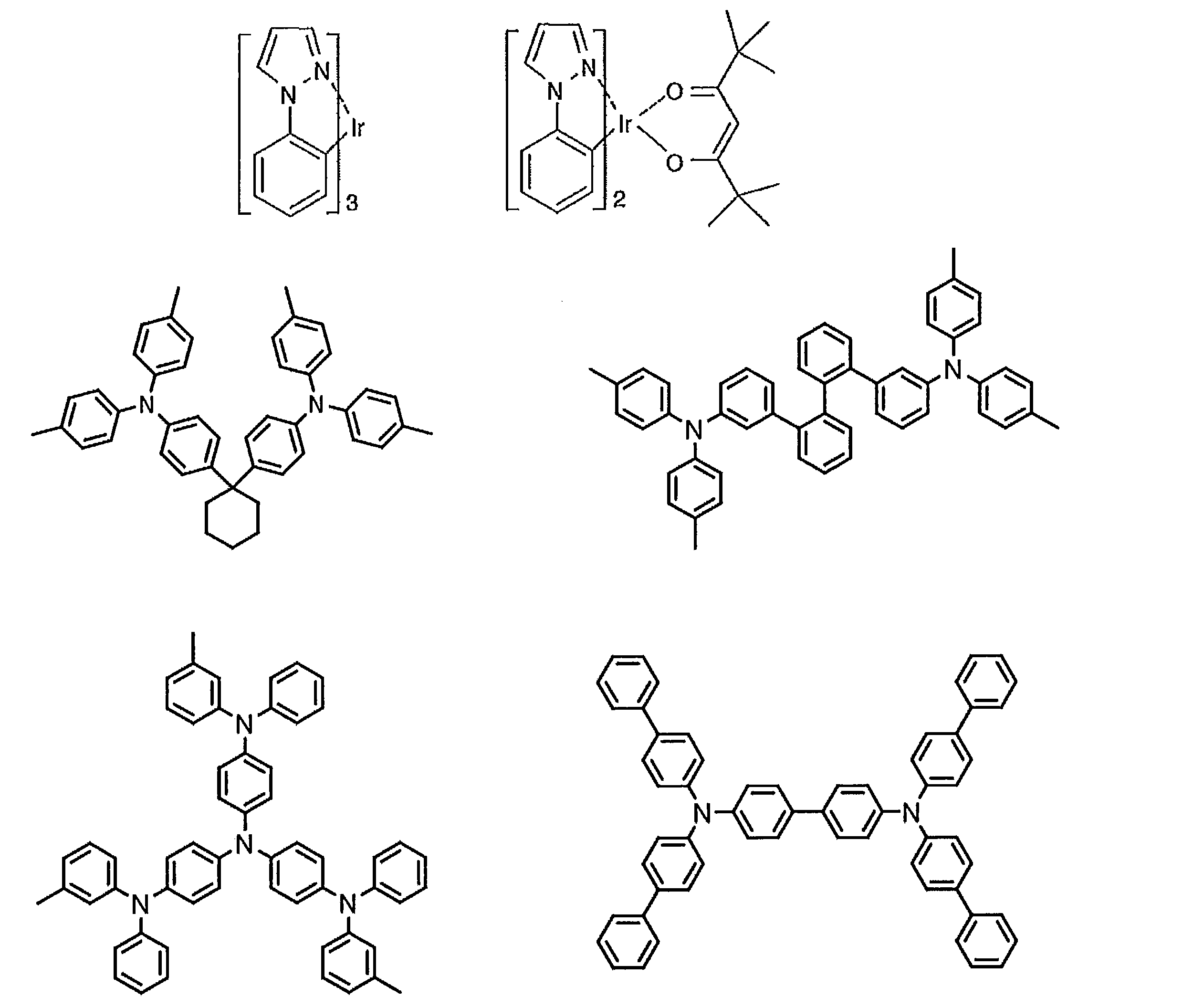
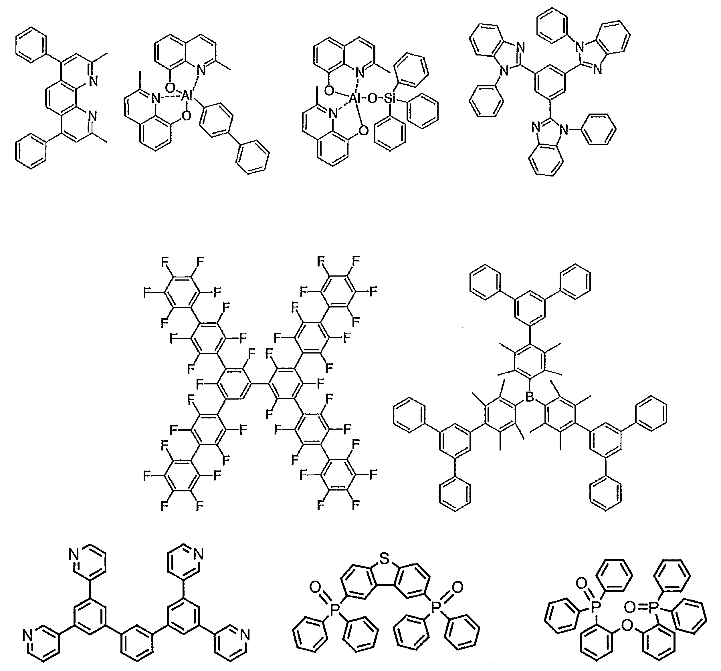

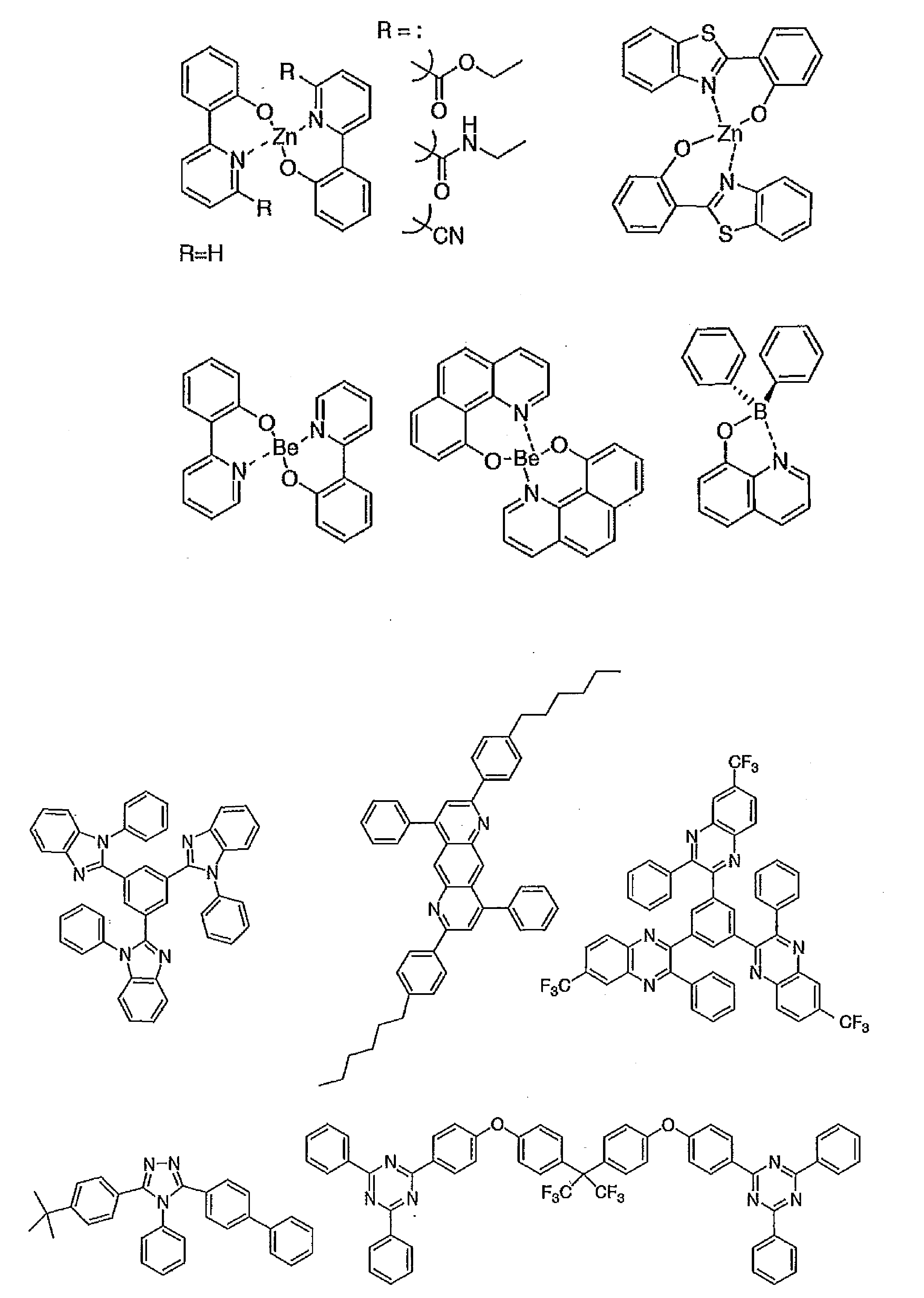
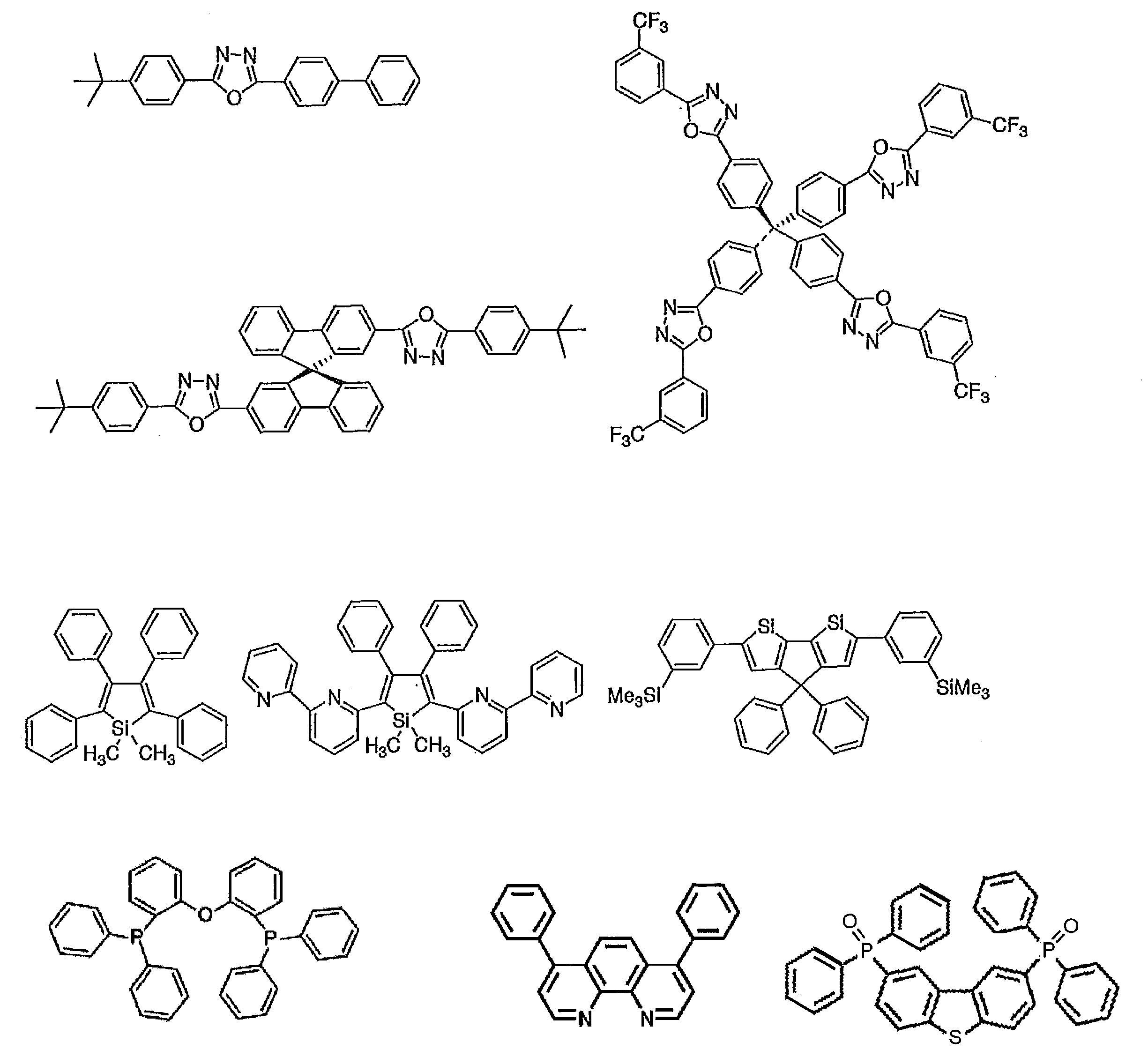
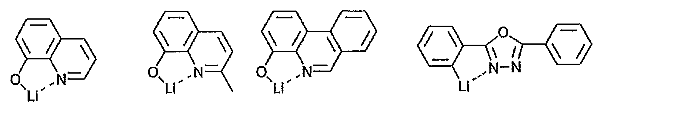
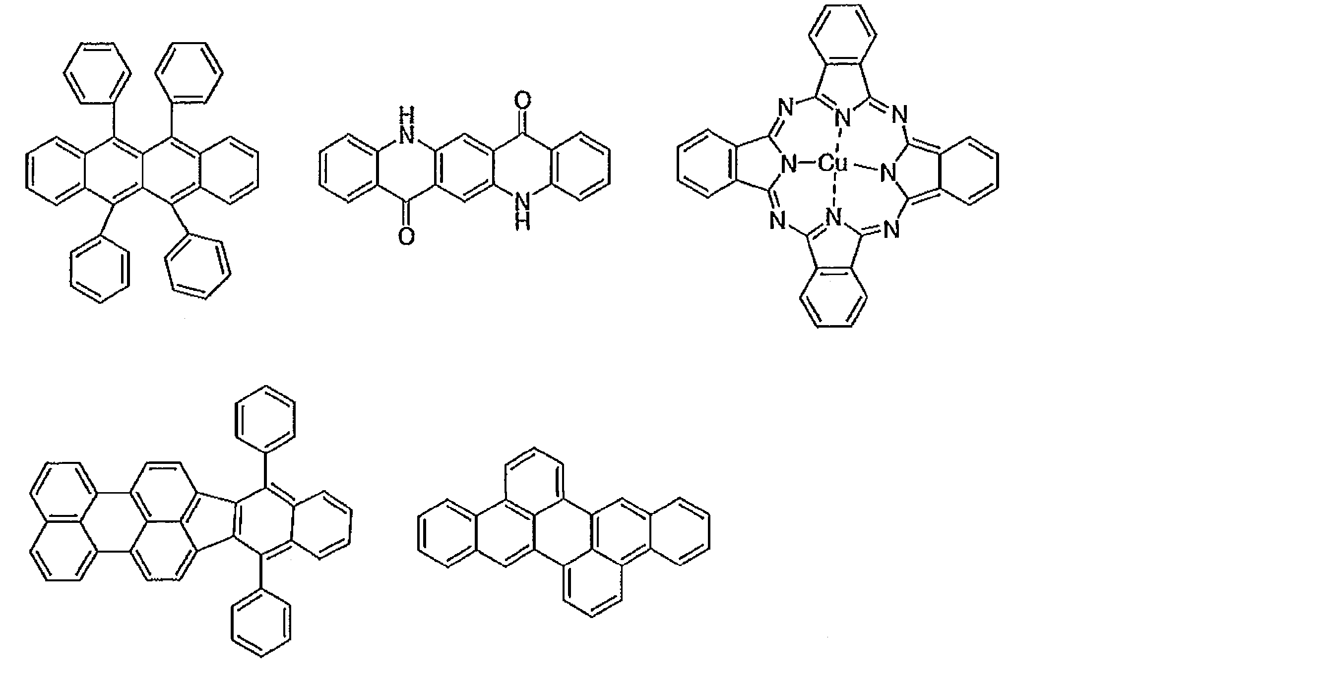
一方、りん光については、本発明の化合物のような通常の有機化合物では、励起三重項エネルギーは不安定で熱等に変換され、寿命が短く直ちに失活するため、室温では殆ど観測できない。通常の有機化合物の励起三重項エネルギーを測定するためには、極低温の条件での発光を観測することにより測定可能である。
本合成例において、化合物3を以下の手順にしたがって合成した。
ビス(4-tert-ブチルフェニル)アミン(4.22g,15mmol)を、水素化ナトリウム(0.72g,30mmol)の脱水N,N-ジメチルホルムアミド(DMF:30mL)溶液中に添加した。得られた溶液を室温で30分間攪拌して、ビス(p-フルオロフェニル)スルホン(1.91g,7.5mmol)の脱水DMF(30mL)溶液を添加した。その後、さらに100℃で1時間攪拌した後、冷却して400mlの水に注いだ。生成した白色固体をろ過して乾燥し、得られた粗生成物をさらにクロロホルムとエチルエーテルで再結晶して白色結晶4.5gを得た(収率77%)
1H NMR (CDCl3, 500 MHz): δ [ppm] 7.64(d, J = 9.0 Hz, 4H), 7.31 (d, J = 8.5 Hz, 8H), 7.05 (d, J = 8.5 Hz, 8H), 6.92 (d, J = 9.0 Hz, 4H), 1.32 (s, 36H).
13C NMR (CDCl3, 125 MHz): δ [ppm].
FD-MS m/z: 776 [M+1]+.
本合成例において、化合物21を以下の手順にしたがって合成した。
合成例1のビス(4-tert-ブチルフェニル)アミンのかわりに3,6-ジーtert-ブチルカルバゾール(4.19g,15mmol)を用いたこと以外は合成例1と同様にして、粗生成物を得た。クロロホルムとメタノールで再結晶して白色結晶4.2gを得た(収率73%)
1H NMR (CDCl3, 500 MHz): δ [ppm] 8.24(d, J = 8.5 Hz, 4H), 8.13 (s, 4H), 7.81 (d, J = 9.0Hz, 4H), 7.49-7.43 (m, 8H), 1.46 (s, 36H).
13C NMR (CDCl3, 125 MHz): δ [ppm] 144.1, 143.2, 138.8, 138.3, 129.6, 126.6, 124.1, 124.0, 116.5, 109.2, 34.8, 31.9.
FD-MS m/z: 772 [M+1]+.
本合成例において、化合物22を以下の手順にしたがって合成した。
合成例1のビス(4-tert-ブチルフェニル)アミンのかわりに3,6-ジメトキシ-9H-カルバゾール(3.41g,15mmol)を用いたこと以外は合成例1と同様にして、粗生成物を得た。クロロホルムとメタノールで再結晶して淡黄色結晶3.3gを得た(収率65%)
FD-MS m/z: 668 [M+1]+.
本合成例において、化合物355を以下の手順にしたがって合成した。
合成例1のビス(4-tert-ブチルフェニル)アミンのかわりにフェノキサジン(2.75g,15mmol)を用いたこと以外は合成例1と同様にして、粗生成物を得た。粗生成物を昇華生成して鮮黄色結晶2.4gを得た(収率55%)
FD-MS m/z: 580 [M+1]+.
合成例1~4と同様の手順にしたがって、化合物364、化合物367、化合物370、化合物373、化合物376、化合物406の各化合物を合成した。
化合物367:1H NMR (CDCl3, 500 MHz): δ [ppm] 8.44 (d, J = 8.5 Hz, 4H), 8.29 (d, J = 2.0 Hz, 4H), 8.15 (d, J = 8.5 Hz, 8H), 8.03 (d, J = 8.5 Hz, 4H), 7.76 (d, J = 8.5 Hz, 4H), 7.65 (dd, J = 8.5Hz, 2.0 Hz, 4H), 7.42-7.32 (m, 16H), 7.31-7.27 (m, 8H)
化合物370:1H NMR (CDCl3, 500 MHz): δ [ppm] 8.36 (d, J = 8.5 Hz, 4H), 8.27 (d, J = 2.0 Hz, 2H), 8.18 (d, J = 2.0 Hz, 4H), 8.10 (d, J = 8.5 Hz, 2H), 7.93 (d, J=8.5 Hz, 4H), 7.67 (d, 8.5 Hz, 2H), 7.60-7.54 (m, 4H), 7.54-7.44 (m, 6H), 7.40-7.29 (m, 6H), 1.47 (s, 36H).
化合物373:1H NMR (CDCl3, 500 MHz): δ [ppm] 8.44 (d, J = 2.0 Hz, 4H), 8.39 (d, J = 8.5 Hz, 4H), 8.35 (d, J = 2.0 Hz, 2H), 8.15 (d, J = 8.5 Hz, 2H), 7.95 (d, J = 8.5 Hz, 4H), 7.77-7.71 (m, 8H), 7.69 (dd, 8.5 Hz, 2.0 Hz, 4H), 7.63 (dd, 8.5 Hz, 2.0 Hz, 2H), 7.57 (d, 8.5 Hz, 2H), 7.52 (dd, 8.5 Hz, 2.0 Hz, 2H), 7.51-7.45 (m, 12H), 7.42-7.33 (m, 6H).
化合物376:1H NMR (CDCl3, 500 MHz): δ [ppm] 8.38 (m, 6H), 8.32 (d, J = 2.0 Hz, 2H), 8.21-8.13 (m, 8H), 7.95 (d, J = 8.5 Hz, 4H), 7.75 (d, J = 8.5 Hz, 2H), 7.67 (dd, J = 8.5Hz, 2.0Hz, 2H), 7.60-7.50 (m, 8H), 7.50-7.36 (m, 14H), 7.35-7.28 (m, 6H).
本合成例において、化合物453を以下の手順にしたがって合成した。
9,9-ジメチル-9,10-ジヒドロアクリジン(3.14g,15mmol)を、水素化ナトリウム(0.72g,30mmol)の脱水N,N-ジメチルホルムアミド(DMF:30mL)溶液中に添加した。得られた溶液を室温で30分間攪拌して、ビス(p-フルオロフェニル)スルホン(1.91g,7.5mmol)の脱水DMF(30mL)溶液を添加した。その後、さらに50℃で1時間攪拌した後、冷却して400mlの水に注いだ。生成した黄色固体をろ過して乾燥し、得られた粗生成物をさらにクロロホルムとエチルエーテルで再結晶して淡黄色結晶3.8gを得た(収率80%)
1H NMR (CDCl3, 500 MHz): δ [ppm] 8.24 (d, J = 8.5 Hz, 4H), 7.57 (d, J = 9.0 Hz, 4H), 7.48 (d, J = 8.0 Hz, 4H), 6.99-7.03 (m, 8H), 6.35 (d, J = 8.0 Hz, 4H), 1.67 (s, 12H).
本実施例において、化合物18とホスト材料からなる発光層を有する有機フォトルミネッセンス素子を作製して、特性を評価した。
シリコン基板上に真空蒸着法にて、真空度5.0×10⁻⁴Paの条件にて化合物18とDPEPOとを異なる蒸着源から蒸着し、化合物18の濃度が10重量%である薄膜を100nmの厚さで形成して有機フォトルミネッセンス素子とした。浜松ホトニクス(株)製C9920-02型絶対量子収率測定装置を用いて、N2レーザーにより337nmの光を照射した際の薄膜からの発光スペクトルを300Kで特性評価した。時間分解スペクトルの評価を、浜松ホトニクス(株)製C4334型ストリークカメラを用いて行ったところ、図2に示すように、発光寿命が短い蛍光の他に発光寿命が長い遅延蛍光が観測された。この遅延蛍光の寿命は真空中で大幅に長くなることが確認された。図3に、蛍光と遅延蛍光のストリークイメージを示す。
本実施例において、化合物18とホスト材料からなる発光層を有する有機エレクトロルミネッセンス素子を作製して、特性を評価した。
膜厚100nmのインジウム・スズ酸化物(ITO)からなる陽極が形成されたガラス基板上に、各薄膜を真空蒸着法にて、真空度5.0×10⁻⁴Paで積層した。まず、ITO上にα-NPDを40nmの厚さに形成し、その上にmCPを10nmの厚さに形成した。次に、化合物18とDPEPOを異なる蒸着源から共蒸着し、20nmの厚さの層を形成して発光層とした。この時、化合物18の濃度は6.0重量%とした。次に、DPEPOを10nmの厚さに形成し、その上にTPBIを30nmの厚さで形成した。さらにフッ化リチウム(LiF)を0.5nm真空蒸着し、次いでアルミニウム(Al)を80nmの厚さに蒸着することにより陰極を形成し、有機エレクトロルミネッセンス素子とした。
製造した有機エレクトロルミネッセンス素子を、半導体パラメータ・アナライザ(アジレント・テクノロジー社製:E5273A)、光パワーメータ測定装置(ニューポート社製:1930C)、および光学分光器(オーシャンオプティクス社製:USB2000)を用いて測定した。発光スペクトルを図4に示し、電流密度-電圧-輝度特性を図5に示し、電流密度-外部量子効率特性を図6に示す。化合物18を発光材料として用いた有機エレクトロルミネッセンス素子は3.2%の外部量子効率を達成した。
実施例1の化合物18のかわりに化合物1、化合物3、化合物21、化合物22、化合物230および化合物355を用いて有機フォトルミネッセンス素子を作製して、特性を評価した。その結果、発光寿命が短い蛍光の他に発光寿命が長い遅延蛍光が観測された。図7~11に発光スペクトルを示す。図12~17にストリークイメージを示し、図18および図19にPL過渡減衰を示す。
実施例1の化合物18のかわりに化合物21を用いて有機エレクトロルミネッセンス素子を作製して、特性を評価した。発光スペクトルを図20に示し、電流密度-電圧-輝度特性を図21に示し、電流密度-外部量子効率特性を図22に示す。化合物24を発光材料として用いた有機エレクトロルミネッセンス素子は6.7%の高い外部量子効率を達成した。
本実施例において、化合物1とホスト材料からなる発光層を有する有機エレクトロルミネッセンス素子を作製した。
膜厚100nmのインジウム・スズ酸化物(ITO)からなる陽極が形成されたガラス基板上に、各薄膜を真空蒸着法にて、真空度5.0×10⁻⁴Paで積層した。まず、ITO上にα-NPDを30nmの厚さに形成し、その上にTCTA(4、4’、4”-トリス(N-カルバゾリル)-トリフェニルアミン)を20nmの厚さに形成し、さらにその上にCzSiを10nmの厚さに形成した。次に、化合物1とDPEPOを異なる蒸着源から共蒸着し、20nmの厚さの層を形成して発光層とした。この時、化合物1の濃度は6.0重量%とした。次に、DPEPOを10nmの厚さに形成し、その上にTPBIを30nmの厚さで形成した。さらにフッ化リチウム(LiF)を0.5nm真空蒸着し、次いでアルミニウム(Al)を80nmの厚さに蒸着することにより陰極を形成し、有機エレクトロルミネッセンス素子とした。
化合物1のかわりに化合物3、化合物21およびIr(fppz)2(dfbdp)を用いて,同様にして有機エレクトロルミネッセンス素子を作製した。
作製した各有機エレクトロルミネッセンス素子について、実施例2と同じ方法により測定を行った。図23および24に電流密度-外部量子効率特性を示す。また、電流密度-電圧-輝度特性を図25に示す。
実施例5の化合物1(6.0重量%)のかわりに化合物22(10.0重量%)を使用した以外は実施例5と同様にして有機エレクトロルミネッセンス素子を作製して、同様に特性を評価した。図10に発光スペクトルを示し、電流密度-外部量子効率特性を図26に示し、電流密度-電圧-輝度特性を図27に示す。
本実施例において、化合物355とホスト材料からなる発光層を有する有機エレクトロルミネッセンス素子を作製して、特性を評価した。
膜厚100nmのインジウム・スズ酸化物(ITO)からなる陽極が形成されたガラス基板上に、各薄膜を真空蒸着法にて、真空度5.0×10⁻⁴Paで積層した。まず、ITO上にα-NPDを40nmの厚さに形成し、その上に化合物355とCBPを異なる蒸着源から共蒸着し、20nmの厚さの層を形成して発光層とした。この時、化合物355の濃度は10.0重量%とした。次に、TPBIを60nmの厚さに形成し、さらにフッ化リチウム(LiF)を0.5nm真空蒸着し、次いでアルミニウム(Al)を80nmの厚さに蒸着することにより陰極を形成し、有機エレクトロルミネッセンス素子とした。
図11に発光スペクトルを示し、電流密度-外部量子効率特性を図28に示し、電流密度-電圧-輝度特性を図29に示す。
本実施例において、化合物364、化合物367、化合物370、化合物373、化合物376の各化合物のトルエン溶液(濃度10-5mol/L)を調製して蛍光スペクトルを測定した。結果を図30~34に順に示す。
本実施例において、化合物364、化合物367、化合物370、化合物373、化合物376の各化合物とホスト材料からなる発光層を有する有機フォトルミネッセンス素子を作製して、特性を評価した。具体的な手順は、実施例1と同じであり、実施例1の化合物18のかわりに化合物364、化合物367、化合物370、化合物373、化合物376の各化合物を用いて作成した。ただし、各化合物の濃度は6重量%とした。各化合物を用いた有機フォトルミネッセンス素子では、いずれも発光寿命が短い蛍光の他に発光寿命が長い遅延蛍光が観測された。実施例1と同様にして取得した時間分解スペクトルを図35~39に順に示す。遅延蛍光の寿命は真空中で大幅に長くなることが確認された。化合物364、化合物367、化合物370のΔEST(最も短波長で発光する発光材料における、77°Kの最低励起三重項エネルギー準位と最低励起一重項エネルギー準位のエネルギー差)、遅延蛍光成分の寿命(τDLAYED)、発光量子効率(PLQE)、通常の蛍光成分の発光量子効率(PLQEPROMPT)、通常の蛍光成分の寿命(τPROMPT)を、化合物21を用いた場合の結果とともに以下の表に示す。

本実施例において、化合物21と化合物370の各化合物とホスト材料からなる発光層を有する有機エレクトロルミネッセンス素子を作製した。
膜厚100nmのインジウム・スズ酸化物(ITO)からなる陽極が形成されたガラス基板上に、各薄膜を真空蒸着法にて、真空度5.0×10⁻⁴Paで積層した。まず、ITO上にα-NPDを35nmの厚さに形成し、その上にmCBPを10nmの厚さに形成した。次に、化合物21または化合物370とDPEPOとを異なる蒸着源から共蒸着し、15nmの厚さの層を形成して発光層とした。この時、化合物21または化合物370の濃度は12.0重量%とした。次に、DPEPOを10nmの厚さに形成し、その上にTPBIを40nmの厚さで形成した。さらにフッ化リチウム(LiF)を0.5nm真空蒸着し、次いでアルミニウム(Al)を80nmの厚さに蒸着することにより陰極を形成し、有機エレクトロルミネッセンス素子とした。
作製した各有機エレクトロルミネッセンス素子について、実施例2と同じ方法により測定を行った。図40に発光スペクトルを示し、図41に電流密度-外部量子効率特性を示す。化合物370を用いた有機エレクトロルミネッセンス素子は、11%の外部量子効率を達成した。
本実施例において、化合物21と化合物406の各化合物とホスト材料からなる発光層を有する有機フォトルミネッセンス素子を作製して、特性を評価した。具体的な手順は、実施例1と同じであり、実施例1の化合物18のかわりに化合物21と化合物406の各化合物を用いて作成した。ただし、各化合物の濃度は6重量%とした。実施例1と同様にして取得した時間分解スペクトルを図42に示す。化合物406はより安定性が高いことが確認された。一方、化合物21はより発光量子効率が高いことが確認された。
本実施例において、化合物453とホスト材料からなる発光層を有する有機フォトルミネッセンス素子を作製して、特性を評価した。具体的な手順は、実施例1と同じであり、実施例1の化合物18のかわりに化合物453を用いて作成した(濃度10重量%)。実施例1と同様にして取得した発光スペクトルを図43に示し、300Kにおけるストリークイメージを図44に示し、77Kにおける発光スペクトルを図45に示す。11nsの短寿命蛍光成分と、2.8μsの長寿命蛍光成分が観測され、窒素下における発光量子収率は90%、ΔESTは0.10eVであった。
本実施例において、化合物453とホスト材料からなる発光層を有する有機エレクトロルミネッセンス素子を作製した。
膜厚100nmのインジウム・スズ酸化物(ITO)からなる陽極が形成されたガラス基板上に、各薄膜を真空蒸着法にて、真空度5.0×10⁻⁴Paで積層した。まず、ITO上にα-NPDを30nmの厚さに形成し、その上にTCTAを20nmの厚さに形成し、さらにその上にCzSiを10nmの厚さに形成した。次に、化合物453とDPEPOを異なる蒸着源から共蒸着し、20nmの厚さの層を形成して発光層とした。この時、化合物453の濃度は10.0重量%とした。次に、DPEPOを10nmの厚さに形成し、その上にTPBIを30nmの厚さで形成した。さらにフッ化リチウム(LiF)を0.5nm真空蒸着し、次いでアルミニウム(Al)を80nmの厚さに蒸着することにより陰極を形成し、有機エレクトロルミネッセンス素子とした。
化合物453のかわりにFlrpicを用いて,同様にして有機エレクトロルミネッセンス素子を作製した。
作製した各有機エレクトロルミネッセンス素子について、実施例2と同じ方法により測定を行った。図46に発光スペクトルを示し、図47に電流密度-外部量子効率特性を示す。化合物453を用いた有機エレクトロルミネッセンス素子は、19.5%の外部量子効率を達成した。


2 陽極
3 正孔注入層
4 正孔輸送層
5 発光層
6 電子輸送層
7 陰極
Claims (17)
- 下記一般式(1)で表される化合物からなる発光材料。

[一般式(1)において、R1~R10は、各々独立に水素原子または置換基を表すが、R1~R10のうちの少なくとも1つは置換もしくは無置換のアリール基、置換もしくは無置換のジアリールアミノ基、または置換もしくは無置換の9-カルバゾリル基である。R1とR2、R2とR3、R3とR4、R4とR5、R5とR6、R6とR7、R7とR8、R8とR9、R9とR10は、それぞれ互いに結合して環状構造を形成してもよい。] - 前記一般式(1)で表される化合物が、下記一般式(2)で表される構造を有することを特徴とする請求項1に記載の発光材料。

- 前記一般式(1)で表される化合物が、下記一般式(3)で表される構造を有することを特徴とする請求項1に記載の発光材料。
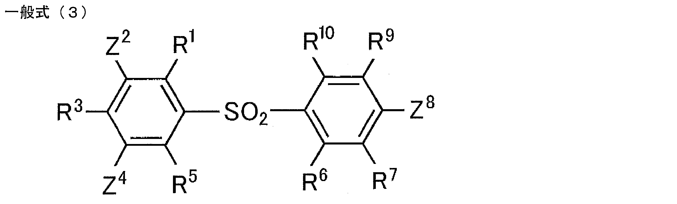
[一般式(3)において、R1、R3、R5~R7、R9、R10は、各々独立に水素原子または置換基を表す。Z2、Z4およびZ8は各々独立に水素原子、置換もしくは無置換のアリール基、置換もしくは無置換のジアリールアミノ基、または置換もしくは無置換の9-カルバゾリル基を表すが、すべてが水素原子であることはない。R5とR6、R6とR7、R9とR10は、それぞれ互いに結合して環状構造を形成してもよい。] - 前記一般式(1)で表される化合物が、下記一般式(4)で表される構造を有することを特徴とする請求項1に記載の発光材料。
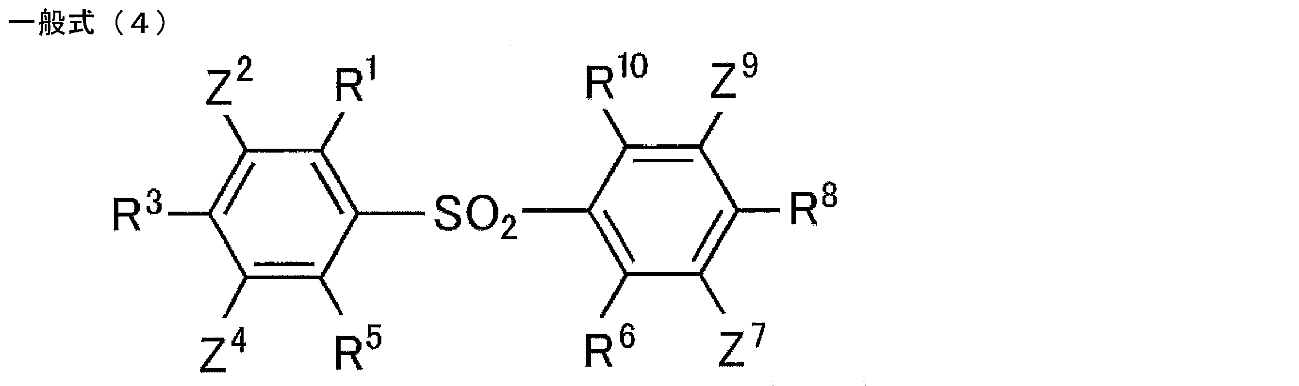
- 前記一般式(1)で表される化合物が、下記一般式(5)で表される構造を有することを特徴とする請求項1に記載の発光材料。

- 前記一般式(1)において、R1~R10が、各々独立に水素原子、置換もしくは無置換のアルキル基、または置換もしくは無置換のアルコキシ基、置換もしくは無置換のアリール基、置換もしくは無置換のジアリールアミノ基、または置換もしくは無置換の9-カルバゾリル基を表し、R1~R10のうちの少なくとも1つが置換もしくは無置換のアリール基、置換もしくは無置換のジアリールアミノ基、または置換もしくは無置換の9-カルバゾリル基であることを特徴とする請求項1~5のいずれか一項に記載の発光材料。
- 前記一般式(1)において、R1~R10が、各々独立に水素原子、置換もしくは無置換のアルキル基、または置換もしくは無置換のアルコキシ基、置換もしくは無置換のジアリールアミノ基、または置換もしくは無置換の9-カルバゾリル基を表し、R1~R10のうちの少なくとも1つが置換もしくは無置換のジアリールアミノ基、または置換もしくは無置換の9-カルバゾリル基であることを特徴とする請求項1~5のいずれか一項に記載の発光材料。
- 前記一般式(1)において、R1~R10が、各々独立に水素原子、置換もしくは無置換のジアリールアミノ基、または置換もしくは無置換の9-カルバゾリル基を表し、R1~R10のうちの少なくとも1つが置換もしくは無置換のジアリールアミノ基、または置換もしくは無置換の9-カルバゾリル基であることを特徴とする請求項1~5のいずれか一項に記載の発光材料。
- 前記一般式(1)において、R1~R10のうちの少なくとも1つが下記一般式(6)で表される構造を有することを特徴とする請求項1~8のいずれか一項に記載の発光材料。

- 前記一般式(1)において、R1~R10のうちの少なくとも1つが下記一般式(7)で表される構造を有することを特徴とする請求項1~8のいずれか一項に記載の発光材料。

- 前記一般式(1)において、R1~R10のうちの少なくとも1つが下記一般式(8)で表される構造を有することを特徴とする請求項1~8のいずれか一項に記載の発光材料。

- 前記一般式(1)において、R1~R10のうちの少なくとも1つが下記一般式(9)で表される構造を有することを特徴とする請求項1~8のいずれか一項に記載の発光材料。

- 請求項1~11のいずれか1項に記載の発光材料からなる遅延蛍光体。
- 請求項1~11のいずれか1項に記載の発光材料を含む発光層を基板上に有することを特徴とする有機発光素子。
- 遅延蛍光を放射することを特徴とする請求項14に記載の有機発光素子。
- 有機エレクトロルミネッセンス素子であることを特徴とする請求項14または15に記載の有機発光素子。
- 下記一般式(1’)で表される化合物。

Priority Applications (4)
| Application Number | Priority Date | Filing Date | Title |
|---|---|---|---|
| CN201380021890.8A CN104271701A (zh) | 2012-04-25 | 2013-03-15 | 发光材料和有机发光元件 |
| US14/396,418 US20150141642A1 (en) | 2012-04-25 | 2013-03-15 | Light-emitting material and organic light-emitting device |
| EP13782133.6A EP2862913A1 (en) | 2012-04-25 | 2013-03-15 | Light-emitting material and organic light-emitting element |
| KR1020147032505A KR20150016242A (ko) | 2012-04-25 | 2013-03-15 | 발광 재료 및 유기 발광 소자 |
Applications Claiming Priority (6)
| Application Number | Priority Date | Filing Date | Title |
|---|---|---|---|
| JP2012-100124 | 2012-04-25 | ||
| JP2012100124 | 2012-04-25 | ||
| JP2012-138055 | 2012-06-19 | ||
| JP2012138055 | 2012-06-19 | ||
| JP2012188573 | 2012-08-29 | ||
| JP2012-188573 | 2012-08-29 |
Publications (1)
| Publication Number | Publication Date |
|---|---|
| WO2013161437A1 true WO2013161437A1 (ja) | 2013-10-31 |
Family
ID=49482774
Family Applications (1)
| Application Number | Title | Priority Date | Filing Date |
|---|---|---|---|
| PCT/JP2013/057434 WO2013161437A1 (ja) | 2012-04-25 | 2013-03-15 | 発光材料および有機発光素子 |
Country Status (7)
| Country | Link |
|---|---|
| US (1) | US20150141642A1 (ja) |
| EP (1) | EP2862913A1 (ja) |
| JP (1) | JPWO2013161437A1 (ja) |
| KR (1) | KR20150016242A (ja) |
| CN (1) | CN104271701A (ja) |
| TW (1) | TW201343874A (ja) |
| WO (1) | WO2013161437A1 (ja) |
Cited By (59)
| Publication number | Priority date | Publication date | Assignee | Title |
|---|---|---|---|---|
| WO2014157619A1 (ja) | 2013-03-29 | 2014-10-02 | 国立大学法人九州大学 | 有機エレクトロルミネッセンス素子 |
| WO2015022974A1 (ja) | 2013-08-14 | 2015-02-19 | 国立大学法人九州大学 | 有機エレクトロルミネッセンス素子 |
| JP2015053476A (ja) * | 2013-07-30 | 2015-03-19 | 出光興産株式会社 | 有機エレクトロルミネッセンス素子および電子機器 |
| WO2015096226A1 (zh) * | 2013-12-26 | 2015-07-02 | 深圳市华星光电技术有限公司 | 热激活延迟荧光材料、其合成方法及使用该热激活延迟荧光材料的oled器件 |
| CN104860868A (zh) * | 2014-02-21 | 2015-08-26 | 环球展览公司 | 有机电致发光材料和装置 |
| WO2015135625A1 (de) | 2014-03-13 | 2015-09-17 | Merck Patent Gmbh | Formulierungen lumineszierender verbindungen |
| WO2015139808A1 (de) | 2014-03-18 | 2015-09-24 | Merck Patent Gmbh | Organische elektrolumineszenzvorrichtung |
| WO2016017757A1 (ja) * | 2014-07-31 | 2016-02-04 | コニカミノルタ株式会社 | 有機エレクトロルミネッセンス素子、表示装置、照明装置、π共役系化合物、発光性薄膜 |
| US9312499B1 (en) | 2015-01-05 | 2016-04-12 | Universal Display Corporation | Organic electroluminescent materials and devices |
| CN105524070A (zh) * | 2014-10-17 | 2016-04-27 | 乐金显示有限公司 | 延迟荧光化合物和使用该化合物的有机发光二极管和显示装置 |
| EP3020783A1 (en) * | 2014-11-12 | 2016-05-18 | LG Display Co., Ltd. | Delayed fluorescence compound, and organic light emitting diode and display device using the same |
| KR20160056783A (ko) * | 2014-11-12 | 2016-05-20 | 엘지디스플레이 주식회사 | 지연 형광 화합물, 이를 포함하는 유기발광다이오드소자 및 표시장치 |
| KR20160064961A (ko) * | 2014-11-28 | 2016-06-08 | 엘지디스플레이 주식회사 | 지연 형광 화합물 이를 포함하는 유기발광다이오드소자 및 표시장치 |
| CN105669526A (zh) * | 2014-11-22 | 2016-06-15 | 吉林奥来德光电材料股份有限公司 | 四苯基二苯醚类衍生物、制备方法及有机发光器件 |
| WO2016116520A1 (de) * | 2015-01-20 | 2016-07-28 | Cynora Gmbh | Phenylether-substituierte organische moleküle, insbesondere zur verwendung in optoelektronischen bauelementen |
| JP2016522579A (ja) * | 2013-06-06 | 2016-07-28 | メルク パテント ゲーエムベーハー | 有機エレクトロルミネッセント素子 |
| JP2016210910A (ja) * | 2015-05-11 | 2016-12-15 | 国立大学法人 筑波大学 | 発光材料、発光素子 |
| EP3113239A1 (de) | 2015-07-03 | 2017-01-04 | cynora GmbH | Organische moleküle zur verwendung in organischen optoelektronischen vorrichtungen |
| WO2017005699A1 (de) | 2015-07-03 | 2017-01-12 | Cynora Gmbh | Organische moleküle zur verwendung in optoelektronischen vorrichtungen |
| WO2017005698A1 (de) | 2015-07-03 | 2017-01-12 | Cynora Gmbh | Organische moleküle zur verwendung in organischen optoelektronischen vorrichtungen |
| JP2017503343A (ja) * | 2013-12-17 | 2017-01-26 | 北京維信諾科技有限公司 | 有機エレクトロルミネッセン素子及びその製造方法 |
| WO2017194435A1 (de) | 2016-05-11 | 2017-11-16 | Merck Patent Gmbh | Zusammensetzungen für elektrochemische zellen |
| EP3279193A1 (de) | 2016-08-04 | 2018-02-07 | Cynora Gmbh | Phthalimid und carbazol oder dessen analoge enthaltende verbindungen zur verwendung in organischen optoelektronischen vorrichtungen |
| EP3279194A1 (de) | 2016-08-04 | 2018-02-07 | Cynora Gmbh | Organische moleküle zur verwendung in organischen optoelektronischen vorrichtungen |
| WO2018024724A1 (de) | 2016-08-04 | 2018-02-08 | Cynora Gmbh | Organische moleküle zur verwendung in optoelektronischen vorrichtungen |
| JP2018056536A (ja) * | 2016-09-23 | 2018-04-05 | 日本放送協会 | 有機エレクトロルミネッセンス素子 |
| WO2019009307A1 (ja) * | 2017-07-03 | 2019-01-10 | 三菱ケミカル株式会社 | Oled素子形成用組成物及びoled素子 |
| JP2019085401A (ja) * | 2017-11-01 | 2019-06-06 | 東洋紡株式会社 | π電子共役単位とカルバゾール基を有する化合物 |
| KR20190098292A (ko) * | 2018-02-12 | 2019-08-22 | 삼성디스플레이 주식회사 | 유기 전계 발광 소자 및 유기 전계 발광 소자용 헤테로환 화합물 |
| US10497883B2 (en) | 2014-03-11 | 2019-12-03 | Kyulux, Inc. | Organic light-emitting device, host material, light-emitting material, and compound |
| JP2019206550A (ja) * | 2014-05-19 | 2019-12-05 | ユー・ディー・シー アイルランド リミテッド | 高い効率を有する蛍光有機発光素子 |
| US10559757B2 (en) | 2014-09-03 | 2020-02-11 | Kyulux, Inc. | Host material for delayed fluorescent materials, organic light-emitting device and compound |
| US10615348B2 (en) | 2015-11-16 | 2020-04-07 | Samsung Electronics Co., Ltd. | Organic light-emitting device |
| WO2020076796A1 (en) | 2018-10-09 | 2020-04-16 | Kyulux, Inc. | Novel composition of matter for use in organic light-emitting diodes |
| WO2020178230A1 (en) | 2019-03-04 | 2020-09-10 | Merck Patent Gmbh | Ligands for nano-sized materials |
| WO2020208051A1 (en) | 2019-04-11 | 2020-10-15 | Merck Patent Gmbh | Materials for organic electroluminescent devices |
| WO2021089450A1 (en) | 2019-11-04 | 2021-05-14 | Merck Patent Gmbh | Materials for organic electroluminescent devices |
| WO2021094269A1 (en) | 2019-11-12 | 2021-05-20 | Merck Patent Gmbh | Materials for organic electroluminescent devices |
| WO2021110741A1 (en) | 2019-12-04 | 2021-06-10 | Merck Patent Gmbh | Materials for organic electroluminescent devices |
| WO2021157593A1 (ja) | 2020-02-04 | 2021-08-12 | 株式会社Kyulux | 組成物、膜、有機発光素子、発光組成物を提供する方法およびプログラム |
| US11101440B2 (en) | 2015-07-01 | 2021-08-24 | Kyushu University, National University Corporation | Organic electroluminescent device |
| WO2021191058A1 (en) | 2020-03-23 | 2021-09-30 | Merck Patent Gmbh | Materials for organic electroluminescent devices |
| WO2021235549A1 (ja) | 2020-05-22 | 2021-11-25 | 株式会社Kyulux | 化合物、発光材料および発光素子 |
| WO2022025248A1 (ja) | 2020-07-31 | 2022-02-03 | 株式会社Kyulux | 化合物、発光材料および発光素子 |
| JP2022027942A (ja) * | 2016-05-20 | 2022-02-14 | 株式会社半導体エネルギー研究所 | 発光素子、発光装置、電子機器及び照明装置 |
| US11335872B2 (en) | 2016-09-06 | 2022-05-17 | Kyulux, Inc. | Organic light-emitting device |
| WO2022168956A1 (ja) | 2021-02-04 | 2022-08-11 | 株式会社Kyulux | 化合物、発光材料および有機発光素子 |
| US11476435B2 (en) | 2017-08-24 | 2022-10-18 | Kyushu University, National University Corporation | Film and organic light-emitting device containing perovskite-type compound and organic light-emitting material |
| US11482679B2 (en) | 2017-05-23 | 2022-10-25 | Kyushu University, National University Corporation | Compound, light-emitting lifetime lengthening agent, use of n-type compound, film and light-emitting device |
| WO2022244503A1 (ja) | 2021-05-20 | 2022-11-24 | 株式会社Kyulux | 有機発光素子 |
| WO2022270354A1 (ja) | 2021-06-23 | 2022-12-29 | 株式会社Kyulux | 化合物、発光材料および有機発光素子 |
| WO2022270602A1 (ja) | 2021-06-23 | 2022-12-29 | 株式会社Kyulux | 有機発光素子および膜 |
| WO2023282224A1 (ja) | 2021-07-06 | 2023-01-12 | 株式会社Kyulux | 有機発光素子およびその設計方法 |
| WO2023036976A1 (en) | 2021-09-13 | 2023-03-16 | Merck Patent Gmbh | Materials for organic electroluminescent devices |
| WO2023053835A1 (ja) | 2021-09-28 | 2023-04-06 | 株式会社Kyulux | 化合物、組成物、ホスト材料、電子障壁材料および有機発光素子 |
| WO2023171761A1 (ja) * | 2022-03-10 | 2023-09-14 | 国立大学法人京都大学 | ジカルバゾリル類化合物及び有機エレクトロルミネッセンス素子 |
| WO2024033282A1 (en) | 2022-08-09 | 2024-02-15 | Merck Patent Gmbh | Materials for organic electroluminescent devices |
| US11930654B2 (en) | 2017-07-06 | 2024-03-12 | Kyulux, Inc. | Organic light-emitting element |
| US11957043B2 (en) | 2020-05-06 | 2024-04-09 | Samsung Display Co., Ltd. | Light-emitting device and electronic apparatus comprising same |
Families Citing this family (51)
| Publication number | Priority date | Publication date | Assignee | Title |
|---|---|---|---|---|
| KR102081595B1 (ko) * | 2012-08-16 | 2020-02-26 | 엘지디스플레이 주식회사 | 인광 호스트 물질 및 이를 이용하는 유기전계발광소자 |
| CN103694152A (zh) * | 2013-12-20 | 2014-04-02 | 华南理工大学 | 含多甲基取代苯基悬垂侧基的二氟苯砜化合物及合成方法 |
| CN103694995B (zh) * | 2014-01-14 | 2016-02-24 | 东南大学 | 基于二苯基砜的双极蓝色磷光主体材料及制备方法和器件 |
| CN103985822B (zh) * | 2014-05-30 | 2017-05-10 | 广州华睿光电材料有限公司 | 有机混合物、包含其的组合物、有机电子器件及应用 |
| CN107109213B (zh) | 2014-12-30 | 2020-05-22 | 陶氏环球技术有限责任公司 | 作为用于电致发光装置的发光元件的芴衍生物 |
| CN104610958B (zh) * | 2015-02-06 | 2017-07-25 | 东南大学成贤学院 | 基于咔唑和二苯砜的热激活延迟荧光材料及其制备方法 |
| KR20170008358A (ko) * | 2015-07-13 | 2017-01-24 | 삼성디스플레이 주식회사 | 유기 발광 표시 장치 |
| CN105254562B (zh) * | 2015-09-01 | 2018-06-29 | 华南理工大学 | 一种有机小分子发光材料及由其制备的有机电致发光器件 |
| US11555128B2 (en) | 2015-11-12 | 2023-01-17 | Guangzhou Chinaray Optoelectronic Materials Ltd. | Printing composition, electronic device comprising same and preparation method for functional material thin film |
| CN108137634B (zh) | 2015-12-04 | 2020-11-20 | 广州华睿光电材料有限公司 | 一种金属有机配合物及其在电子器件中的应用 |
| CN105503766B (zh) * | 2015-12-18 | 2018-06-22 | 昆山国显光电有限公司 | 一种热活化延迟荧光材料及有机电致发光器件 |
| CN105647515B (zh) * | 2016-01-22 | 2017-10-20 | 华南理工大学 | 一种树枝状热活化延迟荧光材料及其合成方法 |
| KR20180015320A (ko) | 2016-08-02 | 2018-02-13 | 삼성디스플레이 주식회사 | 헤테로고리 화합물 및 이를 포함한 유기 발광 소자 |
| CN106380454A (zh) * | 2016-08-16 | 2017-02-08 | 盐城工学院 | 有机电致发光材料、发光器件及该器件的制备方法 |
| US11453745B2 (en) | 2016-11-23 | 2022-09-27 | Guangzhou Chinaray Optoelectronic Materials Ltd. | High polymer, mixture containing same, composition, organic electronic component, and monomer for polymerization |
| US11634444B2 (en) | 2016-11-23 | 2023-04-25 | Guangzhou Chinaray Optoelectronic Materials Ltd. | Metal organic complex, high polymer, composition, and organic electronic component |
| WO2018095392A1 (zh) | 2016-11-23 | 2018-05-31 | 广州华睿光电材料有限公司 | 有机混合物、组合物以及有机电子器件 |
| WO2018095389A1 (zh) | 2016-11-23 | 2018-05-31 | 广州华睿光电材料有限公司 | 含氮稠杂环的化合物及其应用 |
| CN109790407B (zh) | 2016-11-23 | 2021-12-07 | 广州华睿光电材料有限公司 | 印刷油墨组合物及其制备方法和用途 |
| US11518723B2 (en) | 2016-11-23 | 2022-12-06 | Guangzhou Chinaray Optoelectronic Materials Ltd. | Fused ring compound, high polymer, mixture, composition and organic electronic component |
| US11512039B2 (en) | 2016-11-23 | 2022-11-29 | Guangzhou Chinaray Optoelectronic Materials Ltd. | Aromatic amine derivatives, preparation methods therefor, and uses thereof |
| WO2018095388A1 (zh) | 2016-11-23 | 2018-05-31 | 广州华睿光电材料有限公司 | 有机化合物 |
| US11239428B2 (en) | 2016-11-23 | 2022-02-01 | Guangzhou Chinaray Optoelectronic Materials Ltd. | Boron-containing organic compound and applications thereof, organic mixture, and organic electronic device |
| KR20180066339A (ko) | 2016-12-07 | 2018-06-19 | 삼성디스플레이 주식회사 | 축합환 화합물 및 이를 포함한 유기 발광 소자 |
| US11672174B2 (en) | 2016-12-08 | 2023-06-06 | Guangzhou Chinaray Optoelectronic Materials Ltd. | Pyrene-triazine derivative and applications thereof in organic electronic component |
| EP3553152B1 (en) | 2016-12-08 | 2021-02-17 | Guangzhou Chinaray Optoelectronic Materials Ltd. | Mixture, composition and organic electronic device |
| US11161933B2 (en) | 2016-12-13 | 2021-11-02 | Guangzhou Chinaray Optoelectronic Materials Ltd. | Conjugated polymer and use thereof in organic electronic device |
| EP3560917B1 (en) | 2016-12-22 | 2023-12-20 | Guangzhou Chinaray Optoelectronic Materials Ltd. | Polymer containing furan crosslinking group and use thereof |
| WO2018113786A1 (zh) | 2016-12-22 | 2018-06-28 | 广州华睿光电材料有限公司 | 基于狄尔斯–阿尔德反应的可交联聚合物及其在有机电子器件中的应用 |
| KR20180097807A (ko) | 2017-02-23 | 2018-09-03 | 삼성디스플레이 주식회사 | 다환 화합물 및 이를 포함한 유기 발광 소자 |
| CN108530357A (zh) * | 2017-03-03 | 2018-09-14 | 中国科学院宁波材料技术与工程研究所 | 吖啶类d-a型热活化延迟荧光材料、其制备方法及应用 |
| US11594690B2 (en) | 2017-12-14 | 2023-02-28 | Guangzhou Chinaray Optoelectronic Materials Ltd. | Organometallic complex, and polymer, mixture and formulation comprising same, and use thereof in electronic device |
| WO2019114668A1 (zh) | 2017-12-14 | 2019-06-20 | 广州华睿光电材料有限公司 | 一种过渡金属配合物材料及其在电子器件的应用 |
| US11674080B2 (en) | 2017-12-14 | 2023-06-13 | Guangzhou Chinaray Optoelectronic Materials Ltd. | Transition metal complex, polymer, mixture, formulation and use thereof |
| CN111315721B (zh) | 2017-12-21 | 2023-06-06 | 广州华睿光电材料有限公司 | 有机混合物及其在有机电子器件中的应用 |
| CN109994628B (zh) * | 2017-12-29 | 2021-05-04 | 昆山国显光电有限公司 | 有机电致发光器件及有机电致发光器件的制备方法 |
| GB201806488D0 (en) * | 2018-04-20 | 2018-06-06 | Univ Court Univ St Andrews | Heterocyclic TADF compounds |
| CN108658940A (zh) * | 2018-07-18 | 2018-10-16 | 武汉华星光电半导体显示技术有限公司 | 热活化延迟荧光材料、其合成方法及oled发光器件 |
| CN109096159B (zh) * | 2018-08-31 | 2020-08-25 | 华南协同创新研究院 | 一类星型荧光分子及其制备方法与应用 |
| CN109943321B (zh) * | 2019-04-09 | 2021-12-07 | 南京邮电大学 | 具有延迟荧光性质的esipt发光材料及其制备方法与应用 |
| CN110272387A (zh) * | 2019-06-27 | 2019-09-24 | 武汉华星光电半导体显示技术有限公司 | 热活化延迟荧光材料、发光器件及显示面板 |
| CN110563646A (zh) * | 2019-08-27 | 2019-12-13 | 武汉华星光电半导体显示技术有限公司 | 电致发光材料、电致发光材料的制备方法及发光器件 |
| CN110511177B (zh) * | 2019-09-16 | 2022-07-26 | 南京邮电大学 | 一种d-a型tadf材料及其制备方法和应用 |
| CN111171010A (zh) * | 2020-01-13 | 2020-05-19 | 北京大学深圳研究生院 | 一种阴极电刺激响应材料及其制备方法 |
| CN111848513A (zh) * | 2020-07-28 | 2020-10-30 | 武汉大学 | 热激活延迟荧光材料及其制备方法与应用 |
| US20230345751A1 (en) | 2020-09-18 | 2023-10-26 | Samsung Display Co., Ltd. | Organic electroluminescent device |
| CN112142720B (zh) * | 2020-10-11 | 2022-12-09 | 徐州工程学院 | 基于热激活延迟荧光机制的深蓝光分子及其制备方法和应用 |
| CN112266357A (zh) * | 2020-11-09 | 2021-01-26 | 常州大学 | 具有空间电荷转移效应的荧光材料及其应用 |
| CN113429391B (zh) * | 2021-07-14 | 2022-07-19 | 山西大学 | 一种含二苯砜骨架的化合物及其制备方法和应用 |
| CN114276325B (zh) * | 2021-12-10 | 2023-05-26 | 常州大学 | 含有二苯[b, d]并噻吩-5, 5’-二氧化物有机分子材料及其应用 |
| WO2023163533A1 (ko) * | 2022-02-23 | 2023-08-31 | 삼성디스플레이주식회사 | 광전자 소자용 유기 분자 |
Citations (5)
| Publication number | Priority date | Publication date | Assignee | Title |
|---|---|---|---|---|
| JPH05224439A (ja) | 1992-02-12 | 1993-09-03 | Fuji Electric Co Ltd | 電子写真用感光体 |
| JP2000021572A (ja) * | 1998-07-06 | 2000-01-21 | Mitsubishi Chemicals Corp | 有機電界発光素子 |
| JP2002167579A (ja) * | 2000-09-25 | 2002-06-11 | Toyo Ink Mfg Co Ltd | 有機エレクトロルミネッセンス素子材料およびそれを使用した有機エレクトロルミネッセンス素子 |
| JP2004220931A (ja) | 2003-01-15 | 2004-08-05 | Mitsubishi Chemicals Corp | 有機電界発光素子 |
| JP2005089544A (ja) * | 2003-09-16 | 2005-04-07 | Toyo Ink Mfg Co Ltd | 有機エレクトロルミネッセンス素子用材料およびそれを用いた有機エレクトロルミネッセンス素子 |
Family Cites Families (3)
| Publication number | Priority date | Publication date | Assignee | Title |
|---|---|---|---|---|
| JP3274939B2 (ja) * | 1994-09-30 | 2002-04-15 | 松下電器産業株式会社 | 電界発光素子 |
| JPH10265773A (ja) * | 1997-03-24 | 1998-10-06 | Toyo Ink Mfg Co Ltd | 有機エレクトロルミネッセンス素子用正孔注入材料およびそれを使用した有機エレクトロルミネッセンス素子 |
| JP2008133225A (ja) * | 2006-11-29 | 2008-06-12 | Toyo Ink Mfg Co Ltd | インドール誘導体およびその用途 |
-
2013
- 2013-03-15 JP JP2014512416A patent/JPWO2013161437A1/ja active Pending
- 2013-03-15 WO PCT/JP2013/057434 patent/WO2013161437A1/ja active Application Filing
- 2013-03-15 EP EP13782133.6A patent/EP2862913A1/en not_active Withdrawn
- 2013-03-15 KR KR1020147032505A patent/KR20150016242A/ko not_active Application Discontinuation
- 2013-03-15 CN CN201380021890.8A patent/CN104271701A/zh active Pending
- 2013-03-15 US US14/396,418 patent/US20150141642A1/en not_active Abandoned
- 2013-03-18 TW TW102109540A patent/TW201343874A/zh unknown
Patent Citations (5)
| Publication number | Priority date | Publication date | Assignee | Title |
|---|---|---|---|---|
| JPH05224439A (ja) | 1992-02-12 | 1993-09-03 | Fuji Electric Co Ltd | 電子写真用感光体 |
| JP2000021572A (ja) * | 1998-07-06 | 2000-01-21 | Mitsubishi Chemicals Corp | 有機電界発光素子 |
| JP2002167579A (ja) * | 2000-09-25 | 2002-06-11 | Toyo Ink Mfg Co Ltd | 有機エレクトロルミネッセンス素子材料およびそれを使用した有機エレクトロルミネッセンス素子 |
| JP2004220931A (ja) | 2003-01-15 | 2004-08-05 | Mitsubishi Chemicals Corp | 有機電界発光素子 |
| JP2005089544A (ja) * | 2003-09-16 | 2005-04-07 | Toyo Ink Mfg Co Ltd | 有機エレクトロルミネッセンス素子用材料およびそれを用いた有機エレクトロルミネッセンス素子 |
Non-Patent Citations (1)
| Title |
|---|
| S. TOKITO; C. ADACHI; H. MURATA: "Yuki EL Display", OHMSHA, LTD. |
Cited By (92)
| Publication number | Priority date | Publication date | Assignee | Title |
|---|---|---|---|---|
| US10600983B2 (en) | 2013-03-29 | 2020-03-24 | Kyulux, Inc. | Organic electroluminescent device comprising delayed fluorescent materials |
| WO2014157619A1 (ja) | 2013-03-29 | 2014-10-02 | 国立大学法人九州大学 | 有機エレクトロルミネッセンス素子 |
| JP2016522579A (ja) * | 2013-06-06 | 2016-07-28 | メルク パテント ゲーエムベーハー | 有機エレクトロルミネッセント素子 |
| JP2015053476A (ja) * | 2013-07-30 | 2015-03-19 | 出光興産株式会社 | 有機エレクトロルミネッセンス素子および電子機器 |
| EP3706182A1 (en) | 2013-08-14 | 2020-09-09 | Kyushu University National University Corporation | Organic electroluminescent device |
| WO2015022974A1 (ja) | 2013-08-14 | 2015-02-19 | 国立大学法人九州大学 | 有機エレクトロルミネッセンス素子 |
| US11944010B2 (en) | 2013-08-14 | 2024-03-26 | Kyulux, Inc. | Organic electroluminescent device |
| EP4152910A1 (en) | 2013-08-14 | 2023-03-22 | Kyulux, Inc. | Organic electroluminescent device |
| US11450817B2 (en) | 2013-08-14 | 2022-09-20 | Kyulux, Inc. | Organic electroluminescent device |
| US10862047B2 (en) | 2013-08-14 | 2020-12-08 | Kyushu University, National University Corporation | Organic electroluminescent device |
| JP2017503343A (ja) * | 2013-12-17 | 2017-01-26 | 北京維信諾科技有限公司 | 有機エレクトロルミネッセン素子及びその製造方法 |
| WO2015096226A1 (zh) * | 2013-12-26 | 2015-07-02 | 深圳市华星光电技术有限公司 | 热激活延迟荧光材料、其合成方法及使用该热激活延迟荧光材料的oled器件 |
| US9590190B2 (en) | 2013-12-26 | 2017-03-07 | Shenzhen China Star Optoelectronics Technology Co., Ltd | Terminally activated delayed fluorescence material, a method of synthesizing the same and an OLED device using the same |
| CN104860868A (zh) * | 2014-02-21 | 2015-08-26 | 环球展览公司 | 有机电致发光材料和装置 |
| US10707423B2 (en) | 2014-02-21 | 2020-07-07 | Universal Display Corporation | Organic electroluminescent materials and devices |
| US10497883B2 (en) | 2014-03-11 | 2019-12-03 | Kyulux, Inc. | Organic light-emitting device, host material, light-emitting material, and compound |
| WO2015135625A1 (de) | 2014-03-13 | 2015-09-17 | Merck Patent Gmbh | Formulierungen lumineszierender verbindungen |
| WO2015139808A1 (de) | 2014-03-18 | 2015-09-24 | Merck Patent Gmbh | Organische elektrolumineszenzvorrichtung |
| JP2019206550A (ja) * | 2014-05-19 | 2019-12-05 | ユー・ディー・シー アイルランド リミテッド | 高い効率を有する蛍光有機発光素子 |
| CN109378396A (zh) * | 2014-07-31 | 2019-02-22 | 柯尼卡美能达株式会社 | 有机电致发光元件、显示装置、照明装置、π共轭系化合物、发光性薄膜 |
| US11329234B2 (en) | 2014-07-31 | 2022-05-10 | Merck Patent Gmbh | Organic electroluminescent element, display device, lighting device, π-conjugated compound, and light-emitting thin film |
| US10950799B2 (en) | 2014-07-31 | 2021-03-16 | Merck Patent Gmbh | Organic electroluminescent element, display device, lighting device, PI-conjugated compound, and light-emitting thin film |
| KR20170021300A (ko) * | 2014-07-31 | 2017-02-27 | 코니카 미놀타 가부시키가이샤 | 유기 일렉트로루미네센스 소자, 표시 장치, 조명 장치, π공액계 화합물, 발광성 박막 |
| CN106663742A (zh) * | 2014-07-31 | 2017-05-10 | 柯尼卡美能达株式会社 | 有机电致发光元件、显示装置、照明装置、π共轭系化合物、发光性薄膜 |
| JPWO2016017757A1 (ja) * | 2014-07-31 | 2017-05-25 | コニカミノルタ株式会社 | 有機エレクトロルミネッセンス素子、表示装置、照明装置、π共役系化合物、発光性薄膜 |
| KR102050145B1 (ko) * | 2014-07-31 | 2019-11-28 | 코니카 미놀타 가부시키가이샤 | 유기 일렉트로루미네센스 소자, 표시 장치, 조명 장치, π공액계 화합물, 발광성 박막 |
| WO2016017757A1 (ja) * | 2014-07-31 | 2016-02-04 | コニカミノルタ株式会社 | 有機エレクトロルミネッセンス素子、表示装置、照明装置、π共役系化合物、発光性薄膜 |
| US10559757B2 (en) | 2014-09-03 | 2020-02-11 | Kyulux, Inc. | Host material for delayed fluorescent materials, organic light-emitting device and compound |
| CN105524070A (zh) * | 2014-10-17 | 2016-04-27 | 乐金显示有限公司 | 延迟荧光化合物和使用该化合物的有机发光二极管和显示装置 |
| CN105524070B (zh) * | 2014-10-17 | 2018-02-06 | 乐金显示有限公司 | 延迟荧光化合物和使用该化合物的有机发光二极管和显示装置 |
| KR20160056783A (ko) * | 2014-11-12 | 2016-05-20 | 엘지디스플레이 주식회사 | 지연 형광 화합물, 이를 포함하는 유기발광다이오드소자 및 표시장치 |
| JP2016094418A (ja) * | 2014-11-12 | 2016-05-26 | エルジー ディスプレイ カンパニー リミテッド | 遅延蛍光化合物、これを含む有機発光ダイオード素子及び表示装置 |
| EP3020783A1 (en) * | 2014-11-12 | 2016-05-18 | LG Display Co., Ltd. | Delayed fluorescence compound, and organic light emitting diode and display device using the same |
| KR102519546B1 (ko) * | 2014-11-12 | 2023-04-07 | 엘지디스플레이 주식회사 | 지연 형광 화합물, 이를 포함하는 유기발광다이오드소자 및 표시장치 |
| CN105585577A (zh) * | 2014-11-12 | 2016-05-18 | 乐金显示有限公司 | 延迟荧光化合物和使用该化合物的有机发光二极管和显示装置 |
| US9954186B2 (en) | 2014-11-12 | 2018-04-24 | Lg Display Co., Ltd. | Delayed fluorescence compound, and organic light emitting diode and display device using the same |
| US10135005B2 (en) | 2014-11-12 | 2018-11-20 | Lg Display Co., Ltd. | Delayed fluorescence compound, and organic light emitting diode and display device using the same |
| US10651399B2 (en) | 2014-11-12 | 2020-05-12 | Lg Display Co., Ltd. | Delayed fluorescence compound, and organic light emitting diode and display device using the same |
| EP3431568A1 (en) * | 2014-11-12 | 2019-01-23 | LG Display Co., Ltd. | Delayed fluorescence compound |
| US10193085B2 (en) | 2014-11-12 | 2019-01-29 | Lg Display Co., Ltd. | Delayed fluorescence compound, and organic light emitting diode and display device using the same |
| CN105669526A (zh) * | 2014-11-22 | 2016-06-15 | 吉林奥来德光电材料股份有限公司 | 四苯基二苯醚类衍生物、制备方法及有机发光器件 |
| KR102544403B1 (ko) * | 2014-11-28 | 2023-06-16 | 엘지디스플레이 주식회사 | 지연 형광 화합물 이를 포함하는 유기발광다이오드소자 및 표시장치 |
| KR20160064961A (ko) * | 2014-11-28 | 2016-06-08 | 엘지디스플레이 주식회사 | 지연 형광 화합물 이를 포함하는 유기발광다이오드소자 및 표시장치 |
| US9312499B1 (en) | 2015-01-05 | 2016-04-12 | Universal Display Corporation | Organic electroluminescent materials and devices |
| WO2016116520A1 (de) * | 2015-01-20 | 2016-07-28 | Cynora Gmbh | Phenylether-substituierte organische moleküle, insbesondere zur verwendung in optoelektronischen bauelementen |
| JP2016210910A (ja) * | 2015-05-11 | 2016-12-15 | 国立大学法人 筑波大学 | 発光材料、発光素子 |
| US11101440B2 (en) | 2015-07-01 | 2021-08-24 | Kyushu University, National University Corporation | Organic electroluminescent device |
| WO2017005699A1 (de) | 2015-07-03 | 2017-01-12 | Cynora Gmbh | Organische moleküle zur verwendung in optoelektronischen vorrichtungen |
| WO2017005698A1 (de) | 2015-07-03 | 2017-01-12 | Cynora Gmbh | Organische moleküle zur verwendung in organischen optoelektronischen vorrichtungen |
| EP3113239A1 (de) | 2015-07-03 | 2017-01-04 | cynora GmbH | Organische moleküle zur verwendung in organischen optoelektronischen vorrichtungen |
| US10615348B2 (en) | 2015-11-16 | 2020-04-07 | Samsung Electronics Co., Ltd. | Organic light-emitting device |
| WO2017194435A1 (de) | 2016-05-11 | 2017-11-16 | Merck Patent Gmbh | Zusammensetzungen für elektrochemische zellen |
| JP7266664B2 (ja) | 2016-05-20 | 2023-04-28 | 株式会社半導体エネルギー研究所 | 発光素子、発光装置、電子機器及び照明装置 |
| JP2022027942A (ja) * | 2016-05-20 | 2022-02-14 | 株式会社半導体エネルギー研究所 | 発光素子、発光装置、電子機器及び照明装置 |
| WO2018024725A1 (de) | 2016-08-04 | 2018-02-08 | Cynora Gmbh | Organische moleküle zur verwendung in organischen optoelektronischen vorrichtungen |
| WO2018024724A1 (de) | 2016-08-04 | 2018-02-08 | Cynora Gmbh | Organische moleküle zur verwendung in optoelektronischen vorrichtungen |
| EP3279193A1 (de) | 2016-08-04 | 2018-02-07 | Cynora Gmbh | Phthalimid und carbazol oder dessen analoge enthaltende verbindungen zur verwendung in organischen optoelektronischen vorrichtungen |
| WO2018024723A1 (de) | 2016-08-04 | 2018-02-08 | Cynora Gmbh | Phthalimid und carbazol oder dessen analoge enthaltende verbindungen zur verwendung in organischen optoelektronischen vorrichtungen |
| EP3279194A1 (de) | 2016-08-04 | 2018-02-07 | Cynora Gmbh | Organische moleküle zur verwendung in organischen optoelektronischen vorrichtungen |
| US11335872B2 (en) | 2016-09-06 | 2022-05-17 | Kyulux, Inc. | Organic light-emitting device |
| JP2018056536A (ja) * | 2016-09-23 | 2018-04-05 | 日本放送協会 | 有機エレクトロルミネッセンス素子 |
| US11482679B2 (en) | 2017-05-23 | 2022-10-25 | Kyushu University, National University Corporation | Compound, light-emitting lifetime lengthening agent, use of n-type compound, film and light-emitting device |
| JPWO2019009307A1 (ja) * | 2017-07-03 | 2020-06-18 | 三菱ケミカル株式会社 | Oled素子形成用組成物及びoled素子 |
| WO2019009307A1 (ja) * | 2017-07-03 | 2019-01-10 | 三菱ケミカル株式会社 | Oled素子形成用組成物及びoled素子 |
| US11930654B2 (en) | 2017-07-06 | 2024-03-12 | Kyulux, Inc. | Organic light-emitting element |
| US11476435B2 (en) | 2017-08-24 | 2022-10-18 | Kyushu University, National University Corporation | Film and organic light-emitting device containing perovskite-type compound and organic light-emitting material |
| JP2019085401A (ja) * | 2017-11-01 | 2019-06-06 | 東洋紡株式会社 | π電子共役単位とカルバゾール基を有する化合物 |
| JP7165943B2 (ja) | 2017-11-01 | 2022-11-07 | 東洋紡株式会社 | π電子共役単位とカルバゾール基を有する化合物 |
| KR20190098292A (ko) * | 2018-02-12 | 2019-08-22 | 삼성디스플레이 주식회사 | 유기 전계 발광 소자 및 유기 전계 발광 소자용 헤테로환 화합물 |
| KR102633613B1 (ko) * | 2018-02-12 | 2024-02-07 | 삼성디스플레이 주식회사 | 유기 전계 발광 소자 및 유기 전계 발광 소자용 헤테로환 화합물 |
| WO2020076796A1 (en) | 2018-10-09 | 2020-04-16 | Kyulux, Inc. | Novel composition of matter for use in organic light-emitting diodes |
| WO2020178230A1 (en) | 2019-03-04 | 2020-09-10 | Merck Patent Gmbh | Ligands for nano-sized materials |
| WO2020208051A1 (en) | 2019-04-11 | 2020-10-15 | Merck Patent Gmbh | Materials for organic electroluminescent devices |
| WO2021089450A1 (en) | 2019-11-04 | 2021-05-14 | Merck Patent Gmbh | Materials for organic electroluminescent devices |
| WO2021094269A1 (en) | 2019-11-12 | 2021-05-20 | Merck Patent Gmbh | Materials for organic electroluminescent devices |
| WO2021110741A1 (en) | 2019-12-04 | 2021-06-10 | Merck Patent Gmbh | Materials for organic electroluminescent devices |
| WO2021157593A1 (ja) | 2020-02-04 | 2021-08-12 | 株式会社Kyulux | 組成物、膜、有機発光素子、発光組成物を提供する方法およびプログラム |
| WO2021157642A1 (ja) | 2020-02-04 | 2021-08-12 | 株式会社Kyulux | ホスト材料、組成物および有機発光素子 |
| WO2021191058A1 (en) | 2020-03-23 | 2021-09-30 | Merck Patent Gmbh | Materials for organic electroluminescent devices |
| US11957043B2 (en) | 2020-05-06 | 2024-04-09 | Samsung Display Co., Ltd. | Light-emitting device and electronic apparatus comprising same |
| WO2021235549A1 (ja) | 2020-05-22 | 2021-11-25 | 株式会社Kyulux | 化合物、発光材料および発光素子 |
| WO2022025248A1 (ja) | 2020-07-31 | 2022-02-03 | 株式会社Kyulux | 化合物、発光材料および発光素子 |
| WO2022168956A1 (ja) | 2021-02-04 | 2022-08-11 | 株式会社Kyulux | 化合物、発光材料および有機発光素子 |
| WO2022244503A1 (ja) | 2021-05-20 | 2022-11-24 | 株式会社Kyulux | 有機発光素子 |
| WO2022270354A1 (ja) | 2021-06-23 | 2022-12-29 | 株式会社Kyulux | 化合物、発光材料および有機発光素子 |
| WO2022270602A1 (ja) | 2021-06-23 | 2022-12-29 | 株式会社Kyulux | 有機発光素子および膜 |
| WO2023282224A1 (ja) | 2021-07-06 | 2023-01-12 | 株式会社Kyulux | 有機発光素子およびその設計方法 |
| WO2023036976A1 (en) | 2021-09-13 | 2023-03-16 | Merck Patent Gmbh | Materials for organic electroluminescent devices |
| WO2023053835A1 (ja) | 2021-09-28 | 2023-04-06 | 株式会社Kyulux | 化合物、組成物、ホスト材料、電子障壁材料および有機発光素子 |
| WO2023171761A1 (ja) * | 2022-03-10 | 2023-09-14 | 国立大学法人京都大学 | ジカルバゾリル類化合物及び有機エレクトロルミネッセンス素子 |
| WO2023170880A1 (ja) * | 2022-03-10 | 2023-09-14 | 国立大学法人京都大学 | ジカルバゾリルベンゼン類化合物及び有機エレクトロルミネッセンス素子 |
| WO2024033282A1 (en) | 2022-08-09 | 2024-02-15 | Merck Patent Gmbh | Materials for organic electroluminescent devices |
Also Published As
| Publication number | Publication date |
|---|---|
| CN104271701A (zh) | 2015-01-07 |
| JPWO2013161437A1 (ja) | 2015-12-24 |
| TW201343874A (zh) | 2013-11-01 |
| EP2862913A1 (en) | 2015-04-22 |
| KR20150016242A (ko) | 2015-02-11 |
| US20150141642A1 (en) | 2015-05-21 |
Similar Documents
| Publication | Publication Date | Title |
|---|---|---|
| WO2013161437A1 (ja) | 発光材料および有機発光素子 | |
| JP5679496B2 (ja) | 有機発光素子ならびにそれに用いる遅延蛍光材料および化合物 | |
| JP6293417B2 (ja) | 化合物、発光材料および有機発光素子 | |
| JP6318155B2 (ja) | 化合物、発光材料および有機発光素子 | |
| JP6262711B2 (ja) | 化合物、発光材料および有機発光素子 | |
| KR102087480B1 (ko) | 발광 재료, 유기 발광 소자 및 화합물 | |
| JP6225111B2 (ja) | 発光材料、化合物、およびそれらを用いた有機発光素子 | |
| JP5594750B2 (ja) | 化合物、発光材料および有機発光素子 | |
| JP6263524B2 (ja) | 化合物、発光材料および有機発光素子 | |
| JP5366106B1 (ja) | 有機発光素子ならびにそれに用いる発光材料および化合物 | |
| JP6277182B2 (ja) | 化合物、発光材料および有機発光素子 | |
| JP6367189B2 (ja) | 発光材料、有機発光素子および化合物 | |
| WO2013154064A1 (ja) | 有機発光素子ならびにそれに用いる発光材料および化合物 | |
| JP2017119663A (ja) | 化合物、発光材料および有機発光素子 | |
| JP2014009352A (ja) | 発光材料、化合物および有機発光素子 | |
| JP6647514B2 (ja) | 有機発光素子ならびにそれに用いる発光材料および化合物 | |
| WO2014126076A1 (ja) | 化合物、発光材料および有機発光素子 | |
| WO2017115834A1 (ja) | 化合物、発光材料および有機発光素子 | |
| JP2018111751A (ja) | 発光材料、化合物および有機発光素子 | |
| JP2016084283A (ja) | 化合物、発光材料および有機発光素子 | |
| JP2016084284A (ja) | 化合物、発光材料および有機発光素子 |
Legal Events
| Date | Code | Title | Description |
|---|---|---|---|
| 121 | Ep: the epo has been informed by wipo that ep was designated in this application |
Ref document number: 13782133 Country of ref document: EP Kind code of ref document: A1 |
|
| ENP | Entry into the national phase |
Ref document number: 2014512416 Country of ref document: JP Kind code of ref document: A |
|
| WWE | Wipo information: entry into national phase |
Ref document number: 14396418 Country of ref document: US |
|
| NENP | Non-entry into the national phase |
Ref country code: DE |
|
| ENP | Entry into the national phase |
Ref document number: 20147032505 Country of ref document: KR Kind code of ref document: A |
|
| WWE | Wipo information: entry into national phase |
Ref document number: 2013782133 Country of ref document: EP |