WO2023053835A1 - 化合物、組成物、ホスト材料、電子障壁材料および有機発光素子 - Google Patents
化合物、組成物、ホスト材料、電子障壁材料および有機発光素子 Download PDFInfo
- Publication number
- WO2023053835A1 WO2023053835A1 PCT/JP2022/032781 JP2022032781W WO2023053835A1 WO 2023053835 A1 WO2023053835 A1 WO 2023053835A1 JP 2022032781 W JP2022032781 W JP 2022032781W WO 2023053835 A1 WO2023053835 A1 WO 2023053835A1
- Authority
- WO
- WIPO (PCT)
- Prior art keywords
- group
- compound
- substituted
- general formula
- atoms
- Prior art date
Links
- 239000000463 material Substances 0.000 title claims abstract description 179
- 150000001875 compounds Chemical class 0.000 title claims abstract description 158
- 230000004888 barrier function Effects 0.000 title claims abstract description 46
- 239000000203 mixture Substances 0.000 title claims description 73
- 125000000217 alkyl group Chemical group 0.000 claims abstract description 113
- 125000004431 deuterium atom Chemical group 0.000 claims abstract description 90
- 125000001997 phenyl group Chemical group [H]C1=C([H])C([H])=C(*)C([H])=C1[H] 0.000 claims abstract description 74
- 230000003111 delayed effect Effects 0.000 claims description 94
- 229910052805 deuterium Inorganic materials 0.000 claims description 71
- 125000004432 carbon atom Chemical group C* 0.000 claims description 61
- 125000004435 hydrogen atom Chemical group [H]* 0.000 claims description 41
- HEDRZPFGACZZDS-UHFFFAOYSA-N Chloroform Chemical compound ClC(Cl)Cl HEDRZPFGACZZDS-UHFFFAOYSA-N 0.000 claims description 34
- 238000005401 electroluminescence Methods 0.000 claims description 33
- 125000004122 cyclic group Chemical group 0.000 claims description 29
- 125000004433 nitrogen atom Chemical group N* 0.000 claims description 21
- TXCDCPKCNAJMEE-UHFFFAOYSA-N dibenzofuran Chemical compound C1=CC=C2C3=CC=CC=C3OC2=C1 TXCDCPKCNAJMEE-UHFFFAOYSA-N 0.000 claims description 20
- 239000007850 fluorescent dye Substances 0.000 claims description 19
- 125000004093 cyano group Chemical group *C#N 0.000 claims description 16
- 125000004430 oxygen atom Chemical group O* 0.000 claims description 14
- 125000004434 sulfur atom Chemical group 0.000 claims description 12
- 125000004429 atom Chemical group 0.000 claims description 11
- JFDZBHWFFUWGJE-UHFFFAOYSA-N benzonitrile Chemical group N#CC1=CC=CC=C1 JFDZBHWFFUWGJE-UHFFFAOYSA-N 0.000 claims description 4
- 125000005843 halogen group Chemical group 0.000 claims description 4
- 125000000843 phenylene group Chemical group C1(=C(C=CC=C1)*)* 0.000 claims description 4
- XQZYPMVTSDWCCE-UHFFFAOYSA-N phthalonitrile Chemical group N#CC1=CC=CC=C1C#N XQZYPMVTSDWCCE-UHFFFAOYSA-N 0.000 claims description 4
- ZOXJGFHDIHLPTG-UHFFFAOYSA-N Boron Chemical group [B] ZOXJGFHDIHLPTG-UHFFFAOYSA-N 0.000 claims description 3
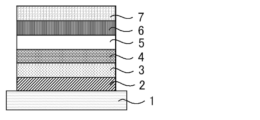
- 239000010410 layer Substances 0.000 description 208
- 239000010408 film Substances 0.000 description 63
- -1 3,5-dimethylphenyl group Chemical group 0.000 description 55
- YXFVVABEGXRONW-UHFFFAOYSA-N Toluene Chemical compound CC1=CC=CC=C1 YXFVVABEGXRONW-UHFFFAOYSA-N 0.000 description 42
- 239000000758 substrate Substances 0.000 description 39
- 230000000903 blocking effect Effects 0.000 description 32
- 125000001424 substituent group Chemical group 0.000 description 31
- 238000002347 injection Methods 0.000 description 24
- 239000007924 injection Substances 0.000 description 24
- 230000032258 transport Effects 0.000 description 24
- 125000003118 aryl group Chemical group 0.000 description 22
- 230000000052 comparative effect Effects 0.000 description 20
- JUJWROOIHBZHMG-UHFFFAOYSA-N Pyridine Chemical class C1=CC=NC=C1 JUJWROOIHBZHMG-UHFFFAOYSA-N 0.000 description 17
- 230000005525 hole transport Effects 0.000 description 17
- 238000000034 method Methods 0.000 description 17
- 125000002496 methyl group Chemical group [H]C([H])([H])* 0.000 description 17
- OKKJLVBELUTLKV-UHFFFAOYSA-N Methanol Chemical compound OC OKKJLVBELUTLKV-UHFFFAOYSA-N 0.000 description 15
- 239000012044 organic layer Substances 0.000 description 14
- 239000010409 thin film Substances 0.000 description 13
- 238000007740 vapor deposition Methods 0.000 description 13
- CYPYTURSJDMMMP-WVCUSYJESA-N (1e,4e)-1,5-diphenylpenta-1,4-dien-3-one;palladium Chemical compound [Pd].[Pd].C=1C=CC=CC=1\C=C\C(=O)\C=C\C1=CC=CC=C1.C=1C=CC=CC=1\C=C\C(=O)\C=C\C1=CC=CC=C1.C=1C=CC=CC=1\C=C\C(=O)\C=C\C1=CC=CC=C1 CYPYTURSJDMMMP-WVCUSYJESA-N 0.000 description 12
- 125000004556 carbazol-9-yl group Chemical group C1=CC=CC=2C3=CC=CC=C3N(C12)* 0.000 description 12
- 229910052751 metal Inorganic materials 0.000 description 12
- VLKZOEOYAKHREP-UHFFFAOYSA-N n-Hexane Chemical compound CCCCCC VLKZOEOYAKHREP-UHFFFAOYSA-N 0.000 description 12
- MFRIHAYPQRLWNB-UHFFFAOYSA-N sodium tert-butoxide Chemical compound [Na+].CC(C)(C)[O-] MFRIHAYPQRLWNB-UHFFFAOYSA-N 0.000 description 12
- 230000015572 biosynthetic process Effects 0.000 description 11
- 125000001072 heteroaryl group Chemical group 0.000 description 11
- 239000002184 metal Substances 0.000 description 11
- 239000007787 solid Substances 0.000 description 11
- 238000003786 synthesis reaction Methods 0.000 description 11
- 238000006243 chemical reaction Methods 0.000 description 10
- 238000005538 encapsulation Methods 0.000 description 10
- 239000002904 solvent Substances 0.000 description 10
- 125000003342 alkenyl group Chemical group 0.000 description 9
- 229940125782 compound 2 Drugs 0.000 description 9
- 239000000243 solution Substances 0.000 description 9
- CSNNHWWHGAXBCP-UHFFFAOYSA-L Magnesium sulfate Chemical compound [Mg+2].[O-][S+2]([O-])([O-])[O-] CSNNHWWHGAXBCP-UHFFFAOYSA-L 0.000 description 8
- 239000004642 Polyimide Substances 0.000 description 8
- 125000005647 linker group Chemical group 0.000 description 8
- 229920001721 polyimide Polymers 0.000 description 8
- 238000000151 deposition Methods 0.000 description 7
- NXFRHDBTYGPEDX-UHFFFAOYSA-N 2-(3-bromophenyl)dibenzofuran Chemical compound BrC1=CC=CC(C=2C=C3C4=CC=CC=C4OC3=CC=2)=C1 NXFRHDBTYGPEDX-UHFFFAOYSA-N 0.000 description 6
- 125000000609 carbazolyl group Chemical group C1(=CC=CC=2C3=CC=CC=C3NC12)* 0.000 description 6
- 238000005520 cutting process Methods 0.000 description 6
- 239000011521 glass Substances 0.000 description 6
- 238000004519 manufacturing process Methods 0.000 description 6
- 229910052757 nitrogen Inorganic materials 0.000 description 6
- 239000012299 nitrogen atmosphere Substances 0.000 description 6
- 238000001296 phosphorescence spectrum Methods 0.000 description 6
- SRKGZXIJDGWVAI-GVAVTCRGSA-M (e,3r)-7-[6-tert-butyl-4-(4-fluorophenyl)-2-propan-2-ylpyridin-3-yl]-3,5-dihydroxyhept-6-enoate Chemical compound CC(C)C1=NC(C(C)(C)C)=CC(C=2C=CC(F)=CC=2)=C1\C=C\C(O)C[C@@H](O)CC([O-])=O SRKGZXIJDGWVAI-GVAVTCRGSA-M 0.000 description 5
- NIXOWILDQLNWCW-UHFFFAOYSA-N acrylic acid group Chemical group C(C=C)(=O)O NIXOWILDQLNWCW-UHFFFAOYSA-N 0.000 description 5
- 229910052782 aluminium Inorganic materials 0.000 description 5
- 125000000732 arylene group Chemical group 0.000 description 5
- 238000000576 coating method Methods 0.000 description 5
- 239000003086 colorant Substances 0.000 description 5
- 230000005283 ground state Effects 0.000 description 5
- 125000001449 isopropyl group Chemical group [H]C([H])([H])C([H])(*)C([H])([H])[H] 0.000 description 5
- 125000001624 naphthyl group Chemical group 0.000 description 5
- 230000008569 process Effects 0.000 description 5
- 125000000714 pyrimidinyl group Chemical group 0.000 description 5
- VYPSYNLAJGMNEJ-UHFFFAOYSA-N silicon dioxide Inorganic materials O=[Si]=O VYPSYNLAJGMNEJ-UHFFFAOYSA-N 0.000 description 5
- 125000000999 tert-butyl group Chemical group [H]C([H])([H])C(*)(C([H])([H])[H])C([H])([H])[H] 0.000 description 5
- 229940126062 Compound A Drugs 0.000 description 4
- NLDMNSXOCDLTTB-UHFFFAOYSA-N Heterophylliin A Natural products O1C2COC(=O)C3=CC(O)=C(O)C(O)=C3C3=C(O)C(O)=C(O)C=C3C(=O)OC2C(OC(=O)C=2C=C(O)C(O)=C(O)C=2)C(O)C1OC(=O)C1=CC(O)=C(O)C(O)=C1 NLDMNSXOCDLTTB-UHFFFAOYSA-N 0.000 description 4
- YTPLMLYBLZKORZ-UHFFFAOYSA-N Thiophene Chemical group C=1C=CSC=1 YTPLMLYBLZKORZ-UHFFFAOYSA-N 0.000 description 4
- XAGFODPZIPBFFR-UHFFFAOYSA-N aluminium Chemical compound [Al] XAGFODPZIPBFFR-UHFFFAOYSA-N 0.000 description 4
- 239000011248 coating agent Substances 0.000 description 4
- 230000008021 deposition Effects 0.000 description 4
- 239000007772 electrode material Substances 0.000 description 4
- 238000005530 etching Methods 0.000 description 4
- 238000001704 evaporation Methods 0.000 description 4
- 230000008020 evaporation Effects 0.000 description 4
- AMGQUBHHOARCQH-UHFFFAOYSA-N indium;oxotin Chemical compound [In].[Sn]=O AMGQUBHHOARCQH-UHFFFAOYSA-N 0.000 description 4
- 238000004020 luminiscence type Methods 0.000 description 4
- 229910052943 magnesium sulfate Inorganic materials 0.000 description 4
- 235000019341 magnesium sulphate Nutrition 0.000 description 4
- 238000005259 measurement Methods 0.000 description 4
- 150000002739 metals Chemical class 0.000 description 4
- 238000002161 passivation Methods 0.000 description 4
- 238000001953 recrystallisation Methods 0.000 description 4
- 238000010898 silica gel chromatography Methods 0.000 description 4
- 238000001771 vacuum deposition Methods 0.000 description 4
- XLYOFNOQVPJJNP-UHFFFAOYSA-N water Substances O XLYOFNOQVPJJNP-UHFFFAOYSA-N 0.000 description 4
- XEKOWRVHYACXOJ-UHFFFAOYSA-N Ethyl acetate Chemical compound CCOC(C)=O XEKOWRVHYACXOJ-UHFFFAOYSA-N 0.000 description 3
- 229910001374 Invar Inorganic materials 0.000 description 3
- 229910045601 alloy Inorganic materials 0.000 description 3
- 239000000956 alloy Substances 0.000 description 3
- 238000005229 chemical vapour deposition Methods 0.000 description 3
- 238000005336 cracking Methods 0.000 description 3
- DKHNGUNXLDCATP-UHFFFAOYSA-N dipyrazino[2,3-f:2',3'-h]quinoxaline-2,3,6,7,10,11-hexacarbonitrile Chemical compound C12=NC(C#N)=C(C#N)N=C2C2=NC(C#N)=C(C#N)N=C2C2=C1N=C(C#N)C(C#N)=N2 DKHNGUNXLDCATP-UHFFFAOYSA-N 0.000 description 3
- 125000001495 ethyl group Chemical group [H]C([H])([H])C([H])([H])* 0.000 description 3
- 230000005284 excitation Effects 0.000 description 3
- 230000005281 excited state Effects 0.000 description 3
- 230000006872 improvement Effects 0.000 description 3
- 238000010030 laminating Methods 0.000 description 3
- 125000001434 methanylylidene group Chemical group [H]C#[*] 0.000 description 3
- YGBMCLDVRUGXOV-UHFFFAOYSA-N n-[6-[6-chloro-5-[(4-fluorophenyl)sulfonylamino]pyridin-3-yl]-1,3-benzothiazol-2-yl]acetamide Chemical compound C1=C2SC(NC(=O)C)=NC2=CC=C1C(C=1)=CN=C(Cl)C=1NS(=O)(=O)C1=CC=C(F)C=C1 YGBMCLDVRUGXOV-UHFFFAOYSA-N 0.000 description 3
- 230000003287 optical effect Effects 0.000 description 3
- YNPNZTXNASCQKK-UHFFFAOYSA-N phenanthrene Chemical group C1=CC=C2C3=CC=CC=C3C=CC2=C1 YNPNZTXNASCQKK-UHFFFAOYSA-N 0.000 description 3
- 125000003373 pyrazinyl group Chemical group 0.000 description 3
- 125000001567 quinoxalinyl group Chemical group N1=C(C=NC2=CC=CC=C12)* 0.000 description 3
- 230000006798 recombination Effects 0.000 description 3
- 238000005215 recombination Methods 0.000 description 3
- 125000006413 ring segment Chemical group 0.000 description 3
- 239000002356 single layer Substances 0.000 description 3
- 238000001228 spectrum Methods 0.000 description 3
- 238000004544 sputter deposition Methods 0.000 description 3
- 229910052717 sulfur Inorganic materials 0.000 description 3
- 230000007704 transition Effects 0.000 description 3
- YJTKZCDBKVTVBY-UHFFFAOYSA-N 1,3-Diphenylbenzene Chemical class C1=CC=CC=C1C1=CC=CC(C=2C=CC=CC=2)=C1 YJTKZCDBKVTVBY-UHFFFAOYSA-N 0.000 description 2
- 125000001989 1,3-phenylene group Chemical group [H]C1=C([H])C([*:1])=C([H])C([*:2])=C1[H] 0.000 description 2
- 125000001140 1,4-phenylene group Chemical group [H]C1=C([H])C([*:2])=C([H])C([H])=C1[*:1] 0.000 description 2
- FLBAYUMRQUHISI-UHFFFAOYSA-N 1,8-naphthyridine Chemical group N1=CC=CC2=CC=CN=C21 FLBAYUMRQUHISI-UHFFFAOYSA-N 0.000 description 2
- WZZBNLYBHUDSHF-DHLKQENFSA-N 1-[(3s,4s)-4-[8-(2-chloro-4-pyrimidin-2-yloxyphenyl)-7-fluoro-2-methylimidazo[4,5-c]quinolin-1-yl]-3-fluoropiperidin-1-yl]-2-hydroxyethanone Chemical compound CC1=NC2=CN=C3C=C(F)C(C=4C(=CC(OC=5N=CC=CN=5)=CC=4)Cl)=CC3=C2N1[C@H]1CCN(C(=O)CO)C[C@@H]1F WZZBNLYBHUDSHF-DHLKQENFSA-N 0.000 description 2
- UJOBWOGCFQCDNV-UHFFFAOYSA-N 9H-carbazole Chemical compound C1=CC=C2C3=CC=CC=C3NC2=C1 UJOBWOGCFQCDNV-UHFFFAOYSA-N 0.000 description 2
- PNEYBMLMFCGWSK-UHFFFAOYSA-N Alumina Chemical compound [O-2].[O-2].[O-2].[Al+3].[Al+3] PNEYBMLMFCGWSK-UHFFFAOYSA-N 0.000 description 2
- IJGRMHOSHXDMSA-UHFFFAOYSA-N Atomic nitrogen Chemical compound N#N IJGRMHOSHXDMSA-UHFFFAOYSA-N 0.000 description 2
- YLQBMQCUIZJEEH-UHFFFAOYSA-N Furan Chemical group C=1C=COC=1 YLQBMQCUIZJEEH-UHFFFAOYSA-N 0.000 description 2
- PXHVJJICTQNCMI-UHFFFAOYSA-N Nickel Chemical compound [Ni] PXHVJJICTQNCMI-UHFFFAOYSA-N 0.000 description 2
- JFBZPFYRPYOZCQ-UHFFFAOYSA-N [Li].[Al] Chemical compound [Li].[Al] JFBZPFYRPYOZCQ-UHFFFAOYSA-N 0.000 description 2
- JHYLKGDXMUDNEO-UHFFFAOYSA-N [Mg].[In] Chemical compound [Mg].[In] JHYLKGDXMUDNEO-UHFFFAOYSA-N 0.000 description 2
- 125000002252 acyl group Chemical group 0.000 description 2
- 125000003545 alkoxy group Chemical group 0.000 description 2
- 125000004453 alkoxycarbonyl group Chemical group 0.000 description 2
- 125000004414 alkyl thio group Chemical group 0.000 description 2
- 125000000304 alkynyl group Chemical group 0.000 description 2
- SNAAJJQQZSMGQD-UHFFFAOYSA-N aluminum magnesium Chemical compound [Mg].[Al] SNAAJJQQZSMGQD-UHFFFAOYSA-N 0.000 description 2
- 125000005577 anthracene group Chemical group 0.000 description 2
- 125000005161 aryl oxy carbonyl group Chemical group 0.000 description 2
- 125000005110 aryl thio group Chemical group 0.000 description 2
- 125000004104 aryloxy group Chemical group 0.000 description 2
- 150000007980 azole derivatives Chemical class 0.000 description 2
- 125000002529 biphenylenyl group Chemical group C1(=CC=CC=2C3=CC=CC=C3C12)* 0.000 description 2
- MVPPADPHJFYWMZ-UHFFFAOYSA-N chlorobenzene Chemical compound ClC1=CC=CC=C1 MVPPADPHJFYWMZ-UHFFFAOYSA-N 0.000 description 2
- 125000000582 cycloheptyl group Chemical group [H]C1([H])C([H])([H])C([H])([H])C([H])([H])C([H])(*)C([H])([H])C1([H])[H] 0.000 description 2
- 125000000113 cyclohexyl group Chemical group [H]C1([H])C([H])([H])C([H])([H])C([H])(*)C([H])([H])C1([H])[H] 0.000 description 2
- 125000001511 cyclopentyl group Chemical group [H]C1([H])C([H])([H])C([H])([H])C([H])(*)C1([H])[H] 0.000 description 2
- 238000001035 drying Methods 0.000 description 2
- 238000000295 emission spectrum Methods 0.000 description 2
- 238000002189 fluorescence spectrum Methods 0.000 description 2
- 125000005549 heteroarylene group Chemical group 0.000 description 2
- 125000005553 heteroaryloxy group Chemical group 0.000 description 2
- 125000005226 heteroaryloxycarbonyl group Chemical group 0.000 description 2
- 125000005368 heteroarylthio group Chemical group 0.000 description 2
- 125000005842 heteroatom Chemical group 0.000 description 2
- 125000000959 isobutyl group Chemical group [H]C([H])([H])C([H])(C([H])([H])[H])C([H])([H])* 0.000 description 2
- 125000001972 isopentyl group Chemical group [H]C([H])([H])C([H])(C([H])([H])[H])C([H])([H])C([H])([H])* 0.000 description 2
- SJCKRGFTWFGHGZ-UHFFFAOYSA-N magnesium silver Chemical compound [Mg].[Ag] SJCKRGFTWFGHGZ-UHFFFAOYSA-N 0.000 description 2
- 239000011812 mixed powder Substances 0.000 description 2
- 238000002156 mixing Methods 0.000 description 2
- 125000004108 n-butyl group Chemical group [H]C([H])([H])C([H])([H])C([H])([H])C([H])([H])* 0.000 description 2
- 125000001280 n-hexyl group Chemical group C(CCCCC)* 0.000 description 2
- 125000000740 n-pentyl group Chemical group [H]C([H])([H])C([H])([H])C([H])([H])C([H])([H])C([H])([H])* 0.000 description 2
- 125000004123 n-propyl group Chemical group [H]C([H])([H])C([H])([H])C([H])([H])* 0.000 description 2
- 239000003960 organic solvent Substances 0.000 description 2
- 150000004866 oxadiazoles Chemical class 0.000 description 2
- 230000037361 pathway Effects 0.000 description 2
- 238000000059 patterning Methods 0.000 description 2
- 238000005424 photoluminescence Methods 0.000 description 2
- 238000007639 printing Methods 0.000 description 2
- 238000012545 processing Methods 0.000 description 2
- 230000002035 prolonged effect Effects 0.000 description 2
- 125000004309 pyranyl group Chemical class O1C(C=CC=C1)* 0.000 description 2
- PBMFSQRYOILNGV-UHFFFAOYSA-N pyridazine Chemical group C1=CC=NN=C1 PBMFSQRYOILNGV-UHFFFAOYSA-N 0.000 description 2
- 125000002943 quinolinyl group Chemical group N1=C(C=CC2=CC=CC=C12)* 0.000 description 2
- 230000003595 spectral effect Effects 0.000 description 2
- PJANXHGTPQOBST-UHFFFAOYSA-N stilbene Chemical class C=1C=CC=CC=1C=CC1=CC=CC=C1 PJANXHGTPQOBST-UHFFFAOYSA-N 0.000 description 2
- 150000003518 tetracenes Chemical class 0.000 description 2
- XOLBLPGZBRYERU-UHFFFAOYSA-N tin dioxide Chemical compound O=[Sn]=O XOLBLPGZBRYERU-UHFFFAOYSA-N 0.000 description 2
- 239000012780 transparent material Substances 0.000 description 2
- 125000005580 triphenylene group Chemical group 0.000 description 2
- 238000003631 wet chemical etching Methods 0.000 description 2
- 125000004169 (C1-C6) alkyl group Chemical group 0.000 description 1
- UVNPEUJXKZFWSJ-LMTQTHQJSA-N (R)-N-[(4S)-8-[6-amino-5-[(3,3-difluoro-2-oxo-1H-pyrrolo[2,3-b]pyridin-4-yl)sulfanyl]pyrazin-2-yl]-2-oxa-8-azaspiro[4.5]decan-4-yl]-2-methylpropane-2-sulfinamide Chemical compound CC(C)(C)[S@@](=O)N[C@@H]1COCC11CCN(CC1)c1cnc(Sc2ccnc3NC(=O)C(F)(F)c23)c(N)n1 UVNPEUJXKZFWSJ-LMTQTHQJSA-N 0.000 description 1
- UWRZIZXBOLBCON-VOTSOKGWSA-N (e)-2-phenylethenamine Chemical class N\C=C\C1=CC=CC=C1 UWRZIZXBOLBCON-VOTSOKGWSA-N 0.000 description 1
- JYEUMXHLPRZUAT-UHFFFAOYSA-N 1,2,3-triazine Chemical group C1=CN=NN=C1 JYEUMXHLPRZUAT-UHFFFAOYSA-N 0.000 description 1
- 125000003363 1,3,5-triazinyl group Chemical group N1=C(N=CN=C1)* 0.000 description 1
- GWYPDXLJACEENP-UHFFFAOYSA-N 1,3-cycloheptadiene Chemical group C1CC=CC=CC1 GWYPDXLJACEENP-UHFFFAOYSA-N 0.000 description 1
- VERMWGQSKPXSPZ-BUHFOSPRSA-N 1-[(e)-2-phenylethenyl]anthracene Chemical class C=1C=CC2=CC3=CC=CC=C3C=C2C=1\C=C\C1=CC=CC=C1 VERMWGQSKPXSPZ-BUHFOSPRSA-N 0.000 description 1
- IANQTJSKSUMEQM-UHFFFAOYSA-N 1-benzofuran Chemical group C1=CC=C2OC=CC2=C1 IANQTJSKSUMEQM-UHFFFAOYSA-N 0.000 description 1
- FCEHBMOGCRZNNI-UHFFFAOYSA-N 1-benzothiophene Chemical group C1=CC=C2SC=CC2=C1 FCEHBMOGCRZNNI-UHFFFAOYSA-N 0.000 description 1
- 125000001637 1-naphthyl group Chemical group [H]C1=C([H])C([H])=C2C(*)=C([H])C([H])=C([H])C2=C1[H] 0.000 description 1
- ZCIPGNQXKDMLAQ-UHFFFAOYSA-N 17,18-diaza-19-borapentacyclo[12.8.0.02,11.04,9.015,20]docosa-1(14),2,4,6,8,10,12,15,17,19,21-undecaene Chemical compound B1=C2C=CC3=C(C2=CN=N1)C=CC4=CC5=CC=CC=C5C=C43 ZCIPGNQXKDMLAQ-UHFFFAOYSA-N 0.000 description 1
- MVWPVABZQQJTPL-UHFFFAOYSA-N 2,3-diphenylcyclohexa-2,5-diene-1,4-dione Chemical class O=C1C=CC(=O)C(C=2C=CC=CC=2)=C1C1=CC=CC=C1 MVWPVABZQQJTPL-UHFFFAOYSA-N 0.000 description 1
- 125000003229 2-methylhexyl group Chemical group [H]C([H])([H])C([H])([H])C([H])([H])C([H])([H])C([H])(C([H])([H])[H])C([H])([H])* 0.000 description 1
- 125000001622 2-naphthyl group Chemical group [H]C1=C([H])C([H])=C2C([H])=C(*)C([H])=C([H])C2=C1[H] 0.000 description 1
- 125000004105 2-pyridyl group Chemical group N1=C([*])C([H])=C([H])C([H])=C1[H] 0.000 description 1
- PCMKGEAHIZDRFL-LHNTUAQVSA-N 3,6-bis(2,3,4,5,6-pentadeuteriophenyl)-9H-carbazole Chemical compound [2H]C(C([2H])=C1[2H])=C([2H])C([2H])=C1C1=CC=C2NC(C=CC(C3=C([2H])C([2H])=C([2H])C([2H])=C3[2H])=C3)=C3C2=C1 PCMKGEAHIZDRFL-LHNTUAQVSA-N 0.000 description 1
- PCMKGEAHIZDRFL-UHFFFAOYSA-N 3,6-diphenyl-9h-carbazole Chemical compound C1=CC=CC=C1C1=CC=C(NC=2C3=CC(=CC=2)C=2C=CC=CC=2)C3=C1 PCMKGEAHIZDRFL-UHFFFAOYSA-N 0.000 description 1
- ZYVXGWNZAOJQJQ-UHFFFAOYSA-N 3-phenyl-12H-[1]benzofuro[2,3-a]carbazole Chemical compound C(C=C1)=CC=C1C(C=C1)=CC2=C1NC1=C2C=CC2=C1OC1=C2C=CC=C1 ZYVXGWNZAOJQJQ-UHFFFAOYSA-N 0.000 description 1
- IAWRFMPNMXEJCK-UHFFFAOYSA-N 3-phenyl-9h-carbazole Chemical compound C1=CC=CC=C1C1=CC=C(NC=2C3=CC=CC=2)C3=C1 IAWRFMPNMXEJCK-UHFFFAOYSA-N 0.000 description 1
- 125000003349 3-pyridyl group Chemical group N1=C([H])C([*])=C([H])C([H])=C1[H] 0.000 description 1
- 125000000590 4-methylphenyl group Chemical group [H]C1=C([H])C(=C([H])C([H])=C1*)C([H])([H])[H] 0.000 description 1
- 125000000339 4-pyridyl group Chemical group N1=C([H])C([H])=C([*])C([H])=C1[H] 0.000 description 1
- ZCYVEMRRCGMTRW-UHFFFAOYSA-N 7553-56-2 Chemical group [I] ZCYVEMRRCGMTRW-UHFFFAOYSA-N 0.000 description 1
- ZYASLTYCYTYKFC-UHFFFAOYSA-N 9-methylidenefluorene Chemical class C1=CC=C2C(=C)C3=CC=CC=C3C2=C1 ZYASLTYCYTYKFC-UHFFFAOYSA-N 0.000 description 1
- FXKMXDQBHDTQII-UHFFFAOYSA-N 9-phenyl-3,6-bis(9-phenylcarbazol-3-yl)carbazole Chemical compound C1=CC=CC=C1N1C2=CC=C(C=3C=C4C5=CC(=CC=C5N(C=5C=CC=CC=5)C4=CC=3)C=3C=C4C5=CC=CC=C5N(C=5C=CC=CC=5)C4=CC=3)C=C2C2=CC=CC=C21 FXKMXDQBHDTQII-UHFFFAOYSA-N 0.000 description 1
- 229910018072 Al 2 O 3 Inorganic materials 0.000 description 1
- VVJKKWFAADXIJK-UHFFFAOYSA-N Allylamine Chemical class NCC=C VVJKKWFAADXIJK-UHFFFAOYSA-N 0.000 description 1
- WKBOTKDWSSQWDR-UHFFFAOYSA-N Bromine atom Chemical group [Br] WKBOTKDWSSQWDR-UHFFFAOYSA-N 0.000 description 1
- RQAXVFPRLBNLIT-UHFFFAOYSA-N C(C=C1)=CC=C1C(C=C12)=CC=C1NC(C=C1)=C2C2=C1C1=CC=CC=C1O2 Chemical compound C(C=C1)=CC=C1C(C=C12)=CC=C1NC(C=C1)=C2C2=C1C1=CC=CC=C1O2 RQAXVFPRLBNLIT-UHFFFAOYSA-N 0.000 description 1
- 101710085469 CD2 homolog Proteins 0.000 description 1
- 108050005493 CD3 protein, epsilon/gamma/delta subunit Proteins 0.000 description 1
- 102100036364 Cadherin-2 Human genes 0.000 description 1
- 101000714537 Homo sapiens Cadherin-2 Proteins 0.000 description 1
- DGAQECJNVWCQMB-PUAWFVPOSA-M Ilexoside XXIX Chemical compound C[C@@H]1CC[C@@]2(CC[C@@]3(C(=CC[C@H]4[C@]3(CC[C@@H]5[C@@]4(CC[C@@H](C5(C)C)OS(=O)(=O)[O-])C)C)[C@@H]2[C@]1(C)O)C)C(=O)O[C@H]6[C@@H]([C@H]([C@@H]([C@H](O6)CO)O)O)O.[Na+] DGAQECJNVWCQMB-PUAWFVPOSA-M 0.000 description 1
- 229910000799 K alloy Inorganic materials 0.000 description 1
- WHXSMMKQMYFTQS-UHFFFAOYSA-N Lithium Chemical compound [Li] WHXSMMKQMYFTQS-UHFFFAOYSA-N 0.000 description 1
- FYYHWMGAXLPEAU-UHFFFAOYSA-N Magnesium Chemical compound [Mg] FYYHWMGAXLPEAU-UHFFFAOYSA-N 0.000 description 1
- LFZAGIJXANFPFN-UHFFFAOYSA-N N-[3-[4-(3-methyl-5-propan-2-yl-1,2,4-triazol-4-yl)piperidin-1-yl]-1-thiophen-2-ylpropyl]acetamide Chemical compound C(C)(C)C1=NN=C(N1C1CCN(CC1)CCC(C=1SC=CC=1)NC(C)=O)C LFZAGIJXANFPFN-UHFFFAOYSA-N 0.000 description 1
- PAYRUJLWNCNPSJ-UHFFFAOYSA-N N-phenyl amine Natural products NC1=CC=CC=C1 PAYRUJLWNCNPSJ-UHFFFAOYSA-N 0.000 description 1
- NRCMAYZCPIVABH-UHFFFAOYSA-N Quinacridone Chemical class N1C2=CC=CC=C2C(=O)C2=C1C=C1C(=O)C3=CC=CC=C3NC1=C2 NRCMAYZCPIVABH-UHFFFAOYSA-N 0.000 description 1
- 229910004205 SiNX Inorganic materials 0.000 description 1
- 229910000831 Steel Inorganic materials 0.000 description 1
- FZWLAAWBMGSTSO-UHFFFAOYSA-N Thiazole Chemical group C1=CSC=N1 FZWLAAWBMGSTSO-UHFFFAOYSA-N 0.000 description 1
- OWXLRKWPEIAGAT-UHFFFAOYSA-N [Mg].[Cu] Chemical compound [Mg].[Cu] OWXLRKWPEIAGAT-UHFFFAOYSA-N 0.000 description 1
- 238000010521 absorption reaction Methods 0.000 description 1
- 125000002723 alicyclic group Chemical group 0.000 description 1
- 150000001412 amines Chemical class 0.000 description 1
- 229940051880 analgesics and antipyretics pyrazolones Drugs 0.000 description 1
- 150000001454 anthracenes Chemical class 0.000 description 1
- 150000008425 anthrones Chemical class 0.000 description 1
- 125000005428 anthryl group Chemical class [H]C1=C([H])C([H])=C2C([H])=C3C(*)=C([H])C([H])=C([H])C3=C([H])C2=C1[H] 0.000 description 1
- JFDZBHWFFUWGJE-KWCOIAHCSA-N benzonitrile Chemical group N#[11C]C1=CC=CC=C1 JFDZBHWFFUWGJE-KWCOIAHCSA-N 0.000 description 1
- 230000005540 biological transmission Effects 0.000 description 1
- 229910052796 boron Inorganic materials 0.000 description 1
- 238000004364 calculation method Methods 0.000 description 1
- 150000001718 carbodiimides Chemical class 0.000 description 1
- 229910052799 carbon Inorganic materials 0.000 description 1
- 229910052801 chlorine Inorganic materials 0.000 description 1
- 125000001309 chloro group Chemical group Cl* 0.000 description 1
- 150000001846 chrysenes Chemical class 0.000 description 1
- 238000004440 column chromatography Methods 0.000 description 1
- 238000000748 compression moulding Methods 0.000 description 1
- 229920001940 conductive polymer Polymers 0.000 description 1
- 239000000470 constituent Substances 0.000 description 1
- 229920001577 copolymer Polymers 0.000 description 1
- 150000001893 coumarin derivatives Chemical class 0.000 description 1
- CHVJITGCYZJHLR-UHFFFAOYSA-N cyclohepta-1,3,5-triene Chemical group C1C=CC=CC=C1 CHVJITGCYZJHLR-UHFFFAOYSA-N 0.000 description 1
- ZXIJMRYMVAMXQP-UHFFFAOYSA-N cycloheptene Chemical group C1CCC=CCC1 ZXIJMRYMVAMXQP-UHFFFAOYSA-N 0.000 description 1
- MGNZXYYWBUKAII-UHFFFAOYSA-N cyclohexa-1,3-diene Chemical group C1CC=CC=C1 MGNZXYYWBUKAII-UHFFFAOYSA-N 0.000 description 1
- 125000000596 cyclohexenyl group Chemical group C1(=CCCCC1)* 0.000 description 1
- LPIQUOYDBNQMRZ-UHFFFAOYSA-N cyclopentene Chemical group C1CC=CC1 LPIQUOYDBNQMRZ-UHFFFAOYSA-N 0.000 description 1
- 238000013461 design Methods 0.000 description 1
- 238000001514 detection method Methods 0.000 description 1
- 125000004986 diarylamino group Chemical group 0.000 description 1
- 238000009792 diffusion process Methods 0.000 description 1
- 239000002019 doping agent Substances 0.000 description 1
- 230000000694 effects Effects 0.000 description 1
- 238000000609 electron-beam lithography Methods 0.000 description 1
- 238000005516 engineering process Methods 0.000 description 1
- 230000001747 exhibiting effect Effects 0.000 description 1
- 230000005669 field effect Effects 0.000 description 1
- 150000002219 fluoranthenes Chemical class 0.000 description 1
- 150000008376 fluorenones Chemical class 0.000 description 1
- 125000003983 fluorenyl group Chemical class C1(=CC=CC=2C3=CC=CC=C3CC12)* 0.000 description 1
- 229910052731 fluorine Inorganic materials 0.000 description 1
- 125000001153 fluoro group Chemical group F* 0.000 description 1
- 239000000446 fuel Substances 0.000 description 1
- 238000007646 gravure printing Methods 0.000 description 1
- 238000010438 heat treatment Methods 0.000 description 1
- 125000000623 heterocyclic group Chemical group 0.000 description 1
- 238000004770 highest occupied molecular orbital Methods 0.000 description 1
- 150000007857 hydrazones Chemical class 0.000 description 1
- 125000002887 hydroxy group Chemical group [H]O* 0.000 description 1
- 150000002460 imidazoles Chemical class 0.000 description 1
- 125000002636 imidazolinyl group Chemical group 0.000 description 1
- 125000002883 imidazolyl group Chemical group 0.000 description 1
- 229910052738 indium Inorganic materials 0.000 description 1
- APFVFJFRJDLVQX-UHFFFAOYSA-N indium atom Chemical compound [In] APFVFJFRJDLVQX-UHFFFAOYSA-N 0.000 description 1
- VVVPGLRKXQSQSZ-UHFFFAOYSA-N indolo[3,2-c]carbazole Chemical class C1=CC=CC2=NC3=C4C5=CC=CC=C5N=C4C=CC3=C21 VVVPGLRKXQSQSZ-UHFFFAOYSA-N 0.000 description 1
- 229910010272 inorganic material Inorganic materials 0.000 description 1
- 239000011147 inorganic material Substances 0.000 description 1
- 229940079865 intestinal antiinfectives imidazole derivative Drugs 0.000 description 1
- 229910052740 iodine Inorganic materials 0.000 description 1
- 125000004491 isohexyl group Chemical group C(CCC(C)C)* 0.000 description 1
- 125000000555 isopropenyl group Chemical group [H]\C([H])=C(\*)C([H])([H])[H] 0.000 description 1
- ZLTPDFXIESTBQG-UHFFFAOYSA-N isothiazole Chemical group C=1C=NSC=1 ZLTPDFXIESTBQG-UHFFFAOYSA-N 0.000 description 1
- 230000000155 isotopic effect Effects 0.000 description 1
- 125000000842 isoxazolyl group Chemical group 0.000 description 1
- DZFWNZJKBJOGFQ-UHFFFAOYSA-N julolidine Chemical class C1CCC2=CC=CC3=C2N1CCC3 DZFWNZJKBJOGFQ-UHFFFAOYSA-N 0.000 description 1
- 239000007788 liquid Substances 0.000 description 1
- 229910052744 lithium Inorganic materials 0.000 description 1
- 238000001459 lithography Methods 0.000 description 1
- 238000004768 lowest unoccupied molecular orbital Methods 0.000 description 1
- 125000000040 m-tolyl group Chemical group [H]C1=C([H])C(*)=C([H])C(=C1[H])C([H])([H])[H] 0.000 description 1
- 239000011777 magnesium Substances 0.000 description 1
- 229910052749 magnesium Inorganic materials 0.000 description 1
- CUONGYYJJVDODC-UHFFFAOYSA-N malononitrile Chemical class N#CCC#N CUONGYYJJVDODC-UHFFFAOYSA-N 0.000 description 1
- 239000011159 matrix material Substances 0.000 description 1
- 229910001092 metal group alloy Inorganic materials 0.000 description 1
- 125000002950 monocyclic group Chemical group 0.000 description 1
- VMFMUJZRXZXYAH-UHFFFAOYSA-N n-[5-[[5-chloro-4-[2-[2-(dimethylamino)-2-oxoacetyl]anilino]pyrimidin-2-yl]amino]-4-methoxy-2-(4-methylpiperazin-1-yl)phenyl]prop-2-enamide Chemical compound C=CC(=O)NC=1C=C(NC=2N=C(NC=3C(=CC=CC=3)C(=O)C(=O)N(C)C)C(Cl)=CN=2)C(OC)=CC=1N1CCN(C)CC1 VMFMUJZRXZXYAH-UHFFFAOYSA-N 0.000 description 1
- 125000004370 n-butenyl group Chemical group [H]\C([H])=C(/[H])C([H])([H])C([H])([H])* 0.000 description 1
- 125000003136 n-heptyl group Chemical group [H]C([H])([H])C([H])([H])C([H])([H])C([H])([H])C([H])([H])C([H])([H])C([H])([H])* 0.000 description 1
- 229910052759 nickel Inorganic materials 0.000 description 1
- 125000000449 nitro group Chemical group [O-][N+](*)=O 0.000 description 1
- 238000007645 offset printing Methods 0.000 description 1
- 230000005693 optoelectronics Effects 0.000 description 1
- 150000002894 organic compounds Chemical group 0.000 description 1
- 239000011368 organic material Substances 0.000 description 1
- 150000007978 oxazole derivatives Chemical class 0.000 description 1
- 125000002971 oxazolyl group Chemical group 0.000 description 1
- 230000003647 oxidation Effects 0.000 description 1
- 238000007254 oxidation reaction Methods 0.000 description 1
- 230000035515 penetration Effects 0.000 description 1
- 125000002080 perylenyl group Chemical class C1(=CC=C2C=CC=C3C4=CC=CC5=CC=CC(C1=C23)=C45)* 0.000 description 1
- 150000004986 phenylenediamines Chemical class 0.000 description 1
- 238000001420 photoelectron spectroscopy Methods 0.000 description 1
- 238000000206 photolithography Methods 0.000 description 1
- 108091008695 photoreceptors Proteins 0.000 description 1
- 238000001020 plasma etching Methods 0.000 description 1
- 229920003023 plastic Polymers 0.000 description 1
- 229920000642 polymer Polymers 0.000 description 1
- BITYAPCSNKJESK-UHFFFAOYSA-N potassiosodium Chemical compound [Na].[K] BITYAPCSNKJESK-UHFFFAOYSA-N 0.000 description 1
- 239000000843 powder Substances 0.000 description 1
- JEXVQSWXXUJEMA-UHFFFAOYSA-N pyrazol-3-one Chemical class O=C1C=CN=N1 JEXVQSWXXUJEMA-UHFFFAOYSA-N 0.000 description 1
- 150000003219 pyrazolines Chemical class 0.000 description 1
- 125000003226 pyrazolyl group Chemical group 0.000 description 1
- 150000003220 pyrenes Chemical class 0.000 description 1
- 125000000168 pyrrolyl group Chemical group 0.000 description 1
- 238000006862 quantum yield reaction Methods 0.000 description 1
- 239000010453 quartz Substances 0.000 description 1
- 238000010791 quenching Methods 0.000 description 1
- 229910052761 rare earth metal Inorganic materials 0.000 description 1
- 238000011160 research Methods 0.000 description 1
- 230000000630 rising effect Effects 0.000 description 1
- YYMBJDOZVAITBP-UHFFFAOYSA-N rubrene Chemical class C1=CC=CC=C1C(C1=C(C=2C=CC=CC=2)C2=CC=CC=C2C(C=2C=CC=CC=2)=C11)=C(C=CC=C2)C2=C1C1=CC=CC=C1 YYMBJDOZVAITBP-UHFFFAOYSA-N 0.000 description 1
- 239000004065 semiconductor Substances 0.000 description 1
- 230000035939 shock Effects 0.000 description 1
- 239000000741 silica gel Substances 0.000 description 1
- 229910002027 silica gel Inorganic materials 0.000 description 1
- 229910052710 silicon Inorganic materials 0.000 description 1
- 239000010703 silicon Substances 0.000 description 1
- 125000003808 silyl group Chemical group [H][Si]([H])([H])[*] 0.000 description 1
- 239000011734 sodium Substances 0.000 description 1
- 229910052708 sodium Inorganic materials 0.000 description 1
- 238000004528 spin coating Methods 0.000 description 1
- 239000007921 spray Substances 0.000 description 1
- 230000000087 stabilizing effect Effects 0.000 description 1
- 239000010959 steel Substances 0.000 description 1
- 229940042055 systemic antimycotics triazole derivative Drugs 0.000 description 1
- 150000004867 thiadiazoles Chemical class 0.000 description 1
- 150000007979 thiazole derivatives Chemical class 0.000 description 1
- 229930192474 thiophene Natural products 0.000 description 1
- IBBLKSWSCDAPIF-UHFFFAOYSA-N thiopyran Chemical compound S1C=CC=C=C1 IBBLKSWSCDAPIF-UHFFFAOYSA-N 0.000 description 1
- OVTCUIZCVUGJHS-VQHVLOKHSA-N trans-dipyrrin Chemical class C=1C=CNC=1/C=C1\C=CC=N1 OVTCUIZCVUGJHS-VQHVLOKHSA-N 0.000 description 1
- 238000012546 transfer Methods 0.000 description 1
- 238000002834 transmittance Methods 0.000 description 1
- 125000004665 trialkylsilyl group Chemical group 0.000 description 1
- 238000007738 vacuum evaporation Methods 0.000 description 1
- 125000000391 vinyl group Chemical group [H]C([*])=C([H])[H] 0.000 description 1
- 238000001429 visible spectrum Methods 0.000 description 1
- 230000004580 weight loss Effects 0.000 description 1
- 239000013585 weight reducing agent Substances 0.000 description 1
- 229910052725 zinc Inorganic materials 0.000 description 1
Images
Classifications
-
- C—CHEMISTRY; METALLURGY
- C07—ORGANIC CHEMISTRY
- C07D—HETEROCYCLIC COMPOUNDS
- C07D405/00—Heterocyclic compounds containing both one or more hetero rings having oxygen atoms as the only ring hetero atoms, and one or more rings having nitrogen as the only ring hetero atom
- C07D405/02—Heterocyclic compounds containing both one or more hetero rings having oxygen atoms as the only ring hetero atoms, and one or more rings having nitrogen as the only ring hetero atom containing two hetero rings
- C07D405/10—Heterocyclic compounds containing both one or more hetero rings having oxygen atoms as the only ring hetero atoms, and one or more rings having nitrogen as the only ring hetero atom containing two hetero rings linked by a carbon chain containing aromatic rings
-
- C—CHEMISTRY; METALLURGY
- C09—DYES; PAINTS; POLISHES; NATURAL RESINS; ADHESIVES; COMPOSITIONS NOT OTHERWISE PROVIDED FOR; APPLICATIONS OF MATERIALS NOT OTHERWISE PROVIDED FOR
- C09K—MATERIALS FOR MISCELLANEOUS APPLICATIONS, NOT PROVIDED FOR ELSEWHERE
- C09K11/00—Luminescent, e.g. electroluminescent, chemiluminescent materials
- C09K11/06—Luminescent, e.g. electroluminescent, chemiluminescent materials containing organic luminescent materials
-
- H—ELECTRICITY
- H10—SEMICONDUCTOR DEVICES; ELECTRIC SOLID-STATE DEVICES NOT OTHERWISE PROVIDED FOR
- H10K—ORGANIC ELECTRIC SOLID-STATE DEVICES
- H10K50/00—Organic light-emitting devices
-
- H—ELECTRICITY
- H10—SEMICONDUCTOR DEVICES; ELECTRIC SOLID-STATE DEVICES NOT OTHERWISE PROVIDED FOR
- H10K—ORGANIC ELECTRIC SOLID-STATE DEVICES
- H10K50/00—Organic light-emitting devices
- H10K50/10—OLEDs or polymer light-emitting diodes [PLED]
- H10K50/14—Carrier transporting layers
- H10K50/15—Hole transporting layers
Definitions
- the present invention relates to compounds useful as host materials and electron barrier materials, and compositions and organic light-emitting devices using the compounds.
- organic electroluminescence elements organic electroluminescence elements
- various attempts have been made to improve the luminous efficiency by newly developing and combining electron transporting materials, hole transporting materials, light emitting materials, host materials, and the like, which constitute organic electroluminescence elements.
- an organic electroluminescence device using a delayed fluorescence material has been developed and is attracting attention (see Non-Patent Document 1).
- a delayed fluorescence material is a material that emits fluorescence when returning from the excited singlet state to the ground state after reverse intersystem crossing from the excited triplet state to the excited singlet state occurs in the excited state. Fluorescence by such a pathway is called delayed fluorescence because it is observed later than the fluorescence from the excited singlet state directly generated from the ground state (ordinary fluorescence).
- the probability of occurrence of an excited singlet state and an excited triplet state is statistically 25%:75%. There is a limit to the improvement in luminous efficiency with only the fluorescence of .
- the delayed fluorescence material not only the excited singlet state but also the excited triplet state can be used for fluorescence emission through the reverse intersystem crossing described above, so the emission is higher than that of ordinary fluorescent materials. Efficiency will be obtained.
- a delayed fluorescence material having such characteristics is generally used together with a host material in the light-emitting layer of an organic electroluminescence device, and actually contributes to the improvement of the light-emitting efficiency.
- a compound with a higher lowest excited singlet energy than the delayed fluorescent material is selected as the host material to be combined with the delayed fluorescent material.
- a host material that has been used in combination with a conventional fluorescent material that does not emit delayed fluorescence is combined with a delayed fluorescent material as it is, it is not possible to achieve sufficient light emission performance.
- organic electroluminescence devices using delayed fluorescence materials have room for improvement in terms of drive voltage and emission life. For this reason, the inventors of the present invention conducted studies with the aim of achieving high luminous efficiency, suppressing the driving voltage, and prolonging the luminescence lifetime in an organic light-emitting device using a delayed fluorescence material.
- the present inventors have found that if a material having a specific structure is used in combination with a delayed fluorescence material, it is possible to achieve a long life while suppressing the driving voltage, and realize high luminous efficiency. .
- the present invention has been proposed based on these findings, and specifically has the following configurations.
- R 1 to R 3 each independently represent a deuterium atom or an optionally deuterated alkyl group; represents an alkyl group which may be substituted, an alkyl group which may be deuterated, or a phenyl group which may be substituted with a deuterium atom.
- R 4 and R 5 is an alkyl group which may be deuterated or a phenyl group which may be substituted with a deuterium atom.
- R 1 to R 5 do not combine with other R 1 to R 5 to form a cyclic structure . It does not form structures.
- Adjacent R 4s may be bonded together to form a benzofuro skeleton or benzothieno skeleton, and adjacent R 5s may be bonded to each other to form a benzofuro skeleton or benzothieno skeleton.
- n1, n3, n4 and n5 each independently represents an integer of 0 to 4
- n2 represents an integer of 0 to 3
- the sum of n4 and n5 is 1 to 8.
- [2] The compound according to [1], wherein adjacent R 4s and adjacent R 5s are not bonded to each other to form a cyclic structure.
- R4 and R5 are each independently a deuterium atom or a phenyl group, and the phenyl group is optionally substituted with a deuterium atom or an optionally deuterated alkyl group; The compound according to any one of [1] to [3].
- R 4 and one R 5 are each independently an optionally deuterated alkyl group or a phenyl group optionally substituted with a deuterium atom, [1] The compound according to any one of [4].
- R 19 to R 26 are each independently a hydrogen atom, a deuterium atom, an alkyl group which may be deuterated, or a phenyl which may be substituted with an alkyl group which may be deuterated or a deuterium atom represents a group. However, one or two of R 19 to R 26 are an alkyl group which may be deuterated or a phenyl group which may be substituted with a deuterium atom.
- R 19 and R 20 , R 20 and R 21 , R 21 and R 22 , R 23 and R 24 , R 24 and R 25 , R 25 and R 26 are bonded to each other to form a benzofuro skeleton or a benzothieno skeleton.
- the composition according to [17] which is in the form of a film.
- the composition according to [17] or [18], wherein the delayed fluorescence material is a compound having a cyanobenzene structure in which the benzene ring is substituted with one cyano group.
- composition according to [17] or [18], wherein the delayed fluorescence material is a compound having a dicyanobenzene structure in which the benzene ring is substituted with two cyano groups.
- An organic light emitting device having a layer comprising the composition according to any one of [17] to [21].
- the details of the present invention will be described below.
- the constituent elements described below may be explained based on representative embodiments and specific examples of the present invention, but the present invention is not limited to such embodiments and specific examples.
- the numerical range represented by "-" means a range including the numerical values before and after "-" as lower and upper limits.
- the isotopic species of the hydrogen atom present in the molecule of the compound used in the present invention is not particularly limited.
- R 1 to R 3 each independently represent a deuterium atom or an optionally deuterated alkyl group
- R 4 and R 5 each independently represent a deuterium atom
- a deuterated represents an alkyl group which may be substituted
- an alkyl group which may be deuterated or a phenyl group which may be substituted with a deuterium atom
- n1, n3, n4 and n5 each independently represents an integer of 0 to 4
- n2 represents an integer of 0 to 3
- the sum of n4 and n5 is 1 to 8.
- the "alkyl group" in the present application may be linear, branched or cyclic.
- the number of carbon atoms in the alkyl group can be, for example, 1 or more, 2 or more, or 4 or more. Also, the number of carbon atoms can be 30 or less, 20 or less, 10 or less, 6 or less, or 4 or less.
- alkyl groups include methyl, ethyl, n-propyl, isopropyl, n-butyl, isobutyl, tert-butyl, n-pentyl, isopentyl, n-hexyl, cyclopentyl, A cyclohexyl group and a cycloheptyl group can be mentioned.
- the alkyl group has 1 to 4 carbon atoms.
- the alkyl group is a methyl group.
- the alkyl group is an isopropyl group.
- the alkyl group is a tert-butyl group.
- the alkyl groups may be the same or different. In one aspect of the present invention, all alkyl groups in the molecule represented by general formula (1) are the same.
- the number of alkyl groups in the molecule represented by general formula (1) can be 0 or more, 1 or more, 2 or more, 4 or more, and 8 or more.
- the number of alkyl groups in the molecule represented by formula (1) may be 20 or less, 10 or less, 5 or less, or 3 or less.
- the number of alkyl groups in the molecule represented by general formula (1) may be zero.
- the number of alkyl groups referred to here also includes the number of alkyl groups substituted by phenyl groups.
- a phenyl group optionally substituted with an alkyl group that R 4 and R 5 may take is that at least one of the five hydrogen atoms present in the phenyl group may be substituted with an alkyl group.
- the phenyl group is substituted with 0-3 alkyl groups. For example, substituted with 0-2 alkyl groups.
- the phenyl group is not substituted with an alkyl group.
- the number of carbon atoms in the alkyl group substituted on the phenyl group is preferably 1-6, more preferably 1-4.
- alkyl group which may be deuterated in the present application means that at least one hydrogen atom of the alkyl group may be substituted with a deuterium atom. All hydrogen atoms in the alkyl group may be replaced with deuterium atoms.
- optionally deuterated methyl groups include CH3 , CDH2 , CD2H , CD3 .
- the "optionally deuterated alkyl group” is preferably an alkyl group that is not deuterated at all or an alkyl group in which all hydrogen atoms are substituted with deuterium atoms.
- an alkyl group that is not deuterated at all is selected as the “optionally deuterated alkyl group”.
- an alkyl group in which all hydrogen atoms are substituted with deuterium atoms is selected as the “optionally deuterated alkyl group”.
- n1 and n2 in general formula (1) is 0 to 7, and may be in the range of 1 to 7, for example. For example, it may be in the range of 1-4.
- n1 is an integer from 0-2 and n2 is an integer from 0-2.
- n1 is 0 or 1 and n2 is 0 or 1.
- both n1 and n2 are zero.
- R 1 and R 2 are each independently a deuterium atom or an optionally deuterated alkyl group having 1 to 6 carbon atoms, preferably R 1 and R 2 are each independently is a deuterium atom or an optionally deuterated alkyl group having 1 to 4 carbon atoms. In one aspect of the invention, R 1 and R 2 are each independently a deuterium atom or a deuterated alkyl group. In one aspect of the invention, R 1 and R 2 are deuterium atoms. In one aspect of the invention, the sum of n1 and n2 is 7 and R 1 and R 2 are deuterium atoms.
- B1(D) to B8(D) are examples of the above B1 to B8 in which all the hydrogen atoms are replaced with deuterium atoms.
- n3 in the general formula (1) is 0-4. In one aspect of the invention, n3 is zero. In one aspect of the invention, n3 is 1-4. In one aspect of the present invention, R 3 is a deuterium atom or an optionally deuterated C 1-6 alkyl group, preferably each R 3 is independently a deuterium atom or a deuterated is an alkyl group having 1 to 4 carbon atoms which may be substituted. In one aspect of the invention, R 3 is a deuterium atom or a deuterated alkyl group. In one aspect of the invention, R3 is a deuterium atom. In one aspect of the invention n3 is 4 and R3 is a deuterium atom.
- Ar1(D) to Ar9(D) are examples of the above Ar1 to Ar9 in which all the hydrogen atoms are replaced with deuterium atoms.
- R 4 and R 5 in general formula (1) is an optionally deuterated alkyl group or a phenyl group optionally substituted with a deuterium atom.
- the phenyl groups referred to herein are substituted only with optionally deuterated alkyl groups.
- the phenyl group referred to herein is a phenyl group in which at least one hydrogen atom has been replaced with a deuterium atom.
- the phenyl group referred to herein is a phenyl group that is also substituted with a deuterium atom along with an optionally deuterated alkyl group.
- the phenyl groups referred to herein are unsubstituted phenyl groups.
- only one of R 4 is an optionally deuterated alkyl group or a phenyl group optionally substituted with a deuterium atom.
- only one of R 5 is an optionally deuterated alkyl group or a phenyl group optionally substituted with a deuterium atom.
- one R 4 and one R 5 are each independently an alkyl group which may be deuterated or a phenyl group which may be substituted with a deuterium atom.
- At least one R 4 is a deuterium atom and at least one R 5 is a deuterium atom.
- n4 and n5 in the general formula (1) are each 0 to 4, for example 1 to 4, for example 1 to 3, for example 1 or 2, and the sum of n4 and n5 is 1 to 8 , for example, 1 to 4.
- the sum of n4 and n5 is one or two. In one aspect of the invention, the sum of n4 and n5 is 3 or 4.
- R 1 to R 3 each independently represent a deuterium atom
- R 4 and R 5 each independently represent a deuterium atom or a phenyl group optionally substituted with a deuterium atom. with the proviso that one or two of R 4 and R 5 is a phenyl group optionally substituted with a deuterium atom.
- R 1 to R 5 in general formula (1) do not combine with other R 1 to R 5 to form a cyclic structure. That is, R 1 does not combine with R 2 to R 5 to form a cyclic structure, and the same applies to R 2 , R 3 , R 4 and R 5 .
- adjacent R 1s do not bond with each other to form a cyclic structure
- adjacent R 2s do not bond with each other to form a cyclic structure
- adjacent R 3s do not bond with each other. Nor does it form a cyclic structure.
- adjacent R 4s may be bonded together to form only a benzofuro skeleton or benzothieno skeleton
- adjacent R 5s may be bonded to each other to form only a benzofuro skeleton or benzothieno skeleton.
- the compound of general formula (1) is represented by the following general formula: It has a structure represented by (1a).
- the compound of general formula (1) has a structure represented by the following general formula (1b).
- X, X 1 and X 2 each independently represent an oxygen atom or a sulfur atom.
- R 4a and R 5a each independently represent a deuterium atom, an optionally deuterated alkyl group, an optionally deuterated alkyl group, or a phenyl group optionally substituted with a deuterium atom .
- n4a and n5a are each independently an integer of 0 to 2, the sum of n4a and n5 in general formula (1a) is 1 or more, and the sum of n4a and n5a in general formula (1b) is 1 or more is.
- one or two of R 4a and R 5 in general formula (1a) and one or two of R 4a and R 5a in general formula (1b) may be deuterated. It is an alkyl group or a phenyl group optionally substituted with a deuterium atom.
- R 6 and R 7 each independently represent a deuterium atom or a substituent (substituent here means an atom or atomic group other than a hydrogen atom and a deuterium atom).
- R 6 and R 7 are each independently a deuterium atom, an optionally deuterated alkyl group, an optionally deuterated alkyl group, or a phenyl group optionally substituted with a deuterium atom is. Adjacent R 6s and adjacent R 6s do not bond to each other to form a cyclic structure. n6 and n7 each independently represent an integer of 0 to 4; For descriptions of R 1 to R 3 , R 5 , n1 to n3 and n5, reference can be made to the corresponding description of general formula (1).
- a single bond extends downward to the left from the ortho position of the benzene ring bonded above X.
- This single bond may be attached to any of positions 1 to 4 of the carbazole structure.
- X may be bonded to any of the 1-4 positions of the carbazole structure.
- the single bond and X are respectively bonded to adjacent carbon atoms forming the skeleton of the carbazole structure. Therefore, when a single bond is attached to the 2-position, X is attached to the 1- or 3-position. When a single bond is attached to the 3-position, X is attached to the 2- or 4-position. When a single bond is attached to the 1-position, X is attached to the 2-position.
- general formula (1a) When a single bond is attached to the 4-position, X is attached to the 3-position. Although X is described to the right of the single bond in general formula (1a), general formula (1a) also includes structures in which the single bond is located to the left of X. X 1 and X 2 in general formula (1b) are the same as X in general formula (1a).
- a substituted or unsubstituted benzofuro[2,3-a]carbazol-9-yl group can be employed as the benzofurocarbazol-9-yl group of general formula (1a).
- a substituted or unsubstituted benzofuro[3,2-a]carbazol-9-yl group can also be employed.
- a substituted or unsubstituted benzofuro[2,3-b]carbazol-9-yl group can also be employed.
- a substituted or unsubstituted benzofuro[3,2-b]carbazol-9-yl group can also be employed.
- a substituted or unsubstituted benzofuro[2,3-c]carbazol-9-yl group can also be employed.
- a substituted or unsubstituted benzofuro[3,2-c]carbazol-9-yl group can also be employed.
- a substituted or unsubstituted benzothieno[2,3-a]carbazol-9-yl group can be employed as the benzothienocarbazol-9-yl group bonded to Ar in the general formula (1a).
- a substituted or unsubstituted benzothieno[3,2-a]carbazol-9-yl group can also be employed.
- a substituted or unsubstituted benzothieno[2,3-b]carbazol-9-yl group can also be employed.
- a substituted or unsubstituted benzothieno[3,2-b]carbazol-9-yl group can also be employed.
- a substituted or unsubstituted benzothieno[2,3-c]carbazol-9-yl group can also be employed.
- a substituted or unsubstituted benzothieno[3,2-c]carbazol-9-yl group can also be employed.
- a substituted or unsubstituted bisbenzofuro[2,3-a:2′,3′-f]carbazol-9-yl group can be employed as the bisbenzofurocarbazol-9-yl group of general formula (1b). .
- a substituted or unsubstituted bisbenzofuro[3,2-a:3',2'-f]carbazol-9-yl group can also be employed.
- a substituted or unsubstituted bisbenzofuro[2,3-b:2',3'-e]carbazol-9-yl group can also be employed.
- a substituted or unsubstituted bisbenzofuro[3,2-b:3′,2′-e]carbazol-9-yl group can also be employed.
- a substituted or unsubstituted bisbenzofuro[2,3-c:2',3'-d]carbazol-9-yl group can also be employed.
- a substituted or unsubstituted bisbenzofuro[3,2-c:3',2'-d]carbazol-9-yl group can also be employed.
- a substituted or unsubstituted bisbenzothieno[2,3-a:2′,3′-f]carbazol-9-yl group can be employed as the bisbenzothienocarbazol-9-yl group of general formula (1b). .
- a substituted or unsubstituted bisbenzothieno[3,2-a:3',2'-f]carbazol-9-yl group can also be employed.
- a substituted or unsubstituted bisbenzothieno[2,3-b:2',3'-e]carbazol-9-yl group can also be employed.
- a substituted or unsubstituted bisbenzothieno[3,2-b:3',2'-e]carbazol-9-yl group can also be employed.
- a substituted or unsubstituted bisbenzothieno[2,3-c:2',3'-d]carbazol-9-yl group can also be employed.
- a substituted or unsubstituted bisbenzothieno[3,2-c:3',2'-d]carbazol-9-yl group can also be employed.
- n4a in general formula (1a) is 0.
- n4a is 0, n5 is 1 or 2, and at least one of the two R 5 is substituted with an optionally deuterated alkyl group or a deuterium atom.
- n6 is 0, or n6 is 4 and the 4 R6 are deuterium atoms.
- n6 is 1 or 2, and at least one R 6 is an optionally deuterated alkyl group or a phenyl group optionally substituted with a deuterium atom.
- X is an oxygen atom.
- X is a sulfur atom.
- the sum of n4a and n5a in general formula (1b) is 1 or 2.
- only one of R 4a and R 5a is an optionally deuterated alkyl group or a phenyl group optionally substituted with a deuterium atom.
- n6 is 0, or n6 is 4 and the 4 R6 are deuterium atoms.
- n7 is 0 or n7 is 4 and the 4 R7 are deuterium atoms.
- n6 is 1 or 2, and at least one R 6 is an optionally deuterated alkyl group or a phenyl group optionally substituted with a deuterium atom.
- n7 is 1 or 2, and at least one R7 is an optionally deuterated alkyl group or a phenyl group optionally substituted with a deuterium atom.
- X is an oxygen atom. In one aspect of the invention, X is a sulfur atom.
- * indicates the binding position to metaphenylene in general formulas (1a) and (1b).
- Ph represents an unsubstituted phenyl group.
- a methyl group is not indicated as CH3 , and is indicated by omitting CH3 .
- D7 has a methyl group.
- D7(d) to D18(d) and D37(d) to D48(d) groups in which all hydrogen atoms present in the phenyl groups of D19 to D30 and D49 to D60 are substituted with deuterium atoms are referred to as D19(d) to D30(d) and D49(d) to D60(d).
- D1(D) to D62(D) groups in which all hydrogen atoms present in D1 to D62 are replaced with deuterium atoms are disclosed herein as D1(D) to D62(D).
- the dibenzofuran represented on the left side of the general formula (1) may be bonded to the metanipherene group at any of the 1-4 positions.
- the dibenzofuran is attached to the metanipherene group at the 2-position.
- the dibenzofuran is attached to the metanipherene group at the 1-position.
- the dibenzofuran is attached to the metanipherene group at the 3-position.
- the dibenzofuran is attached to the metanipherene group at the 4-position.
- the 1-4 positions of dibenzofuran are as follows.
- general formula (1) consists only of carbon atoms, hydrogen atoms, nitrogen atoms, oxygen atoms and sulfur atoms. In a preferred embodiment of the present invention, general formula (1) consists only of carbon atoms, hydrogen atoms, nitrogen atoms and oxygen atoms.
- the molecular weight of the compound represented by the general formula (1) is 499 or more, preferably 800 or less, more preferably 700 or less, even more preferably 600 or less, for example 550 or less. may be 530 or less.
- a compound represented by the following general formula (2) can be preferably exemplified.
- R 2 represents an optionally deuterated alkyl group
- n2 represents an integer of 0-3.
- Each of R 11 to R 18 independently represents a hydrogen atom, a deuterium atom, or an optionally deuterated alkyl group.
- R 19 to R 26 are each independently a hydrogen atom, a deuterium atom, an alkyl group which may be deuterated, or a phenyl which may be substituted with an alkyl group which may be deuterated or a deuterium atom represents a group.
- one or two of R 19 to R 26 are an alkyl group which may be deuterated or a phenyl group which may be substituted with a deuterium atom.
- R 19 and R 20 , R 20 and R 21 , R 21 and R 22 , R 23 and R 24 , R 24 and R 25 , R 25 and R 26 are bonded to each other to form a benzofuro skeleton or a benzothieno skeleton.
- at least one of R 21 and R 24 is an alkyl group which may be deuterated or a phenyl group which may be substituted with a deuterium atom.
- both R 21 and R 24 are alkyl groups which may be deuterated or phenyl groups which may be substituted with deuterium atoms.
- R 21 and R 24 are an unsubstituted phenyl group.
- both R 21 and R 24 are unsubstituted phenyl groups.
- R 19 and R 20 , R 20 and R 21 , R 21 and R 22 , R 23 and R 24 , R 24 and R 25 , R 25 and R 26 are all bound to each other It does not form a cyclic structure.
- R 19 and R 20 , R 20 and R 21 , R 21 and R 22 , R 23 and R 24 , R 24 and R 25 , R 25 and R 26 is They bond with each other to form a benzofuro skeleton or a benzothieno skeleton.
- only one pair of R 19 and R 20 , R 20 and R 21 , R 21 and R 22 and R 23 and R 24 , R 24 and R 25 , R 25 and R 26 Only one pair of them are bonded together to form a benzofuro or benzothieno skeleton.
- R 12 represents an optionally deuterated alkyl group.
- any one of the above compounds 1 to 64 can be selected as the compound represented by general formula (1).
- any one of the above compounds 65 to 128 can be selected as the compound represented by general formula (1).
- a compound represented by the general formula (1) is useful as a host material for doping a light-emitting material. It is particularly useful as a host material for doping a delayed fluorescence material.
- the material to be doped may be not only one kind but also plural kinds.
- a material to be doped is selected from those having a lowest excited singlet energy lower than that of the compound represented by the general formula (1).
- the compound represented by general formula (1) is also useful as an electron barrier material.
- it is useful as an electron barrier material in an organic light-emitting device using a delayed fluorescence material.
- it can be effectively used as an electron barrier layer in an organic light-emitting device such as an organic electroluminescence device.
- it can be effectively used for an electron barrier layer adjacent to a light-emitting layer using a delayed fluorescence material.
- an analogous compound of the general formula (1) there is a compound represented by the following general formula (3) in which the metaphenylene linking structure of the general formula (1) is replaced with a biphenylene linking structure.
- the compound represented by the general formula (3) is also useful as a host material and is also useful as an electron barrier material, but the compound represented by the general formula (1) is the compound represented by the general formula (3) It is more effective as a host material and an electron barrier material than , and is highly useful.
- the corresponding description of general formula (1) can be referred to.
- R 3a and R 3b in general formula (3) the description of R 3 in general formula (1) can be referred to.
- specific examples of the general formula (3) include those obtained by substituting the phenylene linked structure of the specific example of the general formula (1) with a biphenylene linked structure.
- a compound represented by the general formula (1) is useful as a host material for use with a delayed fluorescence material.
- delayed fluorescence material means that in an excited state, reverse intersystem crossing occurs from an excited triplet state to an excited singlet state, and delayed fluorescence is emitted when returning from the excited singlet state to the ground state. It is an organic compound.
- a delayed fluorescence material is defined as a material that emits fluorescence with an emission lifetime of 100 ns (nanoseconds) or more when measured by a fluorescence lifetime measurement system (such as a streak camera system manufactured by Hamamatsu Photonics).
- the delayed fluorescence material receives energy from the compound represented by the general formula (1) in the excited singlet state to the excited singlet state transition to Further, the delayed fluorescence material may receive energy from the compound represented by general formula (1) in the excited triplet state and transition to the excited triplet state. Since the delayed fluorescent material has a small difference ( ⁇ E ST ) between the excited singlet energy and the excited triplet energy, the delayed fluorescent material in the excited triplet state easily undergoes reverse intersystem crossing to the delayed fluorescent material in the excited singlet state. The delayed fluorescent material in the excited singlet state generated by these pathways contributes to light emission.
- the difference ⁇ E ST between the lowest excited singlet energy and the lowest excited triplet energy at 77K is preferably 0.3 eV or less, more preferably 0.25 eV or less, and 0.2 eV or less. is more preferably 0.15 eV or less, more preferably 0.1 eV or less, even more preferably 0.07 eV or less, and even more preferably 0.05 eV or less , is more preferably 0.03 eV or less, and particularly preferably 0.01 eV or less.
- ⁇ E ST is small, reverse intersystem crossing from the excited singlet state to the excited triplet state is likely to occur due to the absorption of thermal energy, and thus the material functions as a thermally activated delayed fluorescence material.
- a thermally activated delayed fluorescence material absorbs the heat emitted by the device and relatively easily undergoes reverse intersystem crossing from the excited triplet state to the excited singlet state, and efficiently contributes the excited triplet energy to light emission. can be done.
- the lowest excited singlet energy (E S1 ) and the lowest excited triplet energy (E T1 ) of a compound in the present invention are values determined by the following procedure.
- ⁇ E ST is a value obtained by calculating E S1 -E T1 .
- (2) Lowest excited singlet energy (E S1 ) A thin film or a toluene solution (concentration 10 -5 mol/L) of the compound to be measured is prepared and used as a sample. The fluorescence spectrum of this sample is measured at room temperature (300K). In the fluorescence spectrum, the vertical axis is light emission and the horizontal axis is wavelength.
- E T1 Lowest excited triplet energy
- E S1 the lowest excited singlet energy
- a detector is used to Measure phosphorescence.
- Emission after 100 milliseconds from irradiation with excitation light is defined as a phosphorescence spectrum.
- a tangent line is drawn to the rising edge of the phosphorescence spectrum on the short wavelength side, and the wavelength value ⁇ edge [nm] at the intersection of the tangent line and the horizontal axis is obtained.
- a value obtained by converting this wavelength value into an energy value using the following conversion formula is defined as ET1 .
- the maximum point with a peak intensity of 10% or less of the maximum peak intensity of the spectrum is not included in the maximum value on the shortest wavelength side described above, and is closest to the maximum value on the short wavelength side.
- the tangent line drawn at the point where the value is taken is taken as the tangent line to the rise on the short wavelength side of the phosphorescence spectrum.
- a compound (cyanobenzene derivative) having a cyanobenzene structure in which the benzene ring is substituted with one cyano group is used as the delayed fluorescence material.
- a compound (dicyanobenzene derivative) having a dicyanobenzene structure in which two cyano groups are substituted on the benzene ring is used as the delayed fluorescence material.
- a compound (azabenzene derivative) having an azabenzene structure in which at least one carbon atom constituting the ring skeleton of a benzene ring is substituted with a nitrogen atom is used as the delayed fluorescence material.
- a compound represented by the following general formula (4) is used as the delayed fluorescence material.
- one of R 21 to R 23 represents a cyano group or a group represented by the following general formula (5), and the remaining two of R 21 to R 23 and R 24 and R 25 At least one of them represents a group represented by the following general formula (6), and the rest of R 21 to R 25 are hydrogen atoms or substituents (the substituent here is a cyano group, and the following general formula (5) is not a group represented by the following general formula (6)).
- L 1 represents a single bond or a divalent linking group
- R 31 and R 32 each independently represent a hydrogen atom or a substituent
- * represents a bonding position
- L2 represents a single bond or a divalent linking group
- R33 and R34 each independently represent a hydrogen atom or a substituent
- * represents a bonding position
- R 22 is a cyano group. In a preferred embodiment of the present invention, R 22 is a group represented by general formula (5). In one aspect of the present invention, R 21 is a cyano group or a group represented by general formula (5). In one aspect of the present invention, R 23 is a cyano group or a group represented by general formula (5). In one aspect of the invention, one of R 21 to R 23 is a cyano group. In one aspect of the present invention, one of R 21 to R 23 is a group represented by general formula (5).
- L 1 in general formula (5) is a single bond.
- L 1 is a divalent linking group, preferably a substituted or unsubstituted arylene group or a substituted or unsubstituted heteroarylene group, more preferably a substituted or unsubstituted arylene group and more preferably a substituted or unsubstituted 1,4-phenylene group (for example, an alkyl group having 1 to 3 carbon atoms as a substituent).
- R 31 and R 32 in general formula (5) are each independently an alkyl group (eg, 1 to 40 carbon atoms), an aryl group (eg, 6 to 30 carbon atoms), a heteroaryl group (eg, one group selected from the group consisting of 5 to 30 ring skeleton atoms), an alkenyl group (for example, 1 to 40 carbon atoms) and an alkynyl group (for example, 1 to 40 carbon atoms), or a combination of two or more (these groups are hereinafter referred to as "substituent group A groups").
- alkyl group eg, 1 to 40 carbon atoms
- aryl group eg, 6 to 30 carbon atoms
- a heteroaryl group eg, one group selected from the group consisting of 5 to 30 ring skeleton atoms
- an alkenyl group for example, 1 to 40 carbon atoms
- an alkynyl group for example, 1 to 40 carbon atoms
- each of R 31 and R 32 is independently a substituted or unsubstituted aryl group (eg, having 6 to 30 carbon atoms), and the substituent of the aryl group is a group of substituent group A. can be mentioned.
- R 31 and R 32 are the same.
- L 2 in general formula (6) is a single bond.
- L 2 is a divalent linking group, preferably a substituted or unsubstituted arylene group or a substituted or unsubstituted heteroarylene group, more preferably a substituted or unsubstituted arylene group and more preferably a substituted or unsubstituted 1,4-phenylene group (for example, an alkyl group having 1 to 3 carbon atoms as a substituent).
- each of R 33 and R 34 in general formula (6) is independently a substituted or unsubstituted alkyl group (eg, 1 to 40 carbon atoms), a substituted or unsubstituted alkenyl group (eg, 1 to 40), a substituted or unsubstituted aryl group (eg, 6 to 30 carbon atoms), or a substituted or unsubstituted heteroaryl group (eg, 5 to 30 carbon atoms).
- substituents of the alkyl group, alkenyl group, aryl group, and heteroaryl group referred to herein include hydroxyl group, halogen atom (eg, fluorine atom, chlorine atom, bromine atom, iodine atom), alkyl group (eg, C 1-40 ), an alkoxy group (eg, 1 to 40 carbon atoms), an alkylthio group (eg, 1 to 40 carbon atoms), an aryl group (eg, 6 to 30 carbon atoms), an aryloxy group (eg, 6 to 30 carbon atoms), an arylthio group ( (e.g., 6 to 30 carbon atoms), heteroaryl groups (e.g., 5 to 30 ring atoms), heteroaryloxy groups (e.g., 5 to 30 ring atoms), heteroarylthio groups (e.g., ring atoms) 5 to 30), acyl groups (eg, 1 to 40 carbon atoms), alky
- R 33 and R 34 may be bonded to each other via a single bond or a linking group to form a cyclic structure. Especially when R 33 and R 34 are aryl groups, they are preferably bonded to each other via a single bond or a linking group to form a cyclic structure.
- R 35 to R 37 each independently represent a hydrogen atom or a substituent.
- a group of the substituent group A can be selected, or a group of the substituent group B can be selected, preferably an alkyl group having 1 to 10 carbon atoms and an alkyl group having 6 to 14 carbon atoms. It is one group or a combination of two or more groups selected from the group consisting of aryl groups.
- the group represented by general formula (6) is preferably a group represented by general formula (7) below.
- L 11 in general formula (7) represents a single bond or a divalent linking group.
- the description and preferred range of L 11 can be referred to the description and preferred range of L 2 above.
- Each of R 41 to R 48 in general formula (7) independently represents a hydrogen atom or a substituent.
- R 41 and R 42 , R 42 and R 43 , R 43 and R 44 , R 44 and R 45 , R 45 and R 46 , R 46 and R 47 , R 47 and R 48 are bonded together to form a cyclic structure. may be formed.
- the cyclic structure formed by bonding to each other may be an aromatic ring or an alicyclic ring, or may contain a heteroatom, and the cyclic structure may be a condensed ring of two or more rings. .
- heteroatoms referred to here are preferably those selected from the group consisting of nitrogen atoms, oxygen atoms and sulfur atoms.
- cyclic structures formed include benzene ring, naphthalene ring, pyridine ring, pyridazine ring, pyrimidine ring, pyrazine ring, pyrrole ring, imidazole ring, pyrazole ring, imidazoline ring, oxazole ring, isoxazole ring, thiazole ring, iso thiazole ring, cyclohexadiene ring, cyclohexene ring, cyclopentaene ring, cycloheptatriene ring, cycloheptadiene ring, cycloheptaene ring, furan ring, thiophene ring, naphthyridine ring, quinoxaline ring, quinoline ring and the like.
- a ring formed by condensing a large number of rings such as a phenanthrene ring or a triphenylene ring may be formed.
- Preferred examples include a benzofuran ring and a benzothiophene ring (furan ring and thiophene ring are condensed).
- the number of rings contained in the group represented by general formula (7) may be selected from the range of 3-5, or may be selected from the range of 5-7.
- substituents that R 41 to R 48 can take include the groups of the above substituent group B, preferably unsubstituted alkyl groups having 1 to 10 carbon atoms or unsubstituted alkyl groups having 1 to 10 carbon atoms.
- R 41 to R 48 are hydrogen atoms or unsubstituted alkyl groups having 1 to 10 carbon atoms. In a preferred embodiment of the present invention, R 41 to R 48 are hydrogen atoms or unsubstituted aryl groups having 6 to 10 carbon atoms. In one preferred embodiment of the present invention, all of R 41 to R 48 are hydrogen atoms.
- two or more of R 21 to R 25 in general formula (4) are groups represented by general formula (7), and these groups represented by general formula (7) are They are not all the same and differ from each other in at least one of R 41 to R 48 .
- two or more of R 21 to R 25 in general formula (4) are groups represented by general formula (7), and one of R 21 to R 25 is a deuterium atom or alkyl It is a phenyl group optionally substituted with a group.
- * represents a bonding position.
- a preferred embodiment of the present invention uses an azabenzene derivative as the delayed fluorescence material.
- the azabenzene derivative has an azabenzene structure in which three of the ring skeleton-constituting carbon atoms of the benzene ring are substituted with nitrogen atoms.
- an azabenzene derivative having a 1,3,5-triazine structure can be preferably selected.
- the azabenzene derivative has an azabenzene structure in which two of the ring skeleton-constituting carbon atoms of the benzene ring are substituted with nitrogen atoms.
- azabenzene derivatives having a pyridazine structure, a pyrimidine structure, and a pyrazine structure can be mentioned, and azabenzene derivatives having a pyrimidine structure can be preferably selected.
- the azabenzene derivative has a pyridine structure in which one of the ring skeleton-constituting carbon atoms of the benzene ring is substituted with a nitrogen atom.
- a compound represented by the following general formula (8) is used as the delayed fluorescence material.
- at least one of Y 1 , Y 2 and Y 3 represents a nitrogen atom and the rest represent methine groups.
- Y 1 is a nitrogen atom and Y 2 and Y 3 are methine groups.
- Y 1 and Y 2 are preferably nitrogen atoms and Y 3 is preferably a methine group. More preferably, all of Y 1 to Y 3 are nitrogen atoms.
- Z 1 to Z 3 each independently represent a hydrogen atom or a substituent, at least one of which is a donor substituent.
- a donor substituent means a group having a negative Hammett's ⁇ p value.
- at least one of Z 1 to Z 3 is a group containing a diarylamino structure (two aryl groups bonded to the nitrogen atom may be bonded to each other), more preferably the general formula (6 ), for example, a group represented by the general formula (7).
- only one of Z 1 to Z 3 is a group represented by general formula (6) or (7).
- only two of Z 1 to Z 3 are each independently a group represented by general formula (6) or (7).
- all of Z 1 to Z 3 are each independently a group represented by general formula (6) or (7).
- Z 1 to Z 3 that are not groups represented by general formulas (6) and (7) are substituted or unsubstituted aryl groups (eg, 6 to 40 carbon atoms, preferably 6 to 20 carbon atoms).
- the substituents of the aryl group referred to herein include an aryl group (eg, 6 to 20 carbon atoms, preferably 6 to 14 carbon atoms) and an alkyl group (eg, 1 to 20 carbon atoms, preferably 1 to 6).
- general formula (8) does not contain a cyano group.
- a compound represented by the following general formula (9) is used as the delayed fluorescence material.
- Ar 1 forms a cyclic structure that may be substituted with A 1 and D 1 below, and represents a benzene ring, naphthalene ring, anthracene ring, or phenanthrene ring.
- Ar 2 and Ar 3 may each form a cyclic structure, and when they form a cyclic structure, they represent a benzene ring, a naphthalene ring, a pyridine ring, or a cyano-substituted benzene ring.
- D 1 represents a substituted or unsubstituted 5H-indolo[3,2,1-de]phenazin-5-yl group or a substituted or unsubstituted heterocyclic condensed carbazolyl group containing no naphthalene structure; ), they may be the same or different. Also, the substituents of D 1 may be bonded to each other to form a cyclic structure.
- delayed fluorescence material Preferred compounds that can be used as the delayed fluorescence material are listed below, but the delayed fluorescence material that can be used in the present invention is not limited to these specific examples.
- known delayed fluorescence materials other than those described above can be used in appropriate combination with the compound represented by general formula (1). Moreover, even unknown delayed fluorescence materials can be used.
- the delayed fluorescence material paragraphs 0008 to 0048 and 0095 to 0133 of WO2013/154064, paragraphs 0007 to 0047 and 0073 to 0085 of WO2013/011954, paragraphs 0007 to 0033 and 0059 to 0066 of WO2013/011955, Paragraphs 0008 to 0071 and 0118 to 0133 of WO2013/081088, paragraphs 0009 to 0046 and 0093 to 0134 of JP 2013-256490, paragraphs 0008 to 0020 and 0038 to 0040 of JP 2013-116975, WO2013 / Paragraphs 0007 to 0032 and 0079 to 0084 of 133359, paragraphs 0008 to 0054 and 0101 to 0121 of WO2013/161437, paragraphs 0007 to 0041 and 0060
- JP 2013-253121, WO2013/133359, WO2014/034535, WO2014/115743, WO2014/122895, WO2014/126200, WO2014/136758, WO2014/133121 Publications, WO2014/136860, WO2014/196585, WO2014/189122, WO2014/168101, WO2015/008580, WO2014/203840, WO2015/002213, WO2010/01620 WO2015/019725, WO2015/072470, WO2015/108049, WO2015/080182, WO2015/072537, WO2015/080183, JP 2015-129240, WO2015/129714, WO2015/129715, WO2015/133501, WO2015/136880, WO2015/137244, WO2015/137202, WO2015/137136, WO2015/146541, WO2015/159541
- a luminescent material that emits delayed fluorescence can also be employed.
- the delayed fluorescence material used in the present invention preferably does not contain metal atoms.
- a compound composed of atoms selected from the group consisting of carbon atoms, hydrogen atoms, nitrogen atoms, oxygen atoms and sulfur atoms can be selected.
- a compound composed of atoms selected from the group consisting of carbon atoms, hydrogen atoms, nitrogen atoms and oxygen atoms can be selected.
- a compound composed of carbon atoms, hydrogen atoms and nitrogen atoms can be selected as the delayed fluorescence material.
- Alkyl groups, alkenyl groups, aryl groups, heteroaryl groups, and the like in the present specification have the following meanings unless otherwise specified.
- the "alkyl group” may be linear, branched or cyclic. Moreover, two or more of the linear portion, the cyclic portion and the branched portion may be mixed.
- the number of carbon atoms in the alkyl group can be, for example, 1 or more, 2 or more, or 4 or more. Also, the number of carbon atoms can be 30 or less, 20 or less, 10 or less, 6 or less, or 4 or less.
- alkyl groups include methyl group, ethyl group, n-propyl group, isopropyl group, n-butyl group, isobutyl group, tert-butyl group, n-pentyl group, isopentyl group, n-hexyl group, isohexyl group, 2-ethylhexyl group, n-heptyl group, isoheptyl group, n-octyl group, isooctyl group, n-nonyl group, isononyl group, n-decanyl group, isodecanyl group, cyclopentyl group, cyclohexyl group, cycloheptyl group.
- alkyl group as a substituent may be further substituted with an aryl group.
- alkyl moieties of "alkoxy group”, “alkylthio group”, “acyl group” and “alkoxycarbonyl group” the description of "alkyl group” herein can also be referred to.
- An "alkenyl group” may be linear, branched, or cyclic. Moreover, two or more of the linear portion, the cyclic portion and the branched portion may be mixed.
- the number of carbon atoms in the alkenyl group can be, for example, 2 or more and 4 or more. Also, the number of carbon atoms can be 30 or less, 20 or less, 10 or less, 6 or less, or 4 or less.
- alkenyl groups include ethenyl, n-propenyl, isopropenyl, n-butenyl, isobutenyl, n-pentenyl, isopentenyl, n-hexenyl, isohexenyl, and 2-ethylhexenyl groups. can be mentioned.
- the alkenyl group as a substituent may be further substituted with a substituent.
- the “aryl group” and “heteroaryl group” may be monocyclic or condensed rings in which two or more rings are condensed. In the case of condensed rings, the number of condensed rings is preferably 2 to 6, and can be selected from 2 to 4, for example.
- rings include benzene ring, pyridine ring, pyrimidine ring, triazine ring, naphthalene ring, anthracene ring, phenanthrene ring, triphenylene ring, quinoline ring, pyrazine ring, quinoxaline ring, and naphthyridine ring.
- aryl or heteroaryl groups include phenyl, 1-naphthyl, 2-naphthyl, 1-anthracenyl, 2-anthracenyl, 9-anthracenyl, 2-pyridyl, 3-pyridyl, 4 - pyridyl group.
- “Arylene group” and “heteroaryl group” can be read by changing the valence number from 1 to 2 in the description of the aryl group and heteroaryl group.
- the description of the "aryl group” herein can also be referred to.
- the heteroaryl portion of the “heteroaryloxy group”, “heteroarylthio group” and “heteroaryloxycarbonyl group” the description of the "heteroaryl group” can be referred to.
- composition contains a compound represented by formula (1) and a delayed fluorescence material.
- the composition is composed only of one or more compounds represented by general formula (1) and one or more delayed fluorescence materials.
- the composition comprises only one type of compound represented by general formula (1) and one type of delayed fluorescence material.
- the composition contains a third component in addition to the compound represented by formula (1) and the delayed fluorescence material.
- the third component here is neither the compound represented by the general formula (1) nor the delayed fluorescence material. Only one type of the third component may be contained, or two or more types may be contained.
- the content of the third component in the composition may be selected within the range of 30% by weight or less, may be selected within the range of 10% by weight or less, or may be selected within the range of 1% by weight or less. It may be selected, or may be selected within the range of 0.1% by weight or less.
- the third component does not emit light.
- the third component emits fluorescence.
- the largest component of luminescence from the composition of the present invention is fluorescence (including delayed fluorescence).
- the content of the compound represented by general formula (1) is greater than that of the delayed fluorescence material on a weight basis.
- the content of the compound represented by the general formula (1) may be selected within a range of 3 times or more by weight the content of the delayed fluorescence material, or may be selected within a range of 10 times or more by weight. However, it may be selected within a range of 100 times by weight or more, may be selected within a range of 1000 times by weight or more, or may be selected within a range of, for example, 10000 times by weight or less. In the composition of the present invention, it is preferable to select a delayed fluorescence material having an excited singlet energy smaller than the excited singlet energy of the compound represented by formula (1).
- the difference in excited singlet energy may be 0.1 eV or more, 0.3 eV or more, or 0.5 eV or more, and may be 2 eV or less, 1.5 eV or less, or 1.0 eV or less.
- the composition of the present invention preferably does not contain metal elements.
- the composition of the invention consists exclusively of atoms selected from the group consisting of carbon atoms, hydrogen atoms, nitrogen atoms, oxygen atoms, sulfur atoms, boron atoms and halogen atoms.
- the composition of the invention consists exclusively of atoms selected from the group consisting of carbon atoms, hydrogen atoms, nitrogen atoms, oxygen atoms and sulfur atoms.
- the compound represented by general formula (1) is useful as a host material for use with a delayed fluorescence material and a fluorescent compound. Therefore, in one aspect of the present invention, the composition of the present invention contains a fluorescent compound in addition to the compound represented by formula (1) and the delayed fluorescent material.
- the fluorescent compound preferably has a lower lowest excited singlet energy (E S1 ) than the compound represented by formula (1) and the delayed fluorescent material.
- the fluorescent compound absorbs energy from the compound represented by general formula (1) in the excited singlet state, the delayed fluorescent material, and the delayed fluorescent material in the excited singlet state through inverse intersystem crossing from the excited triplet state. It receives and transitions to a singlet excited state, and then emits fluorescence when returning to the ground state.
- the fluorescent compound is not particularly limited as long as it can receive energy from the compound represented by the general formula (1) and the delayed fluorescence material and emit fluorescence. It may be delayed fluorescence.
- the luminescent material used as the fluorescent compound preferably emits fluorescence when returning from the lowest excited singlet energy level to the ground energy level.
- Fluorescent compounds include anthracene derivatives, tetracene derivatives, naphthacene derivatives, pyrene derivatives, perylene derivatives, chrysene derivatives, rubrene derivatives, coumarin derivatives, pyran derivatives, stilbene derivatives, fluorene derivatives, anthryl derivatives, pyrromethene derivatives, terphenyl derivatives, terphenyl derivatives, Phenylene derivatives, fluoranthene derivatives, amine derivatives, quinacridone derivatives, oxadiazole derivatives, malononitrile derivatives, pyran derivatives, carbazole derivatives, julolidine derivatives, thiazole derivatives, derivatives containing metals (Al, Zn), diazaboranaphthoanthracene, etc.
- the fluorescent compound include the compounds given as specific examples of the delayed fluorescence material.
- the composition of the present invention contains two or more delayed fluorescence materials, and the one with the higher lowest singlet excited energy functions as an assist dopant, and the one with the lower lowest singlet excited energy functions as a fluorescent compound that mainly emits light.
- the compound used as the fluorescent compound preferably exhibits a PL emission quantum yield of 60% or more, more preferably 80% or more.
- the compound used as the fluorescent compound preferably exhibits an instantaneous fluorescence lifetime of 50 ns or less, more preferably 20 ns or less.
- the instantaneous fluorescence lifetime at this time is the luminescence lifetime of the fastest decaying component among multiple exponentially decaying components observed when luminescence lifetime measurement is performed for a compound exhibiting thermally activated delayed fluorescence.
- the compound used as the third compound preferably has a fluorescence emission rate from the lowest excited singlet (S1) to the ground state higher than an intersystem crossing rate from S1 to the lowest excited triplet (T1).
- S1 lowest excited singlet
- T1 intersystem crossing rate from S1 to the lowest excited triplet
- the rate constant of the compound the known literature on thermally activated delayed fluorescence materials (H. Uoyama, et al., Nature 492, 234 (2012) and K. Masui, et al., Org. Electron. 14 , 2721, (2013), etc.).
- Preferred compounds that can be used as fluorescent compounds that are used together with the delayed fluorescent material are listed below, but the fluorescent compounds that can be used in the present invention are not limited to these specific examples.
- the compound represented by General Formula (1) can be used together with another host material for a light-emitting layer (composition) containing a plurality of host materials. That is, in one aspect of the present invention, the composition of the present invention contains a plurality of host materials containing the compound represented by general formula (1). In the composition of the present invention, a plurality of types of compounds represented by general formula (1) may be used, or a compound represented by general formula (1) and a host material not represented by general formula (1) may be used. They may be used in combination. Preferred compounds that can be used as the second host material together with the compound represented by the general formula (1) are listed below. It should not be interpreted restrictively.
- the form of the composition of the present invention is not particularly limited.
- the composition of the invention is in the form of a film.
- a film comprising the composition of the present invention may be formed by a wet process or a dry process.
- a solution in which the composition of the present invention is dissolved is applied to the surface, and the luminescent layer is formed after removing the solvent.
- wet processes include spin coating, slit coating, inkjet (spray), gravure printing, offset printing, and flexographic printing, but are not limited to these.
- a suitable organic solvent is selected and used that is capable of dissolving the composition of the present invention.
- compositions of the present invention can be introduced with substituents (eg, alkyl groups) that increase their solubility in organic solvents.
- a vacuum vapor deposition method can be preferably employed as the dry process. When a vacuum deposition method is employed, each compound constituting the composition of the present invention may be co-deposited from individual deposition sources, or all the compounds may be co-deposited from a single deposition source mixed. . When a single vapor deposition source is used, a mixed powder obtained by mixing powders of all the compounds may be used, a compression molding obtained by compressing the mixed powder may be used, or each compound may be heat-melted and mixed. A mixture that has been cooled after heating may be used.
- the composition ratio of the plurality of compounds contained in the vapor deposition source is reduced by performing co-deposition under conditions in which the vapor deposition rates (weight reduction rates) of the plurality of compounds contained in the single vapor deposition source match or substantially match. It is possible to form a film having a composition ratio corresponding to A film having a desired composition ratio can be easily formed by mixing a plurality of compounds at the same composition ratio as that of the film to be formed, and using this as an evaporation source. In one embodiment, the temperature at which each of the co-deposited compounds has the same weight loss rate can be identified and used as the temperature during co-deposition.
- the molecular weight of each compound constituting the composition is preferably 1500 or less, more preferably 1200 or less, further preferably 1000 or less, and 900 or less. It is even more preferred to have The lower limit of the molecular weight may be 450, 500, or 600, for example.
- Organic light-emitting device Excellent organic light-emitting devices such as organic photoluminescence devices (organic PL devices) and organic electroluminescence devices (organic EL devices) can be provided by forming a light-emitting layer comprising the composition of the present invention.
- the organic light-emitting device of the present invention is a fluorescent light-emitting device, and the largest component of light emitted from the device is fluorescence (the fluorescence referred to herein includes delayed fluorescence).
- the thickness of the light-emitting layer can be, for example, 1-15 nm, 2-10 nm, or 3-7 nm.
- An organic photoluminescence device has a structure in which at least a light-emitting layer is formed on a substrate.
- the organic electroluminescence element has a structure in which at least an anode, a cathode, and an organic layer are formed between the anode and the cathode.
- the organic layer includes at least a light-emitting layer, and may consist of only the light-emitting layer, or may have one or more organic layers in addition to the light-emitting layer.
- Such other organic layers can include hole transport layers, hole injection layers, electron blocking layers, hole blocking layers, electron injection layers, electron transport layers, exciton blocking layers, and the like.
- the hole transport layer may be a hole injection transport layer having a hole injection function
- the electron transport layer may be an electron injection transport layer having an electron injection function.
- the organic light-emitting device of the present invention is a multi-wavelength light-emitting organic light-emitting device
- the emission with the shortest wavelength may include delayed fluorescence.
- it is also possible that the emission with the shortest wavelength does not contain delayed fluorescence.
- An organic light-emitting device using the composition of the present invention when excited by thermal or electronic means, has a blue, green, yellow, orange, and red region (for example, 420-500 nm, 500 nm) in the ultraviolet region and the visible spectrum.
- organic light emitting devices can emit light in the red or orange region (eg, 620-780 nm).
- organic light emitting devices can emit light in the orange or yellow region (eg, 570-620 nm).
- an organic light emitting device can emit light in the green region (eg, 490-575 nm).
- an organic light emitting device can emit light in the blue region (eg, 400-490 nm).
- organic light emitting devices can emit light in the ultraviolet spectral region (eg, 280-400 nm).
- organic light emitting devices can emit light in the infrared spectral region (eg, 780 nm to 2 ⁇ m). It is preferable that the largest component of light emitted from the organic light-emitting device using the composition of the present invention is light emitted from the delayed fluorescence material contained in the composition of the present invention.
- Emission from the compound represented by the general formula (1) is preferably less than 10% of the light emission from the organic light-emitting device, for example, less than 1%, less than 0.1%, less than 0.01%, detection limit It may be below.
- Emission from the delayed fluorescence material may be, for example, greater than 50%, greater than 90%, greater than 99% of the emission from the organic light emitting device.
- the layer containing the composition of the present invention contains a fluorescent material as the third component
- the maximum component of light emitted from the organic light-emitting device may be light emitted from the fluorescent material.
- the emission from the luminescent material may be, for example, greater than 50%, greater than 90%, greater than 99% of the emission from the organic light emitting device.
- the organic electroluminescent device of the present invention is held by a substrate, which is not particularly limited and commonly used in organic electroluminescent devices such as glass, transparent plastic, quartz and silicon. Any material formed by
- the anode of the organic electroluminescent device is made from metals, alloys, conductive compounds, or combinations thereof.
- the metal, alloy or conductive compound has a high work function (4 eV or greater).
- the metal is Au.
- the conductive transparent material is selected from CuI, indium tin oxide (ITO), SnO2 and ZnO. Some embodiments use amorphous materials that can form transparent conductive films, such as IDIXO (In 2 O 3 —ZnO).
- the anode is a thin film. In some embodiments, the thin film is made by evaporation or sputtering.
- the film is patterned by photolithographic methods. In some embodiments, if the pattern does not need to be highly precise (eg, about 100 ⁇ m or greater), the pattern may be formed using a mask with a shape suitable for vapor deposition or sputtering onto the electrode material. In some embodiments, wet film forming methods such as printing and coating methods are used when coating materials such as organic conductive compounds can be applied.
- the anode has a transmittance of greater than 10% when emitted light passes through the anode, and the anode has a sheet resistance of several hundred ohms per unit area or less. In some embodiments, the thickness of the anode is 10-1,000 nm. In some embodiments, the thickness of the anode is 10-200 nm. In some embodiments, the thickness of the anode varies depending on the materials used.
- the cathode is made of electrode materials such as metals with a low work function (4 eV or less) (referred to as electron-injecting metals), alloys, conductive compounds, or combinations thereof.
- the electrode material is sodium, sodium-potassium alloys, magnesium, lithium, magnesium-copper mixtures, magnesium-silver mixtures, magnesium-aluminum mixtures, magnesium-indium mixtures, aluminum-aluminum oxide ( Al2 O 3 ) mixtures, indium, lithium-aluminum mixtures and rare earth elements.
- a mixture of an electron-injecting metal and a second metal that is a stable metal with a higher work function than the electron-injecting metal is used.
- the mixture is selected from magnesium-silver mixtures, magnesium-aluminum mixtures, magnesium-indium mixtures, aluminum-aluminum oxide (Al 2 O 3 ) mixtures, lithium-aluminum mixtures and aluminum. In some embodiments, the mixture improves electron injection properties and resistance to oxidation.
- the cathode is manufactured by depositing or sputtering the electrode material as a thin film. In some embodiments, the cathode has a sheet resistance of no more than several hundred ohms per unit area. In some embodiments, the thickness of said cathode is between 10 nm and 5 ⁇ m. In some embodiments, the thickness of the cathode is 50-200 nm.
- either one of the anode and cathode of the organic electroluminescent device is transparent or translucent to allow transmission of emitted light.
- transparent or translucent electroluminescent elements enhance light radiance.
- the cathode is formed of a conductive transparent material as described above for the anode, thereby forming a transparent or translucent cathode.
- the device includes an anode and a cathode, both transparent or translucent.
- the injection layer is the layer between the electrode and the organic layer. In some embodiments, the injection layer reduces drive voltage and enhances light radiance. In some embodiments, the injection layer comprises a hole injection layer and an electron injection layer. The injection layer can be placed between the anode and the light-emitting layer or hole-transporting layer and between the cathode and the light-emitting layer or electron-transporting layer. In some embodiments, an injection layer is present. In some embodiments, there is no injection layer. Preferred examples of compounds that can be used as the hole injection material are given below.
- a barrier layer is a layer that can prevent charges (electrons or holes) and/or excitons present in the light-emitting layer from diffusing out of the light-emitting layer.
- an electron blocking layer is between the light-emitting layer and the hole-transporting layer to block electrons from passing through the light-emitting layer to the hole-transporting layer.
- a hole blocking layer is between the emissive layer and the electron transport layer and blocks holes from passing through the emissive layer to the electron transport layer.
- the barrier layer prevents excitons from diffusing out of the emissive layer.
- the electron blocking layer and the hole blocking layer constitute an exciton blocking layer.
- the terms "electron blocking layer” or "exciton blocking layer” include layers that have the functionality of both an electron blocking layer and an exciton blocking layer.
- Hole blocking layer functions as an electron transport layer. In some embodiments, the hole blocking layer blocks holes from reaching the electron transport layer during electron transport. In some embodiments, the hole blocking layer increases the probability of recombination of electrons and holes in the emissive layer.
- the materials used for the hole blocking layer can be the same materials as described above for the electron transport layer. Preferred examples of compounds that can be used in the hole blocking layer are given below.
- Electron barrier layer The electron blocking layer transports holes. In some embodiments, the electron blocking layer prevents electrons from reaching the hole transport layer during hole transport. In some embodiments, the electron blocking layer increases the probability of recombination of electrons and holes in the emissive layer.
- the materials used for the electron blocking layer may be the same materials as described above for the hole transport layer. Specific examples of preferred compounds that can be used as the electron barrier material are given below.
- Exciton barrier layer The exciton blocking layer prevents diffusion of excitons generated through recombination of holes and electrons in the light emitting layer to the charge transport layer. In some embodiments, the exciton blocking layer allows effective confinement of excitons in the emissive layer. In some embodiments, the light emission efficiency of the device is improved. In some embodiments, an exciton blocking layer is adjacent to the emissive layer on either the anode side or the cathode side, and on both sides thereof. In some embodiments, when an exciton blocking layer is present on the anode side, it may be present between and adjacent to the hole-transporting layer and the light-emitting layer.
- an exciton blocking layer when an exciton blocking layer is present on the cathode side, it may be between and adjacent to the emissive layer and the cathode. In some embodiments, a hole-injection layer, electron-blocking layer, or similar layer is present between the anode and an exciton-blocking layer adjacent to the light-emitting layer on the anode side. In some embodiments, a hole injection layer, electron blocking layer, hole blocking layer or similar layer is present between the cathode and an exciton blocking layer adjacent to the emissive layer on the cathode side. In some embodiments, the exciton blocking layer comprises an excited singlet energy and an excited triplet energy, at least one of which is higher than the excited singlet energy and triplet energy, respectively, of the emissive material.
- the hole-transporting layer comprises a hole-transporting material.
- the hole transport layer is a single layer.
- the hole transport layer has multiple layers.
- the hole transport material has one property of a hole injection or transport property and an electron barrier property.
- the hole transport material is an organic material.
- the hole transport material is an inorganic material. Examples of known hole transport materials that can be used in the present invention include, but are not limited to, triazole derivatives, oxadiazole derivatives, imidazole derivatives, carbazole derivatives, indolocarbazole derivatives, polyarylalkane derivatives, pyrazoline derivatives, pyrazolones.
- the hole transport material is selected from porphyrin compounds, aromatic tertiary amine compounds and styrylamine compounds. In some embodiments, the hole transport material is an aromatic tertiary amine compound. Specific examples of preferred compounds that can be used as the hole-transporting material are given below.
- the electron transport layer includes an electron transport material.
- the electron transport layer is a single layer.
- the electron transport layer has multiple layers.
- the electron-transporting material need only function to transport electrons injected from the cathode to the emissive layer.
- the electron transport material also functions as a hole blocking material.
- electron-transporting layers examples include, but are not limited to, nitro-substituted fluorene derivatives, diphenylquinone derivatives, thiopyran dioxide derivatives, carbodiimides, fluorenylidene methane derivatives, anthraquinodimethanes, anthrone derivatives, oxazide Azole derivatives, azole derivatives, azine derivatives or combinations thereof, or polymers thereof.
- the electron transport material is a thiadiazole derivative or a quinoxaline derivative.
- the electron transport material is a polymeric material. Specific examples of preferred compounds that can be used as the electron-transporting material are given below.
- examples of preferred compounds as materials that can be added to each organic layer are given.
- it may be added as a stabilizing material.
- Preferred materials that can be used in organic electroluminescence elements are specifically exemplified, but materials that can be used in the present invention are not limitedly interpreted by the following exemplified compounds. Moreover, even compounds exemplified as materials having specific functions can be used as materials having other functions.
- the emissive layer is incorporated into the device.
- devices include, but are not limited to, OLED bulbs, OLED lamps, television displays, computer monitors, mobile phones and tablets.
- an electronic device includes an OLED having at least one organic layer including an anode, a cathode, and a light-emitting layer between the anode and the cathode.
- compositions described herein can be incorporated into various photosensitive or photoactivated devices, such as OLEDs or optoelectronic devices.
- the composition may be useful in facilitating charge or energy transfer within a device and/or as a hole transport material.
- OLEDs organic light emitting diodes
- OICs organic integrated circuits
- O-FETs organic field effect transistors
- O-TFTs organic thin film transistors
- O-LETs organic light emitting transistors
- O-SC organic solar cells.
- O-SC organic optical detectors
- O-FQD organic field-quench devices
- LOC luminescent fuel cells
- O-lasers organic laser diodes
- an electronic device includes an OLED including at least one organic layer including an anode, a cathode, and a light-emitting layer between the anode and the cathode.
- the device includes OLEDs of different colors.
- the device includes an array including combinations of OLEDs.
- said combination of OLEDs is a combination of three colors (eg RGB).
- the combination of OLEDs is a combination of colors other than red, green, and blue (eg, orange and yellow-green).
- said combination of OLEDs is a combination of two, four or more colors.
- the device a circuit board having a first side with a mounting surface and a second opposite side and defining at least one opening; at least one OLED on the mounting surface, wherein the at least one OLED is configured to emit light, wherein the at least one OLED includes at least one organic layer including an anode, a cathode, and a light-emitting layer between the anode and the cathode; at least one OLED comprising a housing for the circuit board; at least one connector disposed at an end of said housing, said housing and said connector defining a package suitable for attachment to a lighting fixture.
- the OLED light comprises multiple OLEDs mounted on a circuit board such that light is emitted in multiple directions. In some embodiments, some light emitted in the first direction is polarized and emitted in the second direction. In some embodiments, a reflector is used to polarize light emitted in the first direction.
- the emissive layers of the invention can be used in screens or displays.
- the compounds of the present invention are deposited onto a substrate using processes such as, but not limited to, vacuum evaporation, deposition, evaporation or chemical vapor deposition (CVD).
- the substrate is a photoplate structure useful in two-sided etching to provide unique aspect ratio pixels.
- Said screens also called masks
- the corresponding artwork pattern design allows placement of very steep narrow tie-bars between pixels in the vertical direction as well as large and wide beveled openings in the horizontal direction.
- the internal patterning of the pixels makes it possible to construct three-dimensional pixel openings with various aspect ratios in the horizontal and vertical directions. Further, the use of imaged "stripes" or halftone circles in pixel areas protects etching in specific areas until these specific patterns are undercut and removed from the substrate. All pixel areas are then treated with a similar etch rate, but their depth varies with the halftone pattern. Varying the size and spacing of the halftone patterns allows etching with varying degrees of protection within the pixel, allowing for the localized deep etching necessary to form steep vertical bevels. . A preferred material for the evaporation mask is Invar.
- Invar is a metal alloy that is cold rolled into long thin sheets in steel mills. Invar cannot be electrodeposited onto a spin mandrel as a nickel mask.
- a suitable and low-cost method for forming the open areas in the deposition mask is by wet chemical etching.
- the screen or display pattern is a matrix of pixels on a substrate.
- screen or display patterns are fabricated using lithography (eg, photolithography and e-beam lithography).
- the screen or display pattern is processed using wet chemical etching.
- the screen or display pattern is fabricated using plasma etching.
- An OLED display is generally manufactured by forming a large mother panel and then cutting the mother panel into cell panels.
- each cell panel on a mother panel is formed by forming a thin film transistor (TFT) having an active layer and source/drain electrodes on a base substrate, coating the TFT with a planarizing film, pixel electrodes, and a light emitting layer. , a counter electrode and an encapsulation layer, are sequentially formed and cut from the mother panel.
- TFT thin film transistor
- an organic light emitting diode (OLED) display comprising: forming a barrier layer on the base substrate of the mother panel; forming a plurality of display units on the barrier layer in cell panel units; forming an encapsulation layer over each of the display units of the cell panel; and applying an organic film to the interfaces between the cell panels.
- the barrier layer is an inorganic film, eg, made of SiNx, and the edges of the barrier layer are covered with an organic film, made of polyimide or acrylic.
- the organic film helps the mother panel to be softly cut into cell panels.
- a thin film transistor (TFT) layer has an emissive layer, a gate electrode, and source/drain electrodes.
- Each of the plurality of display units may have a thin film transistor (TFT) layer, a planarization film formed on the TFT layer, and a light emitting unit formed on the planarization film, and The applied organic film is made of the same material as that of the planarizing film, and is formed at the same time as the planarizing film is formed.
- the light-emitting unit is coupled with the TFT layer by a passivation layer, a planarizing film therebetween, and an encapsulation layer that covers and protects the light-emitting unit.
- the organic film is not connected to the display unit or encapsulation layer.
- each of the organic film and the planarizing film may include one of polyimide and acrylic.
- the barrier layer may be an inorganic film.
- the base substrate may be formed of polyimide.
- the method further includes attaching a carrier substrate made of a glass material to another surface of a base substrate made of polyimide before forming a barrier layer on the other surface of the base substrate; separating the carrier substrate from the base substrate prior to cutting along the interface.
- the OLED display is a flexible display.
- the passivation layer is an organic film placed on the TFT layer to cover the TFT layer.
- the planarizing film is an organic film formed over a passivation layer.
- the planarizing film is formed of polyimide or acrylic, as is the organic film formed on the edge of the barrier layer. In some embodiments, the planarizing film and the organic film are formed simultaneously during the manufacture of an OLED display. In some embodiments, the organic film may be formed on the edge of the barrier layer such that a portion of the organic film is in direct contact with the base substrate and a remaining portion of the organic film is , in contact with the barrier layer while surrounding the edges of the barrier layer.
- the emissive layer comprises a pixel electrode, a counter electrode, and an organic emissive layer disposed between the pixel electrode and the counter electrode.
- the pixel electrodes are connected to source/drain electrodes of the TFT layer.
- a suitable voltage is formed between the pixel electrode and the counter electrode, causing the organic light-emitting layer to emit light, thereby displaying an image. is formed.
- An image forming unit having a TFT layer and a light emitting unit is hereinafter referred to as a display unit.
- the encapsulation layer that covers the display unit and prevents the penetration of external moisture may be formed into a thin encapsulation structure in which organic films and inorganic films are alternately laminated.
- the encapsulation layer has a thin film-like encapsulation structure in which multiple thin films are stacked.
- the organic film applied to the interface portion is spaced apart from each of the plurality of display units.
- the organic film is formed such that a portion of the organic film is in direct contact with the base substrate and a remaining portion of the organic film is in contact with the barrier layer while surrounding the edges of the barrier layer. be done.
- the OLED display is flexible and uses a flexible base substrate made of polyimide.
- the base substrate is formed on a carrier substrate made of glass material, and then the carrier substrate is separated.
- a barrier layer is formed on the surface of the base substrate opposite the carrier substrate.
- the barrier layer is patterned according to the size of each cell panel. For example, a base substrate is formed on all surfaces of a mother panel, while barrier layers are formed according to the size of each cell panel, thereby forming grooves at the interfaces between the barrier layers of the cell panels. Each cell panel can be cut along the groove.
- the manufacturing method further comprises cutting along the interface, wherein a groove is formed in the barrier layer, at least a portion of the organic film is formed with the groove, and the groove is Does not penetrate the base substrate.
- a TFT layer of each cell panel is formed, and a passivation layer, which is an inorganic film, and a planarization film, which is an organic film, are placed on and cover the TFT layer.
- the planarizing film eg made of polyimide or acrylic
- the interface grooves are covered with an organic film, eg made of polyimide or acrylic. This prevents cracking by having the organic film absorb the impact that occurs when each cell panel is cut along the groove at the interface.
- the grooves at the interfaces between the barrier layers are coated with an organic film to absorb shocks that might otherwise be transmitted to the barrier layers, so that each cell panel is softly cut and the barrier layers It may prevent cracks from forming.
- the organic film covering the groove of the interface and the planarizing film are spaced apart from each other. For example, when the organic film and the planarizing film are connected to each other as a single layer, external moisture may enter the display unit through the planarizing film and the portion where the organic film remains. The organic film and planarizing film are spaced from each other such that the organic film is spaced from the display unit.
- the display unit is formed by forming a light-emitting unit and an encapsulating layer is placed over the display unit to cover the display unit.
- the carrier substrate carrying the base substrate is separated from the base substrate.
- the carrier substrate separates from the base substrate due to the difference in coefficient of thermal expansion between the carrier substrate and the base substrate.
- the mother panel is cut into cell panels.
- the mother panel is cut along the interfaces between the cell panels using a cutter.
- the interface groove along which the mother panel is cut is coated with an organic film so that the organic film absorbs impact during cutting.
- the barrier layer can be prevented from cracking during cutting. In some embodiments, the method reduces the reject rate of the product and stabilizes its quality.
- Another embodiment includes a barrier layer formed on a base substrate, a display unit formed on the barrier layer, an encapsulation layer formed on the display unit, and an organic layer applied to the edges of the barrier layer.
- An OLED display comprising a film.
- the features of the present invention will be more specifically described below with reference to Synthesis Examples and Examples.
- the materials, processing details, processing procedures, etc. described below can be changed as appropriate without departing from the gist of the present invention. Therefore, the scope of the present invention should not be construed to be limited by the specific examples shown below.
- the emission characteristics were evaluated using a source meter (manufactured by Keithley: 2400 series), a semiconductor parameter analyzer (manufactured by Agilent Technologies: E5273A), an optical power meter measuring device (manufactured by Newport: 1930C), and an optical spectrometer.
- reaction solution was cooled to room temperature and chloroform (300 mL) was added.
- the resulting organic layer was washed twice with water (300 mL), dried over magnesium sulfate, and the solvent was removed.
- Example 1 By laminating the following thin films at a degree of vacuum of 5.0 ⁇ 10 ⁇ 5 Pa by vacuum deposition on a glass substrate having an anode made of indium tin oxide (ITO) with a thickness of 50 nm.
- An organic electroluminescence device was produced.
- HAT-CN was formed to a thickness of 10 nm on ITO
- NPD was formed thereon to a thickness of 30 nm
- EBL1 was formed thereon to a thickness of 10 nm.
- the delayed fluorescence material (TADF21) and compound 2 were co-deposited from different vapor deposition sources to form a layer with a thickness of 40 nm to form a light-emitting layer.
- TADF21 delayed fluorescence material
- compound 2 were co-deposited from different vapor deposition sources to form a layer with a thickness of 40 nm to form a light-emitting layer.
- the content of the delayed fluorescence material was 35% by mass, and the content of Compound 2 was 65% by mass.
- Liq and SF3-TRZ were co-deposited from different vapor deposition sources to form a layer with a thickness of 30 nm.
- the contents of Liq and SF3-TRZ in this layer were 30 mass % and 70 mass %, respectively.
- Liq was formed to a thickness of 2 nm, and then aluminum (Al) was vapor-deposited to a thickness of 100 nm to form a cathode, thereby producing an organic electroluminescence device.
- This device was designated as EL device 1.
- Comparative EL device 1 was prepared by using comparative compound A instead of compound 2.
- EL device 1 present invention
- comparative EL device 1 comparative example
- Example 2 An organic electroluminescence device was produced in the same manner as in Example 1 except that TADF18 was used instead of TADF21 used in EL device 1 in Example 1. This element was designated as EL element 2 .
- An organic electroluminescence device was produced in the same manner by using comparative compound B instead of compound 2 used in EL device 2. This device was designated as a comparative EL device 2.
- Each organic electroluminescence device thus prepared was driven at a current density of 12.6 mA/cm 2 , and the time (LT95) was measured until the emission intensity reached 95% of that at the start of driving. As a result, when the LT95 of the EL element 2 was 1, the LT95 of the comparative EL element 2 was 0.6. From this, it was confirmed that when the compound represented by the general formula (1) was used, the life of the device was prolonged.
- Example 3 An organic electroluminescence device was produced in the same manner as in Example 1 except that TADF2 was used instead of TADF21 used in EL device 1 in Example 1. This element was designated as EL element 3. An organic electroluminescence device was produced in the same manner by using comparative compound B instead of compound 2 used in EL device 3. This element was designated as comparative EL element 3. Each organic electroluminescence element thus prepared was driven at a current density of 5.5 mA/cm 2 , and the time (LT95) was measured until the emission intensity reached 95% of that at the start of driving. As a result, when the LT95 of the EL element 3 was 1, the LT95 of the comparative EL element 3 was 0.8. From this, it was confirmed that when the compound represented by the general formula (1) was used, the life of the device was prolonged.
- Example 4 An organic electroluminescence device was produced in the same manner as in Example 1, except that Compound 2 was used in place of EBL1 used in Comparative EL device 1 (comparative example) in Example 1. Using this device as EL device 4, the drive voltage was measured at a current density of 6.3 mA/cm 2 in the same manner as in Example 1. The driving voltage of EL element 4 (present invention) was 0.23 V lower than the driving voltage of comparative EL element 1 (comparative example). From this, it was confirmed that the compound represented by the general formula (1) is also useful as an electron barrier material.
- Example 2 an organic electroluminescence device manufactured in the same manner as in Example 1 except that EBL1 used in Comparative EL device 1 (Comparative Example) in Example 1 was replaced with Reference Compound a was also compared. Although the driving voltage was lower than that of the EL element 1, it was not as high as that of the EL element 4, and there was a clear difference.
- Example 5 By laminating the following thin films at a degree of vacuum of 5.0 ⁇ 10 -5 Pa by a vacuum deposition method on a glass substrate on which an anode made of indium tin oxide (ITO) with a thickness of 50 nm is formed.
- An organic electroluminescence device was produced.
- HAT-CN was formed to a thickness of 10 nm on ITO
- NPD was formed thereon to a thickness of 30 nm
- Tris-PCz was formed thereon to a thickness of 10 nm.
- the delayed fluorescence material (TADF72) and the compound 74 were co-deposited from different vapor deposition sources to form a layer with a thickness of 40 nm to form a light-emitting layer.
- TADF72 delayed fluorescence material
- the compound 74 were co-deposited from different vapor deposition sources to form a layer with a thickness of 40 nm to form a light-emitting layer.
- the content of the delayed fluorescence material was 35% by mass, and the content of the compound 74 was 65% by mass.
- Liq and SF3-TRZ were co-deposited from different vapor deposition sources to form a layer with a thickness of 30 nm.
- the contents of Liq and SF3-TRZ in this layer were 30 mass % and 70 mass %, respectively.
- Liq was formed to a thickness of 2 nm, and then aluminum (Al) was vapor-deposited to a thickness of 100 nm to form a cathode, thereby producing an organic electroluminescence device. This element was designated as EL element 5 .
- Example 6 By laminating the following thin films at a degree of vacuum of 5.0 ⁇ 10 ⁇ 5 Pa by vacuum deposition on a glass substrate having an anode made of indium tin oxide (ITO) with a thickness of 50 nm.
- ITO indium tin oxide
- An organic electroluminescence device was produced.
- HAT-CN was formed on ITO to a thickness of 10 nm
- NPD was formed thereon to a thickness of 30 nm
- Compound 2 was formed thereon to a thickness of 10 nm.
- the delayed fluorescence material (TADF21) and comparative compound A were co-deposited from different vapor deposition sources to form a layer with a thickness of 40 nm to form a light-emitting layer.
- TADF21 delayed fluorescence material
- comparative compound A were co-deposited from different vapor deposition sources to form a layer with a thickness of 40 nm to form a light-emitting layer.
- the content of the delayed fluorescence material was 35% by mass, and the content of the comparative compound A was 65% by mass.
- Liq and SF3-TRZ were co-deposited from different vapor deposition sources to form a layer with a thickness of 30 nm.
- the contents of Liq and SF3-TRZ in this layer were 30 mass % and 70 mass %, respectively.
- Liq was formed to a thickness of 2 nm, and then aluminum (Al) was vapor-deposited to a thickness of 100 nm to form a cathode, thereby producing an organic electroluminescence device. This element was designated as EL element 8 .
- EL element 9 was manufactured using compound 30 instead of compound 2.
- Comparative EL device 5 was prepared by using comparative compound A instead of compound 2.
- the driving voltage and the external quantum efficiency (EQE) of each organic electroluminescence device prepared at a current density of 6.3 mA/cm 2 were measured.
- the results in the table confirm that the organic electroluminescence device using the compound represented by the general formula (1) as an electron barrier material has good electrical conductivity and achieves high luminous efficiency.
Landscapes
- Chemical & Material Sciences (AREA)
- Organic Chemistry (AREA)
- Physics & Mathematics (AREA)
- Optics & Photonics (AREA)
- Engineering & Computer Science (AREA)
- Materials Engineering (AREA)
- Electroluminescent Light Sources (AREA)
Abstract
Description

[2] 隣り合うR4同士、隣り合うR5同士が互いに結合して環状構造を形成していない、[1]に記載の化合物。
[3] 隣り合うR5同士は互いに結合してベンゾフロ骨格またはベンゾチエノ骨格を形成している、[1]に記載の化合物。
[4] R4およびR5が、各々独立に重水素原子またはフェニル基であって、該フェニル基は重水素原子、または重水素化されていてもよいアルキル基で置換されていてもよい、[1]~[3]のいずれか1つに記載の化合物。
[5] 1個のR4と1個のR5だけが、各々独立に、重水素化されていてもよいアルキル基あるいは重水素原子で置換されていてもよいフェニル基である、[1]~[4]のいずれか1つに記載の化合物。
[6] 1個のR4だけが、重水素化されていてもよいアルキル基あるいは重水素原子で置換されていてもよいフェニル基である、[1]~[4]のいずれか1つに記載の化合物。
[7] R1~R3が重水素原子である、[1]~[6]のいずれか1つに記載の化合物。
[8] R4の少なくとも1個が重水素原子であり、R5の少なくとも1個が重水素原子である、[1]~[7]のいずれか1つに記載の化合物。
[9] n1~n3が0である、[1]~[8]のいずれか1つに記載の化合物。
[10] 一般式(1)中のジベンゾフランが2位で一般式(1)中のフェニレン基に結合している、[1]~[9]のいずれか1つに記載の化合物。
[11] 前記化合物が下記一般式(2)で表される、[1]~[10]のいずれか1つに記載の化合物。

[12] 隣り合うR2同士、R11とR12、R12とR13、R13とR14、R15とR16、R16とR17、R19とR20、R20とR21、R21とR22、R23とR24、R24とR25、R25とR26は、いずれも互いに結合して環状構造を形成していない、[11]に記載の化合物。
[13] R21およびR24の少なくとも一方が、重水素化されていてもよいアルキル基あるいは重水素原子で置換されていてもよいフェニル基である、[11]または[12]に記載の化合物。
[14] [1]~[13]のいずれか1つに記載の化合物を含むホスト材料。
[15] 遅延蛍光材料とともに用いるための[14]に記載のホスト材料。
[16] [1]~[13]のいずれか1つに記載の化合物を含む電子障壁材料。特に、遅延蛍光材料を含む発光層に接する電子障壁層に用いるための電子障壁材料。
[17] [1]~[13]のいずれか1つに記載の化合物に遅延蛍光材料をドープした組成物。
[18] 膜状である、[17]に記載の組成物。
[19] 前記遅延蛍光材料が、ベンゼン環に置換しているシアノ基の数が1つであるシアノベンゼン構造を有する化合物である、[17]または[18]に記載の組成物。
[20] 前記遅延蛍光材料が、ベンゼン環に置換しているシアノ基の数が2つであるジシアノベンゼン構造を有する化合物である、[17]または[18]に記載の組成物。
[21] 前記ホスト材料および前記遅延蛍光材料よりも最低励起一重項エネルギーが低い蛍光性化合物をさらに含む、[17]~[20]のいずれか1つに記載の組成物。
[22] [17]~[21]のいずれか1つに記載の組成物からなる層を有する有機発光素子。
[23] 前記層が、炭素原子、水素原子、窒素原子、酸素原子、硫黄原子、ホウ素原子およびハロゲン原子からなる群より選択される原子のみからなる、[22]に記載の有機発光素子。
[24] 前記層が、炭素原子、水素原子、窒素原子、酸素原子および硫黄原子からなる群より選択される原子のみからなる、[23]に記載の有機発光素子。
[25] 有機エレクトロルミネッセンス素子である、[22]~[24]のいずれか1つに記載の有機発光素子。
[26] 前記組成物が前記蛍光性化合物を含んでおらず、前記素子からの発光の最大成分は前記遅延蛍光材料からの発光である、[22]~[25]のいずれか1つに記載の有機発光素子。
[27] 前記組成物が前記蛍光性化合物を含んでおり、前記素子からの発光の最大成分は前記蛍光性化合物からの発光である、[22]~[25]のいずれか1つに記載の有機発光素子。
本発明では、下記一般式(1)で表される化合物を用いる。

本願における「アルキル基」は、直鎖状、分枝状、環状のいずれであってもよい。また、直鎖部分と環状部分と分枝部分のうちの2種以上が混在していてもよい。アルキル基の炭素数は、例えば1以上、2以上、4以上とすることができる。また、炭素数は30以下、20以下、10以下、6以下、4以下とすることができる。アルキル基の具体例として、メチル基、エチル基、n-プロピル基、イソプロピル基、n-ブチル基、イソブチル基、tert-ブチル基、n-ペンチル基、イソペンチル基、n-ヘキシル基、シクロペンチル基、シクロヘキシル基、シクロヘプチル基を挙げることができる。本発明の一態様では、アルキル基の炭素数は1~4である。本発明の一態様では、アルキル基はメチル基である。本発明の一態様では、アルキル基はイソプロピル基である。本発明の一態様では、アルキル基はtert-ブチル基である。一般式(1)で表される分子内にアルキル基が複数存在するとき、それらのアルキル基は互いに同一であっても異なっていてもよい。本発明の一態様では、一般式(1)で表される分子内のアルキル基はすべて同一である。一般式(1)で表される分子内のアルキル基の数は0以上、1以上、2以上、4以上、8以上とすることができる。一般式(1)で表される分子内のアルキル基の数は、20以下、10以下、5以下、3以下としてもよい。一般式(1)で表される分子内のアルキル基の数は0であってもよい。なお、ここでいうアルキル基の数には、フェニル基に置換されているアルキル基の数も含まれる。
R4およびR5が採りうる「アルキル基で置換されていてもよいフェニル基」は、フェニル基に存在する5個の水素原子のうちの少なくとも1個がアルキル基で置換されていてもよいことを意味する。本発明の一態様では、フェニル基は0~3個のアルキル基で置換されている。例えば0~2個のアルキル基で置換されている。本発明の一態様では、フェニル基はアルキル基で置換されていない。フェニル基に置換されているアルキル基の炭素数は1~6であることが好ましく、1~4であることがより好ましい。例えば、4-メチルフェニル基、3-メチルフェニル基、3,5-ジメチルフェニル基、2,4,6-トリメチルフェニル基、2,3,4,5,6-ヘプタメチルフェニル基、4-イソプロピルフェニル基、3-イソプロピルフェニル基、3,5-ジイソプロピルフェニル基、4-tert-ブチルフェニル基、3-tert-ブチルフェニル基、3,5-ジtert-ブチルフェニル基を挙げることができる。また、これらの具体例の中のアルキル置換基に存在する水素原子がすべて重水素原子に置換された基も例示することができる。さらに、これらの具体例中に存在するすべての水素原子が重水素原子に置換された基も例示することができる。
本願における「重水素化されていてもよいアルキル基」は、アルキル基の水素原子のうちの少なくとも1つが重水素原子に置換されていてもよいことを意味する。アルキル基の水素原子はすべてが重水素原子に置換されていてもよい。例えば、重水素化されていてもよいメチル基には、CH3、CDH2、CD2H、CD3が含まれる。「重水素化されていてもよいアルキル基」は、まったく重水素化されていないアルキル基か、すべての水素原子が重水素原子に置換されているアルキル基であることが好ましい。本発明の一態様では、「重水素化されていてもよいアルキル基」として、まったく重水素化されていないアルキル基を選択する。本発明の一態様では、「重水素化されていてもよいアルキル基」として、すべての水素原子が重水素原子に置換されているアルキル基を選択する。
一般式(1)における、(R1)n1と(R2)n2が置換しているジベンゾフラニル基の具体例を以下に挙げる。ただし、本発明で採用することができる構造はこれらの具体例によって限定的に解釈されることはない。本願において、*はメタフェニレン基への結合位置を示す。メチル基についてはCH3と表記せず、CH3を省略している。このため、B2、B4、B6、B8はそれぞれメチル基を有している。

一般式(1)における、(R3)n3が置換しているメタフェニレン基の具体例を以下に挙げるが、本発明で採用することができる構造はこれらの具体例によって限定的に解釈されることはない。以下の具体例において、*の一方は一般式(1)のカルバゾールに結合する位置を表し、他方はジベンゾフランに結合する位置を表す。本願においてメチル基についてはCH3と表記せずに記載を省略している。例えば、Ar2~Ar6はそれぞれメチル基で置換されており、Ar7はエチル基で置換されており、Ar8はイソプロピル基で置換されている。なお、t-Buはtert-ブチル基を示し、Dは重水素原子を示す。

一般式(1)におけるn4とn5は、それぞれ0~4であり、例えば1~4であり、例えば1~3であり、例えば1または2である、n4とn5の和は1~8であり、例えば1~4としてもよい。本発明の一態様では、n4とn5の和は1または2である。本発明の一態様では、n4とn5の和は3または4である。
本発明の好ましい一態様では、R1~R3は各々独立に重水素原子を表し、R4およびR5は各々独立に重水素原子、または重水素原子で置換されていてもよいフェニル基を表し、ただし、R4とR5のうちの1個または2個は重水素原子で置換されていてもよいフェニル基である。

一般式(1a)のArに結合するベンゾチエノカルバゾール-9-イル基として、置換もしくは無置換のベンゾチエノ[2,3-a]カルバゾール-9-イル基を採用することができる。また、置換もしくは無置換のベンゾチエノ[3,2-a]カルバゾール-9-イル基を採用することもできる。また、置換もしくは無置換のベンゾチエノ[2,3-b]カルバゾール-9-イル基を採用することもできる。また、置換もしくは無置換のベンゾチエノ[3,2-b]カルバゾール-9-イル基を採用することもできる。また、置換もしくは無置換のベンゾチエノ[2,3-c]カルバゾール-9-イル基を採用することもできる。また、置換もしくは無置換のベンゾチエノ[3,2-c]カルバゾール-9-イル基を採用することもできる。
一般式(1b)のビスベンゾチエノカルバゾール-9-イル基として、置換もしくは無置換のビスベンゾチエノ[2,3-a:2’,3’-f]カルバゾール-9-イル基を採用することができる。また、置換もしくは無置換のビスベンゾチエノ[3,2-a:3’、2’-f]カルバゾール-9-イル基を採用することもできる。また、置換もしくは無置換のビスベンゾチエノ[2,3-b:2’、3’-e]カルバゾール-9-イル基を採用することもできる。また、置換もしくは無置換のビスベンゾチエノ[3,2-b:3’,2’-e]カルバゾール-9-イル基を採用することもできる。また、置換もしくは無置換のビスベンゾチエノ[2,3-c:2’、3’-d]カルバゾール-9-イル基を採用することもできる。また、置換もしくは無置換のビスベンゾチエノ[3,2-c:3’、2’-d]カルバゾール-9-イル基を採用することもできる。
本発明の一態様では、一般式(1b)のn4aとn5aの和が1または2である。本発明の一態様では、R4aとR5aのうちの1個だけが、重水素化されていてもよいアルキル基あるいは重水素原子で置換されていてもよいフェニル基である。本発明の一態様では、n6は0であるか、n6が4であって4個のR6が重水素原子である。本発明の一態様では、n7は0であるか、n7が4であって4個のR7が重水素原子である。本発明の一態様では、n6が1または2であって、少なくとも1個のR6が重水素化されていてもよいアルキル基あるいは重水素原子で置換されていてもよいフェニル基である。本発明の一態様では、n7が1または2であって、少なくとも1個のR7が重水素化されていてもよいアルキル基あるいは重水素原子で置換されていてもよいフェニル基である。本発明の一態様では、Xが酸素原子である。本発明の一態様では、Xが硫黄原子である。


本発明の好ましい一態様では、R21とR24のうちの少なくとも一方が、重水素化されていてもよいアルキル基あるいは重水素原子で置換されていてもよいフェニル基である。本発明の好ましい一態様では、R21とR24の両方が、重水素化されていてもよいアルキル基あるいは重水素原子で置換されていてもよいフェニル基である。例えば、R21とR24の少なくとも一方が無置換のフェニル基である。例えば、R21とR24の両方が無置換のフェニル基である。本発明の一態様では、R19とR20、R20とR21、R21とR22、R23とR24、R24とR25、R25とR26は、いずれも互いに結合して環状構造を形成していない。本発明の一態様では、R19とR20、R20とR21、R21とR22、R23とR24、R24とR25、R25とR26のうちの1組だけが、互いに結合してベンゾフロ骨格またはベンゾチエノ骨格を形成している。本発明の一態様では、R19とR20、R20とR21、R21とR22のうちの1組だけと、R23とR24、R24とR25、R25とR26のうちの1組だけが、互いに結合してベンゾフロ骨格またはベンゾチエノ骨格を形成している。本発明の一態様では、R12が重水素化されていてもよいアルキル基を表す。


一般式(1)で表される化合物は、発光材料をドープするためのホスト材料として有用である。特に遅延蛍光材料をドープするためのホスト材料として有用である。ドープする材料は1種のみならず、複数種であってもよい。ドープする材料は、一般式(1)で表される化合物よりも、最低励起一重項エネルギーが低いものの中から選択する。
一般式(1)で表される化合物は、電子障壁材料としても有用である。特に遅延蛍光材料を用いた有機発光素子において電子障壁材料として有用である。例えば、有機エレクトロルミネッセンス素子などの有機発光素子において電子障壁層に効果的に用いることができる。特に遅延蛍光材料を用いた発光層に隣接する電子障壁層に効果的に用いることができる。
一般式(1)の類似化合物として、一般式(1)のメタフェニレン連結構造をビフェニレン連結構造に置換した下記一般式(3)で表される化合物がある。一般式(3)で表される化合物もホスト材料として有用であり、また、電子障壁材料として有用であるが、一般式(1)で表される化合物は一般式(3)で表される化合物よりもさらにホスト材料や電子障壁材料としての効果が優れており、有用性が高い。なお、下記一般式(3)におけるR1、R2、R4、R5、n1、n2、n4、n5の説明については一般式(1)の対応する説明を参照することができる。一般式(3)におけるR3a、R3bについては一般式(1)のR3の説明を参照することができる。また、一般式(3)の具体例については、一般式(1)の具体例のフェニレン連結構造をビフェニレン連結構造に置換したものを挙げることができる。

一般式(1)で表される化合物は、遅延蛍光材料とともに用いるためのホスト材料として有用である。
ここでいう「遅延蛍光材料」とは、励起状態において、励起三重項状態から励起一重項状態への逆項間交差を生じ、その励起一重項状態から基底状態へ戻る際に遅延蛍光を放射する有機化合物である。本発明では、蛍光寿命測定システム(浜松ホトニクス社製ストリークカメラシステム等)により発光寿命を測定したとき、発光寿命が100ns(ナノ秒)以上の蛍光が観測されるものを遅延蛍光材料と言う。
一般式(1)で表される化合物と遅延蛍光材料を組み合わせて用いたとき、遅延蛍光材料は、励起一重項状態の一般式(1)で表される化合物からエネルギーを受け取って励起一重項状態に遷移する。また、遅延蛍光材料は、励起三重項状態の一般式(1)で表される化合物からエネルギーを受け取って励起三重項状態に遷移してもよい。遅延蛍光材料は励起一重項エネルギーと励起三重項エネルギーの差(ΔEST)が小さいことから、励起三重項状態の遅延蛍光材料は励起一重項状態の遅延蛍光材料へ逆項間交差しやすい。これらの経路により生じた励起一重項状態の遅延蛍光材料が発光に寄与する。
ΔESTが小さければ、熱エネルギーの吸収によって励起一重項状態から励起三重項状態に逆項間交差しやすいため、熱活性化型の遅延蛍光材料として機能する。熱活性化型の遅延蛍光材料は、デバイスが発する熱を吸収して励起三重項状態から励起一重項へ比較的容易に逆項間交差し、その励起三重項エネルギーを効率よく発光に寄与させることができる。
(1)最低励起一重項エネルギー(ES1)
測定対象化合物の薄膜もしくはトルエン溶液(濃度10-5mol/L)を調製して試料とする。常温(300K)でこの試料の蛍光スペクトルを測定する。蛍光スペクトルは、縦軸を発光、横軸を波長とする。この発光スペクトルの短波側の立ち上がりに対して接線を引き、その接線と横軸との交点の波長値 λedge[nm]を求める。この波長値を次に示す換算式でエネルギー値に換算した値をES1とする。
換算式:ES1[eV]=1239.85/λedge
後述の実施例における発光スペクトルの測定は、励起光源にLED光源(Thorlabs社製、M300L4)を用いて検出器(浜松ホトニクス社製、PMA-12マルチチャンネル分光器 C10027-01)により行った。
(2)最低励起三重項エネルギー(ET1)
最低励起一重項エネルギー(ES1)の測定で用いたのと同じ試料を、液体窒素によって77[K]に冷却し、励起光(300nm)を燐光測定用試料に照射し、検出器を用いて燐光を測定する。励起光照射後から100ミリ秒以降の発光を燐光スペクトルとする。この燐光スペクトルの短波長側の立ち上がりに対して接線を引き、その接線と横軸との交点の波長値λedge[nm]を求める。この波長値を次に示す換算式でエネルギー値に換算した値をET1とする。
換算式:ET1[eV]=1239.85/λedge
燐光スペクトルの短波長側の立ち上がりに対する接線は以下のように引く。燐光スペクトルの短波長側から、スペクトルの極大値のうち、最も短波長側の極大値までスペクトル曲線上を移動する際に、長波長側に向けて曲線上の各点における接線を考える。この接線は、曲線が立ち上がるにつれ(つまり縦軸が増加するにつれ)、傾きが増加する。この傾きの値が極大値をとる点において引いた接線を、当該燐光スペクトルの短波長側の立ち上がりに対する接線とする。
なお、スペクトルの最大ピーク強度の10%以下のピーク強度をもつ極大点は、上述の最も短波長側の極大値には含めず、最も短波長側の極大値に最も近い、傾きの値が極大値をとる点において引いた接線を当該燐光スペクトルの短波長側の立ち上がりに対する接線とする。


本発明の一態様では、一般式(5)におけるR31およびR32は各々独立に、アルキル基(例えば炭素数1~40)、アリール基(例えば炭素数6~30)、ヘテロアリール基(例えば環骨格構成原子数5~30)、アルケニル基(例えば炭素数1~40)およびアルキニル基(例えば炭素数1~40)からなる群より選択される1つの基または2つ以上を組み合わせた基である(以下においてこれらの基を「置換基群Aの基」という)。本発明の好ましい一態様では、R31およびR32は各々独立に、置換もしくは無置換のアリール基(例えば炭素数6~30)であり、アリール基の置換基としては置換基群Aの基を挙げることができる。本発明の好ましい一態様では、R31およびR32は同一である。
本発明の一態様では、一般式(6)におけるR33およびR34は各々独立に、置換もしくは無置換のアルキル基(例えば炭素数1~40)、置換もしくは無置換のアルケニル基(例えば炭素数1~40)、置換もしくは無置換のアリール基(例えば炭素数6~30)、または置換もしくは無置換のヘテロアリール基(例えば炭素数5~30)を表す。ここでいうアルキル基、アルケニル基、アリール基、ヘテロアリール基の置換基としては、ヒドロキシル基、ハロゲン原子(例えばフッ素原子、塩素原子、臭素原子、ヨウ素原子)、アルキル基(例えば炭素数1~40)、アルコキシ基(例えば炭素数1~40)、アルキルチオ基(例えば炭素数1~40)、アリール基(例えば炭素数6~30)、アリールオキシ基(例えば炭素数6~30)、アリールチオ基(例えば炭素数6~30)、ヘテロアリール基(例えば環骨格構成原子数5~30)、ヘテロアリールオキシ基(例えば環骨格構成原子数5~30)、ヘテロアリールチオ基(例えば環骨格構成原子数5~30)、アシル基(例えば炭素数1~40)、アルケニル基(例えば炭素数1~40)、アルキニル基(例えば炭素数1~40)、アルコキシカルボニル基(例えば炭素数1~40)、アリールオキシカルボニル基(例えば炭素数1~40)、ヘテロアリールオキシカルボニル基(例えば炭素数1~40)、シリル基(例えば炭素数1~40のトリアルキルシリル基)、ニトロ基およびシアノ基からなる群より選択される1つの基または2つ以上を組み合わせた基を挙げることができる(以下においてこれらの基を「置換基群Bの基」という)。
R33とR34は、互いに単結合または連結基を介して結合して環状構造を形成してもよい。特にR33とR34がアリール基である場合は、互いに単結合または連結基を介して結合して環状構造を形成することが好ましい。ここでいう連結基としては-O-、-S-、-N(R35)-、-C(R36)(R37)-、-C(=O)-を挙げることができ、-O-、-S-、-N(R35)-、-C(R36)(R37)-が好ましく、-O-、-S-、-N(R35)-がより好ましい。R35~R37は各々独立に水素原子または置換基を表す。置換基としては、上記置換基群Aの基を選択したり、上記置換基群Bの基を選択したりすることができ、好ましくは炭素数1~10のアルキル基および炭素数6~14のアリール基からなる群より選択される1つの基または2つ以上を組み合わせた基である。

一般式(7)のR41~R48は各々独立に水素原子または置換基を表す。R41とR42、R42とR43、R43とR44、R44とR45、R45とR46、R46とR47、R47とR48は、互いに結合して環状構造を形成していてもよい。互いに結合して形成する環状構造は芳香環であっても脂肪環であってもよく、またヘテロ原子を含むものであってもよく、さらに環状構造は2環以上の縮合環であってもよい。ここでいうヘテロ原子としては、窒素原子、酸素原子および硫黄原子からなる群より選択されるものであることが好ましい。形成される環状構造の例として、ベンゼン環、ナフタレン環、ピリジン環、ピリダジン環、ピリミジン環、ピラジン環、ピロール環、イミダゾール環、ピラゾール環、イミダゾリン環、オキサゾール環、イソオキサゾール環、チアゾール環、イソチアゾール環、シクロヘキサジエン環、シクロヘキセン環、シクロペンタエン環、シクロヘプタトリエン環、シクロヘプタジエン環、シクロヘプタエン環、フラン環、チオフェン環、ナフチリジン環、キノキサリン環、キノリン環などを挙げることができる。例えばフェナントレン環やトリフェニレン環のように多数の環が縮合した環を形成してもよい。好ましい例として、ベンゾフラン環やベンゾチオフェン環を例示することができる(フラン環とチオフェン環で縮合)。一般式(7)で表される基に含まれる環の数は3~5の範囲内から選択してもよく、5~7の範囲内から選択してもよい。
R41~R48が採りうる置換基として、上記の置換基群Bの基を挙げることができ、好ましくは炭素数1~10の無置換のアルキル基、または炭素数1~10の無置換のアルキル基で置換されていてもよい炭素数6~10のアリール基である。本発明の好ましい一態様では、R41~R48は水素原子または炭素数1~10の無置換のアルキル基である。本発明の好ましい一態様では、R41~R48は水素原子または炭素数6~10の無置換のアリール基である。本発明の好ましい一態様では、R41~R48はすべてが水素原子である。
本発明の好ましい一態様では、一般式(4)のR21~R25の2つ以上が一般式(7)で表される基であり、それらの一般式(7)で表される基はすべてが同一ではなく、互いにR41~R48の少なくとも1つが異なる。本発明の好ましい一態様では、一般式(4)のR21~R25の2つ以上が一般式(7)で表される基であり、R21~R25の1つが重水素原子またはアルキル基で置換されていてもよいフェニル基である。
一般式(7)において、*は結合位置を表す。

一般式(8)において、Z1~Z3は、各々独立に水素原子または置換基を表すが、少なくとも1つはドナー性の置換基である。ドナー性の置換基は、ハメットのσp値が負の基を意味する。好ましくは、Z1~Z3の少なくとも1つは、ジアリールアミノ構造(窒素原子に結合する2つのアリール基は互いに結合していてもよい)を含む基であり、より好ましくは上記一般式(6)で表される基であり、例えば上記一般式(7)で表される基である。本発明の一態様では、Z1~Z3の1つだけが一般式(6)または(7)で表される基である。本発明の一態様では、Z1~Z3の2つだけが各々独立に一般式(6)または(7)で表される基である。本発明の一態様では、Z1~Z3のすべてが各々独立に一般式(6)または(7)で表される基である。一般式(6)および一般式(7)の詳細と好ましい範囲については、上記の対応する記載を参照することができる。一般式(6)および一般式(7)で表される基ではない、残りのZ1~Z3は、置換もしくは無置換のアリール基(例えば炭素数6~40、好ましくは6~20)であることが好ましく、ここでいうアリール基の置換基としては、アリール基(例えば炭素数6~20、好ましくは6~14)およびアルキル基(例えば炭素数1~20、好ましくは1~6)からなる群より選択される1つの基または2つ以上を組み合わせた基を例示することができる。本発明の一態様では、一般式(8)はシアノ基を含まない。


遅延蛍光材料として、WO2013/154064号公報の段落0008~0048および0095~0133、WO2013/011954号公報の段落0007~0047および0073~0085、WO2013/011955号公報の段落0007~0033および0059~0066、WO2013/081088号公報の段落0008~0071および0118~0133、特開2013-256490号公報の段落0009~0046および0093~0134、特開2013-116975号公報の段落0008~0020および0038~0040、WO2013/133359号公報の段落0007~0032および0079~0084、WO2013/161437号公報の段落0008~0054および0101~0121、特開2014-9352号公報の段落0007~0041および0060~0069、特開2014-9224号公報の段落0008~0048および0067~0076、特開2017-119663号公報の段落0013~0025、特開2017-119664号公報の段落0013~0026、特開2017-222623号公報の段落0012~0025、特開2017-226838号公報の段落0010~0050、特開2018-100411号公報の段落0012~0043、WO2018/047853号公報の段落0016~0044に記載される一般式に包含される化合物、特に例示化合物であって、遅延蛍光を放射するものを挙げることができる。また、特開2013-253121号公報、WO2013/133359号公報、WO2014/034535号公報、WO2014/115743号公報、WO2014/122895号公報、WO2014/126200号公報、WO2014/136758号公報、WO2014/133121号公報、WO2014/136860号公報、WO2014/196585号公報、WO2014/189122号公報、WO2014/168101号公報、WO2015/008580号公報、WO2014/203840号公報、WO2015/002213号公報、WO2015/016200号公報、WO2015/019725号公報、WO2015/072470号公報、WO2015/108049号公報、WO2015/080182号公報、WO2015/072537号公報、WO2015/080183号公報、特開2015-129240号公報、WO2015/129714号公報、WO2015/129715号公報、WO2015/133501号公報、WO2015/136880号公報、WO2015/137244号公報、WO2015/137202号公報、WO2015/137136号公報、WO2015/146541号公報、WO2015/159541号公報に記載される発光材料であって、遅延蛍光を放射するものを採用することもできる。なお、この段落に記載される上記の公報は、本明細書の一部としてここに引用している。
「アルキル基」は、直鎖状、分枝状、環状のいずれであってもよい。また、直鎖部分と環状部分と分枝部分のうちの2種以上が混在していてもよい。アルキル基の炭素数は、例えば1以上、2以上、4以上とすることができる。また、炭素数は30以下、20以下、10以下、6以下、4以下とすることができる。アルキル基の具体例として、メチル基、エチル基、n-プロピル基、イソプロピル基、n-ブチル基、イソブチル基、tert-ブチル基、n-ペンチル基、イソペンチル基、n-ヘキシル基、イソヘキシル基、2-エチルヘキシル基、n-ヘプチル基、イソヘプチル基、n-オクチル基、イソオクチル基、n-ノニル基、イソノニル基、n-デカニル基、イソデカニル基、シクロペンチル基、シクロヘキシル基、シクロヘプチル基を挙げることができる。置換基たるアルキル基は、さらにアリール基で置換されていてもよい。「アルコキシ基」、「アルキルチオ基」、「アシル基」および「アルコキシカルボニル基」のアルキル部分についても、ここでいう「アルキル基」の説明を参照することができる。
「アルケニル基」は、直鎖状、分枝状、環状のいずれであってもよい。また、直鎖部分と環状部分と分枝部分のうちの2種以上が混在していてもよい。アルケニル基の炭素数は、例えば2以上、4以上とすることができる。また、炭素数は30以下、20以下、10以下、6以下、4以下とすることができる。アルケニル基の具体例として、エテニル基、n-プロペニル基、イソプロペニル基、n-ブテニル基、イソブテニル基、n-ペンテニル基、イソペンテニル基、n-ヘキセニル基、イソヘキセニル基、2-エチルヘキセニル基を挙げることができる。置換基たるアルケニル基は、さらに置換基で置換されていてもよい。
「アリール基」および「ヘテロアリール基」は、単環であってもよいし、2つ以上の環が縮合した縮合環であってもよい。縮合環である場合、縮合している環の数は2~6であることが好ましく、例えば2~4の中から選択することができる。環の具体例として、ベンゼン環、ピリジン環、ピリミジン環、トリアジン環、ナフタレン環、アントラセン環、フェナントレン環、トリフェニレン環、キノリン環、ピラジン環、キノキサリン環、ナフチリジン環を挙げることができる。アリール基またはヘテロアリール基の具体例として、フェニル基、1-ナフチル基、2-ナフチル基、1-アントラセニル基、2-アントラセニル基、9-アントラセニル基、2-ピリジル基、3-ピリジル基、4-ピリジル基を挙げることができる。「アリーレン基」および「ヘテロアリール基」は、アリール基およびヘテロアリール基の説明における価数を1から2へ読み替えたものとすることができる。「アリールオキシ基」、「アリールチオ基」および「アリールオキシカルボニル基」のアリール部分についても、ここでいう「アリール基」の説明を参照することができる。「ヘテロアリールオキシ基」、「ヘテロアリールチオ基」および「ヘテロアリールオキシカルボニル基」のヘテロアリール部分についても、ここでいう「ヘテロアリール基」の説明を参照することができる。
本発明の組成物は、一般式(1)で表される化合物と遅延蛍光材料を含む。本発明の一態様では、組成物は、1種以上の一般式(1)で表される化合物と、1種以上の遅延蛍光材料だけで構成される。本発明の一態様では、組成物は、1種の一般式(1)で表される化合物と、1種の遅延蛍光材料だけで構成される。本発明の一態様では、組成物は一般式(1)で表される化合物と遅延蛍光材料以外に第3の成分を含む。ここでいう第3の成分は、一般式(1)で表される化合物ではなく、また、遅延蛍光材料でもない。第3の成分は1種のみ含まれていてもよいし、2種以上が含まれていてもよい。組成物における第3の成分の含有量は、30重量%以下の範囲内で選択してもよいし、10重量%以下の範囲内で選択してもよいし、1重量%以下の範囲内で選択してもよいし、0.1重量%以下の範囲内で選択してもよい。本発明の一態様では、第3成分は発光しない。本発明の一態様では、第3成分は蛍光を発光する。本発明の好ましい一態様では、本発明組成物からの発光の最大成分は蛍光(遅延蛍光を含む)である。
本発明の組成物において、一般式(1)で表される化合物は遅延蛍光材料よりも重量基準の含有量が多い。一般式(1)で表される化合物の含有量は、遅延蛍光材料の含有量の3重量倍以上の範囲内で選択してもよいし、10重量倍以上の範囲内で選択してもよいし、100重量倍以上の範囲内で選択してもよいし、1000重量倍以上の範囲内で選択してもよく、また、例えば10000重量倍以下の範囲内で選択してもよい。
本発明の組成物では、一般式(1)で表される化合物の励起一重項エネルギーよりも小さい励起一重項エネルギーを有する遅延蛍光材料を選択することが好ましい。励起一重項エネルギーの差は、0.1eV以上としたり、0.3eV以上としたり、0.5eV以上としたりしてもよく、2eV以下としたり、1.5eV以下としたり、1.0eV以下としたりしてもよい。
本発明の組成物は、金属元素を含まないことが好ましい。本発明の一態様では、本発明の組成物は炭素原子、水素原子、窒素原子、酸素原子、硫黄原子、ホウ素原子およびハロゲン原子からなる群より選択される原子のみからなる。本発明の一態様では、本発明の組成物は炭素原子、水素原子、窒素原子、酸素原子および硫黄原子からなる群より選択される原子のみからなる。
蛍光性化合物としては、アントラセン誘導体、テトラセン誘導体、ナフタセン誘導体、ピレン誘導体、ペリレン誘導体、クリセン誘導体、ルブレン誘導体、クマリン誘導体、ピラン誘導体、スチルベン誘導体、フルオレン誘導体、アントリル誘導体、ピロメテン誘導体、ターフェニル誘導体、ターフェニレン誘導体、フルオランテン誘導体、アミン誘導体、キナクリドン誘導体、オキサジアゾール誘導体、マロノニトリル誘導体、ピラン誘導体、カルバゾール誘導体、ジュロリジン誘導体、チアゾール誘導体、金属(Al,Zn)を有する誘導体、ジアザボラナフトアントラセン等の含ホウ素多環芳香族骨格を持つ化合物等の多重共鳴効果を有する化合物等を用いることが可能である。これらの例示骨格には置換基を有してもよいし、置換基を有していなくてもよい。また、これらの例示骨格どうしを組み合わせてもよい。


以下に、一般式(1)で表される化合物とともに用いられる第二のホスト材料として用いることができる好ましい化合物を挙げるが、本発明で用いることができる第二のホスト材料はこれらの具体例により限定的に解釈されることはない。


湿式工程では、本発明の組成物を溶解した溶液を面に塗布し、溶媒の除去後に発光層を形成する。湿式工程として、スピンコート法、スリットコート法、インクジェット法(スプレー法)、グラビア印刷法、オフセット印刷法、フレキソ印刷法を挙げることができるが、これらに限定されるものではない。湿式工程では、本発明の組成物を溶解することができる適切な有機溶媒を選択して用いる。ある実施形態では、本発明の組成物に含まれる化合物に、有機溶媒に対する溶解性を上げる置換基(例えばアルキル基)を導入することができる。
乾式工程としては真空蒸着法を好ましく採用することができる。真空蒸着法を採用する場合は、本発明の組成物を構成する各化合物を個別の蒸着源から共蒸着させてもよいし、全化合物を混合した単一の蒸着源から共蒸着させてもよい。単一の蒸着源を用いる場合は、全化合物の粉末を混合した混合粉を用いてもよいし、その混合粉を圧縮した圧縮成形体を用いてもよいし、各化合物を加熱溶融して混合した後に冷却した混合物を用いてもよい。ある実施形態では、単一の蒸着源に含まれる複数の化合物の蒸着速度(重量減少速度)が一致ないしほぼ一致する条件で共蒸着を行うことにより、蒸着源に含まれる複数の化合物の組成比に対応する組成比の膜を形成することができる。形成される膜の組成比と同じ組成比で複数の化合物を混合して蒸着源とすれば、所望の組成比を有する膜を簡便に形成することができる。ある実施形態では、共蒸着される各化合物が同じ重量減少率になる温度を特定して、その温度を共蒸着時の温度として採用することができる。膜を蒸着法により製膜する場合は、組成物を構成する各化合物の分子量は1500以下であることが好ましく、1200以下であることがより好ましく、1000以下であることがさらに好ましく、900以下であることがさらにより好ましい。分子量の下限値は、例えば450であったり、500であったり、600であったりしてもよい。
本発明の組成物からなる発光層を形成することにより、有機フォトルミネッセンス素子(有機PL素子)や有機エレクトロルミネッセンス素子(有機EL素子)などの優れた有機発光素子を提供することができる。本発明の有機発光素子は蛍光発光素子であり、素子からの発光の最大成分は蛍光である(ここでいう蛍光には遅延蛍光が含まれる)。
発光層の厚さは例えば1~15nmとしたり、2~10nmとしたり、3~7nmとすることができる。
有機フォトルミネッセンス素子は、基材上に少なくとも発光層を形成した構造を有する。また、有機エレクトロルミネッセンス素子は、少なくとも陽極、陰極、および陽極と陰極の間に有機層を形成した構造を有する。有機層は、少なくとも発光層を含むものであり、発光層のみからなるものであってもよいし、発光層の他に1層以上の有機層を有するものであってもよい。そのような他の有機層として、正孔輸送層、正孔注入層、電子障壁層、正孔障壁層、電子注入層、電子輸送層、励起子障壁層などを挙げることができる。正孔輸送層は正孔注入機能を有した正孔注入輸送層でもよく、電子輸送層は電子注入機能を有した電子注入輸送層でもよい。具体的な有機エレクトロルミネッセンス素子の構造例を図1に示す。図1において、1は基材、2は陽極、3は正孔注入層、4は正孔輸送層、5は発光層、6は電子輸送層、7は陰極を表わす。
本発明の有機発光素子が多波長発光型の有機発光素子であるとき、最も短波長な発光が遅延蛍光を含むものとすることができる。また、最も短波長な発光が遅延蛍光を含まないものとすることもできる。
本発明の組成物を用いた有機発光素子は、熱的または電子的手段で励起されるとき、紫外領域、可視スペクトルのうち青色、緑色、黄色、オレンジ色、赤色領域(例えば420~500nm、500~600nmまたは600~700nm)または近赤外線領域で光を発することができる。例えば有機発光素子は赤色またはオレンジ色領域(例えば620~780nm)で光を発することができる。例えば有機発光素子はオレンジ色または黄色領域(例えば570~620nm)で光を発することができる。例えば有機発光素子は緑色領域(例えば490~575nm)で光を発することができる。例えば有機発光素子は青色領域(例えば400~490nm)で光を発することができる。例えば有機発光素子は紫外スペクトル領域(例えば280~400nm)で光を発することができる。例えば有機発光素子は赤外スペクトル領域(例えば780nm~2μm)で光を発することができる。
本発明の組成物を用いた有機発光素子からの発光の最大成分は、本発明の組成物に含まれる遅延蛍光材料からの発光であることが好ましい。一般式(1)で表される化合物からの発光は、有機発光素子からの発光の10%未満であることが好ましく、例えば1%未満、0.1%未満、0.01%未満、検出限界以下であってもよい。遅延蛍光材料からの発光は、有機発光素子からの発光の例えば50%超、90%超、99%超であってもよい。本発明の組成物を含む層(発光層)が第3成分として蛍光材料を含む場合は、有機発光素子からの発光の最大成分はその蛍光材料からの発光であってもよい。その場合は、発光材料からの発光は有機発光素子からの発光の例えば50%超、90%超、99%超であってもよい。
いくつかの実施形態では、本発明の有機エレクトロルミネッセンス素子は基材により保持され、当該基材は特に限定されず、有機エレクトロルミネッセンス素子で一般的に用いられる、例えばガラス、透明プラスチック、クォーツおよびシリコンにより形成されたいずれかの材料を用いればよい。
いくつかの実施形態では、有機エレクトロルミネッセンス装置の陽極は、金属、合金、導電性化合物またはそれらの組み合わせから製造される。いくつかの実施形態では、前記の金属、合金または導電性化合物は高い仕事関数(4eV以上)を有する。いくつかの実施形態では、前記金属はAuである。いくつかの実施形態では、導電性の透明材料は、CuI、酸化インジウム・スズ(ITO)、SnO2およびZnOから選択される。いくつかの実施形態では、IDIXO(In2O3-ZnO)などの、透明な導電性フィルムを形成できるアモルファス材料を使用する。いくつかの実施形態では、前記陽極は薄膜である。いくつかの実施形態では、前記薄膜は蒸着またはスパッタリングにより作製される。いくつかの実施形態では、前記フィルムはフォトリソグラフィー方法によりパターン化される。いくつかの実施形態では、パターンが高精度である必要がない(例えば約100μm以上)場合、当該パターンは、電極材料への蒸着またはスパッタリングに好適な形状のマスクを用いて形成してもよい。いくつかの実施形態では、有機導電性化合物などのコーティング材料を塗布しうるとき、プリント法やコーティング法などの湿式フィルム形成方法が用いられる。いくつかの実施形態では、放射光が陽極を通過するとき、陽極は10%超の透過度を有し、当該陽極は、単位面積あたり数百オーム以下のシート抵抗を有する。いくつかの実施形態では、陽極の厚みは10~1,000nmである。いくつかの実施形態では、陽極の厚みは10~200nmである。いくつかの実施形態では、陽極の厚みは用いる材料に応じて変動する。
いくつかの実施形態では、前記陰極は、低い仕事関数を有する金属(4eV以下)(電子注入金属と称される)、合金、導電性化合物またはその組み合わせなどの電極材料で作製される。いくつかの実施形態では、前記電極材料は、ナトリウム、ナトリウム-カリウム合金、マグネシウム、リチウム、マグネシウム-銅混合物、マグネシウム-銀混合物、マグネシウム-アルミニウム混合物、マグネシウム-インジウム混合物、アルミニウム-酸化アルミニウム(Al2O3)混合物、インジウム、リチウム-アルミニウム混合物および希土類元素から選択される。いくつかの実施形態では、電子注入金属と、電子注入金属より高い仕事関数を有する安定な金属である第2の金属との混合物が用いられる。いくつかの実施形態では、前記混合物は、マグネシウム-銀混合物、マグネシウム-アルミニウム混合物、マグネシウム-インジウム混合物、アルミニウム-酸化アルミニウム(Al2O3)混合物、リチウム-アルミニウム混合物およびアルミニウムから選択される。いくつかの実施形態では、前記混合物は電子注入特性および酸化に対する耐性を向上させる。いくつかの実施形態では、陰極は、蒸着またはスパッタリングにより電極材料を薄膜として形成させることによって製造される。いくつかの実施形態では、前記陰極は単位面積当たり数百オーム以下のシート抵抗を有する。いくつかの実施形態では、前記陰極の厚は10nm~5μmである。いくつかの実施形態では、前記陰極の厚は50~200nmである。いくつかの実施形態では、放射光を透過させるため、有機エレクトロルミネッセンス素子の陽極および陰極のいずれか1つは透明または半透明である。いくつかの実施形態では、透明または半透明のエレクトロルミネッセンス素子は光放射輝度を向上させる。
いくつかの実施形態では、前記陰極を、前記陽極に関して前述した導電性の透明な材料で形成されることにより、透明または半透明の陰極が形成される。いくつかの実施形態では、素子は陽極と陰極とを含むが、いずれも透明または半透明である。
注入層は、電極と有機層との間の層である。いくつかの実施形態では、前記注入層は駆動電圧を減少させ、光放射輝度を増強する。いくつかの実施形態では、前記注入層は、正孔注入層と電子注入層とを含む。前記注入層は、陽極と発光層または正孔輸送層との間、並びに陰極と発光層または電子輸送層との間に配置することがきる。いくつかの実施形態では、注入層が存在する。いくつかの実施形態では、注入層が存在しない。
以下に、正孔注入材料として用いることができる好ましい化合物例を挙げる。


障壁層は、発光層に存在する電荷(電子または正孔)および/または励起子が、発光層の外側に拡散することを阻止できる層である。いくつかの実施形態では、電子障壁層は、発光層と正孔輸送層との間に存在し、電子が発光層を通過して正孔輸送層へ至ることを阻止する。いくつかの実施形態では、正孔障壁層は、発光層と電子輸送層との間に存在し、正孔が発光層を通過して電子輸送層へ至ることを阻止する。いくつかの実施形態では、障壁層は、励起子が発光層の外側に拡散することを阻止する。いくつかの実施形態では、電子障壁層および正孔障壁層は励起子障壁層を構成する。本明細書で用いる用語「電子障壁層」または「励起子障壁層」には、電子障壁層の、および励起子障壁層の機能の両方を有する層が含まれる。
正孔障壁層は、電子輸送層として機能する。いくつかの実施形態では、電子の輸送の間、正孔障壁層は正孔が電子輸送層に至ることを阻止する。いくつかの実施形態では、正孔障壁層は、発光層における電子と正孔との再結合の確率を高める。正孔障壁層に用いる材料は、電子輸送層について前述したのと同じ材料であってもよい。
以下に、正孔障壁層に用いることができる好ましい化合物例を挙げる。

電子障壁層は、正孔を輸送する。いくつかの実施形態では、正孔の輸送の間、電子障壁層は電子が正孔輸送層に至ることを阻止する。いくつかの実施形態では、電子障壁層は、発光層における電子と正孔との再結合の確率を高める。電子障壁層に用いる材料は、正孔輸送層について前述したのと同じ材料であってもよい。
以下に電子障壁材料として用いることができる好ましい化合物の具体例を挙げる。


励起子障壁層は、発光層における正孔と電子との再結合を通じて生じた励起子が電荷輸送層まで拡散することを阻止する。いくつかの実施形態では、励起子障壁層は、発光層における励起子の有効な閉じ込め(confinement)を可能にする。いくつかの実施形態では、装置の光放射効率が向上する。いくつかの実施形態では、励起子障壁層は、陽極の側と陰極の側のいずれかで、およびその両側の発光層に隣接する。いくつかの実施形態では、励起子障壁層が陽極側に存在するとき、当該層は、正孔輸送層と発光層との間に存在し、当該発光層に隣接してもよい。いくつかの実施形態では、励起子障壁層が陰極側に存在するとき、当該層は、発光層と陰極との間に存在し、当該発光層に隣接してもよい。いくつかの実施形態では、正孔注入層、電子障壁層または同様の層は、陽極と、陽極側の発光層に隣接する励起子障壁層との間に存在する。いくつかの実施形態では、正孔注入層、電子障壁層、正孔障壁層または同様の層は、陰極と、陰極側の発光層に隣接する励起子障壁層との間に存在する。いくつかの実施形態では、励起子障壁層は、励起一重項エネルギーと励起三重項エネルギーを含み、その少なくとも1つが、それぞれ、発光材料の励起一重項エネルギーと励起三重項エネルギーより高い。
正孔輸送層は、正孔輸送材料を含む。いくつかの実施形態では、正孔輸送層は単層である。いくつかの実施形態では、正孔輸送層は複数の層を有する。
いくつかの実施形態では、正孔輸送材料は、正孔の注入または輸送特性および電子の障壁特性のうちの1つの特性を有する。いくつかの実施形態では、正孔輸送材料は有機材料である。いくつかの実施形態では、正孔輸送材料は無機材料である。本発明で使用できる公知の正孔輸送材料の例としては、限定されないが、トリアゾール誘導体、オキサジアゾール誘導剤、イミダゾール誘導体、カルバゾール誘導体、インドロカルバゾール誘導体、ポリアリールアルカン誘導剤、ピラゾリン誘導体、ピラゾロン誘導体、フェニレンジアミン誘導体、アリルアミン誘導体、アミノ置換カルコン誘導体、オキサゾール誘導体、スチリルアントラセン誘導剤、フルオレノン誘導体、ヒドラゾン誘導体、スチルベン誘導体、シラザン誘導体、アニリンコポリマーおよび導電性ポリマーオリゴマー(特にチオフェンオリゴマー)、またはその組合せが挙げられる。いくつかの実施形態では、正孔輸送材料はポルフィリン化合物、芳香族三級アミン化合物およびスチリルアミン化合物から選択される。いくつかの実施形態では、正孔輸送材料は芳香族三級アミン化合物である。以下に正孔輸送材料として用いることができる好ましい化合物の具体例を挙げる。

電子輸送層は、電子輸送材料を含む。いくつかの実施形態では、電子輸送層は単層である。いくつかの実施形態では、電子輸送層は複数の層を有する。
いくつかの実施形態では、電子輸送材料は、陰極から注入された電子を発光層に輸送する機能さえあればよい。いくつかの実施形態では、電子輸送材料はまた、正孔障壁材料としても機能する。本発明で使用できる電子輸送層の例としては、限定されないが、ニトロ置換フルオレン誘導体、ジフェニルキノン誘導体、チオピランジオキシド誘導体、カルボジイミド、フルオレニリデンメタン誘導体、アントラキノジメタン、アントロン誘導体、オキサジアゾール誘導体、アゾール誘導体、アジン誘導体またはその組合せ、またはそのポリマーが挙げられる。いくつかの実施形態では、電子輸送材料はチアジアゾール誘導剤またはキノキサリン誘導体である。いくつかの実施形態では、電子輸送材料はポリマー材料である。以下に電子輸送材料として用いることができる好ましい化合物の具体例を挙げる。


いくつかの実施形態では、発光層はデバイス中に組み込まれる。例えば、デバイスには、OLEDバルブ、OLEDランプ、テレビ用ディスプレイ、コンピューター用モニター、携帯電話およびタブレットが含まれるが、これらに限定されない。
いくつかの実施形態では、電子デバイスは、陽極、陰極、および当該陽極と当該陰極との間の発光層を含む少なくとも1つの有機層を有するOLEDを含む。
いくつかの実施形態では、本願明細書に記載の構成物は、OLEDまたは光電子デバイスなどの、様々な感光性または光活性化デバイスに組み込まれうる。いくつかの実施形態では、前記構成物はデバイス内の電荷移動またはエネルギー移動の促進に、および/または正孔輸送材料として有用でありうる。前記デバイスとしては、例えば有機発光ダイオード(OLED)、有機集積回線(OIC)、有機電界効果トランジスタ(O-FET)、有機薄膜トランジスタ(O-TFT)、有機発光トランジスタ(O-LET)、有機太陽電池(O-SC)、有機光学検出装置、有機光受容体、有機磁場クエンチ(field-quench)装置(O-FQD)、発光燃料電池(LEC)または有機レーザダイオード(O-レーザー)が挙げられる。
いくつかの実施形態では、電子デバイスは、陽極、陰極、当該陽極と当該陰極との間の発光層を含む少なくとも1つの有機層を含むOLEDを含む。
いくつかの実施形態では、デバイスは色彩の異なるOLEDを含む。いくつかの実施形態では、デバイスはOLEDの組合せを含むアレイを含む。いくつかの実施形態では、OLEDの前記組合せは、3色の組合せ(例えばRGB)である。いくつかの実施形態では、OLEDの前記組合せは、赤色でも緑色でも青色でもない色(例えばオレンジ色および黄緑色)の組合せである。いくつかの実施形態では、OLEDの前記組合せは、2色、4色またはそれ以上の色の組合せである。
いくつかの実施形態では、デバイスは、
取り付け面を有する第1面とそれと反対の第2面とを有し、少なくとも1つの開口部を画定する回路基板と、
前記取り付け面上の少なくとも1つのOLEDであって、当該少なくとも1つのOLEDが、陽極、陰極、および当該陽極と当該陰極との間の発光層を含む少なくとも1つの有機層を含む、発光する構成を有する少なくとも1つのOLEDと、
回路基板用のハウジングと、
前記ハウジングの端部に配置された少なくとも1つのコネクターであって、前記ハウジングおよび前記コネクターが照明設備への取付けに適するパッケージを画定する、少なくとも1つのコネクターと、を備えるOLEDライトである。
いくつかの実施形態では、前記OLEDライトは、複数の方向に光が放射されるように回路基板に取り付けられた複数のOLEDを有する。いくつかの実施形態では、第1方向に発せられた一部の光は偏光されて第2方向に放射される。いくつかの実施形態では、反射器を用いて第1方向に発せられた光を偏光する。
いくつかの実施形態では、本発明の発光層はスクリーンまたはディスプレイにおいて使用できる。いくつかの実施形態では、本発明に係る化合物は、限定されないが真空蒸発、堆積、蒸着または化学蒸着(CVD)などの工程を用いて基材上へ堆積させる。いくつかの実施形態では、前記基材は、独特のアスペクト比のピクセルを提供する2面エッチングにおいて有用なフォトプレート構造である。前記スクリーン(またマスクとも呼ばれる)は、OLEDディスプレイの製造工程で用いられる。対応するアートワークパターンの設計により、垂直方向ではピクセルの間の非常に急な狭いタイバーの、並びに水平方向では大きな広範囲の斜角開口部の配置を可能にする。これにより、TFTバックプレーン上への化学蒸着を最適化しつつ、高解像度ディスプレイに必要とされるピクセルの微細なパターン構成が可能となる。
ピクセルの内部パターニングにより、水平および垂直方向での様々なアスペクト比の三次元ピクセル開口部を構成することが可能となる。更に、ピクセル領域中の画像化された「ストライプ」またはハーフトーン円の使用は、これらの特定のパターンをアンダーカットし基材から除くまで、特定の領域におけるエッチングが保護される。その時、全てのピクセル領域は同様のエッチング速度で処理されるが、その深さはハーフトーンパターンにより変化する。ハーフトーンパターンのサイズおよび間隔を変更することにより、ピクセル内での保護率が様々異なるエッチングが可能となり、急な垂直斜角を形成するのに必要な局在化された深いエッチングが可能となる。
蒸着マスク用の好ましい材料はインバーである。インバーは、製鉄所で長い薄型シート状に冷延された金属合金である。インバーは、ニッケルマスクとしてスピンマンドレル上へ電着することができない。蒸着用マスク内に開口領域を形成するための適切かつ低コストの方法は、湿式化学エッチングによる方法である。
いくつかの実施形態では、スクリーンまたはディスプレイパターンは、基材上のピクセルマトリックスである。いくつかの実施形態では、スクリーンまたはディスプレイパターンは、リソグラフィー(例えばフォトリソグラフィーおよびeビームリソグラフィー)を使用して加工される。いくつかの実施形態では、スクリーンまたはディスプレイパターンは、湿式化学エッチングを使用して加工される。更なる実施形態では、スクリーンまたはディスプレイパターンは、プラズマエッチングを使用して加工される。
OLEDディスプレイは、一般的には、大型のマザーパネルを形成し、次に当該マザーパネルをセルパネル単位で切断することによって製造される。通常は、マザーパネル上の各セルパネルは、ベース基材上に、活性層とソース/ドレイン電極とを有する薄膜トランジスタ(TFT)を形成し、前記TFTに平坦化フィルムを塗布し、ピクセル電極、発光層、対電極およびカプセル化層、を順に経時的に形成し、前記マザーパネルから切断することにより形成される。
OLEDディスプレイは、一般的には、大型のマザーパネルを形成し、次に当該マザーパネルをセルパネル単位で切断することによって製造される。通常は、マザーパネル上の各セルパネルは、ベース基材上に、活性層とソース/ドレイン電極とを有する薄膜トランジスタ(TFT)を形成し、前記TFTに平坦化フィルムを塗布し、ピクセル電極、発光層、対電極およびカプセル化層、を順に経時的に形成し、前記マザーパネルから切断することにより形成される。
マザーパネルのベース基材上に障壁層を形成する工程と、
前記障壁層上に、セルパネル単位で複数のディスプレイユニットを形成する工程と、
前記セルパネルのディスプレイユニットのそれぞれの上にカプセル化層を形成する工程と、
前記セルパネル間のインタフェース部に有機フィルムを塗布する工程と、を含む。
いくつかの実施形態では、障壁層は、例えばSiNxで形成された無機フィルムであり、障壁層の端部はポリイミドまたはアクリルで形成された有機フィルムで被覆される。いくつかの実施形態では、有機フィルムは、マザーパネルがセルパネル単位で軟らかく切断されるように補助する。
いくつかの実施形態では、薄膜トランジスタ(TFT)層は、発光層と、ゲート電極と、ソース/ドレイン電極と、を有する。複数のディスプレイユニットの各々は、薄膜トランジスタ(TFT)層と、TFT層上に形成された平坦化フィルムと、平坦化フィルム上に形成された発光ユニットと、を有してもよく、前記インタフェース部に塗布された有機フィルムは、前記平坦化フィルムの材料と同じ材料で形成され、前記平坦化フィルムの形成と同時に形成される。いくつかの実施形態では、前記発光ユニットは、不動態化層と、その間の平坦化フィルムと、発光ユニットを被覆し保護するカプセル化層と、によりTFT層と連結される。前記製造方法のいくつかの実施形態では、前記有機フィルムは、ディスプレイユニットにもカプセル化層にも連結されない。
いくつかの実施形態では、前記不動態化層は、TFT層の被覆のためにTFT層上に配置された有機フィルムである。いくつかの実施形態では、前記平坦化フィルムは、不動態化層上に形成された有機フィルムである。いくつかの実施形態では、前記平坦化フィルムは、障壁層の端部に形成された有機フィルムと同様、ポリイミドまたはアクリルで形成される。いくつかの実施形態では、OLEDディスプレイの製造の際、前記平坦化フィルムおよび有機フィルムは同時に形成される。いくつかの実施形態では、前記有機フィルムは、障壁層の端部に形成されてもよく、それにより、当該有機フィルムの一部が直接ベース基材と接触し、当該有機フィルムの残りの部分が、障壁層の端部を囲みつつ、障壁層と接触する。
いくつかの実施形態では、TFT層を通じてピクセル電極に電圧が印加されるとき、ピクセル電極と対電極との間に適切な電圧が形成され、それにより有機発光層が光を放射し、それにより画像が形成される。以下、TFT層と発光ユニットとを有する画像形成ユニットを、ディスプレイユニットと称する。
いくつかの実施形態では、ディスプレイユニットを被覆し、外部の水分の浸透を防止するカプセル化層は、有機フィルムと無機フィルムとが交互に積層する薄膜状のカプセル化構造に形成されてもよい。いくつかの実施形態では、前記カプセル化層は、複数の薄膜が積層した薄膜状カプセル化構造を有する。いくつかの実施形態では、インタフェース部に塗布される有機フィルムは、複数のディスプレイユニットの各々と間隔を置いて配置される。いくつかの実施形態では、前記有機フィルムは、一部の有機フィルムが直接ベース基材と接触し、有機フィルムの残りの部分が障壁層の端部を囲む一方で障壁層と接触する態様で形成される。
いくつかの実施形態では、障壁層は、キャリア基材の反対側のベース基材の表面に形成される。一実施形態では、前記障壁層は、各セルパネルのサイズに従いパターン化される。例えば、ベース基材がマザーパネルの全ての表面上に形成される一方で、障壁層が各セルパネルのサイズに従い形成され、それにより、セルパネルの障壁層の間のインタフェース部に溝が形成される。各セルパネルは、前記溝に沿って切断できる。
いくつかの実施形態では、マザーパネルは、セルパネル単位で切断される。いくつかの実施形態では、マザーパネルは、カッターを用いてセルパネル間のインタフェース部に沿って切断される。いくつかの実施形態では、マザーパネルが沿って切断されるインタフェース部の溝が有機フィルムで被覆されているため、切断の間、当該有機フィルムが衝撃を吸収する。いくつかの実施形態では、切断の間、障壁層でひびが生じるのを防止できる。
いくつかの実施形態では、前記方法は製品の不良率を減少させ、その品質を安定させる。
他の態様は、ベース基材上に形成された障壁層と、障壁層上に形成されたディスプレイユニットと、ディスプレイユニット上に形成されたカプセル化層と、障壁層の端部に塗布された有機フィルムと、を有するOLEDディスプレイである。
以下の合成例において、一般式(1)に含まれる化合物を合成した。

1H NMR (400MHz, CDCl3, δ): 8.43(s,2H), 8.22(s,1H), 7.99(d,J=8Hz,1H), 7.94(s,1H), 7.84-7.57(m,14H), 7.49(m,5H), 7.37(m,3H).
MS (ASAP): 562.32 (M+H+). Calcd for C42H27NO: 561.21.

1H NMR (400MHz, CDCl3, δ): 8.43(s,2H), 8.22(s,1H), 7.99(d,J=8Hz,1H), 7.94(s,1H), 7.84-7.56(m,10H), 7.49(t,J=8Hz,1H), 7.37(t,J=8Hz,1H).
MS (ASAP): 572.40 (M+H+). Calcd for C42H17D10NO: 571.27.

1H NMR (400MHz, CDCl3, δ): 8.38 (s, 1H), 8.23-8.21 (m, 2H), 7.99 (d, J = 8 Hz, 1H), 7.92 (s, 1H), 7.84-7.44 (m, 15H), 7.39-7.32 (m, 3H).
MS (ASAP): 486.29 (M+H+). Calcd for C36H23NO: 485.18.

1H NMR (400MHz, CDCl3, δ): 8.43 (s, 1H), 8.32 (s, 1H), 8.11 (d, J = 8.0 Hz, 1H), 8.07 (m, 2H), 7.94-7.82 (m, 4H), 7.77-7.68 (m, 6H), 7.65 (d, J = 8.0 Hz, 1H), 7.58 (d, J = 8.0 Hz, 1H), 7.55-7.31 (m, 8H).
MS (ASAP): 576.12 (M+H+). Calcd for C42H25NO2: 575.91.

1H NMR (400MHz, CDCl3, δ): 8.32 (d, J = 2.0 Hz, 1H), 8.22 (d, J = 8.0 Hz, 1H), 8.07 (d, J = 1.7 Hz, 1H), 8.04 (s, 1H), 7.89-7.83 (m, 3H), 7.78-7.73 (m, 4H), 7.66 (d, J = 8.4 Hz, 2H), 7.61-7.57 (m, 3H), 7.54-7.44 (m, 5H), 7.38-7.30 (m, 3H), 7.17-7.13 (td, J = 7.4 Hz, 1.2 Hz, 1H)
MS (ASAP): 576.37 (M+H+). Calcd for C42H25NO2: 575.19.

1H NMR (400MHz, CDCl3, δ): 8.81 (s, 1H), 8.24 (s, 1H), 8.02-7.97 (m, 4H), 7.89-7.82 (m, 3H), 7.80-7.74 (m, 4H), 7.69-7.61 (m, 4H), 7.66-7.44 (m, 5H), 7.42-7.35 (m, 3H).
MS (ASAP): 575.21 (M+). Calcd for C42H25NO2: 575.19.
膜厚50nmのインジウム・スズ酸化物(ITO)からなる陽極が形成されたガラス基板上に、以下の各薄膜を真空蒸着法にて、真空度5.0×10⁻⁵Paで積層することにより有機エレクトロルミネッセンス素子を作製した。
まず、ITO上にHAT-CNを10nmの厚さに形成し、その上に、NPDを30nmの厚さに形成し、さらにその上にEBL1を10nmの厚さに形成した。次に、遅延蛍光材料(TADF21)と化合物2を異なる蒸着源から共蒸着し、40nmの厚さの層を形成して発光層とした。このとき遅延蛍光材料の含有量は35質量%、化合物2の含有量は65質量%とした。次に、SF3-TRZを10nmの厚さに形成した後、LiqとSF3-TRZを異なる蒸着源から共蒸着し、30nmの厚さの層を形成した。この層におけるLiqとSF3-TRZの含有量はそれぞれ30質量%と70質量%とした。さらにLiqを2nmの厚さに形成し、次いでアルミニウム(Al)を100nmの厚さに蒸着することにより陰極を形成し、有機エレクトロルミネッセンス素子を作製した。この素子をEL素子1とした。
また、化合物2の代わりに比較化合物Aを用いて、比較EL素子1を作製した。
作製した各有機エレクトロルミネッセンス素子の電流密度6.3mA/cm2における駆動電圧を測定したところ、EL素子1(本発明)は比較EL素子1(比較例)よりも0.3V低かった。このことから一般式(1)で表される化合物を遅延蛍光材料のホスト材料として用いた有機エレクトロルミネッセンス素子は、良好な電気伝導性を有することが確認された。
実施例1におけるEL素子1で用いたTADF21のかわりにTADF18を用いた点だけを変更して、実施例1と同様の手順により有機エレクトロルミネッセンス素子を作製した。この素子をEL素子2とした。
EL素子2で用いた化合物2のかわりに比較化合物Bを用いて、同様にして有機エレクトロルミネッセンス素子を作製した。この素子を比較EL素子2とした。
作製した各有機エレクトロルミネッセンス素子を電流密度12.6mA/cm2で駆動させて、発光強度が駆動開始時の95%になるまでの時間(LT95)を測定した。その結果、EL素子2のLT95を1としたとき、比較EL素子2のLT95は0.6であった。このことから一般式(1)で表される化合物を用いた場合は素子寿命が長くなることが確認された。
実施例1におけるEL素子1で用いたTADF21のかわりにTADF2を用いた点だけを変更して、実施例1と同様の手順により有機エレクトロルミネッセンス素子を作製した。この素子をEL素子3とした。
EL素子3で用いた化合物2のかわりに比較化合物Bを用いて、同様にして有機エレクトロルミネッセンス素子を作製した。この素子を比較EL素子3とした。
作製した各有機エレクトロルミネッセンス素子を電流密度5.5mA/cm2で駆動させて、発光強度が駆動開始時の95%になるまでの時間(LT95)を測定した。その結果、EL素子3のLT95を1としたとき、比較EL素子3のLT95は0.8であった。このことから一般式(1)で表される化合物を用いた場合は素子寿命が長くなることが確認された。
実施例1における比較EL素子1(比較例)で用いたEBL1のかわりに化合物2を用いた点だけを変更して、実施例1と同様の手順により有機エレクトロルミネッセンス素子を作製した。この素子をEL素子4として、実施例1と同様に電流密度6.3mA/cm2における駆動電圧を測定した。EL素子4(本発明)の駆動電圧は比較EL素子1(比較例)の駆動電圧よりも0.23V低かった。このことから一般式(1)で表される化合物は電子障壁材料としても有用であることが確認された。
なお、実施例1における比較EL素子1(比較例)で用いたEBL1のかわりに参考化合物aを用いた点だけを変更して、実施例1と同様の手順により作製した有機エレクトロルミネッセンス素子も比較EL素子1より駆動電圧は低かったが、EL素子4には及ばず、明らかな差があった。
膜厚50nmのインジウム・スズ酸化物(ITO)からなる陽極が形成されたガラス基板上に、以下の各薄膜を真空蒸着法にて、真空度5.0×10⁻⁵Paで積層することにより有機エレクトロルミネッセンス素子を作製した。
まず、ITO上にHAT-CNを10nmの厚さに形成し、その上に、NPDを30nmの厚さに形成し、さらにその上にTris-PCzを10nmの厚さに形成した。次に、遅延蛍光材料(TADF72)と化合物74を異なる蒸着源から共蒸着し、40nmの厚さの層を形成して発光層とした。このとき遅延蛍光材料の含有量は35質量%、化合物74の含有量は65質量%とした。次に、SF3-TRZを10nmの厚さに形成した後、LiqとSF3-TRZを異なる蒸着源から共蒸着し、30nmの厚さの層を形成した。この層におけるLiqとSF3-TRZの含有量はそれぞれ30質量%と70質量%とした。さらにLiqを2nmの厚さに形成し、次いでアルミニウム(Al)を100nmの厚さに蒸着することにより陰極を形成し、有機エレクトロルミネッセンス素子を作製した。この素子をEL素子5とした。
化合物74の代わりに化合物82を用いてEL素子6を作製し,化合物74の代わりに化合物126を用いて、EL素子7を作製した。
作製した各有機エレクトロルミネッセンス素子の電流密度6.3mA/cm2における駆動電圧と外部量子効率(EQE)、電流密度12.6mA/cm2における素子寿命(LT95)を測定した結果を、以下の表にEL素子6を基準とした相対値で示す。表の結果は、一般式(1)で表される化合物をホスト材料として用いた有機エレクトロルミネッセンス素子は、いずれも良好な電気伝導性を有し、高い発光効率と、長い寿命を実現することが確認された。

膜厚50nmのインジウム・スズ酸化物(ITO)からなる陽極が形成されたガラス基板上に、以下の各薄膜を真空蒸着法にて、真空度5.0×10⁻⁵Paで積層することにより有機エレクトロルミネッセンス素子を作製した。
まず、ITO上にHAT-CNを10nmの厚さに形成し、その上に、NPDを30nmの厚さに形成し、さらにその上に化合物2を10nmの厚さに形成した。次に、遅延蛍光材料(TADF21)と比較化合物Aを異なる蒸着源から共蒸着し、40nmの厚さの層を形成して発光層とした。このとき遅延蛍光材料の含有量は35質量%、比較化合物Aの含有量は65質量%とした。次に、SF3-TRZを10nmの厚さに形成した後、LiqとSF3-TRZを異なる蒸着源から共蒸着し、30nmの厚さの層を形成した。この層におけるLiqとSF3-TRZの含有量はそれぞれ30質量%と70質量%とした。さらにLiqを2nmの厚さに形成し、次いでアルミニウム(Al)を100nmの厚さに蒸着することにより陰極を形成し、有機エレクトロルミネッセンス素子を作製した。この素子をEL素子8とした。
また、化合物2の代わりに化合物30を用いて、EL素子9を作製した。
また、化合物2の代わりに比較化合物Aを用いて、比較EL素子5を作製した。
作製した各有機エレクトロルミネッセンス素子の電流密度6.3mA/cm2における駆動電圧と外部量子効率(EQE)を測定した結果を、以下の表に比較EL素子5を基準とした相対値で示す。表の結果は、一般式(1)で表される化合物を電子障壁材料として用いた有機エレクトロルミネッセンス素子は、良好な電気伝導性を有し、高い発光効率を実現することが確認された。


2 陽極
3 正孔注入層
4 正孔輸送層
5 発光層
6 電子輸送層
7 陰極
Claims (27)
- 下記一般式(1)で表される化合物。

- 隣り合うR4同士、隣り合うR5同士が互いに結合して環状構造を形成していない、請求項1に記載の化合物。
- 隣り合うR5同士は互いに結合してベンゾフロ骨格またはベンゾチエノ骨格を形成している、請求項1に記載の化合物。
- R4およびR5が、各々独立に重水素原子またはフェニル基であって、該フェニル基は重水素原子、または重水素化されていてもよいアルキル基で置換されていてもよい、請求項1~3のいずれか1項に記載の化合物。
- 1個のR4と1個のR5だけが、各々独立に、重水素化されていてもよいアルキル基あるいは重水素原子で置換されていてもよいフェニル基である、請求項1~4のいずれか1項に記載の化合物。
- 1個のR4だけが、重水素化されていてもよいアルキル基あるいは重水素原子で置換されていてもよいフェニル基である、請求項1~4のいずれか1項に記載の化合物。
- R1~R3が重水素原子である、請求項1~6のいずれか1項に記載の化合物。
- R4の少なくとも1個が重水素原子であり、R5の少なくとも1個が重水素原子である、請求項1~7のいずれか1項に記載の化合物。
- n1~n3が0である、請求項1~8のいずれか1項に記載の化合物。
- 一般式(1)中のジベンゾフランが2位で一般式(1)中のフェニレン基に結合している、請求項1~9のいずれか1項に記載の化合物。
- 前記化合物が下記一般式(2)で表される、請求項1~10のいずれか1項に記載の化合物。

- 隣り合うR2同士、R11とR12、R12とR13、R13とR14、R15とR16、R16とR17、R19とR20、R20とR21、R21とR22、R23とR24、R24とR25、R25とR26は、いずれも互いに結合して環状構造を形成していない、請求項11に記載の化合物。
- R21およびR24の少なくとも一方が、重水素化されていてもよいアルキル基あるいは重水素原子で置換されていてもよいフェニル基である、請求項11または12に記載の化合物。
- 請求項1~13のいずれか1項に記載の化合物を含むホスト材料。
- 遅延蛍光材料とともに用いるための請求項14に記載のホスト材料。
- 請求項1~13のいずれか1項に記載の化合物を含む電子障壁材料。
- 請求項1~13のいずれか1項に記載の化合物に遅延蛍光材料をドープした組成物。
- 膜状である、請求項17に記載の組成物。
- 前記遅延蛍光材料が、ベンゼン環に置換しているシアノ基の数が1つであるシアノベンゼン構造を有する化合物である、請求項17または18に記載の組成物。
- 前記遅延蛍光材料が、ベンゼン環に置換しているシアノ基の数が2つであるジシアノベンゼン構造を有する化合物である、請求項17または18に記載の組成物。
- 前記ホスト材料および前記遅延蛍光材料よりも最低励起一重項エネルギーが低い蛍光性化合物をさらに含む、請求項17~20のいずれか1項に記載の組成物。
- 請求項17~21のいずれか1項に記載の組成物からなる層を有する有機発光素子。
- 前記層が、炭素原子、水素原子、窒素原子、酸素原子、硫黄原子、ホウ素原子およびハロゲン原子からなる群より選択される原子のみからなる、請求項22に記載の有機発光素子。
- 前記層が、炭素原子、水素原子、窒素原子、酸素原子および硫黄原子からなる群より選択される原子のみからなる、請求項23に記載の有機発光素子。
- 有機エレクトロルミネッセンス素子である、請求項22~24のいずれか1項に記載の有機発光素子。
- 前記組成物が前記蛍光性化合物を含んでおらず、前記素子からの発光の最大成分は前記遅延蛍光材料からの発光である、請求項22~25のいずれか1項に記載の有機発光素子。
- 前記組成物が前記蛍光性化合物を含んでおり、前記素子からの発光の最大成分は前記蛍光性化合物からの発光である、請求項22~25のいずれか1項に記載の有機発光素子。
Priority Applications (1)
| Application Number | Priority Date | Filing Date | Title |
|---|---|---|---|
| CN202280065043.0A CN118043317A (zh) | 2021-09-28 | 2022-08-31 | 化合物、组合物、主体材料、电子阻挡材料及有机发光元件 |
Applications Claiming Priority (4)
| Application Number | Priority Date | Filing Date | Title |
|---|---|---|---|
| JP2021-157765 | 2021-09-28 | ||
| JP2021157765 | 2021-09-28 | ||
| JP2022-087873 | 2022-05-30 | ||
| JP2022087873 | 2022-05-30 |
Publications (1)
| Publication Number | Publication Date |
|---|---|
| WO2023053835A1 true WO2023053835A1 (ja) | 2023-04-06 |
Family
ID=85780624
Family Applications (1)
| Application Number | Title | Priority Date | Filing Date |
|---|---|---|---|
| PCT/JP2022/032781 WO2023053835A1 (ja) | 2021-09-28 | 2022-08-31 | 化合物、組成物、ホスト材料、電子障壁材料および有機発光素子 |
Country Status (2)
| Country | Link |
|---|---|
| TW (1) | TW202330507A (ja) |
| WO (1) | WO2023053835A1 (ja) |
Citations (51)
| Publication number | Priority date | Publication date | Assignee | Title |
|---|---|---|---|---|
| WO2013011955A1 (ja) | 2011-07-15 | 2013-01-24 | 国立大学法人九州大学 | 遅延蛍光材料およびそれを用いた有機エレクトロルミネッセンス素子 |
| WO2013011954A1 (ja) | 2011-07-15 | 2013-01-24 | 国立大学法人九州大学 | 有機エレクトロルミネッセンス素子およびそれに用いる化合物 |
| WO2013081088A1 (ja) | 2011-12-02 | 2013-06-06 | 国立大学法人九州大学 | 有機発光素子ならびにそれに用いる遅延蛍光材料および化合物 |
| JP2013116975A (ja) | 2011-12-02 | 2013-06-13 | Kyushu Univ | 遅延蛍光材料、有機発光素子および化合物 |
| WO2013133359A1 (ja) | 2012-03-09 | 2013-09-12 | 国立大学法人九州大学 | 発光材料および有機発光素子 |
| WO2013154064A1 (ja) | 2012-04-09 | 2013-10-17 | 国立大学法人九州大学 | 有機発光素子ならびにそれに用いる発光材料および化合物 |
| WO2013161437A1 (ja) | 2012-04-25 | 2013-10-31 | 国立大学法人九州大学 | 発光材料および有機発光素子 |
| JP2013253121A (ja) | 2011-07-15 | 2013-12-19 | Kyushu Univ | 遅延蛍光材料、それを用いた有機エレクトロルミネッセンス素子および化合物 |
| JP2013256490A (ja) | 2012-05-17 | 2013-12-26 | Kyushu Univ | 化合物、発光材料および有機発光素子 |
| JP2014009352A (ja) | 2012-07-03 | 2014-01-20 | Kyushu Univ | 発光材料、化合物および有機発光素子 |
| JP2014009224A (ja) | 2012-07-03 | 2014-01-20 | Kyushu Univ | 発光材料、化合物および有機発光素子 |
| WO2014034535A1 (ja) | 2012-08-30 | 2014-03-06 | 国立大学法人九州大学 | 発光材料、化合物、およびそれらを用いた有機発光素子 |
| WO2014115743A1 (ja) | 2013-01-23 | 2014-07-31 | 国立大学法人九州大学 | 発光材料およびそれを用いた有機発光素子 |
| WO2014122895A1 (ja) | 2013-02-07 | 2014-08-14 | 保土谷化学工業株式会社 | ジアザトリフェニレン環構造を有する化合物および有機エレクトロルミネッセンス素子 |
| WO2014126200A1 (ja) | 2013-02-18 | 2014-08-21 | 国立大学法人九州大学 | 化合物、発光材料および有機発光素子 |
| WO2014133121A1 (ja) | 2013-03-01 | 2014-09-04 | 国立大学法人九州大学 | 化合物、発光材料および有機発光素子 |
| WO2014136758A1 (ja) | 2013-03-05 | 2014-09-12 | 国立大学法人九州大学 | 電荷輸送材料、ホスト材料、薄膜および有機発光素子 |
| WO2014136860A1 (ja) | 2013-03-08 | 2014-09-12 | 国立大学法人九州大学 | 化合物、発光材料および有機発光素子 |
| WO2014168101A1 (ja) | 2013-04-10 | 2014-10-16 | 国立大学法人九州大学 | 発光材料、有機発光素子および化合物 |
| WO2014189122A1 (ja) | 2013-05-24 | 2014-11-27 | 国立大学法人九州大学 | 化合物、発光材料および有機発光素子 |
| WO2014196585A1 (ja) | 2013-06-05 | 2014-12-11 | 国立大学法人九州大学 | 発光材料、有機発光素子および化合物 |
| WO2014203840A1 (ja) | 2013-06-21 | 2014-12-24 | 国立大学法人九州大学 | 赤色発光材料、有機発光素子および化合物 |
| WO2015002213A1 (ja) | 2013-07-03 | 2015-01-08 | 国立大学法人九州大学 | 発光材料、遅延蛍光体、有機発光素子および化合物 |
| WO2015008580A1 (ja) | 2013-07-16 | 2015-01-22 | 国立大学法人九州大学 | 化合物、発光材料および有機発光素子 |
| WO2015016200A1 (ja) | 2013-08-01 | 2015-02-05 | 国立大学法人九州大学 | 化合物、発光材料および有機発光素子 |
| WO2015019725A1 (ja) | 2013-08-09 | 2015-02-12 | 国立大学法人九州大学 | 有機金属錯体、発光材料、遅延蛍光体および有機発光素子 |
| WO2015022974A1 (ja) | 2013-08-14 | 2015-02-19 | 国立大学法人九州大学 | 有機エレクトロルミネッセンス素子 |
| WO2015072537A1 (ja) | 2013-11-18 | 2015-05-21 | 国立大学法人九州大学 | 発光材料、有機発光素子および化合物 |
| WO2015072470A1 (ja) | 2013-11-12 | 2015-05-21 | 国立大学法人九州大学 | 発光材料、並びに、これを用いた遅延蛍光体および有機発光素子 |
| WO2015080182A1 (ja) | 2013-11-28 | 2015-06-04 | 国立大学法人九州大学 | 発光材料、有機発光素子および化合物 |
| WO2015080183A1 (ja) | 2013-11-28 | 2015-06-04 | 国立大学法人九州大学 | 発光材料、有機発光素子および化合物 |
| JP2015129240A (ja) | 2014-01-08 | 2015-07-16 | 国立大学法人九州大学 | 発光材料、有機発光素子および化合物 |
| JP2015520945A (ja) * | 2012-05-02 | 2015-07-23 | ローム・アンド・ハース・エレクトロニック・マテリアルズ・コリア・リミテッド | 新規有機エレクトロルミネセンス化合物およびそれを含む有機エレクトロルミネセンスデバイス |
| WO2015108049A1 (ja) | 2014-01-17 | 2015-07-23 | 国立大学法人九州大学 | 発光材料、有機発光素子および化合物 |
| WO2015129714A1 (ja) | 2014-02-28 | 2015-09-03 | 国立大学法人九州大学 | 発光材料、有機発光素子および化合物 |
| WO2015129715A1 (ja) | 2014-02-28 | 2015-09-03 | 国立大学法人九州大学 | 発光材料、有機発光素子および化合物 |
| WO2015133501A1 (ja) | 2014-03-07 | 2015-09-11 | 国立大学法人九州大学 | 発光材料、有機発光素子および化合物 |
| WO2015136880A1 (ja) | 2014-03-11 | 2015-09-17 | 保土谷化学工業株式会社 | アザフルオレン環構造を有するスピロ化合物、発光材料および有機エレクトロルミネッセンス素子 |
| WO2015137244A1 (ja) | 2014-03-11 | 2015-09-17 | 国立大学法人九州大学 | 発光材料、有機発光素子および化合物 |
| WO2015137136A1 (ja) | 2014-03-12 | 2015-09-17 | 国立大学法人九州大学 | 発光材料及びそれを用いた有機el素子 |
| WO2015137202A1 (ja) | 2014-03-11 | 2015-09-17 | 国立大学法人九州大学 | 有機発光素子、ホスト材料、発光材料および化合物 |
| WO2015146541A1 (ja) | 2014-03-27 | 2015-10-01 | 国立大学法人九州大学 | 発光材料、有機発光素子および化合物 |
| WO2015159541A1 (ja) | 2014-04-18 | 2015-10-22 | 保土谷化学工業株式会社 | テトラアザトリフェニレン環構造を有する化合物、発光材料および有機エレクトロルミネッセンス素子 |
| JP2017119663A (ja) | 2015-12-28 | 2017-07-06 | 株式会社Kyulux | 化合物、発光材料および有機発光素子 |
| JP2017119664A (ja) | 2015-12-28 | 2017-07-06 | 株式会社Kyulux | 化合物、発光材料および有機発光素子 |
| US20170346020A1 (en) * | 2015-05-22 | 2017-11-30 | Samsung Sdi Co., Ltd. | Compound for organic optoelectronic device, composition for organic optoelectronic device, and organic optoelectronic device and display device comprising same |
| JP2017222623A (ja) | 2016-06-17 | 2017-12-21 | 株式会社Kyulux | 化合物および有機発光素子 |
| JP2017226838A (ja) | 2016-06-17 | 2017-12-28 | 株式会社Kyulux | 発光材料、有機発光素子および化合物 |
| WO2018047853A1 (ja) | 2016-09-06 | 2018-03-15 | 株式会社Kyulux | 有機発光素子 |
| JP2018100411A (ja) | 2016-12-21 | 2018-06-28 | 国立大学法人九州大学 | 発光材料、化合物および有機発光素子 |
| JP7152805B1 (ja) * | 2021-09-28 | 2022-10-13 | 株式会社Kyulux | 化合物、組成物、ホスト材料、電子障壁材料および有機発光素子 |
-
2022
- 2022-08-31 WO PCT/JP2022/032781 patent/WO2023053835A1/ja active Application Filing
- 2022-09-02 TW TW111133295A patent/TW202330507A/zh unknown
Patent Citations (51)
| Publication number | Priority date | Publication date | Assignee | Title |
|---|---|---|---|---|
| WO2013011955A1 (ja) | 2011-07-15 | 2013-01-24 | 国立大学法人九州大学 | 遅延蛍光材料およびそれを用いた有機エレクトロルミネッセンス素子 |
| WO2013011954A1 (ja) | 2011-07-15 | 2013-01-24 | 国立大学法人九州大学 | 有機エレクトロルミネッセンス素子およびそれに用いる化合物 |
| JP2013253121A (ja) | 2011-07-15 | 2013-12-19 | Kyushu Univ | 遅延蛍光材料、それを用いた有機エレクトロルミネッセンス素子および化合物 |
| WO2013081088A1 (ja) | 2011-12-02 | 2013-06-06 | 国立大学法人九州大学 | 有機発光素子ならびにそれに用いる遅延蛍光材料および化合物 |
| JP2013116975A (ja) | 2011-12-02 | 2013-06-13 | Kyushu Univ | 遅延蛍光材料、有機発光素子および化合物 |
| WO2013133359A1 (ja) | 2012-03-09 | 2013-09-12 | 国立大学法人九州大学 | 発光材料および有機発光素子 |
| WO2013154064A1 (ja) | 2012-04-09 | 2013-10-17 | 国立大学法人九州大学 | 有機発光素子ならびにそれに用いる発光材料および化合物 |
| WO2013161437A1 (ja) | 2012-04-25 | 2013-10-31 | 国立大学法人九州大学 | 発光材料および有機発光素子 |
| JP2015520945A (ja) * | 2012-05-02 | 2015-07-23 | ローム・アンド・ハース・エレクトロニック・マテリアルズ・コリア・リミテッド | 新規有機エレクトロルミネセンス化合物およびそれを含む有機エレクトロルミネセンスデバイス |
| JP2013256490A (ja) | 2012-05-17 | 2013-12-26 | Kyushu Univ | 化合物、発光材料および有機発光素子 |
| JP2014009352A (ja) | 2012-07-03 | 2014-01-20 | Kyushu Univ | 発光材料、化合物および有機発光素子 |
| JP2014009224A (ja) | 2012-07-03 | 2014-01-20 | Kyushu Univ | 発光材料、化合物および有機発光素子 |
| WO2014034535A1 (ja) | 2012-08-30 | 2014-03-06 | 国立大学法人九州大学 | 発光材料、化合物、およびそれらを用いた有機発光素子 |
| WO2014115743A1 (ja) | 2013-01-23 | 2014-07-31 | 国立大学法人九州大学 | 発光材料およびそれを用いた有機発光素子 |
| WO2014122895A1 (ja) | 2013-02-07 | 2014-08-14 | 保土谷化学工業株式会社 | ジアザトリフェニレン環構造を有する化合物および有機エレクトロルミネッセンス素子 |
| WO2014126200A1 (ja) | 2013-02-18 | 2014-08-21 | 国立大学法人九州大学 | 化合物、発光材料および有機発光素子 |
| WO2014133121A1 (ja) | 2013-03-01 | 2014-09-04 | 国立大学法人九州大学 | 化合物、発光材料および有機発光素子 |
| WO2014136758A1 (ja) | 2013-03-05 | 2014-09-12 | 国立大学法人九州大学 | 電荷輸送材料、ホスト材料、薄膜および有機発光素子 |
| WO2014136860A1 (ja) | 2013-03-08 | 2014-09-12 | 国立大学法人九州大学 | 化合物、発光材料および有機発光素子 |
| WO2014168101A1 (ja) | 2013-04-10 | 2014-10-16 | 国立大学法人九州大学 | 発光材料、有機発光素子および化合物 |
| WO2014189122A1 (ja) | 2013-05-24 | 2014-11-27 | 国立大学法人九州大学 | 化合物、発光材料および有機発光素子 |
| WO2014196585A1 (ja) | 2013-06-05 | 2014-12-11 | 国立大学法人九州大学 | 発光材料、有機発光素子および化合物 |
| WO2014203840A1 (ja) | 2013-06-21 | 2014-12-24 | 国立大学法人九州大学 | 赤色発光材料、有機発光素子および化合物 |
| WO2015002213A1 (ja) | 2013-07-03 | 2015-01-08 | 国立大学法人九州大学 | 発光材料、遅延蛍光体、有機発光素子および化合物 |
| WO2015008580A1 (ja) | 2013-07-16 | 2015-01-22 | 国立大学法人九州大学 | 化合物、発光材料および有機発光素子 |
| WO2015016200A1 (ja) | 2013-08-01 | 2015-02-05 | 国立大学法人九州大学 | 化合物、発光材料および有機発光素子 |
| WO2015019725A1 (ja) | 2013-08-09 | 2015-02-12 | 国立大学法人九州大学 | 有機金属錯体、発光材料、遅延蛍光体および有機発光素子 |
| WO2015022974A1 (ja) | 2013-08-14 | 2015-02-19 | 国立大学法人九州大学 | 有機エレクトロルミネッセンス素子 |
| WO2015072470A1 (ja) | 2013-11-12 | 2015-05-21 | 国立大学法人九州大学 | 発光材料、並びに、これを用いた遅延蛍光体および有機発光素子 |
| WO2015072537A1 (ja) | 2013-11-18 | 2015-05-21 | 国立大学法人九州大学 | 発光材料、有機発光素子および化合物 |
| WO2015080182A1 (ja) | 2013-11-28 | 2015-06-04 | 国立大学法人九州大学 | 発光材料、有機発光素子および化合物 |
| WO2015080183A1 (ja) | 2013-11-28 | 2015-06-04 | 国立大学法人九州大学 | 発光材料、有機発光素子および化合物 |
| JP2015129240A (ja) | 2014-01-08 | 2015-07-16 | 国立大学法人九州大学 | 発光材料、有機発光素子および化合物 |
| WO2015108049A1 (ja) | 2014-01-17 | 2015-07-23 | 国立大学法人九州大学 | 発光材料、有機発光素子および化合物 |
| WO2015129714A1 (ja) | 2014-02-28 | 2015-09-03 | 国立大学法人九州大学 | 発光材料、有機発光素子および化合物 |
| WO2015129715A1 (ja) | 2014-02-28 | 2015-09-03 | 国立大学法人九州大学 | 発光材料、有機発光素子および化合物 |
| WO2015133501A1 (ja) | 2014-03-07 | 2015-09-11 | 国立大学法人九州大学 | 発光材料、有機発光素子および化合物 |
| WO2015136880A1 (ja) | 2014-03-11 | 2015-09-17 | 保土谷化学工業株式会社 | アザフルオレン環構造を有するスピロ化合物、発光材料および有機エレクトロルミネッセンス素子 |
| WO2015137244A1 (ja) | 2014-03-11 | 2015-09-17 | 国立大学法人九州大学 | 発光材料、有機発光素子および化合物 |
| WO2015137202A1 (ja) | 2014-03-11 | 2015-09-17 | 国立大学法人九州大学 | 有機発光素子、ホスト材料、発光材料および化合物 |
| WO2015137136A1 (ja) | 2014-03-12 | 2015-09-17 | 国立大学法人九州大学 | 発光材料及びそれを用いた有機el素子 |
| WO2015146541A1 (ja) | 2014-03-27 | 2015-10-01 | 国立大学法人九州大学 | 発光材料、有機発光素子および化合物 |
| WO2015159541A1 (ja) | 2014-04-18 | 2015-10-22 | 保土谷化学工業株式会社 | テトラアザトリフェニレン環構造を有する化合物、発光材料および有機エレクトロルミネッセンス素子 |
| US20170346020A1 (en) * | 2015-05-22 | 2017-11-30 | Samsung Sdi Co., Ltd. | Compound for organic optoelectronic device, composition for organic optoelectronic device, and organic optoelectronic device and display device comprising same |
| JP2017119663A (ja) | 2015-12-28 | 2017-07-06 | 株式会社Kyulux | 化合物、発光材料および有機発光素子 |
| JP2017119664A (ja) | 2015-12-28 | 2017-07-06 | 株式会社Kyulux | 化合物、発光材料および有機発光素子 |
| JP2017222623A (ja) | 2016-06-17 | 2017-12-21 | 株式会社Kyulux | 化合物および有機発光素子 |
| JP2017226838A (ja) | 2016-06-17 | 2017-12-28 | 株式会社Kyulux | 発光材料、有機発光素子および化合物 |
| WO2018047853A1 (ja) | 2016-09-06 | 2018-03-15 | 株式会社Kyulux | 有機発光素子 |
| JP2018100411A (ja) | 2016-12-21 | 2018-06-28 | 国立大学法人九州大学 | 発光材料、化合物および有機発光素子 |
| JP7152805B1 (ja) * | 2021-09-28 | 2022-10-13 | 株式会社Kyulux | 化合物、組成物、ホスト材料、電子障壁材料および有機発光素子 |
Non-Patent Citations (2)
| Title |
|---|
| H. UOYAMA ET AL., NATURE, vol. 492, 2012, pages 234 - 238 |
| K. MASUI ET AL., ORG. ELECTRON, vol. 14, 2013, pages 2721 |
Also Published As
| Publication number | Publication date |
|---|---|
| TW202330507A (zh) | 2023-08-01 |
Similar Documents
| Publication | Publication Date | Title |
|---|---|---|
| WO2021157642A1 (ja) | ホスト材料、組成物および有機発光素子 | |
| WO2022249505A1 (ja) | 化合物、発光材料および発光素子 | |
| CN115698016A (zh) | 化合物、发光材料及发光元件 | |
| WO2023140130A1 (ja) | 化合物、発光材料および有機発光素子 | |
| JP7152805B1 (ja) | 化合物、組成物、ホスト材料、電子障壁材料および有機発光素子 | |
| JP2022119744A (ja) | 有機エレクトロルミネッセンス素子、発光組成物の設計方法およびプログラム | |
| JP2023097788A (ja) | 化合物、発光材料および発光素子 | |
| WO2023053835A1 (ja) | 化合物、組成物、ホスト材料、電子障壁材料および有機発光素子 | |
| WO2022230574A1 (ja) | 電荷輸送材料、組成物および有機発光素子 | |
| WO2022168956A1 (ja) | 化合物、発光材料および有機発光素子 | |
| WO2022270591A1 (ja) | 化合物、組成物、ホスト材料、電子障壁材料および有機発光素子 | |
| KR20240068663A (ko) | 화합물, 조성물, 호스트 재료, 전자 장벽 재료 및 유기 발광 소자 | |
| WO2023276918A1 (ja) | 化合物、電子障壁材料、有機半導体素子および化合物 | |
| WO2022244503A1 (ja) | 有機発光素子 | |
| WO2022264857A1 (ja) | 有機発光素子およびその製造方法 | |
| WO2022254965A1 (ja) | 化合物、発光材料および発光素子 | |
| JP2022168813A (ja) | 電荷輸送材料、組成物および有機発光素子 | |
| WO2023079993A1 (ja) | 化合物、組成物、ホスト材料および有機発光素子 | |
| CN118043317A (zh) | 化合物、组合物、主体材料、电子阻挡材料及有机发光元件 | |
| WO2023112808A1 (ja) | 化合物、ホスト材料、電子障壁材料、組成物および有機発光素子 | |
| JP2023069652A (ja) | 化合物、組成物、ホスト材料および有機発光素子 | |
| JP2023159034A (ja) | 化合物、ホスト材料、組成物および有機発光素子 | |
| JP2023089875A (ja) | 化合物、組成物、ホスト材料および有機発光素子 | |
| JP2023032402A (ja) | 化合物、発光材料および有機発光素子 | |
| JP2023056802A (ja) | 化合物、発光材料および有機発光素子 |
Legal Events
| Date | Code | Title | Description |
|---|---|---|---|
| 121 | Ep: the epo has been informed by wipo that ep was designated in this application |
Ref document number: 22875707 Country of ref document: EP Kind code of ref document: A1 |
|
| WWE | Wipo information: entry into national phase |
Ref document number: 2023550486 Country of ref document: JP |
|
| ENP | Entry into the national phase |
Ref document number: 20247010385 Country of ref document: KR Kind code of ref document: A |
|
| ENP | Entry into the national phase |
Ref document number: 2022875707 Country of ref document: EP Effective date: 20240429 |