WO2015146541A1 - 発光材料、有機発光素子および化合物 - Google Patents
発光材料、有機発光素子および化合物 Download PDFInfo
- Publication number
- WO2015146541A1 WO2015146541A1 PCT/JP2015/056623 JP2015056623W WO2015146541A1 WO 2015146541 A1 WO2015146541 A1 WO 2015146541A1 JP 2015056623 W JP2015056623 W JP 2015056623W WO 2015146541 A1 WO2015146541 A1 WO 2015146541A1
- Authority
- WO
- WIPO (PCT)
- Prior art keywords
- group
- general formula
- light emitting
- compound
- substituted
- Prior art date
Links
- CNOIFOYNBYEOPY-UHFFFAOYSA-N CC1(C)c(cccc2)c2N(c(cc2)ccc2-c2c(-c(cc3)ccc3N3c4ccccc4C(C)(C)c4c3cccc4)nc3nccnc3n2)c2c1cccc2 Chemical compound CC1(C)c(cccc2)c2N(c(cc2)ccc2-c2c(-c(cc3)ccc3N3c4ccccc4C(C)(C)c4c3cccc4)nc3nccnc3n2)c2c1cccc2 CNOIFOYNBYEOPY-UHFFFAOYSA-N 0.000 description 1
Images


Classifications
-
- H—ELECTRICITY
- H10—SEMICONDUCTOR DEVICES; ELECTRIC SOLID-STATE DEVICES NOT OTHERWISE PROVIDED FOR
- H10K—ORGANIC ELECTRIC SOLID-STATE DEVICES
- H10K85/00—Organic materials used in the body or electrodes of devices covered by this subclass
- H10K85/60—Organic compounds having low molecular weight
- H10K85/649—Aromatic compounds comprising a hetero atom
- H10K85/657—Polycyclic condensed heteroaromatic hydrocarbons
- H10K85/6572—Polycyclic condensed heteroaromatic hydrocarbons comprising only nitrogen in the heteroaromatic polycondensed ring system, e.g. phenanthroline or carbazole
-
- C—CHEMISTRY; METALLURGY
- C07—ORGANIC CHEMISTRY
- C07D—HETEROCYCLIC COMPOUNDS
- C07D487/00—Heterocyclic compounds containing nitrogen atoms as the only ring hetero atoms in the condensed system, not provided for by groups C07D451/00 - C07D477/00
- C07D487/02—Heterocyclic compounds containing nitrogen atoms as the only ring hetero atoms in the condensed system, not provided for by groups C07D451/00 - C07D477/00 in which the condensed system contains two hetero rings
- C07D487/04—Ortho-condensed systems
-
- C—CHEMISTRY; METALLURGY
- C07—ORGANIC CHEMISTRY
- C07D—HETEROCYCLIC COMPOUNDS
- C07D487/00—Heterocyclic compounds containing nitrogen atoms as the only ring hetero atoms in the condensed system, not provided for by groups C07D451/00 - C07D477/00
- C07D487/12—Heterocyclic compounds containing nitrogen atoms as the only ring hetero atoms in the condensed system, not provided for by groups C07D451/00 - C07D477/00 in which the condensed system contains three hetero rings
- C07D487/14—Ortho-condensed systems
-
- C—CHEMISTRY; METALLURGY
- C09—DYES; PAINTS; POLISHES; NATURAL RESINS; ADHESIVES; COMPOSITIONS NOT OTHERWISE PROVIDED FOR; APPLICATIONS OF MATERIALS NOT OTHERWISE PROVIDED FOR
- C09K—MATERIALS FOR MISCELLANEOUS APPLICATIONS, NOT PROVIDED FOR ELSEWHERE
- C09K11/00—Luminescent, e.g. electroluminescent, chemiluminescent materials
- C09K11/06—Luminescent, e.g. electroluminescent, chemiluminescent materials containing organic luminescent materials
-
- H—ELECTRICITY
- H10—SEMICONDUCTOR DEVICES; ELECTRIC SOLID-STATE DEVICES NOT OTHERWISE PROVIDED FOR
- H10K—ORGANIC ELECTRIC SOLID-STATE DEVICES
- H10K85/00—Organic materials used in the body or electrodes of devices covered by this subclass
- H10K85/60—Organic compounds having low molecular weight
- H10K85/631—Amine compounds having at least two aryl rest on at least one amine-nitrogen atom, e.g. triphenylamine
-
- H—ELECTRICITY
- H10—SEMICONDUCTOR DEVICES; ELECTRIC SOLID-STATE DEVICES NOT OTHERWISE PROVIDED FOR
- H10K—ORGANIC ELECTRIC SOLID-STATE DEVICES
- H10K85/00—Organic materials used in the body or electrodes of devices covered by this subclass
- H10K85/60—Organic compounds having low molecular weight
- H10K85/649—Aromatic compounds comprising a hetero atom
- H10K85/657—Polycyclic condensed heteroaromatic hydrocarbons
-
- C—CHEMISTRY; METALLURGY
- C09—DYES; PAINTS; POLISHES; NATURAL RESINS; ADHESIVES; COMPOSITIONS NOT OTHERWISE PROVIDED FOR; APPLICATIONS OF MATERIALS NOT OTHERWISE PROVIDED FOR
- C09K—MATERIALS FOR MISCELLANEOUS APPLICATIONS, NOT PROVIDED FOR ELSEWHERE
- C09K2211/00—Chemical nature of organic luminescent or tenebrescent compounds
- C09K2211/10—Non-macromolecular compounds
- C09K2211/1003—Carbocyclic compounds
- C09K2211/1007—Non-condensed systems
-
- C—CHEMISTRY; METALLURGY
- C09—DYES; PAINTS; POLISHES; NATURAL RESINS; ADHESIVES; COMPOSITIONS NOT OTHERWISE PROVIDED FOR; APPLICATIONS OF MATERIALS NOT OTHERWISE PROVIDED FOR
- C09K—MATERIALS FOR MISCELLANEOUS APPLICATIONS, NOT PROVIDED FOR ELSEWHERE
- C09K2211/00—Chemical nature of organic luminescent or tenebrescent compounds
- C09K2211/10—Non-macromolecular compounds
- C09K2211/1018—Heterocyclic compounds
- C09K2211/1025—Heterocyclic compounds characterised by ligands
- C09K2211/1044—Heterocyclic compounds characterised by ligands containing two nitrogen atoms as heteroatoms
-
- H—ELECTRICITY
- H10—SEMICONDUCTOR DEVICES; ELECTRIC SOLID-STATE DEVICES NOT OTHERWISE PROVIDED FOR
- H10K—ORGANIC ELECTRIC SOLID-STATE DEVICES
- H10K2101/00—Properties of the organic materials covered by group H10K85/00
- H10K2101/20—Delayed fluorescence emission
-
- H—ELECTRICITY
- H10—SEMICONDUCTOR DEVICES; ELECTRIC SOLID-STATE DEVICES NOT OTHERWISE PROVIDED FOR
- H10K—ORGANIC ELECTRIC SOLID-STATE DEVICES
- H10K50/00—Organic light-emitting devices
- H10K50/10—OLEDs or polymer light-emitting diodes [PLED]
- H10K50/11—OLEDs or polymer light-emitting diodes [PLED] characterised by the electroluminescent [EL] layers
Definitions
- the present invention relates to an organic light emitting device having high luminous efficiency. Further, the present invention relates to a light emitting material and a compound that can be effectively used for the organic light emitting element.
- JP 2014-9352 A Japanese Patent No. 5227510
- Patent Document 1 describes that a compound in which a (N, N-diarylamino) aryl group is substituted on a polyazaacene skeleton is useful as a light-emitting material of an organic light-emitting device.
- Patent Document 2 describes a compound in which a monocyclic pyrazine ring is substituted with a 4- (N, N-diphenylamino) phenyl group and a phenyl group having no substituent.
- this document does not describe a compound having a polyazaacene skeleton in which a plurality of pyrazine rings are fused.
- the present inventors have revealed that a polyazaacene compound having a specific structure is extremely useful as a light emitting material for an organic light emitting device. And it discovered that there existed a compound useful as a delayed fluorescence material in such a polyaza acene compound, and clarified that an organic light emitting element with high luminous efficiency could be provided. Based on these findings, the present inventors have provided the following present invention as means for solving the above problems.
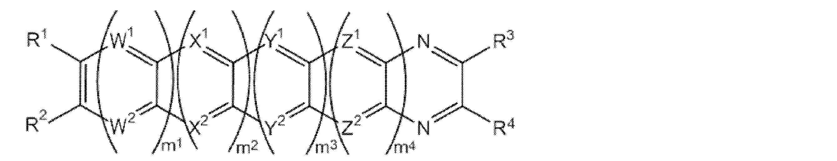
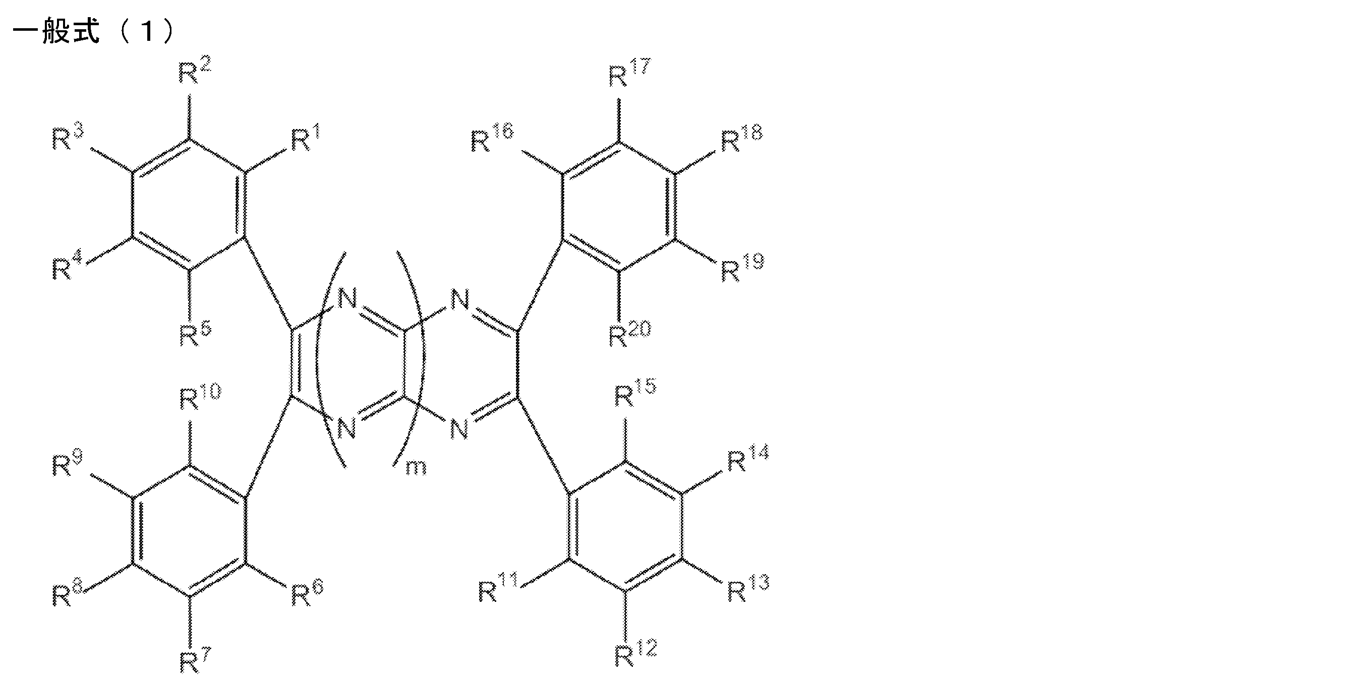
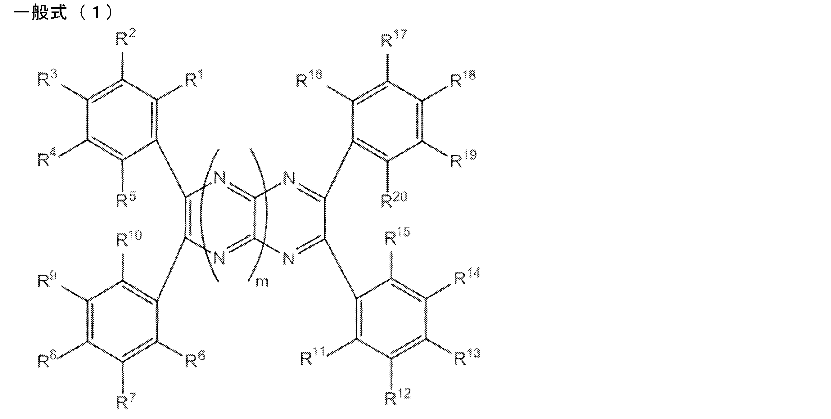
- a light emitting material comprising a compound represented by the following general formula (1).
- R 1 to R 5 each independently represents a hydrogen atom or a substituent having a Hammett's ⁇ p value of 0 or more.
- R 6 to R 20 each independently represents a hydrogen atom or a substituent, and at least one of R 6 to R 20 is a substituted or unsubstituted N, N-diarylamino group.
- m represents 1 or 2.
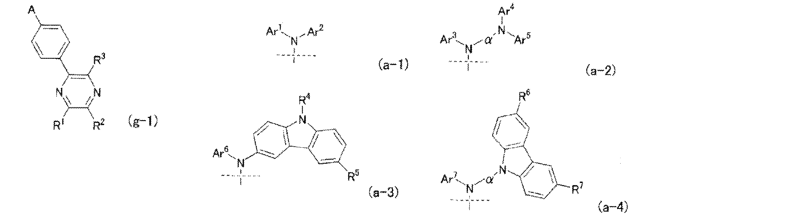
- the groups represented by Ar 1 and Ar 2 may be the same or different. . ]
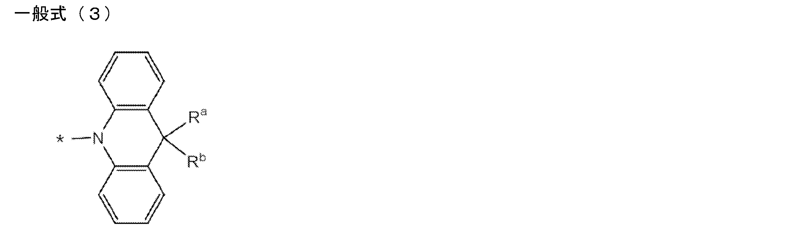
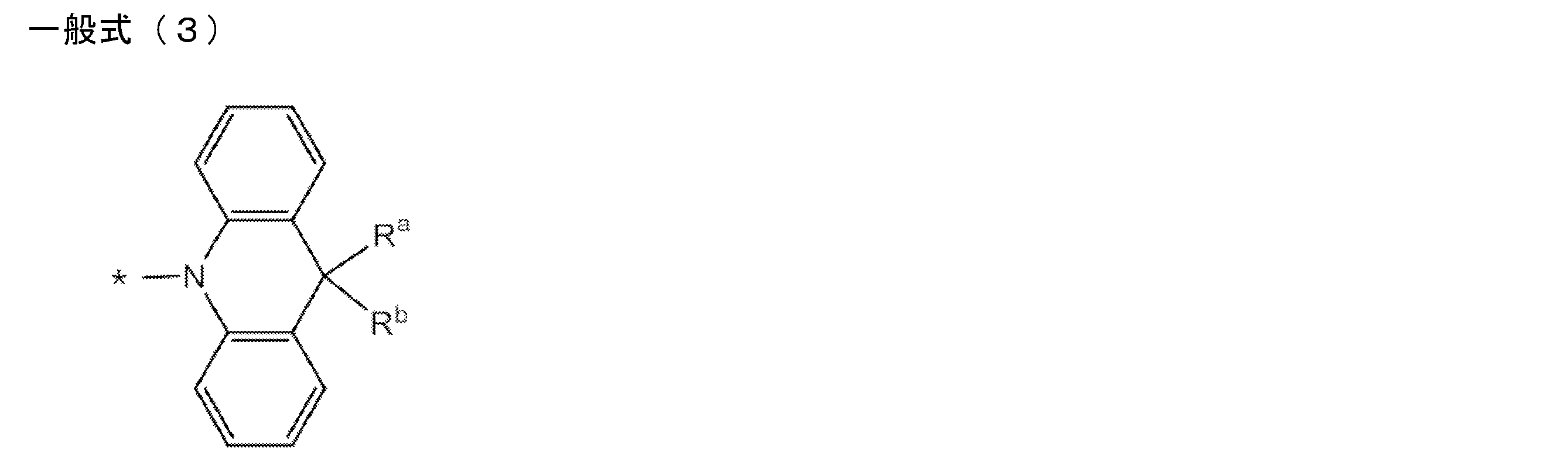
- R a and R b are each independently a hydrogen atom, a substituted or unsubstituted alkyl group having 1 to 5 carbon atoms, or a substituted or unsubstituted aromatic group having 6 to 10 carbon atoms. Represents. * Indicates a binding site.
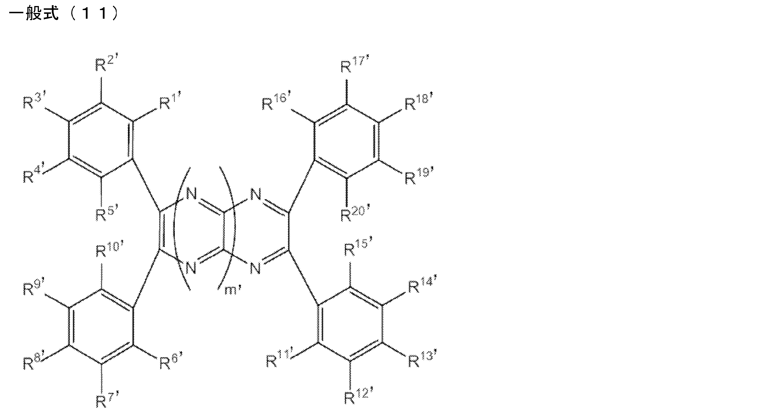
- R 1 ′ to R 5 ′ each independently represents a hydrogen atom or a substituent having a Hammett's ⁇ p value of 0 or more.
- R 6 ′ to R 20 ′ each independently represents a hydrogen atom or a substituent, and at least one of R 6 ′ to R 20 ′ is a substituted or unsubstituted N, N-diarylamino group.
- m ′ represents 1 or 2.
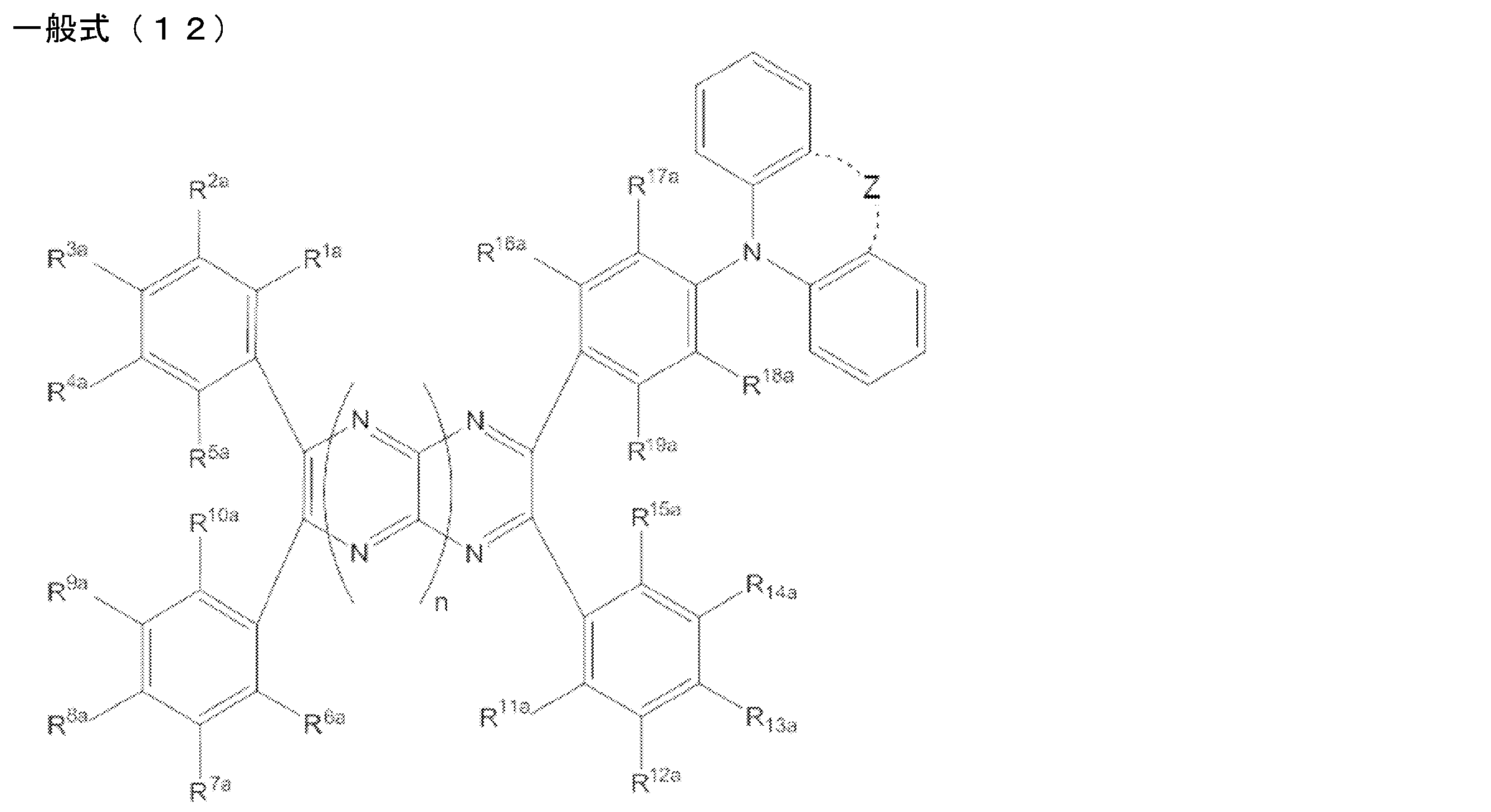
- the compound according to [8], wherein the compound represented by the general formula (11) is represented by the following general formula (12).
- R 1a to R 5a and R 16a to R 19a each independently represent a hydrogen atom or a substituent having a Hammett's ⁇ p value of 0 or more.
- R 6a to R 15a each independently represents a hydrogen atom, a substituent having a Hammett's ⁇ p value of 0 or more, or a substituted or unsubstituted N, N-diarylamino group.
- n represents 1 or 2.
- Z represents a linking group comprising a carbon chain for forming a 6-membered ring or a 7-membered ring, or an oxygen atom for forming a 6-membered ring.
- R 1a to R 5a are each independently a hydrogen atom or a fluorine atom.
- An organic light emitting device comprising a light emitting layer containing the light emitting material according to any one of [1] to [7] on a substrate.
- the organic light-emitting device according to [11] which emits delayed fluorescence.
- Example 2 is an emission spectrum of an organic electroluminescence device of Example Compound (2) in Example 4.
- 6 is a graph showing voltage-current density-luminance characteristics of an organic electroluminescence device of Example Compound (2) of Example 4.
- 6 is a graph showing the current density-current efficiency-power efficiency characteristics of an organic electroluminescent element of Example Compound (2) of Example 4.
- 6 is a graph showing the current density-external quantum efficiency characteristics of an organic electroluminescence device of Example Compound (2) of Example 4.
- the luminescent material of the present invention is characterized by comprising a compound represented by the following general formula (1).
- R 6 to R 20 each independently represents a hydrogen atom or a substituent, and at least one of R 6 to R 20 is a substituted or unsubstituted N, N-diarylamino group.
- a substituted or unsubstituted (N, N-diarylamino group may be any number as long as it is at least one of R 6 to R 20 , but R 6 to R 10 , R 11 to R
- the upper limit of the number of substituted or unsubstituted (N, N-diarylamino groups in each of 15 and R 16 to R 20 is preferably 2, and more preferably 1.
- the substituted or unsubstituted N, N-diarylamino group is not particularly limited, but is one to three of R 7 to R 9 , R 12 to R 14 , and R 17 to R 19. More preferably, it is 1 to 3 of R 7 , R 8 , R 12 , R 13 , R 17 and R 18 , and 1 to 3 of R 8 , R 13 and R 18 It is more preferable that it is at least one of R 13 and R 18 .
- Ar 1 and Ar 2 each independently represents a substituted or unsubstituted aromatic group having 6 to 10 carbon atoms.
- the aromatic group here may be a single ring or a fused ring.
- a phenyl group and a naphthyl group can be mentioned as preferable examples, and a phenyl group is more preferable.
- Specific examples include a phenyl group, a 1-naphthyl group, and a 2-naphthyl group.
- Ar 1 and Ar 2 may be the same or different.
- Ar 1 and Ar 2 may be linked to each other to form a cyclic structure.
- Ar 1 and Ar 2 When linked together to form a cyclic structure, Ar 1 and Ar 2 may be linked directly or indirectly to form a ring. That is, the aromatic group constituting Ar 1 and the aromatic group constituting Ar 2 may be connected to each other by a single bond or may be connected by a linking group.
- the number of linking atoms in the linking group is preferably 1 to 3, more preferably 1 or 2.
- an unsaturated bond may or may not exist between the connecting atoms, but it is preferable that an unsaturated bond exists.
- a linking group represented by the following formula (4) can be mentioned as a preferred example.
- R 21 and R 22 each independently represent a hydrogen atom or a substituent, and R 21 and R 22 may be bonded to each other to form a cyclic structure.
- the cyclic structure include aryl rings such as a benzene ring and a naphthalene ring, heteroaryl rings such as a pyridine ring and a pyrazine ring, and unsaturated aliphatic rings such as a cyclopentadiene ring and a cyclohexene ring.
- N, N-diphenylamino group, N-phenyl-N- (1-naphthyl) amino group, carbazol-9-yl group, and 5H-dibenzo [b, f] azepin-5-yl group are preferable.
- the N, N-diarylamino group exemplified here may be substituted.
- the N, N-diarylamino group represented by the general formula (2) is also preferably a group represented by the following general formula (3).
- R a and R b each independently represent a hydrogen atom, a substituted or unsubstituted alkyl group having 1 to 5 carbon atoms, or a substituted or unsubstituted aromatic group having 6 to 10 carbon atoms.
- the alkyl group that R a and R b can take is not particularly limited as long as it has 1 to 5 carbon atoms, but is preferably a methyl group.
- R a and R b may be the same or different from each other. Further, when the group represented by the general formula (3) is a plurality present in the compounds represented by the general formula (1), and if their R a may be the being the same or different, and , and how their R b may be the being the same or different.
- Substituents of substituted aromatic groups that Ar 1 and Ar 2 in formula (2) can adopt Substituents of substituted alkyl groups and substituted aromatic groups that R a and R b in formula (3) can adopt, and general formulas
- substituents of R 21 and R 22 in (4) can take include, for example, a hydroxy group, a halogen atom, a cyano group, an alkyl group having 1 to 20 carbon atoms, an alkoxy group having 1 to 20 carbon atoms, and a 6 to 40 carbon atom group.
- Substituted or unsubstituted aryloxy group alkylthio group having 1 to 20 carbon atoms, alkyl-substituted amino group having 1 to 20 carbon atoms, acyl group having 2 to 20 carbon atoms, heteroaryl group having 3 to 40 carbon atoms, carbon number A diarylamino group having 12 to 40 carbon atoms, a substituted or unsubstituted carbazolyl group having 12 to 40 carbon atoms, an alkenyl group having 2 to 10 carbon atoms, an alkynyl group having 2 to 10 carbon atoms, and an alkoxycarbon group having 2 to 10 carbon atoms Group, alkylsulfonyl group having 1 to 10 carbon atoms, haloalkyl group having 1 to 10 carbon atoms, amide group, alkylamide group having 2 to 10 carbon atoms, trialkylsilyl group having 3 to 20 carbon atoms, 4 to 20 carbon atoms And a trialkylsilylal
- substituents are a halogen atom, a cyano group, a substituted or unsubstituted alkyl group having 1 to 20 carbon atoms, an alkoxy group having 1 to 20 carbon atoms, a substituted or unsubstituted aryloxy group having 6 to 40 carbon atoms, A substituted or unsubstituted heteroaryl group having 3 to 40 carbon atoms, a substituted or unsubstituted diarylamino group having 12 to 40 carbon atoms, and a substituted or unsubstituted carbazolyl group having 12 to 40 carbon atoms.
- substituents are substituted or unsubstituted alkyl groups having 1 to 10 carbon atoms, substituted or unsubstituted aryloxy groups having 6 to 40 carbon atoms, and substituted or unsubstituted diarylamino groups having 12 to 40 carbon atoms. is there.
- the alkyl group in the present specification may be linear, branched or cyclic, and more preferably has 1 to 6 carbon atoms. Specific examples thereof include a methyl group, an ethyl group, a propyl group, and butyl. Group, t-butyl group, pentyl group, hexyl group and isopropyl group.
- the alkoxy group may be linear, branched or cyclic, and more preferably has 1 to 6 carbon atoms, and specific examples include methoxy group, ethoxy group, propoxy group, butoxy group, t-butoxy group. A group, a pentyloxy group, a hexyloxy group, and an isopropyloxy group.
- the two alkyl groups of the dialkylamino group may be the same or different from each other, but are preferably the same.
- the two alkyl groups of the dialkylamino group may each independently be linear, branched or cyclic, and more preferably have 1 to 6 carbon atoms. Specific examples include a methyl group, an ethyl group, Examples thereof include a propyl group, a butyl group, a pentyl group, a hexyl group, and an isopropyl group.
- the heteroaryl group may be composed of only a single ring or may include a fused ring.
- heteroaryl groups may be a group bonded through a hetero atom or a group bonded through a carbon atom constituting a heteroaryl ring.
- the molecular weight of the compound represented by the general formula (1) is, for example, 1500 or less when the organic layer containing the compound represented by the general formula (1) is intended to be formed by vapor deposition. Preferably, it is preferably 1200 or less, more preferably 1000 or less, and even more preferably 800 or less.
- the lower limit of the molecular weight is the molecular weight of the compound having the smallest molecular weight represented by the general formula (1).
- the compound represented by the general formula (1) may be formed by a coating method regardless of the molecular weight. If a coating method is used, a film can be formed even with a compound having a relatively large molecular weight.
- a compound containing a plurality of structures represented by the general formula (1) in the molecule for the light emitting layer of the organic light emitting device.
- a polymer obtained by polymerizing a polymerizable monomer having a structure represented by the general formula (1) for a light emitting layer of an organic light emitting device Specifically, by preparing a monomer having a polymerizable functional group in any of R 1 to R 20 in the general formula (1) and polymerizing it alone or copolymerizing with other monomers, It is considered that a polymer having a repeating unit is obtained and the polymer is used for a light emitting layer of an organic light emitting device.
- dimers and trimers are obtained by reacting compounds having a structure represented by the general formula (1) and used in the light emitting layer of the organic light emitting device.
- any one of R 1 ⁇ R 20 in the general formula (1) is the following general formula (21) or (22) The thing which is a structure represented can be mentioned.
- the polymer containing the structure represented by the general formula (1) in the molecule may be a polymer composed only of repeating units having the structure represented by the general formula (1), or other structures may be used. It may be a polymer containing repeating units.
- the repeating unit having a structure represented by the general formula (1) contained in the polymer may be a single type or two or more types. Examples of the repeating unit not having the structure represented by the general formula (1) include those derived from monomers used in ordinary copolymerization. Examples thereof include a repeating unit derived from a monomer having an ethylenically unsaturated bond such as ethylene and styrene.
- R 1a to R 5a and R 16a to R 19a see the explanation and preferred examples of the substituents that R 1 to R 5 of formula (1) can take.
- the substituents represented by R 1a to R 5a are preferably fluorine atoms.
- the explanation and preferred range of the N, N-diarylamino group that R 6a to R 15a can take the explanation and preferred range of the N, N-diarylamino group that R 6 to R 20 of the general formula (1) can take are as follows. You can refer to it. n is 1 or 2, and is preferably 1. When Z is a carbon chain, the carbon number of the carbon chain is 1 or 2.
- R 1 ′ to R 17 ′ , R 19 ′ and R 20 ′ in the scheme are groups having the same meanings as those in the general formula (11).
- R a and R b are the same groups as those in the general formula (3).
- X represents a halogen atom. Examples of the halogen atom include a fluorine atom, a chlorine atom, a bromine atom, and an iodine atom, and a fluorine atom, a chlorine atom, and a bromine atom are preferable.
- reaction conditions and procedures of each step known reaction conditions and procedures adopted in similar synthesis reactions can be appropriately selected and adopted.
- the compound represented by the general formula (1) of the present invention is useful as a light emitting material of an organic light emitting device. For this reason, the compound represented by General formula (1) of this invention can be effectively used as a luminescent material for the light emitting layer of an organic light emitting element.
- the compound represented by the general formula (1) includes a delayed fluorescent material (delayed phosphor) that emits delayed fluorescence. That is, the present invention relates to a delayed phosphor having a structure represented by the general formula (1), an invention using a compound represented by the general formula (1) as a delayed phosphor, and a general formula (1).
- An invention of a method for emitting delayed fluorescence using the represented compound is also provided.
- An organic light emitting device using such a compound as a light emitting material emits delayed fluorescence and has a feature of high luminous efficiency. The principle will be described below by taking an organic electroluminescence element as an example.
- the organic electroluminescence element carriers are injected into the light emitting material from both positive and negative electrodes to generate an excited light emitting material and emit light.
- 25% of the generated excitons are excited to the excited singlet state, and the remaining 75% are excited to the excited triplet state. Therefore, the use efficiency of energy is higher when phosphorescence, which is light emission from an excited triplet state, is used.
- the excited triplet state has a long lifetime, energy saturation occurs due to saturation of the excited state and interaction with excitons in the excited triplet state, and in general, the quantum yield of phosphorescence is often not high.
- the light is emitted from the excited singlet, the light is emitted at the same wavelength as the fluorescence. Since the fluorescence becomes longer than the fluorescence and phosphorescence, it is observed as fluorescence delayed from these. This can be defined as delayed fluorescence. If such a heat-activated exciton transfer mechanism is used, the ratio of the compound in an excited singlet state, which normally generated only 25%, is increased to 25% or more by absorbing thermal energy after carrier injection. It can be raised. If a compound that emits strong fluorescence and delayed fluorescence even at a low temperature of less than 100 ° C is used, the heat of the device will sufficiently cause intersystem crossing from the excited triplet state to the excited singlet state and emit delayed fluorescence. Efficiency can be improved dramatically.
- the compound represented by the general formula (1) of the present invention as a light-emitting material of a light-emitting layer, excellent organic light-emitting devices such as an organic photoluminescence device (organic PL device) and an organic electroluminescence device (organic EL device) Can be provided.
- the compound represented by the general formula (1) of the present invention may have a function of assisting light emission of another light emitting material included in the light emitting layer as a so-called assist dopant. That is, the compound represented by the general formula (1) of the present invention contained in the light emitting layer includes the lowest excitation singlet energy level of the host material contained in the light emitting layer and the lowest excitation of other light emitting materials contained in the light emitting layer.
- the hole transport layer may be a hole injection / transport layer having a hole injection function
- the electron transport layer may be an electron injection / transport layer having an electron injection function.
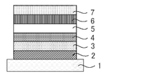
- FIG. 1 A specific example of the structure of an organic electroluminescence element is shown in FIG.
- 1 is a substrate
- 2 is an anode
- 3 is a hole injection layer
- 4 is a hole transport layer
- 5 is a light emitting layer
- 6 is an electron transport layer
- 7 is a cathode.
- each member and each layer of an organic electroluminescent element are demonstrated.
- substrate and a light emitting layer corresponds also to the board
- the organic electroluminescence device of the present invention is preferably supported on a substrate.
- the substrate is not particularly limited and may be any substrate conventionally used for organic electroluminescence elements.
- a substrate made of glass, transparent plastic, quartz, silicon, or the like can be used.
- an electrode material made of a metal, an alloy, an electrically conductive compound, or a mixture thereof having a high work function (4 eV or more) is preferably used.
- electrode materials include metals such as Au, and conductive transparent materials such as CuI, indium tin oxide (ITO), SnO 2 , and ZnO.
- conductive transparent materials such as CuI, indium tin oxide (ITO), SnO 2 , and ZnO.
- an amorphous material such as IDIXO (In 2 O 3 —ZnO) that can form a transparent conductive film may be used.
- cathode a material having a low work function (4 eV or less) metal (referred to as an electron injecting metal), an alloy, an electrically conductive compound, and a mixture thereof as an electrode material is used.
- electrode materials include sodium, sodium-potassium alloy, magnesium, lithium, magnesium / copper mixture, magnesium / silver mixture, magnesium / aluminum mixture, magnesium / indium mixture, aluminum / aluminum oxide (Al 2 O 3 ) Mixtures, indium, lithium / aluminum mixtures, rare earth metals and the like.
- the sheet resistance as the cathode is preferably several hundred ⁇ / ⁇ or less, and the film thickness is usually selected in the range of 10 nm to 5 ⁇ m, preferably 50 to 200 nm.
- the emission luminance is advantageously improved.
- a transparent or semi-transparent cathode can be produced. By applying this, an element in which both the anode and the cathode are transparent is used. Can be produced.
- the light emitting layer is a layer that emits light after excitons are generated by recombination of holes and electrons injected from each of the anode and the cathode, and the light emitting material may be used alone for the light emitting layer. , Preferably including a luminescent material and a host material.
- a luminescent material the 1 type (s) or 2 or more types chosen from the compound group of this invention represented by General formula (1) can be used.
- a host material in addition to the light emitting material in the light emitting layer.
- the host material an organic compound having at least one of excited singlet energy and excited triplet energy higher than that of the light emitting material of the present invention can be used.
- singlet excitons and triplet excitons generated in the light emitting material of the present invention can be confined in the molecules of the light emitting material of the present invention, and the light emission efficiency can be sufficiently extracted.
- high luminous efficiency can be obtained, so that host materials that can achieve high luminous efficiency are particularly limited. And can be used in the present invention.
- the organic light emitting device or organic electroluminescent device of the present invention light emission is generated from the light emitting material of the present invention contained in the light emitting layer. This emission includes both fluorescence and delayed fluorescence. However, light emission from the host material may be partly or partly emitted.
- the amount of the compound of the present invention, which is a light emitting material is preferably 0.1% by weight or more, more preferably 1% by weight or more, and 50% or more. It is preferably no greater than wt%, more preferably no greater than 20 wt%, and even more preferably no greater than 10 wt%.
- the host material in the light-emitting layer is preferably an organic compound that has a hole transporting ability and an electron transporting ability, prevents the emission of longer wavelengths, and has a high glass transition temperature.
- the injection layer is a layer provided between the electrode and the organic layer for lowering the driving voltage and improving the luminance of light emission.
- the injection layer can be provided as necessary.
- the blocking layer is a layer that can prevent diffusion of charges (electrons or holes) and / or excitons existing in the light emitting layer to the outside of the light emitting layer.
- the electron blocking layer can be disposed between the light emitting layer and the hole transport layer and blocks electrons from passing through the light emitting layer toward the hole transport layer.
- a hole blocking layer can be disposed between the light emitting layer and the electron transporting layer to prevent holes from passing through the light emitting layer toward the electron transporting layer.
- the blocking layer can also be used to block excitons from diffusing outside the light emitting layer. That is, each of the electron blocking layer and the hole blocking layer can also function as an exciton blocking layer.
- the term “electron blocking layer” or “exciton blocking layer” as used herein is used in the sense of including a layer having the functions of an electron blocking layer and an exciton blocking layer in one layer.
- the hole blocking layer has a function of an electron transport layer in a broad sense.
- the hole blocking layer has a role of blocking holes from reaching the electron transport layer while transporting electrons, thereby improving the recombination probability of electrons and holes in the light emitting layer.
- the material for the hole blocking layer the material for the electron transport layer described later can be used as necessary.
- the layer when the exciton blocking layer is provided on the anode side, the layer can be inserted adjacent to the light emitting layer between the hole transport layer and the light emitting layer, and when inserted on the cathode side, the light emitting layer and the cathode Between the luminescent layer and the light-emitting layer.
- a hole injection layer, an electron blocking layer, or the like can be provided between the anode and the exciton blocking layer adjacent to the anode side of the light emitting layer, and the excitation adjacent to the cathode and the cathode side of the light emitting layer can be provided.
- an electron injection layer, an electron transport layer, a hole blocking layer, and the like can be provided.
- the blocking layer is disposed, at least one of the excited singlet energy and the excited triplet energy of the material used as the blocking layer is preferably higher than the excited singlet energy and the excited triplet energy of the light emitting material.
- the hole transport layer is made of a hole transport material having a function of transporting holes, and the hole transport layer can be provided as a single layer or a plurality of layers.
- the hole transport material has any one of hole injection or transport and electron barrier properties, and may be either organic or inorganic.
- hole transport materials that can be used include, for example, triazole derivatives, oxadiazole derivatives, imidazole derivatives, carbazole derivatives, indolocarbazole derivatives, polyarylalkane derivatives, pyrazoline derivatives and pyrazolone derivatives, phenylenediamine derivatives, arylamine derivatives, Examples include amino-substituted chalcone derivatives, oxazole derivatives, styrylanthracene derivatives, fluorenone derivatives, hydrazone derivatives, stilbene derivatives, silazane derivatives, aniline copolymers, and conductive polymer oligomers, particularly thiophene oligomers.
- An aromatic tertiary amine compound and an styrylamine compound are preferably used, and an aromatic tertiary amine compound is more preferably used.
- the electron transport layer is made of a material having a function of transporting electrons, and the electron transport layer can be provided as a single layer or a plurality of layers.
- the electron transport material (which may also serve as a hole blocking material) may have a function of transmitting electrons injected from the cathode to the light emitting layer.
- Examples of the electron transport layer that can be used include nitro-substituted fluorene derivatives, diphenylquinone derivatives, thiopyran dioxide oxide derivatives, carbodiimides, fluorenylidenemethane derivatives, anthraquinodimethane and anthrone derivatives, oxadiazole derivatives, and the like.
- the compound represented by the general formula (1) may be used not only for the light emitting layer but also for layers other than the light emitting layer.
- the compound represented by General formula (1) used for a light emitting layer and the compound represented by General formula (1) used for layers other than a light emitting layer may be same or different.
- the compound represented by the general formula (1) may be used for the injection layer, blocking layer, hole blocking layer, electron blocking layer, exciton blocking layer, hole transporting layer, electron transporting layer, and the like. .
- the method for forming these layers is not particularly limited, and the layer may be formed by either a dry process or a wet process.
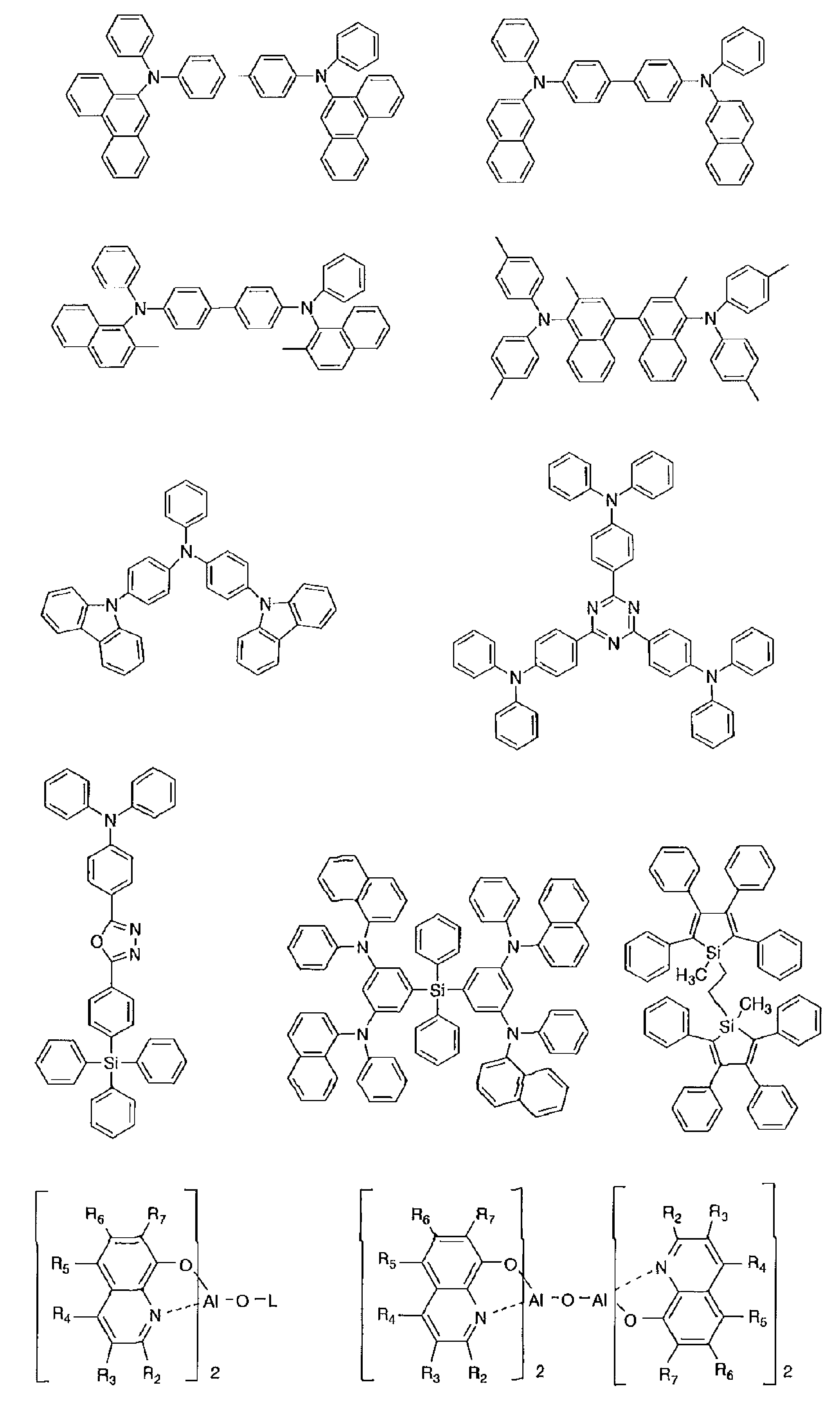
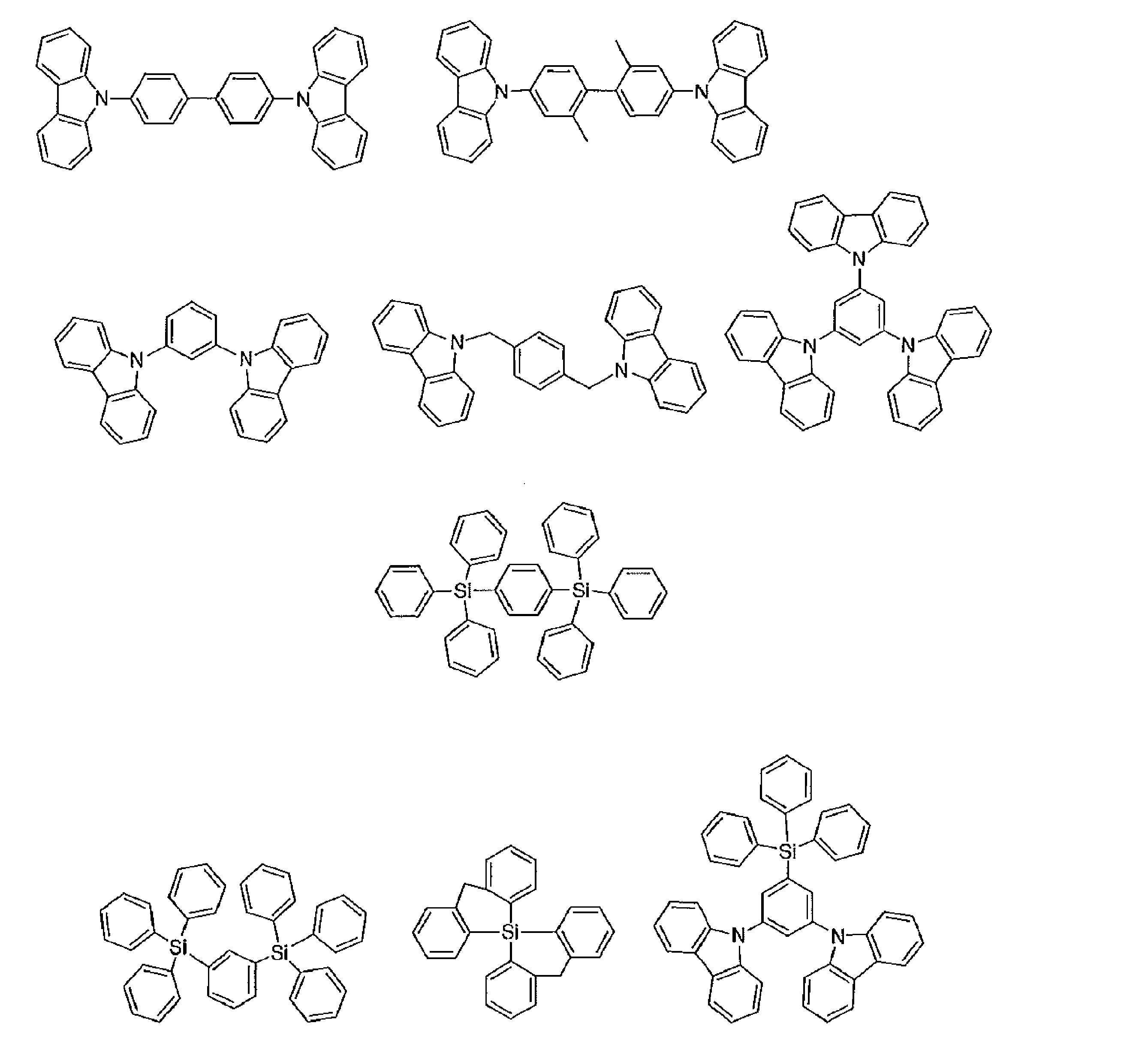
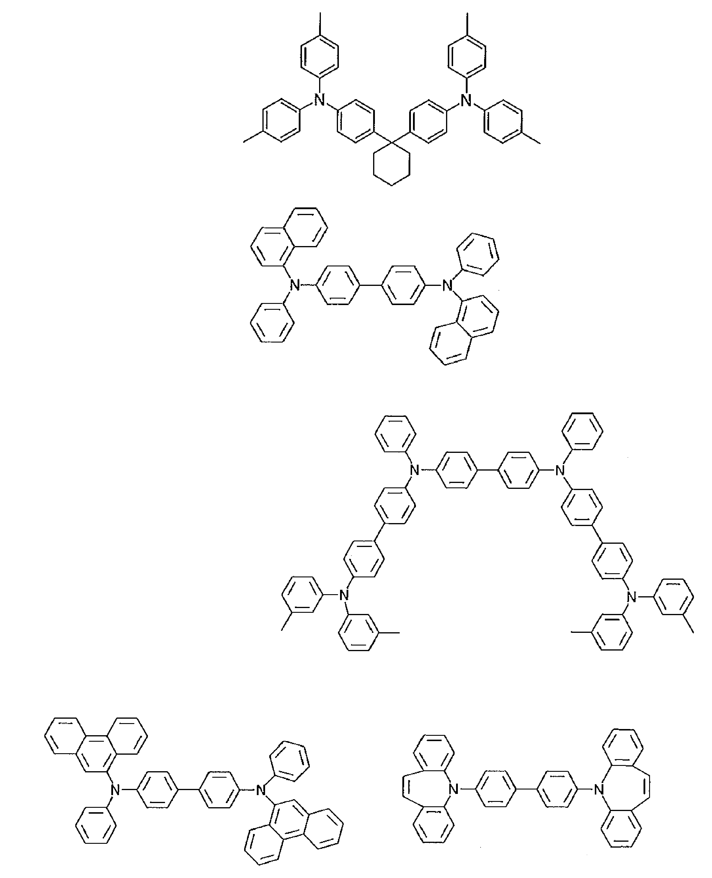
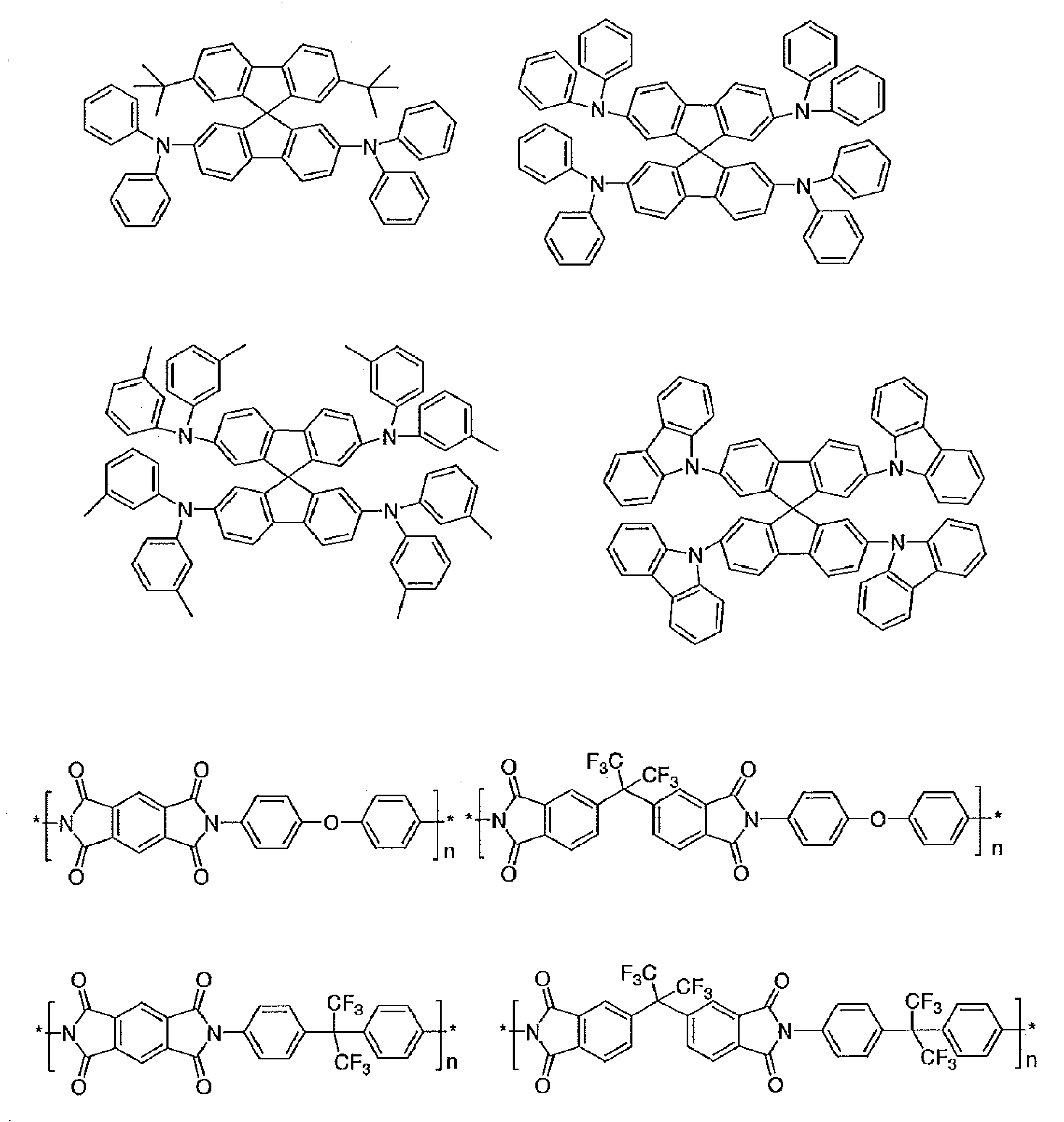
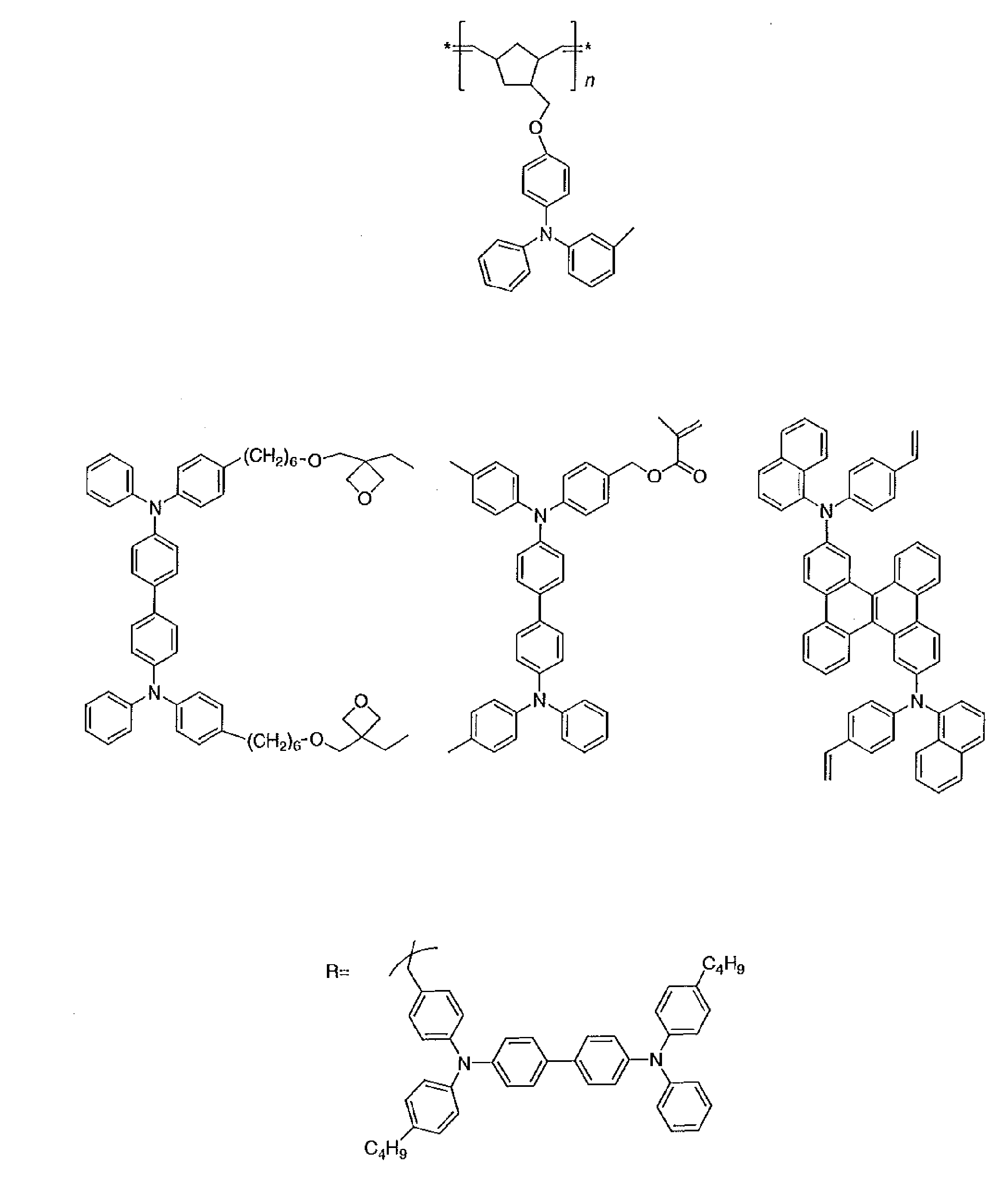
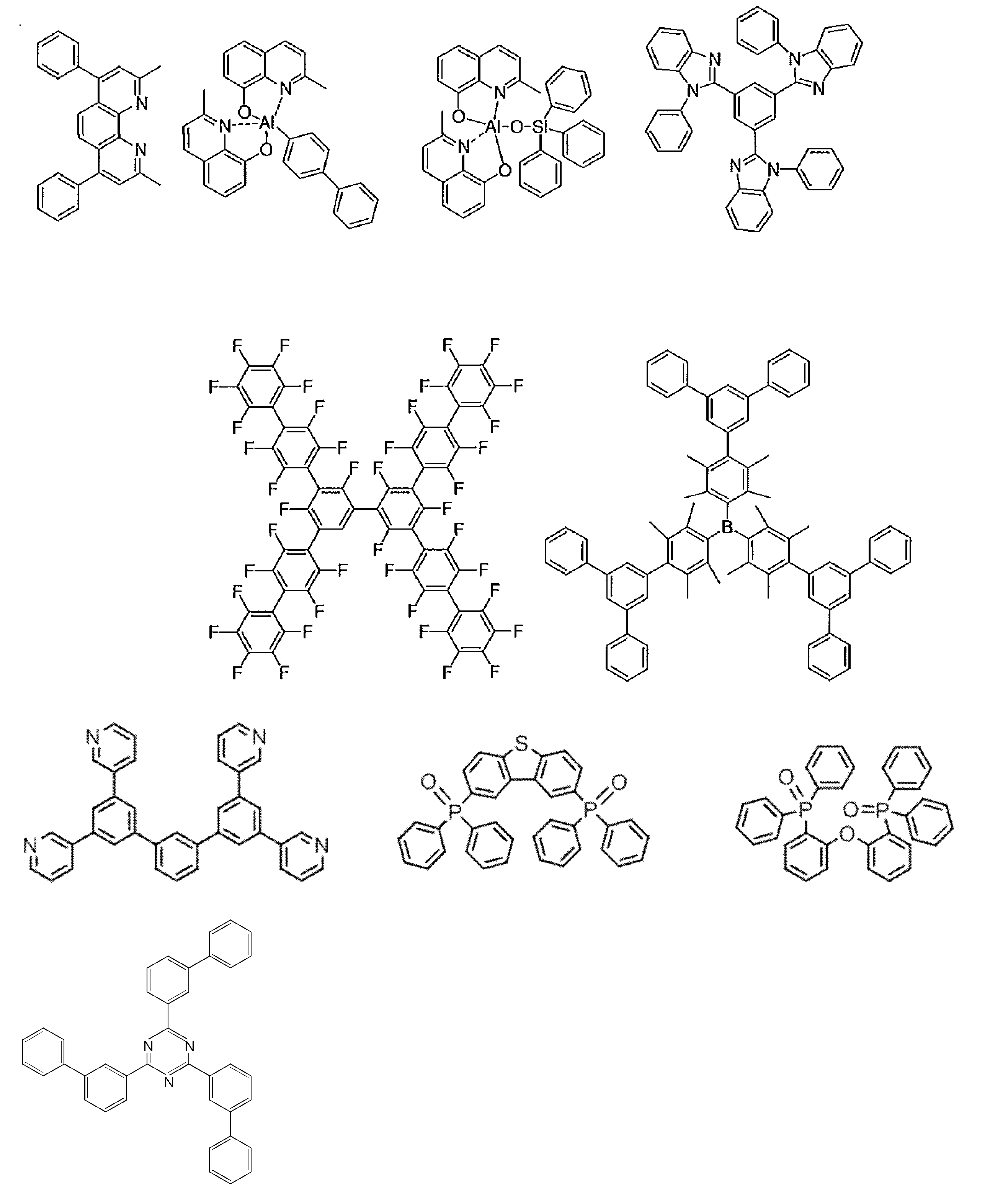
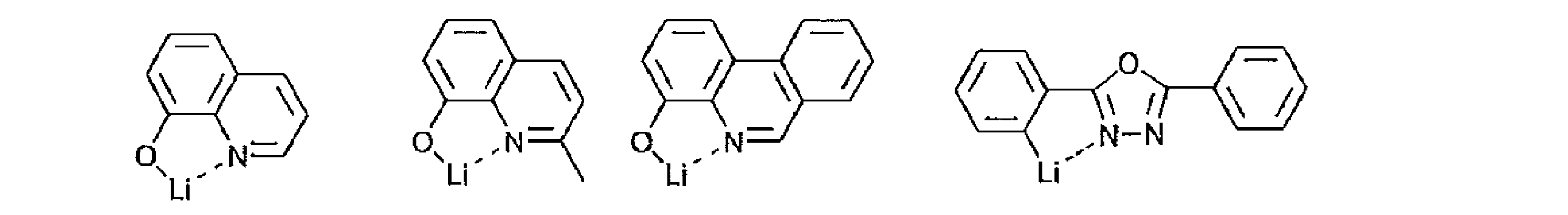
- the preferable material which can be used for an organic electroluminescent element is illustrated concretely.
- the material that can be used in the present invention is not limited to the following exemplary compounds. Moreover, even if it is a compound illustrated as a material which has a specific function, it can also be diverted as a material which has another function.
- R and R 2 to R 7 each independently represent a hydrogen atom or a substituent.
- n represents an integer of 3 to 5.
- the organic electroluminescence device produced by the above-described method emits light by applying an electric field between the anode and the cathode of the obtained device. At this time, if the light is emitted by excited singlet energy, light having a wavelength corresponding to the energy level is confirmed as fluorescence emission and delayed fluorescence emission. In addition, in the case of light emission by excited triplet energy, a wavelength corresponding to the energy level is confirmed as phosphorescence. Since normal fluorescence has a shorter fluorescence lifetime than delayed fluorescence, the emission lifetime can be distinguished from fluorescence and delayed fluorescence.
- the excited triplet energy is unstable and is converted into heat and the like, and the lifetime is short and it is immediately deactivated.
- the excited triplet energy of a normal organic compound it can be measured by observing light emission under extremely low temperature conditions.
- the organic electroluminescence element of the present invention can be applied to any of a single element, an element having a structure arranged in an array, and a structure in which an anode and a cathode are arranged in an XY matrix. According to the present invention, an organic light emitting device with greatly improved light emission efficiency can be obtained by containing the compound represented by the general formula (1) in the light emitting layer.
- the organic light emitting device such as the organic electroluminescence device of the present invention can be further applied to various uses. For example, it is possible to produce an organic electroluminescence display device using the organic electroluminescence element of the present invention.
- organic electroluminescence device of the present invention can be applied to organic electroluminescence illumination and backlights that are in great demand.
- source meter manufactured by Keithley: 2400 series
- semiconductor parameter analyzer manufactured by Agilent Technologies: E5273A
- optical power meter measuring device manufactured by Newport: 1930C
- optical spectrometer Ocean Optics, USB2000
- spectroradiometer Topcon, SR-3
- streak camera Haamamatsu Photonics C4334
- Singlet energy E S1 A sample having a thickness of 100 nm was prepared on a Si substrate by co-evaporating the measurement target compound and mCBP so that the measurement target compound had a concentration of 6% by weight. The fluorescence spectrum of this sample was measured at room temperature (300K).
- a fluorescence spectrum having a luminescence intensity on the vertical axis and a wavelength on the horizontal axis was obtained.
- the vertical axis represents light emission and the horizontal axis represents wavelength.
- a tangent line was drawn with respect to the short-wave rise of the emission spectrum, and the wavelength value ⁇ edge [nm] at the intersection of the tangent line and the horizontal axis was obtained.
- a value obtained by converting this wavelength value into an energy value by the following conversion formula was defined as E S1 .
- E S1 [eV] 1239.85 / ⁇ edge
- a nitrogen laser Lasertechnik Berlin, MNL200
- a streak camera Hamamatsu Photonics, C4334
- E T1 Triplet energy
- tangents at each point on the curve are considered toward the long wavelength side.
- the slope of this tangent line increases as the curve rises (that is, as the vertical axis increases).
- the tangent drawn at the point where the value of the slope takes the maximum value was taken as the tangent to the rising edge of the phosphorescence spectrum on the short wavelength side.
- the maximum point having a peak intensity of 10% or less of the maximum peak intensity of the spectrum is not included in the above-mentioned maximum value on the shortest wavelength side, and has the maximum slope value closest to the maximum value on the shortest wavelength side.
- the tangent drawn at the point where the value was taken was taken as the tangent to the rising edge of the phosphorescence spectrum on the short wavelength side.
- WO2012 / 039561 and tris (dibenzylideneacetone) di Palladium (0) (36 mg, 0.039 mmol), sodium tert-butoxide (41 mg, 0.43 mmol), toluene 20 ml, tri (tert-butyl) phosphine (10 mg, 0.050 mmol) were charged into a 100 ml three-necked flask and stirred. While degassing and nitrogen substitution were quickly repeated three times. The mixture was stirred at reflux for 8 hours under a nitrogen stream. After the reaction, water was added to the reaction solution allowed to cool to room temperature, extracted with dichloromethane, and washed with saturated brine.
- Example 1 Preparation and Evaluation of Solution of Illustrative Compound (1)
- a toluene solution (concentration 10 ⁇ 5 M) of Illustrative Compound (1) synthesized in Synthesis Example 1 was prepared.
- the photoluminescence quantum efficiency was 12.5% with the toluene solution without bubbling, and 33.4% with the toluene solution with nitrogen bubbling.
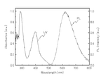
- the result of having measured the emission spectrum and ultraviolet absorption spectrum by 400 nm excitation light about this toluene solution is shown in FIG.
- the maximum emission wavelength ⁇ max was 651 nm.
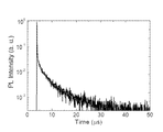
- the transient decay curve shows the result of measuring the luminescence lifetime obtained by measuring the process in which the emission intensity is deactivated by applying excitation light to the compound.
- the light emission intensity decays in a single exponential manner. This means that if the vertical axis of the graph is semi-log, it will decay linearly.
- the transient decay curve of the exemplary compound (1) shown in FIG. 3 such a linear component (fluorescence) is observed in the early stage of observation, but a component deviating from linearity appears after several ⁇ sec.
- the exemplary compound (1) is a light emitter containing a delay component in addition to the fluorescent component.
- the emission lifetime was 0.37 ⁇ s for the toluene solution without bubbling, and 36.1 ⁇ s for the toluene solution with nitrogen bubbling.
- the energy difference ⁇ E st between the excited singlet state and the excited triplet state of this toluene solution was 0.002 eV, and the f value as a frequency factor for the S 0 ⁇ S 1 transition was 0.0002.
- the ⁇ E st value was used as a measure of the probability of thermal activation, and it was considered that the smaller the value, the more likely the thermal activation delayed fluorescence occurs.
- the f value is the ease of the transition from S 0 (ground state) to S 1 (excited singlet state). In this calculation, the f value is used as a measure of the ease of light emission (fluorescence intensity). It was considered that the larger this value, the stronger the fluorescence.
- Example 2 Preparation and Evaluation of Solution of Exemplary Compound (2)
- the photoluminescence quantum efficiency by 440 nm excitation light was measured about this toluene solution, the photoluminescence quantum efficiency was 12.0% with the toluene solution without bubbling, and 32.4% with the toluene solution with nitrogen bubbling. .
- FIG. 4 the result of having measured the emission spectrum and ultraviolet absorption spectrum by 444 nm excitation light is shown in FIG. 4
- the result of having measured the transient decay curve by 340 nm excitation light is shown in FIG. From FIG.
- the maximum emission wavelength ⁇ max was 621 nm. From FIG. 5, a component having a short emission lifetime (immediate fluorescence component) and a component having a long emission lifetime (delayed fluorescence component) can be observed, and the emission lifetime of the delayed fluorescence component is 0.40 ⁇ s in a toluene solution without bubbling. It was 23.5 ⁇ s with a toluene solution subjected to nitrogen bubbling. Further, the energy difference ⁇ E st between the excited singlet state and the excited triplet state of this toluene solution was 0.002 eV, and the f value was 0.
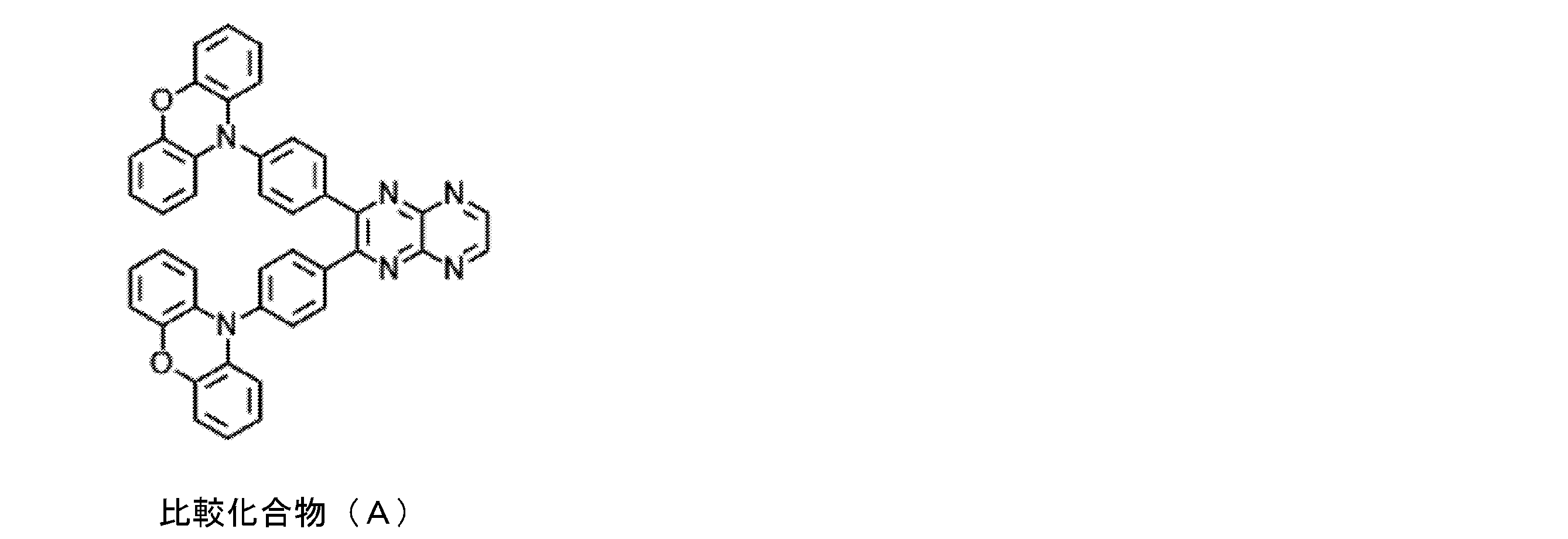
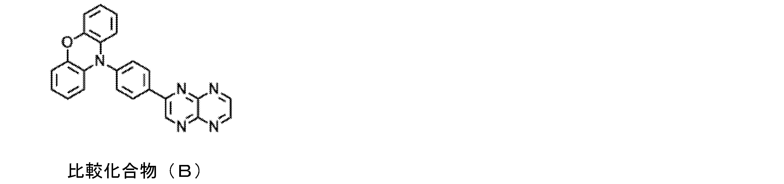
- Comparative Example 1 Preparation and Evaluation of Solution of Comparative Compound (A) A toluene solution (concentration 10 ⁇ 5 M) of comparative compound (A) was prepared. When the characteristics of this toluene solution were evaluated, the photoluminescence quantum efficiency by 320 nm excitation light was 1.2% in the toluene solution without bubbling, and 2.3% in the toluene solution with nitrogen bubbling, and the maximum emission wavelength. was 706 nm. The energy difference ⁇ E st between the excited singlet state and the excited triplet state was 0.047 eV, and the f value was 0.031. The toluene solution of this comparative compound (A) was weak in luminescence, and delayed fluorescence could not be confirmed.
- Comparative Example 2 Preparation and Evaluation of Solution of Comparative Compound (B)
- a toluene solution (concentration 10 ⁇ 5 M) of comparative compound (B) was prepared.
- the photoluminescence quantum efficiency by 360 nm excitation light was 1.1% in the toluene solution without bubbling and 2.3% in the toluene solution with nitrogen bubbling, and the maximum emission wavelength. was 697 nm.
- the energy difference ⁇ E st between the excited singlet state and the excited triplet state was 0.006 eV, and f was 0.041.
- the toluene solution of this comparative compound (B) was weak in luminescence, and delayed fluorescence could not be confirmed.
- Comparative Example 3 Preparation and Evaluation of Solution of Comparative Compound (C) A toluene solution (concentration 10 ⁇ 5 M) of comparative compound (C) was prepared. When photoluminescence by 360 nm excitation light was observed using this toluene solution, delayed fluorescence could not be clearly confirmed.
- Example 3 Production and evaluation of thin film type organic photoluminescence device of exemplary compound (2) Exemplified compound (2) under the condition of a vacuum degree of 3.0 ⁇ 10 ⁇ 4 Pa or less by vacuum deposition on a silicon substrate. ) And mCBP were vapor-deposited from different vapor deposition sources, and a thin film having a concentration of the exemplary compound (2) of 6.0% by weight was formed to a thickness of 50 nm to obtain a thin-film organic photoluminescence device.
- FIG. 6 shows the results of measuring the emission spectrum and ultraviolet absorption spectrum of the thin-film organic photoluminescence device with 400 nm excitation light
- FIG. 7 shows the results of measuring the transient decay curve in the atmosphere.
- the photoluminescence quantum efficiency was 48.9% in the air, 50.1% in the nitrogen-containing atmosphere, and the emission wavelength was 586 nm. Further, from FIG. 7, three components having different emission lifetimes can be observed, and the emission lifetimes of the respective components were 7.81 ns, 969.0 ns, and 5.73 ⁇ s.
- Example 4 Production and evaluation of organic electroluminescence device using exemplary compound (2) Each thin film was vacuum-deposited on a glass substrate on which an anode made of indium tin oxide (ITO) having a thickness of 100 nm was formed. In this way, the layers were laminated at a vacuum degree of 3.0 ⁇ 10 ⁇ 4 Pa. First, ⁇ -NPD was formed on ITO to a thickness of 35 nm. Next, Exemplified Compound (2) and mCBP were co-evaporated from different vapor deposition sources to form a layer having a thickness of 15 nm as a light emitting layer. At this time, the concentration of the exemplary compound (2) was 6.0% by weight.
- ITO indium tin oxide
- TPBi is formed to a thickness of 65 nm
- further lithium fluoride (LiF) is vacuum-deposited to 0.8 nm
- aluminum (Al) is evaporated to a thickness of 100 nm to form a cathode.
- a luminescence element was obtained.
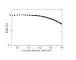
- the organic electroluminescent device was manufactured, the emission spectrum measured in each condition of 1mA / cm 2, 10mA / cm 2, 100mA / cm 2 shown in FIG. 8, a voltage - current density - shows the luminance characteristics in FIG. 9, the current FIG. 10 shows the density-current efficiency-power efficiency characteristics, and FIG. 11 shows the current density-external quantum efficiency characteristics.
- This organic electroluminescence device had a turn-on voltage of 3.2 V, a maximum luminance of 14820 cd / m 2 , a maximum current efficiency of 27.7 cd / A, and a maximum power efficiency of 25.1 lm / W. Further, this organic electroluminescence device achieved a high external quantum yield of 10.5%. Assuming that an ideal organic electroluminescence device balanced using a fluorescent material having a light emission quantum efficiency of 100% is prototyped, if the light extraction efficiency is 20 to 30%, the external quantum efficiency of fluorescence emission is 5%. 7.5%. This value is generally regarded as a theoretical limit value of the external quantum efficiency of an organic electroluminescence device using a fluorescent material. The organic electroluminescence device of the present invention is extremely excellent in that high external quantum efficiency exceeding the theoretical limit value is realized.
- the organic light emitting device of the present invention can realize high luminous efficiency.
- the compound of the present invention is useful as a light emitting material for such an organic light emitting device. For this reason, this invention has high industrial applicability.
Abstract
Description
これに対して、本発明者らがポリアザアセン骨格に(N,N-ジアリールアミノ)アリール基が置換した構造を有する化合物群について種々の検討を始めたところ、ポリアザアセン骨格に(N,N-ジアリールアミノ)アリール基とN,N-ジアリールアミノ基を有しないアリール基が置換した構造を有する化合物群に発光材料として高い有用性があることを初めて見出し、さらに検討を進めることにした。上記のように、ポリアザアセン骨格に(N,N-ジアリールアミノ)アリール基が置換した化合物については、特許文献1において有機発光素子の発光材料として有用であることが記載されている。しかし、同文献では、ポリアザアセン骨格に(N,N-ジアリールアミノ)アリール基とN,N-ジアリールアミノ基を有しないアリール基が置換した化合物については検討がなされていない。一方、特許文献2には、単環のピラジン環に4-(N,N-ジフェニルアミノ)フェニル基と置換基を有しないフェニル基が置換した化合物が記載されている。しかし、同文献には複数のピラジン環が融合したポリアザアセン骨格を有する化合物は記載されていない。このため、ポリアザアセン骨格に(N,N-ジアリールアミノ)アリール基とN,N-ジアリールアミノ基を有しないアリール基が置換した化合物の発光材料としての有用性は全く予測がつかない。

[2] 前記ハメットのσp値が0以上の置換基が、ハロゲン原子、アシルオキシ基、アルコキシカルボニル基、アリールオキシカルボニル基、フェニル基またはシアノ基であることを特徴とする[1]に記載の発光材料。
[3] 前記置換もしくは無置換のN,N-ジアリールアミノ基が下記一般式(2)で表わされる基であることを特徴とする[1]または[2]に記載の発光材料。

[4] 前記Ar1およびAr2は直接もしくは間接に連結して環を形成していることを特徴とする[3]に記載の発光材料。
[5] 前記一般式(2)で表される基が、下記一般式(3)で表されることを特徴とする[4]に記載の発光材料。

[6] 前記一般式(1)において、mが1であることを特徴とする[1]~[5]のいずれか1項に記載の発光材料。
[7] 遅延蛍光を放射することを特徴とする[1]~[6]のいずれか1項に記載の発光材料。
[8] 下記一般式(11)で表わされる化合物。
[9] 一般式(11)で表わされる化合物が、下記一般式(12)で表わされることを特徴とする[8]に記載の化合物。

[10] 前記R1a~R5aが、各々独立に水素原子またはフッ素原子であることを特徴とする[9]に記載の化合物。
[11] [1]~[7]のいずれか1項に記載の発光材料を含む発光層を基板上に有することを特徴とする有機発光素子。
[12] 遅延蛍光を放射することを特徴とする[11]に記載の有機発光素子。
[13] 有機エレクトロルミネッセンス素子であることを特徴とする[11]または[12]に記載の有機発光素子。
本発明の発光材料は、下記一般式(1)で表される化合物からなることを特徴とする。
ハメットのσp値が0以上の置換基として、例えばハロゲン原子、アシルオキシ基、アルコキシカルボニル基、アリールオキシカルボニル基、フェニル基またはシアノ基を挙げることができ、このうちハロゲン原子、シアノ基であることが好ましく、ハロゲン原子であることがより好ましい。R1~R5のうちの置換基の数は特に制限されず、すべてが無置換(すなわち水素原子)であってもよい。また、R1~R5のうちの2つ以上が置換基である場合、複数の置換基は互いに同一であっても異なっていてもよい。
R6~R20は、各々独立に水素原子もしくは置換基を表すが、R6~R20の少なくとも一つは置換もしくは無置換のN,N-ジアリールアミノ基である。置換もしくは無置換の(N,N-ジアリールアミノ基を表すのは、R6~R20のうちの1つ以上であれば幾つであってもよいが、R6~R10、R11~R15、R16~R20のそれぞれにおける置換もしくは無置換の(N,N-ジアリールアミノ基の数の上限は2つであることが好ましく、1つであることがより好ましい。R6~R20のうち置換もしくは無置換のN,N-ジアリールアミノ基を表すのは、特に制限されないが、R7~R9、R12~R14、R17~R19のうちの1~3つであることが好ましく、R7、R8、R12、R13、R17、R18のうちの1~3つであることがより好ましく、R8、R13、R18のうちの1~3つであることがさらに好ましく、R13およびR18の少なくともいずれかであることが特に好ましい。


一般式(1)で表される化合物は、分子量にかかわらず塗布法で成膜してもよい。塗布法を用いれば、分子量が比較的大きな化合物であっても成膜することが可能である。
例えば、一般式(1)で表される構造を有する重合性モノマーを重合させた重合体を、有機発光素子の発光層に用いることが考えられる。具体的には、一般式(1)のR1~R20のいずれかに重合性官能基を有するモノマーを用意して、これを単独で重合させるか、他のモノマーとともに共重合させることにより、繰り返し単位を有する重合体を得て、その重合体を有機発光素子の発光層に用いることが考えられる。あるいは、一般式(1)で表される構造を有する化合物どうしを反応させることにより、二量体や三量体を得て、それらを有機発光素子の発光層に用いることも考えられる。

一般式(21)および(22)において、R101、R102、R103およびR104は、各々独立に置換基を表す。好ましくは、炭素数1~6の置換もしくは無置換のアルキル基、炭素数1~6の置換もしくは無置換のアルコキシ基、ハロゲン原子であり、より好ましくは炭素数1~3の無置換のアルキル基、炭素数1~3の無置換のアルコキシ基、フッ素原子、塩素原子であり、さらに好ましくは炭素数1~3の無置換のアルキル基、炭素数1~3の無置換のアルコキシ基である。
一般式(1)で表される構造を有さない繰り返し単位としては、通常の共重合に用いられるモノマーから誘導されるものを挙げることができる。例えば、エチレン、スチレンなどのエチレン性不飽和結合を有するモノマーから誘導される繰り返し単位を挙げることができる。
一般式(1)で表される化合物のうち、下記一般式(11)で表される化合物は新規化合物である。
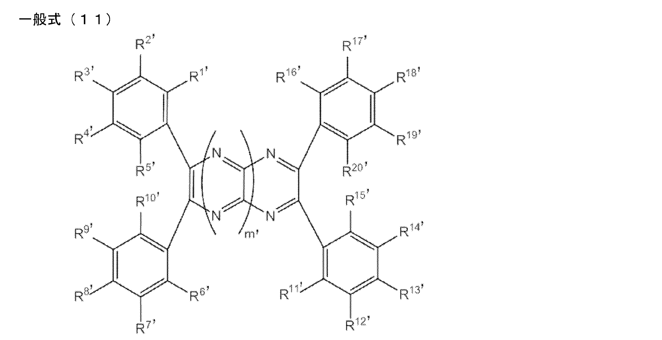
一般式(11)におけるR1'~R5'、R6'~R20'、m'の説明と好ましい範囲については、一般式(1)で表される化合物の説明を参照することができる。

R1a~R5aおよびR16a~R19aが採りうる置換基の説明と好ましい例については、一般式(1)のR1~R5が採りうる置換基の説明と好ましい例を参照することができ、このうちR1a~R5aが採る置換基はフッ素原子であることが好ましい。R6a~R15aが採りうるN,N-ジアリールアミノ基の説明と好ましい範囲については、一般式(1)のR6~R20が採りうるN,N-ジアリールアミノ基の説明と好ましい範囲を参照することができる。nは1または2であり、1であることが好ましい。Zが炭素鎖であるとき、炭素鎖の炭素数は1または2である。炭素数が2であるとき、炭素原子の間には不飽和結合が存在していてよい。また、炭素鎖は置換基で置換されていてもよい。この置換基の説明と好ましい範囲については、一般式(2)のAr1およびAr2が採りうる置換芳香族基等の置換基の説明と好ましい範囲を参照することができる。
一般式(11)で表される化合物の合成法は特に制限されない。一般式(11)で表される化合物の合成は、既知の合成法や条件を適宜組み合わせることにより行うことができる。
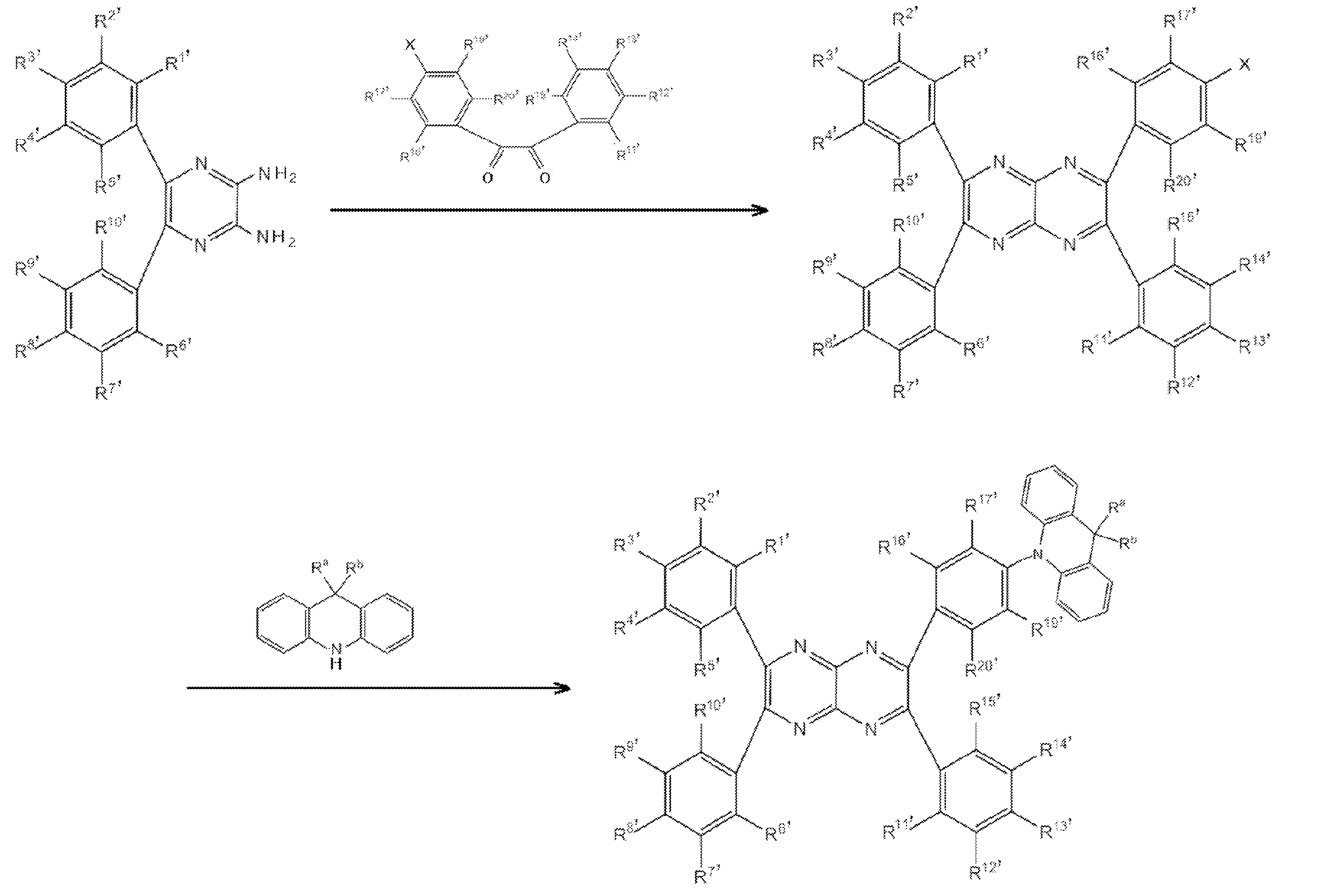
例えば、R18'が一般式(3)で表される基であり、mが1である一般式(11)で表される化合物は下記のスキームに従って合成することができる。
本発明の一般式(1)で表される化合物は、有機発光素子の発光材料として有用である。このため、本発明の一般式(1)で表される化合物は、有機発光素子の発光層に発光材料として効果的に用いることができる。一般式(1)で表される化合物の中には、遅延蛍光を放射する遅延蛍光材料(遅延蛍光体)が含まれている。すなわち本発明は、一般式(1)で表される構造を有する遅延蛍光体の発明と、一般式(1)で表される化合物を遅延蛍光体として使用する発明と、一般式(1)で表される化合物を用いて遅延蛍光を発光させる方法の発明も提供する。そのような化合物を発光材料として用いた有機発光素子は、遅延蛍光を放射し、発光効率が高いという特徴を有する。その原理を、有機エレクトロルミネッセンス素子を例にとって説明すると以下のようになる。
有機フォトルミネッセンス素子は、基板上に少なくとも発光層を形成した構造を有する。また、有機エレクトロルミネッセンス素子は、少なくとも陽極、陰極、および陽極と陰極の間に有機層を形成した構造を有する。有機層は、少なくとも発光層を含むものであり、発光層のみからなるものであってもよいし、発光層の他に1層以上の有機層を有するものであってもよい。そのような他の有機層として、正孔輸送層、正孔注入層、電子阻止層、正孔阻止層、電子注入層、電子輸送層、励起子阻止層などを挙げることができる。正孔輸送層は正孔注入機能を有した正孔注入輸送層でもよく、電子輸送層は電子注入機能を有した電子注入輸送層でもよい。具体的な有機エレクトロルミネッセンス素子の構造例を図1に示す。図1において、1は基板、2は陽極、3は正孔注入層、4は正孔輸送層、5は発光層、6は電子輸送層、7は陰極を表わす。
以下において、有機エレクトロルミネッセンス素子の各部材および各層について説明する。なお、基板と発光層の説明は有機フォトルミネッセンス素子の基板と発光層にも該当する。
本発明の有機エレクトロルミネッセンス素子は、基板に支持されていることが好ましい。この基板については、特に制限はなく、従来から有機エレクトロルミネッセンス素子に慣用されているものであればよく、例えば、ガラス、透明プラスチック、石英、シリコンなどからなるものを用いることができる。
有機エレクトロルミネッセンス素子における陽極としては、仕事関数の大きい(4eV以上)金属、合金、電気伝導性化合物およびこれらの混合物を電極材料とするものが好ましく用いられる。このような電極材料の具体例としてはAu等の金属、CuI、インジウムチンオキシド(ITO)、SnO2、ZnO等の導電性透明材料が挙げられる。また、IDIXO(In2O3-ZnO)等非晶質で透明導電膜を作製可能な材料を用いてもよい。陽極はこれらの電極材料を蒸着やスパッタリング等の方法により、薄膜を形成させ、フォトリソグラフィー法で所望の形状のパターンを形成してもよく、あるいはパターン精度をあまり必要としない場合は(100μm以上程度)、上記電極材料の蒸着やスパッタリング時に所望の形状のマスクを介してパターンを形成してもよい。あるいは、有機導電性化合物のように塗布可能な材料を用いる場合には、印刷方式、コーティング方式等湿式成膜法を用いることもできる。この陽極より発光を取り出す場合には、透過率を10%より大きくすることが望ましく、また陽極としてのシート抵抗は数百Ω/□以下が好ましい。さらに膜厚は材料にもよるが、通常10~1000nm、好ましくは10~200nmの範囲で選ばれる。
一方、陰極としては、仕事関数の小さい(4eV以下)金属(電子注入性金属と称する)、合金、電気伝導性化合物およびこれらの混合物を電極材料とするものが用いられる。このような電極材料の具体例としては、ナトリウム、ナトリウム-カリウム合金、マグネシウム、リチウム、マグネシウム/銅混合物、マグネシウム/銀混合物、マグネシウム/アルミニウム混合物、マグネシウム/インジウム混合物、アルミニウム/酸化アルミニウム(Al2O3)混合物、インジウム、リチウム/アルミニウム混合物、希土類金属等が挙げられる。これらの中で、電子注入性および酸化等に対する耐久性の点から、電子注入性金属とこれより仕事関数の値が大きく安定な金属である第二金属との混合物、例えば、マグネシウム/銀混合物、マグネシウム/アルミニウム混合物、マグネシウム/インジウム混合物、アルミニウム/酸化アルミニウム(Al2O3)混合物、リチウム/アルミニウム混合物、アルミニウム等が好適である。陰極はこれらの電極材料を蒸着やスパッタリング等の方法により薄膜を形成させることにより、作製することができる。また、陰極としてのシート抵抗は数百Ω/□以下が好ましく、膜厚は通常10nm~5μm、好ましくは50~200nmの範囲で選ばれる。なお、発光した光を透過させるため、有機エレクトロルミネッセンス素子の陽極または陰極のいずれか一方が、透明または半透明であれば発光輝度が向上し好都合である。
また、陽極の説明で挙げた導電性透明材料を陰極に用いることで、透明または半透明の陰極を作製することができ、これを応用することで陽極と陰極の両方が透過性を有する素子を作製することができる。
発光層は、陽極および陰極のそれぞれから注入された正孔および電子が再結合することにより励起子が生成した後、発光する層であり、発光材料を単独で発光層に使用しても良いが、好ましくは発光材料とホスト材料を含む。発光材料としては、一般式(1)で表される本発明の化合物群から選ばれる1種または2種以上を用いることができる。本発明の有機エレクトロルミネッセンス素子および有機フォトルミネッセンス素子が高い発光効率を発現するためには、発光材料に生成した一重項励起子および三重項励起子を、発光材料中に閉じ込めることが重要である。従って、発光層中に発光材料に加えてホスト材料を用いることが好ましい。ホスト材料としては、励起一重項エネルギー、励起三重項エネルギーの少なくとも何れか一方が本発明の発光材料よりも高い値を有する有機化合物を用いることができる。その結果、本発明の発光材料に生成した一重項励起子および三重項励起子を、本発明の発光材料の分子中に閉じ込めることが可能となり、その発光効率を十分に引き出すことが可能となる。もっとも、一重項励起子および三重項励起子を十分に閉じ込めることができなくても、高い発光効率を得ることが可能な場合もあるため、高い発光効率を実現しうるホスト材料であれば特に制約なく本発明に用いることができる。本発明の有機発光素子または有機エレクトロルミネッセンス素子において、発光は発光層に含まれる本発明の発光材料から生じる。この発光は蛍光発光および遅延蛍光発光の両方を含む。但し、発光の一部或いは部分的にホスト材料からの発光があってもかまわない。
ホスト材料を用いる場合、発光材料である本発明の化合物が発光層中に含有される量は0.1重量%以上であることが好ましく、1重量%以上であることがより好ましく、また、50重量%以下であることが好ましく、20重量%以下であることがより好ましく、10重量%以下であることがさらに好ましい。
発光層におけるホスト材料としては、正孔輸送能、電子輸送能を有し、かつ発光の長波長化を防ぎ、なおかつ高いガラス転移温度を有する有機化合物であることが好ましい。
注入層とは、駆動電圧低下や発光輝度向上のために電極と有機層間に設けられる層のことで、正孔注入層と電子注入層があり、陽極と発光層または正孔輸送層の間、および陰極と発光層または電子輸送層との間に存在させてもよい。注入層は必要に応じて設けることができる。
阻止層は、発光層中に存在する電荷(電子もしくは正孔)および/または励起子の発光層外への拡散を阻止することができる層である。電子阻止層は、発光層および正孔輸送層の間に配置されることができ、電子が正孔輸送層の方に向かって発光層を通過することを阻止する。同様に、正孔阻止層は発光層および電子輸送層の間に配置されることができ、正孔が電子輸送層の方に向かって発光層を通過することを阻止する。阻止層はまた、励起子が発光層の外側に拡散することを阻止するために用いることができる。すなわち電子阻止層、正孔阻止層はそれぞれ励起子阻止層としての機能も兼ね備えることができる。本明細書でいう電子阻止層または励起子阻止層は、一つの層で電子阻止層および励起子阻止層の機能を有する層を含む意味で使用される。
正孔阻止層とは広い意味では電子輸送層の機能を有する。正孔阻止層は電子を輸送しつつ、正孔が電子輸送層へ到達することを阻止する役割があり、これにより発光層中での電子と正孔の再結合確率を向上させることができる。正孔阻止層の材料としては、後述する電子輸送層の材料を必要に応じて用いることができる。
電子阻止層とは、広い意味では正孔を輸送する機能を有する。電子阻止層は正孔を輸送しつつ、電子が正孔輸送層へ到達することを阻止する役割があり、これにより発光層中での電子と正孔が再結合する確率を向上させることができる。
励起子阻止層とは、発光層内で正孔と電子が再結合することにより生じた励起子が電荷輸送層に拡散することを阻止するための層であり、本層の挿入により励起子を効率的に発光層内に閉じ込めることが可能となり、素子の発光効率を向上させることができる。励起子阻止層は発光層に隣接して陽極側、陰極側のいずれにも挿入することができ、両方同時に挿入することも可能である。すなわち、励起子阻止層を陽極側に有する場合、正孔輸送層と発光層の間に、発光層に隣接して該層を挿入することができ、陰極側に挿入する場合、発光層と陰極との間に、発光層に隣接して該層を挿入することができる。また、陽極と、発光層の陽極側に隣接する励起子阻止層との間には、正孔注入層や電子阻止層などを有することができ、陰極と、発光層の陰極側に隣接する励起子阻止層との間には、電子注入層、電子輸送層、正孔阻止層などを有することができる。阻止層を配置する場合、阻止層として用いる材料の励起一重項エネルギーおよび励起三重項エネルギーの少なくともいずれか一方は、発光材料の励起一重項エネルギーおよび励起三重項エネルギーよりも高いことが好ましい。
正孔輸送層とは正孔を輸送する機能を有する正孔輸送材料からなり、正孔輸送層は単層または複数層設けることができる。
正孔輸送材料としては、正孔の注入または輸送、電子の障壁性のいずれかを有するものであり、有機物、無機物のいずれであってもよい。使用できる公知の正孔輸送材料としては例えば、トリアゾール誘導体、オキサジアゾール誘導体、イミダゾール誘導体、カルバゾール誘導体、インドロカルバゾール誘導体、ポリアリールアルカン誘導体、ピラゾリン誘導体およびピラゾロン誘導体、フェニレンジアミン誘導体、アリールアミン誘導体、アミノ置換カルコン誘導体、オキサゾール誘導体、スチリルアントラセン誘導体、フルオレノン誘導体、ヒドラゾン誘導体、スチルベン誘導体、シラザン誘導体、アニリン系共重合体、また導電性高分子オリゴマー、特にチオフェンオリゴマー等が挙げられるが、ポルフィリン化合物、芳香族第3級アミン化合物およびスチリルアミン化合物を用いることが好ましく、芳香族第3級アミン化合物を用いることがより好ましい。
電子輸送層とは電子を輸送する機能を有する材料からなり、電子輸送層は単層または複数層設けることができる。
電子輸送材料(正孔阻止材料を兼ねる場合もある)としては、陰極より注入された電子を発光層に伝達する機能を有していればよい。使用できる電子輸送層としては例えば、ニトロ置換フルオレン誘導体、ジフェニルキノン誘導体、チオピランジオキシド誘導体、カルボジイミド、フレオレニリデンメタン誘導体、アントラキノジメタンおよびアントロン誘導体、オキサジアゾール誘導体等が挙げられる。さらに、上記オキサジアゾール誘導体において、オキサジアゾール環の酸素原子を硫黄原子に置換したチアジアゾール誘導体、電子吸引基として知られているキノキサリン環を有するキノキサリン誘導体も、電子輸送材料として用いることができる。さらにこれらの材料を高分子鎖に導入した、またはこれらの材料を高分子の主鎖とした高分子材料を用いることもできる。


一方、りん光については、本発明の化合物のような通常の有機化合物では、励起三重項エネルギーは不安定で熱等に変換され、寿命が短く直ちに失活するため、室温では殆ど観測できない。通常の有機化合物の励起三重項エネルギーを測定するためには、極低温の条件での発光を観測することにより測定可能である。
(1)一重項エネルギーES1
測定対象化合物とmCBPとを、測定対象化合物が濃度6重量%となるように共蒸着することでSi基板上に厚さ100nmの試料を作製した。常温(300K)でこの試料の蛍光スペクトルを測定した。励起光入射直後から入射後100ナノ秒までの発光を積算することで、縦軸を発光強度、横軸を波長の蛍光スペクトルを得た。蛍光スペクトルは、縦軸を発光、横軸を波長とした。この発光スペクトルの短波側の立ち上がりに対して接線を引き、その接線と横軸との交点の波長値 λedge[nm]を求めた。この波長値を次に示す換算式でエネルギー値に換算した値をES1とした。
換算式:ES1[eV]=1239.85/λedge
発光スペクトルの測定には、励起光源に窒素レーザー(Lasertechnik Berlin社製、MNL200)を検出器には、ストリークカメラ(浜松ホトニクス社製、C4334)を用いた。
(2) 三重項エネルギーET1
一重項エネルギーES1と同じ試料を5[K]に冷却し、励起光(337nm)を燐光測定用試料に照射し、ストリークカメラを用いて、燐光強度を測定した。励起光入射後1ミリ秒から入射後10ミリ秒の発光を積算することで、縦軸を発光強度、横軸を波長の燐光スペクトルを得た。この燐光スペクトルの短波長側の立ち上がりに対して接線を引き、その接線と横軸との交点の波長値λedge[nm]を求めた。この波長値を次に示す換算式でエネルギー値に換算した値をET1とした。
換算式:ET1[eV]=1239.85/λedge
燐光スペクトルの短波長側の立ち上がりに対する接線は以下のように引いた。燐光スペクトルの短波長側から、スペクトルの極大値のうち、最も短波長側の極大値までスペクトル曲線上を移動する際に、長波長側に向けて曲線上の各点における接線を考える。この接線は、曲線が立ち上がるにつれ(つまり縦軸が増加するにつれ)、傾きが増加する。この傾きの値が極大値をとる点において引いた接線を、当該燐光スペクトルの短波長側の立ち上がりに対する接線とした。
なお、スペクトルの最大ピーク強度の10%以下のピーク強度をもつ極大点は、上述の最も短波長側の極大値には含めず、最も短波長側の極大値に最も近い、傾きの値が極大値をとる点において引いた接線を当該燐光スペクトルの短波長側の立ち上がりに対する接線とした。
本合成例において、以下のスキームにしたがって、例示化合物(1)を合成した。

J.Chem.Research(s),1997,250-251に記載の方法に基づき、以下の方法で2,3-ジアミノ-5,6-ジフェニルピラジンを合成した。
3,4-ジアミノ-1,2,5-チアジアゾール(7.9g,68.2mmol)、ベンジル(15.8g,75.0mmol)、酢酸230mlを500ml三口フラスコに投入し、還流により5時間撹拌した。反応溶液を室温まで放冷した後、溶媒を留去し、カラムクロマトグラフィーを用いて精製を行うことにより、5,6-ジフェニル[1,2,5]チアジアゾロ[3,4-b]ピラジンを収量8.0g、収率41%で得た。
次に、5,6-ジフェニル[1,2,5]チアジアゾロ[3,4-b]ピラジン(8.0g,27.7mmol)、塩化スズ(II)二水和物(31.2g,138.5mmol)、メタノール160mlを1000ml三口フラスコに投入した後、濃塩酸160mlをゆっくりと加え、窒素気流下、60℃で2時間撹拌した。室温まで放冷した溶液を、飽和炭酸ナトリウム水溶液を用いてpH8~9まで中和した後、溶液内のメタノールをある程度留去した。沈殿物を濾取し、酢酸エチルを用いて固体抽出を3回繰り返した後、カラムクロマトグラフィーで精製を行うことにより、2,3-ジアミノ-5,6-ジフェニルピラジンを収量4.8g、収率66%で得た。
2,3-ジアミノ-5,6-ジフェニルピラジン(1.0g,3.8mmol)と、Eur.J.Org.Chem.,2012,320-328に記載の方法で合成した1-(4-ブロモフェニル)-2-フェニルエタン-1,2-ジオン(1.2g,4.2mmol)、酢酸30mlを100ml三口フラスコに投入し、4時間加熱還流撹拌した。溶液を室温まで放冷した後、溶媒を留去し、カラムクロマトグラフィーを用いて精製を行うことにより、中間体Bを収量1.6g、収率88 %で得た。
Eur.J.Inorg.Chem.,2006,3676-3683に記載の方法に基づき、以下の方法で例示化合物(1)を合成した。
中間体B(0.39mmol)、国際公開WO2012/039561号に記載の方法で合成した9,9-ジメチル-9,10-ジヒドロアクリジン(89mg,0.43mmol)と、トリス(ジベンジリデンアセトン)ジパラジウム(0)(36mg,0.039mmol)、ナトリウムtert-ブトキシド(41mg,0.43mmol)、トルエン20ml、トリ(tert-ブチル)ホスフィン(10mg,0.050mmol)を100ml三口フラスコに投入し、撹拌しながら手早く脱気と窒素置換を3回繰り返した。この混合物を、窒素気流下、還流により8時間撹拌した。反応後、室温まで放冷した反応溶液に水を加え、ジクロロメタンで抽出、飽和食塩水で洗浄した。有機層を硫酸ナトリウムで乾燥した後、溶媒を留去し、カラムクロマトグラフィーを用いて精製を行うことにより、例示化合物(1)を収量173mg、収率69%で得た。
融点300℃以上。1H-NMR(δppm,CDCl3)1.69(6H,s),6.31(2H,dd,J=8.4,1.2),6.96(2H,td,J=7.2,0.12),7.33~7.48(13H,m),7.71(4H,d,J=7.6),7.77(2H,d,J=8.0),7.91(2H,d,J=8.0)
本合成例において、以下のスキームにしたがって、例示化合物(2)を合成した。

3,4-ジアミノ-1,2,5-チアジアゾール(9.9g,85.2mmol)、4,4’-ジブロモベンジル(24.4g,66.4mmol)、酢酸300mlを1000ml三口フラスコに投入し、還流により24時間撹拌した。反応溶液を室温まで放冷した後、溶媒を留去し、カラムクロマトグラフィーを用いて精製を行うことにより、中間体Cを収量19.0g、収率64%で得た。
中間体C(21.4g,47.8mmol)、塩化スズ(II)二水和物(50.3g,,222.9mmol)、メタノール400mlを1000ml三口フラスコに投入した後、濃塩酸400mlをゆっくりと加え、窒素気流下、60℃で3時間撹拌した。室温まで放冷した溶液を、飽和炭酸ナトリウム水溶液を用いてpH8~9まで中和した後、溶液内のメタノールをある程度留去した。沈殿物を濾取し、酢酸エチルを用いて固体抽出を3回繰り返した後、カラムクロマトグラフィーで精製を行うことにより、中間体Dを収量12.0g、収率60%で得た。
中間体D(0.6g,1.4mmol)、ベンジル(0.33g,1.6mmol)、酢酸10mlを50ml三口フラスコに投入し、還流により4時間撹拌した。溶液を室温まで放冷した後、溶媒を留去し、カラムクロマトグラフィーを用いて精製を行うことにより、中間体Eを収量0.62g、収率73%で得た。
中間体B(0.39mmol)の代わりに中間体E(0.39mmol)を用い、9,9-ジメチル-9,10-ジヒドロアクリジンを2倍モル量用いる以外は、合成例1の工程(3)と同様の工程を行うことにより、例示化合物(2)を収量0.24g、収率50%で得た。
融点300℃以上。1H-NMR(δppm,CDCl3)1.69(12H),6.33(4H,m),6.90(8H,m),7.37~7.53(14H,m),7.74(4H,m),8.01(4H,d,J=8.0)
本合成例において、以下のスキームにしたがって、例示化合物(4)を合成した。
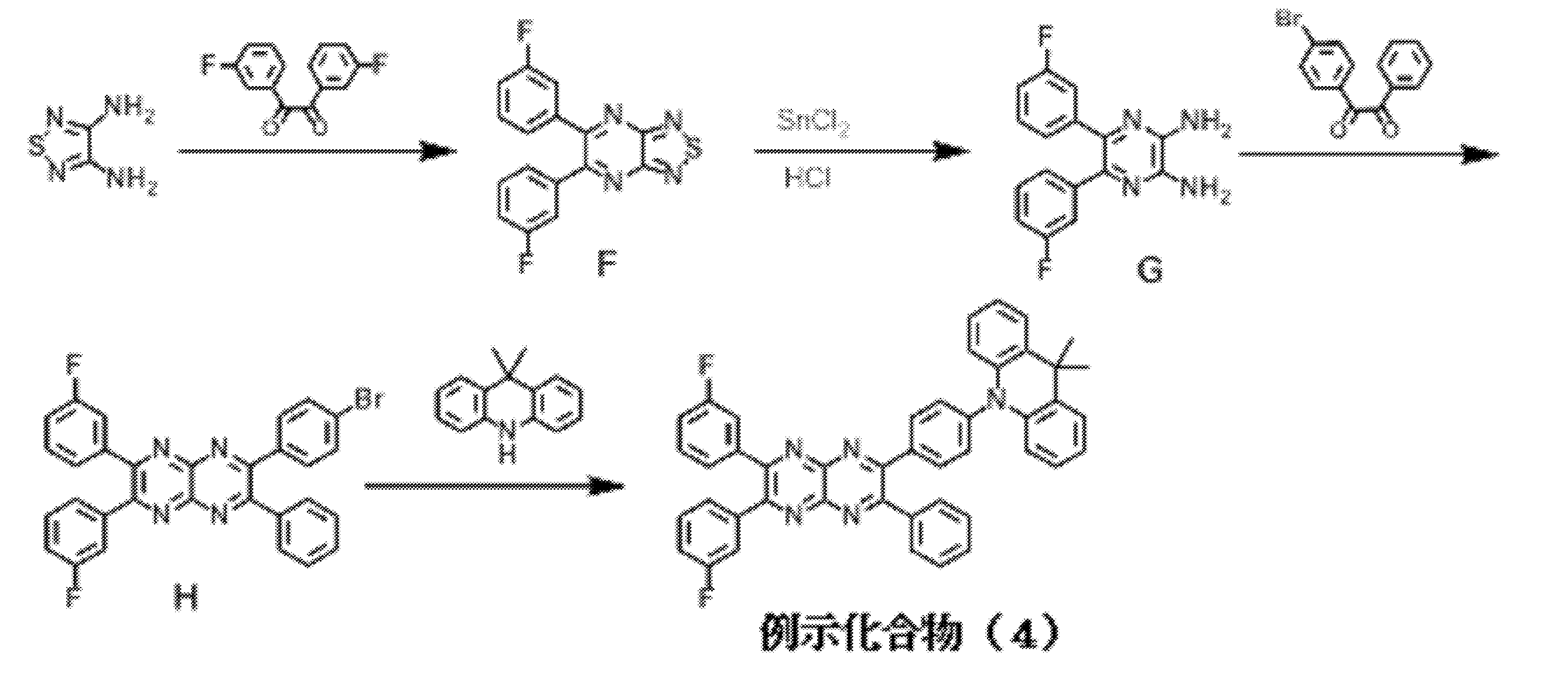
3,4-ジアミノ-1,2,5-チアジアゾール(9.9g,85.2mmol)と、Bioorgnic & Medicinal Chem.2007,15,3801-3817に記載の方法で合成した3,3’-ジフルオロベンジル(16.3g,66.4mmol)、酢酸300mlを1000ml三口フラスコに投入し、還流により24時間撹拌した。溶液を室温まで放冷した後、溶媒を留去し、カラムクロマトグラフィ―を用いて精製を行うことにより、中間体Fを収量18.1g、収率65%で得た。
中間体F(15.6g,47.8mmol)、塩化スズ(II)二水和物(50.3g,222.9mmol)、メタノール400mlを1000ml三口フラスコに投入した後、濃塩酸400mlをゆっくりと加え、窒素気流下、60℃で3時間撹拌した。室温まで放冷した溶液を、飽和炭酸ナトリウム水溶液を用いてpH8~9まで中和した後、溶液内のメタノールをある程度留去した。沈殿物を濾取し、酢酸エチルを用いて固体抽出を3回繰り返した後、カラムクロマトグラフィーで精製を行うことにより、中間体Gを収量8.6g、収率60%で得た。
中間体G(0.60g,1.4mmol)、4-ブロモベンジル(0.46g,1.6mmol)、酢酸10mlを50ml三口フラスコに投入し、還流により4時間撹拌した。溶液を室温まで放冷した後、溶媒を留去し、カラムクロマトグラフィーを用いて精製を行うことにより、中間体Hを収量0.56g、収率73%で得た。
中間体B(0.39mmol)の代わりに中間体H(0.39mmol)を用い、9,9-ジメチル-9,10-ジヒドロアクリジンを2倍モル量用いる以外は、合成例1の工程(3)と同様の工程を行うことにより、例示化合物(4)を収量0.15g、収率55%で得た。
融点300℃以上。
本合成例において、以下のスキームにしたがって、例示化合物(7)を合成した。

3,4-ジアミノ-1,2,5-チアジアゾール(10.0g,86.1mmol)、Bioorgnic & Medicinal Chem.2007,15,3801-3817に記載の方法で合成した3,3’-ジフルオロベンジル(16.5g,67.2mmol)、酢酸300mlを1000ml三口フラスコに投入し、還流により24時間撹拌した。溶液を室温まで放冷した後、溶媒を留去し、カラムクロマトグラフィーを用いて精製を行うことにより、中間体Iを収量14.6g、収率65%で得た。
中間体I(21.4g,47.8mmol)、塩化スズ(II)二水和物(50.3g,222.9mmol)、メタノール400mlを1000ml三口フラスコに投入した後、濃塩酸400mlをゆっくりと加え、窒素気流下、60℃で3時間撹拌した。室温まで放冷した溶液を、飽和炭酸ナトリウム水溶液を用いてpH8~9まで中和した後、溶液内のメタノールをある程度留去した。沈殿物を濾取し、酢酸エチルを用いて固体抽出を3回繰り返した後、カラムクロマトグラフィーで精製を行うことにより、中間体Jを収量9.6g、収率60%で得た。
中間体J(0.6g,1.8mmol)、4-ブロモベンジル(0.58g,2.0mmol)、酢酸10mlを50ml三口フラスコに投入し、還流で4時間撹拌した。溶液を室温まで放冷した後、溶媒を留去し、カラムクロマトグラフィーを用いて精製を行うことにより、中間体Kを収量0.78g、収率73%で得た。
中間体B(0.39mmol)の代わりに中間体K(0.39mmol)を用いる以外は合成例1の工程(3)と同様の工程を行うことにより、例示化合物(7)を収量0.14g、収率50%で得た。
融点300℃以上。
合成例1で合成した中間体B(0.2g,0.39mmol)、フェノキサジン(78mg,0.43mmol)、酢酸パラジウム(II)(5mg,0.023mmol)、炭酸カリウム(0.16g,1.16mmol)、トルエン20ml、トリ(tert-ブチル)ホスフィン(17mg,0.085mmol)を100ml三口フラスコに投入し、撹拌しながら手早く脱気と窒素置換を3回繰り返した。この混合物を、窒素気流下、還流により10時間撹拌した。反応後、室温まで放冷した反応溶液に水を加え、ジクロロメタンで抽出、飽和食塩水で洗浄した。有機層を硫酸ナトリウムで乾燥した後、溶媒を留去し、カラムクロマトグラフィーを用いて精製を行うことにより、例示化合物(11)を収量0.14g、収率59%で得た。
融点300℃以上。1H-NMR(δppm,CDCl3)5.96(2H,dd,J=8.0,1.6),6.60~6.78(6H,m),7.33~7.53(12H,m),7.67~7.80(6H,m),7.87(2H,d,J=8.0)
合成例2で合成した中間体E(0.2g,0.34mmol)、フェノキサジン(0.14g,0.74mmol)、酢酸パラジウム(II)(5mg,0.020mmol)、炭酸カリウム(0.28g,2.02mmol)、トルエン20ml、トリ(tert-ブチル)ホスフィン(15mg,0.074mmol)を100ml三口フラスコに投入し、撹拌しながら手早く脱気と窒素置換を3回繰り返した。混合物を、窒素気流下、還流により9時間撹拌した。反応後、室温まで放冷した反応溶液に水を加え、ジクロロメタンで抽出、飽和食塩水で洗浄した。有機層を硫酸ナトリウムで乾燥した後、溶媒を留去し、カラムクロマトグラフィーを用いて精製を行うことにより、例示化合物(12)を収量0.19g、収率71%で得た。
融点300℃以上。
1H-NMR(δppm,CDCl3)5.96(4H,dd,J=8.0,1.6),6.53(4H,td,J-=8.0,1.6),6.66(4H,td,J=8.0,1.6),6.71(4H,dd,J=8.0,1.6),7.37~7.48(10H,m),7.72(4H,d,J=7.2),7.95(4H,d,J=8.8)
本合成例において、以下のスキームにしたがって、例示化合物(25)を合成した。
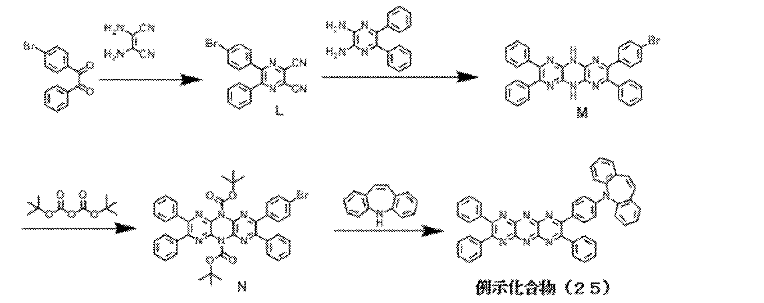
4-ブロモベンジル(7.9g,27.2mmol)、ジアミノマレオニトリル(3.5g,32.6mmol)、酢酸120mlを500ml三口フラスコに投入し、還流により4時間撹拌した。反応終了後、反応液を放冷し、溶媒を留去した後、カラムクロマトグラフィーで精製することにより、中間体Lを収量9.8g、収率93%で得た。
中間体L(1.9g,5.2mmol)、2,3-ジアミノ-5,6-ジフェニルピラジン(1.0g,5.8mmol)、炭酸カリウム(1.3g,9.5mmol)、ジメチルスルホキシド30mlを100ml三口フラスコに投入した後、脱気と窒素置換を3回繰り返した。混合溶液を、窒素気流下、120℃で7時間撹拌した。反応液を放冷した後、ジクロロメタン、蒸留水で抽出を行った。有機層と亜ジチオン酸ナトリウム水溶液を分液漏斗に注入して分液し、その有機層を硫酸ナトリウムで乾燥した後、カラムクロマトグラフィーで精製することにより、中間体Mを収量0.89g、収率30%で得た。
中間体M(0.63g,1.1mmol)、二炭酸ジ-tert-ブチル(0.52g,2.4mmol)、トリエチルアミン(0.24g,2.37mmol)、N,N-ジメチル-4-アミノピリジン(26mg,0.22mmol)、テトラヒドロフラン30mlを100mlフラスコに投入し、室温で7時間撹拌した。反応後、反応液から溶媒を留去し、その残留物に20~30ml程度の酢酸エチルを加え、濾過することで不純物を濾液側に除去した。得られた残留物をカラムクロマトグラフィーで精製することにより、中間体Nを収量0.56g、収率66%で得た。
中間体N(0.31g,0.40mmol)、イミノスチルベン(0.12g,0.60mmol)、トリス(ジベンジリデンアセトン)ジパラジウム(0)(36mg,0.040mmol)、ナトリウムtert-ブトキシド(0.57g,5.96mmol)、トルエン20ml、トリ(tert-ブチル)ホスフィン(10mg,0.052mmol)を100ml三口フラスコに投入し、撹拌しながら手早く脱気と窒素置換を3回繰り返した。混合物を、窒素気流下、還流により26時間撹拌した。反応後、室温まで放冷した反応溶液に水を加え、ジクロロメタンで抽出、飽和食塩水で洗浄した。有機層を硫酸ナトリウムで乾燥した後、溶媒を留去し、カラムクロマトグラフィーを用いて精製を行うことにより、例示化合物(25)を収量0.13g、収率46%で得た。
融点300℃以上。
合成例1で合成した例示化合物(1)のトルエン溶液(濃度10-5M)を調製した。
このトルエン溶液について380nm励起光によるフォトルミネッセンス量子効率を測定したところ、フォトルミネッセンス量子効率は、バブリングを行わないトルエン溶液で12.5%、窒素バブリングを行ったトルエン溶液で33.4%であった。
また、このトルエン溶液について、400nm励起光による発光スペクトルと紫外線吸収スペクトルを測定した結果を図2に示す。最大発光波長λmaxは651nmであった。
340nm励起光による過渡減衰曲線を測定した結果を図3に示す。過渡減衰曲線は、化合物に励起光を当てて発光強度が失活してゆく過程を測定した発光寿命測定結果を示すものである。通常の一成分の発光(蛍光もしくはリン光)では発光強度は単一指数関数的に減衰する。これは、グラフの縦軸がセミlog である場合には、直線的に減衰することを意味している。図3に示す例示化合物(1)の過渡減衰曲線では、観測初期にこのような直線的成分(蛍光)が観測されているが、数μ秒以降には直線性から外れる成分が現れている。これは遅延成分の発光であり、初期の成分と加算される信号は、長時間側に裾をひくゆるい曲線になる。このように発光寿命を測定することによって、例示化合物(1)は蛍光成分のほかに遅延成分を含む発光体であることが確認された。
発光寿命は、バブリングを行わないトルエン溶液で0.37μs、窒素バブリングを行ったトルエン溶液で36.1μsであった。
このトルエン溶液の励起一重項状態と励起三重項状態のエネルギー差ΔEstは0.002eVであり、S0→S1遷移についての頻度因子であるf値は0.0002であった。ΔEst値は熱活性化の起き易さの尺度として用い、この値が小さいほど熱活性化遅延蛍光がおきやすい可能性があると考えた。またf値は、S0(基底状態)からS1(励起一重項状態)への遷移の起きやすさであるが、今回の計算では発光の起き易さ(蛍光強度)の尺度としてf値を用い、この値が大きいほど強い蛍光を示す可能性があると考えた。
合成例2で合成した例示化合物(2)のトルエン溶液(濃度10-5M)を調製した。
このトルエン溶液について440nm励起光によるフォトルミネッセンス量子効率を測定したところ、フォトルミネッセンス量子効率は、バブリングを行わないトルエン溶液で12.0%、窒素バブリングを行ったトルエン溶液で32.4%であった。
また、このトルエン溶液について、444nm励起光による発光スペクトルと紫外線吸収スペクトルを測定した結果を図4に示し、340nm励起光による過渡減衰曲線を測定した結果を図5に示す。図4から、最大発光波長λmaxは621nmであった。図5から、発光寿命の短い成分(即時蛍光成分)と発光寿命が長い成分(遅延蛍光成分)を観測することができ、遅延蛍光成分の発光寿命は、バブリングを行わないトルエン溶液で0.40μs、窒素バブリングを行ったトルエン溶液で23.5μsであった。また、このトルエン溶液の励起一重項状態と励起三重項状態のエネルギー差ΔEstは0.002eVであり、f値は0であった。
比較化合物(A)のトルエン溶液(濃度10-5M)を調製した。
このトルエン溶液について特性を評価したところ、320nm励起光によるフォトルミネッセンス量子効率は、バブリングを行わないトルエン溶液で1.2%、窒素バブリングを行ったトルエン溶液で2.3%であり、最大発光波長は706nmであった。また、励起一重項状態と励起三重項状態のエネルギー差ΔEstは0.047eVであり、f値は0.031であった。この比較化合物(A)のトルエン溶液は、発光が弱く、遅延蛍光を確認することができなかった。
比較化合物(B)のトルエン溶液(濃度10-5M)を調製した。
このトルエン溶液について特性を評価したところ、360nm励起光によるフォトルミネッセンス量子効率は、バブリングを行わないトルエン溶液で1.1%、窒素バブリングを行ったトルエン溶液で2.3%であり、最大発光波長は697nmであった。また、励起一重項状態と励起三重項状態のエネルギー差ΔEstは0.006eVであり、fは0.041であった。この比較化合物(B)のトルエン溶液は、発光が弱く、遅延蛍光を確認することができなかった。
比較化合物(C)のトルエン溶液(濃度10-5M)を調製した。
このトルエン溶液を用いて360nm励起光によるフォトルミネッセンスを観測したところ、遅延蛍光は明確に確認できなかった。

シリコン基板上に真空蒸着法にて、真空度3.0×10⁻⁴Pa以下の条件にて例示化合物(2)とmCBPとを異なる蒸着源から蒸着し、例示化合物(2)の濃度が6.0重量%である薄膜を50nmの厚さで形成して薄膜型有機フォトルミネッセンス素子とした。
この薄膜型有機フォトルミネッセンス素子について、400nm励起光による発光スペクトルと紫外線吸収スペクトルを測定した結果を図6に示し、過渡減衰曲線を大気下で測定した結果を図7に示す。フォトルミネッセンス量子効率は、大気下で48.9%、窒素含有雰囲気下で50.1%であり、発光波長は586nmであった。また、図7から、発光寿命が異なる3つの成分を観測することができ、各成分の発光寿命は7.81ns、969.0ns、5.73μsであった。
膜厚100nmのインジウム・スズ酸化物(ITO)からなる陽極が形成されたガラス基板上に、各薄膜を真空蒸着法にて、真空度3.0×10⁻⁴Paで積層した。まず、ITO上にα-NPDを35nmの厚さに形成した。次に、例示化合物(2)とmCBPを異なる蒸着源から共蒸着し、15nmの厚さの層を形成して発光層とした。この時、例示化合物(2)の濃度は6.0重量%とした。次に、TPBiを65nmの厚さに形成し、さらにフッ化リチウム(LiF)を0.8nm真空蒸着し、次いでアルミニウム(Al)を100nmの厚さに蒸着することにより陰極を形成し、有機エレクトロルミネッセンス素子とした。
製造した有機エレクトロルミネッセンス素子について、1mA/cm2、10mA/cm2、100mA/cm2の各条件で測定した発光スペクトルを図8に示し、電圧-電流密度-輝度特性を図9に示し、電流密度-電流効率-電力効率特性を図10に示し、電流密度-外部量子効率特性を図11に示す。この有機エレクトロルミネッセンス素子は、ターンオン電圧が3.2V、最大輝度が14820cd/m2、最大電流効率が27.7cd/A、最大電力効率が25.1lm/Wであった。また、この有機エレクトロルミネッセンス素子は10.5%の高い外部量子収率を達成した。仮に発光量子効率が100%の蛍光材料を用いてバランスの取れた理想的な有機エレクトロルミネッセンス素子を試作したとすると、光取り出し効率が20~30%であれば、蛍光発光の外部量子効率は5~7.5%となる。この値が一般に、蛍光材料を用いた有機エレクトロルミネッセンス素子の外部量子効率の理論限界値とされている。本発明の有機エレクトロルミネッセンス素子は、理論限界値を超える高い外部量子効率を実現している点で極めて優れている。

2 陽極
3 正孔注入層
4 正孔輸送層
5 発光層
6 電子輸送層
7 陰極
Claims (13)
- 下記一般式(1)で表わされる化合物からなる発光材料。
- 前記ハメットのσp値が0以上の置換基が、ハロゲン原子、アシルオキシ基、アルコキシカルボニル基、アリールオキシカルボニル基、フェニル基またはシアノ基であることを特徴とする請求項1に記載の発光材料。
- 前記置換もしくは無置換のN,N-ジアリールアミノ基が下記一般式(2)で表される基であることを特徴とする請求項1または2に記載の発光材料。

- 前記Ar1およびAr2は直接もしくは間接に連結して環を形成していることを特徴とする請求項3に記載の発光材料。
- 前記一般式(2)で表される基が、下記一般式(3)で表されることを特徴とする請求項4に記載の発光材料。
- 前記一般式(1)において、mが1であることを特徴とする請求項1~5のいずれか1項に記載の発光材料。
- 遅延蛍光を放射することを特徴とする請求項1~6のいずれか1項に記載の発光材料。
- 下記一般式(11)で表わされる化合物。

- 一般式(11)で表わされる化合物が、下記一般式(12)で表わされることを特徴とする請求項8に記載の化合物。
- 前記R1a~R5aが、各々独立に水素原子またはフッ素原子であることを特徴とする請求項9に記載の化合物。
- 請求項1~7のいずれか1項に記載の発光材料を含む発光層を基板上に有することを特徴とする有機発光素子。
- 遅延蛍光を放射することを特徴とする請求項11に記載の有機発光素子。
- 有機エレクトロルミネッセンス素子であることを特徴とする請求項11または12に記載の有機発光素子。
Priority Applications (3)
| Application Number | Priority Date | Filing Date | Title |
|---|---|---|---|
| JP2016510197A JP6600298B2 (ja) | 2014-03-27 | 2015-03-06 | 発光材料、有機発光素子および化合物 |
| CN201580016425.4A CN106133112B (zh) | 2014-03-27 | 2015-03-06 | 发光材料、有机发光元件及化合物 |
| US15/129,070 US10256415B2 (en) | 2014-03-27 | 2015-03-06 | Light-emitting material, organic light-emitting device, and compound |
Applications Claiming Priority (2)
| Application Number | Priority Date | Filing Date | Title |
|---|---|---|---|
| JP2014-066316 | 2014-03-27 | ||
| JP2014066316 | 2014-03-27 |
Publications (1)
| Publication Number | Publication Date |
|---|---|
| WO2015146541A1 true WO2015146541A1 (ja) | 2015-10-01 |
Family
ID=54195067
Family Applications (1)
| Application Number | Title | Priority Date | Filing Date |
|---|---|---|---|
| PCT/JP2015/056623 WO2015146541A1 (ja) | 2014-03-27 | 2015-03-06 | 発光材料、有機発光素子および化合物 |
Country Status (4)
| Country | Link |
|---|---|
| US (1) | US10256415B2 (ja) |
| JP (1) | JP6600298B2 (ja) |
| CN (1) | CN106133112B (ja) |
| WO (1) | WO2015146541A1 (ja) |
Cited By (17)
| Publication number | Priority date | Publication date | Assignee | Title |
|---|---|---|---|---|
| KR20190082772A (ko) * | 2017-01-25 | 2019-07-10 | 쓰추안 날리지 익스프레스 인스티튜트 포 이노베이티브 테크놀로지스 컴퍼니 리미티드 | 짧은 방출 감쇠 시간을 갖는 직접적인 단일항 수집을 위한 유기 분자 및 광전자 장치에서의 이의 응용 |
| WO2020076796A1 (en) | 2018-10-09 | 2020-04-16 | Kyulux, Inc. | Novel composition of matter for use in organic light-emitting diodes |
| WO2021157642A1 (ja) | 2020-02-04 | 2021-08-12 | 株式会社Kyulux | ホスト材料、組成物および有機発光素子 |
| US11101440B2 (en) | 2015-07-01 | 2021-08-24 | Kyushu University, National University Corporation | Organic electroluminescent device |
| WO2021235549A1 (ja) | 2020-05-22 | 2021-11-25 | 株式会社Kyulux | 化合物、発光材料および発光素子 |
| WO2022025248A1 (ja) | 2020-07-31 | 2022-02-03 | 株式会社Kyulux | 化合物、発光材料および発光素子 |
| US11335872B2 (en) | 2016-09-06 | 2022-05-17 | Kyulux, Inc. | Organic light-emitting device |
| WO2022168956A1 (ja) | 2021-02-04 | 2022-08-11 | 株式会社Kyulux | 化合物、発光材料および有機発光素子 |
| US11476435B2 (en) | 2017-08-24 | 2022-10-18 | Kyushu University, National University Corporation | Film and organic light-emitting device containing perovskite-type compound and organic light-emitting material |
| US11482679B2 (en) | 2017-05-23 | 2022-10-25 | Kyushu University, National University Corporation | Compound, light-emitting lifetime lengthening agent, use of n-type compound, film and light-emitting device |
| WO2022244503A1 (ja) | 2021-05-20 | 2022-11-24 | 株式会社Kyulux | 有機発光素子 |
| WO2022270602A1 (ja) | 2021-06-23 | 2022-12-29 | 株式会社Kyulux | 有機発光素子および膜 |
| WO2022270354A1 (ja) | 2021-06-23 | 2022-12-29 | 株式会社Kyulux | 化合物、発光材料および有機発光素子 |
| WO2022270113A1 (ja) | 2021-06-23 | 2022-12-29 | 株式会社Kyulux | 有機エレクトロルミネッセンス素子 |
| WO2023282224A1 (ja) | 2021-07-06 | 2023-01-12 | 株式会社Kyulux | 有機発光素子およびその設計方法 |
| WO2023053835A1 (ja) | 2021-09-28 | 2023-04-06 | 株式会社Kyulux | 化合物、組成物、ホスト材料、電子障壁材料および有機発光素子 |
| US11930654B2 (en) | 2017-07-06 | 2024-03-12 | Kyulux, Inc. | Organic light-emitting element |
Citations (6)
| Publication number | Priority date | Publication date | Assignee | Title |
|---|---|---|---|---|
| JP2006232793A (ja) * | 2005-02-21 | 2006-09-07 | Makoto Tadokoro | 新規機能性電子受容体及びその機能性金属錯体高分子 |
| WO2007142216A1 (ja) * | 2006-06-05 | 2007-12-13 | Idemitsu Kosan Co., Ltd. | 有機エレクトロルミネッセンス素子及び有機エレクトロルミネッセンス素子用材料 |
| JP2010105927A (ja) * | 2008-10-28 | 2010-05-13 | Idemitsu Kosan Co Ltd | 含窒素複素環誘導体及びそれを用いた有機エレクトロルミネッセンス素子 |
| JP2013134947A (ja) * | 2011-12-27 | 2013-07-08 | Osaka Prefecture Univ | 電極活物質およびそれを含む二次電池 |
| JP2014011437A (ja) * | 2012-07-03 | 2014-01-20 | Kyushu Univ | 有機半導体デバイスおよび化合物 |
| JP2014009352A (ja) * | 2012-07-03 | 2014-01-20 | Kyushu Univ | 発光材料、化合物および有機発光素子 |
Family Cites Families (2)
| Publication number | Priority date | Publication date | Assignee | Title |
|---|---|---|---|---|
| JP5227510B2 (ja) | 2005-12-28 | 2013-07-03 | 株式会社半導体エネルギー研究所 | ピラジン誘導体、及び前記ピラジン誘導体を用いた発光素子、表示装置、電子機器 |
| WO2012039561A1 (en) | 2010-09-20 | 2012-03-29 | Rohm And Haas Electronic Materials Korea Ltd. | Novel organic electroluminescent compounds and organic electroluminescent device using the same |
-
2015
- 2015-03-06 CN CN201580016425.4A patent/CN106133112B/zh active Active
- 2015-03-06 JP JP2016510197A patent/JP6600298B2/ja active Active
- 2015-03-06 WO PCT/JP2015/056623 patent/WO2015146541A1/ja active Application Filing
- 2015-03-06 US US15/129,070 patent/US10256415B2/en active Active
Patent Citations (6)
| Publication number | Priority date | Publication date | Assignee | Title |
|---|---|---|---|---|
| JP2006232793A (ja) * | 2005-02-21 | 2006-09-07 | Makoto Tadokoro | 新規機能性電子受容体及びその機能性金属錯体高分子 |
| WO2007142216A1 (ja) * | 2006-06-05 | 2007-12-13 | Idemitsu Kosan Co., Ltd. | 有機エレクトロルミネッセンス素子及び有機エレクトロルミネッセンス素子用材料 |
| JP2010105927A (ja) * | 2008-10-28 | 2010-05-13 | Idemitsu Kosan Co Ltd | 含窒素複素環誘導体及びそれを用いた有機エレクトロルミネッセンス素子 |
| JP2013134947A (ja) * | 2011-12-27 | 2013-07-08 | Osaka Prefecture Univ | 電極活物質およびそれを含む二次電池 |
| JP2014011437A (ja) * | 2012-07-03 | 2014-01-20 | Kyushu Univ | 有機半導体デバイスおよび化合物 |
| JP2014009352A (ja) * | 2012-07-03 | 2014-01-20 | Kyushu Univ | 発光材料、化合物および有機発光素子 |
Cited By (20)
| Publication number | Priority date | Publication date | Assignee | Title |
|---|---|---|---|---|
| US11101440B2 (en) | 2015-07-01 | 2021-08-24 | Kyushu University, National University Corporation | Organic electroluminescent device |
| US11335872B2 (en) | 2016-09-06 | 2022-05-17 | Kyulux, Inc. | Organic light-emitting device |
| KR102216794B1 (ko) * | 2017-01-25 | 2021-02-17 | 쓰추안 날리지 익스프레스 인스티튜트 포 이노베이티브 테크놀로지스 컴퍼니 리미티드 | 짧은 방출 감쇠 시간을 갖는 직접적인 단일항 수집을 위한 유기 분자 및 광전자 장치에서의 이의 응용 |
| JP2020510986A (ja) * | 2017-01-25 | 2020-04-09 | 四川知本快車創新科技研究院有限公司Sichuan Knowledge Express Institute For Innovative Technologies Co, Ltd. | 短い発光減衰時間で単重捕集を直接に得るための有機分子及びその光電子機器における用途 |
| KR20190082772A (ko) * | 2017-01-25 | 2019-07-10 | 쓰추안 날리지 익스프레스 인스티튜트 포 이노베이티브 테크놀로지스 컴퍼니 리미티드 | 짧은 방출 감쇠 시간을 갖는 직접적인 단일항 수집을 위한 유기 분자 및 광전자 장치에서의 이의 응용 |
| US11482679B2 (en) | 2017-05-23 | 2022-10-25 | Kyushu University, National University Corporation | Compound, light-emitting lifetime lengthening agent, use of n-type compound, film and light-emitting device |
| US11930654B2 (en) | 2017-07-06 | 2024-03-12 | Kyulux, Inc. | Organic light-emitting element |
| US11476435B2 (en) | 2017-08-24 | 2022-10-18 | Kyushu University, National University Corporation | Film and organic light-emitting device containing perovskite-type compound and organic light-emitting material |
| WO2020076796A1 (en) | 2018-10-09 | 2020-04-16 | Kyulux, Inc. | Novel composition of matter for use in organic light-emitting diodes |
| WO2021157642A1 (ja) | 2020-02-04 | 2021-08-12 | 株式会社Kyulux | ホスト材料、組成物および有機発光素子 |
| WO2021157593A1 (ja) | 2020-02-04 | 2021-08-12 | 株式会社Kyulux | 組成物、膜、有機発光素子、発光組成物を提供する方法およびプログラム |
| WO2021235549A1 (ja) | 2020-05-22 | 2021-11-25 | 株式会社Kyulux | 化合物、発光材料および発光素子 |
| WO2022025248A1 (ja) | 2020-07-31 | 2022-02-03 | 株式会社Kyulux | 化合物、発光材料および発光素子 |
| WO2022168956A1 (ja) | 2021-02-04 | 2022-08-11 | 株式会社Kyulux | 化合物、発光材料および有機発光素子 |
| WO2022244503A1 (ja) | 2021-05-20 | 2022-11-24 | 株式会社Kyulux | 有機発光素子 |
| WO2022270602A1 (ja) | 2021-06-23 | 2022-12-29 | 株式会社Kyulux | 有機発光素子および膜 |
| WO2022270354A1 (ja) | 2021-06-23 | 2022-12-29 | 株式会社Kyulux | 化合物、発光材料および有機発光素子 |
| WO2022270113A1 (ja) | 2021-06-23 | 2022-12-29 | 株式会社Kyulux | 有機エレクトロルミネッセンス素子 |
| WO2023282224A1 (ja) | 2021-07-06 | 2023-01-12 | 株式会社Kyulux | 有機発光素子およびその設計方法 |
| WO2023053835A1 (ja) | 2021-09-28 | 2023-04-06 | 株式会社Kyulux | 化合物、組成物、ホスト材料、電子障壁材料および有機発光素子 |
Also Published As
| Publication number | Publication date |
|---|---|
| US10256415B2 (en) | 2019-04-09 |
| US20170110670A1 (en) | 2017-04-20 |
| CN106133112A (zh) | 2016-11-16 |
| CN106133112B (zh) | 2019-05-14 |
| JP6600298B2 (ja) | 2019-10-30 |
| JPWO2015146541A1 (ja) | 2017-04-13 |
Similar Documents
| Publication | Publication Date | Title |
|---|---|---|
| JP6600298B2 (ja) | 発光材料、有機発光素子および化合物 | |
| JP6318155B2 (ja) | 化合物、発光材料および有機発光素子 | |
| JP6493220B2 (ja) | 発光材料、有機発光素子および化合物 | |
| JP5679496B2 (ja) | 有機発光素子ならびにそれに用いる遅延蛍光材料および化合物 | |
| CN108473424B (zh) | 化合物、发光材料及有机发光元件 | |
| JP6466913B2 (ja) | 発光材料、有機発光素子および化合物 | |
| JP6277182B2 (ja) | 化合物、発光材料および有機発光素子 | |
| JP6225111B2 (ja) | 発光材料、化合物、およびそれらを用いた有機発光素子 | |
| JP5594750B2 (ja) | 化合物、発光材料および有機発光素子 | |
| JP6263524B2 (ja) | 化合物、発光材料および有機発光素子 | |
| JP6293417B2 (ja) | 化合物、発光材料および有機発光素子 | |
| JP6326050B2 (ja) | 化合物、発光材料および有機発光素子 | |
| WO2018159662A1 (ja) | 化合物、発光材料および有機発光素子 | |
| JP5366106B1 (ja) | 有機発光素子ならびにそれに用いる発光材料および化合物 | |
| JP6367189B2 (ja) | 発光材料、有機発光素子および化合物 | |
| WO2013154064A1 (ja) | 有機発光素子ならびにそれに用いる発光材料および化合物 | |
| JP2014009352A (ja) | 発光材料、化合物および有機発光素子 | |
| JP2014009224A (ja) | 発光材料、化合物および有機発光素子 | |
| JPWO2013161437A1 (ja) | 発光材料および有機発光素子 | |
| JP2017103440A (ja) | 有機発光素子ならびにそれに用いる発光材料および化合物 | |
| JP2016084283A (ja) | 化合物、発光材料および有機発光素子 |
Legal Events
| Date | Code | Title | Description |
|---|---|---|---|
| 121 | Ep: the epo has been informed by wipo that ep was designated in this application |
Ref document number: 15770116 Country of ref document: EP Kind code of ref document: A1 |
|
| ENP | Entry into the national phase |
Ref document number: 2016510197 Country of ref document: JP Kind code of ref document: A |
|
| WWE | Wipo information: entry into national phase |
Ref document number: 15129070 Country of ref document: US |
|
| NENP | Non-entry into the national phase |
Ref country code: DE |
|
| 122 | Ep: pct application non-entry in european phase |
Ref document number: 15770116 Country of ref document: EP Kind code of ref document: A1 |