WO2014136758A1 - 電荷輸送材料、ホスト材料、薄膜および有機発光素子 - Google Patents
電荷輸送材料、ホスト材料、薄膜および有機発光素子 Download PDFInfo
- Publication number
- WO2014136758A1 WO2014136758A1 PCT/JP2014/055427 JP2014055427W WO2014136758A1 WO 2014136758 A1 WO2014136758 A1 WO 2014136758A1 JP 2014055427 W JP2014055427 W JP 2014055427W WO 2014136758 A1 WO2014136758 A1 WO 2014136758A1
- Authority
- WO
- WIPO (PCT)
- Prior art keywords
- general formula
- light emitting
- group
- layer
- charge transport
- Prior art date
Links
- 239000000463 material Substances 0.000 title claims abstract description 152
- 239000010409 thin film Substances 0.000 title claims description 15
- 150000001875 compounds Chemical class 0.000 claims abstract description 91
- 125000001424 substituent group Chemical group 0.000 claims abstract description 32
- 125000003118 aryl group Chemical group 0.000 claims abstract description 22
- 125000004435 hydrogen atom Chemical group [H]* 0.000 claims abstract description 18
- 125000003710 aryl alkyl group Chemical group 0.000 claims abstract description 9
- 238000005401 electroluminescence Methods 0.000 claims description 45
- 125000004122 cyclic group Chemical group 0.000 claims description 18
- 230000003111 delayed effect Effects 0.000 claims description 16
- YMWUJEATGCHHMB-UHFFFAOYSA-N Dichloromethane Chemical compound ClCCl YMWUJEATGCHHMB-UHFFFAOYSA-N 0.000 claims description 13
- 239000010410 layer Substances 0.000 description 148
- 125000004432 carbon atom Chemical group C* 0.000 description 41
- 230000000903 blocking effect Effects 0.000 description 40
- -1 3,5-dimethylphenyl group Chemical group 0.000 description 22
- 238000002347 injection Methods 0.000 description 22
- 239000007924 injection Substances 0.000 description 22
- 230000005525 hole transport Effects 0.000 description 17
- 229940125904 compound 1 Drugs 0.000 description 15
- 239000000203 mixture Substances 0.000 description 14
- 239000000758 substrate Substances 0.000 description 13
- 229920000642 polymer Polymers 0.000 description 12
- 125000000217 alkyl group Chemical group 0.000 description 11
- 230000000052 comparative effect Effects 0.000 description 11
- 238000000034 method Methods 0.000 description 11
- 229910052782 aluminium Inorganic materials 0.000 description 9
- XAGFODPZIPBFFR-UHFFFAOYSA-N aluminium Chemical compound [Al] XAGFODPZIPBFFR-UHFFFAOYSA-N 0.000 description 9
- DZKXDEWNLDOXQH-UHFFFAOYSA-N 1,3,5,2,4,6-triazatriphosphinine Chemical group N1=PN=PN=P1 DZKXDEWNLDOXQH-UHFFFAOYSA-N 0.000 description 8
- FYYHWMGAXLPEAU-UHFFFAOYSA-N Magnesium Chemical compound [Mg] FYYHWMGAXLPEAU-UHFFFAOYSA-N 0.000 description 8
- 238000000295 emission spectrum Methods 0.000 description 8
- 239000011777 magnesium Substances 0.000 description 8
- 229910052749 magnesium Inorganic materials 0.000 description 8
- 238000005424 photoluminescence Methods 0.000 description 8
- 239000007772 electrode material Substances 0.000 description 7
- 229910052751 metal Inorganic materials 0.000 description 7
- 239000002184 metal Substances 0.000 description 7
- 239000012044 organic layer Substances 0.000 description 7
- 125000003545 alkoxy group Chemical group 0.000 description 6
- 125000005647 linker group Chemical group 0.000 description 6
- 229910052757 nitrogen Inorganic materials 0.000 description 6
- 125000004433 nitrogen atom Chemical group N* 0.000 description 6
- 238000007740 vapor deposition Methods 0.000 description 6
- 229910052799 carbon Inorganic materials 0.000 description 5
- 125000004430 oxygen atom Chemical group O* 0.000 description 5
- 125000001997 phenyl group Chemical group [H]C1=C([H])C([H])=C(*)C([H])=C1[H] 0.000 description 5
- 229910052801 chlorine Inorganic materials 0.000 description 4
- 125000001309 chloro group Chemical group Cl* 0.000 description 4
- 238000000354 decomposition reaction Methods 0.000 description 4
- 239000002019 doping agent Substances 0.000 description 4
- 238000011156 evaluation Methods 0.000 description 4
- 230000005284 excitation Effects 0.000 description 4
- 239000010408 film Substances 0.000 description 4
- 125000005843 halogen group Chemical group 0.000 description 4
- 125000001072 heteroaryl group Chemical group 0.000 description 4
- 238000004770 highest occupied molecular orbital Methods 0.000 description 4
- 239000000178 monomer Substances 0.000 description 4
- 150000002894 organic compounds Chemical class 0.000 description 4
- 230000000379 polymerizing effect Effects 0.000 description 4
- 238000005215 recombination Methods 0.000 description 4
- 230000006798 recombination Effects 0.000 description 4
- 229910052717 sulfur Inorganic materials 0.000 description 4
- 125000004434 sulfur atom Chemical group 0.000 description 4
- 0 C[n]1c2c(*)c(*)c(*)c(*)c2c2c1c(*)c(*)c(*)c2* Chemical compound C[n]1c2c(*)c(*)c(*)c(*)c2c2c1c(*)c(*)c(*)c2* 0.000 description 3
- OKTJSMMVPCPJKN-UHFFFAOYSA-N Carbon Chemical compound [C] OKTJSMMVPCPJKN-UHFFFAOYSA-N 0.000 description 3
- WHXSMMKQMYFTQS-UHFFFAOYSA-N Lithium Chemical compound [Li] WHXSMMKQMYFTQS-UHFFFAOYSA-N 0.000 description 3
- 125000004556 carbazol-9-yl group Chemical group C1=CC=CC=2C3=CC=CC=C3N(C12)* 0.000 description 3
- 238000006243 chemical reaction Methods 0.000 description 3
- 238000000576 coating method Methods 0.000 description 3
- 125000004093 cyano group Chemical group *C#N 0.000 description 3
- 229910052731 fluorine Inorganic materials 0.000 description 3
- 125000001153 fluoro group Chemical group F* 0.000 description 3
- 239000011521 glass Substances 0.000 description 3
- 125000005842 heteroatom Chemical group 0.000 description 3
- 229910052738 indium Inorganic materials 0.000 description 3
- APFVFJFRJDLVQX-UHFFFAOYSA-N indium atom Chemical compound [In] APFVFJFRJDLVQX-UHFFFAOYSA-N 0.000 description 3
- AMGQUBHHOARCQH-UHFFFAOYSA-N indium;oxotin Chemical compound [In].[Sn]=O AMGQUBHHOARCQH-UHFFFAOYSA-N 0.000 description 3
- 229910052744 lithium Inorganic materials 0.000 description 3
- 238000004519 manufacturing process Methods 0.000 description 3
- 150000004866 oxadiazoles Chemical class 0.000 description 3
- 125000004437 phosphorous atom Chemical group 0.000 description 3
- 229910052698 phosphorus Inorganic materials 0.000 description 3
- 125000003373 pyrazinyl group Chemical group 0.000 description 3
- 238000004544 sputter deposition Methods 0.000 description 3
- 238000012360 testing method Methods 0.000 description 3
- 125000004665 trialkylsilyl group Chemical group 0.000 description 3
- 238000001771 vacuum deposition Methods 0.000 description 3
- FUGJJMVGGAWCAU-UHFFFAOYSA-N 2,2,4,4,6,6-hexakis-phenyl-1,3,5-triaza-2$l^{5},4$l^{5},6$l^{5}-triphosphacyclohexa-1,3,5-triene Chemical group C1=CC=CC=C1P1(C=2C=CC=CC=2)=NP(C=2C=CC=CC=2)(C=2C=CC=CC=2)=NP(C=2C=CC=CC=2)(C=2C=CC=CC=2)=N1 FUGJJMVGGAWCAU-UHFFFAOYSA-N 0.000 description 2
- PRWATGACIORDEL-UHFFFAOYSA-N 2,4,5,6-tetra(carbazol-9-yl)benzene-1,3-dicarbonitrile Chemical compound C12=CC=CC=C2C2=CC=CC=C2N1C1=C(C#N)C(N2C3=CC=CC=C3C3=CC=CC=C32)=C(N2C3=CC=CC=C3C3=CC=CC=C32)C(N2C3=CC=CC=C3C3=CC=CC=C32)=C1C#N PRWATGACIORDEL-UHFFFAOYSA-N 0.000 description 2
- 229910018072 Al 2 O 3 Inorganic materials 0.000 description 2
- WKBOTKDWSSQWDR-UHFFFAOYSA-N Bromine atom Chemical group [Br] WKBOTKDWSSQWDR-UHFFFAOYSA-N 0.000 description 2
- XUIMIQQOPSSXEZ-UHFFFAOYSA-N Silicon Chemical compound [Si] XUIMIQQOPSSXEZ-UHFFFAOYSA-N 0.000 description 2
- BQCADISMDOOEFD-UHFFFAOYSA-N Silver Chemical compound [Ag] BQCADISMDOOEFD-UHFFFAOYSA-N 0.000 description 2
- PPBRXRYQALVLMV-UHFFFAOYSA-N Styrene Chemical compound C=CC1=CC=CC=C1 PPBRXRYQALVLMV-UHFFFAOYSA-N 0.000 description 2
- YTPLMLYBLZKORZ-UHFFFAOYSA-N Thiophene Chemical compound C=1C=CSC=1 YTPLMLYBLZKORZ-UHFFFAOYSA-N 0.000 description 2
- 238000010521 absorption reaction Methods 0.000 description 2
- 125000003342 alkenyl group Chemical group 0.000 description 2
- 125000002947 alkylene group Chemical group 0.000 description 2
- 125000000304 alkynyl group Chemical group 0.000 description 2
- 229910045601 alloy Inorganic materials 0.000 description 2
- 239000000956 alloy Substances 0.000 description 2
- 125000003277 amino group Chemical class 0.000 description 2
- MWPLVEDNUUSJAV-UHFFFAOYSA-N anthracene Chemical compound C1=CC=CC2=CC3=CC=CC=C3C=C21 MWPLVEDNUUSJAV-UHFFFAOYSA-N 0.000 description 2
- 230000008901 benefit Effects 0.000 description 2
- 230000015572 biosynthetic process Effects 0.000 description 2
- 125000000609 carbazolyl group Chemical group C1(=CC=CC=2C3=CC=CC=C3NC12)* 0.000 description 2
- 150000001721 carbon Chemical group 0.000 description 2
- 238000005859 coupling reaction Methods 0.000 description 2
- 238000000151 deposition Methods 0.000 description 2
- 125000002887 hydroxy group Chemical group [H]O* 0.000 description 2
- 238000004768 lowest unoccupied molecular orbital Methods 0.000 description 2
- 238000004020 luminiscence type Methods 0.000 description 2
- 238000005259 measurement Methods 0.000 description 2
- IBHBKWKFFTZAHE-UHFFFAOYSA-N n-[4-[4-(n-naphthalen-1-ylanilino)phenyl]phenyl]-n-phenylnaphthalen-1-amine Chemical compound C1=CC=CC=C1N(C=1C2=CC=CC=C2C=CC=1)C1=CC=C(C=2C=CC(=CC=2)N(C=2C=CC=CC=2)C=2C3=CC=CC=C3C=CC=2)C=C1 IBHBKWKFFTZAHE-UHFFFAOYSA-N 0.000 description 2
- 125000001624 naphthyl group Chemical group 0.000 description 2
- 230000003287 optical effect Effects 0.000 description 2
- TWNQGVIAIRXVLR-UHFFFAOYSA-N oxo(oxoalumanyloxy)alumane Chemical compound O=[Al]O[Al]=O TWNQGVIAIRXVLR-UHFFFAOYSA-N 0.000 description 2
- 238000000103 photoluminescence spectrum Methods 0.000 description 2
- 230000008569 process Effects 0.000 description 2
- 238000012545 processing Methods 0.000 description 2
- BBEAQIROQSPTKN-UHFFFAOYSA-N pyrene Chemical compound C1=CC=C2C=CC3=CC=CC4=CC=C1C2=C43 BBEAQIROQSPTKN-UHFFFAOYSA-N 0.000 description 2
- 125000000168 pyrrolyl group Chemical group 0.000 description 2
- 125000001567 quinoxalinyl group Chemical class N1=C(C=NC2=CC=CC=C12)* 0.000 description 2
- 238000011160 research Methods 0.000 description 2
- 229910052710 silicon Inorganic materials 0.000 description 2
- 239000010703 silicon Substances 0.000 description 2
- 229910052709 silver Inorganic materials 0.000 description 2
- 239000004332 silver Substances 0.000 description 2
- 239000002356 single layer Substances 0.000 description 2
- 239000000243 solution Substances 0.000 description 2
- 238000003786 synthesis reaction Methods 0.000 description 2
- 238000005979 thermal decomposition reaction Methods 0.000 description 2
- 239000012780 transparent material Substances 0.000 description 2
- 230000004580 weight loss Effects 0.000 description 2
- GWYPDXLJACEENP-UHFFFAOYSA-N 1,3-cycloheptadiene Chemical group C1CC=CC=CC1 GWYPDXLJACEENP-UHFFFAOYSA-N 0.000 description 1
- IJAAWBHHXIWAHM-UHFFFAOYSA-N 1,4-bis(2-phenylethenyl)benzene Chemical compound C=1C=CC=CC=1C=CC(C=C1)=CC=C1C=CC1=CC=CC=C1 IJAAWBHHXIWAHM-UHFFFAOYSA-N 0.000 description 1
- 125000000183 1,4-thiazinyl group Chemical group S1C(C=NC=C1)* 0.000 description 1
- VERMWGQSKPXSPZ-BUHFOSPRSA-N 1-[(e)-2-phenylethenyl]anthracene Chemical class C=1C=CC2=CC3=CC=CC=C3C=C2C=1\C=C\C1=CC=CC=C1 VERMWGQSKPXSPZ-BUHFOSPRSA-N 0.000 description 1
- 125000001637 1-naphthyl group Chemical group [H]C1=C([H])C([H])=C2C(*)=C([H])C([H])=C([H])C2=C1[H] 0.000 description 1
- 125000004343 1-phenylethyl group Chemical group [H]C1=C([H])C([H])=C(C([H])=C1[H])C([H])(*)C([H])([H])[H] 0.000 description 1
- MVWPVABZQQJTPL-UHFFFAOYSA-N 2,3-diphenylcyclohexa-2,5-diene-1,4-dione Chemical class O=C1C=CC(=O)C(C=2C=CC=CC=2)=C1C1=CC=CC=C1 MVWPVABZQQJTPL-UHFFFAOYSA-N 0.000 description 1
- 125000001622 2-naphthyl group Chemical group [H]C1=C([H])C([H])=C2C([H])=C(*)C([H])=C([H])C2=C1[H] 0.000 description 1
- YHWMFDLNZGIJSD-UHFFFAOYSA-N 2h-1,4-oxazine Chemical group C1OC=CN=C1 YHWMFDLNZGIJSD-UHFFFAOYSA-N 0.000 description 1
- 125000004172 4-methoxyphenyl group Chemical group [H]C1=C([H])C(OC([H])([H])[H])=C([H])C([H])=C1* 0.000 description 1
- ZCYVEMRRCGMTRW-UHFFFAOYSA-N 7553-56-2 Chemical group [I] ZCYVEMRRCGMTRW-UHFFFAOYSA-N 0.000 description 1
- ZYASLTYCYTYKFC-UHFFFAOYSA-N 9-methylidenefluorene Chemical class C1=CC=C2C(=C)C3=CC=CC=C3C2=C1 ZYASLTYCYTYKFC-UHFFFAOYSA-N 0.000 description 1
- ATQUFXWBVZUTKO-UHFFFAOYSA-N CC1=CCCC1 Chemical compound CC1=CCCC1 ATQUFXWBVZUTKO-UHFFFAOYSA-N 0.000 description 1
- RYGMFSIKBFXOCR-UHFFFAOYSA-N Copper Chemical compound [Cu] RYGMFSIKBFXOCR-UHFFFAOYSA-N 0.000 description 1
- YZCKVEUIGOORGS-OUBTZVSYSA-N Deuterium Chemical compound [2H] YZCKVEUIGOORGS-OUBTZVSYSA-N 0.000 description 1
- VGGSQFUCUMXWEO-UHFFFAOYSA-N Ethene Chemical compound C=C VGGSQFUCUMXWEO-UHFFFAOYSA-N 0.000 description 1
- 239000005977 Ethylene Substances 0.000 description 1
- DGAQECJNVWCQMB-PUAWFVPOSA-M Ilexoside XXIX Chemical compound C[C@@H]1CC[C@@]2(CC[C@@]3(C(=CC[C@H]4[C@]3(CC[C@@H]5[C@@]4(CC[C@@H](C5(C)C)OS(=O)(=O)[O-])C)C)[C@@H]2[C@]1(C)O)C)C(=O)O[C@H]6[C@@H]([C@H]([C@@H]([C@H](O6)CO)O)O)O.[Na+] DGAQECJNVWCQMB-PUAWFVPOSA-M 0.000 description 1
- 229910000799 K alloy Inorganic materials 0.000 description 1
- PAYRUJLWNCNPSJ-UHFFFAOYSA-N N-phenyl amine Natural products NC1=CC=CC=C1 PAYRUJLWNCNPSJ-UHFFFAOYSA-N 0.000 description 1
- OAICVXFJPJFONN-UHFFFAOYSA-N Phosphorus Chemical compound [P] OAICVXFJPJFONN-UHFFFAOYSA-N 0.000 description 1
- JUJWROOIHBZHMG-UHFFFAOYSA-N Pyridine Chemical group C1=CC=NC=C1 JUJWROOIHBZHMG-UHFFFAOYSA-N 0.000 description 1
- 229910006404 SnO 2 Inorganic materials 0.000 description 1
- FZWLAAWBMGSTSO-UHFFFAOYSA-N Thiazole Chemical compound C1=CSC=N1 FZWLAAWBMGSTSO-UHFFFAOYSA-N 0.000 description 1
- 125000002252 acyl group Chemical group 0.000 description 1
- 125000002723 alicyclic group Chemical group 0.000 description 1
- 125000004453 alkoxycarbonyl group Chemical group 0.000 description 1
- 125000004390 alkyl sulfonyl group Chemical group 0.000 description 1
- 125000004414 alkyl thio group Chemical group 0.000 description 1
- 125000003368 amide group Chemical group 0.000 description 1
- 125000005577 anthracene group Chemical group 0.000 description 1
- 150000008425 anthrones Chemical class 0.000 description 1
- 150000004982 aromatic amines Chemical class 0.000 description 1
- 125000000732 arylene group Chemical group 0.000 description 1
- 239000012298 atmosphere Substances 0.000 description 1
- 125000004429 atom Chemical group 0.000 description 1
- 230000004888 barrier function Effects 0.000 description 1
- 125000001797 benzyl group Chemical group [H]C1=C([H])C([H])=C(C([H])=C1[H])C([H])([H])* 0.000 description 1
- 150000001718 carbodiimides Chemical class 0.000 description 1
- 239000000969 carrier Substances 0.000 description 1
- 239000011248 coating agent Substances 0.000 description 1
- 239000003086 colorant Substances 0.000 description 1
- 229920001940 conductive polymer Polymers 0.000 description 1
- 239000000470 constituent Substances 0.000 description 1
- 229920001577 copolymer Polymers 0.000 description 1
- 238000007334 copolymerization reaction Methods 0.000 description 1
- 229910052802 copper Inorganic materials 0.000 description 1
- 239000010949 copper Substances 0.000 description 1
- 230000008878 coupling Effects 0.000 description 1
- 238000010168 coupling process Methods 0.000 description 1
- CHVJITGCYZJHLR-UHFFFAOYSA-N cyclohepta-1,3,5-triene Chemical group C1C=CC=CC=C1 CHVJITGCYZJHLR-UHFFFAOYSA-N 0.000 description 1
- ZXIJMRYMVAMXQP-UHFFFAOYSA-N cycloheptene Chemical group C1CCC=CCC1 ZXIJMRYMVAMXQP-UHFFFAOYSA-N 0.000 description 1
- MGNZXYYWBUKAII-UHFFFAOYSA-N cyclohexa-1,3-diene Chemical group C1CC=CC=C1 MGNZXYYWBUKAII-UHFFFAOYSA-N 0.000 description 1
- 125000000596 cyclohexenyl group Chemical group C1(=CCCCC1)* 0.000 description 1
- LPIQUOYDBNQMRZ-UHFFFAOYSA-N cyclopentene Chemical group C1CC=CC1 LPIQUOYDBNQMRZ-UHFFFAOYSA-N 0.000 description 1
- 230000008021 deposition Effects 0.000 description 1
- 229910052805 deuterium Inorganic materials 0.000 description 1
- 238000009792 diffusion process Methods 0.000 description 1
- 239000000539 dimer Substances 0.000 description 1
- 238000001035 drying Methods 0.000 description 1
- 230000005684 electric field Effects 0.000 description 1
- 125000006575 electron-withdrawing group Chemical group 0.000 description 1
- 238000005516 engineering process Methods 0.000 description 1
- 230000005281 excited state Effects 0.000 description 1
- 238000000605 extraction Methods 0.000 description 1
- GVEPBJHOBDJJJI-UHFFFAOYSA-N fluoranthrene Natural products C1=CC(C2=CC=CC=C22)=C3C2=CC=CC3=C1 GVEPBJHOBDJJJI-UHFFFAOYSA-N 0.000 description 1
- 150000008376 fluorenones Chemical class 0.000 description 1
- 125000000524 functional group Chemical group 0.000 description 1
- 230000009477 glass transition Effects 0.000 description 1
- 125000001188 haloalkyl group Chemical group 0.000 description 1
- 229940083761 high-ceiling diuretics pyrazolone derivative Drugs 0.000 description 1
- 150000007857 hydrazones Chemical class 0.000 description 1
- 238000005286 illumination Methods 0.000 description 1
- 150000002460 imidazoles Chemical class 0.000 description 1
- 125000002636 imidazolinyl group Chemical group 0.000 description 1
- 125000002883 imidazolyl group Chemical group 0.000 description 1
- 230000001771 impaired effect Effects 0.000 description 1
- VVVPGLRKXQSQSZ-UHFFFAOYSA-N indolo[3,2-c]carbazole Chemical class C1=CC=CC2=NC3=C4C5=CC=CC=C5N=C4C=CC3=C21 VVVPGLRKXQSQSZ-UHFFFAOYSA-N 0.000 description 1
- 230000003993 interaction Effects 0.000 description 1
- 229940079865 intestinal antiinfectives imidazole derivative Drugs 0.000 description 1
- 229910052740 iodine Inorganic materials 0.000 description 1
- ZLTPDFXIESTBQG-UHFFFAOYSA-N isothiazole Chemical group C=1C=NSC=1 ZLTPDFXIESTBQG-UHFFFAOYSA-N 0.000 description 1
- 125000000842 isoxazolyl group Chemical group 0.000 description 1
- 239000007788 liquid Substances 0.000 description 1
- 239000011159 matrix material Substances 0.000 description 1
- 230000007246 mechanism Effects 0.000 description 1
- 150000002739 metals Chemical class 0.000 description 1
- 125000000449 nitro group Chemical group [O-][N+](*)=O 0.000 description 1
- 239000012299 nitrogen atmosphere Substances 0.000 description 1
- WCPAKWJPBJAGKN-UHFFFAOYSA-N oxadiazole Chemical group C1=CON=N1 WCPAKWJPBJAGKN-UHFFFAOYSA-N 0.000 description 1
- 150000007978 oxazole derivatives Chemical class 0.000 description 1
- 125000002971 oxazolyl group Chemical group 0.000 description 1
- 230000003647 oxidation Effects 0.000 description 1
- 238000007254 oxidation reaction Methods 0.000 description 1
- CSHWQDPOILHKBI-UHFFFAOYSA-N peryrene Natural products C1=CC(C2=CC=CC=3C2=C2C=CC=3)=C3C2=CC=CC3=C1 CSHWQDPOILHKBI-UHFFFAOYSA-N 0.000 description 1
- YNPNZTXNASCQKK-UHFFFAOYSA-N phenanthrene Chemical group C1=CC=C2C3=CC=CC=C3C=CC2=C1 YNPNZTXNASCQKK-UHFFFAOYSA-N 0.000 description 1
- 125000000843 phenylene group Chemical group C1(=C(C=CC=C1)*)* 0.000 description 1
- 150000004986 phenylenediamines Chemical class 0.000 description 1
- 238000000206 photolithography Methods 0.000 description 1
- 229920003023 plastic Polymers 0.000 description 1
- 239000002861 polymer material Substances 0.000 description 1
- BITYAPCSNKJESK-UHFFFAOYSA-N potassiosodium Chemical compound [Na].[K] BITYAPCSNKJESK-UHFFFAOYSA-N 0.000 description 1
- 238000002360 preparation method Methods 0.000 description 1
- 238000007639 printing Methods 0.000 description 1
- JEXVQSWXXUJEMA-UHFFFAOYSA-N pyrazol-3-one Chemical class O=C1C=CN=N1 JEXVQSWXXUJEMA-UHFFFAOYSA-N 0.000 description 1
- 150000003219 pyrazolines Chemical class 0.000 description 1
- 125000003226 pyrazolyl group Chemical group 0.000 description 1
- PBMFSQRYOILNGV-UHFFFAOYSA-N pyridazine Chemical group C1=CC=NN=C1 PBMFSQRYOILNGV-UHFFFAOYSA-N 0.000 description 1
- 125000000714 pyrimidinyl group Chemical group 0.000 description 1
- 238000006862 quantum yield reaction Methods 0.000 description 1
- 239000010453 quartz Substances 0.000 description 1
- 229910052761 rare earth metal Inorganic materials 0.000 description 1
- 150000002910 rare earth metals Chemical class 0.000 description 1
- 239000004065 semiconductor Substances 0.000 description 1
- VYPSYNLAJGMNEJ-UHFFFAOYSA-N silicon dioxide Inorganic materials O=[Si]=O VYPSYNLAJGMNEJ-UHFFFAOYSA-N 0.000 description 1
- 239000011734 sodium Substances 0.000 description 1
- 229910052708 sodium Inorganic materials 0.000 description 1
- 230000000087 stabilizing effect Effects 0.000 description 1
- PJANXHGTPQOBST-UHFFFAOYSA-N stilbene Chemical class C=1C=CC=CC=1C=CC1=CC=CC=C1 PJANXHGTPQOBST-UHFFFAOYSA-N 0.000 description 1
- 238000000859 sublimation Methods 0.000 description 1
- 230000008022 sublimation Effects 0.000 description 1
- 238000001308 synthesis method Methods 0.000 description 1
- 230000002194 synthesizing effect Effects 0.000 description 1
- 229940042055 systemic antimycotics triazole derivative Drugs 0.000 description 1
- 150000004867 thiadiazoles Chemical class 0.000 description 1
- 229930192474 thiophene Natural products 0.000 description 1
- IBBLKSWSCDAPIF-UHFFFAOYSA-N thiopyran Chemical compound S1C=CC=C=C1 IBBLKSWSCDAPIF-UHFFFAOYSA-N 0.000 description 1
- 238000012546 transfer Methods 0.000 description 1
- 230000007704 transition Effects 0.000 description 1
- 238000002834 transmittance Methods 0.000 description 1
- 150000003852 triazoles Chemical group 0.000 description 1
- 239000013638 trimer Substances 0.000 description 1
Images

Classifications
-
- H—ELECTRICITY
- H10—SEMICONDUCTOR DEVICES; ELECTRIC SOLID-STATE DEVICES NOT OTHERWISE PROVIDED FOR
- H10K—ORGANIC ELECTRIC SOLID-STATE DEVICES
- H10K85/00—Organic materials used in the body or electrodes of devices covered by this subclass
- H10K85/60—Organic compounds having low molecular weight
- H10K85/649—Aromatic compounds comprising a hetero atom
- H10K85/657—Polycyclic condensed heteroaromatic hydrocarbons
- H10K85/6572—Polycyclic condensed heteroaromatic hydrocarbons comprising only nitrogen in the heteroaromatic polycondensed ring system, e.g. phenanthroline or carbazole
-
- C—CHEMISTRY; METALLURGY
- C07—ORGANIC CHEMISTRY
- C07F—ACYCLIC, CARBOCYCLIC OR HETEROCYCLIC COMPOUNDS CONTAINING ELEMENTS OTHER THAN CARBON, HYDROGEN, HALOGEN, OXYGEN, NITROGEN, SULFUR, SELENIUM OR TELLURIUM
- C07F9/00—Compounds containing elements of Groups 5 or 15 of the Periodic Table
- C07F9/02—Phosphorus compounds
- C07F9/547—Heterocyclic compounds, e.g. containing phosphorus as a ring hetero atom
- C07F9/6564—Heterocyclic compounds, e.g. containing phosphorus as a ring hetero atom having phosphorus atoms, with or without nitrogen, oxygen, sulfur, selenium or tellurium atoms, as ring hetero atoms
- C07F9/6581—Heterocyclic compounds, e.g. containing phosphorus as a ring hetero atom having phosphorus atoms, with or without nitrogen, oxygen, sulfur, selenium or tellurium atoms, as ring hetero atoms having phosphorus and nitrogen atoms with or without oxygen or sulfur atoms, as ring hetero atoms
- C07F9/65812—Cyclic phosphazenes [P=N-]n, n>=3
- C07F9/65815—Cyclic phosphazenes [P=N-]n, n>=3 n = 3
-
- C—CHEMISTRY; METALLURGY
- C09—DYES; PAINTS; POLISHES; NATURAL RESINS; ADHESIVES; COMPOSITIONS NOT OTHERWISE PROVIDED FOR; APPLICATIONS OF MATERIALS NOT OTHERWISE PROVIDED FOR
- C09K—MATERIALS FOR MISCELLANEOUS APPLICATIONS, NOT PROVIDED FOR ELSEWHERE
- C09K11/00—Luminescent, e.g. electroluminescent, chemiluminescent materials
- C09K11/02—Use of particular materials as binders, particle coatings or suspension media therefor
- C09K11/025—Use of particular materials as binders, particle coatings or suspension media therefor non-luminescent particle coatings or suspension media
-
- C—CHEMISTRY; METALLURGY
- C09—DYES; PAINTS; POLISHES; NATURAL RESINS; ADHESIVES; COMPOSITIONS NOT OTHERWISE PROVIDED FOR; APPLICATIONS OF MATERIALS NOT OTHERWISE PROVIDED FOR
- C09K—MATERIALS FOR MISCELLANEOUS APPLICATIONS, NOT PROVIDED FOR ELSEWHERE
- C09K11/00—Luminescent, e.g. electroluminescent, chemiluminescent materials
- C09K11/06—Luminescent, e.g. electroluminescent, chemiluminescent materials containing organic luminescent materials
-
- H—ELECTRICITY
- H10—SEMICONDUCTOR DEVICES; ELECTRIC SOLID-STATE DEVICES NOT OTHERWISE PROVIDED FOR
- H10K—ORGANIC ELECTRIC SOLID-STATE DEVICES
- H10K85/00—Organic materials used in the body or electrodes of devices covered by this subclass
- H10K85/60—Organic compounds having low molecular weight
- H10K85/631—Amine compounds having at least two aryl rest on at least one amine-nitrogen atom, e.g. triphenylamine
- H10K85/636—Amine compounds having at least two aryl rest on at least one amine-nitrogen atom, e.g. triphenylamine comprising heteroaromatic hydrocarbons as substituents on the nitrogen atom
-
- H—ELECTRICITY
- H10—SEMICONDUCTOR DEVICES; ELECTRIC SOLID-STATE DEVICES NOT OTHERWISE PROVIDED FOR
- H10K—ORGANIC ELECTRIC SOLID-STATE DEVICES
- H10K85/00—Organic materials used in the body or electrodes of devices covered by this subclass
- H10K85/60—Organic compounds having low molecular weight
- H10K85/649—Aromatic compounds comprising a hetero atom
- H10K85/656—Aromatic compounds comprising a hetero atom comprising two or more different heteroatoms per ring
-
- C—CHEMISTRY; METALLURGY
- C09—DYES; PAINTS; POLISHES; NATURAL RESINS; ADHESIVES; COMPOSITIONS NOT OTHERWISE PROVIDED FOR; APPLICATIONS OF MATERIALS NOT OTHERWISE PROVIDED FOR
- C09K—MATERIALS FOR MISCELLANEOUS APPLICATIONS, NOT PROVIDED FOR ELSEWHERE
- C09K2211/00—Chemical nature of organic luminescent or tenebrescent compounds
- C09K2211/10—Non-macromolecular compounds
- C09K2211/1003—Carbocyclic compounds
- C09K2211/1007—Non-condensed systems
-
- C—CHEMISTRY; METALLURGY
- C09—DYES; PAINTS; POLISHES; NATURAL RESINS; ADHESIVES; COMPOSITIONS NOT OTHERWISE PROVIDED FOR; APPLICATIONS OF MATERIALS NOT OTHERWISE PROVIDED FOR
- C09K—MATERIALS FOR MISCELLANEOUS APPLICATIONS, NOT PROVIDED FOR ELSEWHERE
- C09K2211/00—Chemical nature of organic luminescent or tenebrescent compounds
- C09K2211/10—Non-macromolecular compounds
- C09K2211/1018—Heterocyclic compounds
- C09K2211/1025—Heterocyclic compounds characterised by ligands
- C09K2211/1029—Heterocyclic compounds characterised by ligands containing one nitrogen atom as the heteroatom
-
- H—ELECTRICITY
- H10—SEMICONDUCTOR DEVICES; ELECTRIC SOLID-STATE DEVICES NOT OTHERWISE PROVIDED FOR
- H10K—ORGANIC ELECTRIC SOLID-STATE DEVICES
- H10K50/00—Organic light-emitting devices
- H10K50/10—OLEDs or polymer light-emitting diodes [PLED]
- H10K50/11—OLEDs or polymer light-emitting diodes [PLED] characterised by the electroluminescent [EL] layers
- H10K50/12—OLEDs or polymer light-emitting diodes [PLED] characterised by the electroluminescent [EL] layers comprising dopants
-
- H—ELECTRICITY
- H10—SEMICONDUCTOR DEVICES; ELECTRIC SOLID-STATE DEVICES NOT OTHERWISE PROVIDED FOR
- H10K—ORGANIC ELECTRIC SOLID-STATE DEVICES
- H10K85/00—Organic materials used in the body or electrodes of devices covered by this subclass
- H10K85/60—Organic compounds having low molecular weight
- H10K85/649—Aromatic compounds comprising a hetero atom
- H10K85/657—Polycyclic condensed heteroaromatic hydrocarbons
- H10K85/6576—Polycyclic condensed heteroaromatic hydrocarbons comprising only sulfur in the heteroaromatic polycondensed ring system, e.g. benzothiophene
Definitions
- the present invention relates to a compound useful as a charge transport material or a host material, a thin film formed using the compound, and an organic light emitting device.
- organic light emitting devices such as organic electroluminescence devices (organic EL devices)
- organic electroluminescence devices organic electroluminescence devices
- various efforts have been made to increase the light emission efficiency by newly developing and combining electron transport materials, hole transport materials, light emitting materials, host materials, and the like constituting the organic electroluminescence element.
- research on organic light-emitting devices using a compound containing a cyclotriphosphazene ring can also be found.
- Non-Patent Document 1 describes that a compound represented by the following general formula is useful as a host material for a blue phosphorescent material.
- Non-Patent Document 1 specifically describes a compound in which a 3,5-dimethylphenyl group is bonded to a cyclotriphosphazene ring, a compound in which a 4-methoxyphenyl group is bonded, and a compound in which an unsubstituted phenyl group is bonded. Yes.
- Non-Patent Document 1 describes that the decomposition temperature of these compounds is 280 to 330 ° C., and the T1 level (lowest excited triplet energy level) is more than 3.0 eV.
- Patent Document 1 describes that a compound represented by the following general formula is useful as a host material for a phosphorescent material or a fluorescent material.
- Y is an aryl group, heteroaryl group, carbazolyl group or azacarbazolyl group, and is defined to be bonded to the phosphorus atom of the cyclotriphosphazene ring via a carbon atom.
- Patent Document 1 specifically describes compounds in which Y is a 4- (carbazol-9-yl) phenyl group or N-methylcarbazol-3-yl group. However, no compound is described which is bonded to the phosphorus atom of the cyclotriphosphazene ring via a nitrogen atom.
- Non-Patent Document 2 describes one compound that is bonded to the phosphorus atom of the cyclotriphosphazene ring via a nitrogen atom.
- Non-Patent Document 2 discusses the light emission characteristics of a compound in which Y in the above general formula is a carbazol-9-yl group. However, Non-Patent Document 2 does not describe the usefulness of this compound as a charge transport material or as a host material.
- Non-Patent Document 1 and Patent Document 1 certainly have a high T1 level, it is difficult to say that their thermal stability and luminous efficiency are sufficiently high. If the thermal stability is not sufficient, there are problems such as restrictions in the process for producing the organic light emitting device and the inability to provide a desired device. If the luminous efficiency cannot be sufficiently increased, the utility value as a charge transporting material or a host material will be greatly impaired. In consideration of such problems of the prior art, the present inventors have intensively studied for the purpose of improving the thermal stability and luminous efficiency of a compound having a cyclotriphosphazene ring.
- the present inventors have found that a compound having a specific structure has a high T1 level and excellent thermal stability and is useful as a charge transport material. It was. In addition, the present inventors found that the compound is useful as a host material for blue light emitting materials, and can greatly improve the light emission efficiency and luminance of the organic light emitting device. Based on these findings, the present inventors have provided the following present invention as means for solving the above problems.
- a charge transport material comprising a compound represented by the following general formula (1).
- R 1 to R 6 are each independently a group represented by the following general formula (2).
- R 7 represents a substituted or unsubstituted aryl group or a substituted or unsubstituted aralkyl group.
- R 11 to R 15 each independently represents a hydrogen atom or a substituent.
- R 7 and R 11 , R 11 and R 12 , R 12 and R 13 , R 13 and R 14 , and R 14 and R 15 may be bonded to each other to form a cyclic structure.
- R 1 to R 6 in the general formula (1) are groups represented by any of the following general formulas (3) to (7) Charge transport material.
- R 21 to R 38 , R 41 to R 48 , R 51 to R 58 , R 61 to R 65 , R 71 to R 79 are each independently a hydrogen atom or a substituent. Represents a group.
- the hydrogen atom may be substituted with a substituent.
- a host material comprising the charge transport material according to any one of [1] to [6].
- the host material according to [7] which is for a blue light emitting material.
- a thin film comprising the host material according to [7] and a light emitting material.
- the thin film according to [9], wherein the light emitting material is a blue light emitting material.
- the organic light-emitting device according to [11], wherein the charge transport material is used as a host material in a light-emitting layer.
- the compound represented by the general formula (1) is useful as a charge transport material. It is also useful as a host material when a light emitting material is used as a dopant. By using the host material of the present invention, it is possible to provide an organic light emitting device having high luminous efficiency and high maximum luminance.
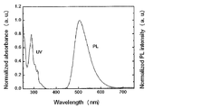
- 2 is an emission spectrum of the organic photoluminescence device of Example 1.
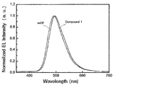
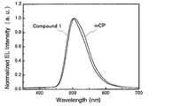
- 2 is an emission spectrum of organic electroluminescence elements of Example 2 and Comparative Example 1.
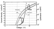
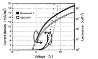
- 6 is a graph showing current density-voltage-luminance characteristics of organic electroluminescence elements of Example 2 and Comparative Example 1.
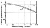
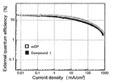
- 6 is a graph showing current density-external quantum efficiency characteristics of organic electroluminescence elements of Example 2 and Comparative Example 1.
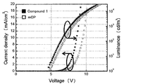
- 6 is a graph showing current density-voltage-luminance characteristics of organic electroluminescence elements of Example 2 and Comparative Example 2.
- 6 is a graph showing current density-external quantum efficiency characteristics of organic electroluminescence elements of Example 2 and Comparative Example 2.
- Example 3 is an emission spectrum of organic electroluminescence elements of Example 3 and Comparative Example 3.
- 6 is a graph showing current density-voltage-luminance characteristics of organic electroluminescence elements of Example 3 and Comparative Example 3.
- 6 is a graph showing current density-external quantum efficiency characteristics of organic electroluminescence elements of Example 3 and Comparative Example 3.
- a numerical range represented by using “to” means a range including numerical values described before and after “to” as a lower limit value and an upper limit value.
- the isotope species of the hydrogen atom present in the molecule of the compound used in the present invention is not particularly limited. For example, all the hydrogen atoms in the molecule may be 1 H, or a part or all of them are 2 H. (Deuterium D) may be used.
- the charge transport material of the present invention is characterized by comprising a compound represented by the following general formula (1).
- R 1 to R 6 are each independently a group represented by the following general formula (2).
- R 7 represents a substituted or unsubstituted aryl group or a substituted or unsubstituted aralkyl group.
- the aromatic ring constituting the aryl group herein may be a single ring or a condensed ring, and specific examples include a benzene ring, a naphthalene ring, an anthracene ring, and a phenanthrene ring.
- the aryl group preferably has 6 to 40 carbon atoms, more preferably 6 to 20 carbon atoms, and still more preferably 6 to 14 carbon atoms.
- aryl group examples include a phenyl group, a 1-naphthyl group, a 2-naphthyl group, a 1-anthracenyl group, a 2-anthracenyl group, and a 9-anthracenyl group.
- the aralkyl group here means an alkyl group substituted with at least one aryl group, and the alkyl part may be linear or branched.
- the alkyl moiety preferably has 1 to 20 carbon atoms, more preferably 1 to 10 carbon atoms, and still more preferably 1 to 5 carbon atoms.
- the aromatic ring constituting the aryl moiety may be a single ring or a condensed ring. For specific examples and preferred carbon numbers, the specific examples and preferred ranges of the above aryl groups can be referred to.
- the aryl group constituting the aralkyl group is preferably bonded to the 1-position of the alkyl group.
- aryl groups constituting the aralkyl group when there are two or more aryl groups constituting the aralkyl group, they may be the same or different from each other.
- Specific examples of the aralkyl group include phenylmethyl group, 1-phenylethyl group, 1-phenylpropyl group, 1-phenylbutyl group, 1-phenylpentyl group, 1-phenylhexyl group, naphthalen-1-ylmethyl group, 1- (Naphthalen-1-yl) ethyl group, naphthalen-2-ylmethyl group, 1- (naphthalen-2-yl) ethyl group can be exemplified.
- R 7 and R 11 may be bonded to each other to form a cyclic structure.
- the formed cyclic structure is preferably a 5- to 7-membered ring, more preferably a 5- or 6-membered ring.
- the formed ring skeleton-forming atom may or may not contain a hetero atom other than the nitrogen atom to which R 7 and R 11 are bonded. When it contains, it can contain a nitrogen atom, a sulfur atom, and an oxygen atom, for example.
- Examples of preferred cyclic structures include 1,4-oxazine ring, 1,4-thiazine ring, pyrazine ring, and pyrrole ring.
- a substituted or unsubstituted alkyl group or a substituted or unsubstituted aryl group is bonded to the nitrogen atom at the 4-position, and a substituted or unsubstituted aryl group is bonded. More preferably, a substituted or unsubstituted phenyl group is more preferably bonded.
- R 11 to R 15 each independently represents a hydrogen atom or a substituent.
- the number of substituents is not particularly limited, and all of R 11 to R 15 may be unsubstituted (that is, hydrogen atoms).
- the plurality of substituents may be the same as or different from each other.
- Examples of the substituent that R 11 to R 15 can take and the substituent that the aryl group or aralkyl group represented by R 7 can take include, for example, a hydroxy group, a halogen atom, a cyano group, an alkyl group having 1 to 20 carbon atoms, and a carbon number of 1
- Heteroaryl group alkenyl group having 2 to 10 carbon atoms, alkynyl group having 2 to 10 carbon atoms, alkoxycarbonyl group having 2 to 10 carbon atoms, alkylsulfonyl group having 1 to 10 carbon atoms, haloalkyl group having 1 to 10 carbon atoms
- substituents are a halogen atom, a cyano group, a substituted or unsubstituted alkyl group having 1 to 20 carbon atoms, an alkoxy group having 1 to 20 carbon atoms, a substituted or unsubstituted aryl group having 6 to 40 carbon atoms, carbon A substituted or unsubstituted heteroaryl group having 3 to 40 carbon atoms, and a dialkyl-substituted amino group having 1 to 20 carbon atoms.
- substituents are a halogen atom, a cyano group, a substituted or unsubstituted alkyl group having 1 to 20 carbon atoms, an alkoxy group having 1 to 20 carbon atoms, a substituted or unsubstituted aryl group having 6 to 40 carbon atoms, carbon A substituted or unsubstituted heteroaryl group having 3 to 40 carbon atoms, and a dialkyl-substituted amino group having 1 to 20 carbon
- substituents are a fluorine atom, a chlorine atom, a cyano group, a substituted or unsubstituted alkyl group having 1 to 10 carbon atoms, a substituted or unsubstituted alkoxy group having 1 to 10 carbon atoms, and a substituted group having 6 to 15 carbon atoms.
- it is an unsubstituted aryl group or a substituted or unsubstituted heteroaryl group having 3 to 12 carbon atoms.
- R 11 and R 12 , R 12 and R 13 , R 13 and R 14 , and R 14 and R 15 may be bonded to each other to form a cyclic structure.
- the cyclic structure may be an aromatic ring or an alicyclic ring, may contain a hetero atom, and the cyclic structure may be a condensed ring of two or more rings.
- the hetero atom here is preferably selected from the group consisting of a nitrogen atom, an oxygen atom and a sulfur atom.
- Examples of cyclic structures formed include benzene ring, naphthalene ring, pyridine ring, pyridazine ring, pyrimidine ring, pyrazine ring, pyrrole ring, imidazole ring, pyrazole ring, triazole ring, imidazoline ring, oxazole ring, isoxazole ring, thiazole And a ring, an isothiazole ring, a cyclohexadiene ring, a cyclohexene ring, a cyclopentaene ring, a cycloheptatriene ring, a cycloheptadiene ring, and a cycloheptaene ring.
- R 1 to R 6 in the general formula (1) may be the same or different. Moreover, a part may be the same. For example, R 1 and R 2 are the same, R 3 and R 4 are the same, R 5 and R 6 are the same, or R 1 , R 3 and R 5 are the same, R 2 and A case where R 4 and R 6 are the same can be mentioned. If all of R 1 to R 6 are the same, there is an advantage that the synthesis is easy.
- R 1 to R 6 in the general formula (1) are preferably groups represented by any of the following general formulas (3) to (7).
- R 21 to R 38 , R 41 to R 48 , R 51 to R 58 , R 61 to R 65 , R 71 to R 79 are each independently a hydrogen atom or a substituent. Represents. For the explanation and preferred ranges of the substituents mentioned here, the explanations and preferred ranges of the substituents which can be taken by the above R 11 to R 15 can be referred.
- the number of substituents in the general formulas (3) to (7) is not particularly limited. It is also preferred that all are unsubstituted (ie hydrogen atoms). Further, when there are two or more substituents in each of the general formulas (3) to (7), these substituents may be the same or different.
- the substituent is preferably any one of R 22 to R 24 and R 27 to R 29 in the case of the general formula (3).
- any one of R 32 to R 37 is preferred, and in general formula (5), any one of R 42 to R 47 is preferred, and general formula (6) R 52 , R 53 , R 56 , R 57 , R 62 to R 64 are preferable, and any one of R 72 to R 74 , R 77 , R 78 is preferable for the general formula (7). It is preferable that
- All of R 1 to R 6 in the general formula (1) are preferably groups represented by any one of the general formulas (3) to (7).
- the case where all of R 1 to R 6 are groups represented by the general formula (3) can be preferably exemplified. At this time, all of R 1 to R 6 may be the same group or different groups.
- R 1 to R 6 in the general formula (1) are preferably groups represented by the following general formula (8).
- the general formula (8) is a structure in which R 25 and R 26 in the general formula (3) are bonded to each other by a single bond.
- R 21 to R 24 and R 27 to R 30 each independently represent a hydrogen atom or a substituent.
- R 21 and R 22 , R 22 and R 23 , R 23 and R 24 , R 27 and R 28 , R 28 and R 29 , and R 29 and R 30 may be bonded to each other to form a cyclic structure.
- the substituent and the explanation of the cyclic structure the corresponding descriptions in the general formula (2) and the general formula (3) can be referred to.
- Preferable examples of the compound represented by the general formula (1) include compounds having the following structure.
- a hydrogen atom present in the following structure may be substituted with a substituent.
- the corresponding descriptions in general formula (2) and general formula (3) can be referred to.
- the molecular weight of the compound represented by the general formula (1) is, for example, 1500 or less when the organic layer containing the compound represented by the general formula (1) is intended to be formed by vapor deposition. Preferably, it is preferably 1200 or less, more preferably 1000 or less, and even more preferably 800 or less.
- the lower limit of the molecular weight is the molecular weight of the minimum compound represented by the general formula (1).
- the compound represented by the general formula (1) may be formed by a coating method regardless of the molecular weight. If a coating method is used, a film can be formed even with a compound having a relatively large molecular weight.
- a compound containing a plurality of structures represented by the general formula (1) in the molecule as a light emitting material.
- a polymer obtained by previously polymerizing a polymerizable group in the structure represented by the general formula (1) and polymerizing the polymerizable group as a light emitting material.
- a monomer containing a polymerizable functional group in any of R 1 to R 6 in the general formula (1) and polymerizing it alone or copolymerizing with other monomers, It is conceivable to obtain a polymer having a repeating unit and use the polymer as a light emitting material.
- it is also possible to obtain a dimer or trimer by coupling compounds having a structure represented by the general formula (1) and use them as a light emitting material.
- Examples of the polymer having a repeating unit containing a structure represented by the general formula (1) include a polymer containing a structure represented by the following general formula (9) or (10).
- Q represents a group including the structure represented by the general formula (1)
- L 1 and L 2 represent a linking group.
- the linking group preferably has 0 to 20 carbon atoms, more preferably 1 to 15 carbon atoms, and still more preferably 2 to 10 carbon atoms. And preferably has a structure represented by - linking group -X 11 -L 11.
- X 11 represents an oxygen atom or a sulfur atom, and is preferably an oxygen atom.
- L 11 represents a linking group, preferably a substituted or unsubstituted alkylene group, or a substituted or unsubstituted arylene group, and a substituted or unsubstituted alkylene group having 1 to 10 carbon atoms, or a substituted or unsubstituted group A phenylene group is more preferable.
- R 101 , R 102 , R 103 and R 104 each independently represent a substituent.
- it is a substituted or unsubstituted alkyl group having 1 to 6 carbon atoms, a substituted or unsubstituted alkoxy group having 1 to 6 carbon atoms, or a halogen atom, more preferably an unsubstituted alkyl group having 1 to 3 carbon atoms.
- An unsubstituted alkoxy group having 1 to 3 carbon atoms, a fluorine atom, and a chlorine atom and more preferably an unsubstituted alkyl group having 1 to 3 carbon atoms and an unsubstituted alkoxy group having 1 to 3 carbon atoms.
- the linking group represented by L 1 and L 2 is any one of R 1 to R 6 having the structure of the general formula (1) constituting Q, R 7 and R 11 to R 15 having the structure of the general formula (2). Any one of R 21 to R 30 of the structure of the general formula (3), any of R 31 to R 38 of the structure of the general formula (4), R 41 to R of the structure of the general formula (5) Any one of 48 , R 51 to R 58 and R 61 to R 65 of the structure of the general formula (6), and R 71 to R 78 of the structure of the general formula (7) can be bonded. .
- Two or more linking groups may be linked to one Q to form a crosslinked structure or a network structure.
- repeating unit examples include structures represented by the following formulas (11) to (14).
- a hydroxy group is introduced into any one of R 1 to R 6 of the structure of the general formula (1), and this is used as a linker as described below. It can be synthesized by reacting a compound to introduce a polymerizable group and polymerizing the polymerizable group.
- the polymer containing a structure represented by the general formula (1) in the molecule may be a polymer consisting only of a repeating unit having the structure represented by the general formula (1), or other structures may be used. It may be a polymer containing repeating units.
- the repeating unit having a structure represented by the general formula (1) contained in the polymer may be a single type or two or more types. Examples of the repeating unit not having the structure represented by the general formula (1) include those derived from monomers used in ordinary copolymerization. Examples thereof include a repeating unit derived from a monomer having an ethylenically unsaturated bond such as ethylene and styrene.
- R in the above formula is the same as the definition of R 1 to R 6 in the general formula (1).
- the above scheme shows a method for synthesizing compounds in which R 1 to R 6 are all the same.
- X represents a halogen atom, and examples thereof include a fluorine atom, a chlorine atom, a bromine atom, and an iodine atom, and a chlorine atom and a bromine atom are preferable.
- the reaction in the above scheme is an application of a known coupling reaction, and known reaction conditions can be appropriately selected and used. For example, it can be synthesized by using NaH in DMF.
- the compound represented by the general formula (1) can also be synthesized by combining other known synthesis reactions.
- the compound represented by the general formula (1) is useful as a charge transport material. In particular, it is useful as a host material in consideration of use in combination with a light-emitting material that is a dopant.
- a thin film containing both the compound represented by the general formula (1) and a light emitting material can realize high light emission efficiency and luminance.
- the compound represented by the general formula (1) is particularly preferable in that it can realize high blue light emission efficiency and luminance when used in combination with a blue light emitting material. In order to realize high luminous efficiency and luminance in combination with such a blue light emitting material, it is necessary that the T1 level is high and the band gap is large.
- the thermal decomposition temperature of the compound represented by the general formula (1) is preferably 330 ° C. or higher, more preferably 350 ° C. or higher, and further preferably 380 ° C. or higher.
- the thermal decomposition temperature here is a temperature at which a weight loss of 5% by weight or more is observed when the compound is heated.
- the compound represented by the general formula (1) Since the compound represented by the general formula (1) has high thermal stability, it has an advantage of high applicability to a thin film formation and an organic light emitting device manufacturing process.
- the compound represented by the general formula (1) can be made relatively low in molecular weight, and therefore has suitability for production because it is easily sublimated.
- hexaphenylcyclotriphosphazene substituted with six carbazol-9-yl groups as described in Patent Document 1 Japanese Patent Application Laid-Open No. 2011-525047
- Patent Document 1 Japanese Patent Application Laid-Open No. 2011-525047
- the compound represented by the general formula (1) has the above-mentioned characteristics and also has a characteristic that high luminous efficiency and luminance can be realized when a thin film is formed together with a light-emitting material.
- the compound represented by the general formula (1) has a sufficiently deep HOMO energy level.
- the energy level of HOMO is clearly deeper than that of hexaphenylcyclotriphosphazene substituted with the above six carbazol-9-yl groups.
- the band gap represented by the general formula (1) is relatively large and is extremely effective as a host material for the blue light-emitting material.
- the band gap of the compound represented by the general formula (1) is preferably 3.0 eV or more, more preferably 3.5 eV or more, and further preferably 3.8 eV or more.
- the light emitting material used in combination with the compound represented by the general formula (1) may be a phosphorescent light emitting material, a fluorescent light emitting material, or a material that emits delayed fluorescence. Good. In particular, when combined with a light emitting material that emits delayed fluorescence (delayed phosphor), it is possible to dramatically increase the light emission efficiency and the luminance. The principle will be described below by taking an organic electroluminescence element as an example.
- the organic electroluminescence element carriers are injected into the light emitting material from both positive and negative electrodes to generate an excited light emitting material and emit light.
- 25% of the generated excitons are excited to the excited singlet state, and the remaining 75% are excited to the excited triplet state. Therefore, the use efficiency of energy is higher when phosphorescence, which is light emission from an excited triplet state, is used.
- the excited triplet state has a long lifetime, energy saturation occurs due to saturation of the excited state and interaction with excitons in the excited triplet state, and in general, the quantum yield of phosphorescence is often not high.
- delayed fluorescent materials after energy transition to an excited triplet state due to intersystem crossing, etc., are then crossed back to an excited singlet state due to triplet-triplet annihilation or absorption of thermal energy, and emit fluorescence.
- a thermally activated delayed fluorescent material by absorption of thermal energy is particularly useful.
- excitons in the excited singlet state emit fluorescence as usual.
- excitons in the excited triplet state absorb heat generated by the device and cross between the excited singlets to emit fluorescence.
- the light is emitted from the excited singlet, the light is emitted at the same wavelength as the fluorescence, but the light lifetime (luminescence lifetime) generated by the reverse intersystem crossing from the excited triplet state to the excited singlet state is normal. Since the fluorescence becomes longer than the fluorescence and phosphorescence, it is observed as fluorescence delayed from these. This can be defined as delayed fluorescence. If such a heat-activated exciton transfer mechanism is used, the ratio of the compound in an excited singlet state, which normally generated only 25%, is increased to 25% or more by absorbing thermal energy after carrier injection. It can be raised.
- the heat of the device will sufficiently cause intersystem crossing from the excited triplet state to the excited singlet state and emit delayed fluorescence. Efficiency can be improved dramatically.
- the light emitting material that can be used in combination with the compound represented by the general formula (1) is preferably a blue light emitting material, but a light emitting material that emits light of other colors may be used in combination.
- Conventionally known materials can be used as the blue light emitting material. Examples thereof include coumarin, perylene, pyrene, anthracene, p-bis (2-phenylethenyl) benzene, and derivatives thereof.
- specific light emitting materials that can be used in combination with the compound represented by the general formula (1) the following compounds can be preferably exemplified.
- Organic light emitting device By using the compound represented by the general formula (1) of the present invention as a charge transporting material or a host material of a light emitting layer, an excellent organic photoluminescence element (organic PL element), organic electroluminescence element (organic EL element), etc. An organic light emitting device can be provided. At this time, the compound represented by the general formula (1) of the present invention may have a function of assisting light emission of another light emitting material included in the light emitting layer as a so-called assist dopant.
- the compound represented by the general formula (1) of the present invention contained in the light emitting layer includes the lowest excitation singlet energy level of the host material contained in the light emitting layer and the lowest excitation of other light emitting materials contained in the light emitting layer. It may have the lowest excited singlet energy level between singlet energy levels.
- the organic photoluminescence element has a structure in which at least a light emitting layer is formed on a substrate.
- the organic electroluminescence element has a structure in which an organic layer is formed at least between an anode, a cathode, and an anode and a cathode.
- the organic layer includes at least a light emitting layer, and may consist of only the light emitting layer, or may have one or more organic layers in addition to the light emitting layer.
- Examples of such other organic layers include a hole transport layer, a hole injection layer, an electron blocking layer, a hole blocking layer, an electron injection layer, an electron transport layer, and an exciton blocking layer.
- the hole transport layer may be a hole injection / transport layer having a hole injection function
- the electron transport layer may be an electron injection / transport layer having an electron injection function.
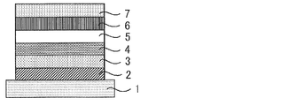
- FIG. 1 A specific example of the structure of an organic electroluminescence element is shown in FIG. In FIG. 1, 1 is a substrate, 2 is an anode, 3 is a hole injection layer, 4 is a hole transport layer, 5 is a light emitting layer, 6 is an electron transport layer, and 7 is a cathode. Below, each member and each layer of an organic electroluminescent element are demonstrated. In addition, description of a board
- the organic electroluminescence device of the present invention is preferably supported on a substrate.
- the substrate is not particularly limited and may be any substrate conventionally used for organic electroluminescence elements.
- a substrate made of glass, transparent plastic, quartz, silicon, or the like can be used.
- an electrode material made of a metal, an alloy, an electrically conductive compound, or a mixture thereof having a high work function (4 eV or more) is preferably used.
- electrode materials include metals such as Au, and conductive transparent materials such as CuI, indium tin oxide (ITO), SnO 2 , and ZnO.
- conductive transparent materials such as CuI, indium tin oxide (ITO), SnO 2 , and ZnO.
- an amorphous material such as IDIXO (In 2 O 3 —ZnO) that can form a transparent conductive film may be used.
- a thin film may be formed by vapor deposition or sputtering of these electrode materials, and a pattern of a desired shape may be formed by photolithography, or when pattern accuracy is not so high (about 100 ⁇ m or more) ), A pattern may be formed through a mask having a desired shape at the time of vapor deposition or sputtering of the electrode material.
- wet film-forming methods such as a printing system and a coating system, can also be used.
- the transmittance be greater than 10%, and the sheet resistance as the anode is preferably several hundred ⁇ / ⁇ or less.
- the film thickness depends on the material, it is usually selected in the range of 10 to 1000 nm, preferably 10 to 200 nm.
- cathode a material having a low work function (4 eV or less) metal (referred to as an electron injecting metal), an alloy, an electrically conductive compound, and a mixture thereof as an electrode material is used.
- electrode materials include sodium, sodium-potassium alloy, magnesium, lithium, magnesium / copper mixture, magnesium / silver mixture, magnesium / aluminum mixture, magnesium / indium mixture, aluminum / aluminum oxide (Al 2 O 3 ) Mixtures, indium, lithium / aluminum mixtures, rare earth metals and the like.
- a mixture of an electron injecting metal and a second metal which is a stable metal having a larger work function value than this for example, a magnesium / silver mixture
- Suitable are a magnesium / aluminum mixture, a magnesium / indium mixture, an aluminum / aluminum oxide (Al 2 O 3 ) mixture, a lithium / aluminum mixture, aluminum and the like.
- the cathode can be produced by forming a thin film of these electrode materials by a method such as vapor deposition or sputtering.
- the sheet resistance as the cathode is preferably several hundred ⁇ / ⁇ or less, and the film thickness is usually selected in the range of 10 nm to 5 ⁇ m, preferably 50 to 200 nm.
- the emission luminance is advantageously improved.
- a transparent or semi-transparent cathode can be produced. By applying this, an element in which both the anode and the cathode are transparent is used. Can be produced.
- the light emitting layer is a layer that emits light after excitons are generated by recombination of holes and electrons injected from each of the anode and the cathode, and the light emitting material may be used alone for the light emitting layer. , Preferably including a luminescent material and a host material. As a host material, 1 type (s) or 2 or more types selected from the compound group represented by General formula (1) can be used. In order for the organic electroluminescent device and the organic photoluminescent device of the present invention to exhibit high luminous efficiency, it is important to confine singlet excitons and triplet excitons generated in the light emitting material in the light emitting material.
- a host material represented by the general formula (1) in addition to the light emitting material in the light emitting layer.
- the host material an organic compound in which at least one of excited singlet energy and excited triplet energy has a value higher than that of the light-emitting material can be used.
- singlet excitons and triplet excitons generated in the light emitting material can be confined in the molecule of the light emitting material, and the light emission efficiency can be sufficiently extracted.
- singlet excitons and triplet excitons cannot be sufficiently confined, there are cases where high luminous efficiency can be obtained, so that host materials that can achieve high luminous efficiency are particularly limited. And can be used in the present invention.
- light emission is generated from the light-emitting material contained in the light-emitting layer.
- This luminescence may be any of phosphorescence, fluorescence, and delayed fluorescence, and may include a plurality of these.
- light emission from the host material may be partly or partly emitted.
- the amount of the light emitting material contained in the light emitting layer is preferably 0.1% by weight or more, more preferably 1% by weight or more, and 50% by weight or less. It is preferably 20% by weight or less, more preferably 10% by weight or less.
- the host material in the light-emitting layer is preferably an organic compound that has a hole transporting ability and an electron transporting ability, prevents the emission of longer wavelengths, and has a high glass transition temperature.
- the injection layer is a layer provided between the electrode and the organic layer for lowering the driving voltage and improving the luminance of light emission.
- the injection layer can be provided as necessary.
- the blocking layer is a layer that can prevent diffusion of charges (electrons or holes) and / or excitons existing in the light emitting layer to the outside of the light emitting layer.
- the electron blocking layer can be disposed between the light emitting layer and the hole transport layer and blocks electrons from passing through the light emitting layer toward the hole transport layer.
- a hole blocking layer can be disposed between the light emitting layer and the electron transporting layer to prevent holes from passing through the light emitting layer toward the electron transporting layer.
- the blocking layer can also be used to block excitons from diffusing outside the light emitting layer. That is, each of the electron blocking layer and the hole blocking layer can also function as an exciton blocking layer.
- the term “electron blocking layer” or “exciton blocking layer” as used herein is used in the sense of including a layer having the functions of an electron blocking layer and an exciton blocking layer in one layer.
- the hole blocking layer has a function of an electron transport layer in a broad sense.
- the hole blocking layer has a role of blocking holes from reaching the electron transport layer while transporting electrons, thereby improving the recombination probability of electrons and holes in the light emitting layer.
- the material for the hole blocking layer the material for the electron transport layer described later can be used as necessary.
- the electron blocking layer has a function of transporting holes in a broad sense.
- the electron blocking layer has a role to block electrons from reaching the hole transport layer while transporting holes, thereby improving the probability of recombination of electrons and holes in the light emitting layer. .
- the exciton blocking layer is a layer for preventing excitons generated by recombination of holes and electrons in the light emitting layer from diffusing into the charge transport layer. It becomes possible to efficiently confine in the light emitting layer, and the light emission efficiency of the device can be improved.
- the exciton blocking layer can be inserted on either the anode side or the cathode side adjacent to the light emitting layer, or both can be inserted simultaneously.
- the layer when the exciton blocking layer is provided on the anode side, the layer can be inserted adjacent to the light emitting layer between the hole transport layer and the light emitting layer, and when inserted on the cathode side, the light emitting layer and the cathode Between the luminescent layer and the light-emitting layer.
- a hole injection layer, an electron blocking layer, or the like can be provided between the anode and the exciton blocking layer adjacent to the anode side of the light emitting layer, and the excitation adjacent to the cathode and the cathode side of the light emitting layer can be provided.
- an electron injection layer, an electron transport layer, a hole blocking layer, and the like can be provided.
- the blocking layer is disposed, at least one of the excited singlet energy and the excited triplet energy of the material used as the blocking layer is preferably higher than the excited singlet energy and the excited triplet energy of the light emitting material.
- the hole transport layer is made of a hole transport material having a function of transporting holes, and the hole transport layer can be provided as a single layer or a plurality of layers.
- the hole transport material has any one of hole injection or transport and electron barrier properties, and may be either organic or inorganic.
- hole transport materials that can be used include, for example, triazole derivatives, oxadiazole derivatives, imidazole derivatives, carbazole derivatives, indolocarbazole derivatives, polyarylalkane derivatives, pyrazoline derivatives and pyrazolone derivatives, phenylenediamine derivatives, arylamine derivatives, Examples include amino-substituted chalcone derivatives, oxazole derivatives, styrylanthracene derivatives, fluorenone derivatives, hydrazone derivatives, stilbene derivatives, silazane derivatives, aniline copolymers, and conductive polymer oligomers, particularly thiophene oligomers.
- An aromatic tertiary amine compound and an styrylamine compound are preferably used, and an aromatic tertiary amine compound is more preferably used.
- the electron transport layer is made of a material having a function of transporting electrons, and the electron transport layer can be provided as a single layer or a plurality of layers.
- the electron transport material (which may also serve as a hole blocking material) may have a function of transmitting electrons injected from the cathode to the light emitting layer.
- Examples of the electron transport layer that can be used include nitro-substituted fluorene derivatives, diphenylquinone derivatives, thiopyran dioxide oxide derivatives, carbodiimides, fluorenylidenemethane derivatives, anthraquinodimethane and anthrone derivatives, oxadiazole derivatives, and the like.
- a thiadiazole derivative in which the oxygen atom of the oxadiazole ring is substituted with a sulfur atom, and a quinoxaline derivative having a quinoxaline ring known as an electron withdrawing group can also be used as an electron transport material.
- a polymer material in which these materials are introduced into a polymer chain or these materials are used as a polymer main chain can also be used.
- the compound represented by the general formula (1) may be used as a host material for the light emitting layer, or may be used as a charge transport material for other organic layers.
- the compound represented by General formula (1) used for a light emitting layer and the compound represented by General formula (1) used for layers other than a light emitting layer may be same or different.
- the compound represented by the general formula (1) may be used for the injection layer, blocking layer, hole blocking layer, electron blocking layer, exciton blocking layer, hole transporting layer, electron transporting layer, and the like. .
- the method for forming these layers is not particularly limited, and the layer may be formed by either a dry process or a wet process.
- the preferable material which can be used for an organic electroluminescent element is illustrated concretely.
- the material that can be used in the present invention is not limited to the following exemplary compounds. Moreover, even if it is a compound illustrated as a material which has a specific function, it can also be diverted as a material which has another function.
- R and R 2 to R 7 each independently represent a hydrogen atom or a substituent.
- n represents an integer of 3 to 5.
- the organic electroluminescence device produced by the above-described method emits light by applying an electric field between the anode and the cathode of the obtained device. At this time, if the light is emitted by excited singlet energy, light having a wavelength corresponding to the energy level is confirmed as fluorescence emission and delayed fluorescence emission. In addition, in the case of light emission by excited triplet energy, a wavelength corresponding to the energy level is confirmed as phosphorescence. Since normal fluorescence has a shorter fluorescence lifetime than delayed fluorescence, the emission lifetime can be distinguished from fluorescence and delayed fluorescence.
- the excited triplet energy is unstable and is converted into heat and the like, and the lifetime is short and it is immediately deactivated.
- the excited triplet energy of a normal organic compound it can be measured by observing light emission under extremely low temperature conditions.
- the organic electroluminescence element of the present invention can be applied to any of a single element, an element having a structure arranged in an array, and a structure in which an anode and a cathode are arranged in an XY matrix.
- an organic light emitting device with greatly improved light emission efficiency can be obtained by containing the compound represented by the general formula (1) in the light emitting layer.
- the organic light emitting device such as the organic electroluminescence device of the present invention can be further applied to various uses. For example, it is possible to produce an organic electroluminescence display device using the organic electroluminescence element of the present invention. For details, see “Organic EL Display” (Ohm Co., Ltd.) ) Can be referred to.
- the organic electroluminescence device of the present invention can be applied to organic electroluminescence illumination and backlights that are in great demand.
- Test Example 2 Measurement of T1 Level
- a methylene chloride solution of compound 1 (concentration 10 ⁇ 4 mol / L) was cooled to 77 ° K, and a PL spectrum was measured. The energy of the peak value on the shortest wavelength side of the PL spectrum was calculated and used as the T1 level (lowest excited triplet energy level) of the compound.
- the T1 level of Compound 1 was 3.00 eV (HOMO: 6.48 eV, LUMO: 2.52 eV).
- Appl. Phys. Lett., 2003, 82, 2422 reported that the T1 level of mCP is 2.9 eV (HOMO: 5.9 eV, LUMO: 2.4 eV).
- Example 1 Fabrication and evaluation of organic photoluminescence devices (thin films) (Example 1) A thin film having a concentration of 2CzCN of 3.0 wt% is obtained by depositing Compound 1 and 2CzCN from different deposition sources on a silicon substrate by a vacuum deposition method under a vacuum degree of 5.0 ⁇ 10 ⁇ 4 Pa. An organic photoluminescence device was formed at a thickness of 100 nm at 0.3 nm / second.
- FIG. 2 shows the result of measuring the emission spectrum of the produced organic photoluminescence device using ultraviolet excitation light. The photoluminescence quantum efficiency was 66.0% under the atmosphere and 84.8% under the nitrogen atmosphere.
- Example 2 Preparation and evaluation of organic electroluminescence device (Example 2) Each thin film was laminated at a vacuum degree of 5.0 ⁇ 10 ⁇ 4 Pa by a vacuum deposition method on a glass substrate on which an anode made of indium tin oxide (ITO) having a thickness of 100 nm was formed. First, ⁇ -NPD was formed on ITO to a thickness of 35 nm, and mCP was formed thereon to a thickness of 10 nm. Next, Compound 1 and 2CzCN were co-evaporated from different vapor deposition sources to form a 20 nm thick layer as a light emitting layer. At this time, the concentration of 2CzCN was set to 3.0% by weight.
- ITO indium tin oxide
- PPT was formed to a thickness of 40 nm
- LiF was further vacuum-deposited to 0.8 nm
- aluminum (Al) was evaporated to a thickness of 80 nm to form a cathode, whereby an organic electroluminescent element was obtained.
- the emission spectrum of the produced organic electroluminescence element is shown in FIG. 3, the current density-voltage-luminance characteristics are shown in FIG. 4, and the current density-external quantum efficiency characteristics are shown in FIG.
- the maximum luminance was 18805 cd / m 2 and the external quantum efficiency was very high at 14.9%.
- Example 1 An organic electroluminescence device was prepared in the same manner as in Example 2 using mCP instead of Compound 1, and the characteristics were evaluated in the same manner.
- the emission spectrum is shown in FIG. 3, the current density-voltage-luminance characteristic is shown in FIG. 4, and the current density-external quantum efficiency characteristic is shown in FIG.
- the maximum luminance was 16524 cd / m 2 and the external quantum efficiency was 11.8%. It was confirmed that the use of Compound 1 over mCP can provide an excellent organic electroluminescence device.
- Example 2 An organic electroluminescence device was prepared in the same manner as in Example 2 using tBuCzPO instead of Compound 1, and the characteristics were evaluated in the same manner.
- FIG. 6 shows current density-voltage-luminance characteristics
- FIG. 7 shows current density-external quantum efficiency characteristics. The maximum luminance was 6436 cd / m 2 and the external quantum efficiency was 12.8%. It was confirmed that the use of Compound 1 over tBuCzPO can provide an excellent organic electroluminescence device.
- Example 3 Each thin film was laminated at a vacuum degree of 5.0 ⁇ 10 ⁇ 4 Pa by a vacuum deposition method on a glass substrate on which an anode made of indium tin oxide (ITO) having a thickness of 100 nm was formed.
- ITO indium tin oxide
- ⁇ -NPD was formed on ITO to a thickness of 35 nm
- mCP was formed thereon to a thickness of 10 nm.
- Compound 1 and 4CzIPN were co-evaporated from different vapor deposition sources to form a 20 nm thick layer as a light emitting layer. At this time, the concentration of 4CzIPN was 3.0% by weight.
- PPT was formed to a thickness of 40 nm
- LiF was further vacuum-deposited to 0.8 nm
- aluminum (Al) was evaporated to a thickness of 80 nm to form a cathode, whereby an organic electroluminescent element was obtained.
- the emission spectrum of the produced organic electroluminescence element is shown in FIG. 8, the current density-voltage-luminance characteristics are shown in FIG. 9, and the current density-external quantum efficiency characteristics are shown in FIG.
- the maximum luminance was 54141 cd / m 2 , and the external quantum efficiency was extremely high at 17.8%.
- Example 3 An organic electroluminescence device was prepared in the same manner as in Example 3 using mCP instead of Compound 1, and the characteristics were evaluated in the same manner.
- the emission spectrum is shown in FIG. 8, the current density-voltage-luminance characteristic is shown in FIG. 9, and the current density-external quantum efficiency characteristic is shown in FIG.
- the maximum luminance was 49176 cd / m 2 and the external quantum efficiency was 17.7%. It was confirmed that the use of Compound 1 over mCP can provide an excellent organic electroluminescence device.
- the compound represented by the general formula (1) is useful as a charge transport material. It is also useful as a host material when a light emitting material is used as a dopant. For this reason, the organic light emitting element using the compound represented by General formula (1) can implement
Landscapes
- Chemical & Material Sciences (AREA)
- Engineering & Computer Science (AREA)
- Materials Engineering (AREA)
- Organic Chemistry (AREA)
- Physics & Mathematics (AREA)
- Spectroscopy & Molecular Physics (AREA)
- Health & Medical Sciences (AREA)
- Life Sciences & Earth Sciences (AREA)
- Biochemistry (AREA)
- General Health & Medical Sciences (AREA)
- Molecular Biology (AREA)
- Electroluminescent Light Sources (AREA)
Abstract
Description

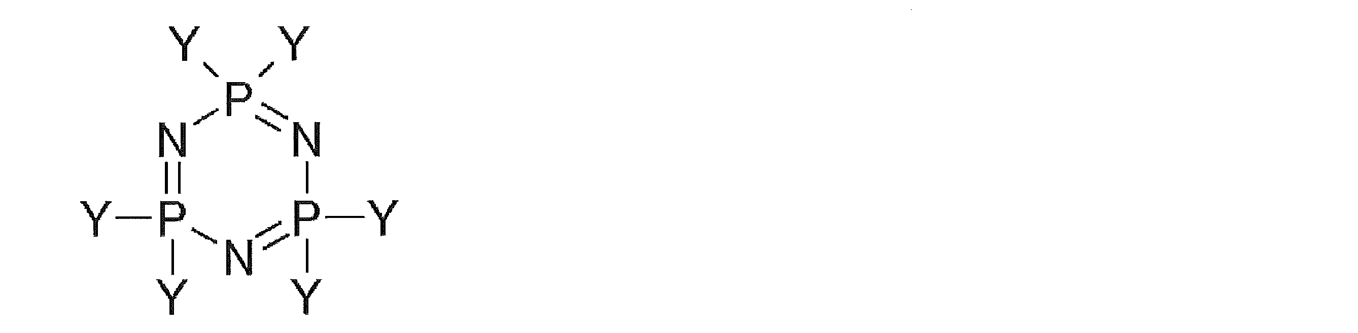
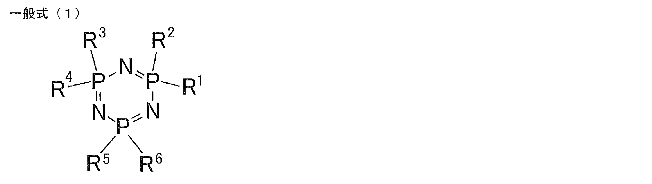
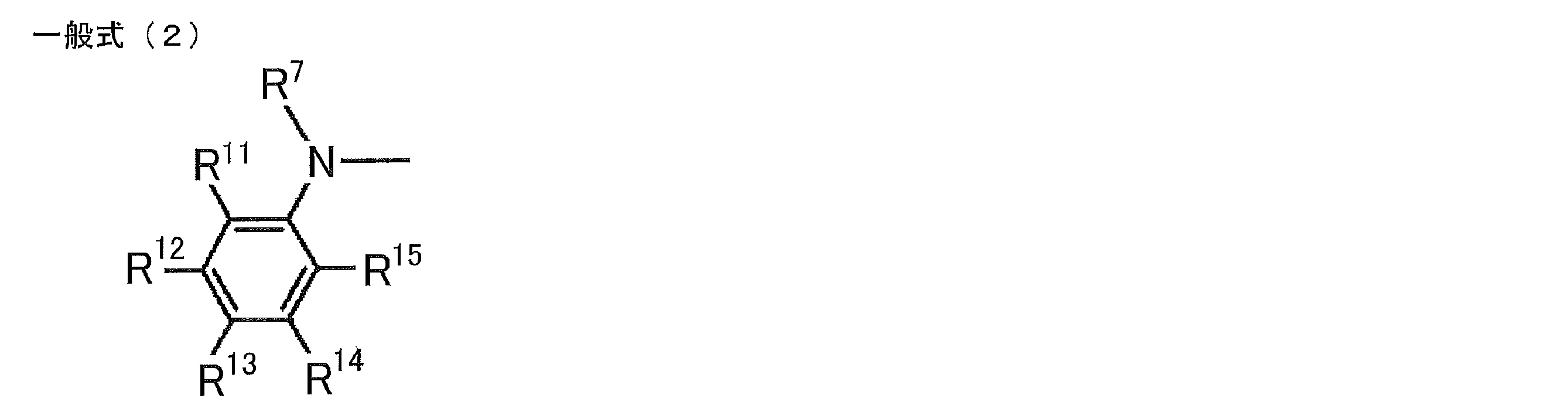
[2] 一般式(1)のR1~R6がすべて同一であることを特徴とする[1]に記載の電荷輸送材料。
[3] 一般式(1)のR1~R6が下記一般式(3)~(7)のいずれかで表される基であることを特徴とする[1]または[2]に記載の電荷輸送材料。

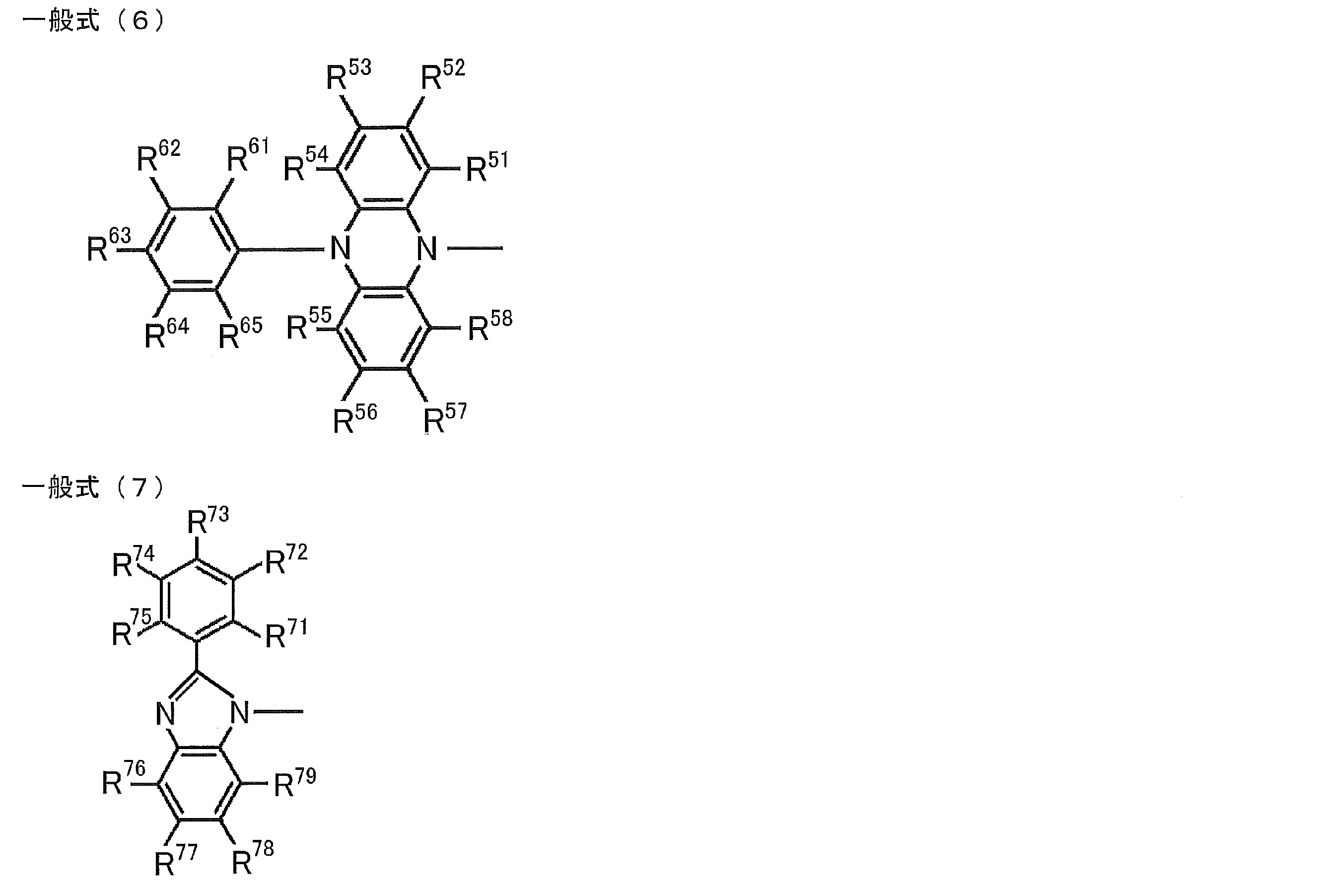
[4] 一般式(1)のR1~R6が前記一般式(3)で表される基であることを特徴とする[3]に記載の電荷輸送材料。
[5] 一般式(1)のR1~R6が下記一般式(8)で表される基であることを特徴とする[3]または[4]に記載の電荷輸送材料。
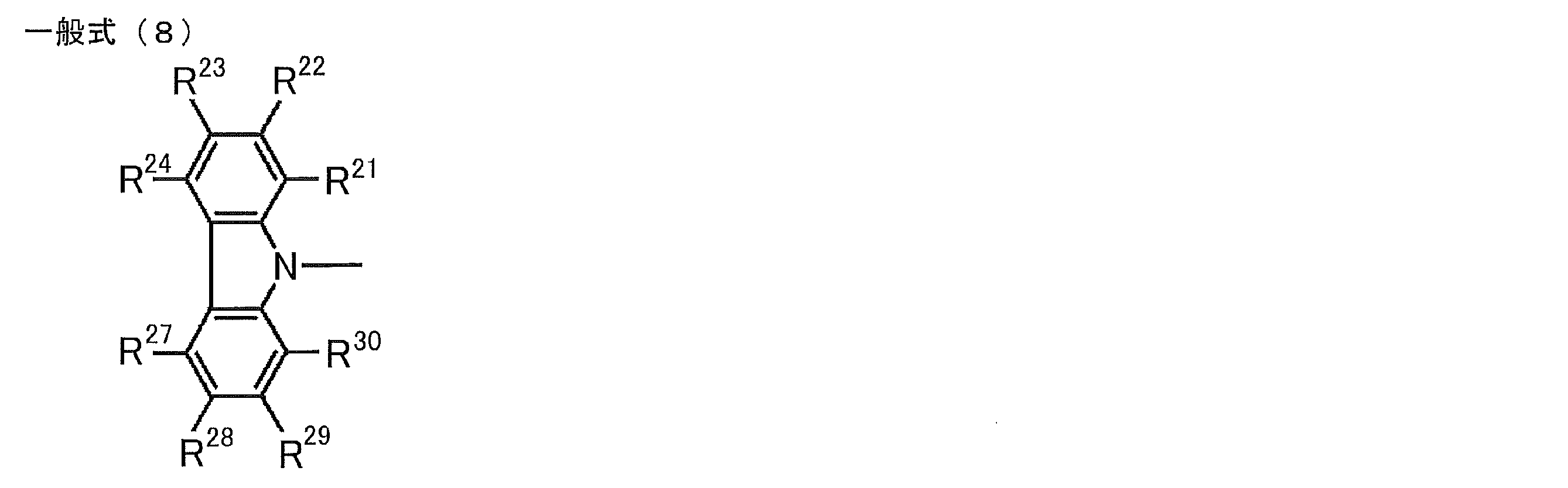
[6] 下記の構造を有する化合物からなることを特徴とする[5]に記載の電荷輸送材料。

[7] [1]~[6]のいずれか1項に記載の電荷輸送材料からなることを特徴とするホスト材料。
[8] 青色発光材料用であることを特徴とする[7]に記載のホスト材料。
[9] [7]に記載のホスト材料と発光材料を含むことを特徴とする薄膜。
[10] 前記発光材料が青色発光材料であることを特徴とする[9]に記載の薄膜。
[11] [1]~[6]のいずれか1項に記載の電荷輸送材料を用いたことを特徴とする有機発光素子。
[12] 前記電荷輸送材料をホスト材料として発光層に用いたことを特徴とする[11]に記載の有機発光素子。
[13] リン光を放射することを特徴とする[11]または[12]に記載の有機発光素子。
[14] 遅延蛍光を放射することを特徴とする[11]または[12]に記載の有機発光素子。
[15] 有機エレクトロルミネッセンス素子であることを特徴とする[11]~[14]のいずれか1項に記載の有機発光素子。
本発明の電荷輸送材料は、下記一般式(1)で表される化合物からなることを特徴とする。
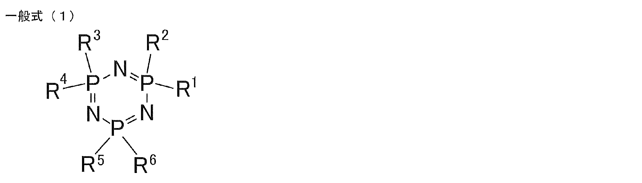
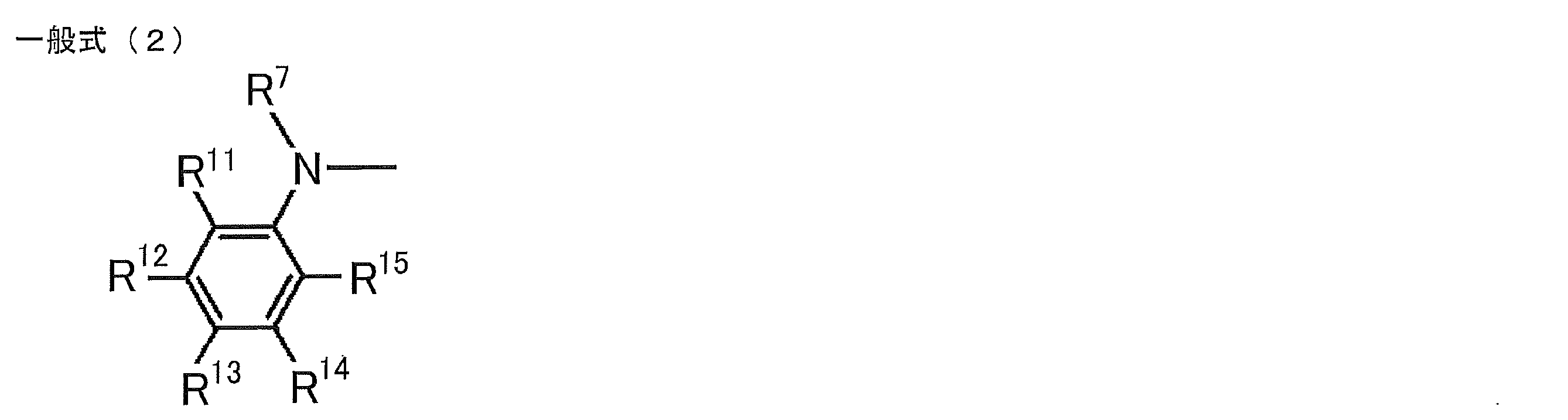
ここでいうアリール基を構成する芳香環は、単環であっても縮合環であってもよく、具体例としてベンゼン環、ナフタレン環、アントラセン環、フェナントレン環を挙げることができる。アリール基の炭素数は6~40であることが好ましく、6~20であることがより好ましく、6~14であることがさらに好ましい。アリール基の具体例として、フェニル基、1-ナフチル基、2-ナフチル基、1-アントラセニル基、2-アントラセニル基、9-アントラセニル基を挙げることができる。
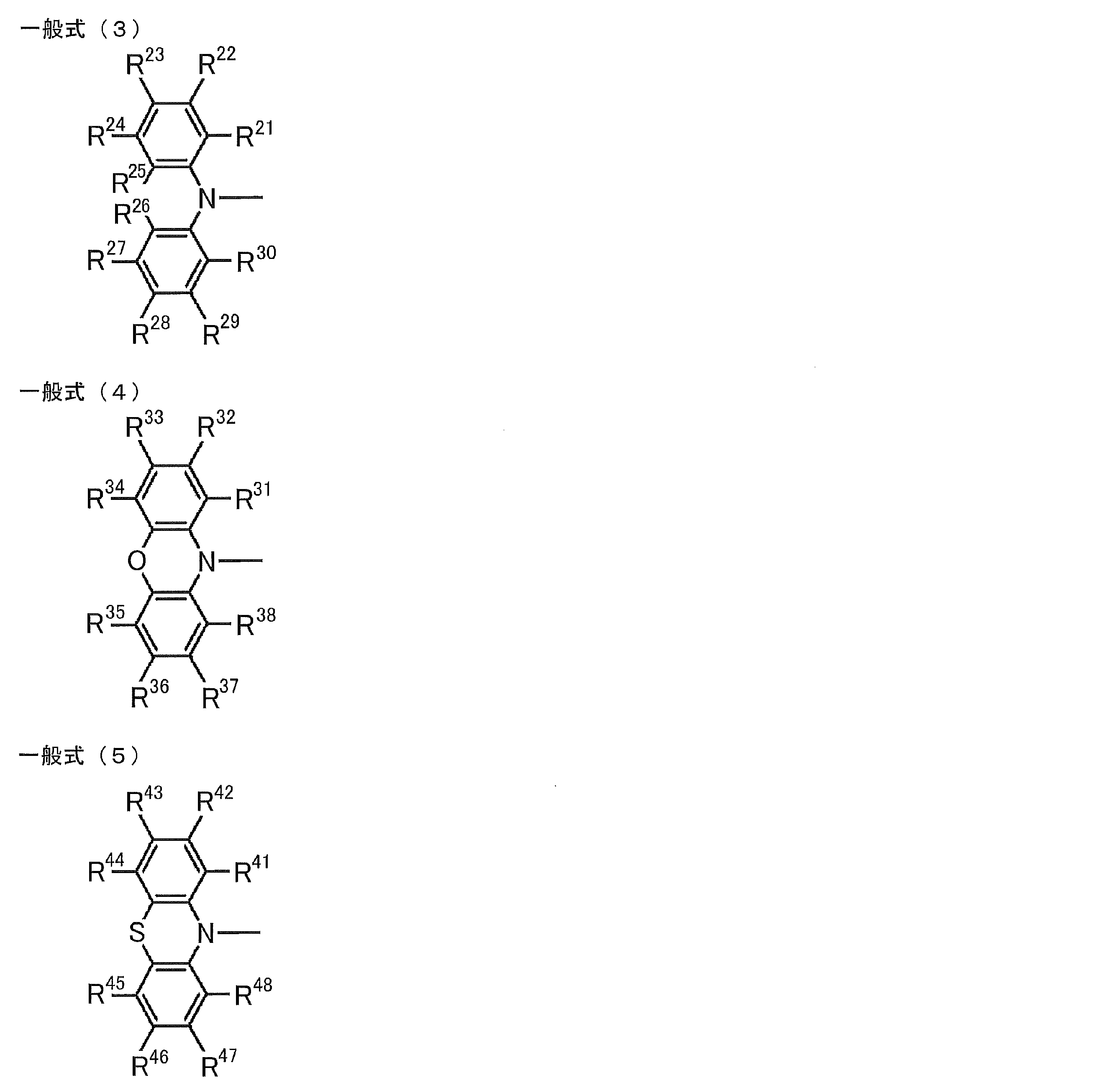

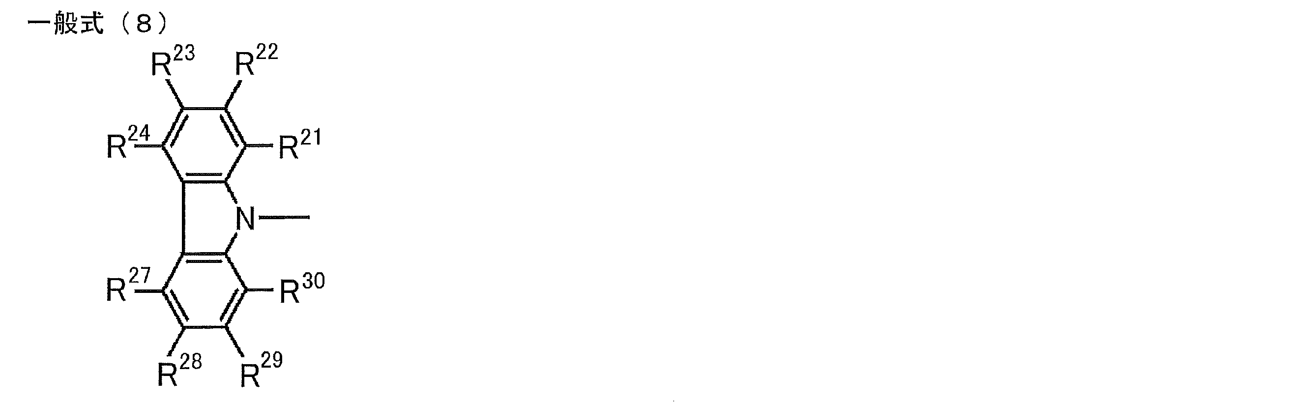
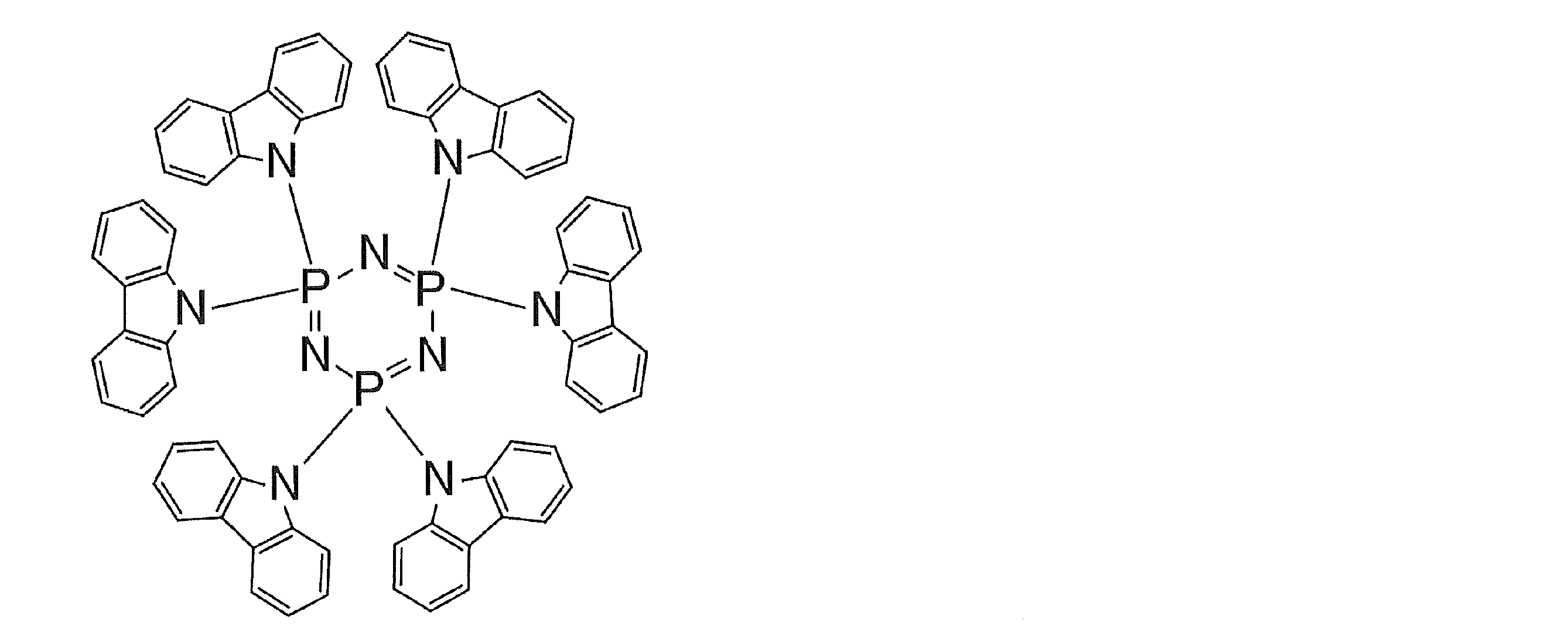

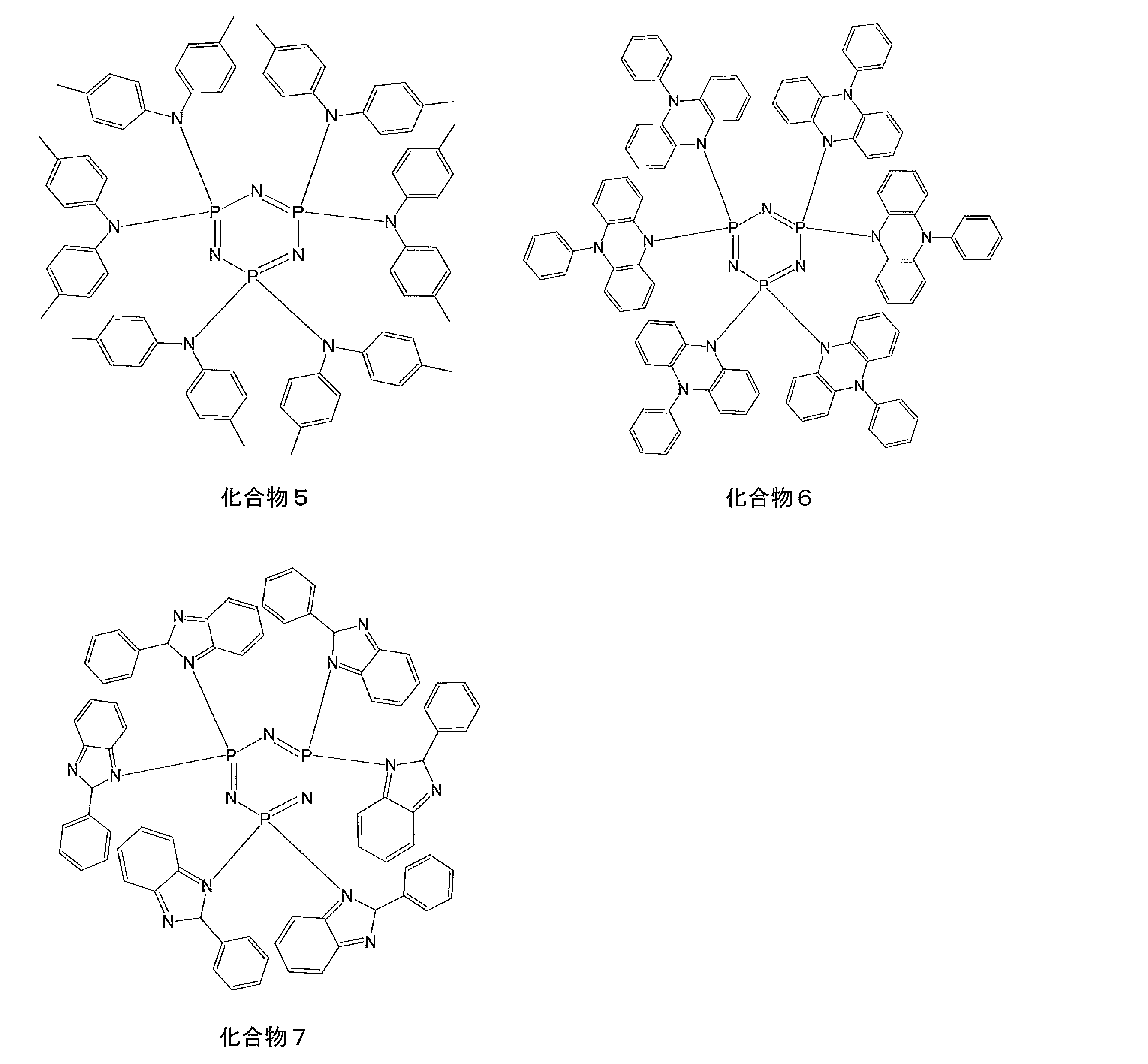
一般式(1)で表される化合物は、分子量にかかわらず塗布法で成膜してもよい。塗布法を用いれば、分子量が比較的大きな化合物であっても成膜することが可能である。
例えば、一般式(1)で表される構造中にあらかじめ重合性基を存在させておいて、その重合性基を重合させることによって得られる重合体を、発光材料として用いることが考えられる。具体的には、一般式(1)のR1~R6のいずれかに重合性官能基を含むモノマーを用意して、これを単独で重合させるか、他のモノマーとともに共重合させることにより、繰り返し単位を有する重合体を得て、その重合体を発光材料として用いることが考えられる。あるいは、一般式(1)で表される構造を有する化合物どうしをカップリングさせることにより、二量体や三量体を得て、それらを発光材料として用いることも考えられる。
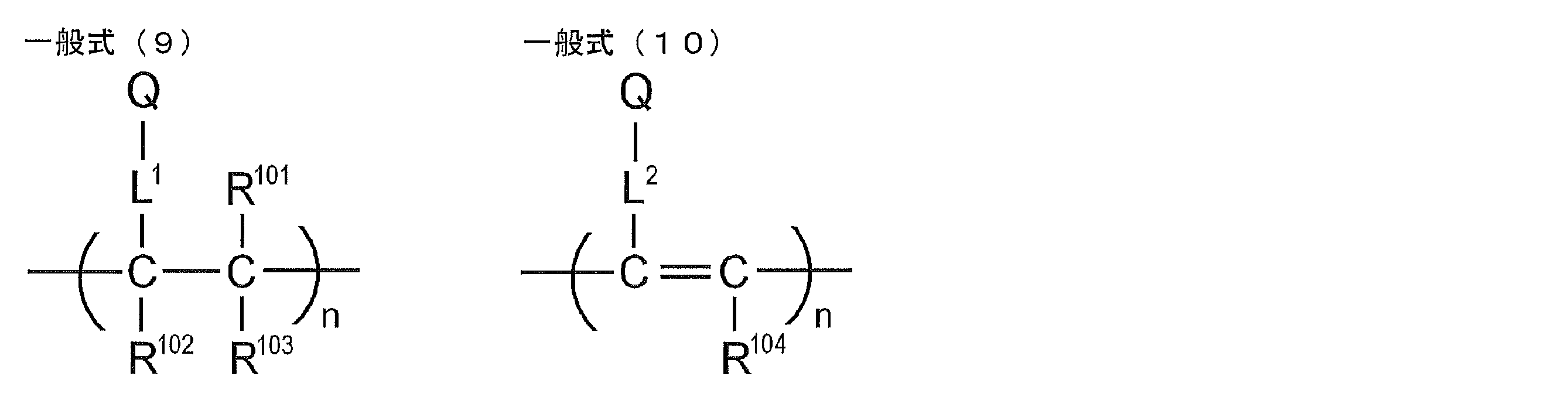
一般式(9)および(10)において、R101、R102、R103およびR104は、各々独立に置換基を表す。好ましくは、炭素数1~6の置換もしくは無置換のアルキル基、炭素数1~6の置換もしくは無置換のアルコキシ基、ハロゲン原子であり、より好ましくは炭素数1~3の無置換のアルキル基、炭素数1~3の無置換のアルコキシ基、フッ素原子、塩素原子であり、さらに好ましくは炭素数1~3の無置換のアルキル基、炭素数1~3の無置換のアルコキシ基である。
L1およびL2で表される連結基は、Qを構成する一般式(1)の構造のR1~R6のいずれか、一般式(2)の構造のR7、R11~R15のいずれか、一般式(3)の構造のR21~R30のいずれか、一般式(4)の構造のR31~R38のいずれか、一般式(5)の構造のR41~R48のいずれか、一般式(6)の構造のR51~R58、R61~R65のいずれか、一般式(7)の構造のR71~R78のいずれかに結合することができる。1つのQに対して連結基が2つ以上連結して架橋構造や網目構造を形成していてもよい。

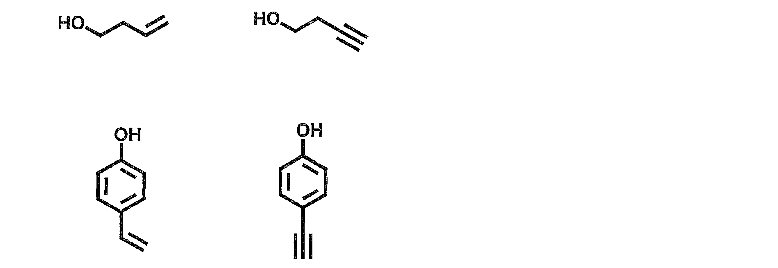
一般式(1)で表される化合物は、既知の反応を組み合わせることによって合成することができる。例えば、以下のスキームにしたがって合成することが可能である。
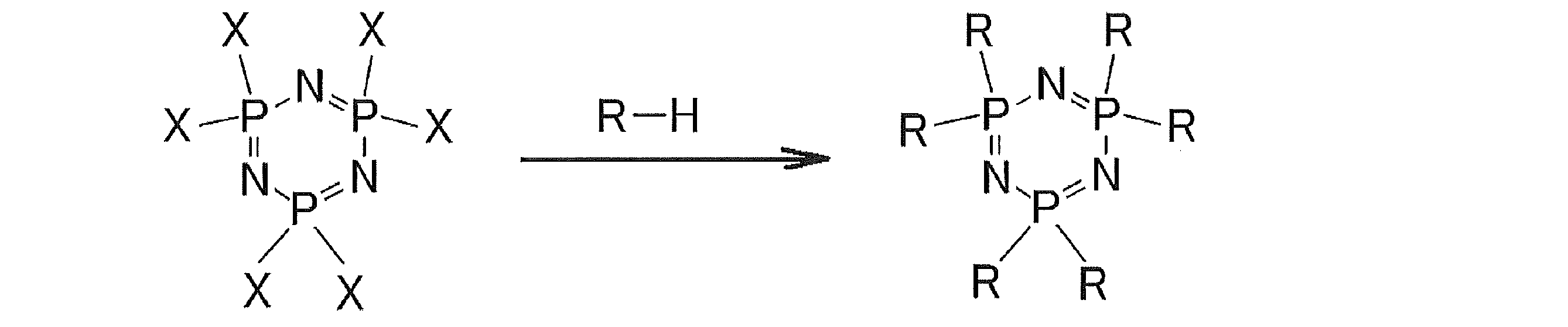
上記のスキームにおける反応は、公知のカップリング反応を応用したものであり、公知の反応条件を適宜選択して用いることができる。例えばDMF中でNaHを用いることにより合成することが可能である。また、一般式(1)で表される化合物は、その他の公知の合成反応を組み合わせることによっても合成することができる。
一般式(1)で表される化合物は、電荷輸送材料として有用である。特に、ドーパントである発光材料と組み合わせて用いることを念頭においたホスト材料として有用である。一般式(1)で表される化合物と発光材料をともに含有する薄膜は、高い発光効率や輝度を実現することができる。一般式(1)で表される化合物は、特に青色発光材料と組み合わせて用いることにより、高い青色発光効率や輝度を実現しうる点で好ましい。このような青色発光材料と組み合わせて高い発光効率や輝度を実現するためには、T1レベルが高くてバンドギャップが大きいことが必要とされる。一般に、T1レベルが高い材料は、熱安定性が悪いという問題がある。上記の非特許文献1(Chem. Mater., 2011, 23 (22), 4947-4953)に記載されるシクロトリホスファゼン化合物も、T1レベルは高いものの、熱安定性は十分に満足が行く程度に高いとは言えなかった。これに対する解決策は従来示されていなかったが、本発明らが提案する一般式(1)で表される化合物は、T1レベルが高いだけでなく、熱安定性も高いという優れた特徴を兼ね備えている。一般式(1)で表される化合物の熱分解温度は、好ましくは330℃以上であり、より好ましくは350℃以上であり、さらに好ましくは380℃以上である。なお、ここでいう熱分解温度は化合物を加熱していったときに5重量%以上の重量減少が認められる温度である。

本発明の一般式(1)で表される化合物を電荷輸送材料または発光層のホスト材料として用いることにより、有機フォトルミネッセンス素子(有機PL素子)や有機エレクトロルミネッセンス素子(有機EL素子)などの優れた有機発光素子を提供することができる。このとき、本発明の一般式(1)で表される化合物は、いわゆるアシストドーパントとして、発光層に含まれる他の発光材料の発光をアシストする機能を有するものであってもよい。すなわち、発光層に含まれる本発明の一般式(1)で表される化合物は、発光層に含まれるホスト材料の最低励起一重項エネルギー準位と発光層に含まれる他の発光材料の最低励起一重項エネルギー準位の間の最低励起一重項エネルギー準位を有するものであってもよい。
有機フォトルミネッセンス素子は、基板上に少なくとも発光層を形成した構造を有する。また、有機エレクトロルミネッセンス素子は、少なくとも陽極、陰極、および陽極と陰極の間に有機層を形成した構造を有する。有機層は、少なくとも発光層を含むものであり、発光層のみからなるものであってもよいし、発光層の他に1層以上の有機層を有するものであってもよい。そのような他の有機層として、正孔輸送層、正孔注入層、電子阻止層、正孔阻止層、電子注入層、電子輸送層、励起子阻止層などを挙げることができる。正孔輸送層は正孔注入機能を有した正孔注入輸送層でもよく、電子輸送層は電子注入機能を有した電子注入輸送層でもよい。具体的な有機エレクトロルミネッセンス素子の構造例を図1に示す。図1において、1は基板、2は陽極、3は正孔注入層、4は正孔輸送層、5は発光層、6は電子輸送層、7は陰極を表わす。
以下において、有機エレクトロルミネッセンス素子の各部材および各層について説明する。なお、基板と発光層の説明は有機フォトルミネッセンス素子の基板と発光層にも該当する。
本発明の有機エレクトロルミネッセンス素子は、基板に支持されていることが好ましい。この基板については、特に制限はなく、従来から有機エレクトロルミネッセンス素子に慣用されているものであればよく、例えば、ガラス、透明プラスチック、石英、シリコンなどからなるものを用いることができる。
有機エレクトロルミネッセンス素子における陽極としては、仕事関数の大きい(4eV以上)金属、合金、電気伝導性化合物およびこれらの混合物を電極材料とするものが好ましく用いられる。このような電極材料の具体例としてはAu等の金属、CuI、インジウムチンオキシド(ITO)、SnO2、ZnO等の導電性透明材料が挙げられる。また、IDIXO(In2O3-ZnO)等非晶質で透明導電膜を作製可能な材料を用いてもよい。陽極はこれらの電極材料を蒸着やスパッタリング等の方法により、薄膜を形成させ、フォトリソグラフィー法で所望の形状のパターンを形成してもよく、あるいはパターン精度をあまり必要としない場合は(100μm以上程度)、上記電極材料の蒸着やスパッタリング時に所望の形状のマスクを介してパターンを形成してもよい。あるいは、有機導電性化合物のように塗布可能な材料を用いる場合には、印刷方式、コーティング方式等湿式成膜法を用いることもできる。この陽極より発光を取り出す場合には、透過率を10%より大きくすることが望ましく、また陽極としてのシート抵抗は数百Ω/□以下が好ましい。さらに膜厚は材料にもよるが、通常10~1000nm、好ましくは10~200nmの範囲で選ばれる。
一方、陰極としては、仕事関数の小さい(4eV以下)金属(電子注入性金属と称する)、合金、電気伝導性化合物およびこれらの混合物を電極材料とするものが用いられる。このような電極材料の具体例としては、ナトリウム、ナトリウム-カリウム合金、マグネシウム、リチウム、マグネシウム/銅混合物、マグネシウム/銀混合物、マグネシウム/アルミニウム混合物、マグネシウム/インジウム混合物、アルミニウム/酸化アルミニウム(Al2O3)混合物、インジウム、リチウム/アルミニウム混合物、希土類金属等が挙げられる。これらの中で、電子注入性および酸化等に対する耐久性の点から、電子注入性金属とこれより仕事関数の値が大きく安定な金属である第二金属との混合物、例えば、マグネシウム/銀混合物、マグネシウム/アルミニウム混合物、マグネシウム/インジウム混合物、アルミニウム/酸化アルミニウム(Al2O3)混合物、リチウム/アルミニウム混合物、アルミニウム等が好適である。陰極はこれらの電極材料を蒸着やスパッタリング等の方法により薄膜を形成させることにより、作製することができる。また、陰極としてのシート抵抗は数百Ω/□以下が好ましく、膜厚は通常10nm~5μm、好ましくは50~200nmの範囲で選ばれる。なお、発光した光を透過させるため、有機エレクトロルミネッセンス素子の陽極または陰極のいずれか一方が、透明または半透明であれば発光輝度が向上し好都合である。
また、陽極の説明で挙げた導電性透明材料を陰極に用いることで、透明または半透明の陰極を作製することができ、これを応用することで陽極と陰極の両方が透過性を有する素子を作製することができる。
発光層は、陽極および陰極のそれぞれから注入された正孔および電子が再結合することにより励起子が生成した後、発光する層であり、発光材料を単独で発光層に使用しても良いが、好ましくは発光材料とホスト材料を含む。ホスト材料としては、一般式(1)で表される化合物群から選ばれる1種または2種以上を用いることができる。本発明の有機エレクトロルミネッセンス素子および有機フォトルミネッセンス素子が高い発光効率を発現するためには、発光材料に生成した一重項励起子および三重項励起子を、発光材料中に閉じ込めることが重要である。従って、発光層中に発光材料に加えて一般式(1)で表されるホスト材料を用いることが好ましい。ホスト材料としては、励起一重項エネルギー、励起三重項エネルギーの少なくとも何れか一方が発光材料よりも高い値を有する有機化合物を用いることができる。その結果、発光材料に生成した一重項励起子および三重項励起子を、発光材料の分子中に閉じ込めることが可能となり、その発光効率を十分に引き出すことが可能となる。もっとも、一重項励起子および三重項励起子を十分に閉じ込めることができなくても、高い発光効率を得ることが可能な場合もあるため、高い発光効率を実現しうるホスト材料であれば特に制約なく本発明に用いることができる。本発明の有機発光素子または有機エレクトロルミネッセンス素子において、発光は発光層に含まれる発光材料から生じる。この発光はリン光、蛍光発光および遅延蛍光発光のいずれであってもよく、これらの複数を含むものであってもよい。但し、発光の一部或いは部分的にホスト材料からの発光があってもかまわない。
ホスト材料を用いる場合、発光材料である化合物が発光層中に含有される量は0.1重量%以上であることが好ましく、1重量%以上であることがより好ましく、また、50重量%以下であることが好ましく、20重量%以下であることがより好ましく、10重量%以下であることがさらに好ましい。
発光層におけるホスト材料としては、正孔輸送能、電子輸送能を有し、かつ発光の長波長化を防ぎ、なおかつ高いガラス転移温度を有する有機化合物であることが好ましい。
注入層とは、駆動電圧低下や発光輝度向上のために電極と有機層間に設けられる層のことで、正孔注入層と電子注入層があり、陽極と発光層または正孔輸送層の間、および陰極と発光層または電子輸送層との間に存在させてもよい。注入層は必要に応じて設けることができる。
阻止層は、発光層中に存在する電荷(電子もしくは正孔)および/または励起子の発光層外への拡散を阻止することができる層である。電子阻止層は、発光層および正孔輸送層の間に配置されることができ、電子が正孔輸送層の方に向かって発光層を通過することを阻止する。同様に、正孔阻止層は発光層および電子輸送層の間に配置されることができ、正孔が電子輸送層の方に向かって発光層を通過することを阻止する。阻止層はまた、励起子が発光層の外側に拡散することを阻止するために用いることができる。すなわち電子阻止層、正孔阻止層はそれぞれ励起子阻止層としての機能も兼ね備えることができる。本明細書でいう電子阻止層または励起子阻止層は、一つの層で電子阻止層および励起子阻止層の機能を有する層を含む意味で使用される。
正孔阻止層とは広い意味では電子輸送層の機能を有する。正孔阻止層は電子を輸送しつつ、正孔が電子輸送層へ到達することを阻止する役割があり、これにより発光層中での電子と正孔の再結合確率を向上させることができる。正孔阻止層の材料としては、後述する電子輸送層の材料を必要に応じて用いることができる。
電子阻止層とは、広い意味では正孔を輸送する機能を有する。電子阻止層は正孔を輸送しつつ、電子が正孔輸送層へ到達することを阻止する役割があり、これにより発光層中での電子と正孔が再結合する確率を向上させることができる。
励起子阻止層とは、発光層内で正孔と電子が再結合することにより生じた励起子が電荷輸送層に拡散することを阻止するための層であり、本層の挿入により励起子を効率的に発光層内に閉じ込めることが可能となり、素子の発光効率を向上させることができる。励起子阻止層は発光層に隣接して陽極側、陰極側のいずれにも挿入することができ、両方同時に挿入することも可能である。すなわち、励起子阻止層を陽極側に有する場合、正孔輸送層と発光層の間に、発光層に隣接して該層を挿入することができ、陰極側に挿入する場合、発光層と陰極との間に、発光層に隣接して該層を挿入することができる。また、陽極と、発光層の陽極側に隣接する励起子阻止層との間には、正孔注入層や電子阻止層などを有することができ、陰極と、発光層の陰極側に隣接する励起子阻止層との間には、電子注入層、電子輸送層、正孔阻止層などを有することができる。阻止層を配置する場合、阻止層として用いる材料の励起一重項エネルギーおよび励起三重項エネルギーの少なくともいずれか一方は、発光材料の励起一重項エネルギーおよび励起三重項エネルギーよりも高いことが好ましい。
正孔輸送層とは正孔を輸送する機能を有する正孔輸送材料からなり、正孔輸送層は単層または複数層設けることができる。
正孔輸送材料としては、正孔の注入または輸送、電子の障壁性のいずれかを有するものであり、有機物、無機物のいずれであってもよい。使用できる公知の正孔輸送材料としては例えば、トリアゾール誘導体、オキサジアゾール誘導体、イミダゾール誘導体、カルバゾール誘導体、インドロカルバゾール誘導体、ポリアリールアルカン誘導体、ピラゾリン誘導体およびピラゾロン誘導体、フェニレンジアミン誘導体、アリールアミン誘導体、アミノ置換カルコン誘導体、オキサゾール誘導体、スチリルアントラセン誘導体、フルオレノン誘導体、ヒドラゾン誘導体、スチルベン誘導体、シラザン誘導体、アニリン系共重合体、また導電性高分子オリゴマー、特にチオフェンオリゴマー等が挙げられるが、ポルフィリン化合物、芳香族第3級アミン化合物およびスチリルアミン化合物を用いることが好ましく、芳香族第3級アミン化合物を用いることがより好ましい。
電子輸送層とは電子を輸送する機能を有する材料からなり、電子輸送層は単層または複数層設けることができる。
電子輸送材料(正孔阻止材料を兼ねる場合もある)としては、陰極より注入された電子を発光層に伝達する機能を有していればよい。使用できる電子輸送層としては例えば、ニトロ置換フルオレン誘導体、ジフェニルキノン誘導体、チオピランジオキシド誘導体、カルボジイミド、フレオレニリデンメタン誘導体、アントラキノジメタンおよびアントロン誘導体、オキサジアゾール誘導体等が挙げられる。さらに、上記オキサジアゾール誘導体において、オキサジアゾール環の酸素原子を硫黄原子に置換したチアジアゾール誘導体、電子吸引基として知られているキノキサリン環を有するキノキサリン誘導体も、電子輸送材料として用いることができる。さらにこれらの材料を高分子鎖に導入した、またはこれらの材料を高分子の主鎖とした高分子材料を用いることもできる。

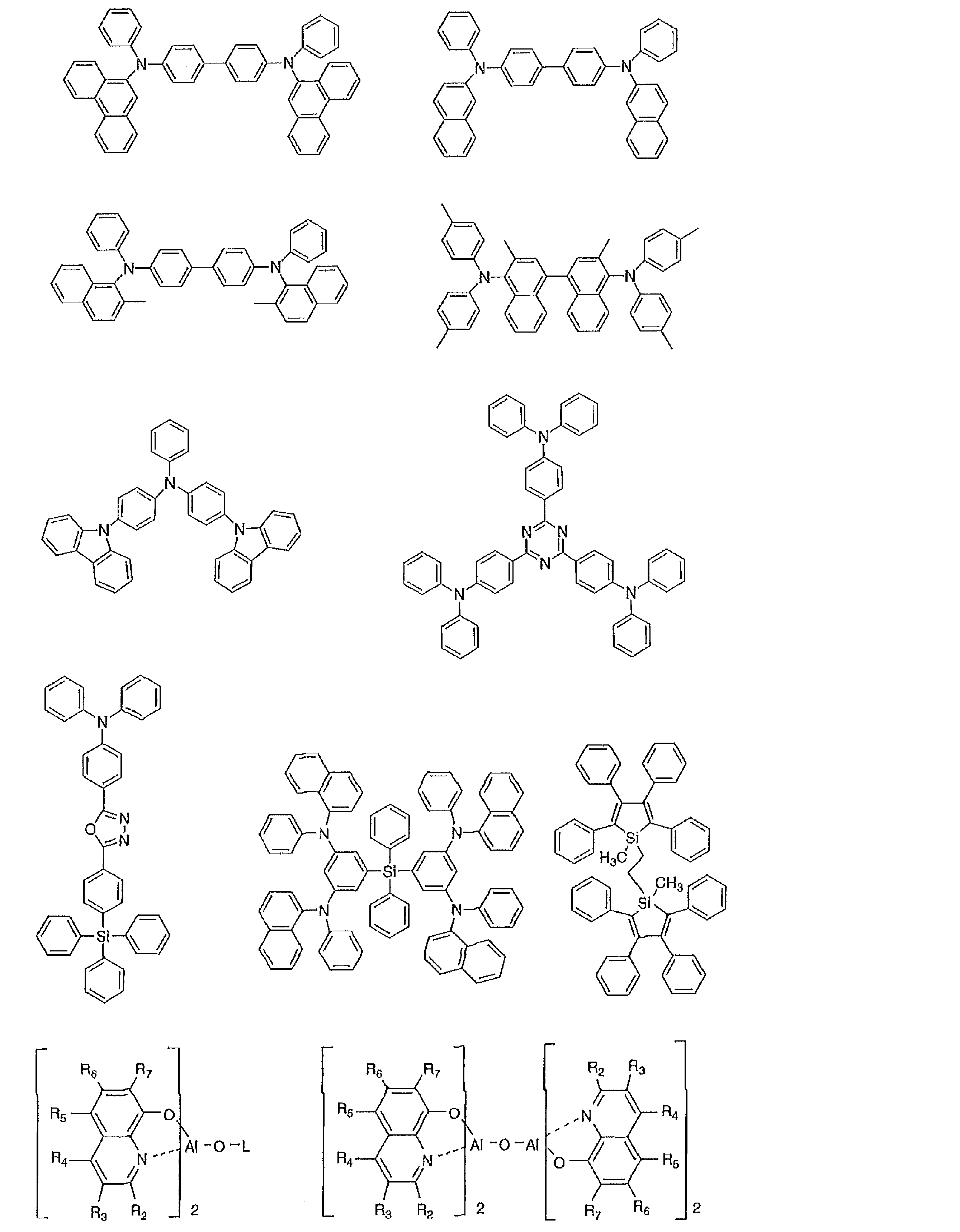
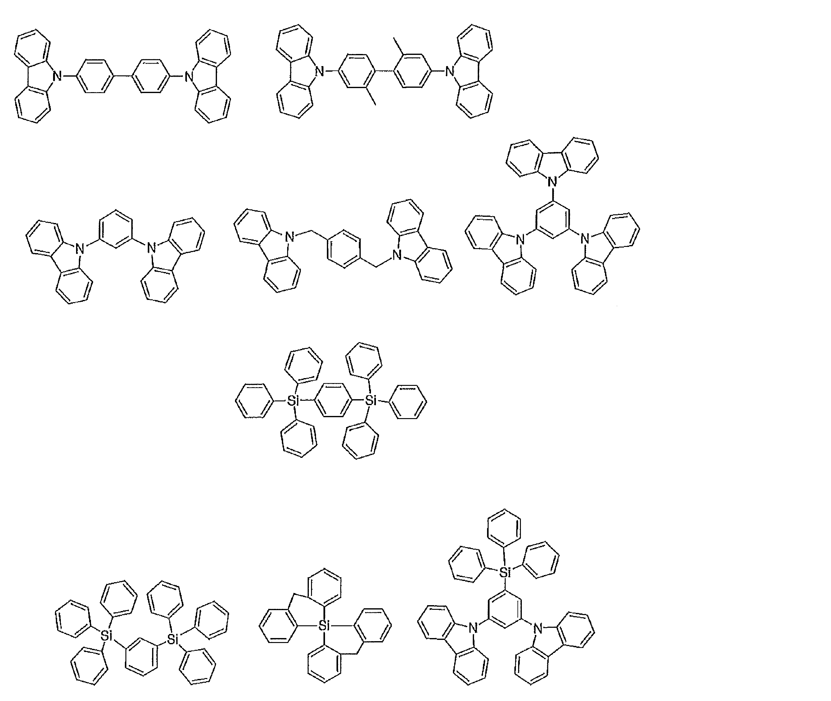
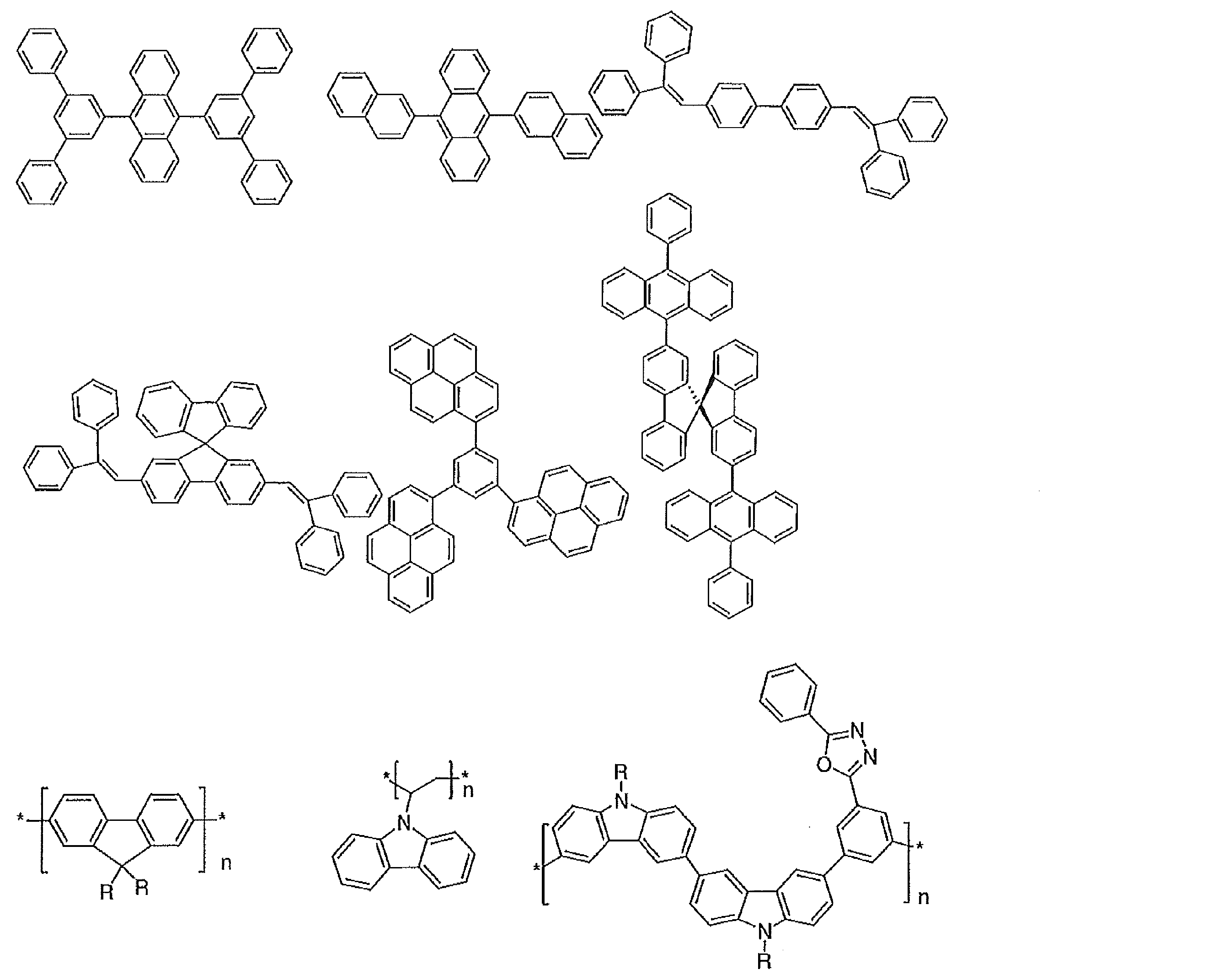
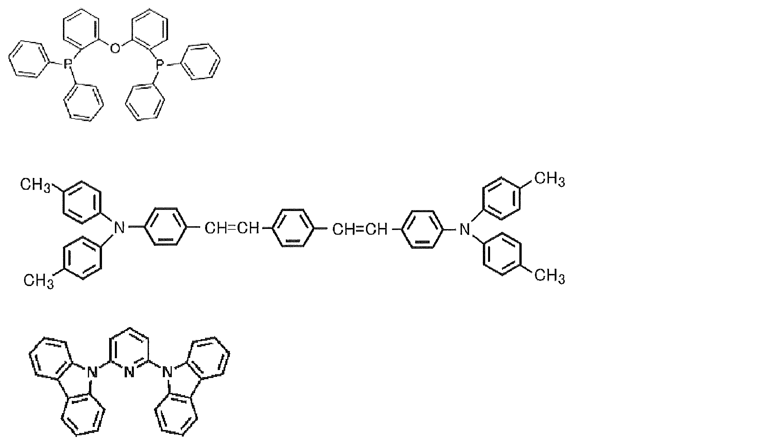
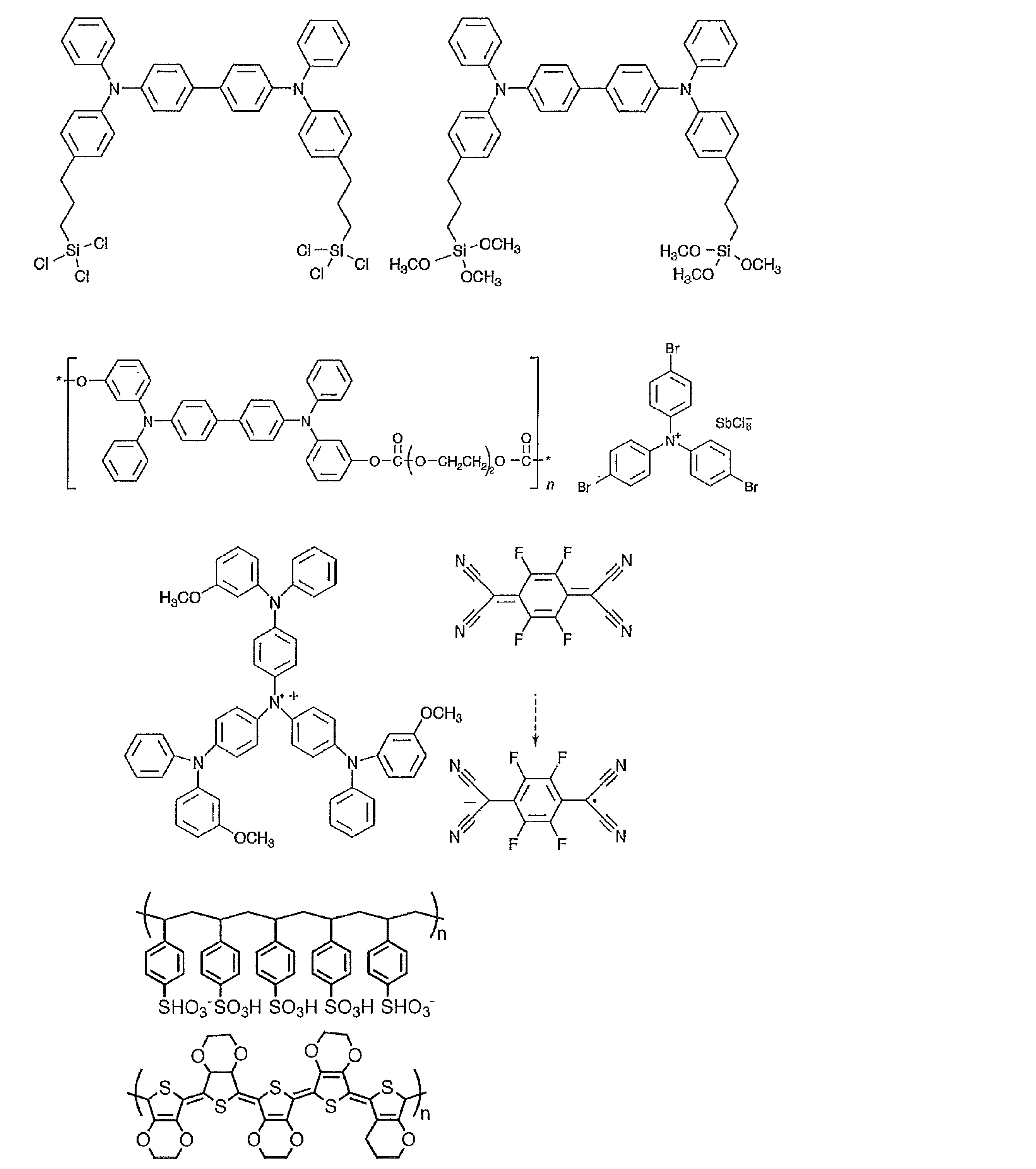

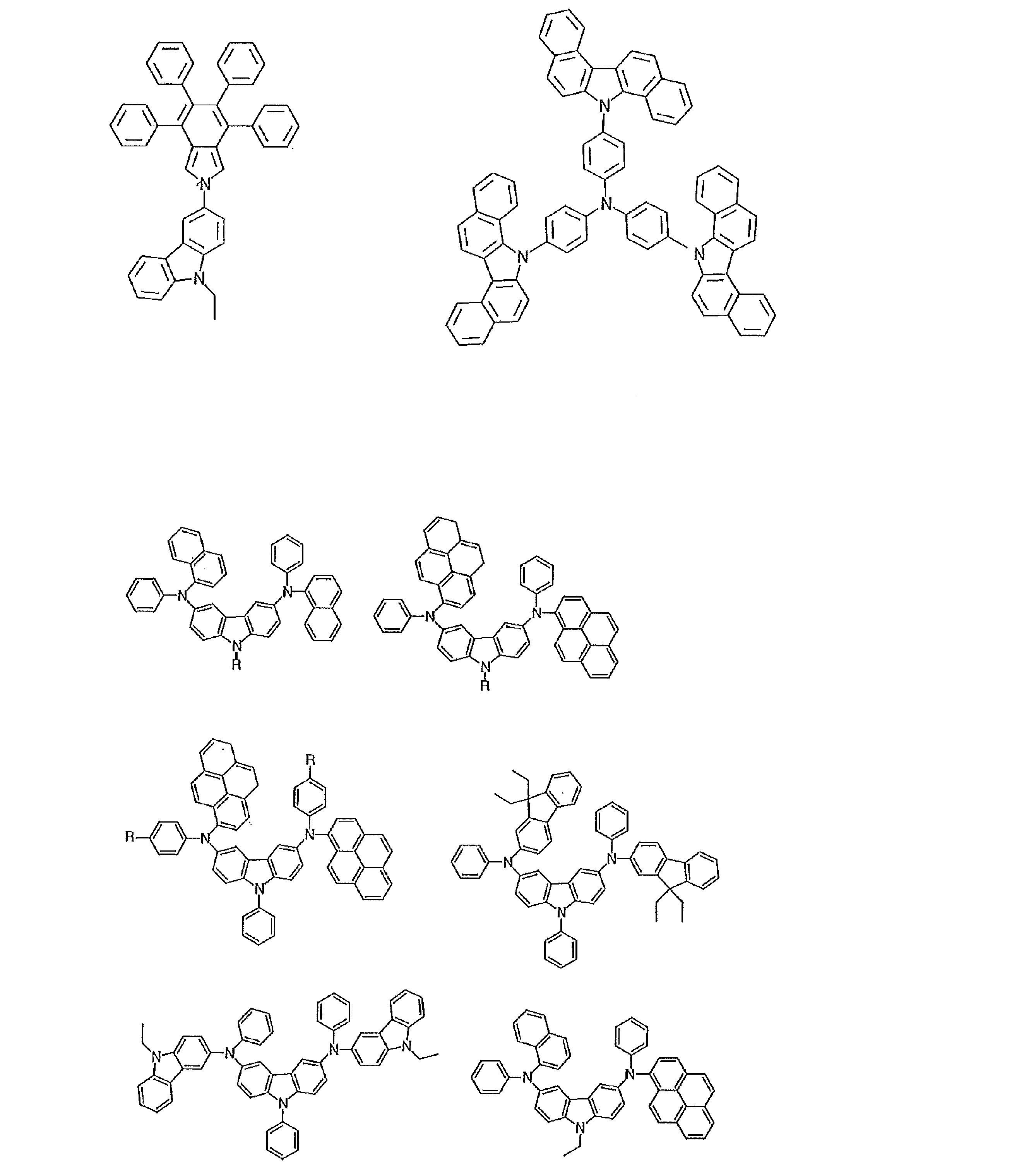

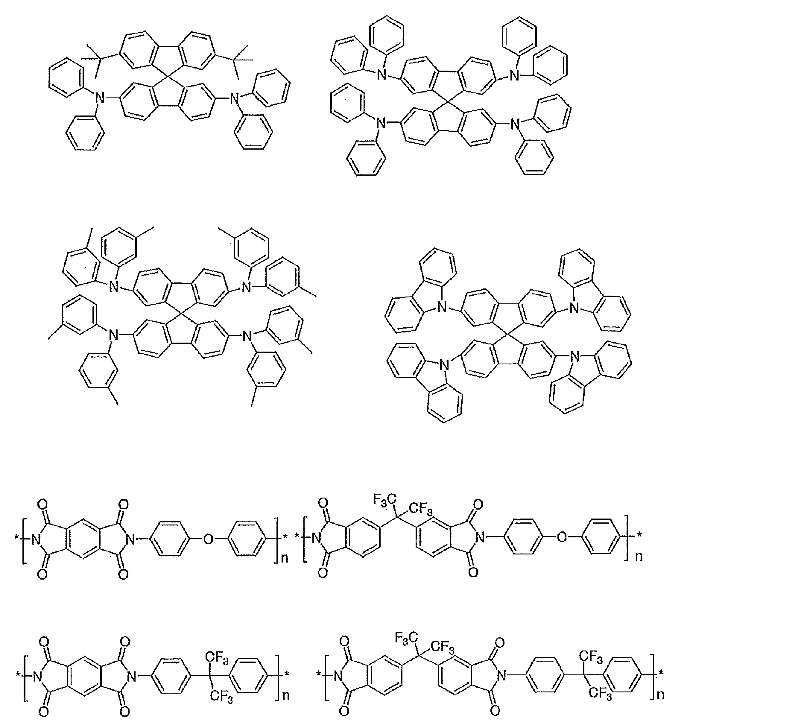
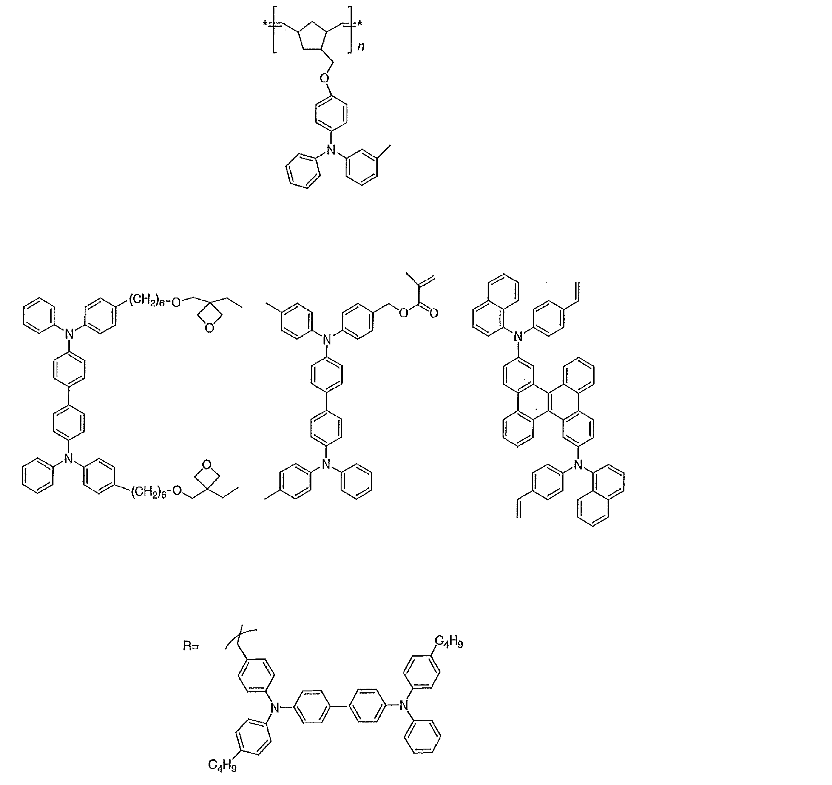


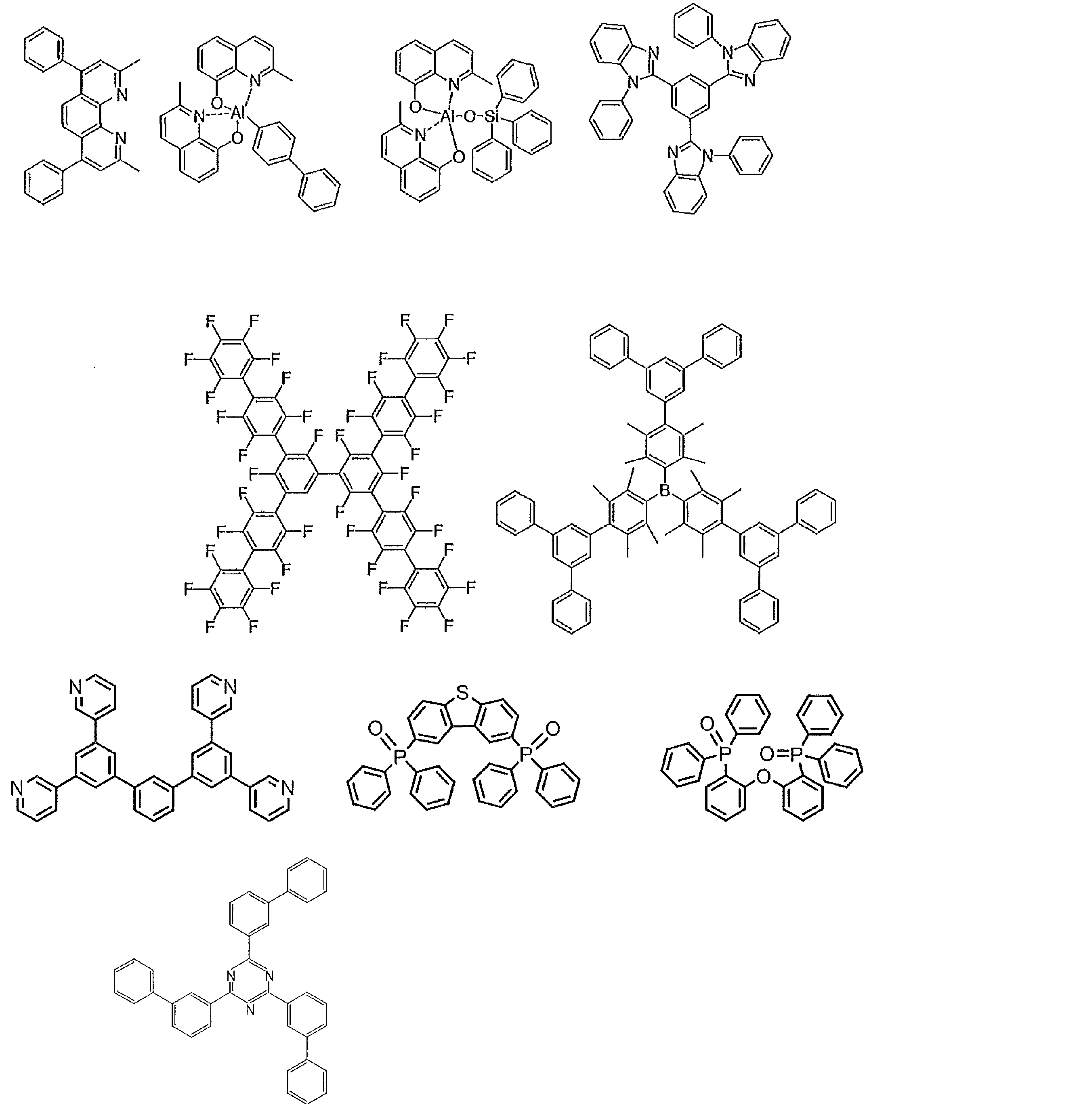
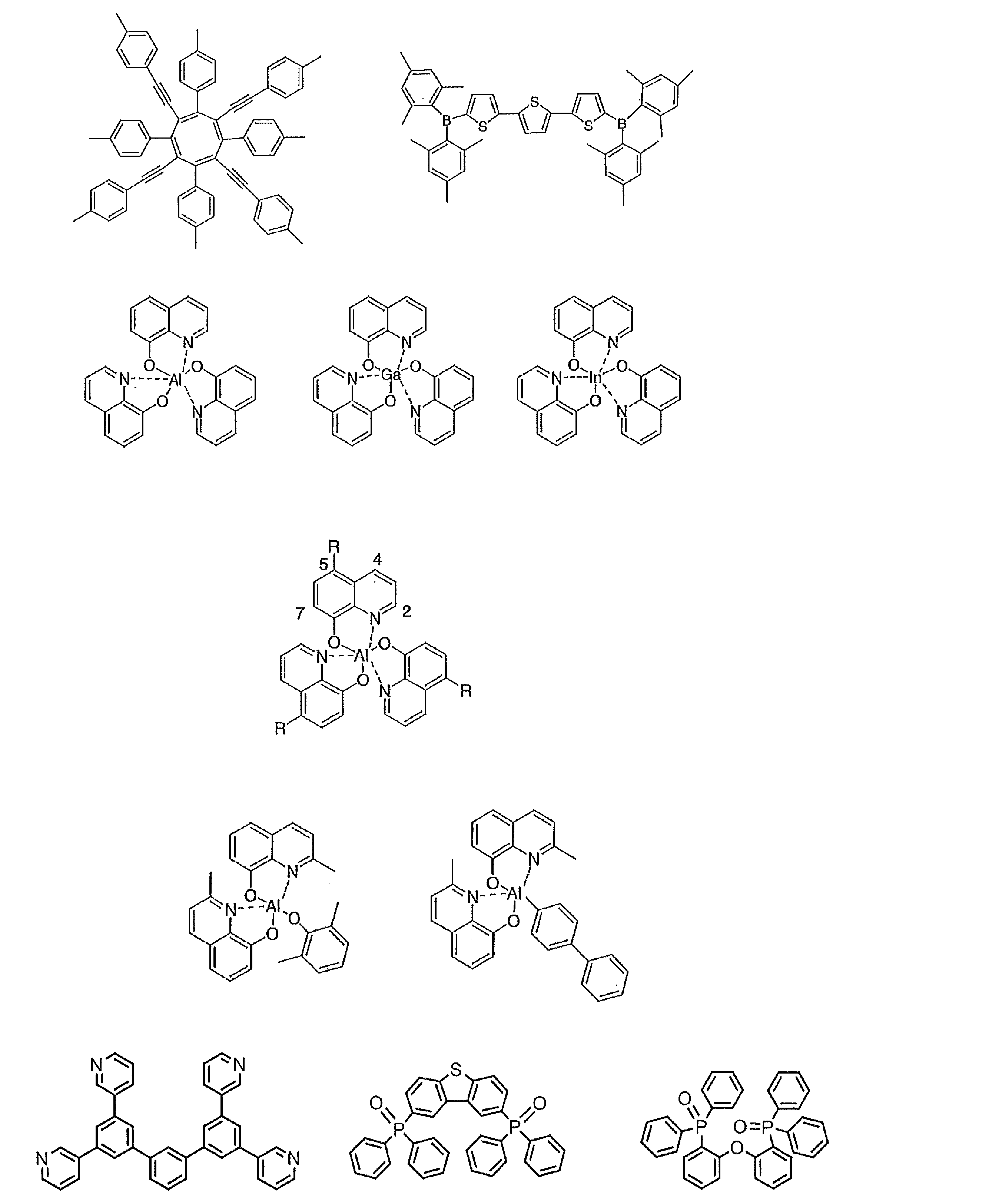
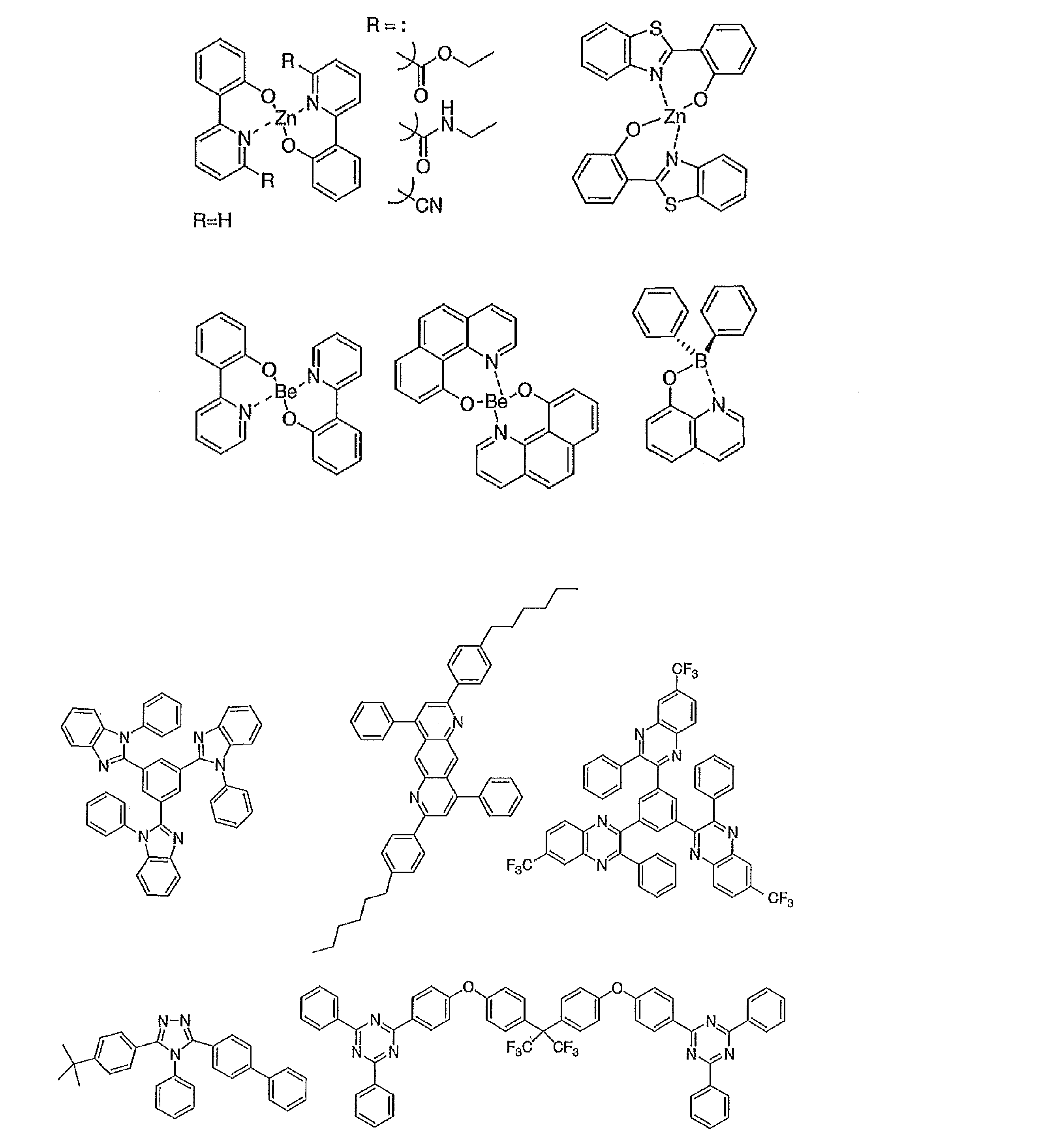
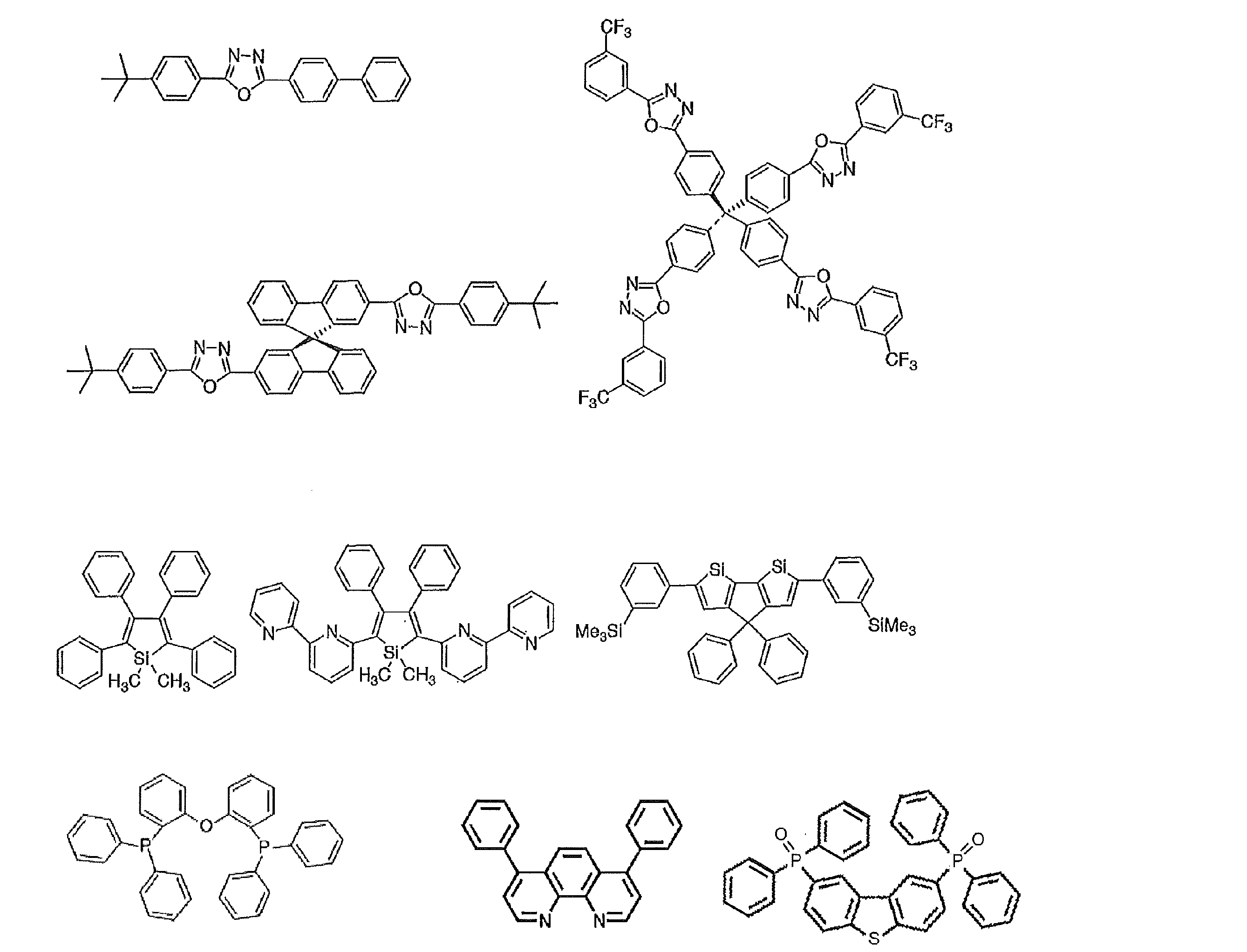


一方、りん光については、本発明の化合物のような通常の有機化合物では、励起三重項エネルギーは不安定で熱等に変換され、寿命が短く直ちに失活するため、室温では殆ど観測できない。通常の有機化合物の励起三重項エネルギーを測定するためには、極低温の条件での発光を観測することにより測定可能である。
化合物1、mCP、および非特許文献1に具体的な構造が記載されている3つのシクロトリホスファゼン化合物(後掲の化合物CP1、CP2、CP3)の各々について、徐々に温度を上昇させて5重量%の重量減少が認められる温度を確認することにより分解温度を測定した。その結果、化合物1の分解温度は474℃で極めて高かったのに対して、mCPは55℃であった。また、非特許文献1のシクロトリホスファゼン化合物の分解温度は280~330℃であることが報告されている。以上より、本発明の化合物1の熱安定性が極めて高いことが確認された。
化合物1の塩化メチレン溶液(濃度10-4mol/L)を77°Kに冷却してPLスペクトルを測定した。PLスペクトルの最も短波側のピーク値のエネルギーを算出し、それを化合物のT1レベル(最低励起三重項エネルギー準位)とした。化合物1のT1レベルは3.00eVであった(HOMO:6.48eV、LUMO:2.52eV)。一方、Appl. Phys. Lett., 2003, 82, 2422にてmCPのT1レベルは2.9eVであることが報告されている(HOMO:5.9eV、LUMO:2.4eV)。
(実施例1)
シリコン基板上に真空蒸着法にて、真空度5.0×10⁻⁴Paの条件にて化合物1と2CzCNとを異なる蒸着源から蒸着し、2CzCNの濃度が3.0重量%である薄膜を0.3nm/秒にて100nmの厚さで形成して有機フォトルミネッセンス素子とした。作製した有機フォトルミネッセンス素子について、紫外励起光による発光スペクトルを測定した結果を図2に示す。フォトルミネッセンス量子効率は大気下で66.0%、窒素雰囲気下で84.8%であった。
(実施例2)
膜厚100nmのインジウム・スズ酸化物(ITO)からなる陽極が形成されたガラス基板上に、各薄膜を真空蒸着法にて、真空度5.0×10⁻⁴Paで積層した。まず、ITO上にα-NPDを35nmの厚さに形成し、その上にmCPを10nmの厚さに形成した。次に、化合物1と2CzCNを異なる蒸着源から共蒸着し、20nmの厚さの層を形成して発光層とした。この時、2CzCNの濃度は3.0重量%とした。次に、PPTを40nmの厚さに形成し、さらにLiFを0.8nm真空蒸着し、次いでアルミニウム(Al)を80nmの厚さに蒸着することにより陰極を形成し、有機エレクトロルミネッセンス素子とした。
作製した有機エレクトロルミネッセンス素子の発光スペクトルを図3に示し、電流密度-電圧-輝度特性を図4に示し、電流密度-外部量子効率特性を図5に示す。最大輝度は18805cd/m2、外部量子効率は14.9%で極めて高かった。仮に発光量子効率が100%の蛍光材料を用いてバランスの取れた理想的な有機エレクトロルミネッセンス素子を試作したとすると、光取り出し効率が20~30%であれば、蛍光発光の外部量子効率は5~7.5%となる。この値が一般に、蛍光材料を用いた有機エレクトロルミネッセンス素子の外部量子効率の理論限界値とされている。化合物1を用いた本発明の有機エレクトロルミネッセンス素子は、理論限界値を超える高い外部量子効率を実現している点で極めて優れている。
化合物1のかわりにmCPを用いて実施例2と同様の方法により有機エレクトロルミネッセンス素子を作製し、同様に特性を評価した。発光スペクトルを図3に示し、電流密度-電圧-輝度特性を図4に示し、電流密度-外部量子効率特性を図5に示す。最大輝度は16524cd/m2、外部量子効率は11.8%であった。
mCPよりも化合物1を用いた方が優れた有機エレクトロルミネッセンス素子を提供できることが確認された。
化合物1のかわりにtBuCzPOを用いて実施例2と同様の方法により有機エレクトロルミネッセンス素子を作製し、同様に特性を評価した。電流密度-電圧-輝度特性を図6に示し、電流密度-外部量子効率特性を図7に示す。最大輝度は6436cd/m2、外部量子効率は12.8%であった。
tBuCzPOよりも化合物1を用いた方が優れた有機エレクトロルミネッセンス素子を提供できることが確認された。
膜厚100nmのインジウム・スズ酸化物(ITO)からなる陽極が形成されたガラス基板上に、各薄膜を真空蒸着法にて、真空度5.0×10⁻⁴Paで積層した。まず、ITO上にα-NPDを35nmの厚さに形成し、その上にmCPを10nmの厚さに形成した。次に、化合物1と4CzIPNを異なる蒸着源から共蒸着し、20nmの厚さの層を形成して発光層とした。この時、4CzIPNの濃度は3.0重量%とした。次に、PPTを40nmの厚さに形成し、さらにLiFを0.8nm真空蒸着し、次いでアルミニウム(Al)を80nmの厚さに蒸着することにより陰極を形成し、有機エレクトロルミネッセンス素子とした。
作製した有機エレクトロルミネッセンス素子の発光スペクトルを図8に示し、電流密度-電圧-輝度特性を図9に示し、電流密度-外部量子効率特性を図10に示す。最大輝度は54141cd/m2、外部量子効率は17.8%で極めて高かった。
化合物1のかわりにmCPを用いて実施例3と同様の方法により有機エレクトロルミネッセンス素子を作製し、同様に特性を評価した。発光スペクトルを図8に示し、電流密度-電圧-輝度特性を図9に示し、電流密度-外部量子効率特性を図10に示す。最大輝度は49176cd/m2、外部量子効率は17.7%であった。
mCPよりも化合物1を用いた方が優れた有機エレクトロルミネッセンス素子を提供できることが確認された。
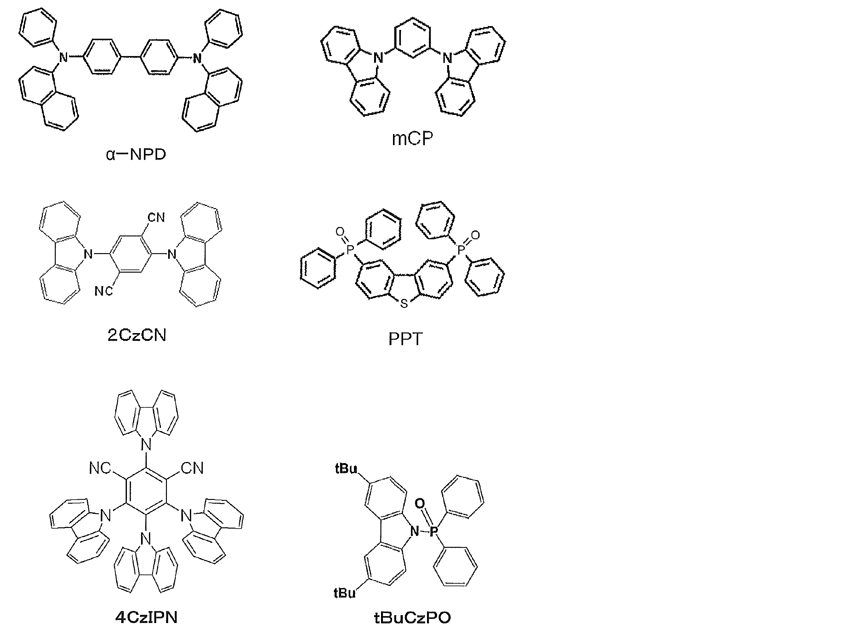
2 陽極
3 正孔注入層
4 正孔輸送層
5 発光層
6 電子輸送層
7 陰極
Claims (15)
- 下記一般式(1)で表される化合物からなる電荷輸送材料。
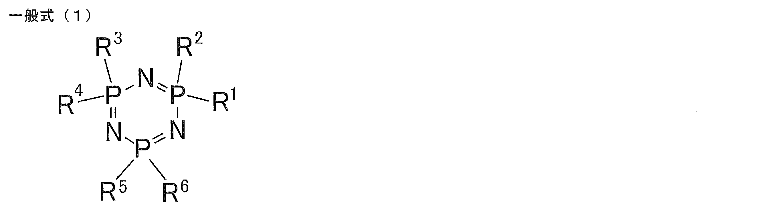

- 一般式(1)のR1~R6がすべて同一であることを特徴とする請求項1に記載の電荷輸送材料。
- 一般式(1)のR1~R6が下記一般式(3)~(7)のいずれかで表される基であることを特徴とする請求項1または2に記載の電荷輸送材料。

- 一般式(1)のR1~R6が前記一般式(3)で表される基であることを特徴とする請求項3に記載の電荷輸送材料。
- 一般式(1)のR1~R6が下記一般式(8)で表される基であることを特徴とする請求項3または4に記載の電荷輸送材料。

- 下記の構造を有する化合物からなることを特徴とする請求項5に記載の電荷輸送材料。

- 請求項1~6のいずれか1項に記載の電荷輸送材料からなることを特徴とするホスト材料。
- 青色発光材料用であることを特徴とする請求項7に記載のホスト材料。
- 請求項7に記載のホスト材料と発光材料を含むことを特徴とする薄膜。
- 前記発光材料が青色発光材料であることを特徴とする請求項9に記載の薄膜。
- 請求項1~6のいずれか1項に記載の電荷輸送材料を用いたことを特徴とする有機発光素子。
- 前記電荷輸送材料をホスト材料として発光層に用いたことを特徴とする請求項11に記載の有機発光素子。
- リン光を放射することを特徴とする請求項11または12に記載の有機発光素子。
- 遅延蛍光を放射することを特徴とする請求項11または12に記載の有機発光素子。
- 有機エレクトロルミネッセンス素子であることを特徴とする請求項11~14のいずれか1項に記載の有機発光素子。
Priority Applications (3)
| Application Number | Priority Date | Filing Date | Title |
|---|---|---|---|
| JP2015504322A JP6305391B2 (ja) | 2013-03-05 | 2014-03-04 | 電荷輸送材料、ホスト材料、薄膜および有機発光素子 |
| CN201480010314.8A CN105027314B (zh) | 2013-03-05 | 2014-03-04 | 电荷传输材料、主体材料、薄膜及有机发光元件 |
| US14/772,802 US9634262B2 (en) | 2013-03-05 | 2014-03-04 | Charge transport material, host material, thin film and organic light emitting element |
Applications Claiming Priority (2)
| Application Number | Priority Date | Filing Date | Title |
|---|---|---|---|
| JP2013-043533 | 2013-03-05 | ||
| JP2013043533 | 2013-03-05 |
Publications (1)
| Publication Number | Publication Date |
|---|---|
| WO2014136758A1 true WO2014136758A1 (ja) | 2014-09-12 |
Family
ID=51491274
Family Applications (1)
| Application Number | Title | Priority Date | Filing Date |
|---|---|---|---|
| PCT/JP2014/055427 WO2014136758A1 (ja) | 2013-03-05 | 2014-03-04 | 電荷輸送材料、ホスト材料、薄膜および有機発光素子 |
Country Status (5)
| Country | Link |
|---|---|
| US (1) | US9634262B2 (ja) |
| JP (1) | JP6305391B2 (ja) |
| CN (1) | CN105027314B (ja) |
| TW (1) | TW201443072A (ja) |
| WO (1) | WO2014136758A1 (ja) |
Cited By (22)
| Publication number | Priority date | Publication date | Assignee | Title |
|---|---|---|---|---|
| JP2016119355A (ja) * | 2014-12-19 | 2016-06-30 | コニカミノルタ株式会社 | 有機エレクトロルミネッセンス素子 |
| CN107210364A (zh) * | 2015-01-19 | 2017-09-26 | 西门子公司 | 氨基磷腈碱作为有机电子产品中的n型掺杂剂 |
| US20180337347A1 (en) * | 2014-02-28 | 2018-11-22 | Kyulux, Inc. | Light-emitting material, organic light-emitting device, and compound |
| WO2020076796A1 (en) | 2018-10-09 | 2020-04-16 | Kyulux, Inc. | Novel composition of matter for use in organic light-emitting diodes |
| JP2020514401A (ja) * | 2016-12-26 | 2020-05-21 | 青島科技大学 | オリゴホスファゼン化合物及びその調製方法と用途 |
| WO2021157642A1 (ja) | 2020-02-04 | 2021-08-12 | 株式会社Kyulux | ホスト材料、組成物および有機発光素子 |
| US11101440B2 (en) | 2015-07-01 | 2021-08-24 | Kyushu University, National University Corporation | Organic electroluminescent device |
| WO2021235549A1 (ja) | 2020-05-22 | 2021-11-25 | 株式会社Kyulux | 化合物、発光材料および発光素子 |
| WO2022025248A1 (ja) | 2020-07-31 | 2022-02-03 | 株式会社Kyulux | 化合物、発光材料および発光素子 |
| US11335872B2 (en) | 2016-09-06 | 2022-05-17 | Kyulux, Inc. | Organic light-emitting device |
| WO2022168956A1 (ja) | 2021-02-04 | 2022-08-11 | 株式会社Kyulux | 化合物、発光材料および有機発光素子 |
| US11476435B2 (en) | 2017-08-24 | 2022-10-18 | Kyushu University, National University Corporation | Film and organic light-emitting device containing perovskite-type compound and organic light-emitting material |
| US11482679B2 (en) | 2017-05-23 | 2022-10-25 | Kyushu University, National University Corporation | Compound, light-emitting lifetime lengthening agent, use of n-type compound, film and light-emitting device |
| WO2022244503A1 (ja) | 2021-05-20 | 2022-11-24 | 株式会社Kyulux | 有機発光素子 |
| WO2022270602A1 (ja) | 2021-06-23 | 2022-12-29 | 株式会社Kyulux | 有機発光素子および膜 |
| WO2022270354A1 (ja) | 2021-06-23 | 2022-12-29 | 株式会社Kyulux | 化合物、発光材料および有機発光素子 |
| WO2023282224A1 (ja) | 2021-07-06 | 2023-01-12 | 株式会社Kyulux | 有機発光素子およびその設計方法 |
| WO2023053835A1 (ja) | 2021-09-28 | 2023-04-06 | 株式会社Kyulux | 化合物、組成物、ホスト材料、電子障壁材料および有機発光素子 |
| WO2023090288A1 (ja) | 2021-11-19 | 2023-05-25 | 株式会社Kyulux | 化合物、発光材料および発光素子 |
| WO2023140130A1 (ja) | 2022-01-19 | 2023-07-27 | 株式会社Kyulux | 化合物、発光材料および有機発光素子 |
| US11930654B2 (en) | 2017-07-06 | 2024-03-12 | Kyulux, Inc. | Organic light-emitting element |
| US12048175B2 (en) | 2015-12-28 | 2024-07-23 | Kyushu University, National University Corporation | Organic electroluminescent device |
Families Citing this family (7)
| Publication number | Priority date | Publication date | Assignee | Title |
|---|---|---|---|---|
| KR101519317B1 (ko) * | 2015-03-27 | 2015-05-18 | 한양대학교 산학협력단 | 온도센서 및 그 제조방법 |
| CN106398682A (zh) * | 2016-03-21 | 2017-02-15 | 北京理工大学 | 一种以三聚磷腈为核的星形有机蓝光材料及其制备方法 |
| CN108239117B (zh) * | 2016-12-26 | 2020-08-14 | 青岛博远高分子材料研究院有限公司 | 环状寡聚磷腈化合物及其制备方法和用途 |
| JP7165431B2 (ja) | 2018-04-11 | 2022-11-04 | 株式会社Kyulux | 量子ドット及び熱活性化遅延蛍光分子を有するトップエミッション型印刷ディスプレイ |
| CN112236498A (zh) | 2018-04-11 | 2021-01-15 | 纳米技术有限公司 | 用于荧光供体辅助oled装置的量子点构造 |
| CN113227316A (zh) | 2018-11-16 | 2021-08-06 | 九州有机光材股份有限公司 | 电致发光显示器件及其制造方法 |
| KR20210136224A (ko) | 2020-05-06 | 2021-11-17 | 삼성디스플레이 주식회사 | 발광 소자 및 이를 포함하는 전자 장치 |
Citations (4)
| Publication number | Priority date | Publication date | Assignee | Title |
|---|---|---|---|---|
| JPH05310949A (ja) * | 1992-05-08 | 1993-11-22 | Toppan Printing Co Ltd | ポリフォスファゼン化合物 |
| JPH06200244A (ja) * | 1992-11-11 | 1994-07-19 | Toppan Printing Co Ltd | 有機薄膜el素子 |
| JPH08283416A (ja) * | 1995-04-14 | 1996-10-29 | Junko Shigehara | 環状ホスファゼン化合物および有機薄膜el素子 |
| JP2006278549A (ja) * | 2005-03-28 | 2006-10-12 | Fuji Photo Film Co Ltd | 有機el素子及び有機elディスプレイ |
Family Cites Families (2)
| Publication number | Priority date | Publication date | Assignee | Title |
|---|---|---|---|---|
| JP2002265614A (ja) | 2001-03-09 | 2002-09-18 | Sumitomo Bakelite Co Ltd | アニオン潜伏性触媒、およびそれを用いた熱硬化性樹脂組成物 |
| KR20110043581A (ko) | 2008-06-20 | 2011-04-27 | 바스프 에스이 | 환형 포스파젠 화합물 및 유기 발광 다이오드에서 이의 용도 |
-
2014
- 2014-03-04 JP JP2015504322A patent/JP6305391B2/ja active Active
- 2014-03-04 US US14/772,802 patent/US9634262B2/en active Active
- 2014-03-04 CN CN201480010314.8A patent/CN105027314B/zh active Active
- 2014-03-04 WO PCT/JP2014/055427 patent/WO2014136758A1/ja active Application Filing
- 2014-03-05 TW TW103107523A patent/TW201443072A/zh unknown
Patent Citations (4)
| Publication number | Priority date | Publication date | Assignee | Title |
|---|---|---|---|---|
| JPH05310949A (ja) * | 1992-05-08 | 1993-11-22 | Toppan Printing Co Ltd | ポリフォスファゼン化合物 |
| JPH06200244A (ja) * | 1992-11-11 | 1994-07-19 | Toppan Printing Co Ltd | 有機薄膜el素子 |
| JPH08283416A (ja) * | 1995-04-14 | 1996-10-29 | Junko Shigehara | 環状ホスファゼン化合物および有機薄膜el素子 |
| JP2006278549A (ja) * | 2005-03-28 | 2006-10-12 | Fuji Photo Film Co Ltd | 有機el素子及び有機elディスプレイ |
Non-Patent Citations (2)
| Title |
|---|
| H. J. BOLINK ET AL.: "EFFICIENT BLUE EMITTING ORGANIC LIGHT EMITTING DIODES BASED ON FLUORESCENT SOLUTION PROCESSABLE CYCLIC PHOSPHAZENES", ORGANIC ELECTRONICS, vol. 9, no. 2, 25 October 2007 (2007-10-25), pages 155 - 163, XP022489968, DOI: doi:10.1016/j.orgel.2007.10.005 * |
| H. J. BOLINK ET AL.: "SOLUTION PROCESSABLE PHOSPHORESCENT DENDRIMERS BASED ON CYCLIC PHOSPHAZENES FOR USE IN ORGANIC LIGHT EMITTING DIODES (OLEDS", CHEMICAL COMMUNICATIONS, 4 December 2007 (2007-12-04), pages 618 - 620 * |
Cited By (28)
| Publication number | Priority date | Publication date | Assignee | Title |
|---|---|---|---|---|
| US20180337347A1 (en) * | 2014-02-28 | 2018-11-22 | Kyulux, Inc. | Light-emitting material, organic light-emitting device, and compound |
| JP2016119355A (ja) * | 2014-12-19 | 2016-06-30 | コニカミノルタ株式会社 | 有機エレクトロルミネッセンス素子 |
| CN107210364A (zh) * | 2015-01-19 | 2017-09-26 | 西门子公司 | 氨基磷腈碱作为有机电子产品中的n型掺杂剂 |
| JP2018505162A (ja) * | 2015-01-19 | 2018-02-22 | シーメンス アクチエンゲゼルシヤフトSiemens Aktiengesellschaft | 有機エレクトロニクスにおけるn−ドーパントとしてのアミノフォスファゼン塩基 |
| US10230050B2 (en) | 2015-01-19 | 2019-03-12 | Siemens Aktiengesellschaft | Amino phosphazene bases as n-dopants in organic electronics |
| CN107210364B (zh) * | 2015-01-19 | 2021-05-04 | 西门子公司 | 氨基磷腈碱作为有机电子产品中的n型掺杂剂 |
| US11101440B2 (en) | 2015-07-01 | 2021-08-24 | Kyushu University, National University Corporation | Organic electroluminescent device |
| US12048175B2 (en) | 2015-12-28 | 2024-07-23 | Kyushu University, National University Corporation | Organic electroluminescent device |
| US11335872B2 (en) | 2016-09-06 | 2022-05-17 | Kyulux, Inc. | Organic light-emitting device |
| JP2020514401A (ja) * | 2016-12-26 | 2020-05-21 | 青島科技大学 | オリゴホスファゼン化合物及びその調製方法と用途 |
| JP7092381B2 (ja) | 2016-12-26 | 2022-06-28 | 青島科技大学 | オリゴホスファゼン化合物及びその調製方法と使用 |
| US11242362B2 (en) | 2016-12-26 | 2022-02-08 | Qingdao University Of Science And Technology | Phosphazene compound, preparation method and use thereof |
| US11482679B2 (en) | 2017-05-23 | 2022-10-25 | Kyushu University, National University Corporation | Compound, light-emitting lifetime lengthening agent, use of n-type compound, film and light-emitting device |
| US11930654B2 (en) | 2017-07-06 | 2024-03-12 | Kyulux, Inc. | Organic light-emitting element |
| US11476435B2 (en) | 2017-08-24 | 2022-10-18 | Kyushu University, National University Corporation | Film and organic light-emitting device containing perovskite-type compound and organic light-emitting material |
| WO2020076796A1 (en) | 2018-10-09 | 2020-04-16 | Kyulux, Inc. | Novel composition of matter for use in organic light-emitting diodes |
| WO2021157642A1 (ja) | 2020-02-04 | 2021-08-12 | 株式会社Kyulux | ホスト材料、組成物および有機発光素子 |
| WO2021157593A1 (ja) | 2020-02-04 | 2021-08-12 | 株式会社Kyulux | 組成物、膜、有機発光素子、発光組成物を提供する方法およびプログラム |
| WO2021235549A1 (ja) | 2020-05-22 | 2021-11-25 | 株式会社Kyulux | 化合物、発光材料および発光素子 |
| WO2022025248A1 (ja) | 2020-07-31 | 2022-02-03 | 株式会社Kyulux | 化合物、発光材料および発光素子 |
| WO2022168956A1 (ja) | 2021-02-04 | 2022-08-11 | 株式会社Kyulux | 化合物、発光材料および有機発光素子 |
| WO2022244503A1 (ja) | 2021-05-20 | 2022-11-24 | 株式会社Kyulux | 有機発光素子 |
| WO2022270354A1 (ja) | 2021-06-23 | 2022-12-29 | 株式会社Kyulux | 化合物、発光材料および有機発光素子 |
| WO2022270602A1 (ja) | 2021-06-23 | 2022-12-29 | 株式会社Kyulux | 有機発光素子および膜 |
| WO2023282224A1 (ja) | 2021-07-06 | 2023-01-12 | 株式会社Kyulux | 有機発光素子およびその設計方法 |
| WO2023053835A1 (ja) | 2021-09-28 | 2023-04-06 | 株式会社Kyulux | 化合物、組成物、ホスト材料、電子障壁材料および有機発光素子 |
| WO2023090288A1 (ja) | 2021-11-19 | 2023-05-25 | 株式会社Kyulux | 化合物、発光材料および発光素子 |
| WO2023140130A1 (ja) | 2022-01-19 | 2023-07-27 | 株式会社Kyulux | 化合物、発光材料および有機発光素子 |
Also Published As
| Publication number | Publication date |
|---|---|
| TW201443072A (zh) | 2014-11-16 |
| JPWO2014136758A1 (ja) | 2017-02-09 |
| CN105027314B (zh) | 2017-09-29 |
| US20160020409A1 (en) | 2016-01-21 |
| JP6305391B2 (ja) | 2018-04-04 |
| US9634262B2 (en) | 2017-04-25 |
| CN105027314A (zh) | 2015-11-04 |
Similar Documents
| Publication | Publication Date | Title |
|---|---|---|
| JP6305391B2 (ja) | 電荷輸送材料、ホスト材料、薄膜および有機発光素子 | |
| JP6277182B2 (ja) | 化合物、発光材料および有機発光素子 | |
| JP6293417B2 (ja) | 化合物、発光材料および有機発光素子 | |
| JP6469076B2 (ja) | 発光材料、有機発光素子および化合物 | |
| JP6262711B2 (ja) | 化合物、発光材料および有機発光素子 | |
| JP6326050B2 (ja) | 化合物、発光材料および有機発光素子 | |
| JP6383538B2 (ja) | 発光材料、有機発光素子および化合物 | |
| JP6367189B2 (ja) | 発光材料、有機発光素子および化合物 | |
| WO2015133501A1 (ja) | 発光材料、有機発光素子および化合物 | |
| WO2015129715A1 (ja) | 発光材料、有機発光素子および化合物 | |
| WO2015108049A1 (ja) | 発光材料、有機発光素子および化合物 | |
| WO2013154064A1 (ja) | 有機発光素子ならびにそれに用いる発光材料および化合物 | |
| WO2013081088A1 (ja) | 有機発光素子ならびにそれに用いる遅延蛍光材料および化合物 | |
| WO2014133121A1 (ja) | 化合物、発光材料および有機発光素子 | |
| WO2014034535A1 (ja) | 発光材料、化合物、およびそれらを用いた有機発光素子 | |
| JP6647514B2 (ja) | 有機発光素子ならびにそれに用いる発光材料および化合物 | |
| WO2018117179A1 (ja) | 有機発光素子、それに用いられる発光材料および遅延蛍光体 | |
| KR20150009512A (ko) | 화합물, 발광 재료 및 유기 발광 소자 | |
| JP2013116975A (ja) | 遅延蛍光材料、有機発光素子および化合物 | |
| WO2018047948A1 (ja) | 有機発光素子ならびにそれに用いる発光材料および化合物 | |
| WO2016111196A1 (ja) | 化合物、混合物、発光層、有機発光素子およびアシストドーパント | |
| WO2018043241A1 (ja) | 有機発光素子ならびにそれに用いる発光材料および化合物 | |
| WO2016035803A1 (ja) | 遅延蛍光体用ホスト材料、有機発光素子および化合物 | |
| WO2018008673A1 (ja) | 有機エレクトロルミネッセンス材料及びこれを用いた有機エレクトロルミネッセンス素子 | |
| JP7395136B2 (ja) | 組成物および有機発光素子 |
Legal Events
| Date | Code | Title | Description |
|---|---|---|---|
| WWE | Wipo information: entry into national phase |
Ref document number: 201480010314.8 Country of ref document: CN |
|
| 121 | Ep: the epo has been informed by wipo that ep was designated in this application |
Ref document number: 14759492 Country of ref document: EP Kind code of ref document: A1 |
|
| ENP | Entry into the national phase |
Ref document number: 2015504322 Country of ref document: JP Kind code of ref document: A |
|
| WWE | Wipo information: entry into national phase |
Ref document number: 14772802 Country of ref document: US |
|
| NENP | Non-entry into the national phase |
Ref country code: DE |
|
| 122 | Ep: pct application non-entry in european phase |
Ref document number: 14759492 Country of ref document: EP Kind code of ref document: A1 |