WO2013161188A1 - Procédé de fabrication de tranche collée - Google Patents
Procédé de fabrication de tranche collée Download PDFInfo
- Publication number
- WO2013161188A1 WO2013161188A1 PCT/JP2013/002278 JP2013002278W WO2013161188A1 WO 2013161188 A1 WO2013161188 A1 WO 2013161188A1 JP 2013002278 W JP2013002278 W JP 2013002278W WO 2013161188 A1 WO2013161188 A1 WO 2013161188A1
- Authority
- WO
- WIPO (PCT)
- Prior art keywords
- wafer
- plasma activation
- stage
- bonded
- bonding
- Prior art date
Links
Images


Classifications
-
- H—ELECTRICITY
- H01—ELECTRIC ELEMENTS
- H01J—ELECTRIC DISCHARGE TUBES OR DISCHARGE LAMPS
- H01J37/00—Discharge tubes with provision for introducing objects or material to be exposed to the discharge, e.g. for the purpose of examination or processing thereof
- H01J37/32—Gas-filled discharge tubes
- H01J37/32009—Arrangements for generation of plasma specially adapted for examination or treatment of objects, e.g. plasma sources
- H01J37/32412—Plasma immersion ion implantation
-
- H—ELECTRICITY
- H01—ELECTRIC ELEMENTS
- H01L—SEMICONDUCTOR DEVICES NOT COVERED BY CLASS H10
- H01L21/00—Processes or apparatus adapted for the manufacture or treatment of semiconductor or solid state devices or of parts thereof
- H01L21/02—Manufacture or treatment of semiconductor devices or of parts thereof
- H01L21/02041—Cleaning
- H01L21/02043—Cleaning before device manufacture, i.e. Begin-Of-Line process
-
- H—ELECTRICITY
- H01—ELECTRIC ELEMENTS
- H01L—SEMICONDUCTOR DEVICES NOT COVERED BY CLASS H10
- H01L21/00—Processes or apparatus adapted for the manufacture or treatment of semiconductor or solid state devices or of parts thereof
- H01L21/67—Apparatus specially adapted for handling semiconductor or electric solid state devices during manufacture or treatment thereof; Apparatus specially adapted for handling wafers during manufacture or treatment of semiconductor or electric solid state devices or components ; Apparatus not specifically provided for elsewhere
- H01L21/683—Apparatus specially adapted for handling semiconductor or electric solid state devices during manufacture or treatment thereof; Apparatus specially adapted for handling wafers during manufacture or treatment of semiconductor or electric solid state devices or components ; Apparatus not specifically provided for elsewhere for supporting or gripping
- H01L21/687—Apparatus specially adapted for handling semiconductor or electric solid state devices during manufacture or treatment thereof; Apparatus specially adapted for handling wafers during manufacture or treatment of semiconductor or electric solid state devices or components ; Apparatus not specifically provided for elsewhere for supporting or gripping using mechanical means, e.g. chucks, clamps or pinches
- H01L21/68714—Apparatus specially adapted for handling semiconductor or electric solid state devices during manufacture or treatment thereof; Apparatus specially adapted for handling wafers during manufacture or treatment of semiconductor or electric solid state devices or components ; Apparatus not specifically provided for elsewhere for supporting or gripping using mechanical means, e.g. chucks, clamps or pinches the wafers being placed on a susceptor, stage or support
- H01L21/6875—Apparatus specially adapted for handling semiconductor or electric solid state devices during manufacture or treatment thereof; Apparatus specially adapted for handling wafers during manufacture or treatment of semiconductor or electric solid state devices or components ; Apparatus not specifically provided for elsewhere for supporting or gripping using mechanical means, e.g. chucks, clamps or pinches the wafers being placed on a susceptor, stage or support characterised by a plurality of individual support members, e.g. support posts or protrusions
-
- H—ELECTRICITY
- H01—ELECTRIC ELEMENTS
- H01L—SEMICONDUCTOR DEVICES NOT COVERED BY CLASS H10
- H01L21/00—Processes or apparatus adapted for the manufacture or treatment of semiconductor or solid state devices or of parts thereof
- H01L21/70—Manufacture or treatment of devices consisting of a plurality of solid state components formed in or on a common substrate or of parts thereof; Manufacture of integrated circuit devices or of parts thereof
- H01L21/71—Manufacture of specific parts of devices defined in group H01L21/70
- H01L21/76—Making of isolation regions between components
- H01L21/762—Dielectric regions, e.g. EPIC dielectric isolation, LOCOS; Trench refilling techniques, SOI technology, use of channel stoppers
- H01L21/7624—Dielectric regions, e.g. EPIC dielectric isolation, LOCOS; Trench refilling techniques, SOI technology, use of channel stoppers using semiconductor on insulator [SOI] technology
- H01L21/76251—Dielectric regions, e.g. EPIC dielectric isolation, LOCOS; Trench refilling techniques, SOI technology, use of channel stoppers using semiconductor on insulator [SOI] technology using bonding techniques
- H01L21/76254—Dielectric regions, e.g. EPIC dielectric isolation, LOCOS; Trench refilling techniques, SOI technology, use of channel stoppers using semiconductor on insulator [SOI] technology using bonding techniques with separation/delamination along an ion implanted layer, e.g. Smart-cut, Unibond
-
- H—ELECTRICITY
- H01—ELECTRIC ELEMENTS
- H01L—SEMICONDUCTOR DEVICES NOT COVERED BY CLASS H10
- H01L21/00—Processes or apparatus adapted for the manufacture or treatment of semiconductor or solid state devices or of parts thereof
- H01L21/02—Manufacture or treatment of semiconductor devices or of parts thereof
- H01L21/02041—Cleaning
- H01L21/02043—Cleaning before device manufacture, i.e. Begin-Of-Line process
- H01L21/02052—Wet cleaning only
-
- H—ELECTRICITY
- H01—ELECTRIC ELEMENTS
- H01L—SEMICONDUCTOR DEVICES NOT COVERED BY CLASS H10
- H01L21/00—Processes or apparatus adapted for the manufacture or treatment of semiconductor or solid state devices or of parts thereof
- H01L21/02—Manufacture or treatment of semiconductor devices or of parts thereof
- H01L21/04—Manufacture or treatment of semiconductor devices or of parts thereof the devices having at least one potential-jump barrier or surface barrier, e.g. PN junction, depletion layer or carrier concentration layer
- H01L21/18—Manufacture or treatment of semiconductor devices or of parts thereof the devices having at least one potential-jump barrier or surface barrier, e.g. PN junction, depletion layer or carrier concentration layer the devices having semiconductor bodies comprising elements of Group IV of the Periodic System or AIIIBV compounds with or without impurities, e.g. doping materials
- H01L21/30—Treatment of semiconductor bodies using processes or apparatus not provided for in groups H01L21/20 - H01L21/26
- H01L21/302—Treatment of semiconductor bodies using processes or apparatus not provided for in groups H01L21/20 - H01L21/26 to change their surface-physical characteristics or shape, e.g. etching, polishing, cutting
- H01L21/306—Chemical or electrical treatment, e.g. electrolytic etching
Definitions
- the present invention relates to a method for manufacturing a bonded wafer using an ion implantation separation method.
- a method for manufacturing a bonded wafer particularly a method for manufacturing a thin film SOI wafer that enables high performance of advanced integrated circuits
- a method of manufacturing an SOI wafer by peeling an ion-implanted wafer after bonding ion implantation separation method: smart
- a technique called a cutting method is attracting attention.
- an oxide film is formed on at least one of two silicon wafers, and gas ions such as hydrogen ions or rare gas ions are implanted from the upper surface of one silicon wafer (bond wafer), After the microbubble layer (encapsulation layer) is formed inside the wafer, the surface into which the ions are implanted is bonded to the other silicon wafer (base wafer) through an oxide film, and then heat treatment ( It is a technology that peels one wafer (bond wafer) into a thin film with a microbubble layer as a cleaved surface by applying exfoliating heat treatment, and further heat-treating (bonding heat treatment) to firmly bond it to an SOI wafer Reference 1).
- the cleaved surface becomes the surface of the SOI layer, and an SOI wafer having a thin SOI film thickness and high uniformity can be obtained relatively easily.
- the bond wafer and the base wafer can also be bonded directly without using an oxide film.
- bonding heat treatment is generally performed after delamination.
- increasing the bonding force before delamination can have a positive effect on quality while the wafer is in close contact.
- We know this, and some ideas to increase the binding power are also considered.
- there is a method of activating the bonding surface before bonding As a method for performing plasma activation processing, an open atmospheric pressure plasma method in which the plasma generating electrode is scanned in the surface in the atmosphere with the wafer placed on the stage, or the wafer is placed on the stage in the chamber, and the pressure in the chamber is reduced. Then, there is a low-pressure plasma method in which plasma is generated by flat plasma generating electrodes arranged opposite to each other while controlling the pressure of nitrogen or oxygen (see, for example, Patent Documents 2-4).
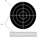
- FIG. 5 shows an outline of a stage of a plasma activation apparatus generally used conventionally.
- the stage 104 has a groove 106 for air venting formed on the surface in contact with the back surface of the wafer, and the area other than the groove 106 is flat. Since this flat portion contacts the wafer, the contact area is large.
- the investigation by the present inventor has revealed that deposits such as particles are increased on the back surface of the wafer after the plasma activation treatment due to contact with the stage.
- the present invention has been made in view of the above-described problems, and suppresses the increase of particles and other deposits on the back surface of the wafer when performing the plasma activation process.
- the wafer after the plasma activation process is prepared.
- An object of the present invention is to provide a method for producing a bonded wafer capable of preventing adhering substances from adhering again to the bonded surface of the wafer when cleaning with a batch type cleaning machine.
- a step of implanting at least one kind of gas ions of hydrogen ions and rare gas ions from the surface of a bond wafer to form an ion implantation layer, and ions of the bond wafer A step of bonding the implanted surface and the surface of the base wafer directly or through an oxide film, and a step of producing a bonded wafer having a thin film on the base wafer by peeling the bond wafer with the ion-implanted layer
- the manufacturing method of a bonded wafer including: a step of performing a plasma activation process on at least one bonded surface of the bond wafer and the base wafer before the bonding step, and the plasma activation In the crystallization process, at least the bond wafer and the base wafer A method for producing a bonded wafer and performing square the plasma activation treatment while placed in a state of being in point contact or line contact with the stage back surface is provided.
- the contact area between the back surface of the wafer and the stage when performing the plasma activation process is reduced, so that an increase in deposits such as particles on the back surface of the wafer can be significantly suppressed. Therefore, even if the wafer after the plasma activation process is cleaned with a batch type cleaning machine, the chance that particles from the back surface reattach to the bonded surface cleaned by plasma activation can be reduced. As a result, it is possible to manufacture a bonded wafer in which the bond strength is increased by plasma activation and surface defects due to deposits sandwiched between the bonded interfaces are suppressed.
- Point contact or line contact can be made by placing at least one of the bond wafer and the base wafer thereon.
- the back surface of the wafer to be processed can be easily placed on the stage with point contact or line contact.
- the bond wafer or the base wafer subjected to the plasma activation treatment is cleaned with a batch type cleaning machine before the bonding step.
- the method for manufacturing a bonded wafer according to the present invention can significantly suppress an increase in deposits on the back surface of the wafer during the plasma activation process. This is extremely effective in avoiding the problem of reattachment of deposits to the bonding surface that may occur during cleaning.
- plasma is placed while placing the back surface of at least one of the bond wafer and the base wafer to be processed in a point contact or line contact state on the stage. Since the activation process is performed, the contact area between the wafer back surface and the stage is reduced, and the increase in deposits such as particles on the back surface side is extremely limited. Thereby, even if the wafer cleaning is performed before the wafer is bonded in the batch type cleaning machine after the plasma activation process, it is possible to reduce the chance that the deposits from the back surface are reattached to the wafer surface cleaned by the plasma activation.
- the bond strength is increased by plasma activation, so that the quality of the bonded wafer can be further improved. Even if the contact between the back surface of the wafer and the stage is a point contact or a line contact, there is no problem in the generation and stability of plasma, and a sufficient plasma irradiation effect can be obtained.
- the present invention is not limited to this.
- the stage used for mounting the wafer is configured to have a large contact area with the back surface of the wafer.
- the inventors' investigation has revealed that this causes an increase in particles adhering to the back surface of the wafer.
- the present inventor has intensively studied to solve this problem.
- the plasma activation processing is performed while the back surface of the plasma activation processing wafer is placed in a point contact or line contact state on the stage of the plasma activation apparatus, thereby placing the processing wafer.
- the present invention has been completed by conceiving that an increase in deposits on the surface side (back surface side) can be suppressed.
- FIG. 1 is a flowchart of an example of a method for producing a bonded wafer according to the present invention.
- a bond wafer 10 and a base wafer 20 serving as a support substrate for example, two silicon single crystal wafers whose both surfaces are mirror-polished are prepared (FIG. 1A).
- the bond wafer 10 and the base wafer 20 are bonded directly or via an oxide film in a later step, but in the case of bonding via an oxide film, at least one of the bond wafer 10 and the base wafer 20 in advance. Then, an oxide film 12 is formed.
- the oxide film 12 can be formed by, for example, thermal oxidation, CVD oxidation, or the like, and becomes, for example, a buried oxide film in a bonded wafer such as an SOI wafer.
- the oxide film 12 is formed only on the bond wafer 10 in FIG. 1, it may be formed only on the base wafer 20 or on both wafers. Further, as shown in FIG. 1, the oxide film 12 may be formed only on the wafer surface side or on the entire surface of the wafer. When the bond wafer 10 and the base wafer 20 are directly bonded together, the oxide film 12 does not need to be formed.
- ion implantation conditions such as implantation energy (ion implantation acceleration voltage), implantation dose, and implantation temperature can be appropriately selected so that a thin film having a predetermined thickness can be obtained.
- FIG. 2 shows an example of a plasma activation apparatus used in the plasma activation process of the bonded wafer manufacturing method of the present invention.
- the plasma activation apparatus 1 includes a parallel plate-shaped upper electrode 3a, a lower electrode 3b and a high-frequency power source 5 for generating plasma, and a stage 4 for mounting a wafer to be processed. These are arranged in the chamber 2.
- a wafer is placed on the lower electrode 3 b, and the lower electrode 3 b plays the role of the stage 4.
- the plasma activation is performed by exposing at least one bonded surface of the wafer to be processed, that is, the bond wafer 10 and the base wafer 20 to the plasma using such a plasma activation apparatus 1.
- the plasma can be, for example, oxygen plasma or nitrogen plasma.
- the wafer to be processed is placed on the stage 4 in a point contact or line contact state, and the plasma activation process is performed in this state.
- the plasma activation process is performed in this state.
- Point contact or line contact is made by placing the wafer. In this way, the contact area between the back surface of the wafer and the stage is reduced, so that it is possible to greatly suppress an increase in deposits such as particles on the back surface side.
- the material of the stage 4 is a metal member (in order to satisfy the requirements of becoming an electrode for generating plasma, preventing metal contamination due to direct contact with the back surface of the wafer, preventing deterioration due to plasma, etc.
- a metal plate) coated with Si can be used.
- the material of the support part and pedestal of the stage 4 described above can be the same as or different from that of the stage 4.
- quartz (SiO 2 ) is preferably used from the viewpoints of preventing metal contamination and preventing deterioration due to plasma. Even when an insulating member such as quartz is used for the support portion and the pedestal of the stage 4, it is preferable that the surface of the metal plate constituting the stage 4 is coated with Si for preventing metal contamination.
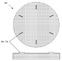
- FIG. 3 shows an example of a stage configured to be in line contact with the wafer back surface.
- the stage 4a in this example six linear protrusions 6a are formed at intervals of 60 degrees on the surface of a metal plate electrode having substantially the same diameter as the wafer to be placed.
- the convex portion 6a is integrally formed with the metal plate electrode, but the columnar or prismatic support portion 7a is manufactured using the same material as the metal plate electrode or an insulating material such as quartz.
- the side surface can be bonded to the surface of the metal plate electrode. Or you may arrange
- the convex portion or the support portion is formed in a columnar shape or a triangular prism shape and the side surface is brought into contact with the wafer back surface, the contact with the wafer back surface becomes a line contact. Further, even in the case of a polygonal column shape of a quadrangular column or more, if the width of the contact portion with the wafer is 3 mm or less, the contact area can be sufficiently reduced, and thus is included in the concept of line contact in the present invention.
- the length of the linear protrusion and the support is longer than these widths, preferably 1/2 or less of the radius of the wafer, and more preferably 1/4 or less of the radius.
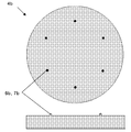
- FIG. 4 shows an example of a stage configured to make point contact with the back surface of the wafer.
- the stage 4b in this example six dot-like convex portions 6b are formed at intervals of 60 degrees on the surface of a metal plate electrode having the same diameter as the wafer to be placed.
- the convex portion 6b is formed integrally with the metal plate electrode.
- a point-like support portion 7b is manufactured using the same material as the metal plate electrode or an insulating material such as quartz, and the surface thereof is formed. It can also be bonded to the surface of the metal plate electrode. Or you may arrange
- the convex portion or the support portion is formed in a spherical shape, a conical shape, or a regular polygonal pyramid shape, and its apex is brought into contact with the wafer back surface, the contact with the wafer back surface becomes a point contact.
- the contact area can be made sufficiently small, so it is included in the concept of point contact in the present invention.
- the support portion is conical, regular polygonal pyramid, cylindrical, or regular polygonal columnar, the bottom surface thereof may be bonded to the surface of the metal plate electrode or fitted into the hole.
- the arrangement of the convex portions or the support portions is 6 at 60 ° intervals, 3 at 120 ° intervals, and 4 at 45 ° intervals at 45 ° intervals. It can also be set at 8 locations and 12 locations at 30 degree intervals.
- the back surface of the wafer is supported by the convex portion or the supporting portion.
- An appropriate space (for example, about 1 mm) is formed between the stage surface and the wafer back surface.
- the wafers that have been plasma-activated in a batch type cleaning machine are cleaned before bonding (FIG. 1 (d)).
- a batch type cleaning machine By using a batch type cleaning machine, a plurality of wafers can be cleaned at a time, so that the process time can be reduced.
- the wafer that has been cleaned by plasma activation in the batch type cleaning which has been a problem in the past, is used. It is possible to avoid the problem that particles from the back surface reattach to the front surface.
- the ion-implanted surface of the bond wafer 10 and the surface of the base wafer 20 are bonded together (FIG. 1 (e)), and the bonded wafer is, for example, 350 ° C. in an inert gas atmosphere.
- a heat treatment including a heat treatment for generating a microbubble layer in the ion implantation layer by holding at a temperature of ⁇ 500 ° C. is performed, the bond wafer 10 is peeled off by the microbubble layer (ion implantation layer), and the thin film 31 is formed on the base wafer 20.
- a bonded wafer 30 having the following is obtained (FIG. 1 (f)).
- the bonded wafer of this invention can suppress that a particle is pinched
- Example 1 As a bond wafer, a silicon single crystal wafer having a diameter of 300 mm, a wafer thickness of 775 ⁇ m, and no COP was prepared. After growing an oxide film of 145 nm, 5 ⁇ 10 H + ions were implanted with an ion implantation machine at an energy of 50 keV. An ion implantation layer was formed by implanting 16 atoms / cm 2 .
- a silicon single crystal wafer similar to the bond wafer but having no oxide film on the surface was prepared, and a plasma activation process using nitrogen plasma was performed.
- a quartz support portion arranged in line contact with the wafer back surface as shown in FIG. 3 was used.
- Si is coated on the surface of a metal lower electrode having the same diameter as that of the base wafer, and cylindrical support portions are formed on the surface at six positions at intervals of 60 degrees as shown in FIG. (2 mm in diameter and 20 mm in length) was placed so that the side surface was in contact with the lower electrode surface.
- a groove (width 2 mm, length 20 mm, depth 1 mm) for fitting the support portion was formed at a position where the columnar support portion on the surface of the lower electrode was arranged.
- the number of particles on the surface of the base wafer was 11 pcs. / Wafer
- the number of particles on the back surface of the base wafer was 800 pcs / wafer.
- the number of particles on the back surface of the base wafer was significantly reduced as compared with 8566 pcs / wafer of a comparative example described later.
- the pre-bonding cleaning was performed using a batch type cleaning machine, with 25 bond wafers as 1 batch and 25 base wafers as 1 batch. After cleaning, when the number of particles on the surface of the base wafer was measured in the same manner as described above, it was reduced to 2 pcs / wafer.
- the surface on the ion implantation side of the bond wafer and the plasma activated surface of the base wafer are adhered and bonded together, and then subjected to heat treatment at a batch temperature of 200 ° C. and a maximum temperature of 500 ° C. in a batch type horizontal heat treatment furnace.
- the bond wafer was peeled off with an ion implantation layer, and an SOI layer was formed on the base wafer to obtain an SOI wafer.
- defect inspection visual void inspection using a void having a diameter of 300 ⁇ m as a limit sample sample
- the manufacturing method of the bonded wafer of the present invention suppresses the increase of the deposits such as particles on the back surface of the wafer when performing the plasma activation process, and batch-process the wafer after the plasma activation process. It was confirmed that it was possible to prevent deposits from reattaching to the bonded surface of the wafer when cleaning with a cleaning machine.
- Example 1 In the plasma activation process, as the stage of the plasma activation device, a stage that is in surface contact with the back surface of the wafer at a portion other than the air vent groove formed on the flat surface as shown in FIG. 5 is used.
- An SOI wafer was manufactured under the same conditions as in Example 1 except that.
- the number of particles of 0.1 ⁇ m or more on the front and back surfaces of the base wafer after the plasma activation treatment was measured, the number of particles on the front surface of the base wafer was 10 pcs / wafer, and the number of particles on the back surface of the base wafer was 8566 pcs / As compared with Example 1, the particle contamination on the back surface was remarkably deteriorated.
- the number of particles on the surface of the base wafer after cleaning in the batch type cleaning machine was measured, it was increased to 25 pcs / wafer.
- the number of particles on the surface of the base wafer after cleaning increased on the contrary.
- a defect inspection of the manufactured SOI wafer was performed, three large voids having a diameter of 300 ⁇ m or more were detected in the SOI wafer. Since a device on the SOI layer cannot be formed at a place where such a void is present, it is often judged as a defective SOI wafer standard.
- Example 2 In the plasma activation process, the same conditions as in Example 1 were used except that a stage having a quartz support portion arranged in point contact with the back surface of the wafer as shown in FIG. 4 was used as the stage of the plasma activation apparatus. An SOI wafer was manufactured. In the stage used, Si was coated on the surface of a metal lower electrode having the same diameter as that of the base wafer, and cylindrical support portions were formed on the surface at six positions at intervals of 60 degrees as shown in FIG. (Diameter 3 mm, height 2 mm) was placed. A hole (diameter 3 mm, depth 1 mm) for fitting the support portion was formed at a position where the columnar support portion on the surface of the lower electrode was arranged.
- Example 1 when the number of particles of 0.1 ⁇ m or more on the front and back surfaces of the base wafer after the plasma activation treatment was measured, the number of particles on the front surface of the base wafer was 10 pcs / wafer, and the number of particles on the back surface of the base wafer was 500 pcs / It was wafer. Further, when the number of particles on the surface of the base wafer after cleaning in the batch type cleaning machine was measured, it was reduced to 3 pcs / wafer. Further, when a defect inspection of the manufactured SOI wafer was performed, no large void having a diameter of 300 ⁇ m or more was detected in the SOI wafer.
- the present invention is not limited to the above embodiment.
- the above-described embodiment is an exemplification, and the present invention has any configuration that has substantially the same configuration as the technical idea described in the claims of the present invention and that exhibits the same effects.
- the point contact or the line contact the case of only the point contact (FIG. 4) and the case of only the line contact (FIG. 3) are shown, but the point contact and the line contact may be mixed. Is possible.
Landscapes
- Engineering & Computer Science (AREA)
- Physics & Mathematics (AREA)
- Microelectronics & Electronic Packaging (AREA)
- General Physics & Mathematics (AREA)
- Manufacturing & Machinery (AREA)
- Computer Hardware Design (AREA)
- Condensed Matter Physics & Semiconductors (AREA)
- Power Engineering (AREA)
- Plasma & Fusion (AREA)
- Chemical & Material Sciences (AREA)
- Analytical Chemistry (AREA)
- Pressure Welding/Diffusion-Bonding (AREA)
- Container, Conveyance, Adherence, Positioning, Of Wafer (AREA)
Abstract
Priority Applications (5)
| Application Number | Priority Date | Filing Date | Title |
|---|---|---|---|
| US14/391,086 US9142449B2 (en) | 2012-04-26 | 2013-04-02 | Method for manufacturing bonded wafer |
| EP13781764.9A EP2843686B1 (fr) | 2012-04-26 | 2013-04-02 | Procédé de fabrication de tranche collée |
| CN201380021381.5A CN104246971B (zh) | 2012-04-26 | 2013-04-02 | 贴合晶片的制造方法 |
| KR1020147029823A KR101855812B1 (ko) | 2012-04-26 | 2013-04-02 | 접합웨이퍼의 제조방법 |
| SG11201406661YA SG11201406661YA (en) | 2012-04-26 | 2013-04-02 | Method for manufacturing bonded wafer |
Applications Claiming Priority (2)
| Application Number | Priority Date | Filing Date | Title |
|---|---|---|---|
| JP2012101768A JP5664592B2 (ja) | 2012-04-26 | 2012-04-26 | 貼り合わせウェーハの製造方法 |
| JP2012-101768 | 2012-04-26 |
Publications (1)
| Publication Number | Publication Date |
|---|---|
| WO2013161188A1 true WO2013161188A1 (fr) | 2013-10-31 |
Family
ID=49482543
Family Applications (1)
| Application Number | Title | Priority Date | Filing Date |
|---|---|---|---|
| PCT/JP2013/002278 WO2013161188A1 (fr) | 2012-04-26 | 2013-04-02 | Procédé de fabrication de tranche collée |
Country Status (7)
| Country | Link |
|---|---|
| US (1) | US9142449B2 (fr) |
| EP (1) | EP2843686B1 (fr) |
| JP (1) | JP5664592B2 (fr) |
| KR (1) | KR101855812B1 (fr) |
| CN (1) | CN104246971B (fr) |
| SG (1) | SG11201406661YA (fr) |
| WO (1) | WO2013161188A1 (fr) |
Cited By (1)
| Publication number | Priority date | Publication date | Assignee | Title |
|---|---|---|---|---|
| CN107633997A (zh) * | 2017-08-10 | 2018-01-26 | 长江存储科技有限责任公司 | 一种晶圆键合方法 |
Families Citing this family (7)
| Publication number | Priority date | Publication date | Assignee | Title |
|---|---|---|---|---|
| JP6213046B2 (ja) * | 2013-08-21 | 2017-10-18 | 信越半導体株式会社 | 貼り合わせウェーハの製造方法 |
| JP6638282B2 (ja) * | 2015-09-25 | 2020-01-29 | 三菱マテリアル株式会社 | 冷却器付き発光モジュールおよび冷却器付き発光モジュールの製造方法 |
| US10269756B2 (en) | 2017-04-21 | 2019-04-23 | Invensas Bonding Technologies, Inc. | Die processing |
| JP6686962B2 (ja) * | 2017-04-25 | 2020-04-22 | 信越半導体株式会社 | 貼り合わせウェーハの製造方法 |
| US10727219B2 (en) | 2018-02-15 | 2020-07-28 | Invensas Bonding Technologies, Inc. | Techniques for processing devices |
| CN109671664A (zh) * | 2018-12-14 | 2019-04-23 | 北京半导体专用设备研究所(中国电子科技集团公司第四十五研究所) | 晶圆载片台 |
| US11742314B2 (en) | 2020-03-31 | 2023-08-29 | Adeia Semiconductor Bonding Technologies Inc. | Reliable hybrid bonded apparatus |
Citations (8)
| Publication number | Priority date | Publication date | Assignee | Title |
|---|---|---|---|---|
| JPS56135934A (en) * | 1980-03-27 | 1981-10-23 | Chiyou Lsi Gijutsu Kenkyu Kumiai | Dry etching device |
| JPH0582404A (ja) | 1991-09-19 | 1993-04-02 | Nippondenso Co Ltd | シリコン基板の接合方法 |
| JP2002313898A (ja) * | 2001-02-08 | 2002-10-25 | Tokyo Electron Ltd | 基板載置台およびその製造方法ならびに処理装置 |
| JP2006339363A (ja) | 2005-06-01 | 2006-12-14 | Bondtech Inc | 表面活性化方法および表面活性化装置 |
| JP2007173354A (ja) * | 2005-12-20 | 2007-07-05 | Shin Etsu Chem Co Ltd | Soi基板およびsoi基板の製造方法 |
| JP2008227207A (ja) * | 2007-03-14 | 2008-09-25 | Sumco Corp | 貼り合わせウェーハの製造方法 |
| JP2009212402A (ja) | 2008-03-06 | 2009-09-17 | Shin Etsu Handotai Co Ltd | 貼り合わせウェーハの製造方法 |
| JP2012038963A (ja) | 2010-08-09 | 2012-02-23 | Sumco Corp | 貼り合わせウェーハの製造方法 |
Family Cites Families (9)
| Publication number | Priority date | Publication date | Assignee | Title |
|---|---|---|---|---|
| US6534380B1 (en) * | 1997-07-18 | 2003-03-18 | Denso Corporation | Semiconductor substrate and method of manufacturing the same |
| DE19929278A1 (de) * | 1998-06-26 | 2000-02-17 | Nissin Electric Co Ltd | Verfahren zum Implantieren negativer Wasserstoffionen und Implantierungseinrichtung |
| KR100730806B1 (ko) * | 1999-10-14 | 2007-06-20 | 신에쯔 한도타이 가부시키가이샤 | Soi웨이퍼의 제조방법 및 soi 웨이퍼 |
| US7176528B2 (en) * | 2003-02-18 | 2007-02-13 | Corning Incorporated | Glass-based SOI structures |
| JP4509488B2 (ja) * | 2003-04-02 | 2010-07-21 | 株式会社Sumco | 貼り合わせ基板の製造方法 |
| US7791708B2 (en) * | 2006-12-27 | 2010-09-07 | Asml Netherlands B.V. | Lithographic apparatus, substrate table, and method for enhancing substrate release properties |
| JP5415676B2 (ja) * | 2007-05-30 | 2014-02-12 | 信越化学工業株式会社 | Soiウェーハの製造方法 |
| EP2200077B1 (fr) * | 2008-12-22 | 2012-12-05 | Soitec | Procédé pour la liaison de deux substrats |
| US8557679B2 (en) * | 2010-06-30 | 2013-10-15 | Corning Incorporated | Oxygen plasma conversion process for preparing a surface for bonding |
-
2012
- 2012-04-26 JP JP2012101768A patent/JP5664592B2/ja active Active
-
2013
- 2013-04-02 KR KR1020147029823A patent/KR101855812B1/ko active IP Right Grant
- 2013-04-02 WO PCT/JP2013/002278 patent/WO2013161188A1/fr active Application Filing
- 2013-04-02 CN CN201380021381.5A patent/CN104246971B/zh active Active
- 2013-04-02 US US14/391,086 patent/US9142449B2/en active Active
- 2013-04-02 SG SG11201406661YA patent/SG11201406661YA/en unknown
- 2013-04-02 EP EP13781764.9A patent/EP2843686B1/fr active Active
Patent Citations (8)
| Publication number | Priority date | Publication date | Assignee | Title |
|---|---|---|---|---|
| JPS56135934A (en) * | 1980-03-27 | 1981-10-23 | Chiyou Lsi Gijutsu Kenkyu Kumiai | Dry etching device |
| JPH0582404A (ja) | 1991-09-19 | 1993-04-02 | Nippondenso Co Ltd | シリコン基板の接合方法 |
| JP2002313898A (ja) * | 2001-02-08 | 2002-10-25 | Tokyo Electron Ltd | 基板載置台およびその製造方法ならびに処理装置 |
| JP2006339363A (ja) | 2005-06-01 | 2006-12-14 | Bondtech Inc | 表面活性化方法および表面活性化装置 |
| JP2007173354A (ja) * | 2005-12-20 | 2007-07-05 | Shin Etsu Chem Co Ltd | Soi基板およびsoi基板の製造方法 |
| JP2008227207A (ja) * | 2007-03-14 | 2008-09-25 | Sumco Corp | 貼り合わせウェーハの製造方法 |
| JP2009212402A (ja) | 2008-03-06 | 2009-09-17 | Shin Etsu Handotai Co Ltd | 貼り合わせウェーハの製造方法 |
| JP2012038963A (ja) | 2010-08-09 | 2012-02-23 | Sumco Corp | 貼り合わせウェーハの製造方法 |
Cited By (6)
| Publication number | Priority date | Publication date | Assignee | Title |
|---|---|---|---|---|
| CN107633997A (zh) * | 2017-08-10 | 2018-01-26 | 长江存储科技有限责任公司 | 一种晶圆键合方法 |
| CN107633997B (zh) * | 2017-08-10 | 2019-01-29 | 长江存储科技有限责任公司 | 一种晶圆键合方法 |
| CN109671614A (zh) * | 2017-08-10 | 2019-04-23 | 长江存储科技有限责任公司 | 一种晶圆键合方法 |
| US10679854B2 (en) | 2017-08-10 | 2020-06-09 | Yangtze Memory Technologies Co., Ltd. | Wafer bonding method and structure thereof |
| CN109671614B (zh) * | 2017-08-10 | 2020-08-21 | 长江存储科技有限责任公司 | 一种晶圆键合方法 |
| US11342185B2 (en) | 2017-08-10 | 2022-05-24 | Yangtze Memory Technologies Co., Ltd. | Wafer bonding method and structure thereof |
Also Published As
| Publication number | Publication date |
|---|---|
| US20150118825A1 (en) | 2015-04-30 |
| EP2843686A1 (fr) | 2015-03-04 |
| KR20150003763A (ko) | 2015-01-09 |
| CN104246971A (zh) | 2014-12-24 |
| KR101855812B1 (ko) | 2018-05-10 |
| CN104246971B (zh) | 2018-06-15 |
| SG11201406661YA (en) | 2014-11-27 |
| EP2843686B1 (fr) | 2019-03-27 |
| JP2013229516A (ja) | 2013-11-07 |
| US9142449B2 (en) | 2015-09-22 |
| EP2843686A4 (fr) | 2016-01-20 |
| JP5664592B2 (ja) | 2015-02-04 |
Similar Documents
| Publication | Publication Date | Title |
|---|---|---|
| JP5664592B2 (ja) | 貼り合わせウェーハの製造方法 | |
| US7674687B2 (en) | Method and structure for fabricating multiple tiled regions onto a plate using a controlled cleaving process | |
| JP5415129B2 (ja) | 貼り合わせ基板の製造方法 | |
| JP2006210898A (ja) | Soiウエーハの製造方法及びsoiウェーハ | |
| US20110132259A1 (en) | Electrostatic chuck and vacuum processing apparatus | |
| KR101541940B1 (ko) | Soi 기판의 제조 방법 | |
| JP2008153411A (ja) | Soi基板の製造方法 | |
| JP2001274368A (ja) | 貼り合わせウエーハの製造方法およびこの方法で製造された貼り合わせウエーハ | |
| JP2010538459A (ja) | 熱処理を用いる剥離プロセスにおける半導体ウエハの再使用 | |
| KR101952982B1 (ko) | 복합 웨이퍼의 제조 방법 | |
| TW201421584A (zh) | 混成基板之製造方法及混成基板 | |
| KR20110052456A (ko) | 웨이퍼 접합 방법 | |
| CN101960558A (zh) | 贴合晶片的制造方法 | |
| JP5667743B2 (ja) | Soi基板の作製方法 | |
| KR20080086899A (ko) | Soi 웨이퍼의 제조 방법 및 soi 웨이퍼 | |
| KR101380514B1 (ko) | 반도체 기판의 제조 방법 | |
| JP2009253184A (ja) | 貼り合わせ基板の製造方法 | |
| EP2030076A2 (fr) | Procédé de formation d'une structure semi-conducteur sur isolant | |
| JP2008263010A (ja) | Soi基板の製造方法 | |
| JP5364345B2 (ja) | Soi基板の作製方法 | |
| TW202343550A (zh) | 將薄層轉移到載體基板之方法 | |
| JP2017212345A (ja) | 半導体製造装置、及び半導体製造方法 | |
| JP2012038963A (ja) | 貼り合わせウェーハの製造方法 | |
| JP2015176899A (ja) | 複合基板の製造方法 |
Legal Events
| Date | Code | Title | Description |
|---|---|---|---|
| 121 | Ep: the epo has been informed by wipo that ep was designated in this application |
Ref document number: 13781764 Country of ref document: EP Kind code of ref document: A1 |
|
| WWE | Wipo information: entry into national phase |
Ref document number: 14391086 Country of ref document: US |
|
| WWE | Wipo information: entry into national phase |
Ref document number: 2013781764 Country of ref document: EP |
|
| ENP | Entry into the national phase |
Ref document number: 20147029823 Country of ref document: KR Kind code of ref document: A |
|
| NENP | Non-entry into the national phase |
Ref country code: DE |