WO2013132889A1 - プラズマcvd法により形成された化学蒸着膜 - Google Patents
プラズマcvd法により形成された化学蒸着膜 Download PDFInfo
- Publication number
- WO2013132889A1 WO2013132889A1 PCT/JP2013/050606 JP2013050606W WO2013132889A1 WO 2013132889 A1 WO2013132889 A1 WO 2013132889A1 JP 2013050606 W JP2013050606 W JP 2013050606W WO 2013132889 A1 WO2013132889 A1 WO 2013132889A1
- Authority
- WO
- WIPO (PCT)
- Prior art keywords
- chemical vapor
- vapor deposition
- film
- deposition film
- layer
- Prior art date
- Legal status (The legal status is an assumption and is not a legal conclusion. Google has not performed a legal analysis and makes no representation as to the accuracy of the status listed.)
- Ceased
Links
Images


Classifications
-
- C—CHEMISTRY; METALLURGY
- C23—COATING METALLIC MATERIAL; COATING MATERIAL WITH METALLIC MATERIAL; CHEMICAL SURFACE TREATMENT; DIFFUSION TREATMENT OF METALLIC MATERIAL; COATING BY VACUUM EVAPORATION, BY SPUTTERING, BY ION IMPLANTATION OR BY CHEMICAL VAPOUR DEPOSITION, IN GENERAL; INHIBITING CORROSION OF METALLIC MATERIAL OR INCRUSTATION IN GENERAL
- C23C—COATING METALLIC MATERIAL; COATING MATERIAL WITH METALLIC MATERIAL; SURFACE TREATMENT OF METALLIC MATERIAL BY DIFFUSION INTO THE SURFACE, BY CHEMICAL CONVERSION OR SUBSTITUTION; COATING BY VACUUM EVAPORATION, BY SPUTTERING, BY ION IMPLANTATION OR BY CHEMICAL VAPOUR DEPOSITION, IN GENERAL
- C23C16/00—Chemical coating by decomposition of gaseous compounds, without leaving reaction products of surface material in the coating, i.e. chemical vapour deposition [CVD] processes
- C23C16/22—Chemical coating by decomposition of gaseous compounds, without leaving reaction products of surface material in the coating, i.e. chemical vapour deposition [CVD] processes characterised by the deposition of inorganic material, other than metallic material
- C23C16/30—Deposition of compounds, mixtures or solid solutions, e.g. borides, carbides, nitrides
- C23C16/40—Oxides
- C23C16/401—Oxides containing silicon
-
- C—CHEMISTRY; METALLURGY
- C23—COATING METALLIC MATERIAL; COATING MATERIAL WITH METALLIC MATERIAL; CHEMICAL SURFACE TREATMENT; DIFFUSION TREATMENT OF METALLIC MATERIAL; COATING BY VACUUM EVAPORATION, BY SPUTTERING, BY ION IMPLANTATION OR BY CHEMICAL VAPOUR DEPOSITION, IN GENERAL; INHIBITING CORROSION OF METALLIC MATERIAL OR INCRUSTATION IN GENERAL
- C23C—COATING METALLIC MATERIAL; COATING MATERIAL WITH METALLIC MATERIAL; SURFACE TREATMENT OF METALLIC MATERIAL BY DIFFUSION INTO THE SURFACE, BY CHEMICAL CONVERSION OR SUBSTITUTION; COATING BY VACUUM EVAPORATION, BY SPUTTERING, BY ION IMPLANTATION OR BY CHEMICAL VAPOUR DEPOSITION, IN GENERAL
- C23C16/00—Chemical coating by decomposition of gaseous compounds, without leaving reaction products of surface material in the coating, i.e. chemical vapour deposition [CVD] processes
- C23C16/44—Chemical coating by decomposition of gaseous compounds, without leaving reaction products of surface material in the coating, i.e. chemical vapour deposition [CVD] processes characterised by the method of coating
- C23C16/50—Chemical coating by decomposition of gaseous compounds, without leaving reaction products of surface material in the coating, i.e. chemical vapour deposition [CVD] processes characterised by the method of coating using electric discharges
- C23C16/505—Chemical coating by decomposition of gaseous compounds, without leaving reaction products of surface material in the coating, i.e. chemical vapour deposition [CVD] processes characterised by the method of coating using electric discharges using radio frequency discharges
-
- H—ELECTRICITY
- H10—SEMICONDUCTOR DEVICES; ELECTRIC SOLID-STATE DEVICES NOT OTHERWISE PROVIDED FOR
- H10F—INORGANIC SEMICONDUCTOR DEVICES SENSITIVE TO INFRARED RADIATION, LIGHT, ELECTROMAGNETIC RADIATION OF SHORTER WAVELENGTH OR CORPUSCULAR RADIATION
- H10F77/00—Constructional details of devices covered by this subclass
- H10F77/50—Encapsulations or containers
-
- H—ELECTRICITY
- H10—SEMICONDUCTOR DEVICES; ELECTRIC SOLID-STATE DEVICES NOT OTHERWISE PROVIDED FOR
- H10K—ORGANIC ELECTRIC SOLID-STATE DEVICES
- H10K59/00—Integrated devices, or assemblies of multiple devices, comprising at least one organic light-emitting element covered by group H10K50/00
- H10K59/80—Constructional details
- H10K59/87—Passivation; Containers; Encapsulations
- H10K59/873—Encapsulations
-
- H—ELECTRICITY
- H10—SEMICONDUCTOR DEVICES; ELECTRIC SOLID-STATE DEVICES NOT OTHERWISE PROVIDED FOR
- H10W—GENERIC PACKAGES, INTERCONNECTIONS, CONNECTORS OR OTHER CONSTRUCTIONAL DETAILS OF DEVICES COVERED BY CLASS H10
- H10W74/00—Encapsulations, e.g. protective coatings
- H10W74/01—Manufacture or treatment
-
- H—ELECTRICITY
- H10—SEMICONDUCTOR DEVICES; ELECTRIC SOLID-STATE DEVICES NOT OTHERWISE PROVIDED FOR
- H10W—GENERIC PACKAGES, INTERCONNECTIONS, CONNECTORS OR OTHER CONSTRUCTIONAL DETAILS OF DEVICES COVERED BY CLASS H10
- H10W74/00—Encapsulations, e.g. protective coatings
- H10W74/40—Encapsulations, e.g. protective coatings characterised by their materials
- H10W74/43—Encapsulations, e.g. protective coatings characterised by their materials comprising oxides, nitrides or carbides, e.g. ceramics or glasses
Definitions
- the present invention relates to a chemical vapor deposition film formed by a plasma CVD method, a laminate including the chemical vapor deposition film, a thin film solar cell, and a method for manufacturing the laminate.
- a gas barrier film exhibiting high barrier properties is generally formed by a plasma CVD method with an organic layer and an inorganic layer, or a laminated structure of inorganic layers.
- Patent Document 2 as a method for forming a barrier film having high adhesion and barrier properties on the surface of a substrate such as a plastic container by plasma CVD, silicon (Si) and carbon (C) are used as the first layer. It has been proposed to form an adhesion enhancing layer made of oxygen (O) and a barrier layer made of silicon oxide as the second layer.
- the plastic film exhibits good adhesion to a single plastic substrate
- the plastic film is formed on the surface on which a barrier film is formed, such as an organic EL element or a solar battery cell that is weak against moisture and oxygen. (Organic material) and metal (inorganic material) mixed, the adhesion to the exposed substrate is insufficient, and the film consisting only of silicon (Si), carbon (C) and oxygen (O),
- a barrier film is easily broken because of its high density and lack of flexibility.
- a first thin film is formed on an electronic device such as a plastic film or an organic EL by a plasma CVD method using a gas containing a hydrogen element and a gas containing a silicon element, and has a barrier function. It is described that a silicon-based thin film having high adhesion and barrier performance can be formed by forming a thin film on the first thin film. Specifically, a film is formed using hexamethyldisilazane (hereinafter sometimes referred to as HMDS), which is an organosilicon compound containing no oxygen atom, and a mixed gas of H 2 and Ar.
- HMDS hexamethyldisilazane
- this film has a problem that the adhesion to the transparent conductive film and the metal film present in the organic EL element, the solar cell and the like is not sufficient, and the barrier film is easily broken.
- the substrate is irradiated with plasma before forming the barrier film to activate the surface.
- the adhesion between the barrier film and the substrate by modifying.
- the base material is significantly deteriorated (oxidation deterioration, etc.) and cannot be used.
- the present invention has been made in view of such problems of the prior art, and has excellent adhesion to not only organic substances but also inorganic substances, and adhesion to both organic and inorganic substances.
- An object of the present invention is to provide a gas barrier film having a high barrier property and a manufacturing method even for a substrate made of an organic material, a substrate made of an inorganic material, and a substrate made of a mixture of an organic material and an inorganic material.
- the present inventors have determined that the first three layers are formed from the substrate side to the first thin film (adhesion layer), the second thin film (flexible layer), and the third thin film (barrier layer).
- the gas barrier film with high adhesion and barrier properties can be formed by using different materials depending on the presence or absence of oxygen atoms in the organosilicon compound molecules when forming the structure and structure and forming each layer.
- organic EL elements and solar cells that are prone to deterioration with respect to moisture and oxygen, especially organic materials (organic power generation layers, light emitting layers, plastic films (PET and PEN), etc.) and inorganic materials (surfaces) It has been found that a barrier film with good adhesion can be formed on a substrate in which a transparent conductive film, a metal electrode, an inorganic power generation layer, etc.) are mixed and exposed without damaging the substrate. It was completed a light.
- the present invention provides a chemical vapor deposition film formed by a plasma CVD method that contains silicon atoms, oxygen atoms, carbon atoms, and hydrogen atoms, and the concentration of the oxygen atoms is 10 to 35 element%.
- the present invention also provides a chemical vapor deposition film as described above; a second chemical vapor deposition film comprising silicon atoms and oxygen atoms of 0 element% or more and less than 10 element% and formed by plasma CVD; silicon atoms and 35 elements And a third chemical vapor deposition film formed by a plasma CVD method, and comprising a second chemical vapor deposition film and a third chemical vapor deposition on one surface of the chemical vapor deposition film.
- the second chemical vapor deposition film preferably contains carbon atoms.
- a substrate containing an inorganic substance is further provided, and the chemical vapor deposition film is formed on the substrate such that a surface of the chemical vapor deposition film on which the second chemical vapor deposition film and the third chemical vapor deposition film are not laminated is in contact with the inorganic substance. It is preferable that they are laminated.
- the inorganic material includes Ag, Al, Mo, or any transparent electrode film selected from the group consisting of ZnO, ITO, BZO, AZO, and GZO.
- this invention provides the organic electroluminescent element or thin film photovoltaic cell containing the said laminated body.
- the present invention provides a first step of forming the chemical vapor deposition film on the base material by a plasma CVD method using a source gas composed of an organosilicon compound containing oxygen atoms, A second step of forming the second chemical vapor deposition film by a plasma CVD method using a source gas comprising an organosilicon compound and a compound containing H2 or a hydrogen atom; and the organic silicon compound on the chemical vapor deposition film. And a third step of forming the third chemical vapor deposition film by a plasma CVD method using a source gas comprising a compound containing oxygen and a compound containing O2 or oxygen atoms.
- the said organosilicon compound containing an oxygen atom is hexamethyldisiloxane.
- the present invention has excellent adhesion to not only organic matter but also inorganic matter, and has high adhesion to both organic matter and inorganic matter, a substrate made of organic matter, a substrate made of inorganic matter, Furthermore, a film structure and manufacturing method of a gas barrier film having a high barrier property even in a base material in which an organic substance and an inorganic substance are mixed are provided.
- organic EL elements and solar cells that are prone to deterioration with respect to moisture and oxygen, especially organic materials (organic power generation layers, light emitting layers, plastic films (PET and PEN), etc.) and inorganic materials (transparent conductive films, metals, etc.)
- a barrier film with good adhesion can be formed without damaging the base material on a base material in which an electrode, an inorganic power generation layer, etc.) are mixed and exposed.
- FIG. 10 is a schematic side sectional view of the film forming apparatus 30.
- FIG. It is the schematic which looked at the film formation apparatus 30 from the top.
- FIG. It is a figure which shows the outline of a tape peeling test method.
- FIG. shows typically the sample for barrier property evaluation in a calcium test.
- the chemical vapor deposition film of the present invention is formed by a plasma CVD method and contains silicon atoms, oxygen atoms, carbon atoms and hydrogen atoms, and the concentration of oxygen atoms is 10 to 35 element%. By containing hydrogen atoms and further adjusting the oxygen atom concentration within the above range, excellent adhesion to both inorganic and organic substances in the substrate can be obtained when formed on the substrate. .
- the concentration of oxygen atoms is preferably 10 to 25 element%, more preferably 10 to 20 element%, and still more preferably 10 to 15 element%.
- the organic substance in the base material include polymer films such as PET films.
- the inorganic material include Ag, Al, Mo, or transparent electrode films such as ZnO, ITO, BZO, AZO, and GZO.
- the adhesiveness to the inorganic substance for example, in the case of Ag, it can be estimated that it is bonded and adhered in a state through an oxygen atom such as Ag—O—Si or Ag—O—O—Si—.
- the reason why the adhesion deteriorates when the oxygen atom (O) concentration in the chemical vapor deposition film is 10 element% or less is considered to be that the adhesion decreases when the amount of O in the film decreases because the amount of bonding decreases.
- the influence of an inorganic substance such as Ag having catalytic activity is considered, and it is considered that the oxygen atom concentration needs to be 10 element% or more.
- the concentration of oxygen atoms is 35 element% or more, the film has too much oxygen and surface oxidation proceeds too much, damaging the film, resulting in performance degradation such as increased resistivity. The appearance also turns black.
- the adhesion to organic matter for example, in the case of PET, it can be estimated that it is bonded and adhered via an OH group or COOH group present on the surface. OH groups and COOH groups are also present on the surface of an inorganic substance such as Ag.
- an organic substance even if the amount is smaller than that of an inorganic substance such as Ag, the adhesion tends to be good. Such a difference is also considered to be because there is no catalytic activity in organic substances such as PET.
- the concentration of oxygen atoms exceeds 35 element%, the film composition approaches SiO 2 , so that the film density increases and the film becomes inflexible, resulting in poor adhesion.
- Such a film is considered to be because the compatibility with an organic substance such as PET having high expansion and contraction and high flexibility is deteriorated.
- the oxygen atom is 10 to 35 element%
- the silicon atom is 10 to 30 element%
- the carbon atom is 10 to 30 element%
- the hydrogen atom is 10 to 50 element, for example. %.
- Nitrogen atoms may not be included. In the case of such a composition, the adhesiveness with respect to both an organic substance and an inorganic base material is excellent and preferable.
- the thickness of the chemical vapor deposition film is, for example, 5 to 400 nm, preferably 5 to 200 nm.
- the density of the chemical vapor deposition film is preferably 1.7 to 1.9 g / cm 3 , for example.
- the concentration of oxygen atoms in the chemical vapor deposition film is determined by composition analysis (HFS) using Rutherford backscattering spectroscopy (RBS) and hydrogen forward scattering analysis. Can be determined.
- FFS composition analysis
- RBS Rutherford backscattering spectroscopy
- HFS hydrogen forward scattering analysis
- a sample is irradiated with fast ions (He + , H +, etc.), and the energy and yield of scattered ions are measured for a part of incident ions that have undergone elastic (Rutherford) scattering by nuclei in the sample. . Since the energy of the scattered ions varies depending on the mass and position (depth) of the target atom, the elemental composition of the sample in the depth direction can be obtained from the energy and yield of the scattered ions.
- HFS by irradiating a sample with fast ions (He + ), hydrogen in the sample is scattered forward by elastic recoil, and the hydrogen depth is calculated from the energy and yield of the recoil hydrogen. Get the distribution.
- the chemical vapor deposition film of the present invention can be formed by adjusting the concentration of oxygen atoms to 10 to 35 element% by adjusting the supply gas and plasma power (input power) in the plasma CVD method.
- an organosilicon compound containing oxygen atoms is used as the source gas.
- an organosilicon compound containing oxygen atoms is used.
- Specific examples include HMDSO alone, HMDSO + Ar / H 2 , HMDSO + O 2 , HMDSO + HMDS, and HMDS + O 2 . Of these, HMDSO alone is preferable.
- the laminate of the present invention includes the chemical vapor deposition film (hereinafter sometimes referred to as an adhesion layer), the second chemical vapor deposition film (hereinafter sometimes referred to as a flexible layer), and the third chemical vapor deposition.
- a film hereinafter sometimes referred to as a barrier layer).
- a second chemical vapor deposition film and a third chemical vapor deposition film are respectively formed on one surface of the chemical vapor deposition film by a plasma CVD method.
- a flexible layer may be formed on the adhesive layer, a barrier layer may be further formed on the flexible layer, a barrier layer may be formed on the adhesive layer, and a flexible layer may be further formed on the barrier layer.
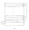
- FIG. 1 schematically shows a laminate 10 according to an embodiment of the present invention, in which 2 is an adhesion layer, 4 is a flexible layer, and 6 is a barrier layer.
- 2 is an adhesion layer
- 4 is a flexible layer
- 6 is a barrier layer.
- Each layer contains silicon atoms.
- the oxygen atom content is 10 to 35 element% in the adhesion layer as described above, 0 element% or more and less than 10 element% in the flexible layer, and more than 35 element% and less than 70 element% in the barrier layer.
- the oxygen atom content can be measured by the above method.
- the second chemical vapor deposition film may contain carbon atoms in addition to silicon atoms and oxygen atoms.
- the composition of the second chemical vapor deposition film may be such that the oxygen atom is less than 10 element%, the silicon atom is, for example, 10 to 20 element%, and the carbon atom is, for example, 20 to 35 element%. Further, it may contain, for example, 30 to 55 element% of hydrogen atoms. Nitrogen atoms may contain, for example, 10 element% or less (about 0 to 10 element%).
- the film thickness of the second chemical vapor deposition film is, for example, 5 to 1000 nm, preferably 5 to 500 nm.
- the density of the second chemical vapor deposition layer is less than 1.7 g / cm 3 (e.g., less than 1.2 g / cm 3 or more 1.7 g / cm 3) is preferable.
- oxygen atoms may be 60 to 70 element%, and silicon atoms may be 30 to 35 element%, for example. Further, it may contain a carbon atom. Further, it may contain, for example, 5 element% or less (about 0 to 5 element%) of hydrogen atoms. Nitrogen atoms may not be included.
- the film thickness of the third chemical vapor deposition film is, for example, 5 to 1000 nm, preferably 5 to 500 nm.
- the density of the third chemical vapor deposition film 1.9 g / cm 3 greater than (e.g. 1.9 g / cm 3 or less and less than 2.2 g / cm 3) is preferable.
- Table 1 shows an example of the composition of each layer of the laminate of the present invention.
- FIG. 2 schematically shows a laminate 20 according to another embodiment of the present invention.
- Reference numeral 8 denotes an organic base material such as a plastic film
- 9 denotes an inorganic base material such as Ag.
- the adhesion layer 2, the flexible layer 4, and the barrier layer 6 are laminated in this order. Further, a plurality of flexible layers 4 and barrier layers 6 are alternately laminated on each of the n layers to form the sealing film 1.
- n can be an integer from 1 to 10
- the number of flexible layers / barrier layers is preferably 6/6, 7/7, 8/8, or the like.
- Organic electroluminescent element or thin-film solar battery of the present invention includes the laminate. For this reason, it is excellent in adhesiveness and barrier property. Specifically, it is excellent in adhesiveness with a transparent conductive film or a metal film present in an organic EL element, a solar cell, etc., and the barrier film is hardly broken.
- FIG. 3 schematically shows a cross section of a thin-film photovoltaic cell 50 according to an embodiment of the present invention.
- 21 is a plastic substrate
- 22 is an ITO electrode
- 23 is a power generation layer (an organic power generation layer or an inorganic power generation layer).
- 22 is an ITO electrode
- 23 is a power generation layer (an organic power generation layer or an inorganic power generation layer).
- 24 are Ag electrodes.
- a sealing film 1 is laminated on the substrate containing organic and inorganic substances with an adhesion layer 2 interposed therebetween.
- the manufacturing method of the laminated body of the present invention is a first method in which a chemical vapor deposition film is formed on a base material by a plasma CVD method using a source gas composed of an organosilicon compound containing oxygen atoms.
- an organosilicon compound containing no oxygen atom it is preferable to use an organosilicon compound containing no oxygen atom. Further, hexamethyldisiloxane is preferred as the organosilicon compound containing oxygen atoms, and hexamethyldisilazane is preferred as the organosilicon compound not containing oxygen atoms.
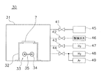
- FIG. 4 (side sectional view) and FIG. 5 (plan view) show the configuration of the film forming apparatus.
- the film forming apparatus 30 includes a vacuum chamber as a film forming chamber 31, an exhaust system 45 including a rotary pump and a turbo molecular pump, a high frequency power source 36 for generating plasma, and a flange for introducing various gases. Yes.
- the film forming chamber 31 is connected to an exhaust system 45, a film forming gas tank 46, an O 2 supply tank 47, an H 2 supply tank 48, and an Ar supply tank 49.
- the exhaust system 45 is connected to the film forming chamber 31 via the flow rate control valve 41.
- the film forming gas tank 46 is passed through the flow rate control valve 42, the O 2 supply tank 47 is passed through the flow rate control valve 43, and the H 2 supply tank 48 and the Ar supply tank 49 are passed through the flow rate control valve 44, respectively.
- 31 is connected.
- a loop antenna 33 is provided inside the film forming chamber 31.
- the loop antenna 33 is a means for generating plasma and includes an insulating tube 34 and a conductive electrode 35.
- Two insulating tubes 34 are arranged in parallel in the film forming chamber 31 so as to face each other.
- the conductive electrodes 35 are inserted into the two insulating tubes 34 and pass through the mutually opposing side walls of the film forming chamber 31 so as to have a substantially U shape in plan view as shown in FIG. Connected to a high frequency power source 36.
- the frequency of the high-frequency current is preferably 13.56 MHz.
- the plasma to be used may be CCP, ICP, barrier discharge, hollow discharge, or the like.
- the internal pressure of the film forming chamber 31 is preferably 9.9 ⁇ 10 ⁇ by the exhaust system 45. Depressurize until 5 Pa or less.
- the source gas is introduced into the film forming chamber 31 by opening the flow rate control valves 42 to 44.
- the source gas can be appropriately selected so that the chemical vapor deposition film contains silicon atoms, oxygen atoms, carbon atoms, and hydrogen atoms, and the concentration of the oxygen atoms is 10 to 35 element%.
- Specific examples of the source gas include HMSO gas alone, HMDSO + Ar / H 2 , HMDSO + O 2 , HMDSO + HMDS, HMDS + O 2, and the like. Of these, HMDSO gas alone is preferable.
- the gas introduction rate can be 3 sccm to 45 sccm.
- a high frequency current is supplied from the high frequency power source 36 to the loop antenna 33 to generate plasma around the loop antenna 33.
- the plasma power at this time can be 1 kW to 10 kW.
- a surface reaction is performed on the surface of the substrate, and a chemical vapor deposition film is formed on the substrate 7. After a predetermined time has elapsed, the introduction of gas is stopped by closing the flow control valves 42 to 44.
- a second chemical vapor deposition film (flexible layer) is formed in the same manner as described above.
- the flow control valve 44 is opened and, for example, a mixed gas of H 2 gas and Ar gas is introduced into the film forming chamber 31.
- a raw material gas such as HMDS gas is introduced by the flow rate control valve 42.
- the introduction speed of each gas at this time can be 20 sccm to 40 sccm for the mixed gas of H 2 gas and Ar gas, and 3 sccm to 20 sccm for the HMDS gas.
- a high frequency current is supplied from the high frequency power source 36 to the loop antenna 33 so that the plasma power becomes 0.1 kW to 10 kW, and plasma is generated around the loop antenna 33.
- a surface reaction is performed on the surface of the substrate, and a flexible layer 4 is formed so as to cover the adhesion layer 2 as shown in FIG. After a predetermined time has elapsed, the introduction of gas is stopped by closing the flow rate control valves 42 and 44.
- a third chemical vapor deposition film (barrier layer) is formed in the same manner as described above.
- the flow rate control valve 43 is opened and, for example, O 2 gas is introduced into the film forming chamber 31.
- a raw material gas such as HMDS gas is introduced by the flow rate control valve 42.
- the introduction speed of each gas at this time can be, for example, 20 sccm to 1000 sccm for O 2 gas and 3 sccm to 20 sccm for HMDS gas.
- a high frequency current is supplied from the high frequency power source 36 to the loop antenna 33 so that the plasma power becomes 0.1 kW to 8 kW, and plasma is generated around the loop antenna 33.
- a barrier layer 6 (silicon oxide film) is formed so as to cover the flexible layer 4 as shown in FIG. After a predetermined time has elapsed, the introduction of gas is stopped by closing the flow control valves 42 and 43.
- the adhesion layer 2 is laminated on the substrate, and on the flexible layer 4 containing silicon, a laminated body in which a silicon oxide film (barrier layer 6) is laminated is formed in seven stages.
- the HMDSO gas or the like is used as the source gas, and the adhesion layer 2 is formed on the substrate by plasma CVD, and then the flexible layer 4 is formed on the adhesion layer 2 using the HMDS gas or the HMDSO gas. Can be formed on top.
- the barrier layer 6 can be formed on the flexible layer 4 using HMDS gas, HMSO gas, or the like.
- adherence layer, the flexible layer, and the barrier layer was shown here, after forming a barrier layer on an adhesion layer, you may form a flexible layer on a barrier layer.
- a silicon nitride film may be stacked as an intermediate layer using NH 3 gas and SiH 4 gas.
- the method of the present invention does not use an etching process or the like unlike the conventional method, it does not damage a substrate such as a solar battery cell.
- the laminated body of the adhesion layer 2, the flexible layer 4, and the barrier layer 6 also has a function of protecting a substrate such as a solar battery cell from plasma energy as it is chemically vapor-grown on the substrate 7, Less damage to the device due to plasma energy.
- the formation of the adhesion layer 2 and the formation of the flexible layer 4 and the barrier layer 6 are performed in the same chamber (deposition chamber 31), the device structure can be simplified.
- Example 1 An Ag layer having a thickness of 200 nm was formed on part of the surface of the plastic film. This film was placed on the substrate fixing base in the film forming chamber so that the surface having the Ag layer was directed to the loop antenna side. Next, the internal pressure of the film formation chamber was reduced to 9.9 ⁇ 10 ⁇ 5 Pa or less by an exhaust system. After the pressure reduction in the film formation chamber was completed, HMDSO gas was introduced into the film formation chamber. The introduction speed of HMDSO gas was 3 sccm to 45 sccm.
- a high-frequency current was passed from the high-frequency power source to the loop antenna.
- the plasma power at this time was 1 kW to 10 kW.
- a surface reaction was performed on the surface of the substrate, and an adhesion layer covering a plastic film having an Ag layer was formed.
- the flow control valve was closed and the introduction of HMDSO gas was stopped.
- a flexible layer was formed using a mixed gas of HMDS gas, H 2 gas, and Ar gas.
- the introduction speed of the HMDS gas was 3 sccm to 20 sccm
- the introduction speed of the mixed gas of H 2 gas and Ar gas was 20 sccm to 40 sccm
- the plasma power was 0.1 kW to 10 kW.
- a barrier layer was formed using HMDS gas and O 2 gas in the same manner as described above.
- the introduction speed of HMDS gas was 3 sccm to 20 sccm
- the introduction speed of O 2 gas was 20 sccm to 1000 sccm
- the plasma power was 1 kW to 10 kW.
- the formation process of the flexible layer and the barrier layer was repeated 7 times. As a result, as shown in FIG. 2, a laminate in which seven layers of a laminate in which a flexible layer and a barrier layer were laminated was formed on the adhesion layer.
- the film thicknesses of one layer of the adhesion layer, the flexible layer, and the barrier layer were 128 nm, 180 nm, and 390 nm, respectively.
- the concentration of each element in the obtained laminate was determined by Rutherford backscattering spectroscopy (RBS) and hydrogen forward scattering analysis (HFS).
- RBS Rutherford backscattering spectroscopy
- HFS hydrogen forward scattering analysis
- Example 2 A laminate was obtained in the same manner as in Example 1 except that the flexible layer and the barrier layer were formed using HMDSO gas (introduction rate: 3 sccm to 30 sccm). The thickness of each layer and the concentration of each element were the same as in Example 1.
- Example 3 A laminate was obtained in the same manner as in Example 1, except that the flexible layer was formed using HMDSO gas (introduction rate: 3 sccm to 30 sccm). The thickness of each layer and the concentration of each element were the same as in Example 1.
- Example 4 A laminate was obtained in the same manner as in Example 1, except that the barrier layer was formed using HMDSO gas (introduction rate: 3 sccm to 20 sccm). The thickness of each layer and the concentration of each element were the same as in Example 1.
- Example 5 A laminate was obtained in the same manner as in Example 1 except that the adhesion layer was formed using O 2 gas (introduction rate 20 sccm to 1000 sccm) and HMDSO gas (introduction rate 3 sccm to 20 sccm).
- the thickness of each layer was the same as in Example 1.
- the oxygen element concentration of the adhesion layer was 25 element%
- the silicon atom concentration was 15 element%
- the hydrogen atom concentration was 40 element%
- the carbon atom concentration was 20 element%.
- Example 6 Example 1 is the same as Example 1 except that O 2 gas (introduction rate: 20 sccm to 1000 sccm) and HMDS gas (introduction rate: 3 sccm to 20 sccm) are used for the adhesion layer, and the plasma power is 0.1 kW to 0.5 kW. Thus, a laminate was obtained.
- the thickness of each layer was the same as in Example 1.
- the oxygen element concentration of the adhesion layer was 30 element%
- the silicon atom concentration was 22 element%
- the hydrogen atom concentration was 30 element%
- the carbon atom concentration was 18 element%.
- Example 7 Example 1 is the same as Example 1 except that O 2 gas (introduction rate: 20 sccm to 1000 sccm) and HMDS gas (introduction rate: 3 sccm to 20 sccm) are used for the adhesion layer, and the plasma power is 0.6 kW to 0.9 kW. Thus, a laminate was obtained.
- the thickness of each layer was the same as in Example 1.
- the oxygen element concentration of the adhesion layer was 35 element%
- the silicon atom concentration was 22 element%
- the hydrogen atom concentration was 28 element%
- the carbon atom concentration was 15 element%.
- Comparative Example 1 A laminate was obtained in the same manner as in Example 1 except that the adhesion layer was not formed. The thickness of each layer and the concentration of each element were the same as in Example 1.
- Comparative Example 2 Instead of forming the adhesion layer, a laminate was obtained in the same manner as in Example 1 except that the substrate was subjected to O 2 plasma treatment before vapor deposition of the flexible layer. The thickness of each layer and the concentration of each element were the same as in Example 1.
- Comparative Example 3 Instead of forming the adhesion layer, a laminate was obtained in the same manner as in Example 1 except that the substrate was subjected to Ar + H 2 plasma treatment before vapor deposition of the flexible layer. The thickness of each layer and the concentration of each element were the same as in Example 1.
- Comparative Example 4 instead of forming the adhesion layer, a laminate was obtained in the same manner as in Example 1 except that the substrate was subjected to N 2 plasma treatment before vapor deposition of the flexible layer.
- the thickness of each layer and the concentration of each element were the same as in Example 1.
- Example 1 lamination was performed in the same manner as in Example 1 except that the adhesion layer used was O 2 gas (introduction rate 20 sccm to 1000 sccm) and HMDS gas (introduction rate 3 sccm to 20 sccm), and the plasma power was changed to 1 kW to 10 kW. Got the body.
- the thickness of each layer was the same as in Example 1.
- the oxygen element concentration of the adhesion layer was 64 element%
- the silicon atom concentration was 32 element%
- the hydrogen atom concentration was 4 element%.
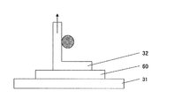
- FIG. 6 shows an outline of the tape peeling test method.
- a Kapton tape 32 having an adhesive strength of 2.7 N / 10 mm is attached to the laminate 60 of the adhesion film and the sealing film formed on the substrate 31.
- the Kapton tape is pulled at an angle of 90 degrees with respect to the substrate in the vertical direction upward at a pulling speed of 20 mm / min. In this case, the degree of peeling of the laminate 10 was observed.
- This test was evaluated according to the following criteria with a Kapton tape attached to the laminate on the Ag layer of the substrate and the laminate on the surface of the plastic film. The results are shown in Table 2.
- Barrier property evaluation method The barrier properties of the laminates of Examples 1 to 7 were evaluated.
- the barrier property was evaluated by a Ca test.
- the Ca test utilizes the fact that calcium (metal color) reacts with moisture that has passed through the gas barrier film to become calcium hydroxide (colorless and transparent). This is a method for calculating the water vapor permeability (g / m 2 / day).
- the chemical formula for the color change is shown below.
- 41 is a glass substrate
- 42 is a Ca vapor deposition film
- 70 is a film to be evaluated.
- the results are 9.0 ⁇ 10 ⁇ 5 g / m 2 / day for the laminate of Example 1, 3.0 ⁇ 10 ⁇ 4 g / m 2 / day for the laminate of Example 2, and the laminate of Example 3. It was 2.0 ⁇ 10 ⁇ 4 g / m 2 / day for the body, and 1.8 ⁇ 10 ⁇ 4 g / m 2 / day for the laminate of Example 4. Also in the laminates of Examples 5 to 7, the barrier properties were all excellent.
- the oxygen concentration can be in the range of 10 to 35 element%, and in this case, the adhesion is the highest.
- the oxygen concentration needs to be in the range of 10 to 35 element%.
- the barrier properties of the laminate including this adhesion layer were evaluated, and it was confirmed that high barrier properties were exhibited.
- Organic EL elements and solar cells that are prone to deterioration with respect to moisture and oxygen, especially organic materials (organic power generation layers, light emitting layers, plastic films (PET and PEN), etc.) and inorganic materials (transparent conductive films, metal electrodes, A barrier film with good adhesion can be formed without damaging the base material on a base material in which an inorganic power generation layer or the like is mixed and exposed.
- organic materials organic power generation layers, light emitting layers, plastic films (PET and PEN), etc.
- inorganic materials transparent conductive films, metal electrodes,
- a barrier film with good adhesion can be formed without damaging the base material on a base material in which an inorganic power generation layer or the like is mixed and exposed.
- Sealing film (flexible layer + barrier layer) 2 Adhesion layer 4 Flexible layer 6 Barrier layer 7 Base material 8 Organic substance 9 Inorganic substance 10 Laminated body (Adhesion layer + flexible layer + barrier layer) 21 Plastic substrate 22 ITO film 23 Power generation layer (organic power generation layer or inorganic power generation layer) 26 Ag electrode 27 Sealing film 50 Thin film solar cell 31 Unit 32 Kapton tape 41 Glass substrate 42 Ca vapor deposition film
Landscapes
- Chemical & Material Sciences (AREA)
- Engineering & Computer Science (AREA)
- Metallurgy (AREA)
- Organic Chemistry (AREA)
- General Chemical & Material Sciences (AREA)
- Chemical Kinetics & Catalysis (AREA)
- Materials Engineering (AREA)
- Mechanical Engineering (AREA)
- Physics & Mathematics (AREA)
- Plasma & Fusion (AREA)
- Inorganic Chemistry (AREA)
- Chemical Vapour Deposition (AREA)
- Electroluminescent Light Sources (AREA)
- Laminated Bodies (AREA)
- Ceramic Engineering (AREA)
- Microelectronics & Electronic Packaging (AREA)
Priority Applications (3)
| Application Number | Priority Date | Filing Date | Title |
|---|---|---|---|
| CN201380011749.XA CN104136657B (zh) | 2012-03-07 | 2013-01-16 | 通过等离子体cvd法形成的化学沉积膜 |
| US14/382,823 US9281420B2 (en) | 2012-03-07 | 2013-01-16 | Chemical vapor deposited film formed by plasma CVD method |
| KR1020147024084A KR102098226B1 (ko) | 2012-03-07 | 2013-01-16 | 플라즈마 cvd법에 의하여 형성된 화학 증착막 |
Applications Claiming Priority (2)
| Application Number | Priority Date | Filing Date | Title |
|---|---|---|---|
| JP2012-050960 | 2012-03-07 | ||
| JP2012050960A JP5967982B2 (ja) | 2012-03-07 | 2012-03-07 | プラズマcvd法により形成された化学蒸着膜 |
Publications (1)
| Publication Number | Publication Date |
|---|---|
| WO2013132889A1 true WO2013132889A1 (ja) | 2013-09-12 |
Family
ID=49116376
Family Applications (1)
| Application Number | Title | Priority Date | Filing Date |
|---|---|---|---|
| PCT/JP2013/050606 Ceased WO2013132889A1 (ja) | 2012-03-07 | 2013-01-16 | プラズマcvd法により形成された化学蒸着膜 |
Country Status (5)
| Country | Link |
|---|---|
| US (1) | US9281420B2 (https=) |
| JP (1) | JP5967982B2 (https=) |
| KR (1) | KR102098226B1 (https=) |
| CN (1) | CN104136657B (https=) |
| WO (1) | WO2013132889A1 (https=) |
Cited By (2)
| Publication number | Priority date | Publication date | Assignee | Title |
|---|---|---|---|---|
| US20140306211A1 (en) * | 2011-11-14 | 2014-10-16 | Konica Minolta, Inc. | Organic electroluminescent element and planar light-emitting unit |
| WO2015107702A1 (ja) * | 2014-01-15 | 2015-07-23 | コニカミノルタ株式会社 | ガスバリア性フィルム |
Families Citing this family (7)
| Publication number | Priority date | Publication date | Assignee | Title |
|---|---|---|---|---|
| CN106063374B (zh) * | 2014-02-10 | 2018-02-23 | 夏普株式会社 | 电致发光装置 |
| CN104733647B (zh) * | 2015-03-10 | 2016-08-24 | 京东方科技集团股份有限公司 | 薄膜封装方法及薄膜封装结构、显示装置 |
| CN108075040A (zh) * | 2016-11-07 | 2018-05-25 | 中国科学院苏州纳米技术与纳米仿生研究所 | 柔性oled基材及其制备方法 |
| CN109608678A (zh) * | 2018-11-07 | 2019-04-12 | 无锡泓瑞航天科技有限公司 | 一种三明治结构硅氧烷薄膜及其制备方法 |
| TWI712119B (zh) * | 2018-12-05 | 2020-12-01 | 位元奈米科技股份有限公司 | 凹槽封裝結構 |
| IT202100002966A1 (it) * | 2021-02-10 | 2022-08-10 | Sambonet Paderno Ind S P A | Copertura per prodotti argentati destinati ad entrare in contatto con alimenti |
| CN116426010A (zh) * | 2021-12-31 | 2023-07-14 | 广东聚华印刷显示技术有限公司 | 一种复合薄膜及其制备方法、显示装置 |
Citations (3)
| Publication number | Priority date | Publication date | Assignee | Title |
|---|---|---|---|---|
| JP2007221039A (ja) * | 2006-02-20 | 2007-08-30 | National Institute For Materials Science | 絶縁膜および絶縁膜材料 |
| JP2010114452A (ja) * | 2004-09-28 | 2010-05-20 | Air Products & Chemicals Inc | 多孔質の低誘電率組成物並びにそれを作製及び使用するための方法 |
| JP2010532708A (ja) * | 2007-07-06 | 2010-10-14 | シデル・パーティシペーションズ | 少なくとも3つの層を含むプラズマ堆積遮蔽コーティング、そのような1つのコーティングを得るための方法、およびそのようなコーティングでコーティングされた容器 |
Family Cites Families (10)
| Publication number | Priority date | Publication date | Assignee | Title |
|---|---|---|---|---|
| JP2526766B2 (ja) | 1992-06-15 | 1996-08-21 | 東洋製罐株式会社 | ガス遮断性積層プラスチックス材 |
| US7023010B2 (en) * | 2003-04-21 | 2006-04-04 | Nanodynamics, Inc. | Si/C superlattice useful for semiconductor devices |
| JP4432423B2 (ja) | 2003-09-25 | 2010-03-17 | 東洋製罐株式会社 | プラズマcvd法による化学蒸着膜 |
| KR101052573B1 (ko) | 2004-04-02 | 2011-07-29 | 씨제이제일제당 (주) | 균일한 함량을 갖는 과립형 동물 사료 첨가제를 제조하는 방법 및 그에 의하여 제조되는 과립형 동물 사료 첨가제 |
| US7407896B2 (en) * | 2004-04-23 | 2008-08-05 | Massachusetts Institute Of Technology | CMOS-compatible light emitting aperiodic photonic structures |
| SG121180A1 (en) * | 2004-09-28 | 2006-04-26 | Air Prod & Chem | Porous low dielectric constant compositions and methods for making and using same |
| US7256426B2 (en) * | 2005-01-19 | 2007-08-14 | Sharp Laboratories Of America, Inc. | Rare earth element-doped silicon/silicon dioxide lattice structure |
| JP4947766B2 (ja) | 2006-03-30 | 2012-06-06 | 東レエンジニアリング株式会社 | シリコン系薄膜の形成方法 |
| JP5089586B2 (ja) * | 2006-06-16 | 2012-12-05 | 東レエンジニアリング株式会社 | シリコン系薄膜及びシリコン系薄膜の形成方法 |
| TWI455338B (zh) * | 2010-02-12 | 2014-10-01 | Univ Nat Chiao Tung | 超晶格結構的太陽能電池 |
-
2012
- 2012-03-07 JP JP2012050960A patent/JP5967982B2/ja active Active
-
2013
- 2013-01-16 WO PCT/JP2013/050606 patent/WO2013132889A1/ja not_active Ceased
- 2013-01-16 CN CN201380011749.XA patent/CN104136657B/zh not_active Expired - Fee Related
- 2013-01-16 KR KR1020147024084A patent/KR102098226B1/ko active Active
- 2013-01-16 US US14/382,823 patent/US9281420B2/en active Active
Patent Citations (3)
| Publication number | Priority date | Publication date | Assignee | Title |
|---|---|---|---|---|
| JP2010114452A (ja) * | 2004-09-28 | 2010-05-20 | Air Products & Chemicals Inc | 多孔質の低誘電率組成物並びにそれを作製及び使用するための方法 |
| JP2007221039A (ja) * | 2006-02-20 | 2007-08-30 | National Institute For Materials Science | 絶縁膜および絶縁膜材料 |
| JP2010532708A (ja) * | 2007-07-06 | 2010-10-14 | シデル・パーティシペーションズ | 少なくとも3つの層を含むプラズマ堆積遮蔽コーティング、そのような1つのコーティングを得るための方法、およびそのようなコーティングでコーティングされた容器 |
Cited By (4)
| Publication number | Priority date | Publication date | Assignee | Title |
|---|---|---|---|---|
| US20140306211A1 (en) * | 2011-11-14 | 2014-10-16 | Konica Minolta, Inc. | Organic electroluminescent element and planar light-emitting unit |
| US9236583B2 (en) * | 2011-11-14 | 2016-01-12 | Konica Minolta, Inc. | Organic electroluminescent element and planar light-emitting unit |
| WO2015107702A1 (ja) * | 2014-01-15 | 2015-07-23 | コニカミノルタ株式会社 | ガスバリア性フィルム |
| JPWO2015107702A1 (ja) * | 2014-01-15 | 2017-03-23 | コニカミノルタ株式会社 | ガスバリア性フィルム |
Also Published As
| Publication number | Publication date |
|---|---|
| KR102098226B1 (ko) | 2020-04-07 |
| US20150068600A1 (en) | 2015-03-12 |
| US9281420B2 (en) | 2016-03-08 |
| KR20140136437A (ko) | 2014-11-28 |
| JP5967982B2 (ja) | 2016-08-10 |
| CN104136657B (zh) | 2017-03-08 |
| JP2013185206A (ja) | 2013-09-19 |
| CN104136657A (zh) | 2014-11-05 |
Similar Documents
| Publication | Publication Date | Title |
|---|---|---|
| JP5967982B2 (ja) | プラズマcvd法により形成された化学蒸着膜 | |
| JP2013185206A5 (https=) | ||
| EP3014675B1 (en) | Method for deposition of high-performance coatings and encapsulated electronic devices | |
| US20150132587A1 (en) | Gas barrier film and electronic device using the same | |
| JP6394600B2 (ja) | 電子デバイスおよびその製造方法 | |
| TWI700192B (zh) | 積層膜及可撓性電子裝置 | |
| CN104160062B (zh) | 含硅膜和含硅膜形成方法 | |
| KR102374497B1 (ko) | 적층 필름 및 플렉시블 전자 디바이스 | |
| JP6705170B2 (ja) | 積層フィルムおよびフレキシブル電子デバイス | |
| WO2014123201A1 (ja) | ガスバリア性フィルム、およびその製造方法 | |
| JP6657687B2 (ja) | 積層フィルムおよびフレキシブル電子デバイス | |
| JP2014100806A (ja) | ガスバリア性フィルムおよびその製造方法 | |
| CN105764845B (zh) | 功能性膜 |
Legal Events
| Date | Code | Title | Description |
|---|---|---|---|
| 121 | Ep: the epo has been informed by wipo that ep was designated in this application |
Ref document number: 13758104 Country of ref document: EP Kind code of ref document: A1 |
|
| NENP | Non-entry into the national phase |
Ref country code: DE |
|
| ENP | Entry into the national phase |
Ref document number: 20147024084 Country of ref document: KR Kind code of ref document: A |
|
| WWE | Wipo information: entry into national phase |
Ref document number: 14382823 Country of ref document: US |
|
| 122 | Ep: pct application non-entry in european phase |
Ref document number: 13758104 Country of ref document: EP Kind code of ref document: A1 |