WO2013128864A1 - 不揮発性半導体メモリー及び不揮発性半導体メモリーの製造方法 - Google Patents
不揮発性半導体メモリー及び不揮発性半導体メモリーの製造方法 Download PDFInfo
- Publication number
- WO2013128864A1 WO2013128864A1 PCT/JP2013/001031 JP2013001031W WO2013128864A1 WO 2013128864 A1 WO2013128864 A1 WO 2013128864A1 JP 2013001031 W JP2013001031 W JP 2013001031W WO 2013128864 A1 WO2013128864 A1 WO 2013128864A1
- Authority
- WO
- WIPO (PCT)
- Prior art keywords
- silicon
- oxide film
- nitride film
- silicon nitride
- silicon oxide
- Prior art date
Links
- 239000004065 semiconductor Substances 0.000 title claims abstract description 82
- 238000004519 manufacturing process Methods 0.000 title claims description 35
- 229910052581 Si3N4 Inorganic materials 0.000 claims abstract description 156
- HQVNEWCFYHHQES-UHFFFAOYSA-N silicon nitride Chemical compound N12[Si]34N5[Si]62N3[Si]51N64 HQVNEWCFYHHQES-UHFFFAOYSA-N 0.000 claims abstract description 154
- 229910052814 silicon oxide Inorganic materials 0.000 claims abstract description 140
- VYPSYNLAJGMNEJ-UHFFFAOYSA-N Silicium dioxide Chemical compound O=[Si]=O VYPSYNLAJGMNEJ-UHFFFAOYSA-N 0.000 claims abstract description 137
- XUIMIQQOPSSXEZ-UHFFFAOYSA-N Silicon Chemical compound [Si] XUIMIQQOPSSXEZ-UHFFFAOYSA-N 0.000 claims abstract description 68
- 229910052710 silicon Inorganic materials 0.000 claims abstract description 68
- 239000010703 silicon Substances 0.000 claims abstract description 68
- 239000000758 substrate Substances 0.000 claims abstract description 66
- 238000000034 method Methods 0.000 claims abstract description 34
- 229910021332 silicide Inorganic materials 0.000 claims description 21
- FVBUAEGBCNSCDD-UHFFFAOYSA-N silicide(4-) Chemical group [Si-4] FVBUAEGBCNSCDD-UHFFFAOYSA-N 0.000 claims description 19
- 238000005530 etching Methods 0.000 claims description 6
- 238000000059 patterning Methods 0.000 claims description 5
- 230000008569 process Effects 0.000 abstract description 25
- 230000015654 memory Effects 0.000 abstract description 16
- 239000010408 film Substances 0.000 description 255
- 239000010410 layer Substances 0.000 description 19
- 238000009792 diffusion process Methods 0.000 description 9
- 238000009825 accumulation Methods 0.000 description 8
- 239000010941 cobalt Substances 0.000 description 6
- 229910017052 cobalt Inorganic materials 0.000 description 6
- 238000001312 dry etching Methods 0.000 description 6
- 238000000137 annealing Methods 0.000 description 5
- 239000012535 impurity Substances 0.000 description 5
- 230000004913 activation Effects 0.000 description 4
- GUTLYIVDDKVIGB-UHFFFAOYSA-N cobalt atom Chemical compound [Co] GUTLYIVDDKVIGB-UHFFFAOYSA-N 0.000 description 4
- 230000000694 effects Effects 0.000 description 4
- 238000010438 heat treatment Methods 0.000 description 4
- 150000004767 nitrides Chemical class 0.000 description 4
- 230000008859 change Effects 0.000 description 3
- 230000007423 decrease Effects 0.000 description 3
- 239000011229 interlayer Substances 0.000 description 3
- 238000004544 sputter deposition Methods 0.000 description 3
- -1 Silicon Oxide Nitride Chemical class 0.000 description 2
- 230000004888 barrier function Effects 0.000 description 2
- 230000008901 benefit Effects 0.000 description 2
- 230000015572 biosynthetic process Effects 0.000 description 2
- 239000000470 constituent Substances 0.000 description 2
- 238000010586 diagram Methods 0.000 description 2
- 230000014759 maintenance of location Effects 0.000 description 2
- 229910021420 polycrystalline silicon Inorganic materials 0.000 description 2
- 229920005591 polysilicon Polymers 0.000 description 2
- 229910004298 SiO 2 Inorganic materials 0.000 description 1
- 229910020286 SiOxNy Inorganic materials 0.000 description 1
- 238000000277 atomic layer chemical vapour deposition Methods 0.000 description 1
- QVGXLLKOCUKJST-UHFFFAOYSA-N atomic oxygen Chemical compound [O] QVGXLLKOCUKJST-UHFFFAOYSA-N 0.000 description 1
- 238000009413 insulation Methods 0.000 description 1
- 238000005468 ion implantation Methods 0.000 description 1
- 150000002500 ions Chemical class 0.000 description 1
- 238000002955 isolation Methods 0.000 description 1
- 230000003446 memory effect Effects 0.000 description 1
- 230000006386 memory function Effects 0.000 description 1
- 229910044991 metal oxide Inorganic materials 0.000 description 1
- 230000001590 oxidative effect Effects 0.000 description 1
- 229910052760 oxygen Inorganic materials 0.000 description 1
- 239000001301 oxygen Substances 0.000 description 1
- 230000000644 propagated effect Effects 0.000 description 1
- 239000010409 thin film Substances 0.000 description 1
- 229910021341 titanium silicide Inorganic materials 0.000 description 1
- WFKWXMTUELFFGS-UHFFFAOYSA-N tungsten Chemical compound [W] WFKWXMTUELFFGS-UHFFFAOYSA-N 0.000 description 1
- 239000010937 tungsten Substances 0.000 description 1
- 229910052721 tungsten Inorganic materials 0.000 description 1
Images


Classifications
-
- H—ELECTRICITY
- H01—ELECTRIC ELEMENTS
- H01L—SEMICONDUCTOR DEVICES NOT COVERED BY CLASS H10
- H01L29/00—Semiconductor devices adapted for rectifying, amplifying, oscillating or switching, or capacitors or resistors with at least one potential-jump barrier or surface barrier, e.g. PN junction depletion layer or carrier concentration layer; Details of semiconductor bodies or of electrodes thereof ; Multistep manufacturing processes therefor
- H01L29/40—Electrodes ; Multistep manufacturing processes therefor
- H01L29/43—Electrodes ; Multistep manufacturing processes therefor characterised by the materials of which they are formed
- H01L29/49—Metal-insulator-semiconductor electrodes, e.g. gates of MOSFET
- H01L29/51—Insulating materials associated therewith
- H01L29/511—Insulating materials associated therewith with a compositional variation, e.g. multilayer structures
- H01L29/512—Insulating materials associated therewith with a compositional variation, e.g. multilayer structures the variation being parallel to the channel plane
-
- H—ELECTRICITY
- H10—SEMICONDUCTOR DEVICES; ELECTRIC SOLID-STATE DEVICES NOT OTHERWISE PROVIDED FOR
- H10B—ELECTRONIC MEMORY DEVICES
- H10B53/00—Ferroelectric RAM [FeRAM] devices comprising ferroelectric memory capacitors
- H10B53/30—Ferroelectric RAM [FeRAM] devices comprising ferroelectric memory capacitors characterised by the memory core region
-
- H—ELECTRICITY
- H01—ELECTRIC ELEMENTS
- H01L—SEMICONDUCTOR DEVICES NOT COVERED BY CLASS H10
- H01L21/00—Processes or apparatus adapted for the manufacture or treatment of semiconductor or solid state devices or of parts thereof
- H01L21/02—Manufacture or treatment of semiconductor devices or of parts thereof
- H01L21/02104—Forming layers
- H01L21/02107—Forming insulating materials on a substrate
- H01L21/02109—Forming insulating materials on a substrate characterised by the type of layer, e.g. type of material, porous/non-porous, pre-cursors, mixtures or laminates
- H01L21/02112—Forming insulating materials on a substrate characterised by the type of layer, e.g. type of material, porous/non-porous, pre-cursors, mixtures or laminates characterised by the material of the layer
- H01L21/02123—Forming insulating materials on a substrate characterised by the type of layer, e.g. type of material, porous/non-porous, pre-cursors, mixtures or laminates characterised by the material of the layer the material containing silicon
- H01L21/02164—Forming insulating materials on a substrate characterised by the type of layer, e.g. type of material, porous/non-porous, pre-cursors, mixtures or laminates characterised by the material of the layer the material containing silicon the material being a silicon oxide, e.g. SiO2
-
- H—ELECTRICITY
- H01—ELECTRIC ELEMENTS
- H01L—SEMICONDUCTOR DEVICES NOT COVERED BY CLASS H10
- H01L21/00—Processes or apparatus adapted for the manufacture or treatment of semiconductor or solid state devices or of parts thereof
- H01L21/02—Manufacture or treatment of semiconductor devices or of parts thereof
- H01L21/02104—Forming layers
- H01L21/02107—Forming insulating materials on a substrate
- H01L21/02109—Forming insulating materials on a substrate characterised by the type of layer, e.g. type of material, porous/non-porous, pre-cursors, mixtures or laminates
- H01L21/02112—Forming insulating materials on a substrate characterised by the type of layer, e.g. type of material, porous/non-porous, pre-cursors, mixtures or laminates characterised by the material of the layer
- H01L21/02123—Forming insulating materials on a substrate characterised by the type of layer, e.g. type of material, porous/non-porous, pre-cursors, mixtures or laminates characterised by the material of the layer the material containing silicon
- H01L21/0217—Forming insulating materials on a substrate characterised by the type of layer, e.g. type of material, porous/non-porous, pre-cursors, mixtures or laminates characterised by the material of the layer the material containing silicon the material being a silicon nitride not containing oxygen, e.g. SixNy or SixByNz
-
- H—ELECTRICITY
- H01—ELECTRIC ELEMENTS
- H01L—SEMICONDUCTOR DEVICES NOT COVERED BY CLASS H10
- H01L29/00—Semiconductor devices adapted for rectifying, amplifying, oscillating or switching, or capacitors or resistors with at least one potential-jump barrier or surface barrier, e.g. PN junction depletion layer or carrier concentration layer; Details of semiconductor bodies or of electrodes thereof ; Multistep manufacturing processes therefor
- H01L29/40—Electrodes ; Multistep manufacturing processes therefor
- H01L29/401—Multistep manufacturing processes
- H01L29/4011—Multistep manufacturing processes for data storage electrodes
- H01L29/40117—Multistep manufacturing processes for data storage electrodes the electrodes comprising a charge-trapping insulator
-
- H—ELECTRICITY
- H01—ELECTRIC ELEMENTS
- H01L—SEMICONDUCTOR DEVICES NOT COVERED BY CLASS H10
- H01L29/00—Semiconductor devices adapted for rectifying, amplifying, oscillating or switching, or capacitors or resistors with at least one potential-jump barrier or surface barrier, e.g. PN junction depletion layer or carrier concentration layer; Details of semiconductor bodies or of electrodes thereof ; Multistep manufacturing processes therefor
- H01L29/40—Electrodes ; Multistep manufacturing processes therefor
- H01L29/43—Electrodes ; Multistep manufacturing processes therefor characterised by the materials of which they are formed
- H01L29/49—Metal-insulator-semiconductor electrodes, e.g. gates of MOSFET
- H01L29/51—Insulating materials associated therewith
- H01L29/511—Insulating materials associated therewith with a compositional variation, e.g. multilayer structures
- H01L29/513—Insulating materials associated therewith with a compositional variation, e.g. multilayer structures the variation being perpendicular to the channel plane
-
- H—ELECTRICITY
- H01—ELECTRIC ELEMENTS
- H01L—SEMICONDUCTOR DEVICES NOT COVERED BY CLASS H10
- H01L29/00—Semiconductor devices adapted for rectifying, amplifying, oscillating or switching, or capacitors or resistors with at least one potential-jump barrier or surface barrier, e.g. PN junction depletion layer or carrier concentration layer; Details of semiconductor bodies or of electrodes thereof ; Multistep manufacturing processes therefor
- H01L29/40—Electrodes ; Multistep manufacturing processes therefor
- H01L29/43—Electrodes ; Multistep manufacturing processes therefor characterised by the materials of which they are formed
- H01L29/49—Metal-insulator-semiconductor electrodes, e.g. gates of MOSFET
- H01L29/51—Insulating materials associated therewith
- H01L29/518—Insulating materials associated therewith the insulating material containing nitrogen, e.g. nitride, oxynitride, nitrogen-doped material
-
- H—ELECTRICITY
- H01—ELECTRIC ELEMENTS
- H01L—SEMICONDUCTOR DEVICES NOT COVERED BY CLASS H10
- H01L29/00—Semiconductor devices adapted for rectifying, amplifying, oscillating or switching, or capacitors or resistors with at least one potential-jump barrier or surface barrier, e.g. PN junction depletion layer or carrier concentration layer; Details of semiconductor bodies or of electrodes thereof ; Multistep manufacturing processes therefor
- H01L29/66—Types of semiconductor device ; Multistep manufacturing processes therefor
- H01L29/66007—Multistep manufacturing processes
- H01L29/66075—Multistep manufacturing processes of devices having semiconductor bodies comprising group 14 or group 13/15 materials
- H01L29/66227—Multistep manufacturing processes of devices having semiconductor bodies comprising group 14 or group 13/15 materials the devices being controllable only by the electric current supplied or the electric potential applied, to an electrode which does not carry the current to be rectified, amplified or switched, e.g. three-terminal devices
- H01L29/66409—Unipolar field-effect transistors
- H01L29/66477—Unipolar field-effect transistors with an insulated gate, i.e. MISFET
- H01L29/66825—Unipolar field-effect transistors with an insulated gate, i.e. MISFET with a floating gate
-
- H—ELECTRICITY
- H01—ELECTRIC ELEMENTS
- H01L—SEMICONDUCTOR DEVICES NOT COVERED BY CLASS H10
- H01L29/00—Semiconductor devices adapted for rectifying, amplifying, oscillating or switching, or capacitors or resistors with at least one potential-jump barrier or surface barrier, e.g. PN junction depletion layer or carrier concentration layer; Details of semiconductor bodies or of electrodes thereof ; Multistep manufacturing processes therefor
- H01L29/66—Types of semiconductor device ; Multistep manufacturing processes therefor
- H01L29/66007—Multistep manufacturing processes
- H01L29/66075—Multistep manufacturing processes of devices having semiconductor bodies comprising group 14 or group 13/15 materials
- H01L29/66227—Multistep manufacturing processes of devices having semiconductor bodies comprising group 14 or group 13/15 materials the devices being controllable only by the electric current supplied or the electric potential applied, to an electrode which does not carry the current to be rectified, amplified or switched, e.g. three-terminal devices
- H01L29/66409—Unipolar field-effect transistors
- H01L29/66477—Unipolar field-effect transistors with an insulated gate, i.e. MISFET
- H01L29/66833—Unipolar field-effect transistors with an insulated gate, i.e. MISFET with a charge trapping gate insulator, e.g. MNOS transistors
-
- H—ELECTRICITY
- H01—ELECTRIC ELEMENTS
- H01L—SEMICONDUCTOR DEVICES NOT COVERED BY CLASS H10
- H01L29/00—Semiconductor devices adapted for rectifying, amplifying, oscillating or switching, or capacitors or resistors with at least one potential-jump barrier or surface barrier, e.g. PN junction depletion layer or carrier concentration layer; Details of semiconductor bodies or of electrodes thereof ; Multistep manufacturing processes therefor
- H01L29/66—Types of semiconductor device ; Multistep manufacturing processes therefor
- H01L29/68—Types of semiconductor device ; Multistep manufacturing processes therefor controllable by only the electric current supplied, or only the electric potential applied, to an electrode which does not carry the current to be rectified, amplified or switched
- H01L29/76—Unipolar devices, e.g. field effect transistors
- H01L29/772—Field effect transistors
- H01L29/78—Field effect transistors with field effect produced by an insulated gate
- H01L29/788—Field effect transistors with field effect produced by an insulated gate with floating gate
- H01L29/7881—Programmable transistors with only two possible levels of programmation
-
- H—ELECTRICITY
- H01—ELECTRIC ELEMENTS
- H01L—SEMICONDUCTOR DEVICES NOT COVERED BY CLASS H10
- H01L29/00—Semiconductor devices adapted for rectifying, amplifying, oscillating or switching, or capacitors or resistors with at least one potential-jump barrier or surface barrier, e.g. PN junction depletion layer or carrier concentration layer; Details of semiconductor bodies or of electrodes thereof ; Multistep manufacturing processes therefor
- H01L29/66—Types of semiconductor device ; Multistep manufacturing processes therefor
- H01L29/68—Types of semiconductor device ; Multistep manufacturing processes therefor controllable by only the electric current supplied, or only the electric potential applied, to an electrode which does not carry the current to be rectified, amplified or switched
- H01L29/76—Unipolar devices, e.g. field effect transistors
- H01L29/772—Field effect transistors
- H01L29/78—Field effect transistors with field effect produced by an insulated gate
- H01L29/792—Field effect transistors with field effect produced by an insulated gate with charge trapping gate insulator, e.g. MNOS-memory transistors
-
- H—ELECTRICITY
- H10—SEMICONDUCTOR DEVICES; ELECTRIC SOLID-STATE DEVICES NOT OTHERWISE PROVIDED FOR
- H10B—ELECTRONIC MEMORY DEVICES
- H10B53/00—Ferroelectric RAM [FeRAM] devices comprising ferroelectric memory capacitors
- H10B53/20—Ferroelectric RAM [FeRAM] devices comprising ferroelectric memory capacitors characterised by the three-dimensional arrangements, e.g. with cells on different height levels
Definitions
- the present invention relates to a nonvolatile semiconductor memory having a laminated structure of a silicon oxide film-silicon nitride film-silicon oxide film, and a method for manufacturing the nonvolatile semiconductor memory.
- EEPROM electrically erasable read-only memory
- An EEPROM is a non-volatile semiconductor memory in which stored data does not disappear even when the power is turned off.
- an EEPROM in which data can be rewritten in part or in whole is called a flash memory.
- NAND type and NOR type There are types of flash memory called NAND type and NOR type, but in either case, the memory cell itself has a similar structure, and the memory cell has a structure called a floating gate type and a charge trap type. There is something called. Both the floating gate type and the charge trap type have a MIS type transistor structure.
- a floating gate electrode is provided in a gate insulating film, and data is stored by holding electric charge in the floating gate electrode.
- the gate insulating film has a laminated structure (ONO structure) of silicon oxide film-silicon nitride film-silicon oxide film, and the vicinity of the interface between the silicon nitride film and the silicon oxide film on the silicon substrate side The data is held by changing the threshold value of the transistor by accumulating electric charge in the discrete trap existing in the transistor.
- the charge trap type includes a so-called SONOS (Silicon Oxide Nitride Oxide Semiconductor) type and MONOS (Metal Oxide Nitride Oxide Semiconductor) type.
- SONOS Silicon Oxide Nitride Oxide Semiconductor
- MONOS Metal Oxide Nitride Oxide Semiconductor
- the floating gate type was the mainstream, but in recent years, the number of cases where the charge trap type is adopted tends to increase. The reason for this is that in the case of the floating gate type, high insulation is required for the tunnel oxide film in order to trap charges in the floating gate layer.
- silicon nitride which is an insulating film, is required. Since the charges are trapped in the discrete traps of the film, there is an advantage that there is often no problem even if the insulating properties of a part of the tunnel oxide film are somewhat lowered as compared with the floating gate type.
- the thickness of the tunnel oxide film itself can be made thinner in the charge trap type, the charge trap type has a great advantage that the data write voltage can be lowered.
- Patent Document 1 provides a SiOxNy thin film having an intermediate composition of SiO 2 and Si 3 N 4 formed by atomic layer chemical vapor deposition as a trap formation layer. Is described. By forming the trap layer in this way, the trap can be formed at a desired depth with high density and good controllability, data retention characteristics, and repeated write / erase endurance can be improved, memory effect It is described that the difference between the threshold voltages can be large, and this is advantageous for multi-leveling.
- the present invention has been made to solve at least one of the above-described problems or problems, and can be realized as the following application examples or embodiments.
- the nonvolatile semiconductor memory according to this application example includes a silicon substrate, a first silicon oxide film, a second silicon oxide film, a first silicon nitride film, and a second silicon nitride film,
- the first silicon oxide film is stacked on the silicon substrate
- the first silicon nitride film is stacked on the first silicon oxide film
- the second silicon oxide film is stacked on the first silicon oxide film.
- the second silicon nitride film is laminated such that the first portion is in contact with the first silicon nitride film and the second portion is in contact with the silicon substrate. It is characterized by.
- the charge holding portion of the nonvolatile semiconductor memory is configured by the first silicon oxide film, the first silicon nitride film, and the second silicon oxide film stacked on the silicon substrate (ONO structure). ),
- the second silicon nitride film is in contact with the first silicon nitride film and the silicon substrate, so that excess charges trapped in the ONO structure in a predetermined process at the time of manufacturing are processed in another predetermined process.
- the first silicon nitride film may be in a state of capturing charges, and the manufacturing may be completed while maintaining the state of capturing charges.
- the amount of charge that remains trapped in the first silicon nitride film may affect the operation of the nonvolatile semiconductor memory.
- the threshold voltage in the write operation as the memory becomes higher.
- the threshold voltage is higher, it is conceivable that the amount of charge newly trapped in the first silicon nitride film is smaller when a write operation is performed as a nonvolatile semiconductor memory.
- the non-volatile semiconductor memory in which the manufacturing process is completed while a large amount of charge is captured by the first silicon nitride film becomes a non-volatile semiconductor memory unsuitable for high-speed and low-voltage operation.
- the threshold voltage of the memory varies from the design value, there is a limit to the change / adjustment of the impurity concentration in the channel portion that accompanies the variation in threshold voltage.
- the first portion of the second silicon nitride film is in contact with the first silicon nitride film
- the second portion of the second silicon nitride film is in contact with the silicon substrate.
- the charge trapped in the first silicon nitride film in the process can be diffused to the silicon substrate through the second silicon nitride film in another predetermined process after the predetermined process.
- the amount of charges remaining trapped in the first silicon nitride film can be reduced, and the operation of the nonvolatile semiconductor memory can be speeded up and the voltage can be lowered.
- the nonvolatile semiconductor memory according to this application example includes a silicon substrate, a first silicon oxide film, a second silicon oxide film, a third silicon oxide film, a first silicon nitride film, and a second silicon oxide film.
- the silicon oxide film is stacked on the first silicon nitride film, the thickness of the third silicon oxide film is smaller than the thickness of the first silicon oxide film, and the second silicon nitride film is The first portion is in contact with the first silicon nitride film, and the second portion is in contact with the silicon substrate through the third silicon oxide film.
- the charge holding portion of the nonvolatile semiconductor memory is configured by the first silicon oxide film, the first silicon nitride film, and the second silicon oxide film stacked on the silicon substrate (ONO structure). ),
- the second silicon nitride film is in contact with the first silicon nitride film and is in contact with the silicon substrate through the third silicon oxide film, so that it is captured in the ONO structure in a predetermined process during manufacturing.
- the extra charge thus generated can be diffused through the second silicon nitride film and the third silicon oxide film in another predetermined process, and the influence of the extra charge on the threshold voltage can be reduced. As a result, the memory operation can be speeded up and the voltage can be reduced.
- reducing the charge trapped in the first silicon nitride film during the manufacturing process has the effect of speeding up and lowering the operation of the nonvolatile semiconductor memory. Since the third silicon oxide film is thinner than the first silicon oxide film, the second silicon nitride film and the third silicon oxide film pass through the first silicon oxide film. It is possible to diffuse the charges trapped in the first silicon nitride film more easily.
- a silicide region is further included in the silicon substrate, and the silicide region is in contact with a second portion of the second silicon nitride film.
- the second silicon nitride film since the second silicon nitride film is in contact with the silicide region, charges from the second silicon nitride film can be more efficiently diffused into the silicon substrate.
- the silicide region may be in contact with the second silicon nitride film via the third silicon oxide film.
- the nonvolatile semiconductor memory according to the application example further includes a first electrode on the second silicon oxide film, and a third portion of the second silicon nitride film is in contact with the first electrode. It is preferable.
- the charges trapped in the first silicon nitride film during the manufacturing process are transferred via the second silicon nitride film. Can be diffused to one electrode. Thereby, the charge can be diffused to the silicon substrate and the charge can be diffused to the first electrode, and the charge captured by the first silicon nitride film can be diffused more efficiently.
- the third silicon oxide film has a thickness of 22 mm or less.
- the charge from the second silicon nitride film can be more efficiently diffused into the silicon substrate by setting the thickness of the third silicon oxide film to 22 mm or less.
- the second silicon nitride film has a thickness of 45 mm or more.
- the charge of the first silicon nitride film can be more efficiently propagated to the second silicon nitride film.
- the method for manufacturing a nonvolatile semiconductor memory includes a first step of forming a first silicon oxide film on a silicon substrate, and a first silicon nitride film on the first silicon oxide film.
- a second step of forming a film; a third step of forming a second silicon oxide film on the first silicon nitride film; and the first silicon oxide film and the first silicon A fourth step of patterning the nitride film and the second silicon oxide film into a predetermined shape; and a fifth step of forming a second silicon nitride film after the fourth step,
- the first silicon nitride film and the silicon substrate are exposed, and in the fifth step, the first silicon nitride film and the second silicon nitride film are in contact with each other. .
- the first silicon nitride film and the silicon substrate are exposed by the patterning in the fourth step, and the second silicon nitride film is formed in the fifth step after the fourth step.
- the second silicon nitride film can be in contact with the first silicon nitride film and can be in contact with the silicon substrate.
- a third silicon oxide film is formed in a region where the silicon substrate is exposed. It may be formed.
- the second silicon nitride film by forming the second silicon nitride film in the fifth step, the second silicon nitride film can be brought into contact with the first silicon nitride film, and the silicon substrate Can be in contact with each other via a third silicon oxide film.
- the third silicon oxide film may be formed by heating in an oxygen atmosphere.
- a naturally-occurring silicon oxide film formed by oxidizing the silicon substrate by exposure to air or the like is used as the third silicon oxide film.
- An oxide film may be used.
- the method for manufacturing a nonvolatile semiconductor memory includes a first step of forming a first silicon oxide film on a silicon substrate, and a first silicon nitride film on the first silicon oxide film.
- a second step of forming a film; a third step of forming a second silicon oxide film on the first silicon nitride film; and the first silicon oxide film and the first silicon A fourth step of patterning the nitride film and the second silicon oxide film into a predetermined shape; and a fifth step of forming a second silicon nitride film after the fourth step,
- step 4 the first silicon nitride film is exposed, and a third silicon oxide film having a thickness smaller than that of the first silicon oxide film is formed by etching the first silicon oxide film.
- the first series Characterized in that said the emissions nitride film second silicon nitride film in contact.
- the second silicon nitride film can be brought into contact with the first silicon nitride film, and the silicon substrate Can be in contact with each other via a third silicon oxide film.
- FIG. 1 is a schematic cross-sectional view of a nonvolatile semiconductor memory according to a first embodiment.
- the graph which showed the characteristic of the 3rd silicon oxide film The schematic diagram which shows a part of manufacturing process.
- the schematic diagram which shows a part of manufacturing process. 1 is a schematic cross-sectional view of a conventional nonvolatile semiconductor memory.
- FIG. 1 shows a cross-sectional view of a nonvolatile semiconductor memory 100 to which the present invention is applied.
- the nonvolatile semiconductor memory 100 is formed using a silicon substrate 12, and includes a first electrode 10, a sidewall 11, a source region / drain region 13, a silicide region 14, a silicide layer 15, a first silicon oxide film 20, and a first silicon.
- a nitride film 21, a second silicon oxide film 22, and a second silicon nitride film 23 are provided.
- a polysilicon film is used as the first electrode 10
- a silicon oxide film is used as the sidewall 11, for example.
- the source region / drain region 13 and the silicide region 14 are regions formed in the silicon substrate 12.
- the trap layer for the memory function has an ONO structure including the first silicon oxide film 20, the first silicon nitride film 21, and the second silicon oxide film 22.
- the second silicon nitride film 23 is in contact with the first silicon nitride film 21 and the silicon substrate 12.
- the silicon substrate 12 is described as including the source region / drain region 13 and the silicide region 14.
- FIG. 9 shows a cross-sectional view of a conventional nonvolatile semiconductor memory 900.
- the nonvolatile semiconductor memory 900 is different from the nonvolatile semiconductor memory 100 to which the present invention is applied in that the second silicon nitride film 23 is not provided.
- a silicon oxide film is generally used as the sidewall 11, and in this case, the side surface of the first silicon nitride film is covered with the silicon oxide film.
- the nonvolatile semiconductor memories 100 and 900 processing using plasma such as etching and sputtering is frequently used.
- the first silicon oxide film 20, the first silicon nitride film 21, and the second silicon oxide film 22 are used.
- Charges derived from plasma are injected and held in the ONO structure (trap layer) composed of Such a phenomenon is called process charge in the present application.
- the process charge is generated, in the conventional nonvolatile semiconductor memory 900, it is difficult to diffuse the charge due to the process charge because the insulating property of the silicon oxide film is high.
- the manufacturing process may be completed while a large amount of charge is trapped in the trap layer, resulting in a nonvolatile semiconductor memory that is not suitable for high-speed and low-voltage operation.
- the threshold voltage of the memory varies from the design value, there is a limit to the change / adjustment of the impurity concentration in the channel portion that accompanies the variation in threshold voltage.
- a second silicon nitride film 23 is newly provided in the conventional nonvolatile semiconductor memory 900.
- the second silicon nitride film 23 is in contact with the side surface of the first silicon nitride film 21 and the silicon substrate 12.
- the silicon nitride film has a lower insulating property than the silicon oxide film. Therefore, it becomes possible to diffuse the charge due to the process charge held in the trap layer to the silicon substrate 12 through the second silicon nitride film 23. Charge diffusion is accelerated by heat treatment.
- heat treatment heat treatment conventionally performed in the memory manufacturing process such as impurity activation or silicidation may be used, or a dedicated process may be provided.
- the second silicon nitride film 23 may be an insulating film having a lower insulating property than the silicon oxide film. For example, a silicon oxynitride film may be used.
- FIG. 5 is a graph showing the relationship between the thickness of the second silicon nitride film and the threshold voltage of the nonvolatile semiconductor memories 100 and 900.
- electrons are accumulated in the trap layer by the process charge, and the threshold voltage rises.
- the threshold voltage is 1.0V.
- the electrons accumulated in the trap layer are diffused and the threshold voltage is lowered as the thickness of the second silicon nitride film is increased. To do.
- the thickness of the second silicon nitride film is 45 mm or more, the threshold voltage decreases to around 0.6 V and becomes stable, which is particularly preferable.
- the film thickness dependence of the threshold voltage is the same in the second to fourth embodiments described later.
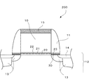
- FIG. 2 shows a cross-sectional view of a nonvolatile semiconductor memory 200 to which the present invention is applied.
- the nonvolatile semiconductor memory 200 is obtained by adding a third silicon oxide film 30 to the constituent elements of the nonvolatile semiconductor memory 100.
- the second silicon nitride film 23 is in contact with the silicon substrate 12 through the third silicon oxide film 30.
- the third silicon oxide film 30 is formed thinner than the first silicon oxide film 20. Thereby, even if the first silicon oxide film 20 becomes a barrier against diffusing the charge of the first silicon nitride film 21, the charge can be diffused through the third silicon oxide film 30.
- FIG. 6 is a graph showing the relationship between the film thickness of the third silicon oxide film and the threshold voltage of the nonvolatile semiconductor memory 200.
- electrons are accumulated in the trap layer by the process charge, and the threshold voltage rises.
- the threshold voltage rises.
- a thickness of the third silicon oxide film of 22 mm or more is particularly preferable because the threshold voltage is reduced to around 0.5 V and becomes stable.
- the film thickness dependence of the threshold voltage is the same in the fourth embodiment described later.
- the third silicon oxide film 30 may be intentionally formed, or may be naturally formed in a process before the second silicon nitride film 23 is formed.
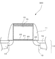
- FIG. 3 shows a cross-sectional view of a nonvolatile semiconductor memory 300 to which the present invention is applied.
- the nonvolatile semiconductor memory 300 includes a second silicon nitride film 24 that is in contact with the silicon substrate 12 and the first electrode 10.
- the sidewall 11 is formed so as to cover the second silicon nitride film 24.
- the thickness of the second silicon nitride film 24 is preferably 45 mm or more.
- the charges trapped in the first silicon nitride film 21 are diffused to the first electrode 10 and the silicon substrate 12 through the second silicon nitride film 24, and the efficiency is higher than the case of diffusing only to the silicon substrate 12. Get better. Thereby, the freedom degree with respect to the setting of the temperature of heat processing and the setting of time can be raised.
- FIG. 4 shows a cross-sectional view of a nonvolatile semiconductor memory 400 to which the present invention is applied.
- the nonvolatile semiconductor memory 400 is obtained by adding a third silicon oxide film 31 to the constituent elements of the nonvolatile semiconductor memory 300.
- the second silicon nitride film 24 is in contact with the silicon substrate 12 through the third silicon oxide film 31.
- the thickness of the third silicon oxide film 31 is formed thinner than the thickness of the first silicon oxide film 20. Thereby, even if the first silicon oxide film 20 becomes a barrier against diffusing the charge of the first silicon nitride film 21, the charge can be diffused through the third silicon oxide film 31.
- the thickness of the third silicon oxide film 31 is preferably 22 mm or less.
- the third silicon oxide film 31 may be intentionally formed, or may be naturally formed in a step before the second silicon nitride film 24 is formed.
- the silicide region 14 is formed in the silicon substrate 12 in any of the above-described nonvolatile semiconductor memories 100, 200, 300, and 400. Since the silicide region 14 has a lower electrical resistance than other portions of the silicon substrate 12, the formation of the silicide region 14 is preferable because it increases the efficiency of the process of diffusing the charge of the process charge into the substrate.
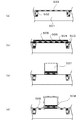
- FIG. 7 and 8 are schematic views of cross-sectional views of the element in the manufacturing process. In the figure, only the nonvolatile semiconductor memory portion is shown, and other types of elements are formed at the same time. A region where the nonvolatile semiconductor memory is formed is called an ONO region.
- FIG. 7A shows a state in which a dummy oxide film 503 is formed after the STI (Shallow Trench Isolation) 502 is formed on the silicon substrate 501.
- the dummy oxide film 503 is used to eliminate the influence on the substrate when the ONO is removed from regions other than the ONO region when forming the ONO structure. Thereafter, the dummy oxide film 503 in the ONO region is removed, and an ONO structure is stacked.
- FIG. 7B shows a state where the ONO structure formed on the dummy oxide film 503 is removed after the ONO structure is stacked. Thereafter, the remaining dummy oxide film 503 is removed, and a gate oxide film of a transistor other than the ONO region is formed.
- the ONO structure in the ONO region includes a first silicon oxide film 504, a first silicon nitride film 505, and a second silicon oxide film 506.
- a first gate electrode 507 having a predetermined shape is formed by dry etching (FIG. 7C).
- the dry etching step is a step caused by process charge (hereinafter referred to as a charge accumulation step).
- ion implantation corresponding to the device is performed to form an impurity region 509, and then a second silicon nitride film 508 is formed (FIG. 7D).
- a silicon oxide film is formed to form sidewalls, and sidewalls 510 are formed by anisotropic etching.
- This anisotropic etching is also a charge accumulation process. Since the silicon nitride film is a highly stressed film, if a sidewall is formed only with the silicon nitride film, a problem due to stress may occur. Therefore, it is preferable that the sidewall 510 has a stacked structure with not only a silicon nitride film but also a silicon oxide film.
- ions for forming the source region / drain region are implanted, and activation annealing is performed. (FIG. 8- (e)).
- the activation annealing is a step of diffusing a process charge (hereinafter referred to as a charge diffusion step).
- the charges accumulated in the first silicon nitride film 505 and the second silicon nitride film 508 are diffused into the silicon substrate 501 and the first gate electrode 507 by the activation annealing.
- Co (cobalt) is sputtered and annealed to form a cobalt silicide region 511 and a cobalt silicide layer 515.
- the sputtering is a charge accumulation process
- the annealing is a charge diffusion process. (FIG. 8- (f)).
- an interlayer insulating film 512 is formed, and a contact hole 513 is formed by dry etching.
- the dry etching is a charge accumulation process, and the process of forming a wiring 514 by forming a film of tungsten and the like after the dry etching is a charge diffusion process (FIG. 8- (g)).
- the charge accumulation process and the charge diffusion process are repeated. It is.
- the charges accumulated in the ONO structure (trap layer) composed of the first silicon oxide film 504, the first silicon nitride film 505, and the second silicon oxide film 506 in the charge accumulation process are transferred to the silicon substrate 501 and the first silicon oxide film 504 in the charge diffusion process.
- 1 gate electrode 507 can be diffused. It is preferable to provide a charge diffusion step after the final charge accumulation step so that the trap layer does not remain trapped when all the steps necessary for manufacturing are completed. More preferably, the final step is a charge diffusion step. This makes it possible to manufacture a nonvolatile semiconductor memory that eliminates the negative effects of process charge.
- a step of forming a third silicon oxide film may be added before the second silicon nitride film 508 is formed.
- the third silicon oxide film is intentionally formed by processing the silicon substrate so as not to expose the silicon substrate. It may be formed.
- the manufacturing process is configured in consideration of using a silicon oxide film naturally formed between the silicon substrate and the second silicon nitride film as the third silicon oxide film in the manufacturing process. May be.
- the manufacturing method in the case of the nonvolatile semiconductor memory 300 or 400 has been described.
- the manufacturing process is different because the shape of the second silicon nitride film is different. come.
- the charge diffusion step exists after the charge accumulation step, it is possible to obtain the same effect as the effect in the manufacturing method described in the present embodiment.
- SYMBOLS 10 ... 1st electrode, 11 ... Side wall, 12 ... Silicon substrate, 13 ... Source / drain region, 14 ... Silicide region, 15 ... Silicide layer, 20 ... 1st silicon oxide film, 21 ... 1st silicon nitride film, 22 2nd silicon oxide film, 23 ... 2nd silicon nitride film, 24 ... 2nd silicon nitride film, 30 ... 3rd silicon oxide film, 31 ... 3rd silicon oxide film, 100 ... Nonvolatile semiconductor memory, 200 ... Nonvolatile Semiconductor memory 300 ... Non-volatile semiconductor memory 400 ... Non-volatile semiconductor memory 501 ... Silicon substrate 502 ... STI 503 ...
- Dummy oxide film 504 ... First silicon oxide film 505 ... First silicon nitride film 506 ... Second silicon oxide film, 507... First gate electrode, 508. Second silicon nitride film, 509... Impurity region, 510. Doworu, 511 ... cobalt silicide region 512 ... interlayer insulating film, 513 ... contact hole, 514 ... wire, 515 ... cobalt silicide layer, 900 ... non-volatile semiconductor memory.
Priority Applications (3)
| Application Number | Priority Date | Filing Date | Title |
|---|---|---|---|
| CN201380010880.4A CN104137239B (zh) | 2012-02-28 | 2013-02-22 | 非易失性半导体存储器以及非易失性半导体存储器的制造方法 |
| US14/377,278 US9461138B2 (en) | 2012-02-28 | 2013-02-22 | Non-volatile semiconductor memory with nitride sidewall contacting nitride layer of ONO gate stack and methods for producing the same |
| KR1020147026353A KR101618160B1 (ko) | 2012-02-28 | 2013-02-22 | 불휘발성 반도체 메모리 및 불휘발성 반도체 메모리의 제조 방법 |
Applications Claiming Priority (2)
| Application Number | Priority Date | Filing Date | Title |
|---|---|---|---|
| JP2012-041221 | 2012-02-28 | ||
| JP2012041221A JP5998521B2 (ja) | 2012-02-28 | 2012-02-28 | 不揮発性半導体メモリー及び不揮発性半導体メモリーの製造方法 |
Publications (1)
| Publication Number | Publication Date |
|---|---|
| WO2013128864A1 true WO2013128864A1 (ja) | 2013-09-06 |
Family
ID=49082077
Family Applications (1)
| Application Number | Title | Priority Date | Filing Date |
|---|---|---|---|
| PCT/JP2013/001031 WO2013128864A1 (ja) | 2012-02-28 | 2013-02-22 | 不揮発性半導体メモリー及び不揮発性半導体メモリーの製造方法 |
Country Status (6)
| Country | Link |
|---|---|
| US (1) | US9461138B2 (ko) |
| JP (1) | JP5998521B2 (ko) |
| KR (1) | KR101618160B1 (ko) |
| CN (1) | CN104137239B (ko) |
| TW (1) | TWI609480B (ko) |
| WO (1) | WO2013128864A1 (ko) |
Families Citing this family (20)
| Publication number | Priority date | Publication date | Assignee | Title |
|---|---|---|---|---|
| JP6880595B2 (ja) * | 2016-08-10 | 2021-06-02 | セイコーエプソン株式会社 | 半導体装置及びその製造方法 |
| US10777566B2 (en) | 2017-11-10 | 2020-09-15 | Macronix International Co., Ltd. | 3D array arranged for memory and in-memory sum-of-products operations |
| US10719296B2 (en) | 2018-01-17 | 2020-07-21 | Macronix International Co., Ltd. | Sum-of-products accelerator array |
| US10957392B2 (en) | 2018-01-17 | 2021-03-23 | Macronix International Co., Ltd. | 2D and 3D sum-of-products array for neuromorphic computing system |
| US20190244662A1 (en) * | 2018-02-02 | 2019-08-08 | Macronix International Co., Ltd. | Sum-of-products array for neuromorphic computing system |
| JP6976190B2 (ja) * | 2018-02-20 | 2021-12-08 | キオクシア株式会社 | 記憶装置 |
| US10635398B2 (en) | 2018-03-15 | 2020-04-28 | Macronix International Co., Ltd. | Voltage sensing type of matrix multiplication method for neuromorphic computing system |
| US11138497B2 (en) | 2018-07-17 | 2021-10-05 | Macronix International Co., Ltd | In-memory computing devices for neural networks |
| US11636325B2 (en) | 2018-10-24 | 2023-04-25 | Macronix International Co., Ltd. | In-memory data pooling for machine learning |
| US10672469B1 (en) | 2018-11-30 | 2020-06-02 | Macronix International Co., Ltd. | In-memory convolution for machine learning |
| US11562229B2 (en) | 2018-11-30 | 2023-01-24 | Macronix International Co., Ltd. | Convolution accelerator using in-memory computation |
| US11934480B2 (en) | 2018-12-18 | 2024-03-19 | Macronix International Co., Ltd. | NAND block architecture for in-memory multiply-and-accumulate operations |
| US11119674B2 (en) | 2019-02-19 | 2021-09-14 | Macronix International Co., Ltd. | Memory devices and methods for operating the same |
| US10783963B1 (en) | 2019-03-08 | 2020-09-22 | Macronix International Co., Ltd. | In-memory computation device with inter-page and intra-page data circuits |
| US11132176B2 (en) | 2019-03-20 | 2021-09-28 | Macronix International Co., Ltd. | Non-volatile computing method in flash memory |
| US10910393B2 (en) | 2019-04-25 | 2021-02-02 | Macronix International Co., Ltd. | 3D NOR memory having vertical source and drain structures |
| JP2021061450A (ja) * | 2021-01-20 | 2021-04-15 | セイコーエプソン株式会社 | 半導体装置及びその製造方法 |
| US11737274B2 (en) | 2021-02-08 | 2023-08-22 | Macronix International Co., Ltd. | Curved channel 3D memory device |
| US11916011B2 (en) | 2021-04-14 | 2024-02-27 | Macronix International Co., Ltd. | 3D virtual ground memory and manufacturing methods for same |
| US11710519B2 (en) | 2021-07-06 | 2023-07-25 | Macronix International Co., Ltd. | High density memory with reference memory using grouped cells and corresponding operations |
Citations (6)
| Publication number | Priority date | Publication date | Assignee | Title |
|---|---|---|---|---|
| JP2001326288A (ja) * | 2000-03-10 | 2001-11-22 | Fujitsu Ltd | 不揮発性半導体メモリの製造方法およびそれにより製造される不揮発性半導体メモリ |
| JP2004165553A (ja) * | 2002-11-15 | 2004-06-10 | Toshiba Corp | 半導体記憶装置 |
| WO2006080081A1 (ja) * | 2005-01-28 | 2006-08-03 | Spansion Llc | 不揮発性メモリ及びその制御方法 |
| JP2006269697A (ja) * | 2005-03-23 | 2006-10-05 | Genusion:Kk | 不揮発性半導体記憶装置 |
| JP2007005699A (ja) * | 2005-06-27 | 2007-01-11 | Matsushita Electric Ind Co Ltd | 不揮発性半導体記憶装置及びその製造方法 |
| JP2009071325A (ja) * | 2008-11-25 | 2009-04-02 | Renesas Technology Corp | 半導体装置の製造方法及び半導体装置 |
Family Cites Families (17)
| Publication number | Priority date | Publication date | Assignee | Title |
|---|---|---|---|---|
| JPH07226502A (ja) | 1994-02-14 | 1995-08-22 | Sony Corp | Mosトランジスタ及びその製造方法 |
| JP3240999B2 (ja) | 1998-08-04 | 2001-12-25 | 日本電気株式会社 | 半導体記憶装置及びその製造方法 |
| US6573132B1 (en) | 1999-03-25 | 2003-06-03 | Matsushita Electric Industrial Co., Ltd. | Method for fabricating a semiconductor device having contacts self-aligned with a gate electrode thereof |
| JP3482171B2 (ja) | 1999-03-25 | 2003-12-22 | 松下電器産業株式会社 | 半導体装置及びその製造方法 |
| JP3961211B2 (ja) | 2000-10-31 | 2007-08-22 | 株式会社東芝 | 半導体装置の製造方法 |
| JP2002222876A (ja) | 2001-01-25 | 2002-08-09 | Sony Corp | 不揮発性半導体記憶素子及びその製造方法 |
| JP3641596B2 (ja) | 2001-05-09 | 2005-04-20 | 株式会社東芝 | 半導体記憶装置及びその製造方法 |
| US6555865B2 (en) | 2001-07-10 | 2003-04-29 | Samsung Electronics Co. Ltd. | Nonvolatile semiconductor memory device with a multi-layer sidewall spacer structure and method for manufacturing the same |
| JP2003264247A (ja) * | 2002-03-11 | 2003-09-19 | Toshiba Corp | 不揮発性半導体記憶装置及びその製造方法 |
| KR100463184B1 (ko) | 2003-01-30 | 2004-12-23 | 아남반도체 주식회사 | 비휘발성 메모리 장치 제조 방법 |
| KR100546692B1 (ko) * | 2004-05-03 | 2006-01-26 | 동부아남반도체 주식회사 | 플래시 메모리 소자의 제조 방법 |
| JP2006032541A (ja) | 2004-07-14 | 2006-02-02 | Renesas Technology Corp | 半導体装置 |
| KR100642898B1 (ko) | 2004-07-21 | 2006-11-03 | 에스티마이크로일렉트로닉스 엔.브이. | 반도체 장치의 트랜지스터 및 그 제조방법 |
| US7405441B2 (en) * | 2005-03-11 | 2008-07-29 | Infineon Technology Ag | Semiconductor memory |
| JP2008218727A (ja) | 2007-03-05 | 2008-09-18 | Renesas Technology Corp | 半導体装置とその製造方法 |
| US8471328B2 (en) * | 2010-07-26 | 2013-06-25 | United Microelectronics Corp. | Non-volatile memory and manufacturing method thereof |
| US8629025B2 (en) * | 2012-02-23 | 2014-01-14 | United Microelectronics Corp. | Semiconductor device and method for fabricating semiconductor device |
-
2012
- 2012-02-28 JP JP2012041221A patent/JP5998521B2/ja active Active
-
2013
- 2013-02-22 US US14/377,278 patent/US9461138B2/en active Active
- 2013-02-22 CN CN201380010880.4A patent/CN104137239B/zh active Active
- 2013-02-22 WO PCT/JP2013/001031 patent/WO2013128864A1/ja active Application Filing
- 2013-02-22 KR KR1020147026353A patent/KR101618160B1/ko active IP Right Grant
- 2013-02-23 TW TW102106457A patent/TWI609480B/zh active
Patent Citations (6)
| Publication number | Priority date | Publication date | Assignee | Title |
|---|---|---|---|---|
| JP2001326288A (ja) * | 2000-03-10 | 2001-11-22 | Fujitsu Ltd | 不揮発性半導体メモリの製造方法およびそれにより製造される不揮発性半導体メモリ |
| JP2004165553A (ja) * | 2002-11-15 | 2004-06-10 | Toshiba Corp | 半導体記憶装置 |
| WO2006080081A1 (ja) * | 2005-01-28 | 2006-08-03 | Spansion Llc | 不揮発性メモリ及びその制御方法 |
| JP2006269697A (ja) * | 2005-03-23 | 2006-10-05 | Genusion:Kk | 不揮発性半導体記憶装置 |
| JP2007005699A (ja) * | 2005-06-27 | 2007-01-11 | Matsushita Electric Ind Co Ltd | 不揮発性半導体記憶装置及びその製造方法 |
| JP2009071325A (ja) * | 2008-11-25 | 2009-04-02 | Renesas Technology Corp | 半導体装置の製造方法及び半導体装置 |
Also Published As
| Publication number | Publication date |
|---|---|
| KR101618160B1 (ko) | 2016-05-04 |
| KR20140136000A (ko) | 2014-11-27 |
| US9461138B2 (en) | 2016-10-04 |
| US20150008500A1 (en) | 2015-01-08 |
| JP2013179122A (ja) | 2013-09-09 |
| TW201347149A (zh) | 2013-11-16 |
| JP5998521B2 (ja) | 2016-09-28 |
| CN104137239B (zh) | 2018-01-12 |
| CN104137239A (zh) | 2014-11-05 |
| TWI609480B (zh) | 2017-12-21 |
Similar Documents
| Publication | Publication Date | Title |
|---|---|---|
| JP5998521B2 (ja) | 不揮発性半導体メモリー及び不揮発性半導体メモリーの製造方法 | |
| JP4885420B2 (ja) | Sonos型装置の分離を改善するためのono形成中のソース・ドレイン注入 | |
| JP2012114269A (ja) | 半導体装置および半導体装置の製造方法 | |
| JP2008504681A (ja) | ナノクラスタ電荷蓄積デバイスの形成方法 | |
| US8592892B2 (en) | Nonvolatile semiconductor memory device and method for manufacturing the same | |
| TW201030945A (en) | Nonvolatile memory cell and method for fabricating the same | |
| WO2008112370A1 (en) | Electronic device including channel regions lying at different elevations and processes of forming the same | |
| US20100270604A1 (en) | Non-Volatile Memories and Methods of Fabrication Thereof | |
| JP2010087046A (ja) | 不揮発性半導体装置及び不揮発性半導体装置の製造方法 | |
| JP2006041510A (ja) | 半導体素子のdram及びその製造方法 | |
| KR100606928B1 (ko) | 비휘발성 메모리 장치 및 그 제조방법 | |
| CN108140564B (zh) | 在存储器单元中形成多晶硅侧壁氧化物间隔件的方法 | |
| JP5937172B2 (ja) | 半導体装置および半導体装置の製造方法 | |
| JP5421549B2 (ja) | 半導体装置の製造方法及び半導体装置 | |
| KR100806039B1 (ko) | 플래시 메모리 소자 및 이의 제조 방법 | |
| CN106024852B (zh) | 用于制造半导体器件的方法 | |
| CN110729301A (zh) | 半导体器件及其制造方法 | |
| US11978772B2 (en) | Method of manufacturing semiconductor device | |
| KR20080104477A (ko) | 반도체 소자 및 그의 제조 방법 | |
| JP2005197684A (ja) | 半導体装置 | |
| US20090218615A1 (en) | Semiconductor device and method of manufacturing the same | |
| JP5363004B2 (ja) | 半導体装置の製造方法 | |
| JPH1167940A (ja) | 不揮発性半導体記憶装置及びその製造方法 | |
| KR100668727B1 (ko) | 플래쉬 메모리 소자의 제조방법 | |
| JP2010129594A (ja) | 半導体記憶装置及びその製造方法 |
Legal Events
| Date | Code | Title | Description |
|---|---|---|---|
| 121 | Ep: the epo has been informed by wipo that ep was designated in this application |
Ref document number: 13755099 Country of ref document: EP Kind code of ref document: A1 |
|
| WWE | Wipo information: entry into national phase |
Ref document number: 14377278 Country of ref document: US |
|
| NENP | Non-entry into the national phase |
Ref country code: DE |
|
| ENP | Entry into the national phase |
Ref document number: 20147026353 Country of ref document: KR Kind code of ref document: A |
|
| 122 | Ep: pct application non-entry in european phase |
Ref document number: 13755099 Country of ref document: EP Kind code of ref document: A1 |