WO2012157223A1 - 横型半導体装置 - Google Patents
横型半導体装置 Download PDFInfo
- Publication number
- WO2012157223A1 WO2012157223A1 PCT/JP2012/003065 JP2012003065W WO2012157223A1 WO 2012157223 A1 WO2012157223 A1 WO 2012157223A1 JP 2012003065 W JP2012003065 W JP 2012003065W WO 2012157223 A1 WO2012157223 A1 WO 2012157223A1
- Authority
- WO
- WIPO (PCT)
- Prior art keywords
- field plate
- resistive field
- region
- semiconductor
- semiconductor region
- Prior art date
- Legal status (The legal status is an assumption and is not a legal conclusion. Google has not performed a legal analysis and makes no representation as to the accuracy of the status listed.)
- Ceased
Links
Images




Classifications
-
- H—ELECTRICITY
- H10—SEMICONDUCTOR DEVICES; ELECTRIC SOLID-STATE DEVICES NOT OTHERWISE PROVIDED FOR
- H10D—INORGANIC ELECTRIC SEMICONDUCTOR DEVICES
- H10D62/00—Semiconductor bodies, or regions thereof, of devices having potential barriers
- H10D62/10—Shapes, relative sizes or dispositions of the regions of the semiconductor bodies; Shapes of the semiconductor bodies
- H10D62/102—Constructional design considerations for preventing surface leakage or controlling electric field concentration
- H10D62/103—Constructional design considerations for preventing surface leakage or controlling electric field concentration for increasing or controlling the breakdown voltage of reverse-biased devices
- H10D62/105—Constructional design considerations for preventing surface leakage or controlling electric field concentration for increasing or controlling the breakdown voltage of reverse-biased devices by having particular doping profiles, shapes or arrangements of PN junctions; by having supplementary regions, e.g. junction termination extension [JTE]
- H10D62/109—Reduced surface field [RESURF] PN junction structures
-
- H—ELECTRICITY
- H10—SEMICONDUCTOR DEVICES; ELECTRIC SOLID-STATE DEVICES NOT OTHERWISE PROVIDED FOR
- H10D—INORGANIC ELECTRIC SEMICONDUCTOR DEVICES
- H10D62/00—Semiconductor bodies, or regions thereof, of devices having potential barriers
- H10D62/10—Shapes, relative sizes or dispositions of the regions of the semiconductor bodies; Shapes of the semiconductor bodies
- H10D62/124—Shapes, relative sizes or dispositions of the regions of semiconductor bodies or of junctions between the regions
- H10D62/126—Top-view geometrical layouts of the regions or the junctions
-
- H—ELECTRICITY
- H10—SEMICONDUCTOR DEVICES; ELECTRIC SOLID-STATE DEVICES NOT OTHERWISE PROVIDED FOR
- H10D—INORGANIC ELECTRIC SEMICONDUCTOR DEVICES
- H10D64/00—Electrodes of devices having potential barriers
- H10D64/111—Field plates
-
- H—ELECTRICITY
- H10—SEMICONDUCTOR DEVICES; ELECTRIC SOLID-STATE DEVICES NOT OTHERWISE PROVIDED FOR
- H10D—INORGANIC ELECTRIC SEMICONDUCTOR DEVICES
- H10D64/00—Electrodes of devices having potential barriers
- H10D64/111—Field plates
- H10D64/112—Field plates comprising multiple field plate segments
-
- H—ELECTRICITY
- H10—SEMICONDUCTOR DEVICES; ELECTRIC SOLID-STATE DEVICES NOT OTHERWISE PROVIDED FOR
- H10D—INORGANIC ELECTRIC SEMICONDUCTOR DEVICES
- H10D64/00—Electrodes of devices having potential barriers
- H10D64/111—Field plates
- H10D64/115—Resistive field plates, e.g. semi-insulating field plates
-
- H—ELECTRICITY
- H10—SEMICONDUCTOR DEVICES; ELECTRIC SOLID-STATE DEVICES NOT OTHERWISE PROVIDED FOR
- H10D—INORGANIC ELECTRIC SEMICONDUCTOR DEVICES
- H10D8/00—Diodes
Definitions
- the present invention relates to a lateral semiconductor device provided with a resistive field plate.
- the horizontal semiconductor device is formed using, for example, a silicon-on-insulator (SOI) substrate.
- SOI silicon-on-insulator
- a lateral diode is known as an example of a lateral semiconductor device.
- a cathode region and an anode region are formed on the surface portion of the semiconductor layer of the lateral diode.
- the anode region is arranged around the periphery of the cathode region.
- the horizontal diode further includes a local Oxidation silicon (LOCOS) film and a resistive field plate.
- LOCOS film is provided on the surface of the semiconductor layer, and is disposed between the cathode region and the anode region.
- the resistive field plate is provided on the surface of the LOCOS film. One end of the resistive field plate is electrically connected to the cathode region, and the other end of the resistive field plate is electrically connected to the anode region.
- a minute current flows through the resistive field plate, whereby the potential distribution on the surface of the semiconductor layer existing between the cathode region and the anode region is made uniform, and the surface electric field of the semiconductor layer can be relaxed.
- such a resistive field plate has a resistive field plate portion configured in a spiral shape or a concentric shape between a cathode region and an anode region when seen in a plan view. Yes.
- An object of the present disclosure is to provide a lateral semiconductor device that can increase the degree of freedom of layout of the resistive field plate portion.
- the horizontal semiconductor device includes a semiconductor layer, an insulating layer, and a resistive field plate.
- the semiconductor layer has a first semiconductor region and a second semiconductor region.
- the first semiconductor region is provided on the surface portion of the semiconductor layer.
- the second semiconductor region is provided on the surface portion of the semiconductor layer, and makes a round around the first semiconductor region.
- the insulating layer is provided on the surface of the semiconductor layer and is disposed between the first semiconductor region and the second semiconductor region.
- the resistive field plate is provided on the surface of the insulating layer. One end of the resistive field plate is electrically connected to the first semiconductor region, and the other end of the resistive field plate is electrically connected to the second semiconductor region.
- the resistive field plate has a first resistive field plate portion and a second resistive field plate portion.
- the first resistive field plate portion is provided in the first portion and repeats reciprocation along the circumferential direction.
- the second resistive field plate portion is provided in the second portion and repeats reciprocation along the circumferential direction.
- the first resistive field plate portion provided in the first portion is separated from the second resistive field plate portion provided in the second portion. According to the horizontal semiconductor device of the above aspect, different layouts can be adopted for the first resistive field plate portion of the first portion and the second resistive field plate portion of the second portion.
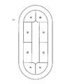
- FIG. 1 is a plan view illustrating a lateral diode according to an embodiment of the present disclosure
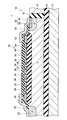
- 2 is a cross-sectional view of the lateral diode taken along line II-II in
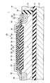
- 3 is a cross-sectional view of the lateral diode taken along line III-III in FIG.
- FIG. 4 is a diagram showing a corner portion and a straight portion of a horizontal diode
- FIG. 5 is a diagram showing a lateral diode according to a first modification.
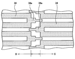
- FIG. 6 is a diagram showing the boundary between the straight portions C and D of the lateral diode according to the second modification.
- FIG. 1 is a plan view illustrating a lateral diode according to an embodiment of the present disclosure
- 2 is a cross-sectional view of the lateral diode taken along line II-II in
- 3 is a cross-sectional view of the lateral diode taken along line III-III in FIG.
- FIG. 4 is a diagram showing a corner portion
- FIG. 7 is a diagram showing the boundary between the straight portions C and D of the lateral diode according to the third modification.
- FIG. 8 is a diagram showing the concept of the resistance value of each part constituting the intermediate resistive field plate of the lateral diode according to the fourth modification
- FIG. 9 is a diagram showing the concept of the resistance value of the intermediate resistive field plate provided in each part of the lateral diode according to the fifth modification.
- the inventor of the present application has found the following points in the conventional lateral semiconductor device.
- the area between the cathode region and the anode region has a racetrack shape.
- the region between the cathode region and the anode region is not uniform along the circumferential direction, but includes a corner portion, a straight portion, and the like.
- an electric field tends to concentrate on a semiconductor layer corresponding to a corner portion. Therefore, in the semiconductor layer corresponding to the corner portion, it is desired that the length in the radial direction is longer than that of the straight portion.
- the spiral or concentric resistive field plate portion makes a round in the circumferential direction between the cathode region and the anode region, it is difficult to adopt different layouts for the corner portion and the straight portion. For this reason, when the corner portion and the straight portion are compared, the resistive field plate portion provided in the corner portion is disposed relatively less than the length between the cathode region and the anode region. Even if different layouts are adopted for the corner portion and the straight portion, a minute current flows through the contact portion as long as the resistive field plate portions of the corner portion and the straight portion are in contact with each other. , It will be affected to some extent. Considering these effects, a compromised layout that is not optimal for corners and straight lines must be adopted. The inventor of the present application has created the present invention by paying attention to the above points.
- the lateral semiconductor device is formed on a laminated substrate in which a support layer, a buried insulating layer, and an active layer are laminated.
- the laminated substrate is preferably an SOI substrate.
- the lateral semiconductor device is formed in an island region surrounded by an insulating isolation trench that goes around the active layer.
- a horizontal semiconductor device includes a semiconductor structure formed in a semiconductor layer.
- the semiconductor structure is composed of a plurality of types of semiconductor regions, and controls the current flowing through the semiconductor layer.
- a diode structure, an insulated gate bipolar transistor (IGBT) structure, a metal oxide semiconductor field effect transistor (MOSFET) structure, or the like is used as the semiconductor structure.
- the first semiconductor region is an n-type cathode region, and the second semiconductor region is a p-type anode region.
- the first semiconductor region is a p-type collector region, and the second semiconductor region is an n-type emitter region.
- the first semiconductor region is an n-type drain region, and the second semiconductor region is an n-type source region.
- a lateral diode 1 includes an SOI in which an n-type or p-type support layer 12, a buried insulating layer 14, and an n ⁇ -type active layer 16 are stacked. It is formed on the substrate 10. As shown in FIG. 1, the diode 1 is formed in an island region of the active layer 16 surrounded by the insulating isolation trench 18. The insulating isolation trench 18 extends from the surface of the active layer 16 to the buried insulating layer 14 through the active layer 16. The insulation isolation trench 18 circulates part of the active layer 16 when viewed in plan. In one example, single crystal silicon is used for the material of the support layer 12 and the active layer 16, and silicon oxide is used for the material of the buried insulating layer 14.
- the diode 1 includes an n-type cathode region 28, a p-type anode region 23, and an n-type drift region 26.
- the cathode region 28, the anode region 23, and the drift region 26 constitute a diode structure, and controls the current flowing in the lateral direction through the active layer 16. Specifically, when a forward bias is applied between the cathode region 28 and the anode region 23 (when the anode region 23 is connected to the high voltage side), a current is applied between the cathode region 28 and the anode region 23. Conduct.
- the cathode region 28 and the anode region 23 are made non-conductive.
- the cathode region 28 is disposed at the center of the island region and is formed to extend in one direction long.
- the cathode region 28 can be formed by implanting phosphorus ions into the surface portion of the active layer 16 using, for example, an ion implantation technique.
- the cathode region 28 is formed by one diffusion region, but instead of this example, the cathode region 28 may be formed in a state of being dispersed in one direction. Further, a p + type region may be partially formed so as to be in contact with the cathode region 28.
- the anode region 23 is arranged around the island region, and is formed around the cathode region 28 while being in contact with the insulating isolation trench 18.
- the anode region 23 has a high concentration anode region 22 and a low concentration anode region 24.
- the low concentration anode region 24 is formed deeper than the high concentration anode region 22 and surrounds the high concentration anode region 22.
- the forms of the high concentration anode region 22 and the low concentration anode region 24 are not limited to this example.
- the high concentration anode region 22 may be formed to have a smaller area and a part of the low concentration anode region 24 may be in contact with the anode electrode 32.
- the depth of the low concentration anode region 24 may be partially changed.
- the anode region 23 can be formed by implanting boron ions into the surface portion of the active layer 16 using, for example, an ion implantation technique.
- the drift region 26 is formed between the cathode region 28 and the anode region 23.
- the drift region 26 is a remaining part in which the cathode region 28 and the anode region 23 are formed in the active layer 16.
- a semiconductor region for example, a RESURF region for increasing the breakdown voltage may be formed as necessary.
- the diode 1 further includes a cathode electrode 36, an anode electrode 32, a local Oxidation of silicon (LOCOS) film 37 and a resistive field plate 30 provided on the surface of the active layer 16.
- LOCOS local Oxidation of silicon
- the cathode electrode 36 is disposed at the center of the island region and is in direct contact with the cathode region 28.
- the anode electrode 32 is disposed in the periphery of the island region and is in direct contact with the anode region 23.
- the LOCOS film 37 is provided on the surface of the active layer 16 and is disposed between the cathode region 28 and the anode region 23.
- the LOCOS film 37 is provided on the drift region 26.
- silicon oxide is used as the material of the LOCOS film 37.
- the resistive field plate 30 is provided on the surface of the LOCOS film 37, and has an inner peripheral resistive field plate portion 35, an intermediate resistive field plate portion 34, and an outer peripheral resistive field plate portion 33.
- the inner peripheral resistive field plate portion 35 is arranged so as to make a round around the central portion of the island-shaped region, and is electrically connected to the cathode region 28 via the cathode electrode 36.
- the outer peripheral resistive field plate portion 33 is arranged so as to go around the peripheral portion of the island-shaped region, and is connected to the anode region 23 via the anode electrode 32.
- the intermediate resistive field plate portion 34 is connected to both the inner peripheral resistive field plate portion 35 and the outer peripheral resistive field plate portion 33.
- the space between the cathode region 28 and the anode region 23 has a racetrack shape.
- the racetrack-like form includes corner portions A, B, E, and F and straight portions C, D, G, and H.
- each of the intermediate resistive field plate portions 34 formed in the portions A to H is in contact with the inner peripheral resistive field plate portion 35 at one end. The other end is in contact with the outer peripheral resistive field plate portion 33. Further, the intermediate resistive field plate portions 34 provided in the portions A to H are separated from the intermediate resistive field plate portions 34 provided in the adjacent portions.
- the intermediate resistive field plate portion 34 formed at the corner portions A, B, E, and F is formed by reciprocating between the cathode region 28 and the anode region 23 along the circumferential direction of the cathode region 28. .
- the intermediate resistive field plate portion 34 reciprocates 5 times between the cathode region 28 and the anode region 23.
- the length between the adjacent intermediate resistive field plate portions 34 is constant and fixed to a specific value.
- the intermediate resistive field plate portion 34 formed in the straight portions C, D, G, and H is formed by reciprocating between the cathode region 28 and the anode region 23 along the circumferential direction of the cathode region 28. .
- the intermediate resistive field plate portion 34 reciprocates four times between the cathode region 28 and the anode region 23.
- the length between the adjacent intermediate resistive field plate portions 34 is constant and fixed to a specific value.
- the length between the adjacent intermediate resistive field plate portions 34 and the straight portions C, D, G, and H when observed in the direction connecting the cathode region 28 and the anode region 23, the length between the adjacent intermediate resistive field plate portions 34 is the same.
- FIG. 2 shows an example of the intermediate resistive field plate portion 34 formed in the corner portions A, B, E, and F.
- FIG. 3 shows an example of the intermediate resistive field plate portion 34 formed in the straight portions C, D, G, and H.
- the electric field tends to concentrate.
- the length of the drift region 26 in the lateral direction that is, the length between the cathode region 28 and the anode region 23
- the length of the drift region 26 in the lateral direction is larger than the corner portions A, B, E, F than the straight portions C, D, G, H. Is longer.
- the intermediate resistive field plate portion 34 formed at the corner portions A, B, E, and F reciprocates more than the intermediate resistive field plate portion 34 formed at the straight portions C, D, G, and H. Many times are formed. Therefore, in any of the corner portions A, B, E, F and the straight portions C, D, G, H, the intermediate resistive field plate portion is uniformly above the drift region 26 over the entire portion. 34 is formed. That is, the arrangement interval of the intermediate resistive field plate portion 34 with respect to the lateral length of the drift region 26 is the same in the corner portions A, B, E, F and the straight portions C, D, G, H. Therefore, in any of the corner portions A, B, E, and F and the straight portions C, D, G, and H, the surface electric field of the drift region 26 is relaxed, and the high breakdown voltage diode 1 is realized.
- FIG. 5 shows a diode 1 according to a first modification of the present embodiment.
- a high-resistance semiconductor region 38 is formed between adjacent intermediate resistive field plate portions 34.
- the diode 1 is characterized in that the resistive field plate 30 and the semiconductor region 38 are formed using an ion implantation technique. Specifically, after a high resistance semiconductor layer is formed on the surface of the LOCOS film 37, a mask having an opening corresponding to a portion where the resistive field plate 30 is formed is patterned. Next, an impurity is introduced into the high resistance semiconductor layer through the opening, and the impurity is selectively introduced into a portion where the resistive field plate 30 is formed. After that, by performing an annealing process, the resistive field plate 30 and the semiconductor region 38 can be separately formed. When this manufacturing method is used, it is not necessary to use an etching technique, so that variations in processing can be suppressed.
- FIG. 6 is a diagram showing the boundary between the straight portions C and D of the horizontal diode 1 according to the second modification of the present embodiment.
- the intermediate resistive field plate portion 34 of the straight portion C has a protruding portion 34 a that protrudes toward the straight portion D.
- the intermediate resistive field plate portion 34 of the straight portion D also has a protruding portion 34 a that protrudes toward the straight portion C.
- the protruding portion 34a is repeatedly provided in the anode-cathode direction (vertical direction in FIG. 6).
- FIG. 7 is a diagram showing the boundary between the straight portions C and D of the horizontal diode 1 according to the third modification of the present embodiment.
- the protrusion 34a may be stepped as shown in FIG.
- the protruding portion 34a is provided as in the second and third modified examples, there is no blank portion where the intermediate resistive field plate portion 34 does not exist in the boundary portion between the straight portions C and D. For this reason, the surface electric field of the drift region 26 is relaxed also at the boundary portion between the straight portions C and D, and the high breakdown voltage diode 1 is realized. 6 and 7 exemplify the boundary portion between the straight portions C and D, it is naturally desirable that a similar structure is provided between the other portions.
- FIG. 8 is a diagram showing the concept of the resistance value of each part constituting the intermediate resistive field plate portion 34 of the horizontal diode 1 according to the fourth modification of the present embodiment.
- the intermediate resistive field plate portion 34 includes a plurality of portions (hereinafter referred to as arc portions) extending along the circumferential direction.
- the resistance value of the arc portion on the most cathode side (innermost circumference side) is R1
- the resistance value of the arc portion on the most anode side is RN.
- the circumferential length of the arc portion increases from the cathode side toward the anode side.
- the width of the intermediate resistive field plate portion 34 is constant, the relationship of R1 ⁇ R2 ⁇ R3 ⁇ .
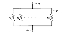
- FIG. 9 is a diagram showing a concept of the resistance value of the intermediate resistive field plate portion 34 provided in each part of the horizontal diode 1 according to the fifth modification of the present embodiment.
- the intermediate resistive field plate portions 34 formed in the portions A to H are connected in parallel between the inner peripheral resistive field plate portion 35 and the outer peripheral resistive field plate portion 33.
- the resistance value of the intermediate resistive field plate portion 34 formed at the corner portion A is Ra
- the resistance value of the intermediate resistive field plate portion 34 formed at the straight portion H is Rh.
- the current values flowing through the intermediate resistive field plate portions 34 are the same, current bias is suppressed, the surface electric field of the drift region 26 is relaxed, and the high breakdown voltage diode 1 is realized.
- the activation layer 16 is an example of a semiconductor layer
- the cathode region is an example of a first semiconductor region
- the anode region is an example of a second semiconductor region
- the LOCOS film 37 is an insulating layer. It is an example.
- the portions A to H two adjacent portions are examples of the first portion and the second portion, respectively, and the intermediate resistive field plate portion 34 provided in the first portion is the first resistive field plate portion.
- the intermediate resistive field plate portion 34 provided in the second portion is an example of the second resistive field plate portion.
- the semiconductor material using silicon is illustrated, but a wide gap semiconductor may be used instead of this example.
Landscapes
- Electrodes Of Semiconductors (AREA)
- Insulated Gate Type Field-Effect Transistor (AREA)
- Metal-Oxide And Bipolar Metal-Oxide Semiconductor Integrated Circuits (AREA)
Abstract
Description
Claims (6)
- 表面部に第1半導体領域(28)と、前記第1半導体領域の周囲を一巡している第2半導体領域(23)とを有する半導体層(16)と、
前記半導体層(16)の表面に設けられており、前記第1半導体領域(28)と前記第2半導体領域(23)の間に配置されている絶縁層(37)と、
前記絶縁層(37)の表面に設けられ、一端が前記第1半導体領域(28)に電気的に接続されており、他端が前記第2半導体領域(23)に電気的に接続されている抵抗性フィールドプレート(30)と、を備えた横型半導体装置であって、
平面視したときに、前記第1半導体領域(28)と前記第2半導体領域(23)の間には、前記第1半導体領域(28)の周囲を周方向に沿って隣り合う第1部分と第2部分が存在しており、
前記抵抗性フィールドプレート(30)は、前記第1部分に設けられており、前記周方向に沿って往復を繰返す第1抵抗性フィールドプレート部(34)と、前記第2部分に設けられており、前記周方向に沿って往復を繰返す第2抵抗性フィールドプレート部(34)と、を有しており、
前記第1部分に設けられている前記第1抵抗性フィールドプレート部(34)と前記第2部分に設けられている前記第2抵抗性フィールドプレート部(34)とが離れている横型半導体装置。 - 前記第1部分に設けられている前記第1抵抗性フィールドプレート部(34)の往復回数と前記第2部分に設けられている前記第2抵抗性フィールドプレート部(34)の往復回数が異なっている請求項1に記載の横型半導体装置。
- 平面視したときに、前記第1半導体領域(28)と前記第2半導体領域の間の領域(23)は、コーナー部分と直線部分を有しており、
前記第1部分は、前記コーナー部分に含まれており、
前記第2部分は、前記直線部分に含まれており、
前記第1部分に設けられている前記第1抵抗性フィールドプレート部(34)の往復回数は、前記第2部分に設けられている前記第2抵抗性フィールドプレート部(34)の往復回数よりも多い請求項2に記載の横型半導体装置。 - 前記第1抵抗性フィールドプレート部(34)は、前記周方向に沿って伸びる各部分の抵抗値が略等しい請求項3に記載の横型半導体装置。
- 前記第1抵抗性フィールドプレート部(34)は、第2部分に向けて突出する第1抵抗性フィールドプレート突出部(34a)を有しており、
前記第2抵抗性フィールドプレート部(34)は、第1部分に向けて突出する第2抵抗性フィールドプレート突出部(34a)を有しており、
平面視したときに、前記第1抵抗性フィールドプレート突出部(34a)と前記第2抵抗性フィールドプレート突出部(34a)が、前記第1半導体領域(28)と前記第2半導体領域(23)を結ぶ方向に沿って繰り返し設けられている請求項1~4のいずれか一項に記載の横型半導体装置。 - 前記第1抵抗性フィールドプレート部(34)の抵抗値と前記第2抵抗性フィールドプレート部(34)の抵抗値が略等しい請求項1~5のいずれか一項に記載の横型半導体装置。
Priority Applications (3)
| Application Number | Priority Date | Filing Date | Title |
|---|---|---|---|
| CN201280023653.0A CN103548147A (zh) | 2011-05-13 | 2012-05-10 | 横向半导体器件 |
| DE112012002075.8T DE112012002075T5 (de) | 2011-05-13 | 2012-05-10 | Laterale Halbleitervorrichtung |
| US14/113,419 US9240445B2 (en) | 2011-05-13 | 2012-05-10 | Lateral semiconductor device |
Applications Claiming Priority (4)
| Application Number | Priority Date | Filing Date | Title |
|---|---|---|---|
| JP2011-108485 | 2011-05-13 | ||
| JP2011108485 | 2011-05-13 | ||
| JP2012088455A JP5748353B2 (ja) | 2011-05-13 | 2012-04-09 | 横型半導体装置 |
| JP2012-088455 | 2012-04-09 |
Publications (1)
| Publication Number | Publication Date |
|---|---|
| WO2012157223A1 true WO2012157223A1 (ja) | 2012-11-22 |
Family
ID=47176575
Family Applications (1)
| Application Number | Title | Priority Date | Filing Date |
|---|---|---|---|
| PCT/JP2012/003065 Ceased WO2012157223A1 (ja) | 2011-05-13 | 2012-05-10 | 横型半導体装置 |
Country Status (5)
| Country | Link |
|---|---|
| US (1) | US9240445B2 (ja) |
| JP (1) | JP5748353B2 (ja) |
| CN (1) | CN103548147A (ja) |
| DE (1) | DE112012002075T5 (ja) |
| WO (1) | WO2012157223A1 (ja) |
Cited By (2)
| Publication number | Priority date | Publication date | Assignee | Title |
|---|---|---|---|---|
| US9048213B2 (en) | 2013-07-08 | 2015-06-02 | Renesas Electronics Corporation | Semiconductor device |
| US10115795B2 (en) | 2016-02-05 | 2018-10-30 | Renesas Electronics Corporation | Semiconductor device and method of manufacturing same |
Families Citing this family (9)
| Publication number | Priority date | Publication date | Assignee | Title |
|---|---|---|---|---|
| US10396167B2 (en) | 2015-12-15 | 2019-08-27 | Fuji Electric Co., Ltd. | Semiconductor device |
| JP6597269B2 (ja) | 2015-12-15 | 2019-10-30 | 富士電機株式会社 | 半導体装置 |
| JP6690336B2 (ja) | 2016-03-18 | 2020-04-28 | 富士電機株式会社 | 半導体装置 |
| JP6804379B2 (ja) * | 2017-04-24 | 2020-12-23 | 三菱電機株式会社 | 半導体装置 |
| JP6414861B2 (ja) * | 2017-09-12 | 2018-10-31 | ルネサスエレクトロニクス株式会社 | 半導体装置 |
| JP6910907B2 (ja) | 2017-09-25 | 2021-07-28 | ルネサスエレクトロニクス株式会社 | 半導体装置 |
| DE102017130213B4 (de) * | 2017-12-15 | 2021-10-21 | Infineon Technologies Ag | Planarer feldeffekttransistor |
| JP7140349B2 (ja) * | 2018-07-18 | 2022-09-21 | 株式会社東海理化電機製作所 | 半導体装置及びその製造方法 |
| CN118380461B (zh) * | 2024-01-09 | 2025-02-14 | 润新微电子(大连)有限公司 | 含可变电势多场板结构的器件 |
Citations (5)
| Publication number | Priority date | Publication date | Assignee | Title |
|---|---|---|---|---|
| JPH07326775A (ja) * | 1994-05-31 | 1995-12-12 | Sanken Electric Co Ltd | 半導体装置 |
| JP2000294803A (ja) * | 1998-11-05 | 2000-10-20 | Fuji Electric Co Ltd | 半導体装置 |
| JP2001352064A (ja) * | 2000-06-07 | 2001-12-21 | Fuji Electric Co Ltd | 高耐圧半導体装置 |
| JP2005005443A (ja) * | 2003-06-11 | 2005-01-06 | Toshiba Corp | 高耐圧半導体装置 |
| JP4362679B2 (ja) * | 2001-05-07 | 2009-11-11 | サンケン電気株式会社 | 半導体装置 |
Family Cites Families (9)
| Publication number | Priority date | Publication date | Assignee | Title |
|---|---|---|---|---|
| US5304836A (en) * | 1992-05-04 | 1994-04-19 | Xerox Corporation | High voltage field effect transistor having a small ratio of channel width to channel length and method of manufacture |
| JP3905981B2 (ja) | 1998-06-30 | 2007-04-18 | 株式会社東芝 | 高耐圧半導体装置 |
| US6603185B1 (en) | 1999-02-01 | 2003-08-05 | Fuji Electric Co., Ltd. | Voltage withstanding structure for a semiconductor device |
| US6525390B2 (en) * | 2000-05-18 | 2003-02-25 | Fuji Electric Co., Ltd. | MIS semiconductor device with low on resistance and high breakdown voltage |
| JP2002133625A (ja) * | 2000-10-24 | 2002-05-10 | Mitsumi Electric Co Ltd | ヘッド送り機構とそのバックラッシュ防止機構、およびアクチュエータアセンブリ |
| GB0107408D0 (en) * | 2001-03-23 | 2001-05-16 | Koninkl Philips Electronics Nv | Field effect transistor structure and method of manufacture |
| JP4757449B2 (ja) * | 2004-01-29 | 2011-08-24 | 三菱電機株式会社 | 半導体装置 |
| JP2007096006A (ja) * | 2005-09-29 | 2007-04-12 | Nippon Inter Electronics Corp | ガードリングの製造方法および半導体装置 |
| DE112010005272B4 (de) * | 2010-02-16 | 2014-12-24 | Sansha Electric Manufacturing Co., Ltd. | Pin-diode |
-
2012
- 2012-04-09 JP JP2012088455A patent/JP5748353B2/ja not_active Expired - Fee Related
- 2012-05-10 WO PCT/JP2012/003065 patent/WO2012157223A1/ja not_active Ceased
- 2012-05-10 CN CN201280023653.0A patent/CN103548147A/zh active Pending
- 2012-05-10 US US14/113,419 patent/US9240445B2/en not_active Expired - Fee Related
- 2012-05-10 DE DE112012002075.8T patent/DE112012002075T5/de not_active Withdrawn
Patent Citations (5)
| Publication number | Priority date | Publication date | Assignee | Title |
|---|---|---|---|---|
| JPH07326775A (ja) * | 1994-05-31 | 1995-12-12 | Sanken Electric Co Ltd | 半導体装置 |
| JP2000294803A (ja) * | 1998-11-05 | 2000-10-20 | Fuji Electric Co Ltd | 半導体装置 |
| JP2001352064A (ja) * | 2000-06-07 | 2001-12-21 | Fuji Electric Co Ltd | 高耐圧半導体装置 |
| JP4362679B2 (ja) * | 2001-05-07 | 2009-11-11 | サンケン電気株式会社 | 半導体装置 |
| JP2005005443A (ja) * | 2003-06-11 | 2005-01-06 | Toshiba Corp | 高耐圧半導体装置 |
Cited By (3)
| Publication number | Priority date | Publication date | Assignee | Title |
|---|---|---|---|---|
| US9048213B2 (en) | 2013-07-08 | 2015-06-02 | Renesas Electronics Corporation | Semiconductor device |
| US9343453B2 (en) | 2013-07-08 | 2016-05-17 | Renesas Electronics Corporation | Semiconductor device |
| US10115795B2 (en) | 2016-02-05 | 2018-10-30 | Renesas Electronics Corporation | Semiconductor device and method of manufacturing same |
Also Published As
| Publication number | Publication date |
|---|---|
| JP5748353B2 (ja) | 2015-07-15 |
| DE112012002075T5 (de) | 2014-03-06 |
| US20140048911A1 (en) | 2014-02-20 |
| CN103548147A (zh) | 2014-01-29 |
| JP2012256854A (ja) | 2012-12-27 |
| US9240445B2 (en) | 2016-01-19 |
Similar Documents
| Publication | Publication Date | Title |
|---|---|---|
| JP5748353B2 (ja) | 横型半導体装置 | |
| JP5900503B2 (ja) | 半導体装置 | |
| JP5196766B2 (ja) | 半導体装置 | |
| US8072029B2 (en) | High voltage semiconductor device with floating regions for reducing electric field concentration | |
| JP2017147431A (ja) | 半導体装置 | |
| JP7090073B2 (ja) | 半導体装置 | |
| JP2018120990A (ja) | 半導体装置 | |
| WO2012124786A1 (ja) | 半導体装置およびその製造方法 | |
| JP5537359B2 (ja) | 半導体装置 | |
| CN107112353A (zh) | 反向传导半导体装置 | |
| US10438946B2 (en) | Semiconductor device and electrical apparatus | |
| JP2019503591A (ja) | パワー半導体デバイス | |
| JP2016082167A (ja) | 半導体装置 | |
| JP5432751B2 (ja) | 半導体装置及び半導体装置の製造方法 | |
| JP2005093696A (ja) | 横型mosトランジスタ | |
| JP5904905B2 (ja) | 半導体装置 | |
| JP6299658B2 (ja) | 絶縁ゲート型スイッチング素子 | |
| JP2015070185A (ja) | 半導体装置及びその製造方法 | |
| JP2013201287A (ja) | パワー半導体装置 | |
| JP2015176900A (ja) | 半導体装置 | |
| JP2016189369A (ja) | 半導体装置 | |
| JP2006269633A (ja) | 電力用半導体装置 | |
| JP2021034528A (ja) | スイッチング素子 | |
| JP2016134480A (ja) | 半導体装置 | |
| JP6233012B2 (ja) | 半導体装置 |
Legal Events
| Date | Code | Title | Description |
|---|---|---|---|
| 121 | Ep: the epo has been informed by wipo that ep was designated in this application |
Ref document number: 12785817 Country of ref document: EP Kind code of ref document: A1 |
|
| WWE | Wipo information: entry into national phase |
Ref document number: 14113419 Country of ref document: US |
|
| WWE | Wipo information: entry into national phase |
Ref document number: 1120120020758 Country of ref document: DE Ref document number: 112012002075 Country of ref document: DE |
|
| 122 | Ep: pct application non-entry in european phase |
Ref document number: 12785817 Country of ref document: EP Kind code of ref document: A1 |