WO2012133314A1 - 導電性組成物、当該組成物を用いた導電性膜及びその製造方法 - Google Patents
導電性組成物、当該組成物を用いた導電性膜及びその製造方法 Download PDFInfo
- Publication number
- WO2012133314A1 WO2012133314A1 PCT/JP2012/057762 JP2012057762W WO2012133314A1 WO 2012133314 A1 WO2012133314 A1 WO 2012133314A1 JP 2012057762 W JP2012057762 W JP 2012057762W WO 2012133314 A1 WO2012133314 A1 WO 2012133314A1
- Authority
- WO
- WIPO (PCT)
- Prior art keywords
- conductive
- group
- film
- conductive composition
- composition
- Prior art date
Links
- XDWIEPSYNNSPSA-UHFFFAOYSA-N CCCCCCc(cc(C(C)C1CCCCC)c1c1)c1C#CC Chemical compound CCCCCCc(cc(C(C)C1CCCCC)c1c1)c1C#CC XDWIEPSYNNSPSA-UHFFFAOYSA-N 0.000 description 1
- BRONKZFUFDRSRA-UHFFFAOYSA-N C[N](C)(C)C(c1ccccc1)c1ccccc1 Chemical compound C[N](C)(C)C(c1ccccc1)c1ccccc1 BRONKZFUFDRSRA-UHFFFAOYSA-N 0.000 description 1
- KWMRYLJQSAHGCJ-UHFFFAOYSA-N C[N](C)(C)C1c2ccccc2-c2c1cccc2 Chemical compound C[N](C)(C)C1c2ccccc2-c2c1cccc2 KWMRYLJQSAHGCJ-UHFFFAOYSA-N 0.000 description 1
Images

Classifications
-
- B—PERFORMING OPERATIONS; TRANSPORTING
- B82—NANOTECHNOLOGY
- B82Y—SPECIFIC USES OR APPLICATIONS OF NANOSTRUCTURES; MEASUREMENT OR ANALYSIS OF NANOSTRUCTURES; MANUFACTURE OR TREATMENT OF NANOSTRUCTURES
- B82Y30/00—Nanotechnology for materials or surface science, e.g. nanocomposites
-
- C—CHEMISTRY; METALLURGY
- C08—ORGANIC MACROMOLECULAR COMPOUNDS; THEIR PREPARATION OR CHEMICAL WORKING-UP; COMPOSITIONS BASED THEREON
- C08K—Use of inorganic or non-macromolecular organic substances as compounding ingredients
- C08K3/00—Use of inorganic substances as compounding ingredients
- C08K3/02—Elements
- C08K3/04—Carbon
- C08K3/041—Carbon nanotubes
-
- C—CHEMISTRY; METALLURGY
- C08—ORGANIC MACROMOLECULAR COMPOUNDS; THEIR PREPARATION OR CHEMICAL WORKING-UP; COMPOSITIONS BASED THEREON
- C08K—Use of inorganic or non-macromolecular organic substances as compounding ingredients
- C08K5/00—Use of organic ingredients
- C08K5/0008—Organic ingredients according to more than one of the "one dot" groups of C08K5/01 - C08K5/59
-
- C—CHEMISTRY; METALLURGY
- C08—ORGANIC MACROMOLECULAR COMPOUNDS; THEIR PREPARATION OR CHEMICAL WORKING-UP; COMPOSITIONS BASED THEREON
- C08K—Use of inorganic or non-macromolecular organic substances as compounding ingredients
- C08K5/00—Use of organic ingredients
- C08K5/02—Halogenated hydrocarbons
- C08K5/03—Halogenated hydrocarbons aromatic, e.g. C6H5-CH2-Cl
-
- C—CHEMISTRY; METALLURGY
- C08—ORGANIC MACROMOLECULAR COMPOUNDS; THEIR PREPARATION OR CHEMICAL WORKING-UP; COMPOSITIONS BASED THEREON
- C08K—Use of inorganic or non-macromolecular organic substances as compounding ingredients
- C08K5/00—Use of organic ingredients
- C08K5/36—Sulfur-, selenium-, or tellurium-containing compounds
- C08K5/37—Thiols
- C08K5/372—Sulfides, e.g. R-(S)x-R'
-
- C—CHEMISTRY; METALLURGY
- C08—ORGANIC MACROMOLECULAR COMPOUNDS; THEIR PREPARATION OR CHEMICAL WORKING-UP; COMPOSITIONS BASED THEREON
- C08K—Use of inorganic or non-macromolecular organic substances as compounding ingredients
- C08K7/00—Use of ingredients characterised by shape
- C08K7/22—Expanded, porous or hollow particles
- C08K7/24—Expanded, porous or hollow particles inorganic
-
- C—CHEMISTRY; METALLURGY
- C09—DYES; PAINTS; POLISHES; NATURAL RESINS; ADHESIVES; COMPOSITIONS NOT OTHERWISE PROVIDED FOR; APPLICATIONS OF MATERIALS NOT OTHERWISE PROVIDED FOR
- C09D—COATING COMPOSITIONS, e.g. PAINTS, VARNISHES OR LACQUERS; FILLING PASTES; CHEMICAL PAINT OR INK REMOVERS; INKS; CORRECTING FLUIDS; WOODSTAINS; PASTES OR SOLIDS FOR COLOURING OR PRINTING; USE OF MATERIALS THEREFOR
- C09D165/00—Coating compositions based on macromolecular compounds obtained by reactions forming a carbon-to-carbon link in the main chain; Coating compositions based on derivatives of such polymers
-
- H—ELECTRICITY
- H01—ELECTRIC ELEMENTS
- H01B—CABLES; CONDUCTORS; INSULATORS; SELECTION OF MATERIALS FOR THEIR CONDUCTIVE, INSULATING OR DIELECTRIC PROPERTIES
- H01B1/00—Conductors or conductive bodies characterised by the conductive materials; Selection of materials as conductors
- H01B1/20—Conductive material dispersed in non-conductive organic material
- H01B1/24—Conductive material dispersed in non-conductive organic material the conductive material comprising carbon-silicon compounds, carbon or silicon
-
- H—ELECTRICITY
- H10—SEMICONDUCTOR DEVICES; ELECTRIC SOLID-STATE DEVICES NOT OTHERWISE PROVIDED FOR
- H10K—ORGANIC ELECTRIC SOLID-STATE DEVICES
- H10K30/00—Organic devices sensitive to infrared radiation, light, electromagnetic radiation of shorter wavelength or corpuscular radiation
- H10K30/80—Constructional details
- H10K30/81—Electrodes
- H10K30/82—Transparent electrodes, e.g. indium tin oxide [ITO] electrodes
- H10K30/821—Transparent electrodes, e.g. indium tin oxide [ITO] electrodes comprising carbon nanotubes
-
- H—ELECTRICITY
- H10—SEMICONDUCTOR DEVICES; ELECTRIC SOLID-STATE DEVICES NOT OTHERWISE PROVIDED FOR
- H10N—ELECTRIC SOLID-STATE DEVICES NOT OTHERWISE PROVIDED FOR
- H10N10/00—Thermoelectric devices comprising a junction of dissimilar materials, i.e. devices exhibiting Seebeck or Peltier effects
- H10N10/80—Constructional details
- H10N10/85—Thermoelectric active materials
-
- C—CHEMISTRY; METALLURGY
- C08—ORGANIC MACROMOLECULAR COMPOUNDS; THEIR PREPARATION OR CHEMICAL WORKING-UP; COMPOSITIONS BASED THEREON
- C08G—MACROMOLECULAR COMPOUNDS OBTAINED OTHERWISE THAN BY REACTIONS ONLY INVOLVING UNSATURATED CARBON-TO-CARBON BONDS
- C08G2261/00—Macromolecular compounds obtained by reactions forming a carbon-to-carbon link in the main chain of the macromolecule
- C08G2261/10—Definition of the polymer structure
- C08G2261/12—Copolymers
- C08G2261/124—Copolymers alternating
-
- C—CHEMISTRY; METALLURGY
- C08—ORGANIC MACROMOLECULAR COMPOUNDS; THEIR PREPARATION OR CHEMICAL WORKING-UP; COMPOSITIONS BASED THEREON
- C08G—MACROMOLECULAR COMPOUNDS OBTAINED OTHERWISE THAN BY REACTIONS ONLY INVOLVING UNSATURATED CARBON-TO-CARBON BONDS
- C08G2261/00—Macromolecular compounds obtained by reactions forming a carbon-to-carbon link in the main chain of the macromolecule
- C08G2261/10—Definition of the polymer structure
- C08G2261/13—Morphological aspects
- C08G2261/135—Cross-linked structures
-
- C—CHEMISTRY; METALLURGY
- C08—ORGANIC MACROMOLECULAR COMPOUNDS; THEIR PREPARATION OR CHEMICAL WORKING-UP; COMPOSITIONS BASED THEREON
- C08G—MACROMOLECULAR COMPOUNDS OBTAINED OTHERWISE THAN BY REACTIONS ONLY INVOLVING UNSATURATED CARBON-TO-CARBON BONDS
- C08G2261/00—Macromolecular compounds obtained by reactions forming a carbon-to-carbon link in the main chain of the macromolecule
- C08G2261/10—Definition of the polymer structure
- C08G2261/14—Side-groups
- C08G2261/141—Side-chains having aliphatic units
- C08G2261/1412—Saturated aliphatic units
-
- C—CHEMISTRY; METALLURGY
- C08—ORGANIC MACROMOLECULAR COMPOUNDS; THEIR PREPARATION OR CHEMICAL WORKING-UP; COMPOSITIONS BASED THEREON
- C08G—MACROMOLECULAR COMPOUNDS OBTAINED OTHERWISE THAN BY REACTIONS ONLY INVOLVING UNSATURATED CARBON-TO-CARBON BONDS
- C08G2261/00—Macromolecular compounds obtained by reactions forming a carbon-to-carbon link in the main chain of the macromolecule
- C08G2261/10—Definition of the polymer structure
- C08G2261/14—Side-groups
- C08G2261/142—Side-chains containing oxygen
- C08G2261/1424—Side-chains containing oxygen containing ether groups, including alkoxy
-
- C—CHEMISTRY; METALLURGY
- C08—ORGANIC MACROMOLECULAR COMPOUNDS; THEIR PREPARATION OR CHEMICAL WORKING-UP; COMPOSITIONS BASED THEREON
- C08G—MACROMOLECULAR COMPOUNDS OBTAINED OTHERWISE THAN BY REACTIONS ONLY INVOLVING UNSATURATED CARBON-TO-CARBON BONDS
- C08G2261/00—Macromolecular compounds obtained by reactions forming a carbon-to-carbon link in the main chain of the macromolecule
- C08G2261/30—Monomer units or repeat units incorporating structural elements in the main chain
- C08G2261/32—Monomer units or repeat units incorporating structural elements in the main chain incorporating heteroaromatic structural elements in the main chain
- C08G2261/322—Monomer units or repeat units incorporating structural elements in the main chain incorporating heteroaromatic structural elements in the main chain non-condensed
- C08G2261/3223—Monomer units or repeat units incorporating structural elements in the main chain incorporating heteroaromatic structural elements in the main chain non-condensed containing one or more sulfur atoms as the only heteroatom, e.g. thiophene
-
- C—CHEMISTRY; METALLURGY
- C08—ORGANIC MACROMOLECULAR COMPOUNDS; THEIR PREPARATION OR CHEMICAL WORKING-UP; COMPOSITIONS BASED THEREON
- C08G—MACROMOLECULAR COMPOUNDS OBTAINED OTHERWISE THAN BY REACTIONS ONLY INVOLVING UNSATURATED CARBON-TO-CARBON BONDS
- C08G2261/00—Macromolecular compounds obtained by reactions forming a carbon-to-carbon link in the main chain of the macromolecule
- C08G2261/30—Monomer units or repeat units incorporating structural elements in the main chain
- C08G2261/32—Monomer units or repeat units incorporating structural elements in the main chain incorporating heteroaromatic structural elements in the main chain
- C08G2261/324—Monomer units or repeat units incorporating structural elements in the main chain incorporating heteroaromatic structural elements in the main chain condensed
- C08G2261/3243—Monomer units or repeat units incorporating structural elements in the main chain incorporating heteroaromatic structural elements in the main chain condensed containing one or more sulfur atoms as the only heteroatom, e.g. benzothiophene
-
- C—CHEMISTRY; METALLURGY
- C08—ORGANIC MACROMOLECULAR COMPOUNDS; THEIR PREPARATION OR CHEMICAL WORKING-UP; COMPOSITIONS BASED THEREON
- C08G—MACROMOLECULAR COMPOUNDS OBTAINED OTHERWISE THAN BY REACTIONS ONLY INVOLVING UNSATURATED CARBON-TO-CARBON BONDS
- C08G2261/00—Macromolecular compounds obtained by reactions forming a carbon-to-carbon link in the main chain of the macromolecule
- C08G2261/30—Monomer units or repeat units incorporating structural elements in the main chain
- C08G2261/34—Monomer units or repeat units incorporating structural elements in the main chain incorporating partially-aromatic structural elements in the main chain
- C08G2261/342—Monomer units or repeat units incorporating structural elements in the main chain incorporating partially-aromatic structural elements in the main chain containing only carbon atoms
- C08G2261/3422—Monomer units or repeat units incorporating structural elements in the main chain incorporating partially-aromatic structural elements in the main chain containing only carbon atoms conjugated, e.g. PPV-type
-
- C—CHEMISTRY; METALLURGY
- C08—ORGANIC MACROMOLECULAR COMPOUNDS; THEIR PREPARATION OR CHEMICAL WORKING-UP; COMPOSITIONS BASED THEREON
- C08G—MACROMOLECULAR COMPOUNDS OBTAINED OTHERWISE THAN BY REACTIONS ONLY INVOLVING UNSATURATED CARBON-TO-CARBON BONDS
- C08G2261/00—Macromolecular compounds obtained by reactions forming a carbon-to-carbon link in the main chain of the macromolecule
- C08G2261/50—Physical properties
- C08G2261/51—Charge transport
-
- C—CHEMISTRY; METALLURGY
- C08—ORGANIC MACROMOLECULAR COMPOUNDS; THEIR PREPARATION OR CHEMICAL WORKING-UP; COMPOSITIONS BASED THEREON
- C08G—MACROMOLECULAR COMPOUNDS OBTAINED OTHERWISE THAN BY REACTIONS ONLY INVOLVING UNSATURATED CARBON-TO-CARBON BONDS
- C08G2261/00—Macromolecular compounds obtained by reactions forming a carbon-to-carbon link in the main chain of the macromolecule
- C08G2261/50—Physical properties
- C08G2261/55—Physical properties thermoelectric
-
- C—CHEMISTRY; METALLURGY
- C08—ORGANIC MACROMOLECULAR COMPOUNDS; THEIR PREPARATION OR CHEMICAL WORKING-UP; COMPOSITIONS BASED THEREON
- C08G—MACROMOLECULAR COMPOUNDS OBTAINED OTHERWISE THAN BY REACTIONS ONLY INVOLVING UNSATURATED CARBON-TO-CARBON BONDS
- C08G2261/00—Macromolecular compounds obtained by reactions forming a carbon-to-carbon link in the main chain of the macromolecule
- C08G2261/70—Post-treatment
- C08G2261/76—Post-treatment crosslinking
-
- C—CHEMISTRY; METALLURGY
- C08—ORGANIC MACROMOLECULAR COMPOUNDS; THEIR PREPARATION OR CHEMICAL WORKING-UP; COMPOSITIONS BASED THEREON
- C08G—MACROMOLECULAR COMPOUNDS OBTAINED OTHERWISE THAN BY REACTIONS ONLY INVOLVING UNSATURATED CARBON-TO-CARBON BONDS
- C08G2261/00—Macromolecular compounds obtained by reactions forming a carbon-to-carbon link in the main chain of the macromolecule
- C08G2261/70—Post-treatment
- C08G2261/79—Post-treatment doping
- C08G2261/792—Post-treatment doping with low-molecular weight dopants
-
- C—CHEMISTRY; METALLURGY
- C08—ORGANIC MACROMOLECULAR COMPOUNDS; THEIR PREPARATION OR CHEMICAL WORKING-UP; COMPOSITIONS BASED THEREON
- C08G—MACROMOLECULAR COMPOUNDS OBTAINED OTHERWISE THAN BY REACTIONS ONLY INVOLVING UNSATURATED CARBON-TO-CARBON BONDS
- C08G2261/00—Macromolecular compounds obtained by reactions forming a carbon-to-carbon link in the main chain of the macromolecule
- C08G2261/90—Applications
-
- C—CHEMISTRY; METALLURGY
- C08—ORGANIC MACROMOLECULAR COMPOUNDS; THEIR PREPARATION OR CHEMICAL WORKING-UP; COMPOSITIONS BASED THEREON
- C08G—MACROMOLECULAR COMPOUNDS OBTAINED OTHERWISE THAN BY REACTIONS ONLY INVOLVING UNSATURATED CARBON-TO-CARBON BONDS
- C08G61/00—Macromolecular compounds obtained by reactions forming a carbon-to-carbon link in the main chain of the macromolecule
- C08G61/02—Macromolecular compounds containing only carbon atoms in the main chain of the macromolecule, e.g. polyxylylenes
- C08G61/04—Macromolecular compounds containing only carbon atoms in the main chain of the macromolecule, e.g. polyxylylenes only aliphatic carbon atoms
-
- C—CHEMISTRY; METALLURGY
- C08—ORGANIC MACROMOLECULAR COMPOUNDS; THEIR PREPARATION OR CHEMICAL WORKING-UP; COMPOSITIONS BASED THEREON
- C08G—MACROMOLECULAR COMPOUNDS OBTAINED OTHERWISE THAN BY REACTIONS ONLY INVOLVING UNSATURATED CARBON-TO-CARBON BONDS
- C08G61/00—Macromolecular compounds obtained by reactions forming a carbon-to-carbon link in the main chain of the macromolecule
- C08G61/12—Macromolecular compounds containing atoms other than carbon in the main chain of the macromolecule
- C08G61/122—Macromolecular compounds containing atoms other than carbon in the main chain of the macromolecule derived from five- or six-membered heterocyclic compounds, other than imides
- C08G61/123—Macromolecular compounds containing atoms other than carbon in the main chain of the macromolecule derived from five- or six-membered heterocyclic compounds, other than imides derived from five-membered heterocyclic compounds
- C08G61/126—Macromolecular compounds containing atoms other than carbon in the main chain of the macromolecule derived from five- or six-membered heterocyclic compounds, other than imides derived from five-membered heterocyclic compounds with a five-membered ring containing one sulfur atom in the ring
-
- C—CHEMISTRY; METALLURGY
- C08—ORGANIC MACROMOLECULAR COMPOUNDS; THEIR PREPARATION OR CHEMICAL WORKING-UP; COMPOSITIONS BASED THEREON
- C08K—Use of inorganic or non-macromolecular organic substances as compounding ingredients
- C08K2201/00—Specific properties of additives
- C08K2201/011—Nanostructured additives
-
- C—CHEMISTRY; METALLURGY
- C08—ORGANIC MACROMOLECULAR COMPOUNDS; THEIR PREPARATION OR CHEMICAL WORKING-UP; COMPOSITIONS BASED THEREON
- C08K—Use of inorganic or non-macromolecular organic substances as compounding ingredients
- C08K5/00—Use of organic ingredients
- C08K5/36—Sulfur-, selenium-, or tellurium-containing compounds
- C08K5/43—Compounds containing sulfur bound to nitrogen
-
- C—CHEMISTRY; METALLURGY
- C08—ORGANIC MACROMOLECULAR COMPOUNDS; THEIR PREPARATION OR CHEMICAL WORKING-UP; COMPOSITIONS BASED THEREON
- C08K—Use of inorganic or non-macromolecular organic substances as compounding ingredients
- C08K5/00—Use of organic ingredients
- C08K5/55—Boron-containing compounds
-
- Y—GENERAL TAGGING OF NEW TECHNOLOGICAL DEVELOPMENTS; GENERAL TAGGING OF CROSS-SECTIONAL TECHNOLOGIES SPANNING OVER SEVERAL SECTIONS OF THE IPC; TECHNICAL SUBJECTS COVERED BY FORMER USPC CROSS-REFERENCE ART COLLECTIONS [XRACs] AND DIGESTS
- Y02—TECHNOLOGIES OR APPLICATIONS FOR MITIGATION OR ADAPTATION AGAINST CLIMATE CHANGE
- Y02E—REDUCTION OF GREENHOUSE GAS [GHG] EMISSIONS, RELATED TO ENERGY GENERATION, TRANSMISSION OR DISTRIBUTION
- Y02E10/00—Energy generation through renewable energy sources
- Y02E10/50—Photovoltaic [PV] energy
- Y02E10/549—Organic PV cells
-
- Y—GENERAL TAGGING OF NEW TECHNOLOGICAL DEVELOPMENTS; GENERAL TAGGING OF CROSS-SECTIONAL TECHNOLOGIES SPANNING OVER SEVERAL SECTIONS OF THE IPC; TECHNICAL SUBJECTS COVERED BY FORMER USPC CROSS-REFERENCE ART COLLECTIONS [XRACs] AND DIGESTS
- Y02—TECHNOLOGIES OR APPLICATIONS FOR MITIGATION OR ADAPTATION AGAINST CLIMATE CHANGE
- Y02P—CLIMATE CHANGE MITIGATION TECHNOLOGIES IN THE PRODUCTION OR PROCESSING OF GOODS
- Y02P20/00—Technologies relating to chemical industry
- Y02P20/10—Process efficiency
- Y02P20/129—Energy recovery, e.g. by cogeneration, H2recovery or pressure recovery turbines
-
- Y—GENERAL TAGGING OF NEW TECHNOLOGICAL DEVELOPMENTS; GENERAL TAGGING OF CROSS-SECTIONAL TECHNOLOGIES SPANNING OVER SEVERAL SECTIONS OF THE IPC; TECHNICAL SUBJECTS COVERED BY FORMER USPC CROSS-REFERENCE ART COLLECTIONS [XRACs] AND DIGESTS
- Y02—TECHNOLOGIES OR APPLICATIONS FOR MITIGATION OR ADAPTATION AGAINST CLIMATE CHANGE
- Y02P—CLIMATE CHANGE MITIGATION TECHNOLOGIES IN THE PRODUCTION OR PROCESSING OF GOODS
- Y02P70/00—Climate change mitigation technologies in the production process for final industrial or consumer products
- Y02P70/50—Manufacturing or production processes characterised by the final manufactured product
Definitions
- the present invention relates to a conductive composition using carbon nanotubes, a conductive film using the composition, and a method for producing the same.
- image display elements represented by liquid crystal displays (LCDs), plasma displays (PDPs), electroluminescence (EL) elements, etc.
- LCDs liquid crystal displays
- PDPs plasma displays
- EL electroluminescence
- a transparent conductive film is used for such display elements and solar cells.
- a metal material such as ITO (indium tin oxide) is generally used for the transparent conductive film, and the metal material is formed on a glass substrate by a vapor phase method such as a vacuum evaporation method or a sputtering method. Formed.
- a vapor phase method such as a vacuum evaporation method or a sputtering method.
- the production apparatus and the like are expensive, and it is difficult to increase the film production area.
- electrical devices such as mobile phones and mobile devices, there is a great demand for weight reduction and flexibility. For this reason, it has been studied to shift the substrate material from glass to plastic.
- the weight of the display device can be reduced to half or less that of a glass substrate, and the strength and impact resistance can be significantly improved.
- the conventional vapor phase manufacturing requires heat resistance of the substrate, so that the plastic substrate lacks heat resistance.
- substrate of the formed film fell and produced problems, such as being easy to peel off.
- conductive materials containing nanocarbon materials such as carbon nanotubes
- film formation by spin coating and other coating methods is possible, so high temperature and vacuum conditions are not essential.
- the manufacturing process is simple and the manufacturing cost can be reduced. Since materials such as plastic can also be used as a substrate, it is possible to cope with weight reduction and flexibility of the device, and in addition, the strength and impact resistance can be remarkably improved. It is also suitable for manufacturing large area films and the like. From such advantages, the development and practical application of new conductive materials using nanocarbon materials are expected.
- CNT carbon nanotubes
- liquid dispersibility is a problem to be solved.
- CNT carbon nanotubes
- CNT easily aggregates and is not easily dispersed. Therefore, the dispersion of CNTs is improved by adding a dispersant, and the obtained dispersion is applied and formed into a film (see, for example, Non-Patent Documents 1 and 2).
- Non-Patent Document 3 a method has been proposed in which a conjugated polymer capable of transferring charge to and from CNTs, a so-called conductive polymer, is used to disperse CNTs in a solution of the polymer and to increase dispersibility.
- a conjugated polymer capable of transferring charge to and from CNTs a so-called conductive polymer
- Patent Documents 4 to 9 and Non-Patent Document 4 it is difficult to sufficiently exhibit the original high conductivity of CNT.
- An object of the present invention is to provide a conductive composition having good dispersibility of CNTs, high conductivity, and excellent coating properties, a conductive film using the composition, and a method for producing the same. And Moreover, this invention makes it a subject to provide the thermoelectric conversion element using the thermoelectric conversion material excellent in the thermoelectric conversion performance which uses the said composition, and the said electroconductive film and electroconductive laminated body.
- the present inventors have intensively studied in view of the above problems. As a result, in the conventional method of increasing the dispersibility of CNTs using a conductive polymer, the conductivity and the semiconductor properties are deteriorated in the process of charge transfer in the conductive polymer. It was found that can not be demonstrated. And it discovered that the new electroconductive composition with which the high electroconductivity which CNT originally has was exhibited was obtained by containing an onium salt compound with CNT and a conductive polymer. Furthermore, the composition has excellent thermoelectric conversion performance, and was suitably used as a thermoelectric conversion material. The present invention has been made based on this finding.
- the (C) onium salt compound is a compound having an oxidizing ability with respect to (A) a carbon nanotube and / or (B) a conductive polymer. Sex composition.
- the (C) onium salt compound is a compound that generates an acid upon application of heat or active energy ray irradiation.
- R 21 to R 23 , R 25 to R 26 and R 31 to R 33 are each independently a linear, branched or cyclic alkyl group, aralkyl group, aryl group, R 27 to R 30 each independently represents a hydrogen atom, a linear, branched or cyclic alkyl group, an aralkyl group, an aryl group, an aromatic heterocyclic group, an alkoxy group, an aryloxy group R 24 represents a linear, branched or cyclic alkylene group or an arylene group, and R 21 to R 33 may be further substituted.
- X ⁇ represents an anion of a strong acid.
- Any two groups of R 21 ⁇ R 23 in the general formula (I) is, R 21 and R 23 in the general formula (II) is, the R 25 and R 26 in formula (III), general formula (IV)
- Any two groups of R 27 to R 30 are bonded to any two groups of R 31 to R 33 in the general formula (V) to form an aliphatic ring, an aromatic ring, or a heterocyclic ring, respectively. May be.
- X ⁇ represents an anion of an aryl sulfonic acid, an anion of a perfluoroalkyl sulfonic acid, an anion of a perhalogenated Lewis acid, an anion of a perfluoroalkyl sulfonimide,
- ⁇ 6> The conductive composition according to any one of ⁇ 1> to ⁇ 5>, wherein the (A) carbon nanotubes are uniformly dispersed in the composition.
- ⁇ 7> The conductive composition according to any one of ⁇ 1> to ⁇ 6>, further including a solvent.
- ⁇ 8> In the total solid content of the conductive composition, (A) 3 to 50% by mass of carbon nanotubes, (B) 30 to 80% by mass of conductive polymer, and (C) 1 to 50 of onium salt compound.
- ⁇ 9> The conductive composition according to any one of ⁇ 1> to ⁇ 8>, which is for thermoelectric conversion.
- ⁇ 11> A conductive film obtained by molding the conductive composition according to any one of ⁇ 1> to ⁇ 9>, and applying heat or active energy rays after molding.
- ⁇ 12> A conductive laminate including a base material and the conductive film according to the above ⁇ 10> or ⁇ 11> provided on the base material.
- ⁇ 13> A conductive laminate obtained by applying the conductive composition according to any one of ⁇ 1> to ⁇ 9> on a substrate.
- ⁇ 14> A conductive laminate obtained by applying the conductive composition according to any one of ⁇ 1> to ⁇ 9> on a substrate, and applying heat or active energy rays after the application.
- ⁇ 15> The conductive laminate according to any one of ⁇ 12> to ⁇ 14>, wherein the base material is a resin film.
- ⁇ 16> The conductive laminate according to any one of ⁇ 12> to ⁇ 15>, further comprising an electrode.
- ⁇ 17> A thermoelectric conversion element comprising the conductive film according to ⁇ 10> or ⁇ 11>, or the conductive laminate according to any one of ⁇ 12> to ⁇ 16>.
- ⁇ 18> The conductive composition according to any one of ⁇ 1> to ⁇ 9>, the conductive film according to ⁇ 10> or ⁇ 11>, and any of ⁇ 12> to ⁇ 16> A conductive article using any one of the conductive laminates according to claim 1.
- thermoelectric generator using the thermoelectric conversion element according to ⁇ 17> A thermoelectric generator using the thermoelectric conversion element according to ⁇ 17>.
- a method for producing a conductive film comprising a step of molding the conductive composition according to any one of ⁇ 1> to ⁇ 9>.
- the conductive composition of the present invention has a high conductivity without CNTs being uniformly dispersed and the excellent electrical conductivity of the CNTs being impaired, and the conductive composition liquid has excellent coating properties on the substrate. Therefore, it can be suitably used for the production of a conductive film (film), a conductive layer and the like.
- the conductive film of the present invention produced using the composition has high conductivity and good film quality, and can be used for a wide range of applications as a conductive material.
- the conductive composition and the conductive film of the present invention are used for transparent electrodes, capacitors, capacitors, secondary batteries and the like used in various display elements typified by liquid crystal displays and solar cells. It is useful as an organic semiconductor material such as a conductive material, a photoelectric conversion element, a thermoelectric conversion element, and an organic FET.
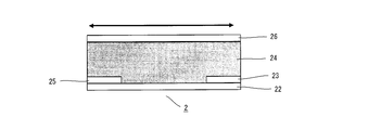
- thermoelectric conversion element of this invention It is a figure which shows typically an example of the thermoelectric conversion element of this invention.
- the arrows in FIG. 1 indicate the direction of the temperature difference applied when the element is used.
- FIG. 2 It is a figure which shows typically an example of the thermoelectric conversion element of this invention.
- the arrows in FIG. 2 indicate the direction of the temperature difference applied when the element is used.
- the conductive composition of the present invention contains (B) a conductive polymer and (C) an onium salt compound together with (A) CNT.
- a conductive polymer By using a conductive polymer, the dispersibility of CNTs in the composition can be increased, and excellent coating properties can be realized without impairing conductivity. Furthermore, by using an onium salt compound, the conductivity of the composition can be dramatically increased. With these compositions, the composition can be easily formed by coating, and the formed coating film has high conductivity and good film quality. Further, the composition has excellent thermoelectric conversion performance in addition to this high conductivity, and can be suitably used as a thermoelectric conversion material.
- the conductive composition of the present invention will be described in detail.
- a CNT is a single-walled CNT in which a single carbon film (graphene sheet) is wound in a cylindrical shape, a double-walled CNT in which two graphene sheets are wound in a concentric shape, and a plurality of graphene sheets in a concentric circle There are multi-walled CNTs wound in a shape.
- single-walled CNTs, double-walled CNTs, and multilayered CNTs may be used alone, or two or more kinds may be used in combination.
- Single-walled CNTs may be semiconducting or metallic, and both may be used in combination.
- the content ratio of both in the composition can be appropriately adjusted according to the use of the composition.
- the content ratio of metallic CNT is high from the viewpoint of conductivity.
- the content ratio of semiconducting CNTs is high from the viewpoint of semiconductor characteristics.
- the CNT may contain a metal or the like, or may contain a molecule such as fullerene.
- the conductive composition of the present invention may contain nanocarbons such as carbon nanohorns, carbon nanocoils, and carbon nanobeads in addition to CNTs.
- CNT can be produced by an arc discharge method, a chemical vapor deposition method (hereinafter referred to as a CVD method), a laser ablation method, or the like.
- the CNT used in the present invention may be obtained by any method, but is preferably obtained by an arc discharge method and a CVD method.
- a CVD method chemical vapor deposition method
- fullerene, graphite, and amorphous carbon are simultaneously generated as by-products, and catalyst metals such as nickel, iron, cobalt, and yttrium remain.
- purification is preferably performed.
- the method for purifying CNTs is not particularly limited, but acid treatment with nitric acid, sulfuric acid, etc., and ultrasonic treatment are effective for removing impurities.
- CNT can be used as it is.
- CNT since CNT is generally produced in a string shape, it may be cut into a desired length depending on the application. For example, when used for semiconductor applications, it is preferable to use CNT shorter than the distance between element electrodes in order to prevent short circuit between element electrodes.
- CNTs can be cut into short fibers by acid treatment with nitric acid, sulfuric acid or the like, ultrasonic treatment, freeze pulverization method or the like. In addition, it is also preferable to perform separation using a filter from the viewpoint of improving purity. In the present invention, not only cut CNTs but also CNTs produced in the form of short fibers in advance can be used in the same manner.
- Such short fibrous CNTs are formed by forming a catalytic metal such as iron or cobalt on a substrate and thermally decomposing a carbon compound at 700 to 900 ° C. on the surface by CVD to vapor-phase grow CNTs. Thus, a shape oriented in the direction perpendicular to the substrate surface is obtained.
- the short fiber CNTs thus produced can be taken out by a method such as peeling off from the substrate.
- the short fibrous CNTs can be obtained by supporting a catalytic metal on a porous support such as porous silicon or an anodic oxide film of alumina and growing the CNTs on the surface by the CVD method.
- oriented molecules such as iron phthalocyanine containing a catalytic metal in the molecule as a raw material and producing CNTs on a substrate by performing CVD in an argon / hydrogen gas flow, producing oriented short fiber CNTs You can also. Furthermore, it is also possible to obtain short fiber CNTs oriented on the SiC single crystal surface by an epitaxial growth method.
- the average length of the CNTs used in the present invention is not particularly limited, and can be appropriately selected according to the use of the composition.
- the average length of CNTs is 0.01 ⁇ m or more and 1000 ⁇ m from the viewpoints of manufacturability, film formability, conductivity, etc., depending on the distance between electrodes. Or less, more preferably 0.1 ⁇ m or more and 100 ⁇ m or less.
- the diameter of the CNT used in the present invention is not particularly limited, but is preferably 0.4 nm or more and 100 nm or less, more preferably 50 nm or less, and still more preferably, from the viewpoint of durability, transparency, film formability, conductivity, and the like. Is 15 nm or less.
- the conductive polymer used in the present invention is a polymer compound having a conjugated molecular structure.
- the polymer having a conjugated molecular structure refers to a polymer having a structure in which single bonds and double bonds are alternately connected in a carbon-carbon bond on the main chain of the polymer.
- the conductive polymer used in the present invention is not necessarily a high molecular weight compound, and may be an oligomer compound.
- conductive polymer used in the present invention examples include thiophene compounds, pyrrole compounds, aniline compounds, acetylene compounds, p-phenylene compounds, p-phenylene vinylene compounds, p-phenylene ethynylene.
- the substituent introduced into the above derivative is not particularly limited, but in consideration of compatibility with other components, the type of medium that can be used, etc., CNT, conductive polymer, onium salt in the composition It is preferable to appropriately select and introduce a group capable of enhancing the dispersibility and solubility of the compound.
- a group capable of enhancing the dispersibility and solubility of the compound when an organic solvent is used as a medium, an alkoxyalkyleneoxy group, an alkoxyalkyleneoxyalkyl group, a crown ether group, an aryl group, or the like is preferably used in addition to a linear, branched, or cyclic alkyl group, alkoxy group, or thioalkyl group. be able to.
- These groups may further have a substituent.
- the carbon number of the substituent is not particularly limited, but is preferably 1 to 12, more preferably 4 to 12, and particularly a long-chain alkyl group, alkoxy group, thioalkyl group having 6 to 12 carbon atoms.
- An alkoxyalkyleneoxy group and an alkoxyalkyleneoxyalkyl group are preferred.
- a hydrophilic group such as a carboxylic acid group, a sulfonic acid group, a hydroxyl group, or a phosphoric acid group to the terminal of each monomer or the above substituent.
- An alkoxy group or the like can be introduced as a substituent, which is preferable.
- the number of substituents that can be introduced is not particularly limited, and one or more substituents can be appropriately introduced in consideration of dispersibility, compatibility, conductivity, and the like of CNTs and conductive polymers. .
- Examples of the conjugated polymer having a repeating unit derived from a thiophene compound and a derivative thereof include polythiophene, a conjugated polymer containing a repeating unit derived from a monomer having a substituent introduced into the thiophene ring, and a thiophene ring. And a conjugated polymer containing a repeating unit derived from a monomer having a condensed polycyclic structure.
- Examples of the conjugated polymer containing a repeating unit derived from a monomer having a substituent introduced into the thiophene ring include poly-3-methylthiophene, poly-3-butylthiophene, poly-3-hexylthiophene, poly-3- Cyclohexylthiophene, poly-3- (2′-ethylhexyl) thiophene, poly-3-octylthiophene, poly-3-dodecylthiophene, poly-3- (2′-methoxyethoxy) methylthiophene, poly-3- (methoxyethoxy) Poly-alkyl-substituted thiophenes such as ethoxy) methylthiophene, poly-3-methoxythiophene, poly-3-ethoxythiophene, poly-3-hexyloxythiophene, poly-3-cyclohexyloxythiophene, poly-3- (2 ′ -Ethy
- poly-3-alkylthiophenes and poly-3-alkoxythiophenes are preferable.
- anisotropy occurs depending on the direction of bonding at the 2,5-position of the thiophene ring.
- a conjugated polymer including a repeating unit derived from a monomer having a substituent introduced into a thiophene ring and a conjugated polymer including a repeating unit derived from a monomer having a condensed polycyclic structure including a thiophene ring.
- the following compounds can be exemplified as: In the following formula, n represents an integer of 10 or more.
- Examples of the conjugated polymer having a repeating unit derived from a pyrrole compound and a derivative thereof include the following compounds.
- n represents an integer of 10 or more.
- Examples of the conjugated polymer having a repeating unit derived from an aniline compound and a derivative thereof include the following compounds.
- n represents an integer of 10 or more.
- Examples of the conjugated polymer having a repeating unit derived from an acetylene compound and a derivative thereof include the following compounds.
- n represents an integer of 10 or more.
- Examples of the conjugated polymer having a repeating unit derived from a p-phenylene compound and a derivative thereof include the following compounds.
- n represents an integer of 10 or more.
- Examples of the conjugated polymer having a repeating unit derived from a p-phenylene vinylene compound and its derivatives include the following compounds.
- n represents an integer of 10 or more.
- Examples of the conjugated polymer having a repeating unit derived from a p-phenyleneethynylene compound and a derivative thereof include the following compounds.
- n represents an integer of 10 or more.
- Examples of the conjugated polymer having a repeating unit derived from a compound other than the above and derivatives thereof include the following compounds.
- n represents an integer of 10 or more.
- conjugated polymers it is preferable to use a linear conjugated polymer.
- a linear conjugated polymer in the case of a polythiophene polymer or a polypyrrole polymer, such a linear conjugated polymer is obtained by bonding the thiophene ring or pyrrole ring of each monomer at the 2,5-positions.
- poly-p-phenylene polymer, poly-p-phenylene vinylene polymer, and poly-p-phenylene ethynylene polymer the phenylene group of each monomer is bonded at the para position (1, 4 position). can get.
- the conductive polymer used in the present invention may have one or more of the above-mentioned repeating units (hereinafter, the monomer giving this repeating unit is also referred to as “first monomer (group)”). You may have in combination. Further, in addition to the first monomer, a repeating unit derived from a monomer having another structure (hereinafter referred to as “second monomer”) may be included. In the case of a polymer composed of a plurality of types of repeating units, it may be a block copolymer, a random copolymer, or a graft polymer.
- Examples of the second monomer having another structure used in combination with the first monomer include a fluorenylene group, a carbazole group, a dibenzo [b, d] silole group, a thieno [3,2-b] thiophene group, a thieno [ 2,3-c] thiophene group, benzo [1,2-b; 4,5-b ′] dithiophene group, cyclopenta [2,1-b; 3,4-b ′] dithiophene group, pyrrolo [3,4] -C] pyrrole-1,4 (2H, 5H) -dione group, benzo [2,1,3] thiadiazole-4,8-diyl group, azo group, 1,4-phenylene group, 5H-dibenzo [b, d]
- the conductive polymer used in the present invention has a total of 50% by mass or more of repeating units derived from one or more monomers selected from the first monomer group in the conductive polymer. It is more preferable to have 70% by mass or more, and it is even more preferable to consist only of repeating units derived from one or more types of monomers selected from the first monomer group. Particularly preferred is a conjugated polymer comprising only a single repeating unit selected from the first monomer group.
- a polythiophene polymer containing a repeating unit derived from a thiophene compound and / or a derivative thereof is more preferably used.
- a polythiophene polymer having a thiophene ring represented by the following structural formulas (1) to (5) or a thiophene ring-containing condensed aromatic ring structure as a repeating unit is preferable.
- R 1 to R 13 are each independently a hydrogen atom, a halogen atom, an alkyl group, an alkoxy group, a perfluoroalkyl group, a perfluoroalkoxy group, an amino group, an alkylthio group, a poly Represents an alkyleneoxy group, an acyloxy group or an alkyloxycarbonyl group, Y represents a carbon atom, a nitrogen atom or a silicon atom, and n represents an integer of 1 or 2; Moreover, * represents the connection part of each repeating unit.
- the molecular weight of the conductive polymer is not particularly limited, and may be a high molecular weight oligomer or an oligomer having a lower molecular weight (for example, a weight average molecular weight of about 1000 to 10,000).
- the conductive polymer is preferably one that is not easily decomposed by acid, light, and heat.
- intramolecular carrier transmission and long-term carrier hopping through a long conjugated chain of a conductive polymer are required.
- the molecular weight of the conductive polymer is preferably large to some extent.
- the molecular weight of the conductive polymer used in the present invention is preferably 5000 or more in terms of weight average molecular weight, and is preferably 7000 to 300,000. More preferably, it is more preferably 8000 to 100,000.
- the weight average molecular weight can be measured by gel permeation chromatography (GPC).
- These conductive polymers can be produced by polymerizing the above monomer as a constituent unit by a usual oxidative polymerization method.
- Commercially available products can also be used, and examples thereof include poly (3-hexylthiophene-2,5-diyl) regioregular products manufactured by Aldrich.
- the conductive composition of the present invention contains an onium salt compound, and the conductivity of the composition can be dramatically improved by the onium salt compound.
- the onium compound is activated by applying energy such as light and heat from the outside to the CNT and / or conductive polymer as it is. Oxidizing ability is expressed in the state of oxidization. It is considered that an acid is generated during the oxidation process, and the generated acid acts as a dopant. The dopant improves the conductivity because the conductive polymer and the charge transfer between the conductive polymer and the CNT become smoother.
- an acid such as a protonic acid or a Lewis acid is used as a dopant. Therefore, CNTs and conductive polymers are aggregated, precipitated, and precipitated at the time when the acid is added to the composition. Such a composition is inferior in coating property and film forming property, and as a result, conductivity is also lowered.
- the onium salt compound of the present invention is neutral and does not aggregate, precipitate, or precipitate CNTs or conductive polymers. It is also a compound that generates an acid when energy such as light and heat is applied, and the start timing of acid generation can be controlled.
- the composition can be prepared under conditions that do not generate an acid to prevent aggregation, and the composition can be molded while maintaining good dispersibility and coating properties.
- the composition of the present invention realizes improvement of CNT dispersibility by a conductive polymer, the onium salt compound can maintain good dispersibility and coatability even when used together with these. Film quality after coating is also good, and CNTs, conductive polymers, and onium salt compounds are uniformly dispersed, so high electrical conductivity is exhibited by applying external energy such as heat and light after coating. .
- the onium salt compound used in the present invention is preferably a compound having an oxidizing ability with respect to CNT and / or a conductive polymer. Furthermore, the onium salt compound used in the present invention is preferably a compound (acid generator) that generates an acid upon application of energy such as light or heat. Examples of the energy application method include irradiation with active energy rays and heating.
- onium salt compounds examples include sulfonium salts, iodonium salts, ammonium salts, carbonium salts, phosphonium salts, and the like. Of these, sulfonium salts, iodonium salts, ammonium salts and carbonium salts are preferable, sulfonium salts, iodonium salts and carbonium salts are more preferable, and sulfonium salts and iodonium salts are particularly preferable.
- the anion moiety constituting the salt include a strong acid counter anion.
- compounds represented by the following general formulas (I) and (II) are used as sulfonium salts
- compounds represented by the following general formula (III) are used as iodonium salts
- the following general formulas are used as ammonium salts.
- Examples of the compound represented by (IV) and the carbonium salt include compounds represented by the following general formula (V), which are preferably used in the present invention.
- R 21 to R 23 , R 25 to R 26 and R 31 to R 33 are each independently a linear, branched or cyclic alkyl group, aralkyl group, aryl group, Represents an aromatic heterocyclic group.
- R 27 to R 30 each independently represent a hydrogen atom, a linear, branched or cyclic alkyl group, an aralkyl group, an aryl group, an aromatic heterocyclic group, an alkoxy group, or an aryloxy group.
- R 24 represents a linear, branched or cyclic alkylene group or an arylene group.
- R 21 to R 33 may be further substituted.
- X ⁇ represents an anion of a strong acid.
- Any two groups of R 21 ⁇ R 23 in the general formula (I) is, R 21 and R 23 in the general formula (II) is, the R 25 and R 26 in formula (III), general formula (IV)
- Any two groups of R 27 to R 30 are bonded to any two groups of R 31 to R 33 in the general formula (V) to form an aliphatic ring, an aromatic ring, or a heterocyclic ring, respectively. May be.
- the linear or branched alkyl group is preferably an alkyl group having 1 to 20 carbon atoms, specifically, methyl group, ethyl group, propyl group, n- Examples thereof include a butyl group, a sec-butyl group, a t-butyl group, a hexyl group, an octyl group, and a dodecyl group.
- cyclic alkyl group an alkyl group having 3 to 20 carbon atoms is preferable, and specific examples include a cyclopropyl group, a cyclopentyl group, a cyclohexyl group, a bicyclooctyl group, a norbornyl group, an adamantyl group, and the like.
- the aralkyl group is preferably an aralkyl group having 7 to 15 carbon atoms, and specific examples include a benzyl group and a phenethyl group.
- the aryl group is preferably an aryl group having 6 to 20 carbon atoms, and specific examples include a phenyl group, a naphthyl group, an anthranyl group, a phenanthyl group, and a pyrenyl group.
- the aromatic heterocyclic group include pyridyl group, pyrazole group, imidazole group, benzimidazole group, indole group, quinoline group, isoquinoline group, purine group, pyrimidine group, oxazole group, thiazole group, thiazine group and the like.
- the alkoxy group is preferably a linear or branched alkoxy group having 1 to 20 carbon atoms, specifically, a methoxy group, an ethoxy group, an iso-propoxy group, a butoxy group, a hexyloxy group.
- the aryloxy group is preferably an aryloxy group having 6 to 20 carbon atoms, and specific examples include a phenoxy group and a naphthyloxy group.
- the alkylene group is preferably an alkylene group having 2 to 20 carbon atoms, and specific examples include an ethylene group, a propylene group, a butylene group, and a hexylene group.
- a cyclic alkylene group a cyclic alkylene group having 3 to 20 carbon atoms is preferable, and specific examples include a cyclopentylene group, a cyclohexylene group, a bicyclooctylene group, a norbornylene group, and an adamantylene group.
- the arylene group an arylene group having 6 to 20 carbon atoms is preferable, and specific examples include a phenylene group, a naphthylene group, and an anthranylene group.
- R 21 to R 33 further have a substituent
- the substituent is preferably an alkyl group having 1 to 4 carbon atoms, an alkoxy group having 1 to 4 carbon atoms, a halogen atom (a fluorine atom, a chlorine atom, an iodine atom), Aryl group having 6 to 10 carbon atoms, aryloxy group having 6 to 10 carbon atoms, alkenyl group having 2 to 6 carbon atoms, cyano group, hydroxyl group, carboxy group, acyl group, alkoxycarbonyl group, alkylcarbonylalkyl group, aryl carbonyl group, a nitro group, an alkylsulfonyl group, a trifluoromethyl group, and -S-R 41.
- R 41 has the same meaning as R 21 .
- X ⁇ is preferably an arylsulfonic acid anion, a perfluoroalkylsulfonic acid anion, a perhalogenated Lewis acid anion, a perfluoroalkylsulfonimide anion, a perhalogenate anion, or an alkyl or arylborate anion. These may further have a substituent, and examples of the substituent include a fluoro group.
- anions of aryl sulfonic acids include p-CH 3 C 6 H 4 SO 3 ⁇ , PhSO 3 ⁇ , anions of naphthalene sulfonic acid, anions of naphthoquinone sulfonic acid, anions of naphthalenedisulfonic acid, anions of anthraquinone sulfonic acid Is mentioned.
- Specific examples of the anion of perfluoroalkylsulfonic acid include CF 3 SO 3 ⁇ , C 4 F 9 SO 3 ⁇ , and C 8 F 17 SO 3 — .
- the anion of the perhalogenated Lewis acid include PF 6 ⁇ , SbF 6 ⁇ , BF 4 ⁇ , AsF 6 ⁇ and FeCl 4 ⁇ .
- Specific examples of the anion of perfluoroalkylsulfonimide include CF 3 SO 2 —N —— SO 2 CF 3 and C 4 F 9 SO 2 —N —— SO 2 C 4 F 9 .
- Specific examples of the perhalogenate anion include ClO 4 ⁇ , BrO 4 ⁇ and IO 4 ⁇ .
- alkyl or aryl borate anion examples include (C 6 H 5 ) 4 B ⁇ , (C 6 F 5 ) 4 B ⁇ , (p-CH 3 C 6 H 4 ) 4 B ⁇ , (C 6 H 4 F) 4 B -, and the like.
- X ⁇ is more preferably an anion of a perhalogenated Lewis acid, an alkyl or aryl borate anion substituted with a fluoro group, more preferably a fluoro-substituted aryl borate anion, and particularly preferably a pentafluorophenyl borate anion.
- onium salts are shown below, but the present invention is not limited thereto.
- X ⁇ represents PF 6 ⁇ , SbF 6 ⁇ , CF 3 SO 3 ⁇ , CH 3 PhSO 3 ⁇ , BF 4 ⁇ , (C 6 H 5 ) 4 B ⁇ , RfSO 3 ⁇ , ( C 6 F 5 ) 4 B ⁇ , or an anion represented by the following formula
- Rf represents a perfluoroalkyl group having an optional substituent.
- an onium salt compound represented by the following general formula (VI) or (VII) is particularly preferable.
- Y represents a carbon atom or a sulfur atom
- Ar 1 represents an aryl group
- Ar 2 to Ar 4 each independently represents an aryl group or an aromatic heterocyclic group.
- Ar 1 to Ar 4 may be further substituted.
- Ar 1 is preferably a fluoro-substituted aryl group, more preferably a pentafluorophenyl group or a phenyl group substituted with at least one perfluoroalkyl group, and particularly preferably a pentafluorophenyl group.
- the aryl group and aromatic heterocyclic group of Ar 2 to Ar 4 have the same meanings as the aryl group and aromatic heterocyclic group of R 21 to R 23 and R 25 to R 33 described above, and preferably an aryl group Yes, more preferably a phenyl group. These groups may be further substituted, and examples of the substituent include the above-described substituents R 21 to R 33 .
- Ar 1 represents an aryl group
- Ar 5 and Ar 6 each independently represent an aryl group or an aromatic heterocyclic group.
- Ar 1 , Ar 5 and Ar 6 may be further substituted.
- Ar 1 has the same meaning as Ar 1 in the general formula (VI), and the preferred range is also the same.
- Ar 5 and Ar 6 have the same meanings as Ar 2 to Ar 4 in the general formula (VI), and preferred ranges thereof are also the same.
- the said onium salt compound can be manufactured by normal chemical synthesis. Moreover, a commercially available reagent etc. can also be used. One embodiment of the method for synthesizing the onium salt compound is shown below, but the present invention is not limited thereto. Other onium salts can be synthesized by the same method. 2.68 g of triphenylsulfonium bromide (manufactured by Tokyo Chemical Industry), 5.00 g of lithium tetrakis (pentafluorophenyl) borate-ethyl ether complex (manufactured by Tokyo Chemical Industry), and 146 ml of ethanol were placed in a 500 ml three-necked flask and 2 at room temperature.
- Onium salt compounds can be used alone or in combination of two or more.
- the conductive composition of the present invention preferably contains a solvent in addition to CNT, a conductive polymer and an onium salt compound.
- the solvent only needs to be able to satisfactorily disperse or dissolve CNT, the conductive polymer, and the onium salt compound, and water, an organic solvent, and a mixed solvent thereof can be used.
- organic solvents such as alcohol, chloroform, aprotic polar solvents such as DMF, NMP, DMSO, chlorobenzene, dichlorobenzene, benzene, toluene, xylene, mesitylene, tetralin, tetramethylbenzene, pyridine
- aromatic solvents such as cyclohexanone, ketone solvents such as acetone and methylethylkenton, ether solvents such as diethyl ether, THF, t-butyl methyl ether, dimethoxyethane and diglyme
- halogen solvents such as chloroform.
- aprotic polar solvents such as DMF and NMP
- aromatic solvents such as dichlorobenzene, xylene, tetralin and tetramethylbenzene
- ether solvents such as THF.
- the solvent is preferably degassed in advance.
- the dissolved oxygen concentration in the solvent is preferably 10 ppm or less.
- the degassing method include a method of irradiating ultrasonic waves under reduced pressure, a method of bubbling an inert gas such as argon, and the like.
- the solvent is preferably dehydrated in advance.
- the amount of water in the solvent is preferably 1000 ppm or less, and more preferably 100 ppm or less.
- a dehydration method a known method such as a method using molecular sieve or distillation can be used.
- the conductive composition of the present invention may contain other components in addition to the above components.
- lithium hydroxide, ammonium persulfate, an ultraviolet absorber and the like can be contained.
- inorganic fine particles, polymer fine particles, silane coupling agents, etc. from the viewpoint of increasing the transparency by lowering the refractive index, fluorine compounds, etc., from the viewpoint of preventing unevenness during coating.
- the content of these components is preferably about 0.1 to 5% by mass relative to the total mass of the composition.
- the conductive composition of the present invention contains CNT, a conductive polymer, and an onium salt compound, and a solvent is added as necessary.
- the composition of the present invention is preferably a CNT dispersion in which CNTs are dispersed in a solvent.
- the composition of the present invention can control the electrical conductivity and semiconductor properties of the composition by changing the CNT content.
- the contents of the CNT, the conductive polymer and the onium salt compound in the composition can be appropriately selected and determined according to the use of the composition and the properties such as conductivity and transparency required for the use.
- the CNT content in the composition is preferably 3 to 50% by mass, more preferably 5 to 40% by mass, and still more preferably 10 to 30% by mass in the total solid content.
- the content of the conductive polymer in the composition is preferably 30 to 80% by mass, more preferably 35 to 75% by mass, and further preferably 40 to 70% by mass in the total solid content.
- the onium salt compound in the composition is preferably 1 to 50% by mass, more preferably 5 to 45% by mass, and still more preferably 10 to 40% by mass in the total solid content.
- the solvent is preferably used in an amount of 60 to 99.9% by mass, preferably 70 to 99.5% by mass based on the total solid content of the composition of the present invention and the total weight of the solvent. More preferably, 80 to 99% by mass is used.
- the conductive composition of the present invention can be prepared by mixing the above components.
- it is prepared by adding CNT, a conductive polymer and an onium salt compound to a solvent and dispersing them by a usual method.
- the order of addition and mixing of each component is not particularly limited, but it is preferable to add a predetermined amount of CNT after previously adding a predetermined amount of a conductive polymer in a solvent.
- a normal method can be applied.
- a dispersion method such as a mechanical homogenizer method, a jaw crusher method, an ultracentrifugation method, a cutting mill method, an automatic mortar method, a disk mill method, a ball mill method, or an ultrasonic dispersion method can be used. Further, if necessary, two or more of these methods may be used in combination.
- a preferred combination of dispersion methods is a mechanical homogenizer method and an ultrasonic dispersion method. There is no limitation on the order of the combination, and there are a method of dispersing sequentially by different dispersion methods or a method of dispersing simultaneously by different dispersion methods.
- the dispersion is first performed by a dispersion method having a weak dispersion energy and then dispersed by a dispersion method having a second highest dispersion energy.
- a dispersion method having a weak dispersion energy it becomes possible to disperse CNTs at a high concentration without defects.
- the mechanical homogenizer method it is preferable to combine the mechanical homogenizer method first and then the ultrasonic dispersion method.
- the onium salt compound to be used is a compound that generates an acid by applying energy such as heat or light
- the composition can be prepared in the atmosphere, but is preferably performed in an inert atmosphere.
- An inert atmosphere refers to a state where the oxygen concentration is lower than the atmospheric concentration.
- the atmosphere has an oxygen concentration of 10% or less.
- Examples of the method for making the inert atmosphere include a method of substituting the atmosphere with a gas such as nitrogen or argon, which is preferably used.
- the temperature during preparation is preferably in the range of 0 ° C to 50 ° C.
- CNTs contained in the obtained conductive composition may contain defective CNTs. Such CNT defects are preferably reduced in order to reduce the conductivity of the composition.
- the amount of CNT defects in the composition can be estimated by the ratio G / D of the G-band and D-band of the Raman spectrum. It can be estimated that the higher the G / D ratio, the less the amount of defects, the CNT material.
- the G / D ratio of the composition is preferably 10 or more, and more preferably 30 or more.
- the conductive film of the present invention is formed using the conductive composition.
- the manufacturing method of an electroconductive film will not be specifically limited if the said electroconductive composition is shape
- the conductive composition is applied onto a substrate to form a film.
- the formed conductive film is preferably further provided with energy such as heat and active energy rays after molding.
- the method for forming the conductive film is not particularly limited, for example, spin coating, extrusion die coating, blade coating, bar coating, screen printing, stencil printing, roll coating, curtain coating, spray coating, dip coating, inkjet method, etc.
- a known coating method can be used.
- After application, a drying process is performed as necessary.
- the solvent can be volatilized and dried by blowing hot air.
- the amount of the conductive composition to be used is appropriately adjusted depending on the desired film thickness. What is necessary is just to select the film thickness of a conductive film suitably according to a use.
- the resistance value and the light transmittance are important.
- the preferred resistance value is in the range of 0.001 to 100,000 ⁇ / ⁇ , more preferably in the range of 0.1 to 10,000 ⁇ / ⁇ . It is.
- the light transmittance is in the range of about 40% to 100%, preferably 50 to 100%, more preferably 60 to 100% at 550 nm.
- the film thickness is appropriately adjusted in consideration of the concentrations of CNT, conductive polymer, and onium salt compound.
- Active energy rays include radiation and electromagnetic waves, and radiation includes particle beams (high-speed particle beams) and electromagnetic radiation.
- Particle rays include alpha rays ( ⁇ rays), beta rays ( ⁇ rays), proton rays, electron rays (which accelerates electrons with an accelerator regardless of nuclear decay), charged particle rays such as deuteron rays, Examples of the electromagnetic radiation include gamma rays ( ⁇ rays) and X-rays (X rays, soft X rays).
- electromagnetic waves examples include radio waves, infrared rays, visible rays, ultraviolet rays (near ultraviolet rays, far ultraviolet rays, extreme ultraviolet rays), X-rays, and gamma rays.
- the line type used in the present invention is not particularly limited.
- an electromagnetic wave having a wavelength near the maximum absorption wavelength of the onium salt compound (acid generator) to be used may be appropriately selected.
- active energy rays ultraviolet rays, visible rays and infrared rays are preferable from the viewpoint of doping effect and safety, and specifically, the maximum is 240 to 1100 nm, preferably 240 to 850 nm, more preferably 240 to 670 nm. It is a light beam having an emission wavelength.
- a radiation or electromagnetic wave irradiation device For irradiation with active energy rays, a radiation or electromagnetic wave irradiation device is used.
- the wavelength of the radiation or electromagnetic wave to be irradiated is not particularly limited, and a radiation or electromagnetic wave in a wavelength region corresponding to the sensitive wavelength of the onium salt compound to be used may be selected.
- Equipment that can emit radiation or electromagnetic waves includes LED lamps, high-pressure mercury lamps, ultra-high-pressure mercury lamps, deep UV lamps, low-pressure UV lamps and other mercury lamps, halide lamps, xenon flash lamps, metal halide lamps, ArF excimer lamps, KrF excimer lamps.
- the ultraviolet irradiation can be performed using a normal ultraviolet irradiation apparatus, for example, a commercially available ultraviolet irradiation apparatus for curing / adhesion /
- the exposure time and the amount of light may be appropriately selected in consideration of the type of onium salt compound to be used and the doping effect. Specifically, it may be performed at a light amount of 10 mJ / cm 2 to 10 J / cm 2 , preferably 50 mJ / cm 2 to 5 J / cm 2 .
- Doping by heating may be performed by heating the base material (film formation) coated with the conductive composition at a temperature higher than the temperature at which the onium salt compound generates an acid.
- the heating temperature is preferably 50 ° C to 200 ° C, more preferably 70 ° C to 150 ° C.
- the heating time is preferably 1 minute to 60 minutes, more preferably 3 minutes to 30 minutes.
- a base material can be selected according to the use etc. after forming the electroconductive film of this invention.
- the conductive film of the present invention is formed as an electrode of a display device such as an LCD, an electrophoretic display material, electronic paper, or an organic EL element, a glass substrate or a plastic substrate can be preferably used.
- a metal substrate provided with an insulating film between the conductive film and the conductive film can also be used.
- a base material is not restricted to plate shape, For example, what has a curved surface and what has unevenness
- compression-bonding surface of an electroconductive film can be used suitably.
- This electrode material includes transparent electrodes such as ITO and ZnO, metal electrodes such as silver, copper, gold, and aluminum, carbon materials such as CNT and graphene, organic materials such as PEDOT / PSS, and conductive fine particles such as silver and carbon. Dispersed conductive paste, conductive paste containing metal nanowires such as silver, copper, and aluminum can be used.
- the base material of the present invention is preferably a plastic film (resin film) such as a polyester resin, polyimide, polycarbonate, polypropylene, polyethersulfone, or cycloolefin polymer. (Referred to as “polyester” where appropriate).
- the polyester is preferably a linear saturated polyester synthesized from an aromatic dibasic acid or an ester-forming derivative thereof and a diol or an ester-forming derivative thereof.
- polyethylene terephthalate, polyethylene naphthalate, and the like are preferable from the viewpoints of availability, economy, and effects.
- inorganic or organic fine particles for example, inorganic fillers such as titanium oxide, calcium carbonate, silica, barium sulfate, silicone, etc., acrylic, benzoguanamine, Teflon, etc. are provided in order to improve slipperiness.
- inorganic fillers such as titanium oxide, calcium carbonate, silica, barium sulfate, silicone, etc., acrylic, benzoguanamine, Teflon, etc.
- organic fillers such as epoxy, polyethylene glycol (PEG), adhesion improvers such as sodium dodecylbenzenesulfonate and antistatic agents can be contained.
- the polyester film used in the present invention can be formed by melt-extrusion of the above-described polyester resin into a film shape, orientation crystallization by longitudinal and transverse biaxial stretching, and crystallization by heat treatment.
- known methods and conditions can be appropriately selected and used.
- the thickness of the polyester film used here is not particularly limited, and can be appropriately selected according to the purpose of use of the film. In general, a film having a thickness of 5 to 500 ⁇ m is preferably used.
- the substrate preferably further contains an additive such as an ultraviolet absorber.
- an ultraviolet absorber an oxazole, triazine, stilbene, or coumarin absorber can be suitably used.
- the substrate may be pretreated as necessary.
- known pretreatment methods such as corona treatment, plasma treatment, UV ozone treatment, and EB irradiation treatment can be used.
- a polar hydroxyl group, carboxyl group, basic group or the like can be generated on the surface of the substrate, and adhesion with the conductive film is improved.
- an easy-adhesion layer can be provided on the substrate in order to improve the adhesion with the conductive film.
- the easy adhesion layer include gelatin, polyacrylic acid, polyacrylate, styrene-butadiene copolymer (hereinafter, abbreviated as “SBR” as appropriate), water-based urethane resin, and the like.
- SBR polyacrylic acid
- SBR styrene-butadiene copolymer
- the structure containing a crosslinking agent may be sufficient.
- the styrene-butadiene copolymer is preferably latex.
- ZEON from Nihon (trade name)
- Sumitomo Nougatack from NOGATEX (trade name)
- Takeda Pharmaceutical Co., Ltd. as a cross len (trade name)
- Asahi Dow from Asahi Dow Latex
- commercially available products sold by Dainippon Ink Chemical Co., Ltd. and overseas manufacturers can also be used.
- the particle diameter of the dispersion particles is preferably 5 ⁇ m or less, more preferably 1 ⁇ m or less, and further preferably 0.2 ⁇ m or less.
- the particle diameter is large, there is a problem that the particles are easily aggregated in the coating process, and the transparency and gloss of the film are poor. Further, when it is necessary to reduce the thickness of the coating layer, it is necessary to reduce the particle size accordingly.
- the content ratio of styrene / butadiene in the styrene-butadiene copolymer is preferably about 50/50 to 80/20.
- the proportion of SBR contained in the latex is preferably 30 to 50% by weight as the solid component weight.
- a crosslinking agent may be added to the easy-adhesion layer, but a triazine-based crosslinking agent is preferable as the crosslinking agent.
- the conductive film produced by the above procedure can be used as a conductive film, or can be used as a conductive laminate while being applied on a substrate.
- the conductive laminate may further have an electrode or the like.
- the conductive film of the present invention has the advantage of excellent dispersibility of CNT and few defects in the contained CNT, and appropriately adjusts the type and content of CNT, conductive polymer, onium salt compound, etc. Thus, a high conductivity of about 10 to 2000 S / cm can be realized. Therefore, the conductive composition, conductive film, and conductive laminate of the present invention can be widely applied to various conductive articles.
- thin displays such as LCD, PDP, and EL elements
- electrodes such as solar cells and touch panels
- conductive materials such as capacitors, capacitors, and secondary batteries
- organic semiconductor materials such as photoelectric conversion elements, piezoelectric conversion elements, and thermoelectric conversion elements It can be suitably used for a light control element material, an antistatic material, and the like.
- the conductive composition of the present invention has excellent thermoelectric conversion performance in addition to high conductivity, and can be suitably used as a thermoelectric conversion material.
- a conductive film using the composition can be used as a thermoelectric conversion layer of a thermoelectric conversion element, and a conductive laminate including a conductive film and an electrode on a substrate can be used as a thermoelectric conversion element.
- the thermoelectric conversion performance of the thermoelectric conversion material or element is expressed by a figure of merit ZT represented by the following formula (A), and it is important to increase the thermoelectromotive force and conductivity for improving the performance.
- the composition of this invention can implement
- thermoelectric conversion element of the present invention is not particularly limited as long as it includes the conductive film of the present invention or the conductive laminate of the present invention, and the configuration thereof is not particularly limited. It is preferable to have the thermoelectric conversion layer containing these and the electrode which electrically connects these.
- Examples of the structure of the thermoelectric conversion element of the present invention include the structure of the element (1) shown in FIG. 1 and the element (2) shown in FIG.
- the element (1) shown in FIG. 1 includes a pair of electrodes including a first electrode (13) and a second electrode (15) on a first base (12), and a thermoelectric conversion layer between the electrodes. (14) is an element provided with the conductive film of the present invention.
- the second electrode (15) is disposed on the surface of the second base material (16), and the first base material (12) and the second base material (16) are arranged on the outer sides of the metal facing each other.
- a plate (17) is provided.
- a first electrode (23) and a second electrode (25) are disposed on a first base material (22), and a thermoelectric conversion material layer (24) is disposed thereon.
- Is provided with the conductive film of the present invention. 1 and 2 arrows indicate the direction of temperature difference when the thermoelectric conversion element is used.
- the thermoelectric conversion element of the present invention may be provided with the conductive laminate of the present invention.
- the substrate constituting the conductive laminate of the present invention is the first substrate (12 , 22). That is, it is preferable that the above-mentioned various electrode materials are provided on the surface of the base material of the conductive laminate of the present invention (the pressure contact surface with the thermoelectric conversion material).
- thermoelectric conversion material layer One surface of the formed thermoelectric conversion material layer (conductive film) is covered with a base material.
- a thermoelectric conversion element is prepared using this layer, the other surface is also provided with a base material (second film).
- the base material (16, 26) is preferably pressure-bonded from the viewpoint of protecting the film. Moreover, you may provide the said various electrode material previously in this 2nd base material (16) surface (crimp surface with a thermoelectric conversion material layer). Further, the pressure bonding between the second base material and the thermoelectric conversion material layer is preferably performed by heating to about 100 ° C. to 200 ° C. from the viewpoint of improving adhesion.
- the thickness of the thermoelectric conversion layer is preferably 0.1 ⁇ m to 1000 ⁇ m, and more preferably 1 ⁇ m to 100 ⁇ m.
- a thin film thickness is not preferable because it is difficult to provide a temperature difference and the resistance in the film increases.
- the thickness of the first and second base materials is preferably 30 to 3000 ⁇ m, and preferably 100 to 1000 ⁇ m, from the viewpoints of handleability and durability.
- the conversion layer may be applied and formed in one organic layer, and the element can be easily manufactured.
- the thermoelectric conversion material of the present invention it is possible to increase the film thickness by about 100 to 1000 times compared with the element for organic thin film solar cells, and the chemical stability against oxygen and moisture in the air is improved. To do.
- thermoelectric generator of the present invention includes objects, devices, machines, instruments, etc. that perform thermoelectric conversion using the thermoelectric conversion element of the present invention. More specifically, generators such as hot spring thermal generators, solar thermal generators, waste heat generators, wristwatch power supplies, semiconductor drive power supplies, small sensor power supplies, and the like can be given.
- Example 1 Chloroform 10 mL was added to 10 mg of ASP-100F (manufactured by Hanwha Nanotech, purity 95%) as single-walled carbon nanotubes and 25 mg of the following conductive polymer 125, and stirred for 20 minutes with a mechanical stirring device. Thereafter, ultrasonic dispersion was performed at 30 ° C. for 40 minutes using an ultrasonic cleaner (US-2, manufactured by Iuchi Seieido Co., Ltd., output 120 W, indirect irradiation) to obtain a CNT-dispersed chloroform solution. To this solution, 8 mg of the exemplified compound (I-1) as an onium salt compound was added at room temperature to prepare a chloroform solution of the conductive composition.
- ASP-100F manufactured by Hanwha Nanotech, purity 95%) as single-walled carbon nanotubes and 25 mg of the following conductive polymer 125
- ultrasonic dispersion was performed at 30 ° C. for 40 minutes using an ultrasonic cleaner (US
- a glass substrate having a thickness of 1.1 mm and a size of 40 mm ⁇ 50 mm was ultrasonically cleaned in acetone and then UV-ozone treatment was performed for 10 minutes.
- a chloroform solution of the conductive composition was spin-coated on this glass substrate (1500 rpm, 30 seconds), and then dried for 3 hours under vacuum conditions at room temperature to form a conductive film having a thickness of about 50 nm.
- ultraviolet irradiation (light quantity: 200 mJ / cm 2 ) was performed with an ultraviolet irradiation machine (ECS-401GX, manufactured by Eye Graphics Co., Ltd.) as necessary.
- ECS-401GX ultraviolet irradiation machine
- Examples 2 to 19 A conductive film was produced and evaluated in the same manner as in Example 1 except that the types of the conductive polymer and the onium salt compound were changed as shown in Table 1. The results are shown in Table 1.
- Example 20 In Example 1, the type of onium salt compound was changed as shown in Table 1, mechanical stirring for 20 minutes, and then an ultrasonic cleaning machine (US-2, Inoue Seieido Co., Ltd., output 120 W, indirect irradiation) Instead of stirring for 40 minutes, an ultrasonic crusher (VCX-502, Tokyo Rika Kikai Co., Ltd., output 250 W, direct irradiation) was used in the same manner as in Example 1 except that the CNT dispersion was prepared by stirring for 30 minutes. A conductive film was produced on a glass substrate. The conductivity, film formability, and G / D ratio of this coating film were evaluated in the same manner as in Example 1.
- an ultrasonic cleaning machine US-2, Inoue Seieido Co., Ltd., output 120 W, indirect irradiation
- an ultrasonic crusher VCX-502, Tokyo Rika Kikai Co., Ltd., output 250 W, direct irradiation
- Example 21 Example 1 except that the type of onium salt compound in Example 1 was changed as shown in Table 1, and the addition amounts of CNT, conductive polymer, and onium salt compound were changed to 7.5 mg, 18.5 mg, and 17 mg, respectively.
- a conductive film was produced on a glass substrate.
- the conductivity, film formability, and G / D ratio of this coating film were evaluated in the same manner as in Example 1.
- Comparative Examples 1-5 Instead of adding an onium salt compound in Example 1, CNT and a conductive polymer were added to a glass substrate in the same manner as in Example 1 except that no addition or other dopant compounds shown in Table 2 were added. A comparative coating film was prepared. The conductivity, film formability, and G / D ratio of this coating film were evaluated in the same manner as in Example 1.
- Example 22 (Formation of thermoelectric conversion layer) Nitoflon No. having a thickness of 300 ⁇ m. Using 901UL (product name of Nitto Denko Corporation) and a double-sided adhesive film, a mold was prepared on a glass substrate. A chloroform solution of the conductive composition produced in the same manner as in Example 1 was poured into the mold, dried at room temperature, and then annealed for 10 minutes on a hot plate at a temperature of 80 ° C. to peel off the mold As a result, a thermoelectric conversion layer having a thickness of 2.0 ⁇ m was formed.
- 901UL product name of Nitto Denko Corporation
- thermoelectric conversion element Ultraviolet irradiation (1 J / cm 2 ) was performed with the ultraviolet irradiation machine (ECS-401GX, manufactured by Eye Graphics Co., Ltd.) to produce a thermoelectric conversion element.
- the conductivity and thermoelectric characteristics of the obtained thermoelectric conversion element were measured and evaluated by the following methods. Further, the film formability was evaluated in the same manner as in Example 1. The results are shown in Table 3.
- thermoelectric property measuring apparatus MODEL RZ2001i (product name, manufactured by Ozawa Scientific Co., Ltd.)
- V / k Seebeck coefficient
- S / m conductivity
- Example 23 A thermoelectric conversion element was prepared in the same manner as in Example 22 except that a chloroform solution of the conductive composition prepared in the same manner as in Example 5 was used, and the conductivity, thermoelectric characteristics, and film formability were evaluated.
- Example 24 A thermoelectric conversion element was produced in the same manner as in Example 22 except that a chloroform solution of the conductive composition produced in the same manner as in Example 9 was used, and the conductivity, thermoelectric characteristics, and film formability were evaluated.
- Example 25 A thermoelectric conversion element was prepared in the same manner as in Example 22 except that a chloroform solution of the conductive composition prepared in the same manner as in Example 12 was used, and the electrical conductivity, thermoelectric characteristics, and film formability were evaluated.
- Example 26 A thermoelectric conversion element was prepared in the same manner as in Example 22 except that a chloroform solution of the conductive composition prepared in the same manner as in Example 13 was used, and the electrical conductivity, thermoelectric characteristics, and film formability were evaluated.
- Example 27 An o-dichlorobenzene solution of the conductive composition was prepared in the same manner as in Example 1 except that o-dichlorobenzene (orthodichlorobenzene) was used instead of chloroform.
- the o-dichlorobenzene solution of the conductive composition was poured into a mold, dried on a hot plate at a temperature of 120 ° C., and then peeled off to form a thickness of 2.0 ⁇ m. The thermoelectric conversion layer was formed. Thereafter, a thermoelectric conversion element was produced in the same manner as in Example 22, and the electrical conductivity, thermoelectric characteristics, and film formability were evaluated.
- thermoelectric conversion element was prepared in the same manner as in Example 22 except that the chloroform solution of the conductive composition prepared in the same manner as in Comparative Example 1 was used, and the conductivity, thermoelectric characteristics, and film formability were evaluated.
- thermoelectric conversion element was prepared in the same manner as in Example 22 except that a chloroform solution of the conductive composition prepared in the same manner as in Comparative Example 2 was used, and the electrical conductivity, thermoelectric characteristics, and film formability were evaluated.
- thermoelectric conversion elements of Examples 22 to 27 formed using a composition containing CNT, a conductive polymer and an onium salt compound have high conductivity and thermoelectric characteristics (PF value). showed that.
- Example 27 using o-dichlorobenzene as a solvent exhibited higher conductivity and thermoelectric properties, and was excellent in film formability.
- Comparative Examples 6 and 7 not containing an onium salt compound both the conductivity and the thermoelectric characteristics were greatly reduced.
- Example 28 A conductive film was produced on the film in the same manner as in Example 1 except that 188 ⁇ m thick polyethylene naphthalate (PEN) film: Teonex Q51 (product name of Teijin Limited) was used as the substrate. The conductivity, film formability, and G / D ratio of the obtained conductive film were evaluated by the same method as in Example 1. The results are shown in Table 4.
- PEN polyethylene naphthalate
- Teonex Q51 product name of Teijin Limited
- the conductive film formed using the conductive composition of the present invention exhibits high conductivity and good film formability even when a resin film is used as the substrate, and There were also few CNT defects.
- Example 29 A conductive film in the same manner as in Example 1 except that a 125 ⁇ m-thick indium tin oxide (ITO) -coated polyethylene terephthalate (PET) film (manufactured by Sigma-Aldrich Japan Co., Ltd., surface resistance 100 ⁇ / ⁇ ) was used as the substrate. was made on a film. With respect to the obtained conductive film, the film formability and G / D ratio were evaluated in the same manner as in Example 1. The results are shown in Table 5.
- ITO indium tin oxide
- PET polyethylene terephthalate
- the conductive film formed using the conductive composition of the present invention shows good film formability even when an ITO film, which is a conductive material, is used as a base material. There were also few CNT defects.
- Example 30 A conductive film was produced in the same manner as in Example 1 except that the same amount of o-dichlorobenzene was used instead of chloroform, drying was performed on a hot plate at 80 ° C., and annealing treatment was performed at 120 ° C. Gold electrodes having a width of 2 mm were formed on both ends of the conductive film by vacuum deposition. When one side of the glass substrate was heated with a dryer and measured with a tester, a voltage difference was generated according to the temperature difference between the gold electrodes. Thereby, it was confirmed that the electroconductive film produced using the electroconductive composition of this invention operate
- Example 31 Using a brown vial, under a yellow light, add 10 mg of chloroform as a solvent to 10 mg of ASP-100F (manufactured by Hanwano Nanotech, purity 95%) as a single-walled carbon nanotube, and 25 mg of the above conductive polymer, It stirred for 20 minutes with the mechanical stirring apparatus. Thereafter, ultrasonic dispersion was performed at 30 ° C. for 40 minutes using an ultrasonic cleaner (US-2 manufactured by Iuchi Seieido Co., Ltd., output 120 W, indirect irradiation) to obtain a CNT dispersion solution.
- an ultrasonic cleaner US-2 manufactured by Iuchi Seieido Co., Ltd., output 120 W, indirect irradiation
- Example 32 A solution of the conductive composition as well as the conductive composition was obtained in the same manner as in Example 31 except that the same amount of o-dichlorobenzene was used as a solvent, and drying was performed on a hot plate at 80 ° C. and annealing was performed at 120 ° C. A conductive film was prepared.
- Example 33 A conductive composition solution and a conductive film were prepared in the same manner as in Example 32 except that the onium salt was changed to the same amount of the PF 6 salt of the exemplified compound (I-9).
- Comparative Example 8 A conductive composition solution and a conductive film were prepared in the same manner as in Example 32 except that the same amount of iron (III) chloride anhydrous (manufactured by Kanto Chemical Co., Inc.) was used instead of the onium salt compound.
- Example 1 For the obtained solution and conductive film of the conductive composition, the stability of the liquid and the rate of change in conductivity were evaluated as follows, and the film formability was evaluated in the same manner as in Example 1.
- the conductive composition of the present invention containing CNT, a conductive polymer and an onium salt compound has excellent solution stability and excellent composition even after storage for 24 hours. Film properties were exhibited and the decrease in conductivity was small. In particular, the composition using o-dichlorobenzene as a solvent showed a very small decrease in conductivity and showed excellent storage stability. On the other hand, in Comparative Example 8 containing no onium salt compound, a precipitate was produced during storage, the film formability after storage was poor, and the conductivity was greatly reduced.
Landscapes
- Chemical & Material Sciences (AREA)
- Engineering & Computer Science (AREA)
- Chemical Kinetics & Catalysis (AREA)
- Organic Chemistry (AREA)
- Medicinal Chemistry (AREA)
- Polymers & Plastics (AREA)
- Health & Medical Sciences (AREA)
- Nanotechnology (AREA)
- Materials Engineering (AREA)
- Physics & Mathematics (AREA)
- Dispersion Chemistry (AREA)
- Crystallography & Structural Chemistry (AREA)
- Life Sciences & Earth Sciences (AREA)
- Spectroscopy & Molecular Physics (AREA)
- Composite Materials (AREA)
- Condensed Matter Physics & Semiconductors (AREA)
- General Physics & Mathematics (AREA)
- Wood Science & Technology (AREA)
- Electromagnetism (AREA)
- Compositions Of Macromolecular Compounds (AREA)
- Conductive Materials (AREA)
- Parts Printed On Printed Circuit Boards (AREA)
- Laminated Bodies (AREA)
- Manufacturing Of Printed Wiring (AREA)
- Non-Insulated Conductors (AREA)
- Manufacturing Of Electric Cables (AREA)
Abstract
(A)カーボンナノチューブ、(B)導電性高分子、及び(C)オニウム塩化合物を含有する導電性組成物、当該組成物を用いてなる導電性膜、及び当該導電性膜の製造方法。
Description
本発明は、カーボンナノチューブを用いた導電性組成物、当該組成物を用いた導電性膜及びその製造方法に関する。
近年、エレクトロニクス分野の発展にともなって、新しいエレクトロニクス材料が次々と研究・開発されている。カーボンナノチューブやグラフェン等の新しいナノカーボン材料もその1つである。これらは、その特性が研究され、高い電気伝導性ゆえに従来の金属系材料に代わる新たな導電性材料として、開発と応用研究が進んでいる。
一方、液晶ディスプレイ(LCD)、プラズマディスプレイ(PDP)、エレクトロルミネッセンス(EL)素子などに代表される画像表示素子(ディスプレイ)は、テレビやコンピューターをはじめ、近年普及してきた各種モバイル装置など、様々な分野に適用され目覚ましい発展を遂げている。また、近年では、地球環境に配慮した脱化石エネルギーへの移行が検討され、その一環として、太陽電池の普及と当該機能の向上とが求められてきている。
このような表示素子や太陽電池には、透明導電膜が使用されている。透明導電膜には、従来、ITO(インジウムスズオキサイド)等の金属系材料が一般的に用いられ、当該金属系材料をガラス基板上に真空蒸着法やスパッタリング法などの気相法により成膜して形成される。しかし、気相法による製造では、工程の条件制御が容易でなく、製造装置等にも多額のコストがかかり、製膜の大面積化も困難である。
また、電気機器、例えば携帯電話やモバイル機器等については、軽量化やフレキシブル化への要請が大きい。そのため、基板材料をガラスからプラスチックへ移行することが検討されている。プラスチック基板を用いれば、表示装置の重量をガラス基板の場合の半分以下とすることも可能であり、また、強度や耐衝撃性を著しく向上させることもできる。しかし、従来の気相法による製造では基板に耐熱性が要求されるため、プラスチック基板では耐熱性が不足する。また、形成された被膜の基板に対する密着性が低下して剥がれ易い等の問題を生じていた。
これに対し、カーボンナノチューブ等のナノカーボン材料を含有する導電性材料を、プラスチック系素材をベースに調製できれば、スピンコート等の塗布方法による製膜が可能なため、高温や真空条件を必須とせず、製造工程が簡便で、製造コストを抑えることができる。プラスチック等の材料も基板として利用可能なため、機器の軽量化、フレキシブル化に対応でき、加えて強度や耐衝撃性を著しく向上させることもできる。また、大面積フィルム等の製造にも適する。このような利点から、ナノカーボン材料を用いた新しい導電性材料の開発、実用化が期待されている。
一方、カーボンナノチューブ(以下、CNTとも略記する)の導電性材料への利用にあたっては、その液分散性が解決すべき問題点とされている。例えば、CNTを用いて薄膜を形成する場合、CNTを水や有機溶剤等の媒体に分散させる必要がある。しかしCNTは凝集しやすく分散が容易ではない。そのため、分散剤を添加することでCNTの分散性を向上させ、得られた分散液を塗布・成膜することが行われている(例えば、非特許文献1、2参照)。分散剤によりCNTの分散性を向上させる具体的な方法としては、ドデシルスルホン酸ナトリウムなどの界面活性剤を含有する水溶液に分散させる方法(例えば、特許文献1参照)、陽イオン性界面活性剤、陰イオン性界面活性剤、非イオン性界面活性剤を用いる方法(特許文献2参照)、アニオン性分散剤を使用する方法(特許文献3参照)、などが提案されている。
しかしながら、これらの分散方法は水系媒体への分散に限定され、分散時にCNTに欠陥が生じることがあった。また、CNT表面に非導電性の分散剤が付着すると、CNT本来の導電性や半導体特性が損なわれ、性能が低下するという問題もあった(非特許文献3参照)。
これに対し、CNTとの間で電荷の移動が可能な共役系重合体、所謂、導電性高分子を用いて、当該重合体の溶液にCNTを分散させ、分散性を高める方法が提案されている(例えば、特許文献4~9、非特許文献4参照)。しかし、当該方法でも、CNT本来の高い導電性を十分に発揮させることは難しい。
しかしながら、これらの分散方法は水系媒体への分散に限定され、分散時にCNTに欠陥が生じることがあった。また、CNT表面に非導電性の分散剤が付着すると、CNT本来の導電性や半導体特性が損なわれ、性能が低下するという問題もあった(非特許文献3参照)。
これに対し、CNTとの間で電荷の移動が可能な共役系重合体、所謂、導電性高分子を用いて、当該重合体の溶液にCNTを分散させ、分散性を高める方法が提案されている(例えば、特許文献4~9、非特許文献4参照)。しかし、当該方法でも、CNT本来の高い導電性を十分に発揮させることは難しい。
Chemistry A European Journal 第12巻、第7595頁、2006年
Nano Letters 第3巻、第269頁、2003年
Advanced Materials 第21巻、第1頁、2009年
Advanced Materials 第20巻、第4433頁、2008年
本発明は、CNTの分散性が良好で、高い導電性を有し、優れた塗布性を示す導電性組成物、当該組成物を用いた導電性膜、及びその製造方法を提供することを課題とする。また、本発明は当該組成物を用いてなる熱電変換性能に優れた熱電変換材料及び当該導電性膜及び導電性積層体を用いた熱電変換素子を提供することを課題とする。
本発明者らは、上記課題に鑑み鋭意検討を行った。その結果、従来の導電性重合体を用いてCNTの分散性を高める方法では、導電性重合体中での電荷移動の過程で、導電性や半導体特性の低下が起こり、CNT本来の高い導電性を発揮できないことがわかった。そして、CNT及び導電性高分子とともに、オニウム塩化合物を含有させることにより、CNTの本来有する高い導電性が発揮された、新しい導電性組成物が得られることを見出した。さらに、当該組成物は優れた熱電変換性能を有しており、熱電変換材料として好適に用いられるものであった。本発明は、この知見に基づき成されたものである。
すなわち、本発明によれば、以下の手段が提供される:
<1> (A)カーボンナノチューブ(CNT)、(B)導電性高分子、及び(C)オニウム塩化合物を含有する導電性組成物。
<2> 前記(C)オニウム塩化合物が、(A)カーボンナノチューブ及び/又は(B)導電性高分子に対し、酸化能を有する化合物であることを特徴とする前記<1>項記載の導電性組成物。
<3> 前記(C)オニウム塩化合物が、熱又は活性エネルギー線照射の付与により酸を発生する化合物であることを特徴とする前記<1>又は<2>項記載の導電性組成物。
<4> 前記(C)オニウム塩化合物が、下記一般式(I)~(V)のいずれかで表される化合物であることを特徴とする前記<1>~<3>のいずれか1項に記載の導電性組成物。

(一般式(I)~(V)中、R21~R23、R25~R26及びR31~R33は、それぞれ独立に直鎖、分岐又は環状のアルキル基、アラルキル基、アリール基、芳香族へテロ環基を表し、R27~R30は、それぞれ独立に水素原子、直鎖、分岐又は環状のアルキル基、アラルキル基、アリール基、芳香族へテロ環基、アルコキシ基、アリールオキシ基を表し、R24は、直鎖、分岐又は環状のアルキレン基、アリーレン基を表す。R21~R33は、さらに置換されていてもよい。
X-は、強酸のアニオンを表す。
一般式(I)においてR21~R23のいずれか2つの基が、一般式(II)においてR21及びR23が、一般式(III)においてR25及びR26が、一般式(IV)においてR27~R30のいずれか2つの基が、一般式(V)においてR31~R33のいずれか2つの基が、それぞれ結合して脂肪族環、芳香族環、ヘテロ環を形成してもよい。)
<5> 前記一般式(I)~(V)において、X-がアリールスルホン酸のアニオン、パーフルオロアルキルスルホン酸のアニオン、過ハロゲン化ルイス酸のアニオン、パーフルオロアルキルスルホンイミドのアニオン、過ハロゲン酸アニオン、又は、アルキル若しくはアリールボレートアニオンであることを特徴とする前記<4>項記載の導電性組成物。
<6> 前記(A)カーボンナノチューブが、組成物中に均一に分散されていることを特徴とする前記<1>~<5>のいずれか1項に記載の導電性組成物。
<7> さらに溶媒を含むことを特徴とする前記<1>~<6>のいずれか1項に記載の導電性組成物。
<8> 導電性組成物の全固形分中に、(A)カーボンナノチューブを3~50質量%、(B)導電性高分子を30~80質量%、(C)オニウム塩化合物を1~50質量%含有することを特徴とする前記<1>~<7>のいずれか1項に記載の導電性組成物。
<9> 熱電変換用である、前記<1>~<8>のいずれか1項に記載の導電性組成物。
<10> 前記<1>~<9>のいずれか1項に記載の導電性組成物を用いてなる導電性膜。
<11> 前記<1>~<9>のいずれか1項に記載の導電性組成物を成形し、成形後に熱又は活性エネルギー線を付与してなる導電性膜。
<12> 基材と、該基材上に設けられた前記<10>又は<11>記載の導電性膜を備えた導電性積層体。
<13> 前記<1>~<9>のいずれか1項に記載の導電性組成物を基材上に塗布してなる導電性積層体。
<14> 前記<1>~<9>のいずれか1項に記載の導電性組成物を基材上に塗布し、塗布後に熱又は活性エネルギー線を付与してなる導電性積層体。
<15> 基材が樹脂フィルムである前記<12>~<14>のいずれか1項に記載の導電性積層体。
<16> さらに電極を有する前記<12>~<15>のいずれか1項に記載の導電性積層体。
<17> 前記<10>又は<11>記載の導電性膜、又は前記<12>~<16>のいずれか1項に記載の導電性積層体を含む熱電変換素子。
<18> 前記<1>~<9>のいずれか1項に記載の導電性組成物、前記<10>又は<11>項記載の導電性膜、及び前記<12>~<16>のいずれか1項に記載の導電性積層体のいずれかを用いた導電性物品。
<19> 前記<17>記載の熱電変換素子を用いた熱電発電体。
<20> 前記<1>~<9>のいずれか1項に記載の導電性組成物を成形する工程を含む導電性膜の製造方法。
<21> 前記成形工程が、導電性組成物を基材上に塗布する工程であることを特徴とする前記<20>項記載の導電性膜の製造方法。
<22> さらに、成形後に加熱又は活性エネルギー線照射を行う工程を含む前記<20>又は<21>項記載の導電性膜の製造方法。
本発明の導電性組成物は、CNTが均一に分散され、CNTの有する優れた電気伝導性が損なわれることなく高い導電性を示し、導電性組成物液は基材上への優れた塗布性を示すため、導電性膜(フィルム)や導電性層等の製造に好適に用いることができる。当該組成物を用いて製造された本発明の導電性膜は、高い導電性と良好な膜質を備え、導電性材料として幅広い用途に利用することができる。具体的には、本発明の導電性組成物及び導電性膜は、液晶ディスプレイに代表される各種の表示素子や太陽電池などに用いられる透明電極、コンデンサ、キャパシタ、二次電池などに使用される導電材料、光電変換素子、熱電変換素子、有機FETなどの有機半導体材料として有用である。
本発明の上記及び他の特徴及び利点は、適宜添付の図面を参照して、下記の記載からより明らかになるであろう。
本発明の導電性組成物は、(A)CNTとともに、(B)導電性高分子及び(C)オニウム塩化合物を含有する。導電性高分子を用いることで、組成物中のCNTの分散性を高め、導電性を損なうことなく優れた塗布性を実現することができる。さらに、オニウム塩化合物を用いることで、当該組成物の導電性を飛躍的に高めることができる。これらの組成により、当該組成物は塗布による成膜が容易で、形成された塗膜は高い導電率と良好な膜質とを備えている。さらに、当該組成物はこの高い導電性に加えて優れた熱電変換性能を有しており、熱電変換材料として好適に用いることができる。
以下、本発明の導電性組成物について詳述する。
以下、本発明の導電性組成物について詳述する。
(A)カーボンナノチューブ(CNT)
CNTには、1枚の炭素膜(グラフェン・シート)が円筒状に巻かれた単層CNT、2枚のグラフェン・シートが同心円状に巻かれた2層CNT、及び複数のグラフェン・シートが同心円状に巻かれた多層CNTがある。本発明においては、単層CNT、2層CNT、多層CNTを各々単独で用いてもよく、2種以上を併せて用いてもよい。特に、導電性及び半導体特性において優れた性質を持つ単層CNT及び2層CNTを用いることが好ましく、単層CNTを用いることがより好ましい。
単層CNTは、半導体性のものであっても、金属性のものであってもよく、両者を併せて用いてもよい。半導体性CNTと金属性CNTとを両方を用いる場合、組成物中の両者の含有比率は、組成物の用途に応じて適宜調整することができる。例えば、電極用途として用いる場合は、導電性の観点から、金属性CNTの含有比率が高いほうが好ましい。半導体用途として用いる場合は、半導体特性の観点から、半導体性CNTの含有比率が高いほうが好ましい。また、CNTには金属などが内包されていてもよく、フラーレン等の分子が内包されたものを用いてもよい。なお、本発明の導電性組成物には、CNTの他に、カーボンナノホーン、カーボンナノコイル、カーボンナノビーズなどのナノカーボンが含まれてもよい。
CNTはアーク放電法、化学気相成長法(以下、CVD法という)、レーザー・アブレーション法等によって製造することができる。本発明に用いられるCNTは、いずれの方法によって得られたものであってもよいが、好ましくはアーク放電法及びCVD法により得られたものである。
CNTを製造する際には、同時にフラーレンやグラファイト、非晶性炭素が副生成物として生じ、また、ニッケル、鉄、コバルト、イットリウムなどの触媒金属も残存する。これらの不純物を除去するために、精製を行うことが好ましい。CNTの精製方法は特に限定されないが、硝酸、硫酸等による酸処理、超音波処理が不純物の除去には有効である。併せて、フィルターによる分離除去を行うことも、純度を向上させる観点からより好ましい。
CNTを製造する際には、同時にフラーレンやグラファイト、非晶性炭素が副生成物として生じ、また、ニッケル、鉄、コバルト、イットリウムなどの触媒金属も残存する。これらの不純物を除去するために、精製を行うことが好ましい。CNTの精製方法は特に限定されないが、硝酸、硫酸等による酸処理、超音波処理が不純物の除去には有効である。併せて、フィルターによる分離除去を行うことも、純度を向上させる観点からより好ましい。
精製の後、得られたCNTをそのまま用いることもできる。また、CNTは一般に紐状で生成されるため、用途に応じて所望の長さにカットして用いてもよい。例えば、半導体用途に用いる場合は、素子電極間の短絡を防ぐために、素子電極間の距離よりも短いCNTを使用することが好ましい。CNTは、硝酸、硫酸等による酸処理、超音波処理、凍結粉砕法などにより短繊維状にカットすることができる。また、併せてフィルターによる分離を行うことも、純度を向上させる観点から好ましい。
本発明においては、カットしたCNTだけではなく、あらかじめ短繊維状に作製したCNTも同様に使用できる。このような短繊維状CNTは、例えば、基板上に鉄、コバルトなどの触媒金属を形成し、その表面にCVD法により700~900℃で炭素化合物を熱分解してCNTを気相成長させることによって、基板表面に垂直方向に配向した形状で得られる。このようにして作製された短繊維状CNTは基板から剥ぎ取るなどの方法で取り出すことができる。また、短繊維状CNTはポーラスシリコンのようなポーラスな支持体や、アルミナの陽極酸化膜上に触媒金属を担持させ、その表面にCNTをCVD法にて成長させることもできる。触媒金属を分子内に含む鉄フタロシアニンのような分子を原料とし、アルゴン/水素のガス流中でCVDを行うことによって基板上にCNTを作製する方法でも配向した短繊維状のCNTを作製することもできる。さらには、SiC単結晶表面にエピタキシャル成長法によって配向した短繊維状CNTを得ることもできる。
本発明においては、カットしたCNTだけではなく、あらかじめ短繊維状に作製したCNTも同様に使用できる。このような短繊維状CNTは、例えば、基板上に鉄、コバルトなどの触媒金属を形成し、その表面にCVD法により700~900℃で炭素化合物を熱分解してCNTを気相成長させることによって、基板表面に垂直方向に配向した形状で得られる。このようにして作製された短繊維状CNTは基板から剥ぎ取るなどの方法で取り出すことができる。また、短繊維状CNTはポーラスシリコンのようなポーラスな支持体や、アルミナの陽極酸化膜上に触媒金属を担持させ、その表面にCNTをCVD法にて成長させることもできる。触媒金属を分子内に含む鉄フタロシアニンのような分子を原料とし、アルゴン/水素のガス流中でCVDを行うことによって基板上にCNTを作製する方法でも配向した短繊維状のCNTを作製することもできる。さらには、SiC単結晶表面にエピタキシャル成長法によって配向した短繊維状CNTを得ることもできる。
本発明で用いるCNTの平均長さは特に限定されず、組成物の用途に応じて適宜選択することができる。例えば、本発明の導電性組成物を半導体用途に用いる場合、電極間距離にもよるが、製造容易性、成膜性、導電性等の観点から、CNTの平均長さが0.01μm以上1000μm以下であることが好ましく、0.1μm以上100μm以下であることがより好ましい。
本発明で用いるCNTの直径は特に限定されないが、耐久性、透明性、成膜性、導電性等の観点から、0.4nm以上100nm以下であることが好ましく、より好ましくは50nm以下、さらに好ましくは15nm以下である。
(B)導電性高分子
本発明に用いられる導電性高分子は、共役系の分子構造を有する高分子化合物である。共役系の分子構造を有する高分子とは、高分子の主鎖上の炭素-炭素結合において、一重結合と二重結合とが交互に連なる構造を有している高分子をいう。また、本発明で用いる導電性高分子は、必ずしも高分子量化合物である必要はなく、オリゴマー化合物であってもよい。
前述のCNTとともに当該導電性高分子を用いることで、CNTが組成物中で凝集せず均一に分散され、組成物の塗布性が向上する。また、高い導電性の組成物が得られる。これは、導電性高分子が長く伸びた共役系構造を有するため、当該高分子とCNT間の電荷移動がスムーズであり、その結果、CNT本来の高い導電性や半導体特性を効果的に利用できるためと考えられる。
本発明で用いられる導電性高分子として、具体的には、チオフェン系化合物、ピロール系化合物、アニリン系化合物、アセチレン系化合物、p-フェニレン系化合物、p-フェニレンビニレン系化合物、p-フェニレンエチニレン系化合物、p-フルオレニレンビニレン系化合物、ポリアセン系化合物、ポリフェナントレン系化合物、金属フタロシアニン系化合物、p-キシリレン系化合物、ビニレンスルフィド系化合物、m-フェニレン系化合物、ナフタレンビニレン系化合物、p-フェニレンオキシド系化合物、フェニレンスルフィド系化合物、フラン系化合物、セレノフェン系化合物、アゾ系化合物、金属錯体系化合物、及びこれらの化合物に置換基を導入した誘導体などをモノマーとし、当該モノマーから誘導される繰り返し単位を有する共役系高分子が挙げられる。
上記の誘導体に導入される置換基としては特に制限はないが、他の成分との相溶性、用いうる媒体の種類等を考慮して、組成物中でのCNT、導電性高分子、オニウム塩化合物の分散性や溶解性を高めうる基を適宜選択して導入することが好ましい。
一例として、媒体として有機溶媒を用いる場合、直鎖、分岐又は環状のアルキル基、アルコキシ基、チオアルキル基のほか、アルコキシアルキレンオキシ基、アルコキシアルキレンオキシアルキル基、クラウンエーテル基、アリール基等を好ましく用いることができる。これらの基は、さらに置換基を有してもよい。また、置換基の炭素数に特に制限はないが、好ましくは1~12個、より好ましくは4~12個であり、特に炭素数6~12個の長鎖のアルキル基、アルコキシ基、チオアルキル基、アルコキシアルキレンオキシ基、アルコキシアルキレンオキシアルキル基が好ましい。
水系の媒体を用いる場合は、各モノマーの末端又は上記置換基にさらに、カルボン酸基、スルホン酸基、水酸基、リン酸基等の親水性基を導入することが好ましい。
他にも、ジアルキルアミノ基、モノアルキルアミノ基、アミノ基、カルボキシル基、エステル基、アミド基、カルバメート基、ニトロ基、シアノ基、イソシアネート基、イソシアノ基、ハロゲン原子、パーフルオロアルキル基、パーフルオロアルコキシ基などを置換基として導入することができ、好ましい。
導入されうる置換基の数も特に制限されず、CNT、導電性高分子等の分散性や相溶性、導電性等を考慮して、1個又は複数個の置換基を適宜導入することができる。
チオフェン系化合物及びその誘導体から誘導される繰り返し単位を有する共役系高分子としては、ポリチオフェン、チオフェン環に置換基が導入されたモノマーから誘導される繰り返し単位を含む共役系高分子、及びチオフェン環を含む縮合多環構造を有するモノマーから誘導される繰り返し単位を含む共役系高分子が挙げられる。
チオフェン環に置換基が導入されたモノマーから誘導される繰り返し単位を含む共役系高分子としては、ポリ-3-メチルチオフェン、ポリ-3-ブチルチオフェン、ポリ-3-ヘキシルチオフェン、ポリ-3-シクロヘキシルチオフェン、ポリ-3-(2’-エチルヘキシル)チオフェン、ポリ-3-オクチルチオフェン、ポリ-3-ドデシルチオフェン、ポリ-3-(2’-メトキシエトキシ)メチルチオフェン、ポリ-3-(メトキシエトキシエトキシ)メチルチオフェンなどのポリ-アルキル置換チオフェン類、ポリ-3-メトキシチオフェン、ポリ-3-エトキシチオフェン、ポリ-3-ヘキシルオキシチオフェン、ポリ-3-シクロヘキシルオキシチオフェン、ポリ-3-(2’-エチルヘキシルオキシ)チオフェン、ポリ-3-ドデシルオキシチオフェン、ポリ-3-メトキシ(ジエチレンオキシ)チオフェン、ポリ-3-メトキシ(トリエチレンオキシ)チオフェン、ポリ-(3,4-エチレンジオキシチオフェン)などのポリ-アルコキシ置換チオフェン類、ポリ-3-メトキシ-4-メチルチオフェン、ポリ-3-ヘキシルオキシ-4-メチルチオフェン、ポリ-3-ドデシルオキシ-4-メチルチオフェンなどのポリ-3-アルコキシ置換-4-アルキル置換チオフェン類、ポリ-3-チオヘキシルチオフェン、ポリ-3-チオオクチルチオフェン、ポリ-3-チオドデシルチオフェンなどのポリ-3-チオアルキルチオフェン類が挙げられる。
なかでも、ポリ-3-アルキルチオフェン類、ポリ-3-アルコキシチオフェン類が好ましい。3位に置換基を有するポリチオフェンに関しては、チオフェン環の2,5位での結合の向きにより異方性が生じる。3-置換チオフェンの重合において、チオフェン環の2位同士が結合したもの(HH結合体:head-to-head)、2位と5位が結合したもの(HT結合体:head-to-tail)、5位同士が結合したもの(TT結合体:tail-to-tail)の混合物になるが、2位と5位が結合したもの(HT結合体)の割合が多いほど、重合体主鎖の平面性が向上し、ポリマー間のπ-πスタッキング構造を形成しやすく、電荷の移動を容易にする上で好ましい。これら結合様式の割合は、H-NMRにより測定することができる。チオフェン環の2位と5位が結合したHT結合体の重合体中における割合は50質量%以上が好ましく、さらに好ましくは70質量%以上、特に90質量%以上のものが好ましい。
より具体的に、チオフェン環に置換基が導入されたモノマーから導かれる繰り返し単位を含む共役系高分子、及びチオフェン環を含む縮合多環構造を有するモノマーから導かれる繰り返し単位を含む共役系高分子として、下記の化合物が例示できる。なお下記式中、nは10以上の整数を示す。

ピロール系化合物及びその誘導体から導かれる繰り返し単位を有する共役系高分子としては、下記の化合物が例示できる。なお下記式中、nは10以上の整数を示す。

アニリン系化合物及びその誘導体から導かれる繰り返し単位を有する共役系高分子としては、下記の化合物が例示できる。なお下記式中、nは10以上の整数を示す。

アセチレン系化合物及びその誘導体から導かれる繰り返し単位を有する共役系高分子としては、下記の化合物が例示できる。なお下記式中、nは10以上の整数を示す。

p-フェニレン系化合物及びその誘導体から導かれる繰り返し単位を有する共役系高分子としては、下記の化合物が例示できる。なお下記式中、nは10以上の整数を示す。

p-フェニレンビニレン系化合物及びその誘導体から導かれる繰り返し単位を有する共役系高分子としては、下記の化合物が例示できる。なお下記式中、nは10以上の整数を示す。
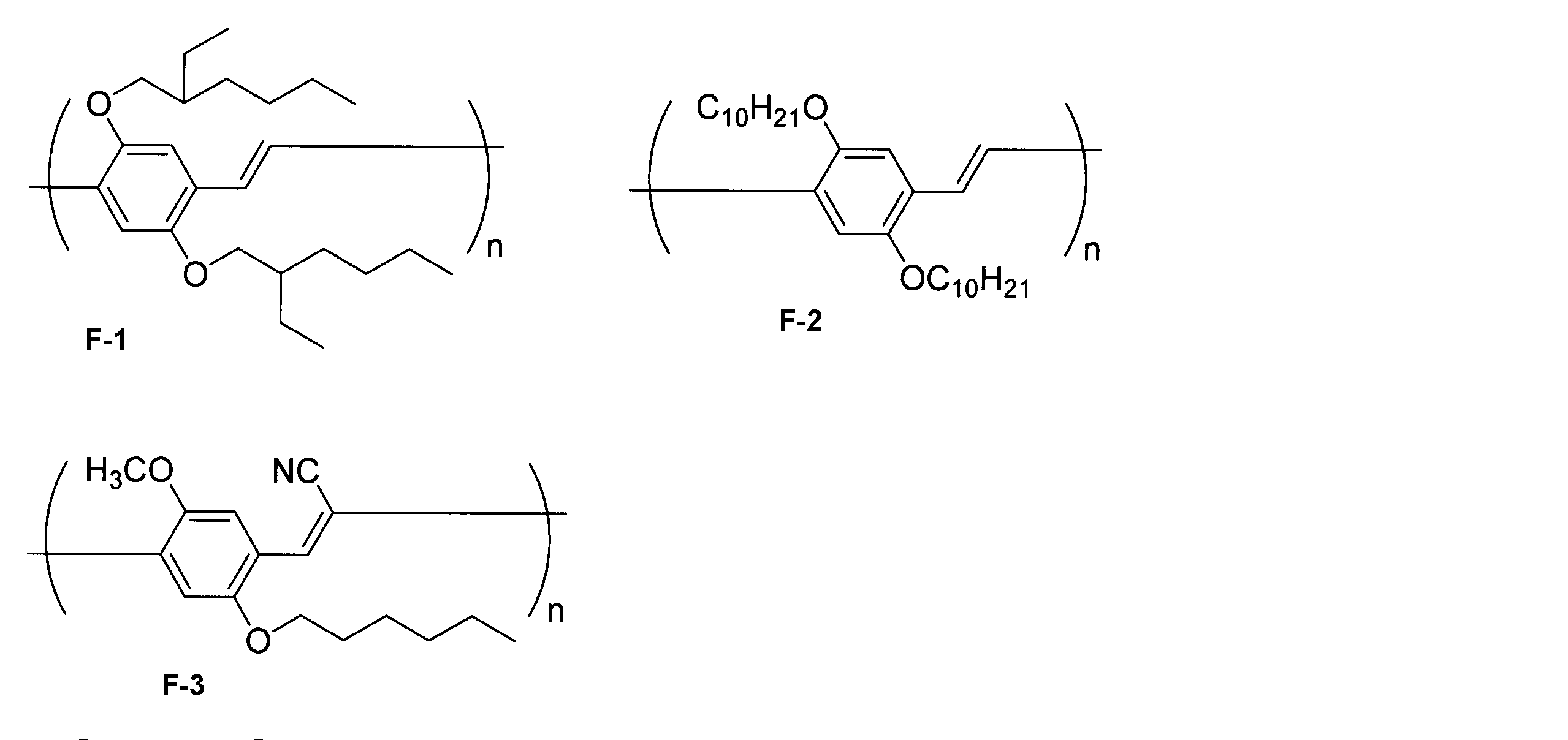
p-フェニレンエチニレン系化合物及びその誘導体から導かれる繰り返し単位を有する共役系高分子としては、下記の化合物が例示できる。なお下記式中、nは10以上の整数を示す。

上記以外の化合物及びその誘導体から導かれる繰り返し単位を有する共役系高分子としては、下記の化合物が例示できる。なお下記式中、nは10以上の整数を示す。

上記共役系高分子のなかでも、直鎖状の共役系高分子を用いることが好ましい。このような直鎖状の共役系高分子は、例えば、ポリチオフェン系高分子、ポリピロール系高分子の場合、各モノマーのチオフェン環又はピロール環が、それぞれ2,5位で結合することにより得られる。ポリ-p-フェニレン系高分子、ポリ-p-フェニレンビニレン系高分子、ポリ-p-フェニレンエチニレン系高分子では、各モノマーのフェニレン基がパラ位(1,4位)で結合することにより得られる。
本発明で用いる導電性高分子は、上述の繰り返し単位(以下、この繰り返し単位を与えるモノマーを「第1のモノマー(群)」とも称する)を1種単独で有しても、2種以上を組合わせて有していてもよい。また、第1のモノマーに加えて、他の構造を有するモノマー(以下、「第2のモノマー」と称する)から誘導される繰り返し単位を、併せて有していてもよい。複数種の繰り返し単位からなる高分子の場合、ブロック共重合体であっても、ランダム共重合体であっても、グラフト重合体であってもよい。
上記第1のモノマーと併用される、他の構造を有する第2のモノマーとしては、フルオレニレン基、カルバゾール基、ジベンゾ[b,d]シロール基、チエノ[3,2-b]チオフェン基、チエノ[2,3-c]チオフェン基、ベンゾ[1,2-b;4,5-b’]ジチオフェン基、シクロペンタ[2,1-b;3,4-b’]ジチオフェン基、ピロロ[3,4-c]ピロール-1,4(2H,5H)-ジオン基、ベンゾ[2,1,3]チアジアゾール-4,8-ジイル基、アゾ基、1,4-フェニレン基、5H-ジベンゾ[b、d]シロール基、チアゾール基、イミダゾール基、ピロロ[3,4-c]ピロール-1,4(2H、5H)-ジオン基、オキサジアゾール基、チアジアゾール基、トリアゾール基等を有する化合物、及びこれらの化合物にさらに置換基を導入した誘導体が挙げられる。導入する置換基としては、上述した置換基と同様のものが挙げられる。
本発明で用いる導電性高分子は、第1のモノマー群から選択された1種又は複数種のモノマーから誘導される繰り返し単位を導電性高分子中、合計で50質量%以上有していることが好ましく、70質量%以上有していることがより好ましく、第1のモノマー群から選択された1種又は複数種のモノマーから誘導される繰り返し単位のみからなることが更に好ましい。特に好ましくは、第1のモノマー群から選択された単一の繰り返し単位のみからなる共役系高分子である。
第1のモノマー群のなかでも、チオフェン系化合物及び/又はその誘導体から誘導される繰り返し単位を含むポリチオフェン系高分子がより好ましく用いられる。特に、下記の構造式(1)~(5)で表されるチオフェン環、又はチオフェン環含有縮合芳香環構造を繰り返し単位として有するポリチオフェン系高分子が好ましい。

上記構造式(1)~(5)中、R1~R13はそれぞれ独立に水素原子、ハロゲン原子、アルキル基、アルコキシ基、パーフルオロアルキル基、パーフルオロアルコキシ基、アミノ基、アルキルチオ基、ポリアルキレンオキシ基、アシルオキシ基又はアルキルオキシカルボニル基を表し、Yは炭素原子、窒素原子又はケイ素原子を表し、nは1または2の整数を表す。また*は、各繰り返し単位の連結部位を表す。
導電性高分子の分子量は特に限定されず、高分子量のものはもちろん、それ未満の分子量のオリゴマー(例えば重量平均分子量1000~10000程度)であってもよい。
高い導電性を実現する観点から、導電性高分子は、酸、光、熱に対して分解されにくいものが好ましい。高い導電性を得るためには、導電性高分子の長い共役鎖を介した分子内のキャリア伝達、及び分子間のキャリアホッピングが必要となる。そのためには、導電性高分子の分子量がある程度大きいことが好ましく、この観点から、本発明で用いる導電性高分子の分子量は、重量平均分子量で5000以上であることが好ましく、7000~300,000であることがより好ましく、8000~100,000であることがさらに好ましい。当該重量平均分子量は、ゲル浸透クロマトグラフィー(GPC)により測定できる。
高い導電性を実現する観点から、導電性高分子は、酸、光、熱に対して分解されにくいものが好ましい。高い導電性を得るためには、導電性高分子の長い共役鎖を介した分子内のキャリア伝達、及び分子間のキャリアホッピングが必要となる。そのためには、導電性高分子の分子量がある程度大きいことが好ましく、この観点から、本発明で用いる導電性高分子の分子量は、重量平均分子量で5000以上であることが好ましく、7000~300,000であることがより好ましく、8000~100,000であることがさらに好ましい。当該重量平均分子量は、ゲル浸透クロマトグラフィー(GPC)により測定できる。
これらの導電性高分子は、構成単位である上記モノマーを通常の酸化重合法により重合させて製造できる。
また、市販品を用いることもでき、例えば、アルドリッチ社製のポリ(3-ヘキシルチオフェン-2,5ージイル) レジオレギュラー品が挙げられる。
また、市販品を用いることもでき、例えば、アルドリッチ社製のポリ(3-ヘキシルチオフェン-2,5ージイル) レジオレギュラー品が挙げられる。
(C)オニウム塩化合物
本発明の導電性組成物はオニウム塩化合物を含有し、当該オニウム塩化合物により組成物の導電性を飛躍的に向上させることができる。導電性が向上するメカニズムの詳細はまだ定かではないが、該オニウム化合物が、上記CNT及び/又は導電性高分子に対し、そのままの状態で、又は光や熱などのエネルギーを外部から付与し活性化させた状態で、酸化能を発現する。このような酸化の過程で酸を発生し、発生した酸がドーパントとして作用するものと考えられる。ドーパントによって、導電性高分子、及び導電性高分子とCNT間の電荷移動がよりスムーズになるため、導電性が向上する。
従来のドーピング手法では、プロトン酸やルイス酸などの酸をドーパントとして用いるため、組成物中に酸を添加した時点でCNTや導電性高分子が凝集・析出・沈殿を生じてしまう。このような組成物では塗布性や成膜性が劣り、その結果、導電性も低下していた。
本発明のオニウム塩化合物は中性であり、CNTや導電性高分子を凝集・析出・沈殿させることがない。また、光や熱などのエネルギー付与により酸が発生する化合物でもあり、酸発生の開始時期をコントロールすることができる。酸を発生させない条件下で組成物を調製して凝集を防止し、良好な分散性・塗布性を維持したまま当該組成物を成形することができる。そのため、成形・成膜後に適宜エネルギー付与を行うことで、高い導電性を付与できる。
本発明の組成物は導電性高分子によりCNTの分散性向上を実現するものであるが、オニウム塩化合物は、これらと共に用いても、良好な分散性及び塗布性を維持することができる。塗布後の膜質も良好であり、CNT、導電性高分子、オニウム塩化合物が均一に分散されているため、塗布後に必要応じ、熱や光などの外部エネルギーを与えることで、高い導電性を示す。
上記の理由から、本発明で用いるオニウム塩化合物は、CNT及び/又は導電性高分子に対し、酸化能を有する化合物であることが好ましい。さらに、本発明で用いるオニウム塩化合物は、光や熱などのエネルギーの付与により酸を発生する化合物(酸発生剤)であることが好ましい。エネルギー付与の方法としては、活性エネルギー線の照射や加熱が挙げられる。
このようなオニウム塩化合物として、スルホニウム塩、ヨードニウム塩、アンモニウム塩、カルボニウム塩、ホスホニウム塩等が挙げられる。なかでも、スルホニウム塩、ヨードニウム塩、アンモニウム塩、カルボニウム塩が好ましく、スルホニウム塩、ヨードニウム塩、カルボニウム塩がより好ましく、スルホニウム塩、ヨードニウム塩が特に好ましい。当該塩を構成するアニオン部分としては、強酸の対アニオンが挙げられる。
具体的には、スルホニウム塩としては下記一般式(I)及び(II)で表される化合物が、ヨードニウム塩としては下記一般式(III)で表される化合物が、アンモニウム塩としては下記一般式(IV)で表される化合物が、カルボニウム塩としては下記一般式(V)で表される化合物がそれぞれ挙げられ、本発明において好ましく用いられる。
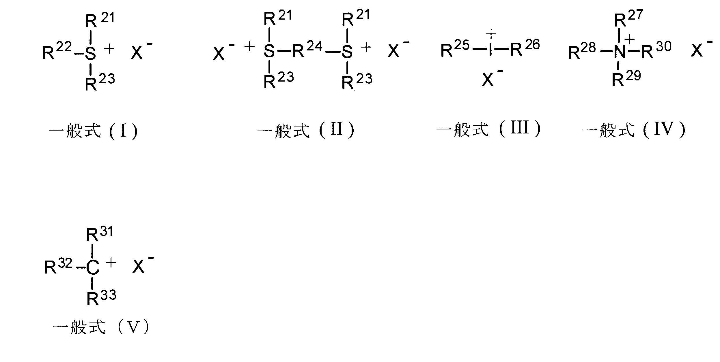
上記一般式(I)~(V)中、R21~R23、R25~R26及びR31~R33は、それぞれ独立に直鎖、分岐又は環状のアルキル基、アラルキル基、アリール基、芳香族へテロ環基を表す。R27~R30は、それぞれ独立に水素原子、直鎖、分岐又は環状のアルキル基、アラルキル基、アリール基、芳香族へテロ環基、アルコキシ基、アリールオキシ基を表す。R24は、直鎖、分岐又は環状のアルキレン基、アリーレン基を示す。R21~R33は、さらに置換されていてもよい。X-は、強酸のアニオンを表す。
一般式(I)においてR21~R23のいずれか2つの基が、一般式(II)においてR21及びR23が、一般式(III)においてR25及びR26が、一般式(IV)においてR27~R30のいずれか2つの基が、一般式(V)においてR31~R33のいずれか2つの基が、それぞれ結合して脂肪族環、芳香族環、ヘテロ環を形成してもよい。
一般式(I)においてR21~R23のいずれか2つの基が、一般式(II)においてR21及びR23が、一般式(III)においてR25及びR26が、一般式(IV)においてR27~R30のいずれか2つの基が、一般式(V)においてR31~R33のいずれか2つの基が、それぞれ結合して脂肪族環、芳香族環、ヘテロ環を形成してもよい。
R21~R23、R25~R33において、直鎖又は分岐のアルキル基としては、炭素数1~20のアルキル基が好ましく、具体的には、メチル基、エチル基、プロピル基、n-ブチル基、sec-ブチル基、t-ブチル基、ヘキシル基、オクチル基、ドデシル基などが挙げられる。
環状アルキル基としては、炭素数3~20のアルキル基が好ましく、具体的には、シクロプロピル基、シクロペンチル基、シクロヘキシル基、ビシクロオクチル基、ノルボルニル基、アダマンチル基などが挙げられる。
アラルキル基としては、炭素数7~15のアラルキル基が好ましく、具体的には、ベンジル基、フェネチル基などが挙げられる。
アリール基としては、炭素数6~20のアリール基が好ましく、具体的には、フェニル基、ナフチル基、アントラニル基、フェナンシル基、ピレニル基などが挙げられる。
芳香族へテロ環基としては、ピリジル基、ピラゾール基、イミダゾール基、ベンゾイミダゾール基、インドール基、キノリン基、イソキノリン基、プリン基、ピリミジン基、オキサゾール基、チアゾール基、チアジン基等が挙げられる。
R27~R30において、アルコキシ基としては、炭素数1~20の直鎖又は分岐のアルコキシ基が好ましく、具体的には、メトキシ基、エトキシ基、iso-プロポキシ基、ブトキシ基、ヘキシルオキシ基などが挙げられる。
アリールオキシ基としては、炭素数6~20のアリールオキシ基が好ましく、具体的には、フェノキシ基、ナフチルオキシ基などが挙げられる。
アリールオキシ基としては、炭素数6~20のアリールオキシ基が好ましく、具体的には、フェノキシ基、ナフチルオキシ基などが挙げられる。
R24において、アルキレン基としては、炭素数2~20のアルキレン基が好ましく、具体的には、エチレン基、プロピレン基、ブチレン基、へキシレン基などが挙げられる。環状アルキレン基としては、炭素数3~20の環状アルキレン基が好ましく、具体的には、シクロペンチレン基、シクロへキシレン、ビシクロオクチレン基、ノルボニレン基、アダマンチレン基などが挙げられる。
アリーレン基としては、炭素数6~20のアリーレン基が好ましく、具体的には、フェニレン基、ナフチレン基、アントラニレン基などが挙げられる。
アリーレン基としては、炭素数6~20のアリーレン基が好ましく、具体的には、フェニレン基、ナフチレン基、アントラニレン基などが挙げられる。
R21~R33が更に置換基を有する場合、置換基として好ましくは、炭素数1~4のアルキル基、炭素数1~4のアルコキシ基、ハロゲン原子(フッ素原子、塩素原子、沃素原子)、炭素数6~10のアリール基、炭素数6~10のアリールオキシ基、炭素数2~6のアルケニル基、シアノ基、ヒドロキシル基、カルボキシ基、アシル基、アルコキシカルボニル基、アルキルカルボニルアルキル基、アリールカルボニルアルキル基、ニトロ基、アルキルスルホニル基、トリフルオロメチル基、-S-R41などが挙げられる。なお、R41は、前記R21と同義である。
X-としては、アリールスルホン酸のアニオン、パーフルオロアルキルスルホン酸のアニオン、過ハロゲン化ルイス酸のアニオン、パーフルオロアルキルスルホンイミドのアニオン、過ハロゲン酸アニオン、又は、アルキル若しくはアリールボレートアニオンが好ましい。これらは、さらに置換基を有してもよく、置換基としてはフルオロ基が挙げられる。
アリールスルホン酸のアニオンとして具体的には、p-CH3C6H4SO3 -、PhSO3 -、ナフタレンスルホン酸のアニオン、ナフトキノンスルホン酸のアニオン、ナフタレンジスルホン酸のアニオン、アントラキノンスルホン酸のアニオンが挙げられる。
パーフルオロアルキルスルホン酸のアニオンとして具体的には、CF3SO3 -、C4F9SO3 -、C8F17SO3 -が挙げられる。
過ハロゲン化ルイス酸のアニオンとして具体的には、PF6 -、SbF6 -、BF4 -、AsF6 -、FeCl4 -が挙げられる。
パーフルオロアルキルスルホンイミドのアニオンとして具体的には、CF3SO2-N--SO2CF3、C4F9SO2-N--SO2C4F9が挙げられる。
過ハロゲン酸アニオンとして具体的には、ClO4 -、BrO4 -、IO4 -が挙げられる。
アルキル若しくはアリールボレートアニオンとして具体的には、(C6H5)4B-、(C6F5)4B-、(p-CH3C6H4)4B-、(C6H4F)4B-が挙げられる。
X-としてより好ましくは、過ハロゲン化ルイス酸のアニオン、フルオロ基が置換したアルキル若しくはアリールボレートアニオンであり、さらに好ましくはフルオロ置換アリールボレートアニオンであり、特に好ましくはペンタフルオロフェニルボレートアニオンである。
オニウム塩の具体例を以下に示すが、本発明はこれらに限定されるものではない。


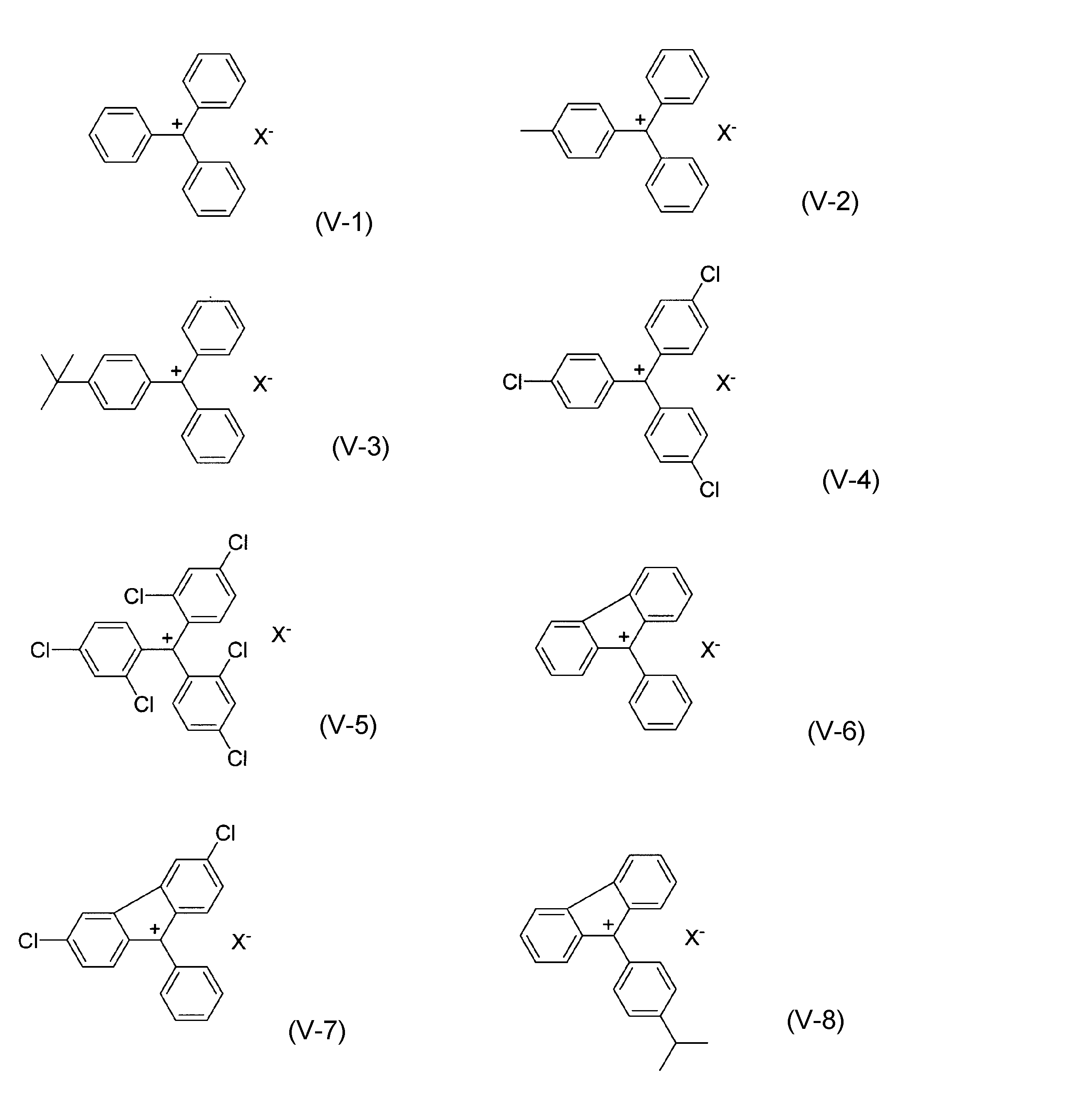
なお、上記具体例中のX-は、PF6
-、SbF6
-、CF3SO3
-、CH3PhSO3
-、BF4
-、(C6H5)4B-、RfSO3
-、(C6F5)4B-、又は下記式で表されるアニオン

を表し、Rfは任意の置換基を有するパーフルオロアルキル基を示す。
本発明においては、特に下記一般式(VI)又は(VII)で表されるオニウム塩化合物が好ましい。

一般式(VI)中、Yは炭素原子又は硫黄原子を表し、Ar1はアリール基を表し、Ar2~Ar4は、それぞれ独立にアリール基、芳香族へテロ環基を表す。Ar1~Ar4は、さらに置換されていてもよい。
Ar1としては、好ましくはフルオロ置換アリール基であり、より好ましくはペンタフルオロフェニル基、又は少なくとも1つのパーフルオロアルキル基で置換されたフェニル基であり、特に好ましくはペンタフルオロフェニル基である。
Ar2~Ar4のアリール基、芳香族へテロ環基は、上述のR21~R23、R25~R33のアリール基、芳香族へテロ環基と同義であり、好ましくはアリール基であり、より好ましくはフェニル基である。これらの基は、さらに置換されていてもよく、置換基としては上述のR21~R33の置換基が挙げられる。
Ar1としては、好ましくはフルオロ置換アリール基であり、より好ましくはペンタフルオロフェニル基、又は少なくとも1つのパーフルオロアルキル基で置換されたフェニル基であり、特に好ましくはペンタフルオロフェニル基である。
Ar2~Ar4のアリール基、芳香族へテロ環基は、上述のR21~R23、R25~R33のアリール基、芳香族へテロ環基と同義であり、好ましくはアリール基であり、より好ましくはフェニル基である。これらの基は、さらに置換されていてもよく、置換基としては上述のR21~R33の置換基が挙げられる。
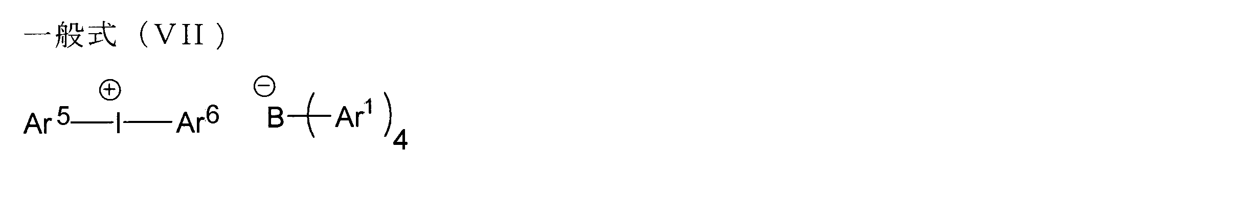
一般式(VII)中、Ar1はアリール基を表し、Ar5及びAr6は、それぞれ独立にアリール基、芳香族へテロ環基を表す。Ar1、Ar5及びAr6は、さらに置換されていてもよい。
Ar1は、上記一般式(VI)のAr1と同義であり、好ましい範囲も同様である。
Ar5及びAr6は、上記一般式(VI)のAr2~Ar4と同義であり、好ましい範囲も同様である。
Ar1は、上記一般式(VI)のAr1と同義であり、好ましい範囲も同様である。
Ar5及びAr6は、上記一般式(VI)のAr2~Ar4と同義であり、好ましい範囲も同様である。
上記オニウム塩化合物は、通常の化学合成により製造することができる。また、市販の試薬等を用いることもできる。
オニウム塩化合物の合成方法の一実施態様を下記に示すが、本発明はこれに限定されるものではない。他のオニウム塩に関しても、同様の手法により合成する事ができる。
トリフェニルスルホニウムブロミド(東京化成製)2.68g、リチウム テトラキス(ペンタフルオロフェニル)ボレート-エチルエ-テルコンプレックス(東京化成製)5.00g、およびエタノール146mlを500ml容三口フラスコに入れ、室温にて2時間撹拌した後、純水200mlを添加し、析出した白色固形物を濾過により分取する。この白色固体を純水およびエタノールにて洗浄および真空乾燥することにより、オニウム塩としてトリフェニルスルホニウム テトラキス(ペンタフルオロフェニル)ボレート6.18gを得ることができる。
オニウム塩化合物は、1種類単独で又は2種類以上を組み合わせて使用することができる。
[溶媒]
本発明の導電性組成物は、CNT、導電性高分子及びオニウム塩化合物に加えて、溶媒を含有することが好ましい。
溶媒は、CNT、導電性高分子及びオニウム塩化合物を良好に分散又は溶解できればよく、水、有機溶媒、及びこれらの混合溶媒を用いることができる。好ましくは有機溶媒であり、アルコール、クロロホルムなどのハロゲン系溶媒、DMF、NMP、DMSOなどの非プロトン性の極性溶媒、クロロベンゼン、ジクロロベンゼン、ベンゼン、トルエン、キシレン、メシチレン、テトラリン、テトラメチルベンゼン、ピリジンなどの芳香族系溶媒、シクロヘキサノン、アセトン、メチルエチルケントンなどのケトン系溶媒、ジエチルエーテル、THF、t-ブチルメチルエーテル、ジメトキシエタン、ジグライムなどのエーテル系溶媒などが好ましく、クロロホルムなどのハロゲン系溶媒、DMF、NMPなどの非プロトン性の極性溶媒、ジクロロベンゼン、キシレン、テトラリン、テトラメチルベンゼンなどの芳香族系溶媒、THFなどのエーテル系溶媒等がより好ましい。
また、溶媒は、あらかじめ脱気しておくことが好ましい。溶媒中における溶存酸素濃度を、10ppm以下とすることが好ましい。脱気の方法としては、減圧下超音波を照射する方法、アルゴン等の不活性ガスをバブリングする方法などが挙げられる。
さらに、溶媒は、あらかじめ脱水しておくことが好ましい。溶媒中における水分量を、1000ppm以下とすることが好ましく、100ppm以下とすることがより好ましい。脱水の方法としては、モレキュラーシーブを用いる方法、蒸留など、公知の方法を用いることができる。
[他の成分]
本発明の導電性組成物は、上記の各成分に加えて、他の成分を含んでいてもよい。
例えば、分散安定性を向上させるために、水酸化リチウム、過硫酸アンモニウム、紫外線吸収剤などを含有させることができる。また、膜強度を高める観点からは、無機微粒子、ポリマー微粒子、シランカップリング剤などを、屈折率を下げて透明性を高める観点からは、フッ素系化合物などを、塗布時のムラを防ぐ観点からは、フッ素系界面活性剤などを、用途に応じて適宜含有させることができる。
これらの成分の含有量は、組成物全質量に対し、0.1~5質量%程度であることが好ましい。
本発明の導電性組成物は、上記の各成分に加えて、他の成分を含んでいてもよい。
例えば、分散安定性を向上させるために、水酸化リチウム、過硫酸アンモニウム、紫外線吸収剤などを含有させることができる。また、膜強度を高める観点からは、無機微粒子、ポリマー微粒子、シランカップリング剤などを、屈折率を下げて透明性を高める観点からは、フッ素系化合物などを、塗布時のムラを防ぐ観点からは、フッ素系界面活性剤などを、用途に応じて適宜含有させることができる。
これらの成分の含有量は、組成物全質量に対し、0.1~5質量%程度であることが好ましい。
[導電性組成物の調製]
本発明の導電性組成物は、CNT、導電性高分子及びオニウム塩化合物を含有し、必要に応じて溶媒を加えてなる。本発明の組成物は、溶媒にCNTが分散されたCNT分散液であることが好ましい。
本発明の組成物は、CNTの含有量を変えることによって、該組成物の電導性や半導体特性を制御することができる。組成物中のCNT、導電性高分子及びオニウム塩化合物の含有量は、組成物の用途、当該用途に求められる導電性や透明性などの特性に応じて、適宜選択・決定することができる。
組成物中のCNT含有量は、全固形分中、3~50質量%であることが好ましく、5~40質量%であることがより好ましく、10~30質量%であることがさらに好ましい。組成物中の導電性高分子含有量は、全固形分中、30~80質量%であることが好ましく、35~75質量%であることがより好ましく、40~70質量%であることがさらに好ましい。組成物中のオニウム塩化合物は、全固形分中、1~50質量%であることが好ましく、5~45質量%であることがより好ましく、10~40質量%であることがさらに好ましい。
溶媒を用いる場合、当該溶媒の使用量は、本発明の組成物の全固形分と溶媒の全重量に対し60~99.9質量%用いることが好ましく、70~99.5質量%用いることがより好ましく、80~99質量%用いることがさらに好ましい。
本発明の導電性組成物の調製は、上記の各成分を混合して調製することができる。好ましくは、溶媒にCNT、導電性高分子及びオニウム塩化合物を添加し、これらを通常の方法により分散させて調製する。各成分の添加・混合順序は特に限定されないが、予め溶媒中に導電性高分子を所定量添加した後、CNTを所定量添加することが好ましい。
調製方法に特に制限はなく、通常の方法を適用することができる。例えば、メカニカルホモジナイザー法、ジョークラッシャ法、超遠心粉砕法、カッティングミル法、自動乳鉢法、ディスクミル法、ボールミル法、超音波分散法などの分散方法を用いることができる。また、必要に応じ、これらの方法を2つ以上組み合わせて用いてもよい。好ましい分散方法の組み合わせは、メカニカルホモジナイザー法と超音波分散法である。組み合わせの順番はいかなるものであってもよく、順次異なる分散方法により分散する方法、もしくは同時に異なる分散方法で分散する方法がある。好ましくは、最初に弱い分散エネルギーを有する分散方法で分散した後、次に高い分散エネルギーを有する分散方法で分散する順番がよい。そうすることで、欠陥なく高い濃度でCNTを分散できるようになる。具体的には、最初にメカニカルホモジナイザー法、次に超音波分散法を組み合わせることが好ましい。
また、用いるオニウム塩化合物が熱や光等のエネルギー付与により酸を発生する化合物である場合、酸を生成しない温度下、放射線や電磁波等を遮った状態で、組成物の調製を行うこと好ましい。酸による凝集等を防ぎ、組成物の調製及び保存時において、組成物中の各成分の均一な分散性又は溶解性を保つことができる。
組成物の調製は、大気下で行うこともできるが、不活性雰囲気において行うことが好ましい。不活性雰囲気とは、酸素濃度が大気中濃度よりも少ない状態のことをいう。好ましくは、酸素濃度が10%以下の雰囲気である。不活性雰囲気にする方法としては、窒素、アルゴンなどの気体で大気を置換させる方法が挙げられ、好ましく用いられる。
また、調製時の温度は、0℃から50℃の範囲であることが好ましい。
また、調製時の温度は、0℃から50℃の範囲であることが好ましい。
得られた導電性組成物中に含まれるCNTには、欠陥のあるCNTが含まれていることがある。このようなCNTの欠陥は、組成物の導電性を低下させるため、低減化することが好ましい。組成物中のCNTの欠陥の量は、ラマンスペクトルのG-バンドとD-バンドの比率G/Dで見積もることができる。G/D比が高いほど欠陥の量が少ないCNT材料であると推定できる。本発明においては、組成物のG/D比が10以上であることが好ましく、30以上であることがより好ましい。
[導電性膜]
本発明の導電性膜は、前記導電性組成物を用いてなる。導電性膜の製造方法は、当該導電性組成物を成形するものであれば特に限定されない。好ましくは、導電性組成物を基材上に塗布して成膜する。
形成された導電性膜は、成形後さらに、熱や活性エネルギー線等のエネルギーを付与されることが好ましい。
本発明の導電性膜は、前記導電性組成物を用いてなる。導電性膜の製造方法は、当該導電性組成物を成形するものであれば特に限定されない。好ましくは、導電性組成物を基材上に塗布して成膜する。
形成された導電性膜は、成形後さらに、熱や活性エネルギー線等のエネルギーを付与されることが好ましい。
[成膜方法]
導電性膜の成膜方法は特に限定されず、例えば、スピンコート、エクストルージョンダイコート、ブレードコート、バーコート、スクリーン印刷、ステンシル印刷、ロールコート、カーテンコート、スプレーコート、ディップコート、インクジェット法など、公知の塗布方法を用いることができる。
塗布後は、必要に応じて乾燥工程を行う。例えば、熱風を吹き付けることにより溶媒を揮発、乾燥させることができる。
導電性膜の成膜方法は特に限定されず、例えば、スピンコート、エクストルージョンダイコート、ブレードコート、バーコート、スクリーン印刷、ステンシル印刷、ロールコート、カーテンコート、スプレーコート、ディップコート、インクジェット法など、公知の塗布方法を用いることができる。
塗布後は、必要に応じて乾燥工程を行う。例えば、熱風を吹き付けることにより溶媒を揮発、乾燥させることができる。
用いる導電性組成物の量は、所望の膜厚によって適宜調整される。導電性膜の膜厚は、用途に応じて適宜選択すればよい。例えば、透明電極に用いる場合は、抵抗値と光透過率が重要となる。LCD、PDP、EL素子等の表示装置用の透明電極の場合、好ましい抵抗値は、0.001~100,000Ω/□の範囲であり、より好ましくは0.1~10,000Ω/□の範囲である。光透過率は、550nmにおける光透過率が40%~100%程度、好ましくは50~100%、より好ましくは60~100%の範囲である。これらを満たすように、CNT、導電性高分子、オニウム塩化合物の濃度を考慮して膜厚を適宜調整する。
成膜後、当該膜に活性エネルギー線を照射又は加熱して、膜の導電性を向上させることが好ましい。
活性エネルギー線には、放射線や電磁波が包含され、放射線には粒子線(高速粒子線)と電磁放射線が包含される。粒子線としては、アルファ線(α線)、ベータ線(β線)、陽子線、電子線(原子核崩壊によらず加速器で電子を加速するものを指す)、重陽子線等の荷電粒子線、非荷電粒子線である中性子線、宇宙線等が挙げられ、電磁放射線としては、ガンマ線(γ線)、エックス線(X線、軟X線)が挙げられる。電磁波としては、電波、赤外線、可視光線、紫外線(近紫外線、遠紫外線、極紫外線)、X線、ガンマ線などがあげられる。本発明において用いる線種は特に限定されず、例えば、使用するオニウム塩化合物(酸発生剤)の極大吸収波長付近の波長を有する電磁波を適宜選べばよい。
これらの活性エネルギー線のうち、ドーピング効果および安全性の観点から好ましいのは紫外線、可視光線、赤外線であり、具体的には240~1100nm、好ましくは240~850nm、より好ましくは240~670nmに極大発光波長を有する光線である。
活性エネルギー線の照射には、放射線または電磁波照射装置が用いられる。照射する放射線または電磁波の波長は特に限定されず、使用するオニウム塩化合物の感応波長に対応する波長領域の放射線または電磁波を照射できるものを選べばよい。
放射線または電磁波を照射できる装置としては、LEDランプ、高圧水銀ランプ、超高圧水銀ランプ、DeepUVランプ、低圧UVランプなどの水銀ランプ、ハライドランプ、キセノンフラッシュランプ、メタルハライドランプ、ArFエキシマランプ、KrFエキシマランプなどのエキシマランプ、極端紫外光ランプ、電子ビーム、X線ランプを光源とする露光装置がある。紫外線照射は、通常の紫外線照射装置、例えば、市販の硬化/接着/露光用の紫外線照射装置(ウシオ電機株式会社SP9-250UBなど)を用いて行うことができる。
放射線または電磁波を照射できる装置としては、LEDランプ、高圧水銀ランプ、超高圧水銀ランプ、DeepUVランプ、低圧UVランプなどの水銀ランプ、ハライドランプ、キセノンフラッシュランプ、メタルハライドランプ、ArFエキシマランプ、KrFエキシマランプなどのエキシマランプ、極端紫外光ランプ、電子ビーム、X線ランプを光源とする露光装置がある。紫外線照射は、通常の紫外線照射装置、例えば、市販の硬化/接着/露光用の紫外線照射装置(ウシオ電機株式会社SP9-250UBなど)を用いて行うことができる。
露光時間及び光量は、用いるオニウム塩化合物の種類及びドーピング効果を考慮して適宜選択すればよい。具体的には、光量10mJ/cm2~10J/cm2、好ましくは50mJ/cm2~5J/cm2、で行うことが挙げられる。
加熱によるドーピングは、導電性組成物を塗布した基材(成膜)を、オニウム塩化合物が酸を発生する温度以上で加熱すればよい。加熱温度として、好ましくは50℃~200℃、より好ましくは70℃~150℃である。加熱時間は、好ましくは1分~60分、より好ましくは3分~30分である。
[基材]
基材は、本発明の導電性膜を成膜した後の用途等に応じ選択することができる。例えば、本発明の導電性膜をLCD、電気泳動方式表示材料、電子ペーパー、有機EL素子などの表示装置の電極として形成する場合は、ガラス基板またはプラスチック基板を好適に用いることができる。また、導電性膜との間に絶縁膜を設けた金属基板を使用することもできる。なお、基材は板状に限らず、例えば、表面が曲面であるものや、凹凸が形成されているものなど、用途に応じて選択することができる。また、本発明の導電性膜を熱電変換用途に用いる場合には、導電性膜の圧着面に各種電極材料を設けた基材を好適に用いることができる。この電極材料としてはITO、ZnO等の透明電極、銀、銅、金、アルミニウムなどの金属電極、CNT、グラフェンなどの炭素材料、PEDOT/PSS等の有機材料、銀、カーボンなどの導電性微粒子を分散した導電性ペースト、銀、銅、アルミニウムなどの金属ナノワイヤーを含有する導電性ペースト等が使用できる。
基材は、本発明の導電性膜を成膜した後の用途等に応じ選択することができる。例えば、本発明の導電性膜をLCD、電気泳動方式表示材料、電子ペーパー、有機EL素子などの表示装置の電極として形成する場合は、ガラス基板またはプラスチック基板を好適に用いることができる。また、導電性膜との間に絶縁膜を設けた金属基板を使用することもできる。なお、基材は板状に限らず、例えば、表面が曲面であるものや、凹凸が形成されているものなど、用途に応じて選択することができる。また、本発明の導電性膜を熱電変換用途に用いる場合には、導電性膜の圧着面に各種電極材料を設けた基材を好適に用いることができる。この電極材料としてはITO、ZnO等の透明電極、銀、銅、金、アルミニウムなどの金属電極、CNT、グラフェンなどの炭素材料、PEDOT/PSS等の有機材料、銀、カーボンなどの導電性微粒子を分散した導電性ペースト、銀、銅、アルミニウムなどの金属ナノワイヤーを含有する導電性ペースト等が使用できる。
塗布、成膜後に加熱や光照射を行う場合は、これらの刺激による影響を受けにくい基材を選択することが好ましい。本発明で使用可能な基材としては、ガラス、透明セラミックス、金属、プラスチックフィルムなどの基板が挙げられる。ガラス、透明セラミックスは、金属、プラスチックフィルムに比べ、柔軟性に欠ける。また、金属とプラスチックフィルムを価格的に比べると、プラスチックフィルムの方が安価であり、柔軟性を有するので好ましい。
このような観点から、本発明の基材としては、ポリエステル系樹脂、ポリイミド、ポリカーボネート、ポリプロピレン、ポリエーテルスルホン、シクロオレフィンポリマーなどのプラスチックフィルム(樹脂フィルム)が好ましく、特に、ポリエステル系樹脂(以下、適宜、「ポリエステル」と称する)が好ましい。ポリエステルとしては、芳香族二塩基酸又はそのエステル形成性誘導体とジオール又はそのエステル形成性誘導体とから合成される線状飽和ポリエステルが好ましい。
このような観点から、本発明の基材としては、ポリエステル系樹脂、ポリイミド、ポリカーボネート、ポリプロピレン、ポリエーテルスルホン、シクロオレフィンポリマーなどのプラスチックフィルム(樹脂フィルム)が好ましく、特に、ポリエステル系樹脂(以下、適宜、「ポリエステル」と称する)が好ましい。ポリエステルとしては、芳香族二塩基酸又はそのエステル形成性誘導体とジオール又はそのエステル形成性誘導体とから合成される線状飽和ポリエステルが好ましい。
本発明に用い得るポリエステルの具体例としては、ポリエチレンテレフタレート、ポリエチレンイソフタレート、ポリエチレンナフタレート、ポリブチレンテレフタレート、ポリ(1,4-シクロヘキシレンジメチレンテレフタレート)、ポリエチレン-2,6-フタレンジカルボキシレート等が挙げられる。このうち、入手の容易性、経済性及び効果の観点から、ポリエチレンテレフタレート、ポリエチレンナフタレート等が好ましい。
また、本発明の効果を損なわない限りにおいて、上記樹脂の共重合体、又はこれらの樹脂と他の種類の樹脂とのブレンド物なども用いることができる。
更に、このポリエステルフィルムの中には、滑り性を良くするために少量の無機又は有機の微粒子、たとえば、酸化チタン、炭酸カルシュウム、シリカ、硫酸バリュウム、シリコーン等の如き無機フィラー、アクリル、ベンゾグアナミン、テフロン(登録商標)、エポキシ等の如き有機フィラー、ポリエチレングリコール(PEG)、ドデシルベンゼンスルホン酸ソーダ等の接着性向上剤や帯電防止剤を含有させることができる。
本発明に用いるポリエステルフィルムは、前記のポリエステル樹脂を溶融押出しでフィルム状にし、縦及び横二軸延伸による配向結晶化及び熱処理による結晶化させることにより形成し得る。これらフィルムの製造方法は、公知の方法や条件を適宜選択して用いることができる。
ここで用いられるポリエステルフィルムの厚さに特に制限はなく、フィルムの使用目的に応じて適宜選択できるが、一般的には、5~500μmのものを用いることが好ましい。
基材は、さらに紫外線吸収剤等の添加剤を含むことが好ましい。紫外線吸収剤としては、オキサゾール系、トリアジン系、スチルベン系、クマリン系吸収剤を好適に用いることができる。
本発明では、必要に応じて、基材に前処理を施してもよい。例えば、コロナ処理、プラズマ処理、UVオゾン処理、EB照射処理等、公知の前処理方法を用いることができる。これらの処理により基材表面に極性を持つ水酸基、カルボキシル基又は塩基性基等を生成させることができ、導電性膜との密着性が向上する。あるいは、導電性膜との密着性の向上を図るため、基材上に易接着層を設けることができる。
易接着層としては、ゼラチン、ポリアクリル酸、ポリアクリレート、スチレン-ブタジエン共重合体(以下、適宜、「SBR」と略称する)、水系ウレタン樹脂などが挙げられる。さらに、架橋剤とを含有する構成であってもよい。
易接着層としては、ゼラチン、ポリアクリル酸、ポリアクリレート、スチレン-ブタジエン共重合体(以下、適宜、「SBR」と略称する)、水系ウレタン樹脂などが挙げられる。さらに、架橋剤とを含有する構成であってもよい。
スチレン-ブタジエン共重合体はラテックスであることが好ましい。具体的には、日本ゼオン社からニポール(商品名)として、住友ノーガタック社からノーガテックス(商品名)として、武田薬品工業社からクロスレン(商品名)として、旭ダウ社から旭ダウラテックス(商品名)として、その他に大日本インキ化学工業社や海外メーカーから販売されている市販品を用いることもできる。
ラテックスの場合、分散体粒子の粒径は5μm以下が好ましく、1μm以下がより好ましく、0.2μm以下が更に好ましい。粒子径が大きい場合には、塗布工程で粒子の凝集が生じやすかったり、フィルムの透明性、光沢などが不良になったりする問題がある。更に塗布層の厚さを薄くする必要がある場合には、それに応じて粒径を小さくする必要がある。
スチレン-ブタジエン共重合体におけるスチレン/ブタジエンの含有比率は50/50~80/20程度であることが好ましい。ラテックス中に含まれるSBRの割合は、固型分重量として30~50重量%であることが好ましい。
また、この易接着層には架橋剤が添加されてもよいが、架橋剤としてはトリアジン系架橋剤が好ましい。
[導電性積層体、導電性物品]
上記の手順で製造された導電性膜は、導電性フィルムとして用いることもできるし、基材上に塗布したまま、導電性積層体として用いることもできる。導電性積層体は、さらに電極等を有していてもよい。
本発明の導電性膜は、CNTの分散性に優れ、かつ含有するCNTに欠陥が少ないという利点を有し、CNT、導電性高分子、オニウム塩化合物の種類や含有量等を適宜調整することにより、10~2000 S/cm程度の高い導電率を実現できる。そのため、本発明の導電性組成物、導電性膜、導電性積層体は、各種導電性物品への幅広い適用が可能である。例えば、LCD、PDP、EL素子などの薄型のディスプレイ、太陽電池、タッチパネルなどの電極、コンデンサ、キャパシタ、二次電池などの導電材料、光電変換素子、圧電変換素子、熱電変換素子などの有機半導体材料、調光素子用材料、帯電防止用材料等に好適に用いることができる。
[熱電変換素子]
本発明の導電性組成物は高い導電性に加えて優れた熱電変換性能を有し、熱電変換材料として好適に用いることができる。当該組成物を用いてなる導電性膜は熱電変換素子の熱電変換層として、また、基板上に導電性膜及び電極を備えた導電性積層体は、熱電変換素子として用いることができる。
熱電変換材料や素子の熱電変換性能は、下記式(A)で示される性能指数ZTにより表され、性能向上には熱起電力及び導電率を高めることが重要である。本発明の組成物は、熱起電力を低下させることなく高い導電性を実現できる。
性能指数ZT=S2・σ・T/κ (A)
S(V/K):熱起電力(ゼーベック係数) σ(S/m):導電率
κ(W/mK):熱伝導率 T(K):絶対温度
本発明の熱電変換素子は、本発明の導電性膜、又は本発明の導電性積層体を備えるものであればよく、その構成については特に限定されないが、基材と、本発明の導電性膜を含む熱電変換層と、これらを電気的に接続する電極とを有していることが好ましい。
本発明の熱電変換素子の構造の一例として、図1に示す素子(1)及び図2に示す素子(2)の構造が挙げられる。図1に示す素子(1)は、第1の基材(12)上に、第1の電極(13)及び第2の電極(15)を含む一対の電極と、該電極間に熱電変換層(14)として本発明の導電性膜を備える素子である。第2の電極(15)は第2の基材(16)表面に配設されており、第1の基材(12)及び第2の基材(16)の外側には互いに対向して金属板(17)が配設される。図2に示す素子(2)は、第1の基材(22)上に、第1の電極(23)及び第2の電極(25)が配設され、その上に熱電変換材料層(24)として本発明の導電性膜が設けられている。図1及び2中、矢印は、熱電変換素子の使用時における温度差の方向を示す。
本発明の熱電変換素子は、本発明の導電性積層体を備えるものであってもよく、この場合には、本発明の導電性積層体を構成する基材を上記第1の基材(12、22)として機能させることが好ましい。すなわち、本発明の導電性積層体の基材表面(熱電変換材料との圧着面)には、上述した各種電極材料が設けられていることが好ましい。
形成された熱電変換材料層(導電性膜)は、一方の表面が基材で覆われているが、これを用いて熱電変換素子を調製するに際しては、他方の表面にも基材(第2の基材(16、26))を圧着させることが、膜の保護の観点から好ましい。また、この第2の基材(16)表面(熱電変換材料層との圧着面)には上記各種電極材料を予め設けておいてもよい。また、第2の基材と熱電変換材料層との圧着は、密着性向上の観点から100℃~200℃程度に加熱して行うことが好ましい。
本発明の熱電変換素子において、熱電変換層の膜厚は、0.1μm~1000μmであることが好ましく、1μm~100μmであることがより好ましい。膜厚が薄いと温度差を付与しにくくなることと、膜内の抵抗が増大してしまうため好ましくない。
また、第1及び第2の基材の厚さは取り扱い性、耐久性等の点から30~3000μmであることが好ましく、100~1000μmであることが好ましい。
一般に熱電変換素子では、有機薄膜太陽電池用素子等の光電変換素子と比べて、変換層の塗布・製膜が有機層1層分でよく、簡便に素子を製造できる。特に、本発明の熱電変換材料を用いると有機薄膜太陽電池用素子と比較して100倍~1000倍程度の厚膜化が可能であり、空気中の酸素や水分に対する化学的な安定性が向上する。
また、第1及び第2の基材の厚さは取り扱い性、耐久性等の点から30~3000μmであることが好ましく、100~1000μmであることが好ましい。
一般に熱電変換素子では、有機薄膜太陽電池用素子等の光電変換素子と比べて、変換層の塗布・製膜が有機層1層分でよく、簡便に素子を製造できる。特に、本発明の熱電変換材料を用いると有機薄膜太陽電池用素子と比較して100倍~1000倍程度の厚膜化が可能であり、空気中の酸素や水分に対する化学的な安定性が向上する。
[熱電発電体]
本発明の熱電発電体は、本発明の熱電変換素子を用いて熱電変換を行う物、装置、機械、器具等を含む。より具体的には、温泉熱発電機、太陽熱発電機、廃熱発電機等の発電機や、腕時計用電源、半導体駆動電源、小型センサー用電源等が挙げられる。
本発明の熱電発電体は、本発明の熱電変換素子を用いて熱電変換を行う物、装置、機械、器具等を含む。より具体的には、温泉熱発電機、太陽熱発電機、廃熱発電機等の発電機や、腕時計用電源、半導体駆動電源、小型センサー用電源等が挙げられる。
以下、実施例に基づき本発明をより詳しく説明するが、本発明はそれらに限定されるものではない。
実施例1
単層カーボンナノチューブとしてASP-100F(Hanwha nanotech社製、純度95%)10mg、及び下記に示す導電性高分子1 25mgに、クロロホルム10mLを加えて、メカニカルな攪拌装置で20分間攪拌した。その後、超音波洗浄機(井内盛栄堂(株)製US-2、出力120W、間接照射)を用いて、30℃で40分間超音波分散することによって、CNT分散クロロホルム溶液を得た。この溶液に、オニウム塩化合物として前記例示化合物(I-1)8mgを室温で添加して、導電性組成物のクロロホルム溶液を作製した。一方、基板として、1.1mmの厚み、40mm×50mmのガラス基板をアセトン中で超音波洗浄した後、10分間UV-オゾン処理を行った。上記導電性組成物のクロロホルム溶液をこのガラス基板上にスピンコート(1500rpm、30秒間)した後、室温真空条件で3時間乾燥することで、厚さ約50nmの導電膜を形成した。その後、必要に応じ、紫外線照射機(アイグラフィックス株式会社製、ECS-401GX)により紫外線照射(光量:200mJ/cm2)を行った。
得られた膜の導電率、成膜性、G/D比を、下記の手法で測定・評価した。結果を表1に示す。
[導電率の測定]
形成した導電膜の導電率は、「高抵抗率計:ハイレスタUP」または「低抵抗率計:ロレスタGP」(機器名、いずれも(株)三菱化学アナリテック製)を用い表面抵抗率(単位:Ω/□)を測定し、触針型膜厚計により膜厚(単位:cm)を測定し、下記式より導電率(S/cm)を算出した。
(導電率)=1/((表面抵抗)×(膜厚))
形成した導電膜の導電率は、「高抵抗率計:ハイレスタUP」または「低抵抗率計:ロレスタGP」(機器名、いずれも(株)三菱化学アナリテック製)を用い表面抵抗率(単位:Ω/□)を測定し、触針型膜厚計により膜厚(単位:cm)を測定し、下記式より導電率(S/cm)を算出した。
(導電率)=1/((表面抵抗)×(膜厚))
[成膜性]
成膜性は目視により下記の3段階の基準で評価した。
1:良好
2:凝集物が少しみられ、成膜性が低下した
3:凝集物が多く、成膜性が大きく低下した
成膜性は目視により下記の3段階の基準で評価した。
1:良好
2:凝集物が少しみられ、成膜性が低下した
3:凝集物が多く、成膜性が大きく低下した
[G/D比]
分散液のラマン分光測定スペクトル(波長633nm、堀場製作所製レーザラマン分光測定装置)の測定により、CNTの欠陥の程度をG-バンドとD-バンドのスペクトル強度比から、G/D比で評価した。G/D比が小さい程、CNTの欠陥が多い。
分散液のラマン分光測定スペクトル(波長633nm、堀場製作所製レーザラマン分光測定装置)の測定により、CNTの欠陥の程度をG-バンドとD-バンドのスペクトル強度比から、G/D比で評価した。G/D比が小さい程、CNTの欠陥が多い。
実施例2~19
導電性高分子及びオニウム塩化合物の種類を表1に示すように変更した以外は実施例1と同様にして、導電性膜を製造し評価した。結果を表1に示す。
導電性高分子及びオニウム塩化合物の種類を表1に示すように変更した以外は実施例1と同様にして、導電性膜を製造し評価した。結果を表1に示す。

実施例20
実施例1においてオニウム塩化合物の種類を表1に示すように変更し、メカニカルな攪拌20分間と、その後の超音波洗浄機(井内盛栄堂(株)製US-2、出力120W、間接照射)攪拌40分間との代わりに、超音波破砕機(東京理化器械(株)製VCX-502、出力250W、直接照射)30分間攪拌にてCNT分散液を調製した以外は実施例1と同様にして、ガラス基板上に導電性膜を作製した。この塗膜を、実施例1と同様の手法により、導電率、成膜性、G/D比を評価した。
実施例1においてオニウム塩化合物の種類を表1に示すように変更し、メカニカルな攪拌20分間と、その後の超音波洗浄機(井内盛栄堂(株)製US-2、出力120W、間接照射)攪拌40分間との代わりに、超音波破砕機(東京理化器械(株)製VCX-502、出力250W、直接照射)30分間攪拌にてCNT分散液を調製した以外は実施例1と同様にして、ガラス基板上に導電性膜を作製した。この塗膜を、実施例1と同様の手法により、導電率、成膜性、G/D比を評価した。
実施例21
実施例1においてオニウム塩化合物の種類を表1に示すように変更し、CNT、導電性高分子、オニウム塩化合物の添加量をそれぞれ7.5mg、18.5mg、17mgに変えた以外は実施例1と同様にして、ガラス基板上に導電性膜を作製した。この塗膜を、実施例1と同様の手法により、導電率、成膜性、G/D比を評価した。
実施例1においてオニウム塩化合物の種類を表1に示すように変更し、CNT、導電性高分子、オニウム塩化合物の添加量をそれぞれ7.5mg、18.5mg、17mgに変えた以外は実施例1と同様にして、ガラス基板上に導電性膜を作製した。この塗膜を、実施例1と同様の手法により、導電率、成膜性、G/D比を評価した。
比較例1~5
実施例1においてオニウム塩化合物を添加する代わりに、無添加または表2に示す他のドーパント化合物を添加すること以外は実施例1と同様にして、ガラス基板上にCNTと導電性高分子とを含む比較用塗膜を作製した。この塗膜を、実施例1と同様の手法により、導電率、成膜性、G/D比を評価した。
実施例1においてオニウム塩化合物を添加する代わりに、無添加または表2に示す他のドーパント化合物を添加すること以外は実施例1と同様にして、ガラス基板上にCNTと導電性高分子とを含む比較用塗膜を作製した。この塗膜を、実施例1と同様の手法により、導電率、成膜性、G/D比を評価した。


表1から明らかなように、CNT、導電性高分子及びオニウム塩化合物を含有する組成物を用いて成形された実施例1~21の導電性膜では、高い導電率と、良好な成膜性を示した。また、実施例1~19及び21では、CNTの欠陥も少なかった。
これに対し、表2に示すオニウム塩化合物を用いていない比較例1~5では、導電率が大きく低下した。さらに、酸や金属ハロゲンといった従来のドーパントを用いた比較例3~5では、成膜性に劣る結果となった。
これに対し、表2に示すオニウム塩化合物を用いていない比較例1~5では、導電率が大きく低下した。さらに、酸や金属ハロゲンといった従来のドーパントを用いた比較例3~5では、成膜性に劣る結果となった。
実施例22
(熱電変換層の成膜)
厚さ300μmのニトフロンNo.901UL(日東電工社製品名)と両面粘着フイルムを用い、ガラス基板上に型枠を作製した。型枠内に実施例1と同様に作製した導電性組成物のクロロホルム溶液を流し込み、室温下で乾燥させたのち、温度80℃のホットプレート上で10分間アニール処理を行い、該型枠を剥離することで、厚さ2.0μmの熱電変換層を成膜した。その紫外線照射機(アイグラフィックス株式会社製、ECS―401GX)により紫外線照射(1J/cm2)を行い、熱電変換素子を作製した。
得られた熱電変換素子の導電率、熱電特性を下記の手法で測定・評価した。また、成膜性を実施例1と同様に評価した。結果を表3に示す。
[導電率、熱電特性の評価]
熱電特性測定装置 MODEL RZ2001i(製品名、オザワ科学社製)を用い、温度100度の大気雰囲気で測定を行い、ゼーベック係数(V/k)と導電率(S/m)を測定した。得られたゼーベック係数と導電率から、熱電特性としてPower Factor(PF)を、下記式より算出した。
PF=(ゼーベック係数)2×(導電率)
熱電特性測定装置 MODEL RZ2001i(製品名、オザワ科学社製)を用い、温度100度の大気雰囲気で測定を行い、ゼーベック係数(V/k)と導電率(S/m)を測定した。得られたゼーベック係数と導電率から、熱電特性としてPower Factor(PF)を、下記式より算出した。
PF=(ゼーベック係数)2×(導電率)
実施例23
実施例5と同様に作製した導電性組成物のクロロホルム溶液を用いた以外には、実施例22と同様に熱電変換素子を作製し、導電率、熱電特性及び成膜性を評価した。
実施例5と同様に作製した導電性組成物のクロロホルム溶液を用いた以外には、実施例22と同様に熱電変換素子を作製し、導電率、熱電特性及び成膜性を評価した。
実施例24
実施例9と同様に作製した導電性組成物のクロロホルム溶液を用いた以外には、実施例22と同様に熱電変換素子を作製し、導電率、熱電特性及び成膜性を評価した。
実施例9と同様に作製した導電性組成物のクロロホルム溶液を用いた以外には、実施例22と同様に熱電変換素子を作製し、導電率、熱電特性及び成膜性を評価した。
実施例25
実施例12と同様に作製した導電性組成物のクロロホルム溶液を用いた以外には、実施例22と同様に熱電変換素子を作製し、導電率、熱電特性及び成膜性を評価した。
実施例12と同様に作製した導電性組成物のクロロホルム溶液を用いた以外には、実施例22と同様に熱電変換素子を作製し、導電率、熱電特性及び成膜性を評価した。
実施例26
実施例13と同様に作製した導電性組成物のクロロホルム溶液を用いた以外には、実施例22と同様に熱電変換素子を作製し、導電率、熱電特性及び成膜性を評価した。
実施例13と同様に作製した導電性組成物のクロロホルム溶液を用いた以外には、実施例22と同様に熱電変換素子を作製し、導電率、熱電特性及び成膜性を評価した。
実施例27
クロロホルムのかわりに、o-ジクロロベンゼン(オルトジクロロベンゼン)を用いた以外には、実施例1と同様に導電性組成物のo-ジクロロベンゼン溶液を作製した。実施例22と同様に、型枠内に導電性組成物のo-ジクロロベンゼン溶液を流し込み、温度120℃のホットプレートで乾燥させたのち、該型枠を剥離することで、厚さ2.0μmの熱電変換層を成膜した。以降は、実施例22と同様に熱電変換素子を作製し、導電率、熱電特性及び成膜性を評価した。
クロロホルムのかわりに、o-ジクロロベンゼン(オルトジクロロベンゼン)を用いた以外には、実施例1と同様に導電性組成物のo-ジクロロベンゼン溶液を作製した。実施例22と同様に、型枠内に導電性組成物のo-ジクロロベンゼン溶液を流し込み、温度120℃のホットプレートで乾燥させたのち、該型枠を剥離することで、厚さ2.0μmの熱電変換層を成膜した。以降は、実施例22と同様に熱電変換素子を作製し、導電率、熱電特性及び成膜性を評価した。
比較例6
比較例1と同様に作製した導電性組成物のクロロホルム溶液を用いた以外には、実施例22と同様に熱電変換素子を作製し、導電率、熱電特性及び成膜性を評価した。
比較例1と同様に作製した導電性組成物のクロロホルム溶液を用いた以外には、実施例22と同様に熱電変換素子を作製し、導電率、熱電特性及び成膜性を評価した。
比較例7
比較例2と同様に作製した導電性組成物のクロロホルム溶液を用いた以外には、実施例22と同様に熱電変換素子を作製し、導電率、熱電特性及び成膜性を評価した。
比較例2と同様に作製した導電性組成物のクロロホルム溶液を用いた以外には、実施例22と同様に熱電変換素子を作製し、導電率、熱電特性及び成膜性を評価した。

表3から明らかなように、CNT、導電性高分子及びオニウム塩化合物を含有する組成物を用いて成形された実施例22~27の熱電変換素子では、高い導電率と熱電特性(PF値)を示した。特に、溶媒としてo-ジクロロベンゼンを用いた実施例27は、より高い導電率及び熱電特性を示し、成膜性も優れていた。一方、オニウム塩化合物を含有しない比較例6及び7では、導電率と熱電特性がともに大きく低下する結果となった。
実施例28
基材として厚み188μmのポリエチレンナフタレート(PEN)フィルム:テオネックスQ51(帝人株式会社製品名)を用いた以外には、実施例1と同様にして導電性膜をフィルム上に作製した。得られた導電性膜を、実施例1と同様の手法により、導電率、成膜性、G/D比を評価した。結果を表4に示す。
基材として厚み188μmのポリエチレンナフタレート(PEN)フィルム:テオネックスQ51(帝人株式会社製品名)を用いた以外には、実施例1と同様にして導電性膜をフィルム上に作製した。得られた導電性膜を、実施例1と同様の手法により、導電率、成膜性、G/D比を評価した。結果を表4に示す。

表4から明らかなように、本発明の導電性組成物を用いて形成された導電性膜は、基材として樹脂フィルムを用いた場合においても高い導電率、良好な成膜性を示し、かつCNTの欠陥も少なかった。
実施例29
基材として厚み125μmの酸化インジウムスズ(ITO)被覆ポリエチレンテレフタレート(PET)フィルム(シグマアルドリッチジャパン株式会社製、表面抵抗100Ω/□)を用いた以外には、実施例1と同様にして導電性膜をフィルム上に作製した。得られた導電性膜を、実施例1と同様の手法により、成膜性、G/D比を評価した。結果を表5に示す。
基材として厚み125μmの酸化インジウムスズ(ITO)被覆ポリエチレンテレフタレート(PET)フィルム(シグマアルドリッチジャパン株式会社製、表面抵抗100Ω/□)を用いた以外には、実施例1と同様にして導電性膜をフィルム上に作製した。得られた導電性膜を、実施例1と同様の手法により、成膜性、G/D比を評価した。結果を表5に示す。

表5から明らかなように、本発明の導電性組成物を用いて形成された導電性膜は、導電材料であるITOフィルムを基材に用いた場合においても、良好な成膜性を示し、かつ、CNTの欠陥も少なかった。
実施例30
クロロホルムのかわりに同量のo-ジクロロベンゼンを用い、80℃のホットプレート上で乾燥を行い、120℃のアニール処理を行った以外は実施例1と同様にして、導電性膜を作製した。導電性膜の両端に、真空蒸着法により幅2mmの金電極を成膜した。ガラス基板の片側をドライヤーにより加熱し、テスターにより測定したところ、金電極の間の温度差に応じて、電圧差が発生していた。これにより、本発明の導電性組成物を用いて作製された導電性膜が、熱電変換素子として動作することが確認された。
クロロホルムのかわりに同量のo-ジクロロベンゼンを用い、80℃のホットプレート上で乾燥を行い、120℃のアニール処理を行った以外は実施例1と同様にして、導電性膜を作製した。導電性膜の両端に、真空蒸着法により幅2mmの金電極を成膜した。ガラス基板の片側をドライヤーにより加熱し、テスターにより測定したところ、金電極の間の温度差に応じて、電圧差が発生していた。これにより、本発明の導電性組成物を用いて作製された導電性膜が、熱電変換素子として動作することが確認された。
実施例31
褐色のバイアル瓶を用い、黄色灯下で、単層カーボンナノチューブとしてASP-100F(Hanwha nanotech社製、純度95%)10mg、及び上記導電性高分子1 25mgに、溶媒としてクロロホルム10mLを加えて、メカニカルな攪拌装置で20分間攪拌した。その後、超音波洗浄機(井内盛栄堂(株)製US-2、出力120W、間接照射)を用いて、30℃で40分間超音波分散することによって、CNT分散溶液を得た。この溶液に、オニウム塩化合物として前記例示化合物(I-1)のB(C6F5)4塩8mgを室温で添加して、導電性組成物の溶液を作製した。調製した導電性組成物の溶液を、密閉し、室温(25℃)、遮光下で24時間保管を行った。
24時間保管した導電性組成物の溶液は、超音波洗浄機(井内盛栄堂(株)製US-2、出力120W、間接照射)を用いて、30℃で10分間超音波分散を行った後、下記の方法により成膜した。
(成膜法)
厚さ300μmのニトフロンNo.901UL(日東電工社製品名)と両面粘着フイルムを用い、ガラス基板上に型枠を作製した。型枠内に作製した導電性組成物の溶液を流し込み、室温(25℃)下で乾燥させ、80℃でアニール処理を行い、該型枠を剥離した後、その紫外線照射機(アイグラフィックス株式会社製、ECS―401GX)により紫外線照射(1J/cm2)を行い、導電性膜を作製した。
厚さ300μmのニトフロンNo.901UL(日東電工社製品名)と両面粘着フイルムを用い、ガラス基板上に型枠を作製した。型枠内に作製した導電性組成物の溶液を流し込み、室温(25℃)下で乾燥させ、80℃でアニール処理を行い、該型枠を剥離した後、その紫外線照射機(アイグラフィックス株式会社製、ECS―401GX)により紫外線照射(1J/cm2)を行い、導電性膜を作製した。
実施例32
溶媒として同量のo‐ジクロロベンゼンを用い、80℃のホットプレートで乾燥を行い、120℃でアニール処理を行った以外には、実施例31と同様にして導電性組成物の溶液、ならびに導電性膜を作製した。
溶媒として同量のo‐ジクロロベンゼンを用い、80℃のホットプレートで乾燥を行い、120℃でアニール処理を行った以外には、実施例31と同様にして導電性組成物の溶液、ならびに導電性膜を作製した。
実施例33
オニウム塩として、同量の前記例示化合物(I-9)のPF6塩に変更した以外には、実施例32と同様にして、導電性組成物の溶液、ならびに導電性膜を作製した。
オニウム塩として、同量の前記例示化合物(I-9)のPF6塩に変更した以外には、実施例32と同様にして、導電性組成物の溶液、ならびに導電性膜を作製した。
比較例8
オニウム塩化合物のかわりに、同量の塩化鉄(III)無水(関東化学社製)を用いた以外は、実施例32と同様にして導電性組成物の溶液、ならびに導電性膜を作製した。
オニウム塩化合物のかわりに、同量の塩化鉄(III)無水(関東化学社製)を用いた以外は、実施例32と同様にして導電性組成物の溶液、ならびに導電性膜を作製した。
得られた導電性組成物の溶液及び導電性膜について、液の安定性及び導電率の変化率を下記により評価し、成膜性を実施例1と同様に評価した。
[液の安定性評価]
目視にて、24時間保管した導電性組成物の溶液中の沈殿物の有無を確認し、沈澱物が無い場合には○、沈澱を生じた場合には×と判定した。
目視にて、24時間保管した導電性組成物の溶液中の沈殿物の有無を確認し、沈澱物が無い場合には○、沈澱を生じた場合には×と判定した。
[導電率の変化率]
調製直後の導電性組成物溶液と、24時間保管した後の導電性組成物溶液のそれぞれを用いて導電性膜を作製し、実施例1と同様の方法で導電率を測定し、下記式により導電率の変化率(低下率)を算出した。
(導電率の比)=(24時間保管した溶液を用いた導電性膜の導電率)/(調製直後の溶液を用いた導電性膜の導電率)
導電性の変化率は下記の3段階の基準で評価した。なお、評価が1の場合が、最も保存安定性高いことを示し、評価が3の場合は最も保存安定性低いことを示している。
1:変化率が0.8以上~1.0の場合
2:変化率が0.6以上~0.8未満
3:変化率が0.8未満
調製直後の導電性組成物溶液と、24時間保管した後の導電性組成物溶液のそれぞれを用いて導電性膜を作製し、実施例1と同様の方法で導電率を測定し、下記式により導電率の変化率(低下率)を算出した。
(導電率の比)=(24時間保管した溶液を用いた導電性膜の導電率)/(調製直後の溶液を用いた導電性膜の導電率)
導電性の変化率は下記の3段階の基準で評価した。なお、評価が1の場合が、最も保存安定性高いことを示し、評価が3の場合は最も保存安定性低いことを示している。
1:変化率が0.8以上~1.0の場合
2:変化率が0.6以上~0.8未満
3:変化率が0.8未満

表6の結果から明らかなように、CNT、導電性高分子及びオニウム塩化合物を含有する本発明の導電性組成物は、溶液の安定性に優れ、かつ24時間保管した後においても優れた成膜性を示し、導電率の低下も小さかった。特に、溶媒としてo-ジクロロベンゼンを用いた組成物は、導電率の低下が非常に小さく、優れた保存安定性を示した。
一方、オニウム塩化合物を含有しない比較例8では、保存時に沈殿物を生じ、保存後の成膜性が悪く、導電率の低下が大きかった。
一方、オニウム塩化合物を含有しない比較例8では、保存時に沈殿物を生じ、保存後の成膜性が悪く、導電率の低下が大きかった。
本発明をその実施態様とともに説明したが、我々は特に指定しない限り我々の発明を説明のどの細部においても限定しようとするものではなく、添付の請求の範囲に示した発明の精神と範囲に反することなく幅広く解釈されるべきであると考える。
本願は、2011年3月28日に日本国で特許出願された特願2011-070393、及び2011年10月31日に日本国で特許出願された特願2011-238783に基づく優先権を主張するものであり、これらはいずれもここに参照してその内容を本明細書の記載の一部として取り込む。
1、2 熱電変換素子
11、17 金属板
12、22 第1の基材
13、23 第1の電極
14、24 熱電変換層
15、25 第2の電極
16、26 第2の基材
11、17 金属板
12、22 第1の基材
13、23 第1の電極
14、24 熱電変換層
15、25 第2の電極
16、26 第2の基材
Claims (22)
- (A)カーボンナノチューブ、(B)導電性高分子、及び(C)オニウム塩化合物を含有する導電性組成物。
- 前記(C)オニウム塩化合物が、(A)カーボンナノチューブ及び/又は(B)導電性高分子に対し、酸化能を有する化合物であることを特徴とする請求項1記載の導電性組成物。
- 前記(C)オニウム塩化合物が、熱又は活性エネルギー線照射の付与により酸を発生する化合物であることを特徴とする請求項1又は2記載の導電性組成物。
- 前記(C)オニウム塩化合物が、下記一般式(I)~(V)のいずれかで表される化合物であることを特徴とする請求項1~3のいずれか1項に記載の導電性組成物。

X-は、強酸のアニオンを表す。
一般式(I)においてR21~R23のいずれか2つの基が、一般式(II)においてR21及びR23が、一般式(III)においてR25及びR26が、一般式(IV)においてR27~R30のいずれか2つの基が、一般式(V)においてR31~R33のいずれか2つの基が、それぞれ結合して脂肪族環、芳香族環、ヘテロ環を形成してもよい。) - 前記一般式(I)~(V)において、X-がアリールスルホン酸のアニオン、パーフルオロアルキルスルホン酸のアニオン、過ハロゲン化ルイス酸のアニオン、パーフルオロアルキルスルホンイミドのアニオン、過ハロゲン酸アニオン、又は、アルキル若しくはアリールボレートアニオンであることを特徴とする請求項4記載の導電性組成物。
- 前記(A)カーボンナノチューブが、組成物中に均一に分散されていることを特徴とする請求項1~5のいずれか1項に記載の導電性組成物。
- さらに溶媒を含むことを特徴とする請求項1~6のいずれか1項に記載の導電性組成物。
- 導電性組成物の全固形分中に、(A)カーボンナノチューブを3~50質量%、(B)導電性高分子を30~80質量%、(C)オニウム塩化合物を1~50質量%含有することを特徴とする請求項1~7のいずれか1項に記載の導電性組成物。
- 熱電変換用である、請求項1~8のいずれか1項に記載の導電性組成物。
- 請求項1~9のいずれか1項に記載の導電性組成物を用いてなる導電性膜。
- 請求項1~9のいずれか1項に記載の導電性組成物を成形し、成形後に熱又は活性エネルギー線を付与してなる導電性膜。
- 基材と、該基材上に設けられた請求項10又は11記載の導電性膜を備えた導電性積層体。
- 請求項1~9のいずれか1項に記載の導電性組成物を基材上に塗布してなる導電性積層体。
- 請求項1~9のいずれか1項に記載の導電性組成物を基材上に塗布し、塗布後に熱又は活性エネルギー線を付与してなる導電性積層体。
- 基材が樹脂フィルムである請求項12~14のいずれか1項に記載の導電性積層体。
- さらに電極を有する請求項12~15のいずれか1項に記載の導電性積層体。
- 請求項10又は11記載の導電性膜、又は請求項12~16のいずれか1項に記載の導電性積層体を含む熱電変換素子。
- 請求項1~9のいずれか1項に記載の導電性組成物、請求項10又は11記載の導電性膜、及び請求項12~16のいずれか1項に記載の導電性積層体のいずれかを用いた導電性物品。
- 請求項17記載の熱電変換素子を用いた熱電発電体。
- 請求項1~9のいずれか1項に記載の導電性組成物を成形する工程を含む導電性膜の製造方法。
- 前記成形工程が、導電性組成物を基材上に塗布する工程であることを特徴とする請求項20記載の導電性膜の製造方法。
- さらに、成形後に加熱又は活性エネルギー線照射を行う工程を含む請求項20又は21記載の導電性膜の製造方法。
Priority Applications (3)
| Application Number | Priority Date | Filing Date | Title |
|---|---|---|---|
| EP12765304.6A EP2693444B1 (en) | 2011-03-28 | 2012-03-26 | An electrically conductive composition, an electrically conductive film using the composition and a method of producing the same |
| CN201280015905.5A CN103477397B (zh) | 2011-03-28 | 2012-03-26 | 导电性组合物、使用所述组合物的导电性膜及其制造方法 |
| US14/040,086 US9356217B2 (en) | 2011-03-28 | 2013-09-27 | Electrically conductive composition, an electrically conductive film using the composition and a method of producing the same |
Applications Claiming Priority (4)
| Application Number | Priority Date | Filing Date | Title |
|---|---|---|---|
| JP2011070393 | 2011-03-28 | ||
| JP2011-070393 | 2011-03-28 | ||
| JP2011-238783 | 2011-10-31 | ||
| JP2011238783 | 2011-10-31 |
Related Child Applications (1)
| Application Number | Title | Priority Date | Filing Date |
|---|---|---|---|
| US14/040,086 Continuation US9356217B2 (en) | 2011-03-28 | 2013-09-27 | Electrically conductive composition, an electrically conductive film using the composition and a method of producing the same |
Publications (1)
| Publication Number | Publication Date |
|---|---|
| WO2012133314A1 true WO2012133314A1 (ja) | 2012-10-04 |
Family
ID=46931031
Family Applications (1)
| Application Number | Title | Priority Date | Filing Date |
|---|---|---|---|
| PCT/JP2012/057762 WO2012133314A1 (ja) | 2011-03-28 | 2012-03-26 | 導電性組成物、当該組成物を用いた導電性膜及びその製造方法 |
Country Status (5)
| Country | Link |
|---|---|
| US (1) | US9356217B2 (ja) |
| EP (1) | EP2693444B1 (ja) |
| JP (1) | JP5689435B2 (ja) |
| CN (1) | CN103477397B (ja) |
| WO (1) | WO2012133314A1 (ja) |
Cited By (12)
| Publication number | Priority date | Publication date | Assignee | Title |
|---|---|---|---|---|
| JP2014146678A (ja) * | 2013-01-29 | 2014-08-14 | Fujifilm Corp | 熱電変換材料、熱電変換素子並びにこれを用いた熱電発電用物品及びセンサー用電源 |
| JP2014146680A (ja) * | 2013-01-29 | 2014-08-14 | Fujifilm Corp | 熱電変換材料、熱電変換素子並びにこれを用いた熱電発電用物品及びセンサー用電源 |
| JP2014146679A (ja) * | 2013-01-29 | 2014-08-14 | Fujifilm Corp | 熱電変換材料、熱電変換素子並びにこれを用いた熱電発電用物品及びセンサー用電源 |
| WO2014157259A1 (ja) * | 2013-03-28 | 2014-10-02 | 富士フイルム株式会社 | 熱電変換素子の製造方法および熱電変換層用分散物の製造方法 |
| WO2014156717A1 (ja) * | 2013-03-29 | 2014-10-02 | 富士フイルム株式会社 | 熱電変換材料、熱電変換素子、熱電発電用物品及びセンサー用電源 |
| JP2014192190A (ja) * | 2013-03-26 | 2014-10-06 | Fujifilm Corp | 熱電変換材料、熱電変換素子ならびにこれを用いた熱電発電用物品およびセンサー用電源 |
| WO2014178284A1 (ja) * | 2013-05-02 | 2014-11-06 | 富士フイルム株式会社 | 熱電変換材料、熱電変換素子、熱電発電用物品及びセンサー用電源 |
| JP2015151464A (ja) * | 2014-02-14 | 2015-08-24 | 国立大学法人山形大学 | ポリマー半導体層及びそれを用いた有機電子デバイス |
| WO2015198621A1 (ja) * | 2014-06-26 | 2015-12-30 | 国立大学法人奈良先端科学技術大学院大学 | ナノ材料-ドーパント組成物複合体の製造方法、ナノ材料-ドーパント組成物複合体およびドーパント組成物 |
| EP3026014A1 (en) * | 2013-07-25 | 2016-06-01 | Toray Industries, Inc. | Carbon nanotube composite, semiconductor device, and sensor using same |
| JP2016171313A (ja) * | 2015-03-10 | 2016-09-23 | 三洋化成工業株式会社 | 熱電変換材料及びその製造方法 |
| TWI607070B (zh) * | 2014-09-12 | 2017-12-01 | 信越化學工業股份有限公司 | 導電性聚合物材料及基板 |
Families Citing this family (24)
| Publication number | Priority date | Publication date | Assignee | Title |
|---|---|---|---|---|
| JP5756778B2 (ja) * | 2011-03-28 | 2015-07-29 | 富士フイルム株式会社 | 導電性組成物、当該組成物を用いた導電性膜及びその製造方法 |
| JP2015012261A (ja) * | 2013-07-02 | 2015-01-19 | 富士フイルム株式会社 | 熱電変換素子 |
| JP6060852B2 (ja) * | 2013-08-15 | 2017-01-18 | 王子ホールディングス株式会社 | 導電性シートの製造方法、導電性シート、および、タッチパネル |
| WO2015033797A1 (ja) * | 2013-09-04 | 2015-03-12 | 富士フイルム株式会社 | 熱電変換装置 |
| CN104724691B (zh) * | 2013-12-23 | 2016-11-09 | 北京阿格蕾雅科技发展有限公司 | 一种提高单壁碳纳米管分散性的方法 |
| CN104861785B (zh) * | 2013-12-23 | 2017-11-14 | 北京阿格蕾雅科技发展有限公司 | 高分散碳纳米管复合导电墨水 |
| CN105874621B (zh) * | 2013-12-27 | 2019-04-05 | 富士胶片株式会社 | 热电转换元件及热电转换元件的制造方法 |
| CN110589808B (zh) * | 2014-01-31 | 2023-06-30 | 日本瑞翁株式会社 | 碳纳米管分散液、导电膜及导电性膜 |
| US20170148970A1 (en) * | 2014-06-12 | 2017-05-25 | The Texas A&M University System | Organic thermoelectric composites and their uses |
| US9666327B2 (en) * | 2014-09-11 | 2017-05-30 | Shin-Etsu Chemical Co., Ltd. | Conductive polymer material and substrate |
| US9663656B2 (en) * | 2014-09-12 | 2017-05-30 | Shin-Etsu Chemical Co., Ltd. | Conductive polymer material and substrate |
| WO2016052514A1 (ja) * | 2014-09-30 | 2016-04-07 | 富士フイルム株式会社 | 熱電変換素子、導電膜、有機半導体デバイス、及び導電性組成物 |
| JP6276868B2 (ja) * | 2014-09-30 | 2018-02-07 | 富士フイルム株式会社 | 熱電変換素子、導電膜、及び有機半導体デバイス |
| KR101695226B1 (ko) * | 2015-04-01 | 2017-01-12 | 한국화학연구원 | 탄소 나노 튜브 및 전도성 고분자를 포함하는 열전 소재의 제조방법 및 이에 따라 제조되는 열전 소재 |
| JP6599146B2 (ja) * | 2015-07-03 | 2019-10-30 | 株式会社トーキン | 導電性高分子液、導電性高分子組成物、ならびに電解コンデンサおよびその製造方法 |
| JP2017079114A (ja) * | 2015-10-19 | 2017-04-27 | ユニチカ株式会社 | 金属ナノワイヤー分散液およびそれから得られる透明導電膜 |
| JP6842070B2 (ja) * | 2016-02-22 | 2021-03-17 | 積水化学工業株式会社 | 複合材料、導電性材料、導電性粒子及び導電性フィルム |
| KR102534789B1 (ko) * | 2016-05-02 | 2023-05-19 | 한양대학교 산학협력단 | 과불소화산 처리된 전도성 고분자 박막의 제조방법 및 이의 용도 |
| US10534107B2 (en) * | 2016-05-13 | 2020-01-14 | Gas Sensing Technology Corp. | Gross mineralogy and petrology using Raman spectroscopy |
| CN105845198B (zh) * | 2016-05-16 | 2017-09-12 | 南通天盛新能源股份有限公司 | 掺杂改性石墨烯的太阳能电池正面银浆及其制备方法 |
| CN106356459A (zh) * | 2016-09-21 | 2017-01-25 | 广西南宁荣威德新能源科技有限公司 | 一种环保新型宽光谱太阳能电池材料 |
| US10520813B2 (en) * | 2016-12-15 | 2019-12-31 | Taiwan Semiconductor Manufacturing Co., Ltd | Extreme ultraviolet photoresist with high-efficiency electron transfer |
| KR102154895B1 (ko) * | 2018-03-07 | 2020-09-10 | 윤세원 | 전자부품 용기의 제조방법 |
| JP7212605B2 (ja) * | 2019-11-12 | 2023-01-25 | 大日精化工業株式会社 | 導電性ポリマー及び導電性ポリマー組成物 |
Citations (12)
| Publication number | Priority date | Publication date | Assignee | Title |
|---|---|---|---|---|
| JPH06228824A (ja) | 1993-02-01 | 1994-08-16 | Nec Corp | カーボン・ナノチューブの精製法 |
| JP2000044216A (ja) | 1998-04-09 | 2000-02-15 | Horcom Ltd | ナノチュ―ブ煤の精製方法、ナノチュ―ブ複合材懸濁物及び組成物 |
| JP2003096313A (ja) | 2001-09-27 | 2003-04-03 | Toray Ind Inc | 重合体コンポジット |
| JP2004195678A (ja) | 2002-12-16 | 2004-07-15 | Toyobo Co Ltd | 導電性フイルム |
| JP2005089738A (ja) | 2003-08-12 | 2005-04-07 | Toray Ind Inc | カーボンナノチューブ分散溶液およびカーボンナノチューブ分散体 |
| JP2005281672A (ja) * | 2004-03-01 | 2005-10-13 | Mitsubishi Rayon Co Ltd | カーボンナノチューブ含有組成物、これからなる塗膜を有する複合体、及びそれらの製造方法 |
| JP2006265534A (ja) | 2005-02-22 | 2006-10-05 | Toray Ind Inc | 重合体コンポジット |
| JP2008024523A (ja) | 2006-07-15 | 2008-02-07 | Toray Ind Inc | カーボンナノチューブ分散液の製造方法およびそれを用いた導電性材料 |
| JP2009242144A (ja) | 2008-03-28 | 2009-10-22 | Toray Ind Inc | カーボンナノチューブ膜の製造方法 |
| JP2010018696A (ja) | 2008-07-10 | 2010-01-28 | Toray Ind Inc | カーボンナノチューブ分散溶液、有機半導体コンポジット溶液、有機半導体薄膜ならびに有機電界効果型トランジスタ |
| JP2010270205A (ja) * | 2009-05-20 | 2010-12-02 | Kaneka Corp | カーボンナノチューブ含有組成物および塗膜 |
| JP2012006773A (ja) * | 2010-06-23 | 2012-01-12 | Jsr Corp | 組成物およびカーボンナノチューブ含有膜 |
Family Cites Families (5)
| Publication number | Priority date | Publication date | Assignee | Title |
|---|---|---|---|---|
| JP4282948B2 (ja) * | 2002-05-13 | 2009-06-24 | 大日本印刷株式会社 | 熱電変換材料及び熱電変換素子 |
| CN100461479C (zh) * | 2004-03-01 | 2009-02-11 | 松下电器产业株式会社 | 热电转换装置、使用该装置的冷却方法以及发电方法 |
| JP5155519B2 (ja) * | 2005-08-24 | 2013-03-06 | 三菱レイヨン株式会社 | カーボンナノチューブ含有硬化性組成物、及びその硬化塗膜を有する複合体 |
| US20070277866A1 (en) * | 2006-05-31 | 2007-12-06 | General Electric Company | Thermoelectric nanotube arrays |
| JP6056480B2 (ja) * | 2010-05-12 | 2017-01-11 | 大日本印刷株式会社 | 光学積層体、光学積層体の製造方法、偏光板及び画像表示装置 |
-
2012
- 2012-03-26 CN CN201280015905.5A patent/CN103477397B/zh not_active Expired - Fee Related
- 2012-03-26 EP EP12765304.6A patent/EP2693444B1/en not_active Not-in-force
- 2012-03-26 WO PCT/JP2012/057762 patent/WO2012133314A1/ja active Application Filing
- 2012-03-26 JP JP2012069075A patent/JP5689435B2/ja active Active
-
2013
- 2013-09-27 US US14/040,086 patent/US9356217B2/en active Active
Patent Citations (12)
| Publication number | Priority date | Publication date | Assignee | Title |
|---|---|---|---|---|
| JPH06228824A (ja) | 1993-02-01 | 1994-08-16 | Nec Corp | カーボン・ナノチューブの精製法 |
| JP2000044216A (ja) | 1998-04-09 | 2000-02-15 | Horcom Ltd | ナノチュ―ブ煤の精製方法、ナノチュ―ブ複合材懸濁物及び組成物 |
| JP2003096313A (ja) | 2001-09-27 | 2003-04-03 | Toray Ind Inc | 重合体コンポジット |
| JP2004195678A (ja) | 2002-12-16 | 2004-07-15 | Toyobo Co Ltd | 導電性フイルム |
| JP2005089738A (ja) | 2003-08-12 | 2005-04-07 | Toray Ind Inc | カーボンナノチューブ分散溶液およびカーボンナノチューブ分散体 |
| JP2005281672A (ja) * | 2004-03-01 | 2005-10-13 | Mitsubishi Rayon Co Ltd | カーボンナノチューブ含有組成物、これからなる塗膜を有する複合体、及びそれらの製造方法 |
| JP2006265534A (ja) | 2005-02-22 | 2006-10-05 | Toray Ind Inc | 重合体コンポジット |
| JP2008024523A (ja) | 2006-07-15 | 2008-02-07 | Toray Ind Inc | カーボンナノチューブ分散液の製造方法およびそれを用いた導電性材料 |
| JP2009242144A (ja) | 2008-03-28 | 2009-10-22 | Toray Ind Inc | カーボンナノチューブ膜の製造方法 |
| JP2010018696A (ja) | 2008-07-10 | 2010-01-28 | Toray Ind Inc | カーボンナノチューブ分散溶液、有機半導体コンポジット溶液、有機半導体薄膜ならびに有機電界効果型トランジスタ |
| JP2010270205A (ja) * | 2009-05-20 | 2010-12-02 | Kaneka Corp | カーボンナノチューブ含有組成物および塗膜 |
| JP2012006773A (ja) * | 2010-06-23 | 2012-01-12 | Jsr Corp | 組成物およびカーボンナノチューブ含有膜 |
Non-Patent Citations (5)
| Title |
|---|
| ADVANCED MATERIALS, vol. 20, 2008, pages 4433 |
| ADVANCED MATERIALS, vol. 21, 2009, pages 1 |
| CHEMISTRY A EUROPEAN JOURNAL., vol. 12, 2006, pages 7595 |
| NANO LETTERS, vol. 3, 2003, pages 269 |
| See also references of EP2693444A4 |
Cited By (22)
| Publication number | Priority date | Publication date | Assignee | Title |
|---|---|---|---|---|
| JP2014146678A (ja) * | 2013-01-29 | 2014-08-14 | Fujifilm Corp | 熱電変換材料、熱電変換素子並びにこれを用いた熱電発電用物品及びセンサー用電源 |
| JP2014146680A (ja) * | 2013-01-29 | 2014-08-14 | Fujifilm Corp | 熱電変換材料、熱電変換素子並びにこれを用いた熱電発電用物品及びセンサー用電源 |
| JP2014146679A (ja) * | 2013-01-29 | 2014-08-14 | Fujifilm Corp | 熱電変換材料、熱電変換素子並びにこれを用いた熱電発電用物品及びセンサー用電源 |
| CN104937734A (zh) * | 2013-03-26 | 2015-09-23 | 富士胶片株式会社 | 热电转换材料、热电转换元件以及使用了该热电转换元件的热电发电用物品和传感器用电源 |
| JP2014192190A (ja) * | 2013-03-26 | 2014-10-06 | Fujifilm Corp | 熱電変換材料、熱電変換素子ならびにこれを用いた熱電発電用物品およびセンサー用電源 |
| JP2014209573A (ja) * | 2013-03-28 | 2014-11-06 | 富士フイルム株式会社 | 熱電変換素子の製造方法および熱電変換層用分散物の製造方法 |
| WO2014157259A1 (ja) * | 2013-03-28 | 2014-10-02 | 富士フイルム株式会社 | 熱電変換素子の製造方法および熱電変換層用分散物の製造方法 |
| CN105103317A (zh) * | 2013-03-28 | 2015-11-25 | 富士胶片株式会社 | 热电转换元件的制造方法和热电转换层用分散物的制造方法 |
| CN105103316A (zh) * | 2013-03-29 | 2015-11-25 | 富士胶片株式会社 | 热电转换材料、热电转换元件、热电发电用物品和传感器用电源 |
| JP2014209531A (ja) * | 2013-03-29 | 2014-11-06 | 富士フイルム株式会社 | 熱電変換材料、熱電変換素子、熱電発電用物品及びセンサー用電源 |
| WO2014156717A1 (ja) * | 2013-03-29 | 2014-10-02 | 富士フイルム株式会社 | 熱電変換材料、熱電変換素子、熱電発電用物品及びセンサー用電源 |
| US9660166B2 (en) | 2013-03-29 | 2017-05-23 | Fujifilm Corporation | Thermoelectric conversion material, thermoelectric conversion element, article for thermoelectric power generation and power supply for sensor |
| WO2014178284A1 (ja) * | 2013-05-02 | 2014-11-06 | 富士フイルム株式会社 | 熱電変換材料、熱電変換素子、熱電発電用物品及びセンサー用電源 |
| EP3026014A1 (en) * | 2013-07-25 | 2016-06-01 | Toray Industries, Inc. | Carbon nanotube composite, semiconductor device, and sensor using same |
| JPWO2015012186A1 (ja) * | 2013-07-25 | 2017-03-02 | 東レ株式会社 | カーボンナノチューブ複合体、半導体素子およびそれを用いたセンサ |
| EP3026014A4 (en) * | 2013-07-25 | 2017-03-29 | Toray Industries, Inc. | Carbon nanotube composite, semiconductor device, and sensor using same |
| JP2015151464A (ja) * | 2014-02-14 | 2015-08-24 | 国立大学法人山形大学 | ポリマー半導体層及びそれを用いた有機電子デバイス |
| WO2015198621A1 (ja) * | 2014-06-26 | 2015-12-30 | 国立大学法人奈良先端科学技術大学院大学 | ナノ材料-ドーパント組成物複合体の製造方法、ナノ材料-ドーパント組成物複合体およびドーパント組成物 |
| JP2016009851A (ja) * | 2014-06-26 | 2016-01-18 | 国立大学法人 奈良先端科学技術大学院大学 | ナノ材料−ドーパント組成物複合体の製造方法、ナノ材料−ドーパント組成物複合体およびドーパント組成物 |
| US10367130B2 (en) | 2014-06-26 | 2019-07-30 | National University Corporation NARA Institute of Science and Technology | Method for producing nanomaterial-dopant composition composite, nanomaterial-dopant composition composite, and dopant composition |
| TWI607070B (zh) * | 2014-09-12 | 2017-12-01 | 信越化學工業股份有限公司 | 導電性聚合物材料及基板 |
| JP2016171313A (ja) * | 2015-03-10 | 2016-09-23 | 三洋化成工業株式会社 | 熱電変換材料及びその製造方法 |
Also Published As
| Publication number | Publication date |
|---|---|
| EP2693444B1 (en) | 2019-03-13 |
| CN103477397A (zh) | 2013-12-25 |
| EP2693444A1 (en) | 2014-02-05 |
| JP2013118166A (ja) | 2013-06-13 |
| JP5689435B2 (ja) | 2015-03-25 |
| US9356217B2 (en) | 2016-05-31 |
| EP2693444A4 (en) | 2014-09-03 |
| US20140060602A1 (en) | 2014-03-06 |
| CN103477397B (zh) | 2016-07-06 |
Similar Documents
| Publication | Publication Date | Title |
|---|---|---|
| JP5689435B2 (ja) | 導電性組成物、当該組成物を用いた導電性膜及びその製造方法 | |
| JP5756778B2 (ja) | 導電性組成物、当該組成物を用いた導電性膜及びその製造方法 | |
| JP5670980B2 (ja) | 熱電変換材料及び熱電変換素子 | |
| JP5789580B2 (ja) | 熱電変換材料及び熱電変換素子 | |
| US9660166B2 (en) | Thermoelectric conversion material, thermoelectric conversion element, article for thermoelectric power generation and power supply for sensor | |
| JP2013098299A (ja) | 熱電変換材料及び熱電変換素子 | |
| JP2013095820A (ja) | 導電性組成物、並びにこれを用いた導電性膜及び導電性積層体 | |
| US20160013392A1 (en) | Method of producing thermoelectric conversion element and method of preparation dispersion for thermoelectric conversion layer | |
| JP6047468B2 (ja) | 熱電変換材料、熱電変換素子、熱電発電用物品およびセンサー用電源 | |
| JP5951539B2 (ja) | 熱電変換材料、熱電変換素子ならびにこれを用いた熱電発電用物品およびセンサー用電源 | |
| EP2014665A2 (en) | Selenium containing electrically conductive polymers and method of making them | |
| JP2013095821A (ja) | 導電性組成物、並びにこれを用いた導電性膜及び導電性積層体 | |
| EP2208746A1 (en) | Selenium containing electrically conductive polymers and method of making electrically conductive polymers | |
| WO2015050112A1 (ja) | フレキシブル有機熱電変換素子及びその製造方法、並びに、熱電発電用物品及びセンサー用電源 | |
| WO2014119469A1 (ja) | 熱電変換材料、熱電変換素子並びにこれを用いた熱電発電用物品及びセンサー用電源 | |
| WO2014119470A1 (ja) | 熱電変換材料、熱電変換素子並びにこれを用いた熱電発電用物品及びセンサー用電源 | |
| WO2013065448A1 (ja) | 導電性組成物、並びにこれを用いた導電性膜及び導電性積層体 | |
| JP2015153976A (ja) | 熱電変換素子用材料および熱電変換素子 |
Legal Events
| Date | Code | Title | Description |
|---|---|---|---|
| 121 | Ep: the epo has been informed by wipo that ep was designated in this application |
Ref document number: 12765304 Country of ref document: EP Kind code of ref document: A1 |
|
| NENP | Non-entry into the national phase |
Ref country code: DE |
|
| WWE | Wipo information: entry into national phase |
Ref document number: 2012765304 Country of ref document: EP |