WO2012121113A1 - 電子回路基板、表示装置および配線基板 - Google Patents
電子回路基板、表示装置および配線基板 Download PDFInfo
- Publication number
- WO2012121113A1 WO2012121113A1 PCT/JP2012/055266 JP2012055266W WO2012121113A1 WO 2012121113 A1 WO2012121113 A1 WO 2012121113A1 JP 2012055266 W JP2012055266 W JP 2012055266W WO 2012121113 A1 WO2012121113 A1 WO 2012121113A1
- Authority
- WO
- WIPO (PCT)
- Prior art keywords
- electrode
- electronic circuit
- pair
- substrate
- chip
- Prior art date
- Legal status (The legal status is an assumption and is not a legal conclusion. Google has not performed a legal analysis and makes no representation as to the accuracy of the status listed.)
- Ceased
Links
Images



Classifications
-
- H—ELECTRICITY
- H05—ELECTRIC TECHNIQUES NOT OTHERWISE PROVIDED FOR
- H05K—PRINTED CIRCUITS; CASINGS OR CONSTRUCTIONAL DETAILS OF ELECTRIC APPARATUS; MANUFACTURE OF ASSEMBLAGES OF ELECTRICAL COMPONENTS
- H05K1/00—Printed circuits
- H05K1/18—Printed circuits structurally associated with non-printed electric components
-
- G—PHYSICS
- G02—OPTICS
- G02F—OPTICAL DEVICES OR ARRANGEMENTS FOR THE CONTROL OF LIGHT BY MODIFICATION OF THE OPTICAL PROPERTIES OF THE MEDIA OF THE ELEMENTS INVOLVED THEREIN; NON-LINEAR OPTICS; FREQUENCY-CHANGING OF LIGHT; OPTICAL LOGIC ELEMENTS; OPTICAL ANALOGUE/DIGITAL CONVERTERS
- G02F1/00—Devices or arrangements for the control of the intensity, colour, phase, polarisation or direction of light arriving from an independent light source, e.g. switching, gating or modulating; Non-linear optics
- G02F1/01—Devices or arrangements for the control of the intensity, colour, phase, polarisation or direction of light arriving from an independent light source, e.g. switching, gating or modulating; Non-linear optics for the control of the intensity, phase, polarisation or colour
- G02F1/13—Devices or arrangements for the control of the intensity, colour, phase, polarisation or direction of light arriving from an independent light source, e.g. switching, gating or modulating; Non-linear optics for the control of the intensity, phase, polarisation or colour based on liquid crystals, e.g. single liquid crystal display cells
- G02F1/133—Constructional arrangements; Operation of liquid crystal cells; Circuit arrangements
- G02F1/1333—Constructional arrangements; Manufacturing methods
- G02F1/1345—Conductors connecting electrodes to cell terminals
- G02F1/13454—Drivers integrated on the active matrix substrate
-
- H—ELECTRICITY
- H05—ELECTRIC TECHNIQUES NOT OTHERWISE PROVIDED FOR
- H05K—PRINTED CIRCUITS; CASINGS OR CONSTRUCTIONAL DETAILS OF ELECTRIC APPARATUS; MANUFACTURE OF ASSEMBLAGES OF ELECTRICAL COMPONENTS
- H05K1/00—Printed circuits
- H05K1/02—Details
- H05K1/11—Printed elements for providing electric connections to or between printed circuits
- H05K1/111—Pads for surface mounting, e.g. lay-out
-
- H—ELECTRICITY
- H10—SEMICONDUCTOR DEVICES; ELECTRIC SOLID-STATE DEVICES NOT OTHERWISE PROVIDED FOR
- H10W—GENERIC PACKAGES, INTERCONNECTIONS, CONNECTORS OR OTHER CONSTRUCTIONAL DETAILS OF DEVICES COVERED BY CLASS H10
- H10W90/00—Package configurations
- H10W90/701—Package configurations characterised by the relative positions of pads or connectors relative to package parts
-
- H—ELECTRICITY
- H05—ELECTRIC TECHNIQUES NOT OTHERWISE PROVIDED FOR
- H05K—PRINTED CIRCUITS; CASINGS OR CONSTRUCTIONAL DETAILS OF ELECTRIC APPARATUS; MANUFACTURE OF ASSEMBLAGES OF ELECTRICAL COMPONENTS
- H05K2201/00—Indexing scheme relating to printed circuits covered by H05K1/00
- H05K2201/09—Shape and layout
- H05K2201/09209—Shape and layout details of conductors
- H05K2201/09372—Pads and lands
- H05K2201/09436—Pads or lands on permanent coating which covers the other conductors
-
- H—ELECTRICITY
- H05—ELECTRIC TECHNIQUES NOT OTHERWISE PROVIDED FOR
- H05K—PRINTED CIRCUITS; CASINGS OR CONSTRUCTIONAL DETAILS OF ELECTRIC APPARATUS; MANUFACTURE OF ASSEMBLAGES OF ELECTRICAL COMPONENTS
- H05K2201/00—Indexing scheme relating to printed circuits covered by H05K1/00
- H05K2201/09—Shape and layout
- H05K2201/09209—Shape and layout details of conductors
- H05K2201/09654—Shape and layout details of conductors covering at least two types of conductors provided for in H05K2201/09218 - H05K2201/095
- H05K2201/09709—Staggered pads, lands or terminals; Parallel conductors in different planes
-
- H—ELECTRICITY
- H05—ELECTRIC TECHNIQUES NOT OTHERWISE PROVIDED FOR
- H05K—PRINTED CIRCUITS; CASINGS OR CONSTRUCTIONAL DETAILS OF ELECTRIC APPARATUS; MANUFACTURE OF ASSEMBLAGES OF ELECTRICAL COMPONENTS
- H05K2201/00—Indexing scheme relating to printed circuits covered by H05K1/00
- H05K2201/09—Shape and layout
- H05K2201/09209—Shape and layout details of conductors
- H05K2201/09654—Shape and layout details of conductors covering at least two types of conductors provided for in H05K2201/09218 - H05K2201/095
- H05K2201/09745—Recess in conductor, e.g. in pad or in metallic substrate
-
- H—ELECTRICITY
- H05—ELECTRIC TECHNIQUES NOT OTHERWISE PROVIDED FOR
- H05K—PRINTED CIRCUITS; CASINGS OR CONSTRUCTIONAL DETAILS OF ELECTRIC APPARATUS; MANUFACTURE OF ASSEMBLAGES OF ELECTRICAL COMPONENTS
- H05K2201/00—Indexing scheme relating to printed circuits covered by H05K1/00
- H05K2201/09—Shape and layout
- H05K2201/09818—Shape or layout details not covered by a single group of H05K2201/09009 - H05K2201/09809
- H05K2201/09909—Special local insulating pattern, e.g. as dam around component
-
- H—ELECTRICITY
- H05—ELECTRIC TECHNIQUES NOT OTHERWISE PROVIDED FOR
- H05K—PRINTED CIRCUITS; CASINGS OR CONSTRUCTIONAL DETAILS OF ELECTRIC APPARATUS; MANUFACTURE OF ASSEMBLAGES OF ELECTRICAL COMPONENTS
- H05K2201/00—Indexing scheme relating to printed circuits covered by H05K1/00
- H05K2201/10—Details of components or other objects attached to or integrated in a printed circuit board
- H05K2201/10613—Details of electrical connections of non-printed components, e.g. special leads
- H05K2201/10621—Components characterised by their electrical contacts
- H05K2201/10674—Flip chip
-
- H—ELECTRICITY
- H10—SEMICONDUCTOR DEVICES; ELECTRIC SOLID-STATE DEVICES NOT OTHERWISE PROVIDED FOR
- H10W—GENERIC PACKAGES, INTERCONNECTIONS, CONNECTORS OR OTHER CONSTRUCTIONAL DETAILS OF DEVICES COVERED BY CLASS H10
- H10W70/00—Package substrates; Interposers; Redistribution layers [RDL]
- H10W70/60—Insulating or insulated package substrates; Interposers; Redistribution layers
- H10W70/62—Insulating or insulated package substrates; Interposers; Redistribution layers characterised by their interconnections
- H10W70/65—Shapes or dispositions of interconnections
-
- H—ELECTRICITY
- H10—SEMICONDUCTOR DEVICES; ELECTRIC SOLID-STATE DEVICES NOT OTHERWISE PROVIDED FOR
- H10W—GENERIC PACKAGES, INTERCONNECTIONS, CONNECTORS OR OTHER CONSTRUCTIONAL DETAILS OF DEVICES COVERED BY CLASS H10
- H10W72/00—Interconnections or connectors in packages
- H10W72/071—Connecting or disconnecting
- H10W72/072—Connecting or disconnecting of bump connectors
-
- H—ELECTRICITY
- H10—SEMICONDUCTOR DEVICES; ELECTRIC SOLID-STATE DEVICES NOT OTHERWISE PROVIDED FOR
- H10W—GENERIC PACKAGES, INTERCONNECTIONS, CONNECTORS OR OTHER CONSTRUCTIONAL DETAILS OF DEVICES COVERED BY CLASS H10
- H10W72/00—Interconnections or connectors in packages
- H10W72/071—Connecting or disconnecting
- H10W72/072—Connecting or disconnecting of bump connectors
- H10W72/07221—Aligning
- H10W72/07227—Aligning involving guiding structures, e.g. spacers or supporting members
-
- H—ELECTRICITY
- H10—SEMICONDUCTOR DEVICES; ELECTRIC SOLID-STATE DEVICES NOT OTHERWISE PROVIDED FOR
- H10W—GENERIC PACKAGES, INTERCONNECTIONS, CONNECTORS OR OTHER CONSTRUCTIONAL DETAILS OF DEVICES COVERED BY CLASS H10
- H10W72/00—Interconnections or connectors in packages
- H10W72/071—Connecting or disconnecting
- H10W72/074—Connecting or disconnecting of anisotropic conductive adhesives
-
- H—ELECTRICITY
- H10—SEMICONDUCTOR DEVICES; ELECTRIC SOLID-STATE DEVICES NOT OTHERWISE PROVIDED FOR
- H10W—GENERIC PACKAGES, INTERCONNECTIONS, CONNECTORS OR OTHER CONSTRUCTIONAL DETAILS OF DEVICES COVERED BY CLASS H10
- H10W72/00—Interconnections or connectors in packages
- H10W72/20—Bump connectors, e.g. solder bumps or copper pillars; Dummy bumps; Thermal bumps
- H10W72/231—Shapes
- H10W72/232—Plan-view shape, i.e. in top view
-
- H—ELECTRICITY
- H10—SEMICONDUCTOR DEVICES; ELECTRIC SOLID-STATE DEVICES NOT OTHERWISE PROVIDED FOR
- H10W—GENERIC PACKAGES, INTERCONNECTIONS, CONNECTORS OR OTHER CONSTRUCTIONAL DETAILS OF DEVICES COVERED BY CLASS H10
- H10W72/00—Interconnections or connectors in packages
- H10W72/20—Bump connectors, e.g. solder bumps or copper pillars; Dummy bumps; Thermal bumps
- H10W72/241—Dispositions, e.g. layouts
-
- H—ELECTRICITY
- H10—SEMICONDUCTOR DEVICES; ELECTRIC SOLID-STATE DEVICES NOT OTHERWISE PROVIDED FOR
- H10W—GENERIC PACKAGES, INTERCONNECTIONS, CONNECTORS OR OTHER CONSTRUCTIONAL DETAILS OF DEVICES COVERED BY CLASS H10
- H10W72/00—Interconnections or connectors in packages
- H10W72/20—Bump connectors, e.g. solder bumps or copper pillars; Dummy bumps; Thermal bumps
- H10W72/241—Dispositions, e.g. layouts
- H10W72/247—Dispositions of multiple bumps
- H10W72/248—Top-view layouts, e.g. mirror arrays
-
- H—ELECTRICITY
- H10—SEMICONDUCTOR DEVICES; ELECTRIC SOLID-STATE DEVICES NOT OTHERWISE PROVIDED FOR
- H10W—GENERIC PACKAGES, INTERCONNECTIONS, CONNECTORS OR OTHER CONSTRUCTIONAL DETAILS OF DEVICES COVERED BY CLASS H10
- H10W72/00—Interconnections or connectors in packages
- H10W72/20—Bump connectors, e.g. solder bumps or copper pillars; Dummy bumps; Thermal bumps
- H10W72/251—Materials
- H10W72/252—Materials comprising solid metals or solid metalloids, e.g. PbSn, Ag or Cu
-
- H—ELECTRICITY
- H10—SEMICONDUCTOR DEVICES; ELECTRIC SOLID-STATE DEVICES NOT OTHERWISE PROVIDED FOR
- H10W—GENERIC PACKAGES, INTERCONNECTIONS, CONNECTORS OR OTHER CONSTRUCTIONAL DETAILS OF DEVICES COVERED BY CLASS H10
- H10W72/00—Interconnections or connectors in packages
- H10W72/20—Bump connectors, e.g. solder bumps or copper pillars; Dummy bumps; Thermal bumps
- H10W72/261—Functions other than electrical connecting
-
- H—ELECTRICITY
- H10—SEMICONDUCTOR DEVICES; ELECTRIC SOLID-STATE DEVICES NOT OTHERWISE PROVIDED FOR
- H10W—GENERIC PACKAGES, INTERCONNECTIONS, CONNECTORS OR OTHER CONSTRUCTIONAL DETAILS OF DEVICES COVERED BY CLASS H10
- H10W72/00—Interconnections or connectors in packages
- H10W72/20—Bump connectors, e.g. solder bumps or copper pillars; Dummy bumps; Thermal bumps
- H10W72/281—Auxiliary members
- H10W72/285—Alignment aids, e.g. alignment marks
-
- H—ELECTRICITY
- H10—SEMICONDUCTOR DEVICES; ELECTRIC SOLID-STATE DEVICES NOT OTHERWISE PROVIDED FOR
- H10W—GENERIC PACKAGES, INTERCONNECTIONS, CONNECTORS OR OTHER CONSTRUCTIONAL DETAILS OF DEVICES COVERED BY CLASS H10
- H10W72/00—Interconnections or connectors in packages
- H10W72/30—Die-attach connectors
- H10W72/321—Structures or relative sizes of die-attach connectors
- H10W72/325—Die-attach connectors having a filler embedded in a matrix
-
- H—ELECTRICITY
- H10—SEMICONDUCTOR DEVICES; ELECTRIC SOLID-STATE DEVICES NOT OTHERWISE PROVIDED FOR
- H10W—GENERIC PACKAGES, INTERCONNECTIONS, CONNECTORS OR OTHER CONSTRUCTIONAL DETAILS OF DEVICES COVERED BY CLASS H10
- H10W72/00—Interconnections or connectors in packages
- H10W72/30—Die-attach connectors
- H10W72/351—Materials of die-attach connectors
- H10W72/352—Materials of die-attach connectors comprising metals or metalloids, e.g. solders
-
- H—ELECTRICITY
- H10—SEMICONDUCTOR DEVICES; ELECTRIC SOLID-STATE DEVICES NOT OTHERWISE PROVIDED FOR
- H10W—GENERIC PACKAGES, INTERCONNECTIONS, CONNECTORS OR OTHER CONSTRUCTIONAL DETAILS OF DEVICES COVERED BY CLASS H10
- H10W72/00—Interconnections or connectors in packages
- H10W72/30—Die-attach connectors
- H10W72/351—Materials of die-attach connectors
- H10W72/353—Materials of die-attach connectors not comprising solid metals or solid metalloids, e.g. ceramics
- H10W72/354—Materials of die-attach connectors not comprising solid metals or solid metalloids, e.g. ceramics comprising polymers
-
- H—ELECTRICITY
- H10—SEMICONDUCTOR DEVICES; ELECTRIC SOLID-STATE DEVICES NOT OTHERWISE PROVIDED FOR
- H10W—GENERIC PACKAGES, INTERCONNECTIONS, CONNECTORS OR OTHER CONSTRUCTIONAL DETAILS OF DEVICES COVERED BY CLASS H10
- H10W74/00—Encapsulations, e.g. protective coatings
- H10W74/10—Encapsulations, e.g. protective coatings characterised by their shape or disposition
- H10W74/15—Encapsulations, e.g. protective coatings characterised by their shape or disposition on active surfaces of flip-chip devices, e.g. underfills
-
- H—ELECTRICITY
- H10—SEMICONDUCTOR DEVICES; ELECTRIC SOLID-STATE DEVICES NOT OTHERWISE PROVIDED FOR
- H10W—GENERIC PACKAGES, INTERCONNECTIONS, CONNECTORS OR OTHER CONSTRUCTIONAL DETAILS OF DEVICES COVERED BY CLASS H10
- H10W90/00—Package configurations
- H10W90/701—Package configurations characterised by the relative positions of pads or connectors relative to package parts
- H10W90/721—Package configurations characterised by the relative positions of pads or connectors relative to package parts of bump connectors
- H10W90/724—Package configurations characterised by the relative positions of pads or connectors relative to package parts of bump connectors between a chip and a stacked insulating package substrate, interposer or RDL
-
- H—ELECTRICITY
- H10—SEMICONDUCTOR DEVICES; ELECTRIC SOLID-STATE DEVICES NOT OTHERWISE PROVIDED FOR
- H10W—GENERIC PACKAGES, INTERCONNECTIONS, CONNECTORS OR OTHER CONSTRUCTIONAL DETAILS OF DEVICES COVERED BY CLASS H10
- H10W90/00—Package configurations
- H10W90/701—Package configurations characterised by the relative positions of pads or connectors relative to package parts
- H10W90/731—Package configurations characterised by the relative positions of pads or connectors relative to package parts of die-attach connectors
- H10W90/734—Package configurations characterised by the relative positions of pads or connectors relative to package parts of die-attach connectors between a chip and a stacked insulating package substrate, interposer or RDL
-
- H—ELECTRICITY
- H10—SEMICONDUCTOR DEVICES; ELECTRIC SOLID-STATE DEVICES NOT OTHERWISE PROVIDED FOR
- H10W—GENERIC PACKAGES, INTERCONNECTIONS, CONNECTORS OR OTHER CONSTRUCTIONAL DETAILS OF DEVICES COVERED BY CLASS H10
- H10W99/00—Subject matter not provided for in other groups of this subclass
-
- Y—GENERAL TAGGING OF NEW TECHNOLOGICAL DEVELOPMENTS; GENERAL TAGGING OF CROSS-SECTIONAL TECHNOLOGIES SPANNING OVER SEVERAL SECTIONS OF THE IPC; TECHNICAL SUBJECTS COVERED BY FORMER USPC CROSS-REFERENCE ART COLLECTIONS [XRACs] AND DIGESTS
- Y02—TECHNOLOGIES OR APPLICATIONS FOR MITIGATION OR ADAPTATION AGAINST CLIMATE CHANGE
- Y02P—CLIMATE CHANGE MITIGATION TECHNOLOGIES IN THE PRODUCTION OR PROCESSING OF GOODS
- Y02P70/00—Climate change mitigation technologies in the production process for final industrial or consumer products
- Y02P70/50—Manufacturing or production processes characterised by the final manufactured product
Definitions
- the present invention relates to an electronic circuit board, a display device, and a wiring board, and more particularly to a structure in which a semiconductor chip is mounted face-down on a wiring board.
- thin display devices such as liquid crystal display devices and organic EL display devices have been widely used as display devices such as televisions, mobile phones and smartphones.
- These thin display devices are provided with a driving circuit (typically a driving IC chip) for supplying a driving signal to the display panel.
- the display panel has at least one transparent substrate, and in many cases, an IC chip on which a drive circuit is formed is mounted on the transparent substrate.
- a TFT-type liquid crystal display device includes a pixel electrode provided for each pixel on a glass substrate, at least one TFT provided for each pixel electrode, and a signal line (source) connected to the pixel electrode via the TFT.
- a driving IC chip for supplying a predetermined signal (data signal or scanning signal) to a signal line or a scanning line is mounted on the same glass substrate (TFT substrate).
- the COG (Chip On Glass) system in which the driving IC chip is mounted on the glass substrate of the liquid crystal panel is used as the mounting structure of the driving IC chip from the viewpoints of low cost, high reliability, thinning, and the like. It has been.
- a COF method in which a driving IC chip is mounted on a film is also known.
- a protruding bump electrode is formed on a circuit forming surface of a driving IC chip, and the bump electrode is formed on a pad (scanning line or signal line connection terminal electrode, A so-called face-down mounting structure connected to a bonding pad is also known.
- the bump electrode is made of a metal such as Au, and is connected to the pad through an anisotropic conductive layer, for example.
- the anisotropic conductive layer has conductivity in the thickness direction, but does not have conductivity in the layer in-plane direction. Therefore, there is no need to pattern the conductive layer, and the anisotropic conductive layer faces each other through the anisotropic conductive layer.
- the bump electrode and the pad to be connected can be electrically connected. Further, since the resin material (adhesive) is filled between adjacent electrodes, the insulation reliability is excellent.
- the anisotropic conductive layer is formed using an anisotropic conductive film (ACF), an anisotropic conductive paste (ACP), or the like.
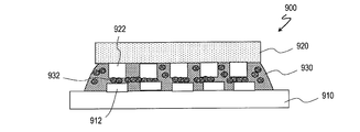
- FIG. 10 shows a conventional chip mounting structure 900 in which the driving IC chip 920 is mounted face-down on the periphery of the liquid crystal panel.
- the driving IC chip 920 is connected to the TFT substrate 910 of the liquid crystal panel using an ACF 930. More specifically, the bump electrode 922 provided on the IC chip 920 and the connection terminal (pad) 912 provided on the TFT substrate 910 are electrically connected by the conductive particles 932 included in the ACF 930 interposed therebetween. Connected. Further, the IC chip 920 is fixed on the TFT substrate 910 by curing the resin material of the ACF 930.
- connection between electronic components such as an IC chip and a wiring board such as a TFT substrate have been proposed.
- an elastic body for example, a resin material.
- Patent Document 1 discloses a structure in which an electronic component mounting substrate is provided with a recess, and the electronic component is accommodated in the recess so that a conductive elastic body is interposed on a side surface of the recess.
- this electronic component mounting structure since the electronic component is pressed against the side surface of the concave portion by the elastic body, the connection electrode on the side surface of the concave portion and the electrode on the side surface of the electronic component are more reliably connected.
- Patent Document 2 discloses a configuration in which pads are arranged on the chip mounting substrate side via a convex elastic body. In this way, high bondability can be obtained regardless of the rigidity of the substrate during chip mounting.
- Patent Document 3 shows a form in which a resin layer is provided on a mounting substrate, and an IC chip bump electrode is embedded in the electrode formed on the resin layer and connected to the substrate. .
- the number of connection terminals of a display panel and the number of bump electrodes of a driving IC chip increase as the number of pixels increases due to higher definition.
- Patent Document 4 describes a technique for dealing with a case where a gap of a bump electrode of a driving IC chip is narrowed.
- This document discloses a bump electrode structure in which only a part of a resin bump formed on a semiconductor device (IC chip) is covered with a conductive film.
- the bump electrode is hemispherical and elastic, and the bump is elastically deformed to obtain contact with the connection terminal on the wiring board. Since the conductive film covers only a part of the bump, good electrical connection is realized while reducing the occurrence of short circuit between adjacent electrodes.
- an anisotropic conductive layer When an anisotropic conductive layer is used as an adhesive when the gap between the bump electrodes is narrow, the diameter of the conductive particles contained in the anisotropic conductive layer (for example, about 3 ⁇ m) is the gap between the electrodes. On the other hand, since it becomes a size which cannot be disregarded, there exists a possibility that an adjacent electrode may short-circuit with electroconductive particle. In order to solve such a problem, an anisotropic conductive layer containing conductive particles of a smaller size, or a resin such as NCF (Non Conductive Film) or NCP (Non Conductive Resin Paste) containing no conductive particles. It is conceivable to use layers. However, when such an adhesive is used, the effect of improving the connectivity utilizing the elastic deformation of the conductive particles contained in the conventional anisotropic conductive layer cannot be expected.
- NCF Non Conductive Film
- NCP Non Conductive Resin Paste
- Patent Document 5 discloses a connection terminal having a configuration in which a conductive layer is arranged so as to cover a convex portion made of a resin material provided on a substrate as a configuration that can cope with connection of a narrow gap terminal. Yes.
- the driving IC chip is mounted using an adhesive (NCF or the like) that does not contain conductive particles. Since the electrodes of the driving IC chip are connected to the connecting terminals having elasticity protruding from the substrate surface, the connection reliability is ensured even when the substrate is warped.
- an adhesive layer that does not include conductive particles a short circuit between terminals in the adhesive layer is prevented.
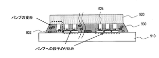
- FIG. 11 shows a configuration in a case where bare chip mounting is performed using an ACF in a narrow gap.
- the width of the bump electrodes 924 is also reduced in order to ensure insulation between adjacent electrodes.
- the bump electrode 924 has a narrower shape than the conventional one, deformation easily occurs. Therefore, when the IC chip 920 is crimped to the connection terminal 912 of the substrate 910, the bump electrode 924 is deformed, resulting in a problem that connection reliability is lowered.
- the bottom area of the bump electrode 924 is reduced, it is considered that pressure is not easily dispersed when the IC chip 920 is pressed against the substrate 910, and a strong force is likely to act on each bump electrode. For this reason, when the pressure bonding is performed, a phenomenon may occur in which the conductive particles dispersed in the ACF 930 are not appropriately elastically deformed and are embedded in the bump electrodes. In this way, in the COG connection with a narrower pitch, the reliability of electrical connection between the IC chip and the terminal on the wiring board is lowered, and the driving stability of the display device or the like is impaired.
- the aspect ratio of the driving IC chip is increased, and a vertically long IC chip has been used.
- a vertically long IC chip the entire IC chip is fixed on the substrate with uniform pressure when mounted on the substrate due to the influence of warpage (due to thermal stress) generated between the IC chip and the TFT substrate. Is relatively difficult.
- the bump electrode having a narrow gap is pressed strongly, the connectivity is deteriorated due to deformation or the like.
- the possibility of a short circuit between adjacent terminals is increased. Therefore, there has been a demand for a mounting structure that enables stable connection even with a smaller load and that is less likely to cause deformation of the bump electrode even when pressed.
- the present invention has been made in view of the above problems, and provides a wiring board capable of obtaining stable connectivity even when the pitch of bump electrodes of a semiconductor chip is reduced and the chip mounting area is narrowed.
- the purpose is to do.
- An electronic circuit board includes a board, a wiring board formed on the board, a wiring, a circuit element, and a connection terminal connected to the circuit element via the wiring, and An electronic circuit board comprising a semiconductor chip mounted on the wiring board via a connection terminal, wherein the connection terminal of the wiring board is a pair of convex parts, and a concave part is formed between them.
- a bump electrode is provided, and a connection region between the concave electrode and the bump electrode is formed in a linear shape.
- each of the pair of convex portions extends along a first direction, and the extending direction of the linear connection region is parallel to the first direction.
- the concave electrode and the bump electrode are directly connected at least partially in the connection region.
- the bump electrode has an edge that defines a bottom surface of the bump electrode, and the recess electrode and the edge of the bump electrode are connected in the connection region.
- the electronic circuit board further includes a resin material layer disposed around the concave electrode and the bump electrode, and the resin material layer is made of NCF or NCP.
- the pair of convex portions has elasticity.
- each of the pair of convex portions has a convex curved surface, and the concave portion is formed by at least the convex curved surface.
- connection terminals in a single mounting region of the semiconductor chip, a plurality of the connection terminals are provided along a predetermined direction, and an arrangement pitch of the connection terminals at an end of the mounting region is: Narrower than the arrangement pitch of the connection terminals in the center of the mounting area.
- connection terminals are provided in a predetermined direction in a single mounting region of the semiconductor chip, and the connection terminals provided at end portions of the mounting region have In the pair of protrusions, one protrusion on the end side of the mounting area is larger in size than the other protrusion on the center side of the mounting area.
- the circuit element includes a TFT and a pixel electrode electrically connected to the TFT, and the wiring includes a gate bus line and a source bus line that connect the connection terminal and the TFT. including.
- a display device includes any one of the electronic circuit boards described above and a display medium layer driven by the electronic circuit board.
- the display device further includes another substrate disposed to face the electronic circuit substrate, and a liquid crystal layer as the display medium layer is sandwiched between the electronic circuit substrate and the another substrate. Has been.
- a wiring board is a wiring board comprising a substrate, a wiring formed on the substrate, a circuit element, and a connection terminal connected to the circuit element via the wiring,
- Each of the connection terminals is a pair of convex portions, a pair of convex portions forming a concave portion between them, and a concave electrode provided in the concave portion and covering at least a part of each of the pair of convex portions
- the recess is formed by a pair of slopes formed by the pair of projections, and the bump electrodes of the semiconductor chip are selectively connected to the recess electrodes on the pair of slopes. ing.
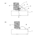
- (A) is a perspective view showing a liquid crystal module of an embodiment of the present invention, and (b) is a cross-sectional view taken along line A-A ′ shown in (a). It is sectional drawing which shows the chip mounting structure concerning embodiment of this invention.
- (A) is a top view which shows the chip mounting structure concerning embodiment of this invention
- (b) is a top view which shows the chip mounting structure of the modification of (a).
- (A) is a top view showing a chip mounting structure corresponding to a staggered arrangement of terminals
- (b) is a top view showing a chip mounting structure of a modification of (a)
- (c) is still another modification. It is a top view which shows an example. It is sectional drawing of the connecting terminal concerning another embodiment of this invention.
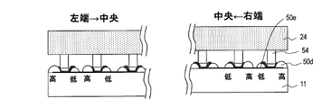
- FIG. 1 It is a top view which shows the chip mounting structure concerning another embodiment of this invention. It is a figure which shows the form of the connection of the bump electrode and connection terminal in a chip mounting structure, (a) shows the case where ACF / ACP is used, (b) shows the case where NCF / NCP is used. It is a figure which shows the modification of embodiment of this invention, and shows the form which changes the arrangement pitch of a connection terminal in IC chip both ends. It is a figure which shows the modification of embodiment of this invention, and shows the form which changes the height of the convex part of a connection terminal in IC chip both ends. It is sectional drawing which shows the conventional COG type face down chip mounting structure. It is sectional drawing which shows the conventional COG type face-down chip mounting structure when the gap between electrodes is narrow.
- a system in which a driving IC chip is COG mounted on a connection terminal on a substrate is widely and generally employed.
- an anisotropic conductive layer such as ACF or ACP is often used.
- ACF anisotropic conductive layer
- leakage short circuit
- Patent Document 5 discloses a mounting structure using NCF.
- the inventor of the present application has also proposed a COG mounting system that can use a non-conductive adhesive (Japanese Patent Application No. 2009-264613).
- a configuration is shown in which, in a chip mounting region, a connection terminal is formed by providing an electrode after providing an insulating layer having a suitable elastic force on a wiring board.
- the driving IC chip is COG-mounted on the wiring board using a non-conductive adhesive or an adhesive containing fine conductive particles of 1 ⁇ m or less, and the bump electrode and the connection terminal are Connected directly.
- the anisotropic conductive layer When the anisotropic conductive layer is not used, it is important that the bump electrode and the connection terminal are in direct contact with stability. This is because if the resin material is interposed between them, sufficient reliability of conduction cannot be obtained. Therefore, in order to obtain a more reliable contact, it is necessary to press the IC chip relatively strongly against the connection terminal to discharge the resin from the contact area.
- the present inventor has a structure capable of COG mounting at a lower pressure corresponding to a narrow pitch, ACF including conductive particles smaller than conventional, NCF (non-conductive particle film), NCP (non-conductive particle paste), etc. Research has been conducted on a configuration that enables stable electrical connection while suppressing short circuit between terminals. As a result, a chip mounting structure that selectively obtains electrical connection with the edge portion of the bump electrode of the driving IC in the concave portion formed between the pair of convex portions formed on the wiring board is obtained. Thus, it has been found that COG mounting can be suitably performed even in the case of a narrow pitch.
- the liquid crystal module 100 includes a display panel 10, a driving IC chip (semiconductor chip) 24 that is COG mounted on the display panel 10, and an FPC (flexible external wiring board) 26 that is connected to the display panel 10. .
- a liquid crystal display device can be manufactured by appropriately combining a known backlight unit (not shown) or the like with the liquid crystal module 100. That is, the liquid crystal display device according to the present embodiment has the same configuration as the conventional liquid crystal display device except that the liquid crystal module 100 is used.
- FIG. 1A shows a form in which only one IC chip 24 is mounted on one side of the display panel 10, but a plurality of IC chips 24 are provided on each of a plurality of sides of the display panel 10. It goes without saying that may be implemented.
- the display panel 10 includes a pair of substrates 11 and 12 and a liquid crystal layer 13 provided between the substrate 11 and the substrate 12.
- the liquid crystal layer 13 is sealed and held between the substrate 11 and the substrate 12 by the seal portion 14.
- An electrode (and wiring), an alignment film, and the like are provided on the surface of the substrate 11 on the liquid crystal layer 13 side as necessary, and a color filter, an electrode (and wiring) and an alignment are provided on the surface of the substrate 12 on the liquid crystal layer 13 side.
- a membrane is provided as needed.
- a switching element (typically TFT) is further provided on the surface of the substrate 11 on the liquid crystal layer 13 side.
- TFT switching element
- substrate 12 are typically formed using a glass substrate.
- the glass substrate and the structure provided on the liquid crystal layer 13 side are referred to as the substrate 11 and the substrate 12.
- the substrate on which the driving IC chip 24 is mounted is called a wiring substrate 11 (typically a TFT substrate), and the other is called a counter substrate 12.
- a TFT, a pixel electrode, or the like provided on the wiring board 11 may be referred to as a circuit element.
- FIG. 1B shows a cross section along the liquid crystal module A-A ′ line shown in FIG.
- the driving IC chip 24 is mounted on the terminal region 11 a of the wiring substrate 11 using an anisotropic conductive film (ACF) 31.
- ACF anisotropic conductive film
- the FPC 26 is connected to the terminal region 11 a of the wiring board 11 using, for example, ACF 32.
- the output terminal of the FPC 26 is connected to the wiring on the wiring board 11 and supplies various signal voltages and power supply voltages to the IC chip 24.
- the bump electrode of the IC chip 24 is connected to the connection terminal of the wiring substrate 11, and the operation of the display panel 10 is controlled by the IC chip 24 through the wiring.
- the liquid crystal module 100 has polarizing plates 17 and 18 on both sides of the display area of the display panel 10. Further, a protective layer 27 made of a resin or the like is provided in the terminal region 11a so as to cover the driving IC chip 24.
- FIG. 2 shows a mounting structure of the driving IC chip 24 on the wiring board 11 in the terminal region 11a, and shows a cross section of the mounting structure along a direction parallel to one side of the IC chip 24.
- the liquid crystal module 100 employs a COG method in which a driving IC chip 24 (driving element, semiconductor chip) is bare-chip mounted on the wiring substrate 11 of the display panel 10. As can be seen from the figure, the driving IC chip 24 is connected and fixed to the wiring board 11 via the ACF 31.
- a narrow gap bump electrode 54 is formed on the driving IC chip 24.
- the bump electrode 54 is face-down bonded to a connection terminal 51 formed on the wiring board 11.
- the bump electrode 54 is formed of a metal having a high conductivity such as Au, and can have various forms.
- the bump electrode 54 has a substantially rectangular parallelepiped shape, and the bottom surface has a rectangular shape. Yes.
- connection terminals 51 formed in the terminal area 11 a of the wiring board 11 has a pair of protrusions (projections) 50 protruding from the main surface of the wiring board 11.
- a concave portion 60 is formed between the convex portions 50 a and 50 b, and an electrode (concave electrode) 52 is provided so as to cover the concave portion 60.
- Each of the pair of convex portions 50 has a semi-cylindrical shape, for example (see FIG. 3A, etc.).
- the recess 60 is a space at least partially surrounded by a curved surface defined as a side surface of a cylinder.
- the concave portion 60 is not limited to this, and may be formed by a curved surface having another shape (preferably a convex curved surface).
- the convex portions 50a and 50b are formed of an elastic body, and are formed using, for example, polyimide, acrylic resin, photosensitive resin, or the like.
- the protrusions 50a and 50b formed using such a material are formed in the same step in a panel manufacturing process including a step of providing the above material with a predetermined thickness over the entire display region immediately below the pixel electrode, for example. Can be done.
- the resin material layer provided immediately below the pixel electrode is used to reduce parasitic capacitance formed between the pixel electrode and the source or gate bus line.
- the recessed electrode 52 can be formed at the same time in the step of forming the pixel electrode. In this way, it is also possible to produce the connection terminal 51 composed of the convex portion 50 and the concave electrode 52 without adding another process to the conventional liquid crystal panel manufacturing process. Of course, the connection terminal 51 may be formed separately.
- the concave electrode 52 can be formed at the same time as the pixel electrode as described above. However, when the pixel electrode is formed of a transparent conductive film such as ITO, the concave electrode 52 is made of another metal film having high elasticity (for example, you may make it form from an aluminum film. By doing in this way, it is prevented that the elastic deformation of the convex part 50 is inhibited by the concave electrode 52. Further, when the recessed electrode 52 is formed of a material rich in elasticity and toughness, there is an advantage that cracks are hardly generated in the recessed electrode 52 when the protruding portion 50 is elastically deformed during chip mounting. In the reflective display device or the transflective display device, when the pixel electrode is formed of aluminum or the like, it is preferable that the concave electrode 52 is also formed of the same material in the step of forming the pixel electrode.
- FIG. 3A is a top view showing the arrangement of the connection terminals 51 and the bump electrodes 54.
- the convex portions 50a and 50b forming the concave portion 60 typically extend along the short side direction of the IC chip 24 to be mounted.
- the connection terminal 51 and the bump electrode 54 are connected at the edge portion of the bottom surface of the bump electrode 54.
- the connection region between the connection terminal 51 and the bump electrode 54 is formed substantially parallel to the extending direction of the convex portion 50.
- the arrangement of the convex portions 50a and 50b and the arrangement of the concave electrode 52 covering the concave portion 60 are not limited to the illustrated form.
- a common convex portion 50c can be used for two adjacent bump electrodes 54.
- the pair of convex portions 50 provided corresponding to one bump electrode 54 are not necessarily separated from each other, and may be integrally formed as long as the concave portion 60 is formed.
- connection terminals 51 may be arranged in a staggered manner so as to be compatible with the IC chip 24 in which the bump electrodes 54 are arranged in a staggered manner. With such an arrangement, wiring between the signal lines and scanning lines provided on the display panel 10 and the connection terminals 51 becomes easier.
- the connection terminals 51 with a narrow gap if the connection terminals 51 are arranged in a staggered manner, it is not necessary to wire the terminals so as to pass between adjacent connection terminals 51 even when the terminals are arranged in a plurality of rows.
- the connection terminal 51 can be easily wired. In this way, thicker wiring can be provided in a straight line.
- FIG. 1 In FIG.
- a common convex portion 50c is provided as one of the pair of convex portions 50a and 50b for two bump electrodes 54 adjacent in the oblique direction.
- FIG.4 (b) you may provide a pair of convex part 50a, 50b separately to each adjacent bump electrode 54, respectively.
- FIG. 4C common protrusions 50a and 50b may be provided on the bump electrodes 54 adjacent in the lateral direction.
- the wiring 52l extending from the liquid crystal panel and the concave electrode 52 formed on the pair of convex portions 50a and 50b (convex portion 50) are typically formed in separate steps. Is done.
- the wiring 52l is formed in the same layer as the source or gate bus line, and then the convex portion 50 is formed, and then the concave electrode 52 is provided so as to be electrically connected to the wiring 52l.
- the wiring 52l since the wiring 52l is provided in the lower layer of the convex portion 50, the wiring 52l can be formed in a desired pattern without depending on the shape of the convex portion 50. For example, in order to obtain a structure as shown in FIG.
- the convex portion 50 is formed on the wiring provided in a predetermined pattern, and then the convex portion 50 is partially covered and is appropriately connected to the wiring.
- the concave electrode 52 may be formed in a desired pattern so that an electrical connection can be obtained.
- FIG. 5 shows a form in which the electrical connection between the wiring 52l and the recessed electrode 52 is formed between the pair of convex parts 50a and 50b. It may be.
- a resin layer including the convex portion 50 is formed over the wiring, and the wiring 52l and the concave electrode 52 are electrically connected through a contact hole provided at an arbitrary position of the resin layer. Also good.
- the convex portion 50x may have a rectangular annular shape composed of four linear portions facing the edges of the four sides of the bottom surface portion of the bump electrode.
- two opposing sides of the part forming the convex part may be expressed as a pair of convex parts.
- the ACF 31 is applied on the wiring substrate 11 on which the connection terminals 51 are formed in the terminal region 11a, and then the alignment between the wiring substrate 11 and the driving IC chip 24 is performed. Thereafter, heat pressure bonding is performed from the driving IC chip 24 side using a pressure bonding tool or the like.
- the pressure bonding conditions are, for example, a temperature of 160 ° C. to 210 ° C., a pressing force of 40 MpPa to 100 MPa, and a pressing time of 5 seconds to 20 seconds.
- connection terminal 51 and the bump electrode 54 are elastically deformed (flattened) by being thermocompression-bonded, and the deformed state is maintained by curing the surrounding insulating adhesive. It will be fixed as it is. As a result, electrical connection between the connection terminal 51 and the bump electrode 54 is ensured and electrical connection is realized.
- the driving IC chip 24 is fixed onto the wiring substrate 11 while the electrical connection between the IC chip 24 and the wiring substrate 11 is formed by thermocompression bonding of the ACF 31 in this manner.
- the ACF 31 used in the present embodiment can be obtained by mixing conductive particles in an insulating adhesive.
- the particle diameter of the conductive particles is, for example, 2 to 3 ⁇ m, and the packing density of the conductive particles is set to, for example, 55000 to 60000 particles / mm 2 .
- the conductive particles those formed by performing gold plating after nickel plating on a plastic sphere can be used.
- the insulating adhesive contains, for example, an epoxy resin having a weight average molecular weight in the range of 10,000 to 100,000, an epoxy resin having a weight average molecular weight of 1000 or less, and a curing agent.
- ACF31 made of such a material has a Young's modulus after curing of 1.4 GPa to 2.0 GPa and a glass transition temperature after curing of 110 ° C. to 135 ° C.
- connection region between the bump electrode 54 and the connection terminal 51 (recessed electrode 52) is formed in a linear shape, and these electrical connections can be suitably obtained with a lower load. Since the bonding can be performed, it is not always necessary to use the ACF 31 as described above. That is, it is possible to use a resin layer (adhesive layer) containing conductive particles that are smaller and less elastic, or a resin layer that does not contain conductive particles as described later.
- the connection terminal 51 when the electrical connection between the bump electrode 54 and the connection terminal 51 is formed through the anisotropic conductive layer made of ACF 31, the side surface and edge portion of the bump electrode 54 and the convex portion are formed.
- the side surface of the recessed electrode 52 (not shown in FIG. 7A) on the 50 is connected.
- ACP is used instead of ACF 31.
- the connection can be realized by utilizing the elastic deformation in the oblique direction of the conductive particles 33 sandwiched between the bump electrode 54 and the recessed electrode 52.
- a force acts on the conductive particles 33 interposed between the bump electrode 54 and the recessed electrode 52.
- the bump electrode 54 and the recessed electrode 52 are selectively connected at the edge portion or side surface portion of the bump electrode 54 (that is, the bump electrode 54 is typically formed only at the edge portion or side surface portion. It is because it is comprised so that it may contact 52.
- the connection region between the concave electrode 52 and the bump electrode 54 is formed linearly along the direction in which the convex portion 50 extends. In this case, it is possible to obtain an electrical connection by elastically deforming the conductive particles 33 of the ACF 31 with a smaller load than in the conventional configuration in which the connection is made over the entire bottom surface of the bump electrode.
- the contraction force C generated by the resin material of the ACF 31 after the cooling is used as a force vector acting in the connection direction between the bump electrode 54 and the connection terminal 51 (see FIG. 2). can do.
- the thickness of the resin layer of the ACF 31 is larger than when the bottom surface of the bump electrode and the planar connection terminal are joined. Is getting bigger.
- the resin layer of ACF31 thicker than the conventional structure, it is possible to obtain a larger cohesive force B than that in the past when the resin material functioning as an adhesive is cured. Thereby, the connection by a low load is realizable.
- the cohesive force refers to an attractive force that acts between molecules of the adhesive or pressure-sensitive adhesive.
- connection region is formed in a linear shape, and the resin material is more easily discharged at the time of pressure bonding than in the case of surface contact, the conductive material is cured by first curing the resin material. It is suppressed that the load to 33 is inhibited, and thereby, the insufficiency of pushing of the conductive particles 33 can be improved.
- the bump electrode 54 is connected to the connection terminal 51 on the side surface (slope) of the convex portion 50. For this reason, it is preferable that the recessed electrode 52 is provided at least on the side surface of the protruding portion 50 (or the recessed portion 60). Further, unlike the conventional configuration, the deformation of the conductive particles 33 located below the bump electrode 54 may be insufficient.
- the connection at the bottom surface of the bump electrode 54 can be considered auxiliary.
- the bump electrode 54 having a narrow width is supported in the concave portion 60 formed by the pair of convex portions 50 so as to be sandwiched from the left and right, and the convex portion 50 (or the concave portion 60) is supported.
- An electrical connection is formed on the side surface or the like.
- the connection region (edge of the bump electrode 54) where electrical connection can be obtained is preferably formed in a linear shape along the direction in which the convex portion 50 extends. In this configuration, it is not necessary to strongly press the bump electrode 54 against the wiring substrate 11 during pressure bonding, and the load acting on the bump electrode 54 and the substrate 11 can be reduced. Therefore, it is possible to improve the connection reliability while preventing the bump electrode 54 from being deformed.
- the reliability of the connection is ensured even when the bump electrode has a narrow pitch. be able to.
- This configuration is particularly effective when the arrangement pitch of the bump electrodes or connection terminals is 20 ⁇ m or less, and more effective when it is 13 ⁇ m or less.
- connection material not only ACF and ACP but also NCF or NCP can be used as the connection material.
- a non-conductive adhesive such as NCF or NCP
- it is preferable that the convex portion 50 is formed of a material having a predetermined elastic force.
- FIG. 7B shows a connection form when a non-conductive adhesive such as NCF or NCP is used.
- NCF non-conductive adhesive
- NCP non-conductive adhesive
- the edge portion and side surface portion of the bump electrode 54 are formed on the convex portion 50 while elastically deforming the convex portion 50 having elasticity. It directly adheres to the recessed electrode 52 (not shown in FIG. 7B). Thereby, the bump electrode 54 and the recessed electrode 52 are electrically connected.
- an anisotropic conductive layer including conductive particles having a relatively large diameter as in the past as an adhesive layer it is possible to use an adhesive layer including the same, and even when the terminals are provided at a narrow pitch, occurrence of leakage between terminals can be suppressed.
- the concave electrode 52 is provided on the wiring board as described above.
- a very thin high-resistance film such as an oxide film or a hydroxide film may be formed on the surface thereof.
- the conductive particles can break through the high-resistance film. The electrical connectivity can be improved.
- the convex portion 50 is formed of an elastic material, the elastically deformed convex portion 50 is restored in the direction of the bump electrode 54 even when the adhesive is expanded by moisture absorption or heat after chip mounting. Therefore, the stability of the electrical connection is maintained. Further, even when there is a difference in the height of the bump electrode 54, it is possible to absorb this difference by elastic deformation of the convex portion 50 and obtain a suitable electrical connection at each terminal.
- connection terminal 51 does not have elasticity
- the connection reliability can be maintained by the elastic characteristics of the conductive particles dispersed in the ACF or ACP. .
- the convex part 50 may be formed with the material lacking in elasticity.
- the arrangement pitch P1 of the connection terminals 51 is made smaller at the end of the region where the plurality of connection terminals 51 corresponding to one mounted IC chip 24 is provided than at the center. ing.
- the pitch P0 of the bump electrodes 54 of the IC chip 24 is constant.
- the arrangement pitch P1 of the connection terminals 51 is reduced only at the end portion, a force for moving the IC chip 24 in the horizontal direction to the center portion is applied during crimping. Since this force is applied from both sides of the IC chip 24 and balanced, the IC chip 24 and the connection terminal 51 are easily aligned properly.
- Such alignment of the IC chip 24 and the connection terminal 51 can also be realized by changing the size (height) of the convex portion 50 within the chip mounting area as shown in FIG. If the convex portion 50d on the outer side (end portion) is made higher and the convex portion 50e in the center direction is made lower, when the IC chip 24 is pressed against the wiring substrate 11, the force from both ends of the IC chip 24 toward the center is increased. work.
- the wiring board preferably has a concave connection terminal having a predetermined elasticity on the surface, so that the edge of the bump electrode and the side surface of the depression by the elastic body can be joined.
- a concave connection terminal having a predetermined elasticity on the surface, so that the edge of the bump electrode and the side surface of the depression by the elastic body can be joined.
- connection terminal polyimide, acrylic resin, photosensitive resin or the like can be used.
- a resin material containing Ni particles or metal nanoparticles for example, a diameter of about 1 ⁇ m or less is used as an adhesive material interposed between the bump electrode and the connection terminal. it can.
- the convex portion constituting the connection terminal on the wiring board may not have elasticity. Further, as described above, it is possible to provide a terminal group including a plurality of staggered arrays as well as a single-row array.
- a general manufacturing process of a reflective or transflective liquid crystal display device can be used. However, an elastic resin layer forming process for forming the convex portion is provided as necessary.
- the mounting structure of the driving IC chip in the liquid crystal display device has been described.
- the present invention is not limited to this embodiment, and a semiconductor chip (for example, an IC chip or an LED chip) is mounted face-down on a circuit board.
- a semiconductor chip for example, an IC chip or an LED chip
- connection reliability can be improved while suppressing a short circuit between terminals.
- An electronic circuit board obtained by mounting a semiconductor chip on the wiring board of the present invention is suitably used in various electronic devices such as a liquid crystal display device, an organic EL display device or an image sensor.
- connection terminals formed on the wiring board can be arbitrary so as to correspond to the arrangement of the terminals (electrodes) of the chip to be mounted.
- the present invention can be applied not only to a rectangular driver IC chip but also to a chip in which electrodes are provided in an array in a square chip, for example.
- the embodiment of the present invention is preferably used for COG mounting a driving IC chip in a liquid crystal module used in a display device.
- Embodiments of the present invention are not limited to liquid crystal modules, and can also be applied to organic EL modules and the like.
- the display device according to the embodiment of the present invention may be a plasma display panel, a field emission display, or the like.
Landscapes
- Physics & Mathematics (AREA)
- Nonlinear Science (AREA)
- Engineering & Computer Science (AREA)
- Microelectronics & Electronic Packaging (AREA)
- Mathematical Physics (AREA)
- Chemical & Material Sciences (AREA)
- Crystallography & Structural Chemistry (AREA)
- General Physics & Mathematics (AREA)
- Optics & Photonics (AREA)
- Liquid Crystal (AREA)
- Wire Bonding (AREA)
Abstract
配線基板(11)は、基板と、基板上に形成された、複数の配線、複数の回路素子、および複数の配線を介して接続された複数の接続端子(51)とを備えている。複数の接続端子(51)のそれぞれは、一対の凸部(50)であって、それらの間に凹部(60)を形成する一対の凸部(50)と、凹部(60)において設けられ、一対の凸部(50)のそれぞれの少なくとも一部を覆う凹部電極(52)とを有する。
Description
本発明は、電子回路基板、表示装置および配線基板に関し、特に、半導体チップが配線基板にフェイスダウン実装された構造に関する。
近年、液晶表示装置や有機EL表示装置などの薄型表示装置が、例えばテレビジョンまたは携帯電話やスマートフォン等の表示装置として広く用いられている。これらの薄型表示装置には、表示パネルに駆動信号を供給するための駆動回路(典型的には駆動用ICチップ)が設けられている。表示パネルは少なくとも1枚の透明基板を有しており、駆動回路が形成されたICチップが、この透明基板上に実装される構成を採るものが多い。
例えば、TFT型液晶表示装置は、ガラス基板上に画素毎に設けられた画素電極と、画素電極毎に少なくとも1つ設けられたTFTと、画素電極にTFTを介して接続される信号線(ソースバスライン)と、TFTのスイッチングを制御するためにTFTに接続された走査線(ゲートバスライン)とを有する。信号線や走査線に所定の信号(データ信号や走査信号)を供給する駆動用ICチップは、同じガラス基板(TFT基板)上に実装される。
駆動用ICチップの実装構造としては、近年では、低コスト、高信頼性、薄型化等の観点から、液晶パネルのガラス基板に駆動用ICチップをベアチップ実装するCOG(Chip On Glass)方式が用いられている。また、他方式としては、フィルム上に駆動用ICチップを実装するCOF方式も知られている。
COG方式の一つとして、駆動用ICチップの回路形成面に突起状のバンプ電極を形成し、このバンプ電極を液晶パネルのガラス基板に形成されたパッド(走査線や信号線の接続端子電極、ボンディングパッドともいう。)に接続する、いわゆるフェイスダウン実装構造が知られている。この実装構造において、例えば、バンプ電極はAuなどの金属により形成され、例えば異方性導電層を介してパッドと接続される。
異方性導電層は、その厚さ方向に導電性を有する一方で、層面内方向には導電性を有しないので、導電層をパターニングする必要が無く、異方性導電層を介して互いに対向するバンプ電極とパッドとを電気的に接続することができる。また、隣接する電極間には樹脂材料(接着材)が充填されるので絶縁信頼性にも優れる。異方性導電層は、異方性導電フィルム(ACF)や異方性導電性ペースト(ACP)などを用いて形成される。
図10は、液晶パネル周縁部において駆動用ICチップ920がフェイスダウン実装されている従来のチップ実装構造900を示す。図示するように、駆動用ICチップ920は、液晶パネルのTFT基板910上にACF930を用いて接続されている。より具体的には、ICチップ920に設けられたバンプ電極922と、TFT基板910に設けられた接続端子(パッド)912とが、これらの間に介在するACF930に含まれる導電性粒子932によって電気的に接続されている。また、ACF930の樹脂材料が硬化することによって、ICチップ920がTFT基板910上に固定されている。
ICチップなどの電子部品と、TFT基板などの配線基板との接続形態としては様々な形態が提案されており、例えば、弾性体(例えば樹脂材料)を用いて接続の確実性を向上させる技術が知られている。
特許文献1には、電子部品実装基板に凹部を設け、この凹部の側面において導電性の弾性体が介在するように電子部品を凹部に収納する構造が示されている。この電子部品実装構造においては、弾性体によって電子部品が凹部側面に押圧されるので、凹部側面の接続電極と電子部品側面の電極とがより確実に接続される。
また、特許文献2には、チップ実装基板側に凸状の弾性体を介してパッドを配置する構成が開示されている。このようにすれば、チップ実装時に基板の剛性によらず高い接合性が得られる。また、特許文献3には、実装基板上に樹脂層を設け、この樹脂層上に形成された電極に対してICチップのバンプ電極がめり込んだ状態で基板に接続される形態が示されている。
液晶表示装置などの表示装置では、高精細化による画素数の増加にともない、表示パネルの接続端子数および駆動用ICチップのバンプ電極数が増加している。一方で、製造コストや製品サイズの観点からICチップのサイズをなるべく小さくすることが望まれている。特に狭額縁化が進む表示装置においては、表示パネル周辺の額縁領域に大型のICチップを搭載することは困難である。
これらの結果、多数のバンプ電極を有する小型のICチップを配線基板上に実装する必要が生じている。このようなICチップを用いる場合、ICチップのバンプ電極の配列ピッチ(または配線基板上のパッドの配列ピッチ)は非常に小さく、隣接するバンプ電極間のギャップが狭くなる。したがって、狭ギャップのバンプ電極同士の絶縁性を確保しながら、パッドとの安定した接続を得ることが必要である。
特許文献4には、駆動用ICチップのバンプ電極のギャップが狭くなった場合に対応するための技術が記載されている。この文献には、半導体装置(ICチップ)に形成された樹脂製のバンプの一部分だけを導電膜で覆う形状のバンプ電極構造が開示されている。このバンプ電極は半球状で弾性を有しており、バンプを弾性変形させるようにして配線基板上の接続端子との接触を得ている。バンプの一部のみを導電膜が覆うので、隣接する電極間での短絡の発生を低減しつつ良好な電気的接続が実現される。
また、バンプ電極間のギャップが狭いときに接着材として異方性導電層を用いる場合には、異方性導電層に含まれる導電性粒子の直径(例えば、約3μm)が、電極間ギャップに対して無視できない大きさになるため、隣接する電極が導電性粒子によって短絡する恐れがある。このような問題を解決するためには、より小さいサイズの導電性粒子を含む異方性導電層や、導電性粒子を含まないNCF(Non Conductive Film)やNCP(Non Conductive Resin Paste)などの樹脂層を用いることが考えられる。しかし、このような接着材を用いる場合には、従来の異方性導電層に含まれる導電性粒子の弾性変形を利用した接続性向上の効果は期待できない。
特許文献5には、狭ギャップの端子の接続に対応し得る構成として、基板上に設けられた樹脂材料からなる凸部を覆うように導電層が配置された構成を有する接続端子が開示されている。この構成において、導電性粒子を含まない接着材(NCFなど)を用いて駆動用ICチップを実装することが記載されている。基板面から突出した状態の弾性を有する接続端子に対して、駆動用ICチップの電極が接続されるため、基板の反りなどが生じたときにも接続の信頼性が確保される。また、導電性粒子を含まない接着層を用いることによって、接着層において端子間の短絡が発生することが防止される。
しかしながら、表示装置の高精細化や狭額縁化が進むにつれ、電極のギャップは更に狭くなることが予想される。この場合、上記に説明した従来のフェイスダウン実装構造では、安定した接続を得ることが困難になると考えられる。以下、この問題に対する本発明者の考察を説明する。
図11は、狭ギャップ時においてACFを用いてベアチップ実装を行う場合の構成を示す。図11に示すように、バンプ電極924の配列ピッチを小さくする場合には、隣接する電極間の絶縁性を確保するためにバンプ電極924の幅も小さくされる。このようにバンプ電極924が従来より細幅形状となると変形が生じやすくなる。したがって、基板910の接続端子912にICチップ920を圧着するときにバンプ電極924が変形することで接続の信頼性が低下するという問題が生じる。
また、バンプ電極924の底部面積が小さくなると、ICチップ920を基板910に押しつける際に圧力が分散しにくく、個々のバンプ電極により強い力が作用しやすくなると考えられる。このため、圧着したときに、ACF930に分散されている導電性粒子が適切に弾性変形せずにバンプ電極にめり込むという現象が生じ得る。このようにして、より狭ピッチ化したCOG接続において、ICチップと配線基板上端子との電気的接続の確実性が低下し、表示装置などの駆動の安定性が損われる。
また、表示装置の狭額縁化によって、駆動用ICチップのアスペクト比が大きくなり、縦長形状のICチップが用いられてきている。縦長形状のICチップを用いる場合、ICチップとTFT基板との間に発生する反り(熱応力に起因)などの影響で、基板への実装時にICチップ全体を基板上に均一な圧力で固着することが比較的困難である。この場合、ICチップのバンプ電極全体で十分な接続性を得るためには、より強く押圧することが考えられる。しかし、狭ギャップのバンプ電極を強く押圧すると、変形が生じることなどによって接続性が低下してしまう。また、隣接する端子間でショートが生じる可能性も高まる。したがって、より小さい荷重でも安定した接続が可能で、押圧時にもバンプ電極の変形が生じにくい実装構造が求められていた。
本発明は上記課題を鑑みてなされたものであり、半導体チップのバンプ電極のピッチが小さくなり、チップ実装領域の狭小化が進んだ場合にも安定した接続性を得ることができる配線基板を提供することをその目的とする。また、この配線基板に半導体チップが接続された電子回路基板を提供することを目的とする。さらに、この電子回路基板を備える表示装置を提供することを目的とする。
本発明の実施形態による電子回路基板は、基板と、前記基板上に形成された、配線、回路素子、および前記回路素子に前記配線を介して接続された接続端子とを備える配線基板と、前記接続端子を介して前記配線基板上に実装された半導体チップとを備える電子回路基板であって、前記配線基板の前記接続端子は、一対の凸部であって、それらの間に凹部を形成する一対の凸部と、前記凹部において設けられ、前記一対の凸部のそれぞれの少なくとも一部を覆う凹部電極とを有しており、前記半導体チップは、前記接続端子の前記凹部電極と接続されるバンプ電極を有しており、前記凹部電極と前記バンプ電極との接続領域が線状に形成されている。
ある実施形態において、前記一対の凸部のそれぞれは第1の方向に沿って延びており、前記線状の接続領域の延びる方向は前記第1の方向と平行である。
ある実施形態において、前記凹部電極と、前記バンプ電極とは、前記接続領域において、少なくとも部分的に直接接続されている。
ある実施形態において、前記バンプ電極は、前記バンプ電極の底面を規定するエッジを有しており、前記接続領域において前記凹部電極と前記バンプ電極の前記エッジとが接続される。
ある実施形態において、前記電子回路基板は、前記凹部電極と前記バンプ電極との周辺に配置される樹脂材料層をさらに含み、前記樹脂材料層は、NCFまたはNCPから形成されている。
ある実施形態において、前記一対の凸部は弾性を有する。
ある実施形態において、前記一対の凸部のそれぞれは凸状曲面を表面に有し、少なくとも前記凸状曲面によって前記凹部が形成されている。
ある実施形態において、単一の前記半導体チップの実装領域において、複数の前記接続端子が所定方向に沿って並ぶように設けられており、前記実装領域の端部における前記接続端子の配列ピッチは、前記実装領域の中央部における前記接続端子の配列ピッチよりも狭い。
ある実施形態において、単一の前記半導体チップの実装領域において、複数の前記接続端子が所定方向に沿って並ぶように設けられており、前記実装領域の端部に設けられた前記接続端子が有する一対の凸部において、前記実装領域の端部側の一方の凸部が、前記実装領域の中央部側の他方の凸部よりもサイズが大きい。
ある実施形態において、前記回路素子は、TFTと、前記TFTに電気的に接続された画素電極とを有し、前記配線は、前記接続端子と前記TFTとを接続するゲートバスラインおよびソースバスラインを含む。
本発明の実施形態による表示装置は、上記いずれかの電子回路基板と、前記電子回路基板によって駆動される表示媒体層とを備える。
ある実施形態において、前記表示装置は、前記電子回路基板と対向して配置される別基板をさらに有し、前記電子回路基板と前記別基板との間に前記表示媒体層としての液晶層が挟持されている。
本発明の実施形態による配線基板は、基板と、前記基板上に形成された、配線、回路素子、および前記回路素子に前記配線を介して接続された接続端子とを備える配線基板であって、前記接続端子のそれぞれは、一対の凸部であって、それらの間に凹部を形成する一対の凸部と、前記凹部において設けられ、前記一対の凸部のそれぞれの少なくとも一部を覆う凹部電極とを有し、前記一対の凸部が形成する一対の斜面によって前記凹部が形成されており、前記一対の斜面において半導体チップのバンプ電極が前記凹部電極と選択的に接続されるように構成されている。
本発明によれば、狭ギャップの端子(電極)が配列されている半導体チップをCOG実装する場合にも、端子間の短絡を防止しながら、安定した電気的接続を得ることができる。
基板上の接続端子に対して駆動用ICチップをCOG実装する方式が広く一般的に採用されている。チップと基板との接続を得る方法としては、ACFまたはACPなどの異方性導電層を用いる場合も多い。しかし、上述のように、端子の狭ピッチ化が進むと、ACFに含まれる導電性粒子のサイズ等によって、隣接端子間でのリーク(ショート)が生じ易くなるという問題が発生する。リークの発生を抑制するためには、導電性粒子の直径を小さくすることも考えられるが、導電性粒子のサイズを小さくすると、粒子の十分な弾性変形を確保することが困難になり、その結果、接続の信頼性が低下する。
このような問題を考慮して、より小さい導電性粒子を含むACFを用いたときにも適切に電気的接続が得られるCOG実装方式、もしくは、ACFを用いずに、例えば、NCFやNCPなどの非導電性接着材を用いてCOG実装を行う方式が検討され、例えば、特許文献5にはNCFを用いた実装構造が開示されている。また、本願発明者によっても、非導電性接着材を使用可能なCOG実装方式が提案されている(特願2009-264613号)。ここでは、チップ実装領域において、好適な弾性力を有する絶縁層を配線基板上に設けた後に電極を設けることで接続端子を形成する構成を示している。このような構成において、駆動用ICチップは、非導電性接着材、あるいは、1μm以下の微細な導電性粒子を含む接着材を用いて配線基板上にCOG実装され、バンプ電極と接続端子とは直接的に接続される。
異方性導電層を用いない場合には、バンプ電極と接続端子とが安定して直接的に接触することが重要である。これらの間に樹脂材料が介在すると、導通の信頼性が十分に得られないからである。したがって、より確実な接触を得るために、接続端子に対してICチップを比較的強く押圧して、接触領域から樹脂を排出する必要がある。
しかしながら、狭ピッチで変形が生じやすいバンプ電極に大きな荷重をかけることは、接続信頼性の低下やリークの発生につながるため好ましくない。本発明者は、狭ピッチに対応し、より低い圧力でCOG実装が可能な構造として、従来より小さい導電性粒子を含むACFや、NCF(無導電粒子フィルム)、NCP(無導電粒子ペースト)などを用いることを可能とし、端子間短絡を抑制しつつ安定した電気的接続を得る構成について鋭意研究を行った。その結果、配線基板上に形成した一対の凸部間に形成された凹部において、典型的には駆動用ICのバンプ電極のエッジ部分と選択的に電気的接続を得るようなチップ実装構造とすることによって、狭ピッチの場合にも好適にCOG実装を実施できることを見出した。
以下、図面を参照しながら本発明の実施形態を説明するが、本発明はこれらの実施形態に限定されるものではない。
図1(a)および(b)は、本発明の実施形態にかかる液晶表示装置に用いられる液晶モジュール100を模式的に示す。液晶モジュール100は、表示パネル10と、表示パネル10にCOG実装された駆動用ICチップ(半導体チップ)24と、表示パネル10に接続されたFPC(フレキシブル外部配線基板)26とを有している。
なお、液晶モジュール100に公知のバックライトユニット(図示せず)などを適切に組み合わせることで液晶表示装置を作製することができる。すなわち、本実施形態にかかる液晶表示装置は、液晶モジュール100を用いること以外は、従来の液晶表示装置と同様の構成を有している。また、図1(a)には、表示パネル10の一辺においてICチップ24が1つだけ実装されている形態が示されているが、表示パネル10の複数の辺のそれぞれにおいて複数のICチップ24が実装される形態であっても良いことは言うまでもない。
表示パネル10は、一対の基板11および12と、基板11と基板12との間に設けられた液晶層13とを有している。液晶層13はシール部14によって基板11と基板12との間に封入保持されている。基板11の液晶層13側表面には、電極(および配線)や配向膜などが必要に応じて設けられており、基板12の液晶層13側表面にはカラーフィルター、電極(および配線)および配向膜が必要に応じて設けられている。
アクティブマトリクス型液晶表示装置においては、さらに、基板11の液晶層13側表面にスイッチング素子(典型的にはTFT)が設けられている。簡単のためにこれらは図示していない。なお、基板11および基板12は、典型的には、ガラス基板を用いて形成される。ここでは、ガラス基板とその液晶層13側の設けられた上記の構成を含めて、基板11および基板12と呼ぶことにする。また、駆動用ICチップ24が実装される基板を配線基板11(典型的にはTFT基板)と呼び、他方を対向基板12と呼ぶ。なお、本明細書において、配線基板11に設けられているTFTや画素電極などを回路素子と称することがある。
図1(b)は、図1(a)に示す液晶モジュールA-A’線に沿った断面を示す。配線基板11の端子領域11aにおいて、表示パネル10から延びる配線や、後述する接続端子51(図2参照)が形成されている。駆動用ICチップ24は、異方性導電フィルム(ACF)31を用いて配線基板11の端子領域11aに実装されている。また、FPC26は、配線基板11の端子領域11aに例えばACF32を用いて接続されている。FPC26の出力端子は配線基板11上の配線に接続されており、ICチップ24に種々の信号電圧および電源電圧などを供給する。また、ICチップ24のバンプ電極は、配線基板11の接続端子に接続されており、配線を介して表示パネル10の動作がICチップ24によって制御される。
また、液晶モジュール100は、表示パネル10の表示領域の両側において偏光板17および18を有している。さらに、端子領域11aにおいて、駆動用ICチップ24を覆うように樹脂などからなる保護層27が設けられている。
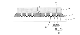
図2は、上述の端子領域11aにおける駆動用ICチップ24の配線基板11への実装構造を示し、ICチップ24の一辺に平行な方向に沿った実装構造の断面を示している。液晶モジュール100では、駆動用ICチップ24(駆動素子、半導体チップ)が表示パネル10の配線基板11にベアチップ実装されるCOG方式が採用されている。図からわかるように駆動用ICチップ24は、ACF31を介して配線基板11に接続および固定されている。
駆動用ICチップ24には、狭ギャップのバンプ電極54が形成されている。このバンプ電極54は、配線基板11上に形成された接続端子51に対してフェイスダウンボンディング接続されている。バンプ電極54は、例えばAuなどの高導電率の金属で形成されており、種々の形態を有し得るが、典型的には、略直方体を為し、その底面は長方形の形状を有している。
配線基板11の端子領域11aに形成された接続端子51のそれぞれは、配線基板11の主面から突出する一対の凸部(突起体)50を有する。それぞれの凸部50a、50bの間には凹部60が形成されており、この凹部60を覆うように電極(凹部電極)52が設けられている。一対の凸部50のそれぞれ50a、50bは、例えば、半円柱状の形状を有する(図3(a)等参照)。凹部60は、円柱の側面として規定される曲面によってその少なくとも一部が囲まれた空間である。ただし、凹部60はこれに限られず、他の形状の曲面(好ましくは凸状曲面)によって形成されていてもよい。
本実施形態では、凸部50a、50bが弾性体から形成されており、例えば、ポリイミド、アクリル樹脂、感光性樹脂等を用いて形成されている。このような材料を用いて形成される凸部50a、50bは、例えば、画素電極の直下において上記の材料を所定の厚さで表示領域全体にわたって設ける工程を含むパネル製造プロセスにおいて、同工程で形成され得る。画素電極直下に設けられる樹脂材料層は、画素電極とソースまたはゲートバスラインなどとの間に形成される寄生容量を低減するために利用される。一方、凹部電極52は、画素電極を形成する工程において同時に形成され得る。このようにして、凸部50と凹部電極52とから構成される接続端子51を、従来の液晶パネル製造工程に対して別の工程を新たに追加することなく作製することも可能である。もちろん、接続端子51を別途形成してもよい。
凹部電極52は、上述のように画素電極と同時に形成することが可能であるが、画素電極がITOなどの透明導電膜から形成される場合、凹部電極52を、弾性に富む他の金属膜(例えば、アルミニウム膜)から形成するようにしてもよい。このようにすることで、凸部50の弾性変形が凹部電極52によって阻害されることが防止される。また、凹部電極52が弾性やじん性に富む材料から形成されている場合には、チップ実装時に凸部50が弾性変形したときに、凹部電極52にクラックが生じにくいという利点も得られる。なお、反射型表示装置または半透過型表示装置において、画素電極をアルミニウムなどから形成するときには、この画素電極を形成する工程において凹部電極52も同材料で形成することが好ましい。
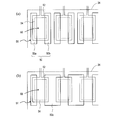
図3(a)は、接続端子51とバンプ電極54との配置を示す上面図である。図示するように、凹部60を形成する凸部50aおよび50bは、典型的には、実装されるICチップ24の短辺方向に沿って延びている。また、接続端子51とバンプ電極54とは、図2などからわかるように、バンプ電極54の底面のエッジ部分において接続している。この接続形態において、接続端子51とバンプ電極54との接続領域は、凸部50の延びる方向に沿ってこれと略平行に形成されている。ただし、凸部50aおよび50bの配置や、凹部60を覆う凹部電極52の配置は図示する形態に限られるものではない。
例えば、図3(b)に示すように、隣接する2つのバンプ電極54に対して共通の凸部50cを用いることもできる。また、1つのバンプ電極54に対応して設けられる一対の凸部50は必ずしも分離している必要はなく、凹部60が形成される限りにおいて一体的に形成されていてもよい。
また、図4(a)に示すように、バンプ電極54が千鳥配列されているICチップ24に適合するように、接続端子51が千鳥配列されていても良い。このような配列では、表示パネル10に設けられた信号線や走査線と接続端子51との配線がより容易になる。特に狭ギャップの接続端子51では、接続端子51が千鳥配列されていれば、端子を複数列に並べて配置させるときにも、隣接する接続端子51間を通るように配線する必要がないので、より容易に接続端子51の配線を行うことができる。このようにすれば、より太い配線を直線状に設けることも可能になる。なお、図4(a)は、接続端子51を千鳥配列する際に、斜め方向に隣接する2つのバンプ電極54に対して共通の凸部50cを、一対の凸部50a、50bの一方として設ける構成とした場合を示しているが、図4(b)に示すように、隣接する各バンプ電極54のそれぞれに一対の凸部50a、50bを別個に設けても良い。さらに、図4(c)に示すように、横方向に隣接するバンプ電極54に共通の凸部50a、50bを設けてもよい。
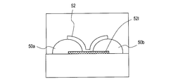
また、図5に示すように、液晶パネルから延びる配線52lと一対の凸部50a、50b(凸部50)の上に形成される凹部電極52とは、典型的には、別の工程で形成される。この場合、配線52lをソースまたはゲートバスラインと同層に形成し、その後、凸部50を形成した後に、凹部電極52を配線52lと電気的に接続するように設ければ良い。このような構成では、配線52lが凸部50の下層に設けられるため、凸部50の形状に依存することなく、配線52lを所望のパターンで形成することができる。例えば図4(c)に示すような構造を得るためには、所定のパターンで設けられた配線上に凸部50を形成し、その後、凸部50を部分的に覆い、かつ、配線と適切な電気的接続が得られるように、凹部電極52を所望のパターンで形成すればよい。
なお、図5には、一対の凸部50a、50b間で、配線52lと凹部電極52との電気的接続が形成されている形態が示されているが、これに限らず任意の接続形態であってよい。例えば、凸部50を含む樹脂層を配線上にわたって形成するとともに、この樹脂層の任意の位置に設けたコンタクトホールを介して配線52lと凹部電極52との電気的接続がとられる形態であってもよい。
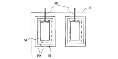
また、図6に示すように、凸部50xは、バンプ電極が有する底面部の4辺のエッジと対向する4つの線状部分から構成される矩形環状の形状を有していてもよい。本明細書では、このように矩形環状の凸部が形成されている場合に、この凸部を形成する部分のうちの対向する二辺を、一対の凸部と表現することがある。
再び図1および2を参照して、液晶モジュール100の端子領域11aにおける、ACF31を用いたICチップ24の実装工程を以下に説明する。
まず、端子領域11aにおいて接続端子51が形成された配線基板11上にACF31が付与され、次いで、配線基板11と駆動用ICチップ24との位置合わせが行われる。その後、圧着ツールなどを用いて、駆動用ICチップ24側より加熱圧着が施される。圧着条件は、例えば、温度160℃~210℃、加圧力40MpPa~100MPa、加圧時間5秒~20秒である。
加熱圧着されることで、接続端子51とバンプ電極54との間に挟まれた導電性粒子は弾性変形(扁平)し、その周りの絶縁性接着材が硬化することで、変形状態を保持したまま固定されることとなる。その結果、接続端子51とバンプ電極54との導通が確保され、電気的接続が実現される。このようにしてACF31を加熱圧着することで、ICチップ24と配線基板11との電気的接続を形成しながら、駆動用ICチップ24が配線基板11上に固着される。
本実施形態で用いられるACF31は、導電性粒子を絶縁性接着材中に混在させることで得ることができる。導電性粒子の粒子径は例えば2~3μmであり、導電性粒子の充填密度は例えば55000~60000個/mm2に設定される。また、導電性粒子としては、プラスチック球にニッケルめっきを施した後、金メッキを施して形成されたものを用いることができる。絶縁性接着材は、例えば、重量平均分子量が1万~10万の範囲内のエポキシ樹脂と、重量平均分子量が1000以下のエポキシ樹脂と、硬化剤とを含有している。このような材料からなるACF31は、硬化後のヤング率が1.4GPa~2.0GPaであり、また、硬化後のガラス転移温度が110℃~135℃である。
ただし、本実施形態の構成によれば、バンプ電極54と接続端子51(凹部電極52)との接続領域が線状に形成されており、より低い荷重でこれらの電気的接続を好適に得ながら接着を行うことが可能であるため、上述のようなACF31を必ずしも用いる必要はない。すなわち、より小さく弾性に乏しい導電性粒子を含む樹脂層(接着層)を用いたり、後述するように導電性粒子を含まない樹脂層を用いることも可能である。
次に、図7(a)および(b)を参照しながら、図2に示したICチップ24のバンプ電極54と、配線基板11の接続端子51との接続の形態を説明する。
図7(a)に示すように、ACF31からなる異方性導電層を介してバンプ電極54と接続端子51との電気的接続を形成する場合、バンプ電極54の側面やエッジ部と、凸部50上の凹部電極52(図7(a)には図示せず)の側面とが接続される。なお、ACF31の代わりにACPを用いても同様である。このようにACF/ACPを用いる場合は、バンプ電極54と凹部電極52とに挟まれる導電性粒子33の斜め方向の弾性変形を利用して接続を実現することが可能である。
ACF31を用いてICチップ24を圧着する工程において、バンプ電極54と凹部電極52と間に介在する導電性粒子33には集中して力が働く。これは、バンプ電極54と凹部電極52とが、バンプ電極54のエッジ部や側面部で選択的に接続される(すなわち、バンプ電極54は、典型的にはエッジ部や側面部のみで凹部電極52と接触する)ように構成されているからである。このとき、凹部電極52とバンプ電極54との接続領域は、凸部50の延びる方向に沿って線状に形成される。この場合、バンプ電極の底面全体にわたって接続が行われる従来の構成に比べて、より少ない荷重でACF31の導電性粒子33を弾性変形させて電気的接続を得ることが可能である。
また、図7(a)に示すように、除冷後におけるACF31の樹脂材料によって生じる収縮力Cを、バンプ電極54と接続端子51(図2参照)との接続方向に働く力のベクトルとして利用することができる。
本実施形態では、バンプ電極54のエッジが凸部50の側面で接続する構成とされているため、バンプ電極の底面と面状接続端子とが接合する場合に比べて、ACF31の樹脂層の厚さが大きくなっている。このように、ACF31の樹脂層を従来構造より厚くすることで、接着材として機能する樹脂材料の硬化時において、従来に比べて大きい凝集力Bを得ることができる。これにより、低荷重による接続を実現することができる。ここで、凝集力とは、接着材または粘着材の分子間に働く引力を指す。
さらに、本実施形態では、接続領域が線状に形成されており、面接触となる場合に比べて圧着時における樹脂材料の排出性が良いので、樹脂材料が先に硬化することによって導電性粒子33への荷重が阻害されることが抑制され、これによって、導電性粒子33の押し込み不足を改善することができる。
本実施形態では、バンプ電極54が、凸部50の側面(斜面)において接続端子51と接続されることが重要である。このため、凹部電極52は、少なくとも凸部50(あるいは凹部60)の側面に設けられていることが好ましい。また、従来の構成とは異なり、バンプ電極54の下部に位置する導電性粒子33の変形は不十分でも良い。このバンプ電極54の底面での接続は、補助的なものと考えることができる。
以上に説明したような構成では、細幅となったバンプ電極54が、左右から挟まれる形態で一対の凸部50が形成する凹部60において支持され、かつ、凸部50(または凹部60)の側面などにおいて電気的接続が形成される。電気的接続が得られる接続領域(バンプ電極54のエッジ)は、好ましくは、凸部50の延びる方向に沿って、線状に形成される。この構成では、圧着時にバンプ電極54を配線基板11に対して強く押し付ける必要がなく、バンプ電極54や、基板11に働く荷重を軽減することができる。したがって、バンプ電極54の変形などを防止しながら、接続の確実性を向上させることができる。
このようにして、配線基板上に設けた一対の凸部から形成される凹部においてバンプ電極との接続を図る構成によれば、バンプ電極が狭ピッチ化したときにも接続の確実性を確保することができる。この構成は、バンプ電極または接続端子の配列ピッチが20μm以下の場合に特に効果的であり、13μm以下の場合にはさらに効果的である。
また、バンプ電極54の側面またはエッジ部と、接続端子51の凹部60の側面とが接続する形態において、接続材としてACFやACPだけではなく、NCFやNCPを用いることも可能である。ただし、NCFやNCPなどの非導電性接着材を用いる場合には、凸部50が所定の弾性力を有する材料から形成されていることが好ましい。
図7(b)は、NCFやNCPなどの非導電性接着材を用いた場合の接続形態を示す。NCF(またはNCP)35がICチップ24と配線基板11との間に介在する場合、バンプ電極54のエッジ部や側面部が、弾性力を有する凸部50を弾性変形させながら凸部50上の凹部電極52(図7(b)には図示せず)に直接密着する。これによりバンプ電極54と凹部電極52とが電気的に接続される。
したがって、従来のような比較的直径の大きい導電性粒子を含む異方性導電層を接着層として用いる必要がなく、導電性粒子を含まない接着層、あるいは、より粒径の小さい導電性粒子を含む接着層を用いることが可能であり、端子を狭ピッチで設ける場合にも端子間リークの発生を抑制することができる。
なお、粒径が小さく比較的硬い導電性粒子を含む接着層を用いる場合には、端子間リークの発生を抑制する他に次のような利点も得られる。すなわち、上述のようにして配線基板上に凹部電極52を設けるが、凹部電極52の材料によっては、その表面に酸化膜や水酸化膜などの非常に薄い高抵抗膜が形成されることがある。この場合に、例えば1μmのニッケル粒子からなる導電性粒子を含む接着層を用いてチップ実装を行うと、導電性粒子が上記高抵抗膜を突き破ることができるので、バンプ電極54と凹部電極52との電気的接続性を向上させることができる。
また、凸部50が弾性に富んだ材料から形成されている場合、チップ実装後に吸湿や熱によって接着材が膨張したときにも、弾性変形していた凸部50がバンプ電極54の方向に復元し得るので、電気的接続の安定性が保たれる。また、バンプ電極54の高さに差がある場合にも、この差を凸部50の弾性変形によって吸収し、それぞれの端子において好適な電気的接続を得ることが可能である。
なお、ACFやACPを用いる場合には、接続端子51が弾性を有していなくても、ACFやACPに分散されている導電性粒子の弾性特性によって、接続信頼性を保つことが可能である。このため、弾性に乏しい材料で凸部50が形成されていてもよい。
以下、図8および図9を参照して、上述したチップ実装構造の変形例を説明する。図8に示す変形例では、実装される1つのICチップ24に対応する複数の接続端子51が設けられている領域の端部において、中央部におけるよりも接続端子51の配列ピッチP1を小さくしている。通常、ICチップ24のバンプ電極54のピッチP0は一定である。ここで、端部においてのみ接続端子51の配列ピッチP1を小さくしていると、圧着時には、中央部へとICチップ24を水平方向に移動させる力が働く。この力がICチップ24の両サイドから付与されて釣り合いがとられるため、ICチップ24と接続端子51との位置合わせが適切に行われやすい。
このようなICチップ24と接続端子51との位置合わせは、図9に示すように、凸部50の大きさ(高さ)をチップ実装領域内で変化させることによっても実現できる。外側(端部)における凸部50dを高くし中心方向の凸部50eを低くすれば、ICチップ24を配線基板11に対して押圧する際に、ICチップ24の両端から中心へと向かう力が働く。
図8および図9に示したこれらの構造では、チップ実装時に凹部60にバンプ電極54が入り込むような挙動を示すため、配線基板11に対するICチップ24のセルフアライメントが実現される。したがって、配線基板11とICチップ24との位置合わせをより容易に行うことができる。
以上説明したように、液晶モジュールの端子領域において、好適には表面が所定の弾性を有する凹状の接続端子を配線基板が具備することにより、バンプ電極のエッジと弾性体による窪みの側面を接合できるような構造が採られる。このことにより、ICチップ長手方向における接着材(樹脂層)の硬化収縮力や、バンプエッジによる応力集中を利用して、バンプ電極と接続端子とを導通させることが可能である。これにより、低荷重(ほぼ無負荷)で接続し得るため、バンプ電極の変形や、異方性導電層中の導電粒子のめり込みの発生を低減することができる。
接続端子を構成する凸状の弾性体としては、ポリイミド、アクリル樹脂、感光性樹脂等を用いることができる。また、バンプ電極と接続端子との間に介在する接着材としては、ACF、ACP、NCF、NCP以外にも、Ni粒子または金属ナノ粒子(例えば直径約1μm以下)を含む樹脂材料を用いることができる。
ACFやACPを使用する場合は、配線基板上の接続端子を構成する凸部は弾性を有していなくてもよい。また、上述したように、一列配列だけでなく、複数の千鳥配列からなる端子群とすることも可能である。なお、接続端子の製造においては、反射型または半透過型の液晶表示装置の一般的製造工程を利用できる。ただし、必要に応じて、凸部を形成するための弾性体樹脂層形成プロセスなどが設けられる。
上記実施形態では、液晶表示装置における駆動用ICチップの実装構造を説明したが、本発明は、この実施形態に限られず、半導体チップ(例えば、ICチップやLEDチップ)を回路基板にフェイスダウン実装する構造に広く適用することができ、狭ピッチの場合にも、端子間の短絡を抑制しつつ、接続信頼性を向上させることができる。本発明の配線基板に半導体チップを実装することで得られる電子回路基板は、例えば液晶表示装置、有機EL表示装置またはイメージセンサなど、様々な電子機器において好適に使用される。
また、配線基板上に形成する接続端子の配列は、実装するチップの端子(電極)の配列に対応するように任意のものとすることができる。長方形状のドライバIC用チップだけでなく、例えば正方形状のチップにおいて電極がアレイ状に設けられた形態のチップに対しても適用できる。
本発明の実施形態は、表示装置に用いられる液晶モジュールにおいて駆動用ICチップをCOG実装するために好適に利用される。本発明の実施形態は、液晶モジュールに限られず、有機ELモジュールなどにも適用することができる。また、本発明の実施形態にかかる表示装置は、プラズマディスプレイパネルやフィールドエミッションディスプレイなどであり得る。
100 液晶モジュール
11 配線基板
12 対向基板
13 液晶層
14 シール部
24 駆動用ICチップ
31 異方性導電フィルム(ACF)
33 導電性粒子
50 一対の凸部
51 接続端子
52 凹部電極
54 バンプ電極
60 凹部
11 配線基板
12 対向基板
13 液晶層
14 シール部
24 駆動用ICチップ
31 異方性導電フィルム(ACF)
33 導電性粒子
50 一対の凸部
51 接続端子
52 凹部電極
54 バンプ電極
60 凹部
Claims (13)
- 基板と、前記基板上に形成された、配線、回路素子、および前記回路素子に前記配線を介して接続された接続端子とを備える配線基板と、
前記接続端子を介して前記配線基板上に実装された半導体チップと
を備える電子回路基板であって、
前記配線基板の前記接続端子は、
一対の凸部であって、それらの間に凹部を形成する一対の凸部と、
前記凹部において設けられ、前記一対の凸部のそれぞれの少なくとも一部を覆う凹部電極とを有しており、
前記半導体チップは、前記接続端子の前記凹部電極と接続されるバンプ電極を有しており、
前記凹部電極と前記バンプ電極との接続領域が線状に形成されている、電子回路基板。 - 前記一対の凸部のそれぞれは第1の方向に沿って延びており、前記線状の接続領域の延びる方向は前記第1の方向と平行である請求項1に記載の電子回路基板。
- 前記凹部電極と、前記バンプ電極とは、前記接続領域において、少なくとも部分的に直接接続されている請求項1または2に記載の電子回路基板。
- 前記バンプ電極は、前記バンプ電極の底面を規定するエッジを有しており、前記接続領域において前記凹部電極と前記バンプ電極の前記エッジとが接続される請求項1から3のいずれかに記載の電子回路基板。
- 前記凹部電極と前記バンプ電極との周辺に配置される樹脂材料層をさらに含み、前記樹脂材料層は、NCFまたはNCPから形成されている請求項1から4のいずれかに記載の電子回路基板。
- 前記一対の凸部は弾性を有する請求項1から5のいずれかに記載の電子回路基板。
- 前記一対の凸部のそれぞれは凸状曲面を表面に有し、少なくとも前記凸状曲面によって前記凹部が形成されている請求項1から6のいずれかに記載の電子回路基板。
- 単一の前記半導体チップの実装領域において、複数の前記接続端子が所定方向に沿って並ぶように設けられており、
前記実装領域の端部における前記接続端子の配列ピッチは、前記実装領域の中央部における前記接続端子の配列ピッチよりも狭い請求項1から7のいずれかに記載の電子回路基板。 - 単一の前記半導体チップの実装領域において、複数の前記接続端子が所定方向に沿って並ぶように設けられており、
前記実装領域の端部に設けられた前記接続端子が有する一対の凸部において、前記実装領域の端部側の一方の凸部が、前記実装領域の中央部側の他方の凸部よりもサイズが大きい請求項1から7のいずれかに記載の電子回路基板。 - 前記回路素子は、TFTと、前記TFTに電気的に接続された画素電極とを有し、
前記配線は、前記接続端子と前記TFTとを接続するゲートバスラインおよびソースバスラインを含む請求項1から9のいずれかに記載の電子回路基板。 - 請求項1から10のいずれかに記載の電子回路基板と、
前記電子回路基板によって駆動される表示媒体層と
を備える表示装置。 - 前記電子回路基板と対向して配置される対向基板をさらに有し、
前記電子回路基板と前記対向基板との間に前記表示媒体層としての液晶層が挟持されている請求項11に記載の表示装置。 - 基板と、前記基板上に形成された、配線、回路素子、および前記回路素子に前記配線を介して接続された接続端子とを備える配線基板であって、前記接続端子のそれぞれは、
一対の凸部であって、それらの間に凹部を形成する一対の凸部と、
前記凹部において設けられ、前記一対の凸部のそれぞれの少なくとも一部を覆う凹部電極とを有し、
前記一対の凸部が形成する一対の斜面によって前記凹部が形成されており、前記一対の斜面において半導体チップのバンプ電極が前記凹部電極と選択的に接続されるように構成されている配線基板。
Priority Applications (1)
| Application Number | Priority Date | Filing Date | Title |
|---|---|---|---|
| US14/002,346 US9148957B2 (en) | 2011-03-04 | 2012-03-01 | Electronic circuit substrate, display device, and wiring substrate |
Applications Claiming Priority (2)
| Application Number | Priority Date | Filing Date | Title |
|---|---|---|---|
| JP2011047452 | 2011-03-04 | ||
| JP2011-047452 | 2011-03-04 |
Publications (1)
| Publication Number | Publication Date |
|---|---|
| WO2012121113A1 true WO2012121113A1 (ja) | 2012-09-13 |
Family
ID=46798079
Family Applications (1)
| Application Number | Title | Priority Date | Filing Date |
|---|---|---|---|
| PCT/JP2012/055266 Ceased WO2012121113A1 (ja) | 2011-03-04 | 2012-03-01 | 電子回路基板、表示装置および配線基板 |
Country Status (2)
| Country | Link |
|---|---|
| US (1) | US9148957B2 (ja) |
| WO (1) | WO2012121113A1 (ja) |
Cited By (1)
| Publication number | Priority date | Publication date | Assignee | Title |
|---|---|---|---|---|
| WO2013129676A1 (ja) | 2012-03-02 | 2013-09-06 | 電気化学工業株式会社 | ポリクロロプレンラテックス、ポリクロロプレンラテックス組成物及び成形品 |
Families Citing this family (15)
| Publication number | Priority date | Publication date | Assignee | Title |
|---|---|---|---|---|
| CN104221471B (zh) * | 2012-04-13 | 2016-07-06 | 株式会社钟化 | 有机el模块以及有机el模块的供电构造 |
| JP2015049435A (ja) * | 2013-09-03 | 2015-03-16 | 株式会社ジャパンディスプレイ | ドライバic、表示装置およびその検査システム |
| JP6528272B2 (ja) * | 2015-04-22 | 2019-06-12 | Tianma Japan株式会社 | 接続用基板および表示装置 |
| WO2017146477A1 (ko) | 2016-02-26 | 2017-08-31 | 서울반도체주식회사 | 디스플레이 장치 및 그의 제조 방법 |
| JP2017175047A (ja) * | 2016-03-25 | 2017-09-28 | ソニー株式会社 | 半導体装置、固体撮像素子、撮像装置、および電子機器 |
| JP7185252B2 (ja) | 2018-01-31 | 2022-12-07 | 三国電子有限会社 | 接続構造体の作製方法 |
| JP7046351B2 (ja) | 2018-01-31 | 2022-04-04 | 三国電子有限会社 | 接続構造体の作製方法 |
| JP7160302B2 (ja) * | 2018-01-31 | 2022-10-25 | 三国電子有限会社 | 接続構造体および接続構造体の作製方法 |
| US20190355277A1 (en) | 2018-05-18 | 2019-11-21 | Aidmics Biotechnology (Hk) Co., Limited | Hand-made circuit board |
| KR102581839B1 (ko) * | 2018-10-02 | 2023-09-22 | 삼성디스플레이 주식회사 | 표시 장치 |
| KR102797110B1 (ko) * | 2019-07-29 | 2025-04-21 | 삼성디스플레이 주식회사 | 표시 장치 |
| KR20210122359A (ko) * | 2020-03-30 | 2021-10-12 | 삼성디스플레이 주식회사 | 표시 장치 및 표시 장치 제조 방법 |
| EP4191644A4 (en) * | 2020-07-27 | 2024-02-07 | Sony Semiconductor Solutions Corporation | ELECTRONIC DEVICE |
| US11906852B2 (en) * | 2022-03-16 | 2024-02-20 | Lumentum Operations Llc | Liquid crystal on silicon panel with electrically-conductive adhesive |
| KR20240034970A (ko) * | 2022-09-07 | 2024-03-15 | 삼성디스플레이 주식회사 | 표시 장치 |
Citations (3)
| Publication number | Priority date | Publication date | Assignee | Title |
|---|---|---|---|---|
| JP2005019895A (ja) * | 2003-06-27 | 2005-01-20 | Denso Corp | フリップチップ実装構造 |
| JP2009088096A (ja) * | 2007-09-28 | 2009-04-23 | Epson Imaging Devices Corp | 実装構造体、電気光学装置、電子部品の実装方法 |
| JP2010027847A (ja) * | 2008-07-18 | 2010-02-04 | Sharp Corp | 半導体素子の実装構造およびそれを備えた表示装置 |
Family Cites Families (14)
| Publication number | Priority date | Publication date | Assignee | Title |
|---|---|---|---|---|
| US5315239A (en) * | 1991-12-16 | 1994-05-24 | Hughes Aircraft Company | Circuit module connections |
| JPH11345302A (ja) | 1998-06-02 | 1999-12-14 | Toppan Printing Co Ltd | Icチップの実装方法、icモジュール、インレットおよびicカード |
| JP2000183490A (ja) | 1998-12-21 | 2000-06-30 | Matsushita Electric Works Ltd | 面実装型電子部品の実装構造 |
| JP4742441B2 (ja) * | 2001-04-16 | 2011-08-10 | 日本電気株式会社 | フレキシブルプリント回路と配線基板との接続構造、その接続方法、液晶表示装置及びその製造方法 |
| JP3952375B2 (ja) | 2002-03-25 | 2007-08-01 | 富士通株式会社 | チップ実装体、チップ実装体の製造方法、及び、電子機器 |
| JP3841087B2 (ja) | 2004-03-17 | 2006-11-01 | セイコーエプソン株式会社 | 電気光学装置用パネル及びその製造方法、電気光学装置、並びに電子機器 |
| JP3835460B2 (ja) * | 2004-04-08 | 2006-10-18 | セイコーエプソン株式会社 | 電子部品実装体の製造方法、及び電気光学装置 |
| JP2007042777A (ja) | 2005-08-02 | 2007-02-15 | Seiko Epson Corp | 半導体装置とその製造方法、回路基板、電気光学装置、及び電子機器 |
| JP5273330B2 (ja) * | 2006-08-04 | 2013-08-28 | 株式会社ジャパンディスプレイ | 表示装置 |
| JP5207163B2 (ja) * | 2007-03-30 | 2013-06-12 | Nltテクノロジー株式会社 | 埋込配線の形成方法、表示装置用基板及び当該基板を有する表示装置 |
| JP5157602B2 (ja) * | 2008-04-03 | 2013-03-06 | セイコーエプソン株式会社 | 電気光学装置及び電子機器 |
| US20120236230A1 (en) | 2009-11-20 | 2012-09-20 | Sharp Kabushiki Kaisha | Device substrate and method for manufacturing same |
| US9760132B2 (en) * | 2013-09-19 | 2017-09-12 | Nvidia Corporation | Stiffening electronic packages by disposing a stiffener ring between substrate center area and conductive pad |
| CN103906358A (zh) * | 2013-11-26 | 2014-07-02 | 番禺得意精密电子工业有限公司 | 电连接器 |
-
2012
- 2012-03-01 US US14/002,346 patent/US9148957B2/en not_active Expired - Fee Related
- 2012-03-01 WO PCT/JP2012/055266 patent/WO2012121113A1/ja not_active Ceased
Patent Citations (3)
| Publication number | Priority date | Publication date | Assignee | Title |
|---|---|---|---|---|
| JP2005019895A (ja) * | 2003-06-27 | 2005-01-20 | Denso Corp | フリップチップ実装構造 |
| JP2009088096A (ja) * | 2007-09-28 | 2009-04-23 | Epson Imaging Devices Corp | 実装構造体、電気光学装置、電子部品の実装方法 |
| JP2010027847A (ja) * | 2008-07-18 | 2010-02-04 | Sharp Corp | 半導体素子の実装構造およびそれを備えた表示装置 |
Cited By (1)
| Publication number | Priority date | Publication date | Assignee | Title |
|---|---|---|---|---|
| WO2013129676A1 (ja) | 2012-03-02 | 2013-09-06 | 電気化学工業株式会社 | ポリクロロプレンラテックス、ポリクロロプレンラテックス組成物及び成形品 |
Also Published As
| Publication number | Publication date |
|---|---|
| US9148957B2 (en) | 2015-09-29 |
| US20130335940A1 (en) | 2013-12-19 |
Similar Documents
| Publication | Publication Date | Title |
|---|---|---|
| WO2012121113A1 (ja) | 電子回路基板、表示装置および配線基板 | |
| CN101060205B (zh) | 平面显示面板及连接结构 | |
| CN1154166C (zh) | 半导体元件的连接结构,使用了该结构的液晶显示装置以及使用了该显示装置的电子装置 | |
| WO2007039959A1 (ja) | 配線基板及びそれを備えた表示装置 | |
| US20120080789A1 (en) | SEMICONDUCTOR CHIP AND MOUNTING STRUCTURE OF THE SAME (as amended) | |
| JP2011198779A (ja) | 電子回路装置、その製造方法及び表示装置 | |
| CN101090101A (zh) | Ic芯片封装和使用该ic芯片封装的图像显示装置 | |
| CN113193017B (zh) | 显示面板和显示装置 | |
| JP4548459B2 (ja) | 電子部品の実装構造体 | |
| CN100479139C (zh) | 驱动器芯片和显示设备 | |
| US20090039495A1 (en) | Wiring substrate and display device including the same | |
| JP2016127259A (ja) | 表示装置 | |
| JP2012227480A (ja) | 表示装置及び半導体集積回路装置 | |
| CN101587874B (zh) | 具有驱动集成电路的芯片及其对应的液晶显示器 | |
| JP4067502B2 (ja) | 半導体装置、半導体装置の実装構造およびそれを備える電子機器ならびに表示装置 | |
| US10937722B1 (en) | Device substrate | |
| CN115762329A (zh) | 绑定结构、显示模组及显示装置 | |
| KR101008824B1 (ko) | 고분자 입자가 부착된 전극을 구비한 반도체 디바이스 및이를 이용한 반도체 패키지 | |
| JP3617495B2 (ja) | 半導体素子の接続構造、液晶表示装置及び電子機器 | |
| JP2005121757A (ja) | 基板接続構造、電子部品、液晶表示装置および電子部品の製造方法 | |
| JP5358923B2 (ja) | 電子部品の実装構造 | |
| JP3767622B2 (ja) | 半導体素子の接続構造、液晶表示装置及び電子機器 | |
| JP5333367B2 (ja) | 電気光学装置及び電子モジュール | |
| TWI390691B (zh) | 銲墊、晶片-基板接合之封裝構造及液晶顯示面板 | |
| KR20070097250A (ko) | 이방성도전필름 및 이를 갖는 표시장치 |
Legal Events
| Date | Code | Title | Description |
|---|---|---|---|
| 121 | Ep: the epo has been informed by wipo that ep was designated in this application |
Ref document number: 12755451 Country of ref document: EP Kind code of ref document: A1 |
|
| WWE | Wipo information: entry into national phase |
Ref document number: 14002346 Country of ref document: US |
|
| NENP | Non-entry into the national phase |
Ref country code: DE |
|
| 122 | Ep: pct application non-entry in european phase |
Ref document number: 12755451 Country of ref document: EP Kind code of ref document: A1 |
|
| NENP | Non-entry into the national phase |
Ref country code: JP |