WO2012102232A1 - ステッピングモータの駆動回路、その集積回路およびそれを備える電子機器、ならびに、ステッピングモータの駆動回路の制御方法 - Google Patents
ステッピングモータの駆動回路、その集積回路およびそれを備える電子機器、ならびに、ステッピングモータの駆動回路の制御方法 Download PDFInfo
- Publication number
- WO2012102232A1 WO2012102232A1 PCT/JP2012/051325 JP2012051325W WO2012102232A1 WO 2012102232 A1 WO2012102232 A1 WO 2012102232A1 JP 2012051325 W JP2012051325 W JP 2012051325W WO 2012102232 A1 WO2012102232 A1 WO 2012102232A1
- Authority
- WO
- WIPO (PCT)
- Prior art keywords
- stepping motor
- drive circuit
- abnormality
- excitation current
- signal
- Prior art date
Links
- 238000000034 method Methods 0.000 title claims description 31
- 230000005284 excitation Effects 0.000 claims abstract description 152
- 238000001514 detection method Methods 0.000 claims abstract description 144
- 230000005856 abnormality Effects 0.000 claims description 190
- 230000004044 response Effects 0.000 claims description 4
- 101100408068 Amanita phalloides PHA1 gene Proteins 0.000 abstract description 27
- 208000015476 pseudohypoaldosteronism type 1 Diseases 0.000 abstract description 27
- 102100031438 E3 ubiquitin-protein ligase RING1 Human genes 0.000 abstract description 8
- 101000707962 Homo sapiens E3 ubiquitin-protein ligase RING1 Proteins 0.000 abstract description 8
- 102100037964 E3 ubiquitin-protein ligase RING2 Human genes 0.000 abstract description 4
- 101001095815 Homo sapiens E3 ubiquitin-protein ligase RING2 Proteins 0.000 abstract description 4
- 230000010355 oscillation Effects 0.000 description 26
- 230000008569 process Effects 0.000 description 22
- 238000010586 diagram Methods 0.000 description 17
- 230000007257 malfunction Effects 0.000 description 15
- 230000002265 prevention Effects 0.000 description 15
- 239000003990 capacitor Substances 0.000 description 10
- 102100040836 Claudin-1 Human genes 0.000 description 8
- 101100113671 Homo sapiens CLDN1 gene Proteins 0.000 description 8
- 101100113675 Saccharomyces cerevisiae (strain ATCC 204508 / S288c) CLD1 gene Proteins 0.000 description 8
- 102000012677 DET1 Human genes 0.000 description 7
- 101150113651 DET1 gene Proteins 0.000 description 7
- 101150066284 DET2 gene Proteins 0.000 description 7
- 230000002159 abnormal effect Effects 0.000 description 6
- 230000008901 benefit Effects 0.000 description 4
- 208000012954 congenital vertebral-cardiac-renal anomalies syndrome Diseases 0.000 description 4
- 230000005540 biological transmission Effects 0.000 description 2
- 230000007423 decrease Effects 0.000 description 2
- 230000004048 modification Effects 0.000 description 2
- 238000012986 modification Methods 0.000 description 2
- 230000000630 rising effect Effects 0.000 description 2
- 230000003247 decreasing effect Effects 0.000 description 1
Images


Classifications
-
- H—ELECTRICITY
- H02—GENERATION; CONVERSION OR DISTRIBUTION OF ELECTRIC POWER
- H02P—CONTROL OR REGULATION OF ELECTRIC MOTORS, ELECTRIC GENERATORS OR DYNAMO-ELECTRIC CONVERTERS; CONTROLLING TRANSFORMERS, REACTORS OR CHOKE COILS
- H02P8/00—Arrangements for controlling dynamo-electric motors rotating step by step
- H02P8/34—Monitoring operation
-
- H—ELECTRICITY
- H02—GENERATION; CONVERSION OR DISTRIBUTION OF ELECTRIC POWER
- H02P—CONTROL OR REGULATION OF ELECTRIC MOTORS, ELECTRIC GENERATORS OR DYNAMO-ELECTRIC CONVERTERS; CONTROLLING TRANSFORMERS, REACTORS OR CHOKE COILS
- H02P8/00—Arrangements for controlling dynamo-electric motors rotating step by step
- H02P8/36—Protection against faults, e.g. against overheating or step-out; Indicating faults
- H02P8/38—Protection against faults, e.g. against overheating or step-out; Indicating faults the fault being step-out
-
- H—ELECTRICITY
- H02—GENERATION; CONVERSION OR DISTRIBUTION OF ELECTRIC POWER
- H02P—CONTROL OR REGULATION OF ELECTRIC MOTORS, ELECTRIC GENERATORS OR DYNAMO-ELECTRIC CONVERTERS; CONTROLLING TRANSFORMERS, REACTORS OR CHOKE COILS
- H02P8/00—Arrangements for controlling dynamo-electric motors rotating step by step
- H02P8/36—Protection against faults, e.g. against overheating or step-out; Indicating faults
-
- B—PERFORMING OPERATIONS; TRANSPORTING
- B41—PRINTING; LINING MACHINES; TYPEWRITERS; STAMPS
- B41J—TYPEWRITERS; SELECTIVE PRINTING MECHANISMS, i.e. MECHANISMS PRINTING OTHERWISE THAN FROM A FORME; CORRECTION OF TYPOGRAPHICAL ERRORS
- B41J19/00—Character- or line-spacing mechanisms
- B41J19/18—Character-spacing or back-spacing mechanisms; Carriage return or release devices therefor
- B41J19/20—Positive-feed character-spacing mechanisms
- B41J19/202—Drive control means for carriage movement
Definitions
- the present invention relates to a driving circuit for a stepping motor, an integrated circuit in which the driving circuit is integrated, an electronic apparatus including the integrated circuit, and a method for controlling the driving circuit for a stepping motor, and more specifically, an excitation current from the driving circuit to the stepping motor.
- the present invention relates to a technique for detecting an abnormality in a path that transmits a signal.
- stepping motors that realize smooth rotation without unevenness and enable low vibration and low noise are often used.
- a stepping motor is driven by applying excitation currents whose phases are shifted from each other by 90 ° to a two-phase excitation coil with a waveform close to a sine wave (that is, a pseudo sine wave).
- Patent Document 1 discloses a target voltage generation unit that generates a target voltage that indicates a target value of an excitation current based on a reference voltage that indicates an upper limit value of the excitation current, and based on the target voltage.
- An example of a stepping motor drive circuit including a current control unit for controlling the excitation current is disclosed.
- the drive circuit and the stepping motor are connected to each other by wiring.
- This wiring is connected by connection parts, such as a terminal or a connector, in a drive circuit and a stepping motor. Furthermore, in the middle part of the wiring, the wiring may be connected by a connector or the like.
- connection part of this wiring is loosened, poor contact, or the wiring is disconnected, the excitation current cannot be supplied appropriately from the drive circuit to the excitation coil. Can not be.
- Patent Document 1 Japanese Patent Laid-Open No. 2008-029145
- the present invention has been made to solve such problems, and an object thereof is to provide a stepping motor drive circuit capable of detecting an abnormality in wiring for supplying an excitation current to the stepping motor. That is.
- a driving circuit for a stepping motor includes a target voltage generating unit for generating a target voltage indicating a target value for an exciting current determined based on a reference voltage indicating an upper limit value of an exciting current flowing in the stepping motor, and a target A current control unit that controls the excitation current so that the value of the excitation current is maintained at a target value based on the voltage;
- the current control unit includes a comparison unit for comparing a signal corresponding to the excitation current with a predetermined threshold value.
- the drive circuit further includes an abnormality detection unit for detecting an abnormality in a path through which the excitation current is supplied from the drive circuit to the stepping motor based on an output signal from the comparison unit.
- the comparison unit compares a voltage corresponding to the excitation current with a target voltage as a threshold value.
- the abnormality detection unit detects an abnormality based on the output signal from the comparison unit and the control signal indicating the polarity of the excitation current.
- the stepping motor includes first and second exciting coils.
- the current control unit includes a first channel and a second channel for outputting an excitation current corresponding to each of the first and second excitation coils.
- the current control unit has an abnormality based on the state of the output signal of the other channel at a predetermined timing when the control signal for one of the first and second channels is in a predetermined state. Detect that.
- the current control unit sets the voltage corresponding to the excitation current for the other channel to the target value of the channel.
- the output signal indicates that it has not reached, it is detected that an abnormality has occurred.
- control signal is a pulse signal.
- the predetermined timing is determined based on the falling timing of the control signal.
- the target voltage generation unit generates the target voltage by dividing the reference voltage according to a ratio that changes stepwise from 0 to 1 of the target value with respect to the upper limit value.
- the drive circuit further includes a command generation unit that generates a signal indicating a ratio and a control signal based on information from outside the drive circuit.
- the abnormality detection unit is based on the number of times that the level of the signal corresponding to the excitation current reaches the threshold value within a predetermined period in a state where the excitation current can be output from the drive circuit to the stepping motor. To detect abnormalities.
- the threshold value is determined based on the target value.
- the abnormality detection unit counts the number of times based on the output signal from the comparison unit.
- the abnormality detection unit detects that an abnormality has occurred when the number of times falls below a predetermined reference number.
- the threshold value is determined based on a minimum current value that is different from the target value and that can drive the stepping motor.
- the abnormality detection unit counts the number of times based on the output signal from the comparison unit.
- the threshold value is set based on a value lower than the target value.
- the predetermined period is determined based on at least one of a start signal for the drive circuit, an enable signal for enabling the drive circuit, and a control signal indicating the polarity of the excitation current.
- the abnormality detection unit determines the abnormality in response to the abnormality being continuously detected a predetermined number of times.
- the abnormality detection unit outputs an abnormality signal based on the fact that the abnormality has been confirmed.
- An integrated circuit according to the present invention is obtained by integrating any one of the drive circuits described above.
- An electronic apparatus includes a stepping motor and any one of the drive circuits described above.
- the stepping motor drive circuit control method includes a step of generating a target voltage indicating a target value for an excitation current determined based on a reference voltage indicating an upper limit value of the excitation current flowing in the stepping motor, and a target voltage. Based on this, the step of controlling the exciting current so that the value of the exciting current is maintained at the target value, the step of comparing the signal corresponding to the exciting current with a predetermined threshold, and the output signal by the step of comparing And detecting an abnormality in a path through which an exciting current is supplied from the drive circuit to the stepping motor.
- the comparing step includes a step of comparing a voltage corresponding to the exciting current with a target voltage as a threshold value.
- the step of detecting the abnormality includes a step of detecting the abnormality based on the output signal and a control signal indicating the polarity of the excitation current.
- the method further includes a step of counting the number of times that the level of the signal corresponding to the excitation current reaches the threshold value within a predetermined period in a state where the excitation current can be output from the drive circuit to the stepping motor.
- the step of detecting the abnormality includes a step of detecting the abnormality based on the number of times.
- FIG. 1 is an overall block diagram of a motor drive system including a drive circuit for a stepping motor according to a first embodiment. It is an example of the time chart for demonstrating abnormality detection control in the case of full step mode. It is an example of the time chart for demonstrating abnormality detection control in the case of a half step mode. It is another example of the time chart for demonstrating abnormality detection control in the case of a half step mode.
- FIG. 3 is a functional block diagram for explaining abnormality detection control executed by an abnormality detection unit in the first embodiment. 5 is a flowchart for illustrating details of an abnormality detection control process executed by an abnormality detection unit in the first embodiment.
- FIG. 6 is an overall block diagram of a motor drive system including a drive circuit for a stepping motor according to a second embodiment.
- FIG. 10 is an overall block diagram of a motor drive system including a drive circuit for a stepping motor according to a third embodiment.
- 12 is a first time chart for illustrating abnormality detection control in the third embodiment.
- 10 is a second time chart for illustrating abnormality detection control in the third embodiment.
- it is a functional block diagram for demonstrating abnormality detection control performed by the abnormality detection part.
- 10 is a flowchart for explaining details of an abnormality detection control process executed by an abnormality detection unit in the third embodiment.
- FIG. 10 is an overall block diagram of a motor drive system including a drive circuit for a stepping motor according to a fourth embodiment.
- FIG. 10 is an overall block diagram of a motor drive system including a drive circuit for a stepping motor according to a fifth embodiment.
- 10 is a time chart for explaining abnormality detection control in a fifth embodiment.
- it is a flowchart for demonstrating the detail of the abnormality detection control process performed in an abnormality detection part.
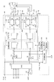
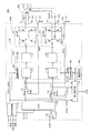
- FIG. 1 is an overall block diagram of a motor drive system 10 including a stepping motor drive circuit 100 according to the first embodiment.
- the motor drive system 10 is used as a drive unit of an electronic device such as a printer, a fax machine, a scanner, or a camera, for example.
- stepping motor 200 is a two-phase stepping motor.
- the stepping motor 200 includes excitation coils L1 and L2 corresponding to two phases, respectively, and a rotor 210.
- Excitation currents IOUT1 and IOUT2 flow through the excitation coils L1 and L2, respectively.
- the drive circuit 100 controls the excitation currents IOUT1 and IOUT2 so that the values of the excitation currents IOUT1 and IOUT2 are maintained at the set values.
- the drive circuit 100 causes the stepping motor to be microstep driven. That is, the drive circuit 100 rotates the rotor 210 of the stepping motor at a step angle smaller than the basic step angle by finely changing the ratio of the excitation currents IOUT1 and IOUT2.
- the drive circuit 100 includes an input buffer 110, a D / A converter (DAC) 120, a current control circuit 130, an abnormality detection unit 170, a PWM control unit 180, and an oscillation circuit 190.
- DAC D / A converter
- the current control circuit 130 includes comparators 131 and 132, a logic control unit 140 including logic circuits 141 and 142, a pre-driver unit 150 including pre-drivers 151 and 152, and H bridges 161 and 162.
- the comparator 131, the logic circuit 141, the pre-driver 151, and the H bridge 161 constitute a circuit corresponding to the channel CH1 that supplies the exciting current IOUT1 to the exciting coil L1.
- the comparator 132, the logic circuit 142, the pre-driver 152, and the H bridge 162 constitute a circuit corresponding to the channel CH2 that supplies the exciting current IOUT2 to the exciting coil L2. Since the configurations and functions of the respective circuits corresponding to channels CH1 and CH2 are the same, in the detailed description of the circuit shown below, description will be made regarding channel CH1, and the same description regarding channel CH2 will not be repeated. .
- the input buffer 110 is a so-called voltage follower circuit and outputs the input reference voltage VREF as it is.
- the reference voltage VREF is a voltage indicating the upper limit value of the excitation currents IOUT1 and IOUT2.
- the D / A converter 120 corresponds to a “target voltage generator” in the stepping motor drive circuit of the present invention.
- the D / A converter 120 receives the reference voltage VREF and the control signals I01 and I11 and outputs the target voltage VA1 for the channel CH1.
- the control signals I01 and I11 are signals for changing the ratio of the set value of the excitation current IOUT1 to the upper limit value of the excitation current IOUT1 between 0 and 1.
- the ratio of the set value of the excitation current IOUT1 to the upper limit value of the excitation current IOUT1 is the combination of the potential levels of the control signals I01 and I11 (H, H), (L, H), (H, L), (L, L) In contrast, for example, it varies between four values of 0%, 33%, 67%, and 100%, respectively.
- the D / A converter 120 generates the target voltage VA1 by dividing the reference voltage VREF according to the above ratio.
- the current control circuit 130 receives the target voltage VA1 and controls the excitation current IOUT1 so that the value of the excitation current IOUT1 is maintained at a set value.
- the comparator 131 compares the voltage RNF1 indicating the current (excitation current IOUT1) flowing through the H bridge 161 converted by the resistor R1 provided outside the drive circuit 100 with the target voltage VA1, and outputs an output signal indicating the comparison result. CLOUT1 is generated. For example, the output signal CLOUT1 is set to high (Hi) when the voltage RNF1 does not reach the target voltage VA1, and is set to low (Lo) when the voltage RNF1 reaches the target voltage VA1.
- the logic circuit 141 receives the control signal PHA1 indicating the polarity of the excitation current IOUT1 and the output signal CLOUT1 of the comparator 131.
- the logic circuit 141 generates a drive signal using these signals and the control signal PWM set by the PWM control unit based on the oscillation signal OSC from the oscillation circuit 190.
- the pre-driver 151 amplifies the drive signal sent from the logic circuit 141. A signal from the pre-driver 151 is given to the H bridge 161. According to the operation of the H bridge 161, the magnitude of the excitation current IOUT1 supplied to the excitation coil L1 changes.
- the logic circuit 141 decreases the excitation current IOUT1.
- the logic circuit 141 increases the excitation current IOUT1 after a lapse of a predetermined time from the start of the operation of decreasing the excitation current IOUT1. By repeating this operation, the value of the excitation current IOUT1 is controlled to be kept at the set value.
- the H bridge 161 includes P-type MOS transistors Q11 and Q12 and N-type MOS transistors Q13 and Q14.
- P-type MOS transistor Q11 and N-type MOS transistor Q13 are connected in series between a power supply node to which power supply potential VM of stepping motor 200 is applied and a terminal T13 to which one end of resistor R1 is connected.
- P-type MOS transistor Q12 and N-type MOS transistor Q14 are connected in series between the power supply node and terminal T13 to which one end of resistor R1 is connected. The other end of resistor R1 is connected to the ground node.
- the node N11 to which the P-type MOS transistor Q11 and the N-type MOS transistor Q13 are connected is connected to the terminal T11.
- node N12 to which P-type MOS transistor Q12 and N-type MOS transistor Q14 are connected is connected to terminal T12.
- the two terminals of the exciting coil L1 are connected to the terminals T11 and T12 through wiring.
- an example of a configuration using an H-bridge formed of a P-type MOS transistor and an N-type MOS transistor has been described.
- an N-type MOS transistor is used for the entire configuration of a transistor that forms an H-bridge. May be.
- the booster circuit for driving the transistors is compared with the case where the P-type MOS transistor and the N-type MOS transistor are used.
- the circuit area of the N-type MOS transistor tends to be smaller than that of the P-type MOS transistor.
- the booster circuit may be included.
- N-type MOS transistors can have the advantage of reducing the overall circuit area.
- a booster circuit becomes unnecessary. Therefore, the type of the transistor forming the H bridge is appropriately selected in consideration of factors such as the current flowing through the circuit and the circuit area.
- the abnormality detection unit 170 receives control signals PHA1 and PHA2 indicating the polarities of the excitation currents IOUT1 and IOUT2, output signals CLOUT1 and CLOUT2 of the comparators 131 and 132, and an oscillation signal OSC from the oscillation circuit 190, respectively. Based on these pieces of information, the abnormality detection unit 170 performs abnormality detection control for detecting whether or not an abnormality has occurred in the wiring that supplies the excitation currents IOUT1 and IOUT2 from the drive circuit 100 to the stepping motor 200.
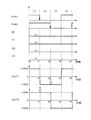
- FIG. 2 shows an example of a time chart in the case of the full step mode
- FIG. 3 shows an example of a time chart in the case of the half step mode. 2 and 3
- the horizontal axis indicates time
- the vertical axis indicates the state of the control signals PHA1 and PHA2 indicating the polarity of the excitation current
- the control signals I01, I11 which determine the voltage division ratio of the target voltage.
- the states of I02 and I12 and the states of excitation currents IOUT1 and IOUT2 are shown.
- control signals I01, I11, I02, and I12 are always set to a low level (Lo), and excitation currents IOUT1 and IOU2 are controlled by control signal PHA1.
- a square wave shape is switched between a + 100% state and a -100% state.
- the excitation current IOUT1 is switched from + 100% to ⁇ 100% as the control signal PHA1 falls from the high level to the low level at time t1, and is controlled at time t3. As the signal PHA1 rises from the low level to the high level, the exciting current IOUT1 is switched from ⁇ 100% to + 100%.
- the excitation current IOUT2 has a phase difference of 90 ° from the excitation current IOUT2, the excitation current IOUT2 is switched from + 100% to ⁇ 100% at time t2, and the excitation current IOUT2 is ⁇ 100 at time t4. From% to + 100%.
- the output signal CLOUT2 of the comparator 132 is in the Lo state.
- the output signal CLOUT2 of the comparator 132 is in the Hi state.
- the timing of detecting the state of the output signal of the comparator may be either when the control signals PHA1 and PHA2 rise or fall. Alternatively, the timing for detecting the state of the output signal of the comparator may be after a predetermined delay time has elapsed from the rise or fall of the control signals PHA1 and PHA2.
- the states of the control signals I01, I11, I02, and I12 are changed for half the quarter period (ie, 1/8 period) when the combination state of the excitation currents IOUT1 and IOUT2 changes. Be controlled.
- control signals I01 and I11 are set to the Hi state only from time t22 to time t23 and from time t26 to time t27 in FIG.
- control signals I02 and I12 are set to the Hi state only from time t20 to time t21 and from time t24 to time t25 in FIG.
- the excitation currents IOUT1 and IOUT2 are in the 0% state, and the excitation currents IOUT1 and IOUT2 are The waveform can be made closer to a sine wave.
- the current state of the other channel is detected by detecting the current state of the other channel. It can be determined whether or not an abnormality has occurred in the wiring.
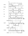
- FIG. 4 shows an example in which the control signals I01 and I02 are set to become Lo for 1/8 period and the control signals I11 and I12 are set to Hi for 1/8 period.
- the excitation current level is + 67% between time t31 and time t32, between time t33 and time t34, between time t35 and time t36, and between time t37 and time t38 in FIG.
- An intermediate state of ⁇ 67% can be obtained, and the excitation current can be made closer to a sine wave.
- the timing at which the states of the control signals PHA1, PHA2 are just switched is also the timing at which the level of the excitation current changes to + 100% (or to -100%). For this reason, there is a possibility that a state during charging of the exciting coil is detected and an abnormality cannot be appropriately detected. In such a case, as described above, it is preferable to detect a state after a predetermined delay time from the timing at which the states of the control signals PHA1 and PHA2 are switched.
- control signals I01, I11, I02,... are further output for 1/4 of the 1/4 cycle (that is, 1/16 cycle) in which the polarity combination state of the excitation currents IOUT1, IOUT2 changes.
- the level of the excitation current can be further set to + 33% or ⁇ 33% by the combination of the control signals I01, I11, I02, and I12. Thereby, the waveform of the excitation current can be made closer to a sine wave, and smoother rotation can be realized.
- an abnormality occurs in the wiring of the other channel by detecting the current state of the other channel at an appropriate timing based on the timing at which the control signals PHA1 and PHA2 are switched. It can be determined whether or not.
- FIG. 5 is a functional block diagram for explaining the abnormality detection control executed by the abnormality detection unit 170 in the first embodiment.
- Each functional block described in the functional block diagram of FIG. 5 is realized by hardware or software processing by the abnormality detection unit 170.
- abnormality detection unit 170 includes a current limit detection unit 171, a determination unit 172, and a malfunction prevention unit 173.
- the current limit detection unit 171 receives the oscillation signal OSC from the oscillation circuit 190 and the output signals CLOUT1 and CLOUT2 from the comparators 131 and 132. For each of the output signals CLOUT1 and CLOUT2, the current limit detection unit 171 determines whether or not the output signals CLOUT1 and CLOUT2 become Lo during a predetermined period (T1) determined from the oscillation signal OSC, that is, the output signals CLOUT1 and CLOUT2. It is determined whether CLOUT2 reaches the target voltages VA1 and VA2, respectively, and whether the excitation currents IOUT1 and IOUT2 have reached current limit values corresponding to the target voltages VA1 and VA2.
- T1 predetermined period
- the current limit detection unit 171 sets the corresponding detection signals CLD1 and CLD2 to OFF when the output signals CLOUT1 and CLOUT2 become Lo during the predetermined period. On the other hand, when the output signals CLOUT1 and CLOUT2 remain Hi during the predetermined period, the detection signals CLD1 and CLD2 are set to ON. Then, current limit detection unit 171 outputs detection signals CLD1 and CLD2 to determination unit 172.
- Determination unit 172 receives detection signals CLD1, CLD2 and control signals PHA1, PHA2 from current limit detection unit 171. As described with reference to FIGS. 2 to 4, the determination unit 172 sets the detection signals CLD1 and CLD2 of the other channel to ON at a predetermined timing determined based on the rise or fall of the control signals PHA1 and PHA2. It is determined whether or not.
- the determination unit 172 may have an abnormality in the wiring of the other channel. As a result, the abnormality flags DET1 and DET2 of the corresponding channel are set to ON. When the detection signals CLD1, CLD2 are off, the abnormality flags DET1, DET2 are set off.
- the determination unit 172 outputs the abnormality flags DET1 and DET2 to the malfunction prevention unit 173.
- the malfunction prevention unit 173 is temporarily determined to be abnormal by the determination unit 172 even though there is originally no wiring abnormality due to, for example, a delay in the excitation current rising due to the operating state of the stepping motor 200 or the influence of noise. This is a function to prevent the influence of false detection in the case of failure.
- the malfunction prevention unit 173 receives the abnormality flags DET1, DET2 and the control signals PHA1, PHA2 from the determination unit 172.
- the malfunction prevention unit 173 determines whether or not the abnormality flags DET1 and DET2 are continuously set to ON in the determination unit 172 at a predetermined predetermined number of times (for example, three times) of the control signals PHA1 and PHA2.
- the malfunction prevention unit 173 detects that the abnormality flags DET1 and DET2 are set to ON continuously for a predetermined number of times, the malfunction prevention unit 173 determines that a wiring abnormality has occurred, and in response thereto, an abnormality signal Outputs ALM.
- the abnormality signal ALM is received by an abnormality notification unit (not shown) provided outside or inside the drive circuit 100, and the occurrence of abnormality is notified to the user.
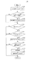
- FIG. 6 is a flowchart for explaining details of the abnormality detection control process executed by the abnormality detection unit 170 in the first embodiment.
- a program stored in advance in the CPU is called from the main routine, and The processing is realized by being executed periodically.
- dedicated hardware electronic circuit
- abnormality detection unit 170 outputs signals CLOUT1 and CLOUT2 (hereinafter referred to as CLOUT1 and CLOUT2) from comparators 131 and 132 at step (hereinafter abbreviated as S) 100. Collectively also referred to as “CLOUT”). Then, in S110, the abnormality detection unit 170 determines whether or not these output signals are in a Hi state for a predetermined period T1.
- abnormality detection unit 170 detects detection signal CLD (hereinafter, CLD1, CLD2) for the corresponding channel in S120. Are also collectively referred to as “CLD”). Thereafter, the process proceeds to S130.
- CLD detection signal
- the abnormality detection unit 170 determines whether or not there is a predetermined detection timing based on a control signal PHA (hereinafter, PHA1 and PHA2 are also collectively referred to as “PHA”).
- PHA1 and PHA2 are also collectively referred to as “PHA”.
- the abnormality detection unit 170 ends the process.
- abnormality detection unit 170 determines whether or not detection signal CLD of the other channel is set to ON. .
- the abnormality detection unit 170 determines that the exciting current is equal to the target value and no wiring abnormality has occurred, and ends the process. To do.
- abnormality detection unit 170 determines that there is a possibility that a wiring abnormality has occurred.
- the abnormality flag DET (hereinafter, DET1 and DET2 are collectively referred to as “DET”) is set to ON.
- the abnormality detection unit 170 determines whether or not the abnormality flag DET has been detected for a predetermined number of cycles (n times: n is a natural number) of the control signal PHA.
- abnormality detection unit 170 terminates the process as an erroneous detection of an abnormal state.
- control signal PHA is detected n times consecutively (YES in S160)
- the process proceeds to S170, and abnormality detection unit 170 determines that a wiring abnormality has occurred. Then, abnormality detection unit 170 outputs abnormality signal ALM in S180.
- Embodiment 2 a stepping motor drive circuit having a function of internally generating the above-described control signal based on information such as a control mode given from the outside will be described.
- FIG. 7 is an overall block diagram of a motor drive system 10A including a stepping motor drive circuit 100A according to the second embodiment.
- FIG. 7 shows a configuration in which a command generation unit 115 is added to the drive circuit 100 described in FIG. 1 of the first embodiment. In FIG. 7, the description of the elements overlapping with those in FIG. 1 will not be repeated.
- drive circuit 100A further includes a command generation unit 115 in addition to the configuration of drive circuit 100 shown in FIG.
- the command generation unit 115 receives a reference clock signal CLK, a control mode signal MOD, a signal CW_CCW indicating a rotation direction, and an enable signal ENB from the outside of the circuit.
- the control mode signal MOD is a signal that determines which of the full step mode, the half step mode, and the quarter step mode described with reference to FIGS. 2 to 4 of the first embodiment is selected.
- the command generation unit 115 generates control signals PHA1 and PHA2 based on these pieces of information, and outputs them to the logic control unit 140 and the abnormality detection unit 170. Further, the command generator 115 generates control signals I01, I11, I02, and I12 and outputs them to the D / A converter 120.
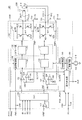
- FIG. 8 is an overall block diagram of a motor drive system 10B including a stepping motor drive circuit 100B according to the third embodiment.
- the abnormality detection unit 170 in FIG. 1 of the first embodiment is replaced with the abnormality detection unit 170B, and a resistor R10 and a capacitor C10 connected in parallel provided outside the drive circuit are connected to the oscillation circuit 190. It has become a thing.
- drive circuit 100B receives a power save signal PS that is a start signal from the outside.
- the drive circuit 100B is powered on by supplying power to each circuit in the drive circuit 100B.
- the power save signal PS is turned off (low level)
- the standby state is entered, and the output of the excitation current to the stepping motor 200 is stopped.
- the logic circuit 141 of the channel CH1 receives the phase signal PHA1 indicating the polarity of the excitation current IOUT1, the output signal CLOUT1 of the comparator 131, and the enable signal ENB. Then, the logic circuit 141 generates a drive signal using these signals and a control signal PWM set by the PWM control unit based on the oscillation signal OSC from the oscillation circuit 190.
- the enable signal ENB is a signal for enabling the logic control unit 140 (logic circuits 141 and 142).
- the enable signal ENB When the enable signal ENB is turned on (high level), the logic control unit 140 is enabled and H When the transistors included in the bridges 161 and 162 are driven, an excitation current is supplied from the drive circuit 100B to the stepping motor 200.
- the enable signal ENB is turned off (low level)
- the logic control unit 140 is disabled, and the supply of the excitation current from the drive circuit 100B to the stepping motor 200 is stopped.
- the oscillation circuit 190 is connected to a resistor R10 and a capacitor C10 connected in parallel.
- the period of the chopping operation as will be described later with reference to FIG. 10 is determined by the parallel circuit of the resistor R10 and the capacitor C10.
- the abnormality detector 170B includes phase signals PHA1 and PHA2 indicating the polarities of the excitation currents IOUT1 and IOUT2, output signals CLOUT1 and CLOUT2 of the comparators 131 and 132, an oscillation signal OSC from the oscillation circuit 190, and an enable signal ENB.
- the power save signal PS is received. Based on this information, the abnormality detection unit 170B executes abnormality detection control for detecting whether or not an abnormality has occurred in the wiring that supplies the excitation currents IOUT1 and IOUT2 from the drive circuit 100B to the stepping motor 200.
- FIG. 9 shows a time chart showing a general output current in the case of the full step mode as an example.
- the horizontal axis represents time, and the vertical axis represents the states of the phase signals PHA1 and PHA2 indicating the polarity of the excitation current, the states of the control signals I01, I11, I02, and I12 that determine the voltage division ratio of the target voltage, and the excitation current IOUT1. , IOUT2 is shown.
- the case of the full step mode will be described as an example.
- each control signal is only output for a half of a quarter period (that is, a 1/8 period) during which the combination state of the polarities of the excitation currents IOUT1 and IOUT2 changes.
- a half step mode in which the states of I01, I11, I02, and I12 are controlled, or for a quarter (ie, 1/16 period) of a quarter period in which the combination state of the polarity of the excitation currents IOUT1 and IOUT2 changes.
- the quarter step mode for controlling the states of the control signals I01, I11, I02, and I12 the following control can be applied.
- control signals I01, I11, I02, and I12 are always set to a low level (Lo), and excitation currents IOUT1 and IOU2 are applied to phase signals PHA1 and PHA2, respectively. Synchronously, it switches to a square waveform between + 100% and ⁇ 100%.
- the excitation current IOUT1 switches from + 100% to ⁇ 100% as the phase signal PHA1 falls from the high level to the low level at time t41, and the phase at time t43. As the signal PHA1 rises from the low level to the high level, the exciting current IOUT1 is switched from ⁇ 100% to + 100%.
- the excitation current IOUT2 has a phase difference of 90 ° from the excitation current IOUT2, the excitation current IOUT2 is switched from + 100% to ⁇ 100% at time t42, and the excitation current IOUT2 is ⁇ 100 at time t44. From% to + 100%.
- an excitation current closer to a sine wave can be supplied than in the full step mode of FIG. 9 by using an intermediate level excitation current.
- FIG. 10 is a diagram for explaining in more detail the state of the excitation current IOUT1 from time 0 to time t41 in FIG. 9, for example.
- the horizontal axis represents time
- the vertical axis represents excitation current IOUT, voltage RNF indicating excitation current IOUT, oscillation signal OSC, and output signal CLOUT.
- the signals for channels CH1 and CH2 are generically named, for example, IOUT1 and IOUT2 are referred to as “IOUT” or the like.
- the output current IOUT is controlled to be the target current IREF by using a feedback loop as shown in FIG.
- the oscillation signal OSC changes in a triangular waveform between the potential VCRH and the potential VCRL by the parallel circuit of the resistor R10 and the capacitor C10 shown in FIG. More specifically, when the oscillation signal OSC becomes the potential VCRL, the capacitor C10 of the parallel circuit is charged, and the oscillation signal OSC increases to the potential VCRH. When the oscillation signal OSC becomes the potential VCRH, the charging of the capacitor C10 is stopped, and the charge stored in the capacitor C10 is discharged by the resistor R10. When the potential of the oscillation signal OSC decreases to the potential VCRL due to this discharge, the capacitor C10 is charged again.
- the chopping cycle TCH of the current control circuit 130 is determined by the resistor R10 and the capacitor C10 of the parallel circuit.
- the output signal CLOUT is turned on, and the logic control unit 140 and the pre-driver unit 150 start driving the H-bridge transistor.
- the excitation current IOUT increases.
- the voltage RNF increases.
- the output signal CLOUT remains on and the supply of the excitation current IOUT is continued.
- the output signal CLOUT from the comparator is turned off (time t51, t53, t55, t57).
- the driving of the H bridge is stopped by the logic control unit 140. Then, since no current flows through the resistors R1 and R2, the voltage RNF is lowered to the ground potential.
- the oscillation signal OSC rises again after the oscillation signal OSC has dropped to the potential VCRL, the output signal CLOUT is turned on, the H bridge is driven, and the output current IOUT increases.
- the phase signal PHA indicating the polarity of the excitation current IOUT and the control signals I01, I02, I11, and I12 indicate the target current IREF.
- the output current IOUT is always controlled to be a predetermined target current IREF by repeating the chopping operation as described above in a short chopping cycle TCH.
- the voltage RNF reaches the target voltage VA in each chopping cycle TCH, that is, the excitation current IOUT is the current.
- the target current IREF which is a limit
- the output signal CLOUT is turned off from on.
- the excitation signal IOUT does not reach the current limit, and the output signal CLOUT remains on.
- the path through which the excitation current is supplied by detecting whether the excitation current IOUT has reached the current limit, that is, whether the output signal CLOUT has changed from on to off. Detect abnormalities.
- FIG. 11 is a functional block diagram for explaining the abnormality detection control executed by the abnormality detection unit 170B in the third embodiment.
- Each functional block described in the functional block diagram of FIG. 11 is realized by hardware or software processing by the abnormality detection unit 170B.
- abnormality detection unit 170B includes a current limit detection unit 171B, a determination unit 172B, and a malfunction prevention unit 173B.
- the current limit detection unit 171B receives the oscillation signal OSC from the oscillation circuit 190 and the output signal CLOUT from the comparator. For the output signal CLOUT, the current limit detection unit 171B determines whether or not the output signal CLOUT has been turned from on to off during each chopping period described in FIG. 10, that is, the output signal CLOUT has reached the target voltage VA. Then, it is determined whether or not the excitation current IOUT has reached a current limit value corresponding to the target voltage VA.
- the current limit detection unit 171B sets the detection signal CLD to off when the output signal CLOUT is turned off from on during the predetermined period. On the other hand, when the output signal CLOUT remains on during the predetermined period, the detection signal CLD is set to on. Then, the current limit detection unit 171B outputs the detection signal CLD to the determination unit 172B.
- Determination unit 172B receives detection signal CLD, phase signal PHA, enable signal ENB, and power save signal PS from current limit detection unit 171B. For example, the determination unit 172B counts the number of times that the detection signal CLD has been turned off in a predetermined period in which the target current IREF is constant, which is determined based on the rising or falling edge of the phase signal PHA.
- the determination unit 172B may have an abnormality in the wiring of the channel. As a result, the abnormality flag DET of the corresponding channel is set to ON. When the number of times the detection signal CLD is turned off exceeds a predetermined number, it is determined that the wiring is normal, and the abnormality flag DET is set to off. Then, the determination unit 172B outputs the abnormality flag DET to the malfunction prevention unit 173B.
- the PHA signal is not switched unless the stepping motor 200 is actually driven (rotated). Then, if the determination is made based only on the timing based on the switching of the phase signal PHA, the wiring abnormality cannot be determined when the stepping motor 200 is in the stopped state. Therefore, in addition to the timing of switching the phase signal PHA, the timing when the power save signal PS is turned on and the enable signal ENB is turned on, that is, the timing when the excitation current is supplied from the drive circuit 100B to the stepping motor 200. Also in the period determined based on the above, it is preferable to determine the abnormality of the wiring as described above. Further, when the PHA signal is not switched for a certain period, the abnormality may be determined at predetermined time intervals.
- the malfunction prevention unit 173B is temporarily determined to be abnormal by the determination unit 172B even though there is originally no wiring abnormality due to, for example, the delay in the rise of the excitation current due to the operating state of the stepping motor 200 or the influence of noise. This is a function to prevent the influence of false detection in the case of failure.
- the malfunction prevention unit 173B receives the abnormality flag DET and the phase signal PHA from the determination unit 172B.
- the malfunction prevention unit 173B determines whether or not the abnormality flag DET is continuously set to ON in the determination unit 172B at a predetermined cycle (for example, three times) of the phase signal PHA. Then, when the malfunction prevention unit 173B detects that the abnormality flag DET is set to ON continuously for a predetermined number of times, the malfunction prevention unit 173B determines that a wiring abnormality has occurred, and responds to the abnormality signal ALM. Output.
- the abnormality signal ALM is received by an abnormality notification unit (not shown) provided outside or inside the drive circuit 100B, and the occurrence of abnormality is notified to the user.
- the abnormality flag DET determined at predetermined time intervals continues to be abnormal for a predetermined number of times. May indicate that a wiring abnormality has occurred.
- FIG. 12 is a flowchart for explaining details of the abnormality detection control process executed by the abnormality detection unit 170B in the third embodiment.
- a program stored in advance in the CPU is called from the main routine and The processing is realized by being executed periodically.
- dedicated hardware electronic circuit
- abnormality detection unit 170B obtains output signal CLOUT from the comparator at step (hereinafter, step is abbreviated as S) 100B.
- step is abbreviated as S) 100B.
- abnormality detection unit 170B determines whether or not output signal CLOUT has fallen from on to off, that is, whether or not excitation current IOUT has reached the current limit.
- abnormality detection unit 170B sets detection signal CLD for that channel to ON in S220. Thereafter, the process proceeds to S230.
- the abnormality detection unit 170B determines whether or not a predetermined detection period determined based on the phase signal PHA or the power save signal PS and the enable signal ENB.
- abnormality detection unit 170B ends the process and returns the process to the main routine.
- abnormality detection unit 170B determines whether or not the number CNT of times that detection signal CLD has been turned on is greater than a predetermined threshold value ⁇ at the end of the detection period.
- abnormality detection unit 170B assumes that a wiring abnormality may have occurred, Is set to ON.
- the abnormality detection unit 170B determines whether or not the abnormality flag DET has been continuously detected a predetermined number of times (n times: n is a natural number).
- abnormality detection unit 170B ends the process on the assumption that there is a high possibility of an erroneous detection of an abnormal state.
- abnormality flag DET If abnormality flag DET is detected n times consecutively (YES in S270), the process proceeds to S280, and abnormality detection unit 170B determines that a wiring abnormality has occurred. Then, abnormality detection unit 170B outputs abnormality signal ALM in S290.
- a stepping motor drive circuit having a function of internally generating the above-described control signal based on information such as a control mode given from the outside will be described.
- FIG. 13 is an overall block diagram of a motor drive system 10C including a stepping motor drive circuit 100C according to the fourth embodiment.
- FIG. 13 shows a configuration in which a command generation unit 115C is added to the drive circuit 100B described in FIG. 8 of the third embodiment. In FIG. 13, the description of the elements overlapping with those in FIG. 8 will not be repeated.
- drive circuit 100C further includes a command generation unit 115C in addition to the configuration of drive circuit 100B shown in FIG.
- the command generation unit 115C receives a reference clock signal CLK, a control mode signal MOD, a signal CW_CCW indicating a rotation direction, and an enable signal ENB from the outside of the circuit.
- the control mode signal MOD is a signal that determines which one of the full step mode, the half step mode, and the quarter step mode is selected.
- the command generation unit 115C generates phase signals PHA1 and PHA2 based on these pieces of information and outputs them to the logic control unit 140 and the abnormality detection unit 170B. Further, command generation unit 115C generates control signals I01, I11, I02, and I12 and outputs them to D / A converter 120.
- the same abnormality detection control as that of the third embodiment can be applied to the circuit having such a configuration.
- a configuration for detecting an abnormality in a wiring to which an excitation current is supplied will be described based on a comparison between a voltage RNF indicating the excitation current IOUT and a reference voltage different from the target voltage VA.
- FIG. 14 is an overall block diagram of a motor drive system 10D including a stepping motor drive circuit 100D according to the fifth embodiment.
- FIG. 14 shows a configuration in which comparators 131 # and 132 # are added to the drive circuit 100B described in FIG. 8 of the third embodiment. In FIG. 14, the description of the same elements as those in FIG. 8 will not be repeated.
- drive circuit 100D further includes comparators 131 # and 132 # in addition to the configuration of drive circuit 100B shown in FIG.
- the comparator 131 # compares the reference voltage source B1 with the voltage RNF1 indicating the excitation current IOUT1, and generates an output signal CLOUT1 # indicating the comparison result. Comparator 131 # sets output signal CLOUT1 # off when voltage RNF1 reaches the reference voltage, and sets output signal CLOUT1 # on when voltage RNF1 does not reach the reference voltage. To do. Comparator 131 # outputs output signal CLOUT1 # to abnormality detection unit 170B.
- the comparator 132 # compares the reference voltage source B2 with the voltage RNF2 indicating the excitation current IOUT2, and generates an output signal CLOUT2 # indicating the comparison result. Comparator 132 # sets output signal CLOUT2 # off when voltage RNF2 reaches the reference voltage, and sets output signal CLOUT2 # on when voltage RNF2 does not reach the reference voltage. To do. Comparator 132 # outputs output signal CLOUT2 # to abnormality detection unit 170B.
- the voltages of the reference voltage sources B1 and B2 are set smaller than the target voltage VA.
- the voltages of the reference voltages B1 and B2 are set based on, for example, the minimum set current value of the stepping motor 200 determined depending on the application to be used. More preferably, the reference voltage is smaller than the minimum set current value. Set to a value. As an example, when the operating current range of the stepping motor 200 is 100 mA to 1 A (that is, the minimum set current value is 100 mA), the reference voltage can be set to a value corresponding to a current value of 30 to 50 mA.
- the abnormality detection unit 170B receives the output signals CLOUT1 # and CLOUT2 # from the comparators 131 # and 132 #. As in the case of the third embodiment, the abnormality detection unit 170B detects the number of times the output signals CLOUT1 # and CLOUT2 # are turned off within a predetermined period, thereby detecting an abnormality in the wiring to which the excitation current is supplied. To detect.
- FIG. 15 is a time chart corresponding to FIG. 10 of the third embodiment.
- the output signal CLOUT in FIG. 10 is replaced with an output signal CLOUT # (hereinafter, the output signals CLOUT1 # and CLOUT2 # are collectively referred to as “CLOUT #”).
- the output signal CLOUT # is switched from on to off when the voltage RNF reaches the reference voltage VB lower than the target voltage VA (time t61, t64, t67, t70).
- FIG. 16 is a flowchart for explaining details of the abnormality detection control process executed by the abnormality detection unit 170B in the fifth embodiment.
- steps S200 and S210 in FIG. 12 of the third embodiment are replaced with S200 # and S210 #.
- the comparison is performed.
- the detection signal CLD is set based on the output signals CLOUT1 # and CLOUT2 # from the devices 131 # and 132 # (S220). Since the processing after S220 is the same as the description of FIG. 12, it will not be repeated.
- a command generation unit may be provided in the drive circuit.
- the driving circuits described in Embodiments 1 to 5 may be configured to construct a part or all of the circuits and functions included in the driving circuits using individual electronic devices, or the entire circuits may be configured. It is good also as a structure constructed
- 10, 10A-10D motor drive system 100, 100A-100D drive circuit, 110 input buffer, 115, 115C command generator, 120 D / A converter, 130 current control circuit, 131, 131 #, 132, 132 # comparator , 140 logic control unit, 141, 142 logic circuit, 150 pre-driver unit, 151, 152 pre-driver, 161, 162 H bridge, 170, 170B abnormality detection unit, 171, 171B current limit detection unit, 172, 172B determination unit, 173, 173B malfunction prevention unit, 180 PWM control unit, 190 oscillation circuit, 200 stepping motor, 210 rotor, B1, B2 reference voltage, C10 capacitor, CH1, CH2 channel, L1, L2 excitation coil, N11, 12, N21, N22 nodes, Q11 ⁇ Q14, Q21 ⁇ Q24 transistors, R1, R2, R10 resistors, T11 ⁇ T13, T21 ⁇ T23 terminal.
Landscapes
- Engineering & Computer Science (AREA)
- Power Engineering (AREA)
- Control Of Stepping Motors (AREA)
Abstract
ステッピングモータ(200)の駆動回路(100)は、D/Aコンバータ(120)と、比較部(131,132)を含む電流制御部(130)と、異常検出部(170)とを備える。DAC(120)は、ステッピングモータ(200)に流れる励磁電流(IOUT1,IOUT2)の上限値を示す参照電圧(VREF)に基づいて定められる励磁電流についての目標値を示す目標電圧(VA1,VA2)を生成する。電流制御部(130)は、この目標電圧に基づいて励磁電流を制御する。比較部(131,132)は、励磁電流に対応する電圧(RNF1,RNF2)と目標電圧とを比較する。異常検出部(170)は、比較部からの出力信号(CLOUT1,CLOUT2)と、励磁電流の極性を示す制御信号(PHA1,PHA2)とに基づいて、駆動回路(100)とステッピングモータ(200)との間の配線の異常を検出する。
Description
本発明は、ステッピングモータの駆動回路、それを集積化した集積回路およびそれを備える電子機器、ならびに、ステッピングモータの駆動回路の制御方法に関し、より特定的には、駆動回路からステッピングモータへ励磁電流を伝達する経路の異常を検出する技術に関する。
近年、たとえば、プリンタ、ファックス、またはスキャナなどの電子機器において、ムラのない滑らかな回転を実現して低振動かつ低騒音を可能とするステッピングモータが多く使用されている。ステッピングモータは、一般的に、2相の励磁コイルに、互いに位相が90°ずれた励磁電流を正弦波に近い波形(すなわち、擬似正弦波)で変化させて印加することによって駆動される。
特開2008-029145号公報(特許文献1)には、励磁電流の上限値を示す参照電圧に基づいて励磁電流の目標値を示す目標電圧を生成する目標電圧生成部と、この目標電圧に基づいて励磁電流を制御するための電流制御部とを備えた、ステッピングモータの駆動回路の例が開示される。
このようなステッピングモータの駆動システムにおいては、駆動回路とステッピングモータとは互いに配線で接続される。この配線は、駆動回路およびステッピングモータにおいて、端子またはコネクタなどの接続部によって接続される。さらに、配線の中間部においても、配線同士がコネクタなどで接続される場合がある。
この配線の接続部が緩んだり、接触不良となったり、あるいは配線が断線してしまったりした場合には、駆動回路から励磁コイルに適切に励磁電流が供給できなくなるため、ステッピングモータを駆動することができなくなる。
しかしながら、特開2008-029145号公報(特許文献1)に開示される駆動回路においては、このような配線異常を駆動回路側で検出する構成とはなっていなかった。
本発明は、このような課題を解決するためになされたものであって、その目的は、ステッピングモータへ励磁電流を供給するための配線の異常を検出可能な、ステッピングモータの駆動回路を提供することである。
本発明によるステッピングモータの駆動回路は、ステッピングモータに流れる励磁電流の上限値を示す参照電圧に基づいて定められる励磁電流についての目標値を示す目標電圧を生成するための目標電圧生成部と、目標電圧に基づいて、励磁電流の値が目標値に保たれるように励磁電流を制御する電流制御部とを備える。電流制御部は、励磁電流に対応する信号と予め定められたしきい値とを比較するための比較部を含む。駆動回路は、比較部からの出力信号に基づいて、駆動回路からステッピングモータへ励磁電流が供給される経路の異常を検出するための異常検出部をさらに備える。
好ましくは、比較部は、励磁電流に対応する電圧と、しきい値としての目標電圧とを比較する。異常検出部は、比較部からの出力信号と励磁電流の極性を示す制御信号とに基づいて、異常を検出する。
好ましくは、ステッピングモータは、第1および第2の励磁コイルを含む。電流制御部は、第1および第2の励磁コイルのそれぞれに対応する励磁電流を出力するための第1のチャンネルおよび第2のチャンネルを含む。電流制御部は、第1および第2のチャンネルの一方のチャンネルについての制御信号が予め定められた状態となる所定タイミングにおいて、他方のチャンネルの出力信号の状態に基づいて、異常が発生していることを検出する。
好ましくは、電流制御部は、第1および第2のチャンネルの一方のチャンネルについての制御信号が所定タイミングとなった場合に、他方のチャンネルについての励磁電流に対応する電圧が当該チャンネルの目標値に到達していないことを、出力信号が示している場合に、異常が発生していることを検出する。
好ましくは、制御信号は、パルス状の信号である。所定タイミングは、制御信号の立ち下がりのタイミングに基づいて定められる。
好ましくは、目標電圧生成部は、参照電圧を上限値に対する目標値の0から1まで段階的に変化する比率に従って分圧することによって目標電圧を生成する。
好ましくは、駆動回路は、駆動回路外部からの情報に基づいて、比率を示す信号および制御信号を生成する指令生成部をさらに備える。
好ましくは、異常検出部は、駆動回路からステッピングモータに励磁電流が出力可能である状態における予め定められた所定期間内に、励磁電流に対応する信号のレベルがしきい値に到達した回数に基づいて異常を検出する。
好ましくは、しきい値は、目標値に基づいて定められる。異常検出部は、比較部からの出力信号に基づいて回数をカウントする。
好ましくは、異常検出部は、回数が、予め定められた基準回数を下回った場合に異常が発生していることを検出する。
好ましくは、しきい値は、目標値とは異なる、ステッピングモータを駆動することができる最低電流値に基づいて定められる。異常検出部は、比較部からの出力信号に基づいて回数をカウントする。
好ましくは、しきい値は、目標値よりも低い値に基づいて設定される。
好ましくは、所定期間は、駆動回路の起動信号、駆動回路を有効化するためのイネーブル信号、および励磁電流の極性を示す制御信号の少なくとも1つに基づいて定められる。
好ましくは、所定期間は、駆動回路の起動信号、駆動回路を有効化するためのイネーブル信号、および励磁電流の極性を示す制御信号の少なくとも1つに基づいて定められる。
好ましくは、異常検出部は、予め定められた回数連続して異常が検出されたことに応答して異常を確定する。
好ましくは、異常検出部は、異常が確定したことに基づいて異常信号を出力する。
本発明による集積回路は、上記のいずれかの駆動回路が集積化されたものである。
本発明による集積回路は、上記のいずれかの駆動回路が集積化されたものである。
本発明による電子機器は、ステッピングモータと、上記のいずれかの駆動回路とを備える。
本発明によるステッピングモータの駆動回路の制御方法は、ステッピングモータに流れる励磁電流の上限値を示す参照電圧に基づいて定められる励磁電流についての目標値を示す目標電圧を生成するステップと、目標電圧に基づいて励磁電流の値が目標値に保たれるように励磁電流を制御するステップと、励磁電流に対応する信号と予め定められたしきい値とを比較するステップと、比較するステップによる出力信号に基づいて駆動回路からステッピングモータへ励磁電流が供給される経路の異常を検出するステップと備える。
好ましくは、比較するステップは、励磁電流に対応する電圧と、しきい値としての目標電圧とを比較するステップを含む。異常を検出するステップは、出力信号と励磁電流の極性を示す制御信号とに基づいて異常を検出するステップを含む。
好ましくは、駆動回路からステッピングモータに励磁電流が出力可能である状態における予め定められた所定期間内に、励磁電流に対応する信号のレベルがしきい値に到達した回数をカウントするステップをさらに備える。異常を検出するステップは、回数に基づいて異常を検出するステップを含む。
本発明によれば、ステッピングモータの駆動回路において、ステッピングモータへ励磁電流を供給するための配線の異常を検出することが可能となる。
以下、本発明の実施の形態について、図面を参照しながら詳細に説明する。なお、図中同一または相当部分には同一符号を付してその説明は繰り返さない。
[実施の形態1]
図1は、実施の形態1に従うステッピングモータの駆動回路100を含む、モータ駆動システム10の全体ブロック図である。このモータ駆動システム10は、たとえば、プリンタ、ファックス、スキャナ、またはカメラなどの電子機器の駆動部として使用される。
図1は、実施の形態1に従うステッピングモータの駆動回路100を含む、モータ駆動システム10の全体ブロック図である。このモータ駆動システム10は、たとえば、プリンタ、ファックス、スキャナ、またはカメラなどの電子機器の駆動部として使用される。
図1を参照して、ステッピングモータ200は2相のステッピングモータである。ステッピングモータ200は、2相にそれぞれ対応する励磁コイルL1,L2と、回転子210とを備える。
励磁コイルL1,L2には励磁電流IOUT1,IOUT2がそれぞれ流れる。駆動回路100はステッピングモータ200を駆動する際に励磁電流IOUT1,IOUT2の値が設定値に保たれるよう励磁電流IOUT1,IOUT2を制御する。
なお、本実施の形態では、駆動回路100はステッピングモータをマイクロステップ駆動させるものとする。すなわち駆動回路100は励磁電流IOUT1,IOUT2の比率を細かく変えていくことによって、基本ステップ角よりも細かいステップ角でステッピングモータの回転子210を回転させる。
駆動回路100は、入力バッファ110と、D/Aコンバータ(DAC)120と、電流制御回路130と、異常検出部170と、PWM制御部180と、発振回路190とを含む。
電流制御回路130は、比較器131,132と、論理回路141,142を有する論理制御部140と、プリドライバ151,152を有するプリドライバ部150と、Hブリッジ161,162とを含む。
比較器131と、論理回路141と、プリドライバ151と、Hブリッジ161とにより、励磁コイルL1に励磁電流IOUT1を供給するチャンネルCH1に対応する回路が構成される。また、比較器132と、論理回路142と、プリドライバ152と、Hブリッジ162とにより、励磁コイルL2に励磁電流IOUT2を供給するチャンネルCH2に対応する回路が構成される。なお、チャンネルCH1,CH2に対応するそれぞれの回路の構成および機能は同様であるので、以下に示す回路の詳細な説明においては、チャンネルCH1に関して説明を行ない、チャンネルCH2に関しての同様の説明は繰り返さない。
入力バッファ110はいわゆるボルテージフォロワ回路であり、入力される参照電圧VREFをそのまま出力する。参照電圧VREFは励磁電流IOUT1,IOUT2の上限値を示す電圧である。
D/Aコンバータ120は本発明のステッピングモータの駆動回路における「目標電圧生成部」に対応する。D/Aコンバータ120は参照電圧VREFと制御信号I01,I11とを受けて、チャンネルCH1に対する目標電圧VA1を出力する。なお、制御信号I01,I11は励磁電流IOUT1の上限値に対する励磁電流IOUT1の設定値の比を0から1の間で変化させる信号である。
詳細に説明すると、制御信号I01,I11の電位レベルはH(ハイ)レベルとL(ロー)レベルとの間で切換わる。よって制御信号I01,I11の電位レベルの組合せは4通りある。励磁電流IOUT1の上限値に対する励磁電流IOUT1の設定値の比率は、制御信号I01,I11の電位レベルの組合せ(H,H),(L,H),(H,L),(L,L)に対して、たとえば、それぞれ0%,33%,67%,100%の、4つの値の間で変化する。D/Aコンバータ120は、上記の比率に従って参照電圧VREFを分圧することにより目標電圧VA1を生成する。
電流制御回路130は、目標電圧VA1を受けて励磁電流IOUT1の値が設定値に保たれるように励磁電流IOUT1を制御する。
比較器131は、駆動回路100の外部に設けられる抵抗R1によって変換されたHブリッジ161を流れる電流(励磁電流IOUT1)を示す電圧RNF1と、目標電圧VA1とを比較し、比較結果を示す出力信号CLOUT1を生成する。出力信号CLOUT1は、たとえば、電圧RNF1が目標電圧VA1に到達していない場合にはハイ(Hi)に設定され、電圧RNF1が目標電圧VA1に到達した場合にはロー(Lo)に設定される。
なお、本実施の形態においては、抵抗R1が駆動回路100の外部に設けられる構成の例を示すが、抵抗R1は駆動回路100に含まれてもよい。
論理回路141は、励磁電流IOUT1の極性を示す制御信号PHA1と比較器131の出力信号CLOUT1とを受ける。そして、論理回路141は、これらの信号と、発振回路190からの発振信号OSCに基づいてPWM制御部によって設定された制御信号PWMとを用いて、駆動信号を生成する。
プリドライバ151は論理回路141から送られる駆動信号を増幅する。プリドライバ151からの信号はHブリッジ161に与えられる。Hブリッジ161の動作に応じて、励磁コイルL1に供給される励磁電流IOUT1の大きさが変化する。
励磁電流IOUT1の大きさが上限値を超えた場合(すなわち比較器131の出力がRNF1>VA1を示す場合)には論理回路141は励磁電流IOUT1を減少させる。励磁電流IOUT1を減少させる動作を開始してから所定時間の経過後に、論理回路141は励磁電流IOUT1を増加させる。この動作を繰り返すことによって、励磁電流IOUT1の値は設定値に保たれるように制御される。
Hブリッジ161は、P型MOSトランジスタQ11,Q12とN型MOSトランジスタQ13,Q14とを含む。P型MOSトランジスタQ11とN型MOSトランジスタQ13とはステッピングモータ200の電源電位VMが与えられる電源ノードと抵抗R1の一方端が接続される端子T13との間に直列に接続される。同様にP型MOSトランジスタQ12とN型MOSトランジスタQ14とは上記の電源ノードと抵抗R1の一方端が接続される端子T13との間に直列に接続される。なお抵抗R1の他方端は接地ノードに接続される。
P型MOSトランジスタQ11とN型MOSトランジスタQ13とが接続されるノードN11は端子T11に接続される。同様にP型MOSトランジスタQ12とN型MOSトランジスタQ14とが接続されるノードN12は端子T12に接続される。励磁コイルL1の2つの端子は、配線を解して端子T11,T12にそれぞれ接続される。
なお、上記においては、P型MOSトランジスタおよびN型MOSトランジスタで形成されたHブリッジを用いる構成の例として説明したが、Hブリッジを形成するトランジスタの構成は、全てN型MOSトランジスタを用いるようにしてもよい。このように、全てをN型MOSトランジスタを用いてHブリッジを形成した場合には、上記のP型MOSトランジスタおよびN型MOSトランジスタを用いた場合と比べて、トランジスタを駆動するための昇圧回路が別途必要とはなるが、N型MOSトランジスタのほうがP型MOSトランジスタよりも回路面積が小さくできる傾向にあるので、たとえばP型MOSトランジスタの出力電流が大きい場合には、昇圧回路を含めたとしてもN型MOSトランジスタを全てに用いるほうが回路全体の面積を小さくできるという利点を有し得る。一方、上記の例のようにP型MOSトランジスタおよびN型MOSトランジスタを用いると、昇圧回路が不要になる。そのため、Hブリッジを形成するトランジスタの型式は、回路に流れる電流や回路面積等のファクタを勘案して適宜選択される。
異常検出部170は、励磁電流IOUT1,IOUT2の極性をそれぞれ示す制御信号PHA1,PHA2と、比較器131,132の出力信号CLOUT1,CLOUT2と、発振回路190からの発振信号OSCとを受ける。異常検出部170は、これらの情報に基づいて、駆動回路100からステッピングモータ200へ励磁電流IOUT1,IOUT2を供給する配線に異常が発生しているか否かを検出する異常検出制御を実行する。
次に、図2および図3を用いて、上記の異常検出部170にて実行される、異常検出制御の概要について説明する。図2は、フルステップモードの場合におけるタイムチャートの例を示し、図3はハーフステップモードの場合におけるタイムチャートの例を示す。図2および図3のいずれにおいても、横軸には時間が示され、縦軸には励磁電流の極性を示す制御信号PHA1,PHA2の状態、目標電圧の分圧比を定める制御信号I01,I11,I02,I12の状態、および励磁電流IOUT1,IOUT2の状態が示される。
図1および図2を参照して、このフルステップモードの場合には、制御信号I01,I11,I02,I12は常にローレベル(Lo)に設定され、励磁電流IOUT1,IOU2は、それぞれ制御信号PHA1,PHA2に同期して、+100%の状態と-100%の状態とで、方形波状に切換わる。
具体的には、励磁電流IOUT1については、時刻t1において制御信号PHA1がハイレベルからローレベルに立ち下がることに伴って、励磁電流IOUT1が+100%から-100%へ切換わり、時刻t3にて制御信号PHA1がローレベルからハイレベルに立ち上がることに伴って、励磁電流IOUT1が-100%から+100%へ切換わる。
励磁電流IOUT2については、上述のように、励磁電流IOUT2と90°の位相差があるので、時刻t2において励磁電流IOUT2が+100%から-100%へ切換わり、時刻t4において励磁電流IOUT2が-100%から+100%へ切換わる。
図2からわかるように、チャンネルCH1の励磁電流IOUT1の極性が切換わるタイミング(時刻t1,t3)においては、チャンネルCH2の励磁電流IOUT2の極性が安定して維持された状態である。
このときに、チャンネルCH2の配線が正常であれば、励磁電流IOUT2は目標電圧VA2に到達しているので、比較器132の出力信号CLOUT2はLoの状態となる。一方、チャンネルCH2の配線に断線等の異常が生じていて、適切に励磁電流IOUT2が流れていなかった場合には、比較器132の出力信号CLOUT2はHiの状態となる。
したがって、一方のチャンネルにおける励磁電流の極性が切換わるタイミングにおいて、他方のチャンネルにおける比較器の出力信号の状態を検出することで、他方側の配線に異常が生じているか否かを判定することができる。
なお、比較器の出力信号の状態を検出するタイミングは、制御信号PHA1,PHA2の立ち上がり、または立ち下がりのいずれの場合としてもよい。あるいは、比較器の出力信号の状態を検出するタイミングは、制御信号PHA1,PHA2の立ち上がり、または立ち下がりから、所定の遅延時間経過後とするようにしてもよい。
次に、図3を用いてハーフステップモードの場合について説明する。ハーフステップモードにおいては、励磁電流IOUT1,IOUT2の極性の組合せ状態が変化する1/4周期の半分(すなわち、1/8周期)の時間だけ、各制御信号I01,I11,I02,I12の状態が制御される。
具体的には、図3の場合には、制御信号I01,I11は、図3中の時刻t22から時刻t23の間、および時刻t26から時刻t27の間だけHiの状態にされる。一方、制御信号I02,I12については、図3中の時刻t20から時刻t21の間、および時刻t24から時刻t25の間だけHiの状態にされる。このようにすることによって図3に示されるように、制御信号I01,I11,I02,I12がHiの状態の場合には、励磁電流IOUT1,IOUT2は0%の状態となり、励磁電流IOUT1,IOUT2をより正弦波に近い波形にすることができる。
この場合においても、図2の場合と同様に、励磁電流の極性が切換わるタイミングにおいて(たとえば、時刻t22,t24)において、他方側のチャンネルの電流状態を検出することによって、他方側のチャンネルの配線に異常が生じているか否かを判定することができる。
なお、ハーフステップモードの場合は、制御信号I01,I11,I02,I12の組合せによって、異なる励磁電流の波形とすることも可能である。たとえば、図4は、制御信号I01,I02は1/8周期だけLoとなるように設定し、制御信号I11,I12は1/8周期だけHiとなるように設定した場合の一例である。この場合には、図4中の時刻t31から時刻t32の間、時刻t33から時刻t34の間、時刻t35から時刻t36の間、時刻t37から時刻t38の間において、励磁電流のレベルとして+67%または-67%の中間の状態とすることができ、励磁電流をさらにより正弦波に近づけることができる。
図4の場合、制御信号PHA1,PHA2の状態がちょうど切換わるタイミングにおいては、励磁電流のレベルが+100%(または-100%へ)変化するタイミングでもある。そのため、励磁コイルへの充電中の状態を検出してしまい適切に異常を検出できない可能性がある。このような場合には、上述のように、制御信号PHA1,PHA2の状態が切換わるタイミングから所定の遅延時間後の状態を検知するようにすることが好ましい。
さらに、図には示さないが、励磁電流IOUT1,IOUT2の極性の組合せ状態が変化する1/4周期のさらに1/4(すなわち、1/16周期)の間、制御信号I01,I11,I02,I12の状態を制御するクオータステップモードの場合には、制御信号I01,I11,I02,I12の組合せによって、さらに励磁電流のレベルを+33%または-33%の状態とすることができる。これによって、励磁電流の波形をより一層正弦波に近づけることができ、より滑らかな回転を実現することができる。
このクオータステップモードの場合にも、制御信号PHA1,PHA2の状態が切換わるタイミングに基づいた適切なタイミングで他方側のチャンネルの電流状態を検出することによって、他方側のチャンネルの配線に異常が生じているか否かを判定することができる。
図5は、実施の形態1において、異常検出部170で実行される異常検出制御を説明するための機能ブロック図である。図5の機能ブロック図に記載された各機能ブロックは、異常検出部170によるハードウェア的あるいはソフトウェア的な処理によって実現される。
図1および図5を参照して、異常検出部170は、電流リミット検知部171と、判定部172と、誤動作防止部173とを含む。
電流リミット検知部171は、発振回路190からの発振信号OSCと、比較器131,132からの出力信号CLOUT1,CLOUT2とを受ける。電流リミット検知部171は、出力信号CLOUT1,CLOUT2の各々について、発振信号OSCから定まる所定の期間(T1)の間に、出力信号CLOUT1,CLOUT2がLoになったか否か、すなわち、出力信号CLOUT1,CLOUT2がそれぞれ目標電圧VA1,VA2に到達して、励磁電流IOUT1,IOUT2が目標電圧VA1,VA2に対応する電流リミット値に達したか否かを判定する。
電流リミット検知部171は、上記の所定の期間に出力信号CLOUT1,CLOUT2がLoになった場合には、対応する検知信号CLD1,CLD2をオフに設定する。一方、上記の所定の期間に出力信号CLOUT1,CLOUT2がHiのままの場合には、検知信号CLD1,CLD2をオンに設定する。そして、電流リミット検知部171は、検知信号CLD1,CLD2を判定部172に出力する。
判定部172は、電流リミット検知部171からの検知信号CLD1,CLD2と、制御信号PHA1,PHA2とを受ける。判定部172は、図2~図4で説明したように、制御信号PHA1,PHA2の立ち上がりまたは立ち下がりに基づいて定められる所定のタイミングにおいて、他方のチャンネルの検知信号CLD1,CLD2がオンに設定されているか否かを判定する。
判定部172は、上記の所定のタイミングにおいて、他方のチャンネルの検知信号CLD1,CLD2がオンに設定されている場合には、その他方側のチャンネルの配線に異常が発生している可能性があるとして、対応するチャンネルの異常フラグDET1,DET2をオンに設定する。検知信号CLD1,CLD2がオフの場合には、異常フラグDET1,DET2はオフに設定される。
そして、判定部172は、異常フラグDET1,DET2を誤動作防止部173へ出力する。
誤動作防止部173は、たとえば、ステッピングモータ200の動作状態による励磁電流の立ち上がり遅れやノイズの影響などにより、本来は配線の異常がないにもかかわらず、判定部172において一時的に異常と判定されてしまった場合の誤検出の影響を防止する機能である。
誤動作防止部173は、判定部172からの異常フラグDET1,DET2と、制御信号PHA1,PHA2とを受ける。誤動作防止部173は、制御信号PHA1,PHA2の連続した所定回数(たとえば、3回)の周期で、判定部172において連続して異常フラグDET1,DET2がオンに設定されたか否かを判定する。そして、誤動作防止部173は、所定回数連続して異常フラグDET1,DET2がオンに設定されたことを検出した場合に、配線の異常が発生していることを確定し、それに応答して異常信号ALMを出力する。この異常信号ALMは、駆動回路100の外部または内部に設けられる異常通知部(図示せず)において受信され、ユーザに対して異常の発生が通知される。
図6は、実施の形態1において、異常検出部170で実行される異常検出制御処理の詳細を説明するためのフローチャートである。図6に示されるフローチャートは、異常検出部170内に設けられたプログラム可能なCPU(図示せず)によって実行される場合には、CPUに予め格納されたプログラムがメインルーチンから呼び出されて、所定周期で実行されることによって処理が実現される。あるいは、一部またはすべてのステップについて、専用のハードウェア(電子回路)で処理を実現することも可能である。
図1および図6を参照して、異常検出部170は、ステップ(以下、ステップをSと略す。)100にて、比較器131,132からの出力信号CLOUT1,CLOUT2(以下、CLOUT1,CLOUT2を総称して「CLOUT」とも称する。)を取得する。そして、S110にて、異常検出部170は、これらの出力信号が所定期間T1の間、Hiの状態が継続しているか否かを判定する。
出力信号CLOUTが所定期間T1の間、Hiの状態が継続している場合(S110にてYES)は、異常検出部170は、S120にて、対応するチャンネルの検知信号CLD(以下、CLD1,CLD2を総称して「CLD」とも称する。)をオンに設定する。その後、処理がS130に進められる。
出力信号CLOUTが所定期間T1の間にLoの状態になった場合(S110にてNO)は、S120がスキップされた、処理がS130に進められる。
S130においては、異常検出部170は、制御信号PHA(以下、PHA1,PHA2を総称して「PHA」とも称する。)に基づく所定の検出タイミングが否かを判定する。
所定の検出タイミングでない場合(S130にてNO)は、異常検出部170は、当該処理を終了する。
所定の検出タイミングである場合(S130にてYES)は、処理がS140に進められて、次に異常検出部170は、他方のチャンネルの検知信号CLDがオンに設定されているか否かを判定する。
検知信号CLDがオンに設定されていない場合(S140にてNO)は、異常検出部170は、励磁電流が目標値通りとなっており配線の異常が発生していないと判断し、処理を終了する。
一方、検知信号CLDがオンに設定されている場合(S140にてYES)は、処理がS150に進められ、異常検出部170は、配線異常が発生している可能性があるとして、該当するチャンネルの異常フラグDET(以下、DET1,DET2を総称して「DET」とも称する。)をオンにセットする。
そして、異常検出部170は、S160にて、この異常フラグDETが、制御信号PHAの所定の回数(n回:nは自然数)の周期連続して検出されたか否かを判定する。
制御信号PHAがn回連続して検出されなかった場合(S160にてNO)は、異常検出部170は、異常状態の誤検出であるとして処理を終了する。
制御信号PHAがn回連続して検出された場合(S160にてYES)は、処理がS170に進められて、異常検出部170は、配線異常が発生していることを確定する。そして、異常検出部170は、S180にて、異常信号ALMを出力する。
このような処理に従って制御を行なうことによって、ステッピングモータの駆動回路において、ステッピングモータへ励磁電流が供給される配線の異常を検出することが可能となる。
[実施の形態2]
実施の形態1におけるステッピングモータの駆動回路100においては、制御信号PHA1,PHA2および制御信号I01,I11,I02,I12が駆動回路100の外部から与えられる構成について説明したが、これらの制御信号は駆動回路内部で生成されてもよい。
実施の形態1におけるステッピングモータの駆動回路100においては、制御信号PHA1,PHA2および制御信号I01,I11,I02,I12が駆動回路100の外部から与えられる構成について説明したが、これらの制御信号は駆動回路内部で生成されてもよい。
実施の形態2においては、外部から与えられる制御モード等の情報に基づいて、上述の制御信号を内部で生成する機能を有するステッピングモータの駆動回路について説明する。
図7は、実施の形態2に従うステッピングモータの駆動回路100Aを含む、モータ駆動システム10Aの全体ブロック図である。図7は、実施の形態1の図1で説明した駆動回路100に、指令生成部115が追加された構成となっている。図7において、図1と重複する要素の説明は繰り返さない。
図7を参照して、駆動回路100Aは、図1に示した駆動回路100の構成に加えて、指令生成部115をさらに備える。
指令生成部115は、回路外部から、基準クロック信号CLKと、制御モード信号MODと、回転方向を示す信号CW_CCWと、イネーブル信号ENBとを受ける。制御モード信号MODは、実施の形態1の図2~図4で説明したフルステップモード,ハーフステップモード,クオータステップモードのいずれを選択するかを定める信号である。
指令生成部115は、これらの情報に基づいて、制御信号PHA1,PHA2を生成して、論理制御部140および異常検出部170へ出力する。さらに、指令生成部115は、制御信号I01,I11,I02,I12を生成して、D/Aコンバータ120へ出力する。
これらの制御信号を当該駆動回路でのみ使用するような場合には、図7に示したように駆動回路内部に指令生成部を設ける構成とすることによって、これに相当する機能を有する回路を駆動回路外部に余分に設ける必要がなくなるので、より多くの用途に適用することができるという利点を有する。
[実施の形態3]
上述の実施の形態1および実施の形態2においては、所定のタイミングにおいて目標とする励磁電流が流れているか否かを判定することによって、駆動回路からステッピングモータへの電流伝達経路の異常を検出する構成について説明した。
上述の実施の形態1および実施の形態2においては、所定のタイミングにおいて目標とする励磁電流が流れているか否かを判定することによって、駆動回路からステッピングモータへの電流伝達経路の異常を検出する構成について説明した。
以降に説明する実施の形態3から実施の形態5においては、励磁電流の電流制御で行なわれるチョッピング動作において、励磁電流が電流リミットに到達した回数に基づいて電流伝達経路の異常を検出する構成について説明する。
図8は、実施の形態3に従うステッピングモータの駆動回路100Bを含む、モータ駆動システム10Bの全体ブロック図である。図8においては、実施の形態1の図1における異常検出部170が異常検出部170Bに置き換わり、さらに、駆動回路外部に設けられる並列接続された抵抗R10,コンデンサC10が発振回路190に接続されたものとなっている。
なお、図8において、図1と重複する要素の説明は繰り返さない。また、実施の形態1と同様に、チャンネルCH1,CH2に対応するそれぞれの回路の構成および機能は同様であるので、以下の説明においてはチャンネルCH1に関して説明を行ない、チャンネルCH2に関しての説明は繰り返さない。
図8を参照して、駆動回路100Bは、外部から、起動信号であるパワーセーブ信号PSを受ける。駆動回路100Bは、パワーセーブ信号PSがオン(ハイレベル)となったことに応答して、駆動回路100B内の各回路へ電源が供給されて動作可能状態になる。一方、パワーセーブ信号PSがオフ(ローレベル)になると、スタンバイ状態となり、ステッピングモータ200への励磁電流の出力が停止される。
チャンネルCH1の論理回路141は、励磁電流IOUT1の極性を示す位相信号PHA1と、比較器131の出力信号CLOUT1と、イネーブル信号ENBとを受ける。そして、論理回路141は、これらの信号と、発振回路190からの発振信号OSCに基づいてPWM制御部によって設定された制御信号PWMとを用いて駆動信号を生成する。
イネーブル信号ENBは、論理制御部140(論理回路141,142)を有効化するための信号であり、イネーブル信号ENBがオン(ハイレベル)とされることによって論理制御部140が有効とされ、Hブリッジ161,162に含まれるトランジスタが駆動されることによって、駆動回路100Bからステッピングモータ200へ励磁電流が供給される。一方、イネーブル信号ENBがオフ(ローレベル)とされると、論理制御部140が無効とされ、駆動回路100Bからステッピングモータ200へ励磁電流の供給が停止される。
発振回路190には、並列接続された抵抗R10およびコンデンサC10が接続される。この抵抗R10およびコンデンサC10の並列回路によって、図10で後述するようなチョッピング動作の周期が定められる。
異常検出部170Bは、励磁電流IOUT1,IOUT2の極性をそれぞれ示す位相信号PHA1,PHA2と、比較器131,132の出力信号CLOUT1,CLOUT2と、発振回路190からの発振信号OSCと、イネーブル信号ENBと、パワーセーブ信号PSとを受ける。異常検出部170Bは、これらの情報に基づいて、駆動回路100Bからステッピングモータ200へ励磁電流IOUT1,IOUT2を供給する配線に異常が発生しているか否かを検出する異常検出制御を実行する。
次に、図9および図10を用いて、上記の異常検出部170Bにて実行される、異常検出制御の概要について説明する。図9は、例としてフルステップモードの場合における、一般的な出力電流を示すタイムチャートを示す。横軸には時間が示され、縦軸には励磁電流の極性を示す位相信号PHA1,PHA2の状態、目標電圧の分圧比を定める制御信号I01,I11,I02,I12の状態、および励磁電流IOUT1,IOUT2の状態が示される。なお、以下ではフルステップモードの場合を例として説明するが、励磁電流IOUT1,IOUT2の極性の組合せ状態が変化する1/4周期の半分(すなわち、1/8周期)の時間だけ、各制御信号I01,I11,I02,I12の状態が制御されるハーフステップモードや、励磁電流IOUT1,IOUT2の極性の組合せ状態が変化する1/4周期のさらに1/4(すなわち、1/16周期)の間、制御信号I01,I11,I02,I12の状態を制御するクオータステップモードにおいても以下の制御は適用可能である。
図9を参照して、このフルステップモードの場合には、制御信号I01,I11,I02,I12は常にローレベル(Lo)に設定され、励磁電流IOUT1,IOU2は、それぞれ位相信号PHA1,PHA2に同期して、+100%の状態と-100%の状態とで、方形波状に切換わる。
具体的には、励磁電流IOUT1については、時刻t41において位相信号PHA1がハイレベルからローレベルに立ち下がることに伴って、励磁電流IOUT1が+100%から-100%へ切換わり、時刻t43にて位相信号PHA1がローレベルからハイレベルに立ち上がることに伴って、励磁電流IOUT1が-100%から+100%へ切換わる。
励磁電流IOUT2については、上述のように、励磁電流IOUT2と90°の位相差があるので、時刻t42において励磁電流IOUT2が+100%から-100%へ切換わり、時刻t44において励磁電流IOUT2が-100%から+100%へ切換わる。
なお、ハーフステップモードおよびクオータステップモードにおいては、中間レベルの励磁電流を用いることによって、図9のフルステップモードよりも、より正弦波に近い励磁電流を供給することができる。
図10は、たとえば、図9の時刻0から時刻t41における、励磁電流IOUT1の状態をより詳細に説明するための図である。図10においては、横軸には時間が示され、縦軸には励磁電流IOUT、励磁電流IOUTを示す電圧RNF、発振信号OSC、出力信号CLOUTが示される。なお、以下の説明においては、チャンネルCH1,CH2についての各信号を総称して、たとえば、IOUT1,IOUT2を「IOUT」等と称することとする。
図8および図10を参照して、電流制御回路130においては、各チャンネルについて、図8で示したようなフィードバックループを用いて、出力電流IOUTが目標電流IREFとなるように制御される。
発振信号OSCは、図8に示した抵抗R10およびコンデンサC10の並列回路によって、電位VCRHと電位VCRLとの間で三角波状に変化する。より具体的には、発振信号OSCが電位VCRLとなると、並列回路のコンデンサC10が充電され、発振信号OSCが電位VCRHまで増加する。発振信号OSCが電位VCRHとなると、コンデンサC10の充電が停止され、コンデンサC10に蓄えられた電荷が抵抗R10によって放電される。この放電によって発振信号OSCの電位が電位VCRLまで低下すると、再びコンデンサC10が充電される。
このように、並列回路の抵抗R10およびコンデンサC10によって、電流制御回路130のチョッピング周期TCHが定まる。
発振信号OSCの立ち上がり(図10中の、時刻0,t52,t54,t56)において、出力信号CLOUTがオンにされ、論理制御部140およびプリドライバ部150によりHブリッジのトランジスタの駆動が開始されて励磁電流IOUTが増加する。これに伴って電圧RNFが増加する。
電圧RNFが目標電圧VAには達していない間は、出力信号CLOUTはオンの状態のままであり、励磁電流IOUTの供給が継続される。そして、電圧RNFが目標電圧VAに到達、すなわち、出力電流IOUTが目標電流IREFに到達すると、比較器からの出力信号CLOUTがオフとなる(時刻t51,t53,t55,t57)。
これにより、論理制御部140によってHブリッジの駆動が停止される。そうすると、抵抗R1,R2には電流が流れないので、電圧RNFは接地電位に低下する。そして、発振信号OSCが電位VCRLまで低下後、再び発振信号OSCが立ち上がると出力信号CLOUTがオンとされ、Hブリッジが駆動されて出力電流IOUTが増加する。
電流制御回路130においては、パワーセーブ信号PSおよびイネーブル信号ENBがオンの状態にされた状態では、励磁電流IOUTの極性を示す位相信号PHAおよび制御信号I01,I02,I11,I12によって目標電流IREFの値は変化するが、常に、短いチョッピング周期TCHで上述のようなチョッピング動作が繰り返されることによって、出力電流IOUTが所定の目標電流IREFとなるように制御される。
図10からわかるように、駆動回路100Bからステッピングモータ200へ励磁電流が供給される経路が正常な場合には、各チョッピング周期TCHにおいて、電圧RNFが目標電圧VAに到達、すなわち励磁電流IOUTが電流リミットである目標電流IREFに到達すると、出力信号CLOUTがオンからオフになる。しかしながら、励磁電流が供給される経路が断線している場合には、励磁電流IOUTが電流リミットに到達しないので、出力信号CLOUTはオンのままになる。
そこで、本実施の形態3においては、励磁電流IOUTが電流リミットに到達したか否か、すなわち出力信号CLOUTがオンからオフへ変化したか否かを検出することによって、励磁電流が供給される経路の異常を検出する。
図11は、実施の形態3において、異常検出部170Bで実行される異常検出制御を説明するための機能ブロック図である。図11の機能ブロック図に記載された各機能ブロックは、異常検出部170Bによるハードウェア的あるいはソフトウェア的な処理によって実現される。
図8および図11を参照して、異常検出部170Bは、電流リミット検知部171Bと、判定部172Bと、誤動作防止部173Bとを含む。
電流リミット検知部171Bは、発振回路190からの発振信号OSCと、比較器からの出力信号CLOUTとを受ける。電流リミット検知部171Bは、出力信号CLOUTについて、図10で説明した各チョッピング周期の間に、出力信号CLOUTがオンからオフになったか否か、すなわち、出力信号CLOUTが目標電圧VAに到達して、励磁電流IOUTが目標電圧VAに対応する電流リミット値に達したか否かを判定する。
電流リミット検知部171Bは、上記の所定の期間に出力信号CLOUTがオンからオフになった場合には、検知信号CLDをオフに設定する。一方、上記の所定の期間に出力信号CLOUTがオンのままの場合には、検知信号CLDをオンに設定する。そして、電流リミット検知部171Bは、検知信号CLDを判定部172Bに出力する。
判定部172Bは、電流リミット検知部171Bからの検知信号CLDと、位相信号PHAと、イネーブル信号ENBと、パワーセーブ信号PSとを受ける。判定部172Bは、たとえば、位相信号PHAの立ち上がりまたは立ち下がりに基づいて定められる、目標電流IREFが一定である所定の期間において、検知信号CLDがオフとなった回数をカウントする。
判定部172Bは、上記の所定の期間において、検知信号CLDがオフとなった回数が、予め定められた回数に満たない場合には、当該チャンネルの配線に異常が発生している可能性があるとして、対応するチャンネルの異常フラグDETをオンに設定する。検知信号CLDがオフとなった回数が予め定められた回数を超える場合には、配線は正常であると判定され、異常フラグDETはオフに設定される。そして、判定部172Bは、異常フラグDETを誤動作防止部173Bへ出力する。
なお、PHA信号の切換えは、ステッピングモータ200が実際に駆動(回転)されるときでないと行なわれない。そうすると、位相信号PHAの切換えに基づくタイミングのみに基づいて判定すると、ステッピングモータ200が停止状態である状態では配線の異常を判定することができない。そのため、位相信号PHAの切換えのタイミングに加えて、パワーセーブ信号PSがオンかつイネーブル信号ENBがオンとなったタイミング、すなわち駆動回路100Bからステッピングモータ200へ励磁電流が供給される状態となったタイミングに基づいて定められる期間においても、上述のような配線の異常の判定することが好ましい。さらに、PHA信号の切換えが一定期間行なわれない場合には、予め定められた時間間隔ごとに異常の判定を行なうようにしてもよい。
このようにすることによって、電源投入後、ステッピングモータ200が最初に駆動されるまでの状態、または、ステッピングモータ200の停止が継続されている状態においても、配線の異常を判定することが可能となる。
誤動作防止部173Bは、たとえば、ステッピングモータ200の動作状態による励磁電流の立ち上がり遅れやノイズの影響などにより、本来は配線の異常がないにもかかわらず、判定部172Bにおいて一時的に異常と判定されてしまった場合の誤検出の影響を防止する機能である。
誤動作防止部173Bは、判定部172Bからの異常フラグDETと、位相信号PHAとを受ける。誤動作防止部173Bは、位相信号PHAの連続した所定回数(たとえば、3回)の周期で、判定部172Bにおいて連続して異常フラグDETがオンに設定されたか否かを判定する。そして、誤動作防止部173Bは、所定回数連続して異常フラグDETがオンに設定されたことを検出した場合に、配線の異常が発生していることを確定し、それに応答して異常信号ALMを出力する。この異常信号ALMは、駆動回路100Bの外部または内部に設けられる異常通知部(図示せず)において受信され、ユーザに対して異常の発生が通知される。
なお、上述のように、位相信号PHAの切換えが行なわれず、ステッピングモータ200が停止した状態が続く場合には、予め定められた時間間隔ごとに判定した異常フラグDETが所定回数連続して異常状態を示している場合に、配線の異常が発生していることを確定するようにしてもよい。
図12は、実施の形態3において、異常検出部170Bで実行される異常検出制御処理の詳細を説明するためのフローチャートである。図12に示されるフローチャートは、異常検出部170B内に設けられたプログラム可能なCPU(図示せず)によって実行される場合には、CPUに予め格納されたプログラムがメインルーチンから呼び出されて、所定周期で実行されることによって処理が実現される。あるいは、一部またはすべてのステップについて、専用のハードウェア(電子回路)で処理を実現することも可能である。
図8および図12を参照して、異常検出部170Bは、ステップ(以下、ステップをSと略す。)100Bにて、比較器からの出力信号CLOUTを取得する。そして、S210にて、異常検出部170Bは、出力信号CLOUTについてのオンからオフへの立ち下がりが検出されたか否か、すなわち、励磁電流IOUTが電流リミットに到達したか否かを判定する。
出力信号CLOUTの立ち下がりを検出した場合(S210にてYES)は、異常検出部170Bは、S220にて、当該チャンネルの検知信号CLDをオンに設定する。その後、処理がS230に進められる。
出力信号CLOUTの立ち下がりが検出されなかった場合(S210にてNO)は、S220がスキップされて、処理がS230に進められる。
S230においては、異常検出部170Bは、位相信号PHA、あるいは、パワーセーブ信号PSおよびイネーブル信号ENBに基づいて定められる所定の検出期間中であるか否かを判定する。
所定の検出期間中でない場合(S230にてNO)は、異常検出部170Bは、当該処理を終了し、メインルーチンに処理を戻す。
所定の検出期間中である場合(S230にてYES)は、処理がS240に進められて、次に異常検出部170Bは、検出期間中に検知信号CLDがオンとなった回数CNTをカウントアップする。そして、異常検出部170Bは、S250にて、その検出期間の終了時点において、検知信号CLDがオンとなった回数CNTが予め定められたしきい値αよりも大きいか否かを判定する。
検知信号CLDがしきい値αより大きい場合(S250にてYES)は、励磁電流IOUTが出力されており、異常検出部170Bは、電流出力経路に異常が発生していないと判断し、処理を終了してメインルーチンに処理を戻す。
一方、検知信号CLDがしきい値α以下の場合(S250にてNO)は、処理がS260に進められ、異常検出部170Bは、配線異常が発生している可能性があるとして、該当するチャンネルの異常フラグDETをオンにセットする。
そして、異常検出部170Bは、S270にて、この異常フラグDETが、所定の回数(n回:nは自然数)連続して検出されたか否かを判定する。
異常フラグDETがn回連続して検出されなかった場合(S270にてNO)は、異常検出部170Bは、異常状態の誤検出である可能性が高いとして処理を終了する。
異常フラグDETがn回連続して検出された場合(S270にてYES)は、処理がS280に進められて、異常検出部170Bは、配線異常が発生していることを確定する。そして、異常検出部170Bは、S290にて、異常信号ALMを出力する。
このような処理に従って制御を行なうことによって、ステッピングモータの駆動回路において、ステッピングモータへ励磁電流が供給される配線の異常を検出することが可能となる。
[実施の形態4]
上述の実施の形態3におけるステッピングモータの駆動回路100Bにおいては、位相信号PHA1,PHA2および制御信号I01,I11,I02,I12が駆動回路100Bの外部から与えられる構成について説明したが、実施の形態2と同様に、これらの制御信号は駆動回路内部で生成されてもよい。
上述の実施の形態3におけるステッピングモータの駆動回路100Bにおいては、位相信号PHA1,PHA2および制御信号I01,I11,I02,I12が駆動回路100Bの外部から与えられる構成について説明したが、実施の形態2と同様に、これらの制御信号は駆動回路内部で生成されてもよい。
実施の形態4においては、外部から与えられる制御モード等の情報に基づいて、上述の制御信号を内部で生成する機能を有するステッピングモータの駆動回路について説明する。
図13は、実施の形態4に従うステッピングモータの駆動回路100Cを含む、モータ駆動システム10Cの全体ブロック図である。図13は、実施の形態3の図8で説明した駆動回路100Bに、指令生成部115Cが追加された構成となっている。図13において、図8と重複する要素の説明は繰り返さない。
図13を参照して、駆動回路100Cは、図8に示した駆動回路100Bの構成に加えて、指令生成部115Cをさらに備える。
指令生成部115Cは、回路外部から、基準クロック信号CLKと、制御モード信号MODと、回転方向を示す信号CW_CCWと、イネーブル信号ENBとを受ける。制御モード信号MODは、フルステップモード,ハーフステップモード,クオータステップモードのいずれを選択するかを定める信号である。
指令生成部115Cは、これらの情報に基づいて、位相信号PHA1,PHA2を生成して、論理制御部140および異常検出部170Bへ出力する。さらに、指令生成部115Cは、制御信号I01,I11,I02,I12を生成して、D/Aコンバータ120へ出力する。
これらの制御信号を当該駆動回路でのみ使用するような場合には、図13に示したように駆動回路内部に指令生成部を設ける構成とすることによって、これに相当する機能を有する回路を駆動回路外部に余分に設ける必要がなくなるので、より多くの用途に適用することができるという利点を有する。
このような構成の回路についても、実施の形態3と同様の異常検出制御を適用することが可能である。
[実施の形態5]
上述の実施の形態3およびの変形例においては、電圧RNFを用いて励磁電流IOUTが目標電流IREFに到達した回数をカウントすることによって、励磁電流が供給される配線の異常を検出する構成について説明した。
上述の実施の形態3およびの変形例においては、電圧RNFを用いて励磁電流IOUTが目標電流IREFに到達した回数をカウントすることによって、励磁電流が供給される配線の異常を検出する構成について説明した。
ところで、励磁電流が供給される配線が異常であるかどうかの判定においては、当該配線に電流が流れることが検出されればよく、必ずしも励磁電流IOUTが上限値である目標電流IREFまで到達する必要はない。
実施の形態5においては、励磁電流IOUTを示す電圧RNFと、目標電圧VAとは異なる基準電圧との比較に基づいて、励磁電流が供給される配線の異常を検出する構成について説明する。
図14は、実施の形態5に従うステッピングモータの駆動回路100Dを含む、モータ駆動システム10Dの全体ブロック図である。図14は、実施の形態3の図8で説明した駆動回路100Bに、比較器131#,132#が追加された構成となっている。図14において、図8と重複する要素の説明は繰り返さない。
図14を参照して、駆動回路100Dは、図8に示した駆動回路100Bの構成に加えて、比較器131#,132#をさらに備える。
比較器131#は、基準電圧源B1と、励磁電流IOUT1を示す電圧RNF1とを比較し、比較結果を示す出力信号CLOUT1#を生成する。比較器131#は、電圧RNF1が基準電圧に到達した場合には、出力信号CLOUT1#をオフに設定し、電圧RNF1が基準電圧に到達していない場合には、出力信号CLOUT1#をオンに設定する。比較器131#は、出力信号CLOUT1#を、異常検出部170Bへ出力する。
比較器132#は、基準電圧源B2と、励磁電流IOUT2を示す電圧RNF2とを比較し、比較結果を示す出力信号CLOUT2#を生成する。比較器132#は、電圧RNF2が基準電圧に到達した場合には、出力信号CLOUT2#をオフに設定し、電圧RNF2が基準電圧に到達していない場合には、出力信号CLOUT2#をオンに設定する。比較器132#は、出力信号CLOUT2#を、異常検出部170Bへ出力する。
ここで、基準電圧源B1,B2の電圧は、目標電圧VAよりも小さく設定される。基準電圧B1,B2の電圧は、たとえば、使用される用途に依存して定められるステッピングモータ200の最低設定電流値に基づいて設定され、より好ましくは、基準電圧は、最低設定電流値よりも小さい値に設定される。一例としては、ステッピングモータ200の使用電流範囲が100mA~1A(すなわち、最低設定電流値は100mA)の場合には、基準電圧は30~50mAの電流値に対応する値に設定され得る。
異常検出部170Bは、比較器131#、132#からの出力信号CLOUT1#,CLOUT2#を受ける。異常検出部170Bは、実施の形態3の場合と同様に、所定の期間内に、出力信号CLOUT1#,CLOUT2#がオフとなる回数を検出することで、励磁電流が供給される配線の異常を検出する。
図15は、実施の形態3の図10に対応するタイムチャートである。図15においては、図10における出力信号CLOUTが出力信号CLOUT#(以下、出力信号CLOUT1#,CLOUT2#を総称して「CLOUT#」とも称する。)に置き換わったものとなっている。
図15においては、出力信号CLOUT#は、電圧RNFが、目標電圧VAよりも低い基準電圧VBに到達した場合(時刻t61,t64、t67、t70)に、オンからオフに切換わる。
図16は、実施の形態5において、異常検出部170Bで実行される異常検出制御処理の詳細を説明するためのフローチャートである。図16においては、実施の形態3の図12において、ステップS200,S210がS200#,S210#に置き換わったものとなっており、比較器131,132からの出力信号CLOUT1,CLOUT2に代えて、比較器131#、132#からの出力信号CLOUT1#,CLOUT2#に基づいて、検知信号CLDが設定される(S220)。S220以降の処理は、図12の説明と同じであるので繰り返さない。
このように、追加の比較器を用いて、最低設定電流値より小さい励磁電流が流れたか否かを判定する構成とすることは、追加の要素を必要とするので部品点数が多くなるが、電圧RNFが励磁電流IOUTの上限値である目標電圧VAに到達しなくとも、励磁電流が供給される配線の異常を検出できるため、実施の形態3と比較してより確実に異常を検出することが可能になるという利点がある。
なお、実施の形態5においても、実施の形態4のように、駆動回路内部に指令生成部を設ける構成としてもよい。
なお、実施の形態1から実施の形態5で示した駆動回路は、それに含まれる回路,機能の一部または全部を個別の電子機器を用いて構築する構成としてもよいし、これらの回路全体を集積化した集積回路として構築する構成としてもよい。
今回開示された実施の形態はすべての点で例示であって制限的なものではないと考えられるべきである。本発明の範囲は上記した説明ではなく、請求の範囲によって示され、請求の範囲と均等の意味および範囲内でのすべての変更が含まれることが意図される。
10,10A~10D モータ駆動システム、100,100A~100D 駆動回路、110 入力バッファ、115,115C 指令生成部、120 D/Aコンバータ、130 電流制御回路、131,131#,132,132# 比較器、140 論理制御部、141,142 論理回路、150 プリドライバ部、151,152 プリドライバ、161,162 Hブリッジ、170,170B 異常検出部、171,171B 電流リミット検知部、172,172B 判定部、173,173B 誤動作防止部、180 PWM制御部、190 発振回路、200 ステッピングモータ、210 回転子、B1,B2 基準電圧、C10 コンデンサ、CH1,CH2 チャンネル、L1,L2 励磁コイル、N11,N12,N21,N22 ノード、Q11~Q14,Q21~Q24 トランジスタ、R1,R2,R10 抵抗、T11~T13,T21~T23 端子。
Claims (22)
- ステッピングモータの駆動回路であって、
前記ステッピングモータ(200)に流れる励磁電流の上限値を示す参照電圧に基づいて定められる前記励磁電流についての目標値を示す目標電圧を生成するための目標電圧生成部(120)と、
前記目標電圧に基づいて、前記励磁電流の値が前記目標値に保たれるように前記励磁電流を制御する電流制御部(140)とを備え、
前記電流制御部(140)は、前記励磁電流に対応する信号と予め定められたしきい値とを比較するための比較部(131,131#,132,132#)を含み、
前記駆動回路(100,100A~100D)は、
前記比較部(131,131#,132,132#)からの出力信号に基づいて、前記駆動回路(100,100A~100D)から前記ステッピングモータ(200)へ前記励磁電流が供給される経路の異常を検出するための異常検出部(170,170B)をさらに備える、ステッピングモータの駆動回路。 - 前記比較部(131,132)は、前記励磁電流に対応する電圧と、前記しきい値としての前記目標電圧とを比較し、
前記異常検出部(170)は、前記比較部(131,132)からの出力信号と前記励磁電流の極性を示す制御信号とに基づいて、前記異常を検出する、請求項1に記載のステッピングモータの駆動回路。 - 前記ステッピングモータ(200)は、
第1および第2の励磁コイル(L1,L2)を含み、
前記電流制御部(140)は、
前記第1および第2の励磁コイル(L1,L2)のそれぞれに対応する励磁電流を出力するための第1のチャンネル(CH1)および第2のチャンネル(CH2)を含み、
前記電流制御部(140)は、前記第1および第2のチャンネル(CH1,CH2)の一方のチャンネル(CH1;CH2)についての前記制御信号が予め定められた状態となる所定タイミングにおいて、他方のチャンネル(CH2;CH1)の前記出力信号の状態に基づいて、前記異常が発生していることを検出する、請求項2に記載のステッピングモータの駆動回路。 - 前記電流制御部(140)は、前記第1および第2のチャンネル(CH1,CH2)の一方のチャンネル(CH1;CH2)についての前記制御信号が前記所定タイミングとなった場合に、他方のチャンネル(CH2;CH1)についての前記励磁電流に対応する電圧が当該チャンネルの前記目標値に到達していないことを、前記出力信号が示している場合に、前記異常が発生していることを検出する、請求項3に記載のステッピングモータの駆動回路。
- 前記制御信号は、パルス状の信号であり、
前記所定タイミングは、前記制御信号の立ち下がりのタイミングに基づいて定められる、請求項3に記載のステッピングモータの駆動回路。 - 前記目標電圧生成部(120)は、前記参照電圧を前記上限値に対する前記目標値の0から1まで段階的に変化する比率に従って分圧することによって前記目標電圧を生成する、請求項2に記載のステッピングモータの駆動回路。
- 前記駆動回路(100,100A)外部からの情報に基づいて、前記比率を示す信号および前記制御信号を生成する指令生成部(115)をさらに備える、請求項6に記載のステッピングモータの駆動回路。
- 前記異常検出部(170B)は、前記駆動回路(100B~100D)から前記ステッピングモータ(200)に前記励磁電流が出力可能である状態における予め定められた所定期間内に、前記励磁電流に対応する信号のレベルが前記しきい値に到達した回数に基づいて前記異常を検出する、請求項1に記載のステッピングモータの駆動回路。
- 前記しきい値は、前記目標値に基づいて定められ、
前記異常検出部(170B)は、前記比較部(131,131#,132,132#)からの出力信号に基づいて前記回数をカウントする、請求項8に記載のステッピングモータの駆動回路。 - 前記異常検出部(170B)は、前記回数が、予め定められた基準回数を下回った場合に前記異常が発生していることを検出する、請求項9に記載のステッピングモータの駆動回路。
- 前記しきい値は、前記目標値とは異なる、前記ステッピングモータ(200)を駆動することができる最低電流値に基づいて定められ、
前記異常検出部(170B)は、前記比較部(131,131#,132,132#)からの出力信号に基づいて前記回数をカウントする、請求項8に記載のステッピングモータの駆動回路。 - 前記しきい値は、前記目標値よりも低い値に基づいて設定される、請求項11に記載のステッピングモータの駆動回路。
- 前記所定期間は、前記駆動回路(100B~100D)の起動信号、前記駆動回路(100B~100D)を有効化するためのイネーブル信号、および前記励磁電流の極性を示す制御信号の少なくとも1つに基づいて定められる、請求項8に記載のステッピングモータの駆動回路。
- 前記目標電圧生成部(120)は、前記参照電圧を前記上限値に対する前記目標値の0から1まで段階的に変化する比率に従って分圧することによって前記目標電圧を生成する、請求項8に記載のステッピングモータの駆動回路。
- 前記駆動回路(100B~100D)外部からの情報に基づいて、前記比率を示す信号を生成する指令生成部(115C)をさらに備える、請求項14に記載のステッピングモータの駆動回路。
- 前記異常検出部(170B)は、予め定められた回数連続して前記異常が検出されたことに応答して前記異常を確定する、請求項1に記載のステッピングモータの駆動回路。
- 前記異常検出部(170B)は、前記異常が確定したことに基づいて異常信号を出力する、請求項16に記載のステッピングモータの駆動回路。
- 請求項1~17のいずれか1項に記載の駆動回路(100,100A~100D)が集積化された、集積回路。
- 前記ステッピングモータ(200)と、
請求項1~17のいずれか1項に記載の駆動回路(100,100A~100D)とを備える、電子機器。 - ステッピングモータの駆動回路の制御方法であって、
前記ステッピングモータ(200)に流れる励磁電流の上限値を示す参照電圧に基づいて定められる前記励磁電流についての目標値を示す目標電圧を生成するステップと、
前記目標電圧に基づいて、前記励磁電流の値が前記目標値に保たれるように前記励磁電流を制御するステップと、
前記励磁電流に対応する信号と予め定められたしきい値とを比較するステップと、
前記比較するステップによる出力信号に基づいて、前記駆動回路(100,100A~100D)から前記ステッピングモータ(200)へ前記励磁電流が供給される経路の異常を検出するステップと備える、ステッピングモータの駆動回路の制御方法。 - 前記比較するステップは、前記励磁電流に対応する電圧と、前記しきい値としての前記目標電圧とを比較するステップを含み、
前記異常を検出するステップは、前記出力信号と前記励磁電流の極性を示す制御信号とに基づいて前記異常を検出するステップを含む、請求項20に記載のステッピングモータの駆動回路の制御方法。 - 前記駆動回路(100B~100D)から前記ステッピングモータ(200)に前記励磁電流が出力可能である状態における予め定められた所定期間内に、前記励磁電流に対応する信号のレベルが前記しきい値に到達した回数をカウントするステップをさらに備え、
前記異常を検出するステップは、前記回数に基づいて前記異常を検出するステップを含む、請求項20に記載のステッピングモータの駆動回路の制御方法。
Priority Applications (2)
| Application Number | Priority Date | Filing Date | Title |
|---|---|---|---|
| CN201280011448.2A CN103404020B (zh) | 2011-01-25 | 2012-01-23 | 步进电机的驱动电路、其集成电路和包括该集成电路的电子设备以及步进电机的驱动电路的控制方法 |
| US13/981,391 US9654040B2 (en) | 2011-01-25 | 2012-01-23 | Drive circuit of stepping motor, integrated circuit thereof, and electronic equipment including same, and method for controlling drive circuit of stepping motor |
Applications Claiming Priority (4)
| Application Number | Priority Date | Filing Date | Title |
|---|---|---|---|
| JP2011012839A JP5785718B2 (ja) | 2011-01-25 | 2011-01-25 | ステッピングモータの駆動回路、その集積回路およびそれを備える電子機器 |
| JP2011-012839 | 2011-01-25 | ||
| JP2011085361A JP5835923B2 (ja) | 2011-04-07 | 2011-04-07 | ステッピングモータの駆動回路および集積回路 |
| JP2011-085361 | 2011-04-07 |
Publications (1)
| Publication Number | Publication Date |
|---|---|
| WO2012102232A1 true WO2012102232A1 (ja) | 2012-08-02 |
Family
ID=46580799
Family Applications (1)
| Application Number | Title | Priority Date | Filing Date |
|---|---|---|---|
| PCT/JP2012/051325 WO2012102232A1 (ja) | 2011-01-25 | 2012-01-23 | ステッピングモータの駆動回路、その集積回路およびそれを備える電子機器、ならびに、ステッピングモータの駆動回路の制御方法 |
Country Status (3)
| Country | Link |
|---|---|
| US (1) | US9654040B2 (ja) |
| CN (1) | CN103404020B (ja) |
| WO (1) | WO2012102232A1 (ja) |
Families Citing this family (12)
| Publication number | Priority date | Publication date | Assignee | Title |
|---|---|---|---|---|
| JP6384201B2 (ja) | 2014-08-28 | 2018-09-05 | セイコーエプソン株式会社 | 集積回路装置及び電子機器 |
| WO2016147511A1 (ja) * | 2015-03-19 | 2016-09-22 | 三菱電機株式会社 | ステッピングモータの制御装置及び、ステッピングモータを組み込んだ空気清浄機 |
| JP6641794B2 (ja) | 2015-08-28 | 2020-02-05 | 株式会社リコー | モータ駆動装置、モータ制御装置、搬送装置及びモータ駆動方法 |
| CN105553357B (zh) * | 2015-12-10 | 2019-01-01 | 中国航空工业集团公司西安航空计算技术研究所 | 一种固定占空比步进电机恒流驱动系统及方法 |
| EP3291438B1 (en) * | 2016-08-30 | 2021-11-10 | Valeo Klimasysteme GmbH | Method for detecting stalling of an electric stepper motor, an electric stepper motor and a heating, ventilation and/or air conditioning system with an electric stepper motor |
| RU173260U1 (ru) * | 2016-12-19 | 2017-08-21 | Федеральное государственное автономное образовательное учреждение высшего образования "Крымский федеральный университет имени В.И. Вернадского" | Устройство для обнаружения отказов в шаговом электроприводе |
| JP6826075B2 (ja) * | 2018-07-03 | 2021-02-03 | ミネベアミツミ株式会社 | モータ駆動制御装置及びモータ駆動制御装置の制御方法 |
| CN108964539A (zh) * | 2018-07-24 | 2018-12-07 | 中国石油集团渤海钻探工程有限公司 | 一种用于底部钻具动力执行机构的电机驱动电路及方法 |
| JP7387268B2 (ja) * | 2019-02-15 | 2023-11-28 | ローム株式会社 | ステッピングモータの駆動回路、それを用いた電子機器 |
| JP7224204B2 (ja) * | 2019-02-26 | 2023-02-17 | ローム株式会社 | ステッピングモータの駆動回路、それを用いた電子機器 |
| EP4207581A4 (en) * | 2020-08-28 | 2024-01-17 | Panasonic Ip Man Co Ltd | DEVICE FOR DETECTING ANOMALIES IN A STEPPER MOTOR |
| CN116604954B (zh) * | 2023-04-25 | 2024-02-23 | 珠海芯烨电子科技有限公司 | 一种用于热敏打印机步进电机的控制方法 |
Citations (3)
| Publication number | Priority date | Publication date | Assignee | Title |
|---|---|---|---|---|
| JPH02184296A (ja) * | 1989-01-09 | 1990-07-18 | Asmo Co Ltd | ステップモータの異常検出装置 |
| JPH04261396A (ja) * | 1991-02-14 | 1992-09-17 | Nippondenso Co Ltd | ステッピングモータの異常監視装置 |
| JP2008029145A (ja) * | 2006-07-24 | 2008-02-07 | Rohm Co Ltd | ステッピングモータの駆動回路および電子機器 |
Family Cites Families (7)
| Publication number | Priority date | Publication date | Assignee | Title |
|---|---|---|---|---|
| US4748954A (en) * | 1984-07-16 | 1988-06-07 | Nippon Soken, Inc. | Electrostrictive actuator device and fuel injection device using same |
| JP2545641B2 (ja) * | 1990-08-09 | 1996-10-23 | 本田技研工業株式会社 | パルスモータの駆動制御装置 |
| JPH1127991A (ja) * | 1997-07-07 | 1999-01-29 | Canon Inc | 画像形成装置 |
| JP3374361B2 (ja) * | 1997-04-04 | 2003-02-04 | 矢崎総業株式会社 | 車両の異常電流検出方法及び車両の異常電流検出装置並びに車両用電源供給装置 |
| JP3938920B2 (ja) * | 2004-04-02 | 2007-06-27 | 日本サーボ株式会社 | ステッピングモータの制御装置 |
| JP4177387B2 (ja) * | 2006-05-01 | 2008-11-05 | 三菱電機株式会社 | モータ制御装置 |
| JP2011069336A (ja) * | 2009-09-28 | 2011-04-07 | Keihin Corp | 内燃機関の制御装置 |
-
2012
- 2012-01-23 CN CN201280011448.2A patent/CN103404020B/zh active Active
- 2012-01-23 US US13/981,391 patent/US9654040B2/en active Active
- 2012-01-23 WO PCT/JP2012/051325 patent/WO2012102232A1/ja active Application Filing
Patent Citations (3)
| Publication number | Priority date | Publication date | Assignee | Title |
|---|---|---|---|---|
| JPH02184296A (ja) * | 1989-01-09 | 1990-07-18 | Asmo Co Ltd | ステップモータの異常検出装置 |
| JPH04261396A (ja) * | 1991-02-14 | 1992-09-17 | Nippondenso Co Ltd | ステッピングモータの異常監視装置 |
| JP2008029145A (ja) * | 2006-07-24 | 2008-02-07 | Rohm Co Ltd | ステッピングモータの駆動回路および電子機器 |
Also Published As
| Publication number | Publication date |
|---|---|
| US9654040B2 (en) | 2017-05-16 |
| US20130307460A1 (en) | 2013-11-21 |
| CN103404020B (zh) | 2016-12-07 |
| CN103404020A (zh) | 2013-11-20 |
Similar Documents
| Publication | Publication Date | Title |
|---|---|---|
| WO2012102232A1 (ja) | ステッピングモータの駆動回路、その集積回路およびそれを備える電子機器、ならびに、ステッピングモータの駆動回路の制御方法 | |
| US7710173B2 (en) | Duty cycle correction circuit and delay locked loop circuit including the same | |
| US7466093B2 (en) | Motor drive unit and electric apparatus having a motor | |
| US8519747B2 (en) | Driver and high voltage drive circuit including the same | |
| CA2770381C (en) | Dead-time generating circuit and motor control apparatus | |
| JP5785718B2 (ja) | ステッピングモータの駆動回路、その集積回路およびそれを備える電子機器 | |
| JP2013162568A (ja) | モータ駆動制御システム | |
| JP2004228713A (ja) | 電圧変換回路ならびにそれを備える半導体集積回路装置および携帯端末 | |
| US9793839B2 (en) | Motor control circuit | |
| US20180019747A1 (en) | Signal transmission circuit and driving device for switching element | |
| JP2007243922A (ja) | 発振回路 | |
| JP3833199B2 (ja) | 相補信号発生回路 | |
| JP4890138B2 (ja) | モータの駆動回路および電子機器 | |
| JP5835923B2 (ja) | ステッピングモータの駆動回路および集積回路 | |
| JP2008029145A (ja) | ステッピングモータの駆動回路および電子機器 | |
| US11870432B2 (en) | Electronic circuitry for driving semiconductor device | |
| JP2010246287A (ja) | 電流制御回路 | |
| JP2008141831A (ja) | モータ駆動回路 | |
| JP6456212B2 (ja) | 制御装置及び駆動装置 | |
| US10644679B2 (en) | Level shift circuit | |
| JP6456211B2 (ja) | 制御装置及び駆動装置 | |
| JP2012065471A (ja) | モータ駆動回路 | |
| JP6456210B2 (ja) | 制御装置及び駆動装置 | |
| JP4783189B2 (ja) | 駆動回路 | |
| JP2007288950A (ja) | ステッピングモータ駆動装置 |
Legal Events
| Date | Code | Title | Description |
|---|---|---|---|
| 121 | Ep: the epo has been informed by wipo that ep was designated in this application |
Ref document number: 12739973 Country of ref document: EP Kind code of ref document: A1 |
|
| WWE | Wipo information: entry into national phase |
Ref document number: 13981391 Country of ref document: US |
|
| NENP | Non-entry into the national phase |
Ref country code: DE |
|
| 122 | Ep: pct application non-entry in european phase |
Ref document number: 12739973 Country of ref document: EP Kind code of ref document: A1 |