WO2012095903A1 - Light emitting device, light emitting module, and method for manufacturing light emitting device - Google Patents
Light emitting device, light emitting module, and method for manufacturing light emitting device Download PDFInfo
- Publication number
- WO2012095903A1 WO2012095903A1 PCT/JP2011/004534 JP2011004534W WO2012095903A1 WO 2012095903 A1 WO2012095903 A1 WO 2012095903A1 JP 2011004534 W JP2011004534 W JP 2011004534W WO 2012095903 A1 WO2012095903 A1 WO 2012095903A1
- Authority
- WO
- WIPO (PCT)
- Prior art keywords
- layer
- light emitting
- interconnect
- metal plate
- insulating layer
- Prior art date
Links
Images


Classifications
-
- H—ELECTRICITY
- H01—ELECTRIC ELEMENTS
- H01L—SEMICONDUCTOR DEVICES NOT COVERED BY CLASS H10
- H01L33/00—Semiconductor devices with at least one potential-jump barrier or surface barrier specially adapted for light emission; Processes or apparatus specially adapted for the manufacture or treatment thereof or of parts thereof; Details thereof
- H01L33/36—Semiconductor devices with at least one potential-jump barrier or surface barrier specially adapted for light emission; Processes or apparatus specially adapted for the manufacture or treatment thereof or of parts thereof; Details thereof characterised by the electrodes
-
- H—ELECTRICITY
- H01—ELECTRIC ELEMENTS
- H01L—SEMICONDUCTOR DEVICES NOT COVERED BY CLASS H10
- H01L21/00—Processes or apparatus adapted for the manufacture or treatment of semiconductor or solid state devices or of parts thereof
- H01L21/02—Manufacture or treatment of semiconductor devices or of parts thereof
- H01L21/04—Manufacture or treatment of semiconductor devices or of parts thereof the devices having at least one potential-jump barrier or surface barrier, e.g. PN junction, depletion layer or carrier concentration layer
- H01L21/18—Manufacture or treatment of semiconductor devices or of parts thereof the devices having at least one potential-jump barrier or surface barrier, e.g. PN junction, depletion layer or carrier concentration layer the devices having semiconductor bodies comprising elements of Group IV of the Periodic System or AIIIBV compounds with or without impurities, e.g. doping materials
- H01L21/28—Manufacture of electrodes on semiconductor bodies using processes or apparatus not provided for in groups H01L21/20 - H01L21/268
-
- H—ELECTRICITY
- H01—ELECTRIC ELEMENTS
- H01L—SEMICONDUCTOR DEVICES NOT COVERED BY CLASS H10
- H01L33/00—Semiconductor devices with at least one potential-jump barrier or surface barrier specially adapted for light emission; Processes or apparatus specially adapted for the manufacture or treatment thereof or of parts thereof; Details thereof
- H01L33/48—Semiconductor devices with at least one potential-jump barrier or surface barrier specially adapted for light emission; Processes or apparatus specially adapted for the manufacture or treatment thereof or of parts thereof; Details thereof characterised by the semiconductor body packages
- H01L33/483—Containers
- H01L33/486—Containers adapted for surface mounting
-
- H—ELECTRICITY
- H01—ELECTRIC ELEMENTS
- H01L—SEMICONDUCTOR DEVICES NOT COVERED BY CLASS H10
- H01L33/00—Semiconductor devices with at least one potential-jump barrier or surface barrier specially adapted for light emission; Processes or apparatus specially adapted for the manufacture or treatment thereof or of parts thereof; Details thereof
- H01L33/48—Semiconductor devices with at least one potential-jump barrier or surface barrier specially adapted for light emission; Processes or apparatus specially adapted for the manufacture or treatment thereof or of parts thereof; Details thereof characterised by the semiconductor body packages
- H01L33/62—Arrangements for conducting electric current to or from the semiconductor body, e.g. lead-frames, wire-bonds or solder balls
-
- H—ELECTRICITY
- H01—ELECTRIC ELEMENTS
- H01L—SEMICONDUCTOR DEVICES NOT COVERED BY CLASS H10
- H01L23/00—Details of semiconductor or other solid state devices
- H01L23/48—Arrangements for conducting electric current to or from the solid state body in operation, e.g. leads, terminal arrangements ; Selection of materials therefor
- H01L23/488—Arrangements for conducting electric current to or from the solid state body in operation, e.g. leads, terminal arrangements ; Selection of materials therefor consisting of soldered or bonded constructions
- H01L23/498—Leads, i.e. metallisations or lead-frames on insulating substrates, e.g. chip carriers
- H01L23/49805—Leads, i.e. metallisations or lead-frames on insulating substrates, e.g. chip carriers the leads being also applied on the sidewalls or the bottom of the substrate, e.g. leadless packages for surface mounting
-
- H—ELECTRICITY
- H01—ELECTRIC ELEMENTS
- H01L—SEMICONDUCTOR DEVICES NOT COVERED BY CLASS H10
- H01L2924/00—Indexing scheme for arrangements or methods for connecting or disconnecting semiconductor or solid-state bodies as covered by H01L24/00
- H01L2924/0001—Technical content checked by a classifier
- H01L2924/0002—Not covered by any one of groups H01L24/00, H01L24/00 and H01L2224/00
-
- H—ELECTRICITY
- H01—ELECTRIC ELEMENTS
- H01L—SEMICONDUCTOR DEVICES NOT COVERED BY CLASS H10
- H01L33/00—Semiconductor devices with at least one potential-jump barrier or surface barrier specially adapted for light emission; Processes or apparatus specially adapted for the manufacture or treatment thereof or of parts thereof; Details thereof
- H01L33/48—Semiconductor devices with at least one potential-jump barrier or surface barrier specially adapted for light emission; Processes or apparatus specially adapted for the manufacture or treatment thereof or of parts thereof; Details thereof characterised by the semiconductor body packages
- H01L33/50—Wavelength conversion elements
-
- H—ELECTRICITY
- H01—ELECTRIC ELEMENTS
- H01L—SEMICONDUCTOR DEVICES NOT COVERED BY CLASS H10
- H01L33/00—Semiconductor devices with at least one potential-jump barrier or surface barrier specially adapted for light emission; Processes or apparatus specially adapted for the manufacture or treatment thereof or of parts thereof; Details thereof
- H01L33/48—Semiconductor devices with at least one potential-jump barrier or surface barrier specially adapted for light emission; Processes or apparatus specially adapted for the manufacture or treatment thereof or of parts thereof; Details thereof characterised by the semiconductor body packages
- H01L33/52—Encapsulations
Definitions
- Embodiments of this invention are concerning a light emitting device, a light emitting module, and a method for manufacturing a light emitting device.
- a downsized and low cost light emitting device there is provided a downsized and low cost light emitting device, a light emitting module, and a method for manufacturing the light emitting device.
- a light emitting device includes a semiconductor layer, a p-side electrode, an n-side electrode, a first insulating layer, a p-side interconnect layer, an n-side interconnect layer and a second insulating layer.
- the semiconductor layer includes a first surface, a second surface opposite to the first surface, and a light emitting layer.
- the p-side electrode is provided on the second surface in a region including the light emitting layer.
- the n-side electrode is provided on the second surface in a region not including the light emitting layer.
- the first insulating layer is provided on the second surface side.
- the first insulating layer has a first via communicating with the p-side electrode and a second via communicating with the n-side electrode.
- the first insulating layer has an interconnect surface opposite to the semiconductor layer.
- the p-side interconnect layer is provided at least inside the first via.
- the p-side interconnect layer is electrically connected to the p-side electrode.
- the n-side interconnect layer is provided apart from the p-side interconnect layer inside the second via and on the interconnect surface.
- the interconnect surface is formed on a side opposite to the semiconductor layer.
- the n-side interconnect layer is electrically connected to the n-side electrode.
- the second insulating layer is provided at least between the p-side interconnect layer and the n-side interconnect layer.
- the p-side interconnect layer includes a p-side external terminal exposed from the second insulating layer at a third surface having a plane orientation different from a plane orientation of the first surface and a plane orientation of the second surface.
- the n-side interconnect layer includes an n-side external terminal exposed from the second insulating layer at the third surface.
- Figs. 1A to 1C are schematic views of a light emitting device of a first embodiment.
- Fig. 2 is a schematic cross-sectional view of a light emitting module of the first embodiment.
- Figs. 3A to 15B are schematic views showing a method for manufacturing the light emitting device of the first embodiment.
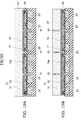
- Figs. 16A and 16B are schematic perspective views of a light emitting device of a second embodiment.
- Figs. 17A and 17B are schematic cross-sectional views of the light emitting device of the second embodiment.
- Fig. 18 is a schematic cross-sectional view of a light emitting module of the second embodiment.
- Figs. 19A to 21B are schematic views showing a method for manufacturing the light emitting device of the second embodiment.
- Figs. 19A to 21B are schematic views showing a method for manufacturing the light emitting device of the second embodiment.
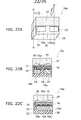
- FIG. 22A to 22C are schematic views of a light emitting device of a third embodiment.
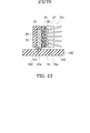
- Fig. 23 is a schematic cross-sectional view of a light emitting module of the third embodiment.
- Figs. 24A to 29B are schematic views showing a method for manufacturing the light emitting device of the third embodiment.
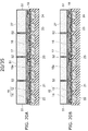
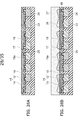
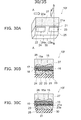
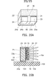
- Figs. 30A to 30C are schematic views of a light emitting device of a fourth embodiment.
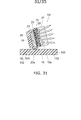
- Fig. 31 is a schematic cross-sectional view of a light emitting module of the fourth embodiment.
- Figs. 32A to 33B are schematic views showing a method for manufacturing the light emitting device of the fourth embodiment.
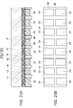
- Fig. 34A is a schematic view of an illumination apparatus in which a light emitting module of a comparative example is used, and Fig.
- Fig. 35A is a schematic view of a light emitting device of a fifth embodiment
- Fig. 35B is a schematic cross-sectional view of a light emitting module of the fifth embodiment.
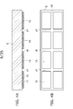
- FIG. 1A is a schematic perspective view of a light emitting device 10a of a first embodiment.
- FIG. 1B is an A-A cross-sectional view of FIG. 1A.
- FIG. 1C is a B-B cross-sectional view of FIG. 1A.
- the light emitting device 10a includes the semiconductor layer 15.
- the semiconductor layer 15 includes a first surface 15a and a second surface opposite to the first surface 15a. Electrodes and interconnect layers are provided on the second surface side. Light is emitted to the outside mainly from the first surface 15a opposite to the second surface.
- the semiconductor layer 15 includes a first semiconductor layer 11 and a second semiconductor layer 12. Both the first semiconductor layer 11 and the second semiconductor layer 12 include, for example, a nitride semiconductor.
- the first semiconductor layer 11 includes, for example, a foundation buffer layer, an n-type layer, etc..
- the n-type layer functions as a lateral-direction path of current.
- the second semiconductor layer 12 includes a stacked structure in which a light emitting layer (an active layer) 13 is interposed between the n-type layer and a p-type layer.
- the second surface side of the semiconductor layer 15 is patterned into an uneven configuration.
- the protrusion formed on the second surface side includes the light emitting layer 13.
- a p-side electrode 16 is provided on the top surface of the second semiconductor layer 12 which is the top surface of the protrusion.
- the p-side electrode 16 is provided in the region including the light emitting layer 13.
- a region where there is no second semiconductor layer 12 is provided on the second surface side of the semiconductor layer 15 beside the protrusion, and an n-side electrode 17 is provided on the top surface of the first semiconductor layer 11 of the region.
- the n-side electrode 17 is provided in a region not including the light emitting layer 13.
- the surface area of the second semiconductor layer 12 including the light emitting layer 13 is greater than the surface area of the first semiconductor layer 11 not including the light emitting layer 13.
- the p-side electrode 16 provided in the region including the light emitting layer 13 has a surface area greater than that of the n-side electrode 17 not including the light emitting layer 13. Thereby, a wide light emitting region is obtained.
- the layout of the p-side electrode 16 and the n-side electrode 17 illustrated in FIG. 6B is one example and is not limited thereto.
- a first insulating layer (hereinbelow referred to as simply the insulating layer) 18 is provided on the second surface side of the semiconductor layer 15.
- the insulating layer 18 covers the semiconductor layer 15, the p-side electrode 16, and the n-side electrode 17.
- another insulating film e.g., a silicon oxide film
- the insulating layer 18 is, for example, a resin such as polyimide having excellent patternability for ultra-fine openings.
- an inorganic substance such as silicon oxide, silicon nitride, etc., may be used as the insulating layer 18.
- the insulating layer 18 includes an interconnect surface 18c on the side opposite to the semiconductor layer 15.
- a p-side metal plate layer 21 and an n-side metal plate layer 22 are provided separately from each other on the interconnect surface 18c.
- the p-side metal plate layer 21 is provided also inside a first via 18a made in the insulating layer 18 to reach the p-side electrode 16 and is electrically connected to the p-side electrode 16. It is not always necessary for the p-side metal plate layer 21 to be formed on the insulating layer 18. For example, a structure may be used in which the p-side metal plate layer 21 is provided only on the p-side electrode 16.
- the n-side metal plate layer 22 is provided also inside a second via 18b made in the insulating layer 18 to reach the n-side electrode 17 and is electrically connected to the n-side electrode 17.
- a p-side metal pillar 23 is provided on the surface of the p-side metal plate layer 21 on the side opposite to the p-side electrode 16.
- the p-side metal plate layer 21 and the p-side metal pillar 23 are included in the p-side interconnect layer of the embodiment.
- An n-side metal pillar 24 is provided on the surface of the n-side metal plate layer 22 on the side opposite to the n-side electrode 17.
- the n-side metal plate layer 22 and the n-side metal pillar 24 are included in the n-side interconnect layer of the embodiment.
- a resin layer 25 is provided as the second insulating layer on the interconnect surface 18c of the insulating layer 18.
- the resin layer 25 covers the p-side metal plate layer 21 and the n-side metal plate layer 22. However, as illustrated in FIG. 1A, a side surface 21a of the p-side metal plate layer 21 and a side surface 22a of the n-side metal plate layer 22 are exposed without being covered with the resin layer 25.
- the resin layer 25 covers the end surface of the p-side metal pillar 23 on the side opposite to the p-side metal plate layer 21 and the end surface of the n-side metal pillar 24 on the side opposite to the n-side metal plate layer 22. Further, the resin layer 25 covers a portion of the side surface of the p-side metal pillar 23 and a portion of the side surface of the n-side metal pillar 24.
- a side surface of a portion of the p-side metal pillar 23 is exposed from the resin layer 25 at a third surface 30 having a plane orientation different from those of the first surface 15a and the second surface of the semiconductor layer 15.
- the exposed surface functions as a p-side external terminal 23a for mounting to the external mounting substrate.
- the third surface 30 is a surface substantially perpendicular to the first surface 15a and the second surface.
- the resin layer 25 has, for example, four side surfaces which have rectangular configurations. One of the side surfaces having a relatively long side is the third surface 30.
- a side surface of a portion of the n-side metal pillar 24 is exposed from the resin layer 25 at the third surface 30.
- the exposed surface functions as an n-side external terminal 24a for mounting to the external mounting substrate.
- the side surface 21a of the p-side metal plate layer 21 also is exposed from the resin layer 25 at the third surface 30 and functions as the p-side external terminal.
- the side surface 22a of the n-side metal plate layer 22 also is exposed from the resin layer 25 at the third surface 30 and functions as the n-side external terminal.
- the portion of the p-side metal pillar 23 other than the p-side external terminal 23a exposed at the third surface 30 is covered with the resin layer 25.
- the portion of the n-side metal pillar 24 other than the n-side external terminal 24a exposed at the third surface 30 is covered with the resin layer 25.
- the structure of the embodiment is one example; and portions of the p-side metal pillar 23 and the n-side metal pillar 24 may be exposed somewhere other than the third surface 30.
- the portion of the p-side metal plate layer 21 other than the side surface 21a exposed at the third surface 30 is covered with the resin layer 25.
- the portion of the n-side metal plate layer 22 other than the side surface 22a exposed at the third surface 30 is covered with the resin layer 25.
- the structure of the embodiment is one example; and portions of the p-side metal plate layer 21 and the n-side metal plate layer 22 may be exposed somewhere other than the third surface 30.
- the distance between the side surface 21a of the p-side metal plate layer 21 exposed at the third surface 30 and the side surface 22a of the n-side metal plate layer 22 exposed at the third surface 30 is greater than the distance between the p-side metal plate layer 21 and the n-side metal plate layer 22 (referring to FIG. 8B) on the interconnect surface 18c of the insulating layer 18.
- the surface area of the p-side metal plate layer 21 can be enlarged.
- the planar size of the p-side metal plate layer 21 is greater than the planar size of the p-side metal pillar 23.
- the p-side metal plate layer 21 can be formed using a low-resistance metal such as, for example, copper. Therefore, it is possible to supply current to the second semiconductor layer 12 with a more uniform distribution as the surface area of the p-side metal plate layer 21 increases. Further, the thermal conductivity of the p-side metal plate layer 21 also can be increased. And it is possible also to efficiently release the heat of the second semiconductor layer 12.
- the p-side electrode 16 spreads to the region which includes the light emitting layer 13. Accordingly, by connecting the p-side metal plate layer 21 and the p-side electrode 16 via the multiple first vias 18a, the current distribution to the light emitting layer 13 can be improved and the heat dissipation of the heat of the light emitting layer 13 also can be improved.
- the side surface 21a of the p-side metal plate layer 21 exposed at the third surface 30 and the side surface 22a of the n-side metal plate layer 22 exposed at the third surface 30 are separated by a distance such that the side surface 21a and the side surface 22a are not shorted to each other by the bonding material such as solder for mounting to the mounting substrate.
- the contact area between the n-side metal plate layer 22 and the n-side metal pillar 24 is greater than the contact area between the n-side metal plate layer 22 and the n-side electrode 17. Also, a portion of the n-side metal plate layer 22 extends over the interconnect surface 18c of the insulating layer 18 to a position extending under the light emitting layer 13.
- an electrode having a wider draw-out can be formed via the n-side metal plate layer 22 from the n-side electrode 17 provided in the narrow region not including the light emitting layer 13 while obtaining a high light output by the light emitting layer 13 being formed over a wide region.
- the contact area between the p-side metal plate layer 21 and the p-side metal pillar 23 is greater than the contact area between the p-side metal plate layer 21 and the p-side electrode 16.
- the contact area between the p-side metal plate layer 21 and the p-side metal pillar 23 is less than the contact area between the p-side metal plate layer 21 and the p-side electrode 16.
- the first semiconductor layer 11 is electrically connected to the n-side metal pillar 24 via the n-side electrode 17 and the n-side metal plate layer 22.
- the second semiconductor layer 12 including the light emitting layer 13 is electrically connected to the p-side metal pillar 23 via the p-side electrode 16 and the p-side metal plate layer 21.
- the p-side metal pillar 23 is thicker than the p-side metal plate layer 21, and the n-side metal pillar 24 is thicker than the n-side metal plate layer 22. Therefore, the mechanical strength of the light emitting device 10a can be increased by the p-side metal pillar 23, the n-side metal pillar 24, and the resin layer 25 filled between the p-side metal pillar 23 and the n-side metal pillar 24 even without a substrate supporting the semiconductor layer 15.
- Copper, gold, nickel, silver, etc. can be used as the material of the p-side metal plate layer 21, the n-side metal plate layer 22, the p-side metal pillar 23, and the n-side metal pillar 24.
- good thermal conductivity, high migration resistance, and excellent adhesion with the insulating material are obtained.
- the resin layer 25 reinforces the p-side metal pillar 23 and the n-side metal pillar 24. It may be used the resin layer 25 to have a coefficient of thermal expansion near to or the same as that of the mounting substrate. Examples of such a resin layer 25 include an epoxy resin, a silicone resin, a fluorocarbon resin, etc.
- a lens 26 and a phosphor layer 27 are provided on the first surface 15a of the semiconductor layer 15 as a transparent body transparent to the light emitted from the light emitting layer 13.
- the lens 26 is provided on the first surface 15a.
- the phosphor layer 27 is provided to cover the lens 26.
- the planar size of the stacked body including each of the components described above provided on the second surface side of the semiconductor layer 15 is substantially the same as the planar size of the phosphor layer 27.
- the lens 26 and the phosphor layer 27 do not obstruct the mounting onto the mounting substrate of the light emitting device 10a because the lens 26 and the phosphor layer 27 do not protrude on the third surface 30 side.
- the phosphor layer 27 includes a transparent resin and a phosphor dispersed in the transparent resin.
- the phosphor layer 27 is capable of absorbing the light emitted from the light emitting layer 13 and emitting a wavelength-converted light. Therefore, the light emitting device 10a is capable of emitting a mixed light of the light from the light emitting layer 13 and the wavelength-converted light of the phosphor layer 27.
- white or lamp, etc. can be obtained as the mixed color of a blue light from the light emitting layer 13 and a yellow light which is the wavelength-converted light of the phosphor layer 27 in the case where the light emitting layer 13 is a nitride semiconductor and the phosphor is a yellow phosphor configured to emit the yellow light.
- the phosphor layer 27 may have a configuration including multiple types of phosphors (e.g., a red phosphor configured to emit red light and a green phosphor configured to emit green light).
- the light emitted from the light emitting layer 13 is emitted to the outside by traveling through mainly the first semiconductor layer 11, the first surface 15a, the lens 26, and the phosphor layer 27.
- the lens 26 may be provided on the phosphor layer 27.
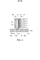
- FIG. 2 is a schematic cross-sectional view of a light emitting module having a configuration in which the light emitting device 10a described above is mounted on a mounting substrate 100.
- the number of the light emitting devices 10a mounted on the mounting substrate 100 is arbitrary and may be singular or multiple. Multiple light emitting devices 10a may be included in a line-shaped light source by being arranged along some one direction.
- the light emitting device 10a is mounted with an attitude in which the third surface 30 is oriented toward a mounting surface 103 of the mounting substrate 100.
- Each of the p-side external terminal 23a and the n-side external terminal 24a exposed at the third surface 30 is bonded with solder 102 to a pad 101 formed on the mounting surface 103.
- An interconnect pattern also is formed on the mounting surface 103 of the mounting substrate 100. The pad 101 is connected to the interconnect pattern.
- the third surface 30 is substantially perpendicular to the first surface 15a which is the main emitting surface of the light. Accordingly, the first surface 15a is oriented not upward from the mounting surface 103 but in the lateral direction with an attitude in which the third surface 30 is oriented downward toward the mounting surface 103 side. In other words, a so-called side-view type light emitting device 10a and light emitting module are obtained in which the light is emitted in the lateral direction in the case where the mounting surface 103 is a horizontal surface.
- the thickness of the p-side metal pillar 23 and the thickness of the n-side metal pillar 24 are thicker than the thickness of the stacked body including the semiconductor layer 15, the p-side electrode 16, the n-side electrode 17, and the insulating layer 18.
- the aspect ratio (the ratio of the thickness to the planar size) of each of the metal pillars 23 and 24 is not limited to being not less than 1; and the ratio thereof may be less than 1. In other words, it is sufficient for the thicknesses of the metal pillars 23 and 24 to be less than the planar sizes thereof.
- the embodiment it is possible to maintain the mechanical strength by the p-side metal pillar 23, the n-side metal pillar 24, and the resin layer 25 being thick even in the case where the semiconductor layer 15 is thin and there is no substrate to support the semiconductor layer 15.
- the stress applied to the semiconductor layer 15 via the solder 102 can be mitigated by being absorbed by the p-side metal pillar 23 and the n-side metal pillar 24.
- a metal or an electrically conductive material other than solder may be used.
- FIG. 3A to FIG. 14B A method for manufacturing the light emitting device 10a of the embodiment will now be described with reference to FIG. 3A to FIG. 14B.
- FIG. 3A to FIG. 14B A method for manufacturing the light emitting device 10a of the embodiment will now be described with reference to FIG. 3A to FIG. 14B.
- FIG. 3A to FIG. 14B A method for manufacturing the light emitting device 10a of the embodiment will now be described with reference to FIG. 3A to FIG. 14B.
- FIG. 3A to FIG. 14B A method for manufacturing the light emitting device 10a of the embodiment will now be described with reference to FIG. 3A to FIG. 14B.
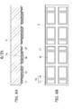
- FIG. 3A illustrates a stacked body of the first semiconductor layer 11 and the second semiconductor layer 12 formed on a major surface of a substrate 5.
- FIG. 3B corresponds to a bottom view of FIG. 3A.
- the first semiconductor layer 11 is formed on the major surface of the substrate 5.
- the second semiconductor layer 12 including the light emitting layer 13 is formed on the first semiconductor layer 11.
- crystal growth of these may be performed by, for example, MOCVD (metal organic chemical vapor deposition) on a sapphire substrate.
- the first semiconductor layer 11 includes a foundation buffer layer and an n-type GaN layer.
- the second semiconductor layer 12 includes the light emitting layer (the active layer) 13 and a p-type GaN layer.
- the light emitting layer 13 may be configured to emit blue, violet, bluish-violet, and ultraviolet light, etc.
- the surface of the first semiconductor layer 11 contacting the substrate 5 is the first surface 15a of the semiconductor layer 15.
- the surface of the second semiconductor layer 12 is a second surface 15b of the semiconductor layer 15.
- a trench is formed in dicing regions d1 and d2 as illustrated in FIG. 4A and FIG. 4B which is the bottom view of FIG. 4A by RIE (Reactive Ion Etching) using a not-illustrated resist.
- the trench is punched through the semiconductor layer 15 and reaches the substrate 5.
- the dicing regions d1 and d2 are formed, for example, in a lattice configuration on the substrate 5 in the wafer state.
- the trench in the dicing regions d1 and d2 also is formed in a lattice configuration to separate the semiconductor layer 15 into multiple chips.
- the process of separating the semiconductor layer 15 into a plurality may be performed after a selective removal of the second semiconductor layer 12 described below or after forming the electrodes.
- FIG. 5A and FIG. 5B which is the bottom view of FIG. 5A by RIE using a not-illustrated resist.
- the region where the first semiconductor layer 11 is exposed does not include the light emitting layer 13.
- the p-side electrode 16 and the n-side electrode 17 are formed on the second surface.
- the p-side electrode 16 is formed on the surface of the second semiconductor layer 12.
- the n-side electrode 17 is formed on the exposed surface of the first semiconductor layer 11.
- the p-side electrode 16 and the n-side electrode 17 may be formed by, for example, sputtering, vapor deposition, etc. Either the p-side electrode 16 or the n-side electrode 17 may be formed first; or the p-side electrode 16 and the n-side electrode 17 may be formed simultaneously from the same material.
- the p-side electrode 16 includes, for example, silver, silver alloy, aluminum, aluminum alloy, etc., that are reflective with respect to the light emitted from the light emitting layer 13. Also, a configuration including a metal protective film to prevent the sulfidization and the oxidization of the p-side electrode 16 may be used.
- a silicon nitride film and/or a silicon oxide film may be formed by CVD (chemical vapor deposition) as a passivation film between the p-side electrode 16 and the n-side electrode 17 and on the end surface (the side surface) of the light emitting layer 13. Activation annealing, etc., to provide an ohmic contact between the semiconductor layer and the electrodes may be implemented if necessary.
- CVD chemical vapor deposition
- the first via 18a and the second via 18b are made selectively in the insulating layer 18 by patterning the insulating layer 18 using, for example, wet etching.
- the first via 18a reaches the p-side electrode 16.
- the second via 18b reaches the n-side electrode 17.
- An organic material for example, such as photosensitive polyimide, benzocyclobutene, etc., may be used as the insulating layer 18. In such a case, it is possible to directly expose and develop the insulating layer 18 without using a resist.
- an inorganic film such as a silicon nitride film, a silicon oxide film, etc., may be used as the insulating layer 18. In the case of the inorganic film, the desired configuration is obtained by etching after the resist is patterned.
- a seed metal 19 is formed on the interconnect surface 18c of the insulating layer 18 which is the surface on the side opposite to the semiconductor layer 15.
- the seed metal 19 may be formed also on the inner wall and the bottom portion of the first via 18a and the inner wall and the bottom portion of the second via 18b.
- the seed metal 19 may be formed using, for example, sputtering.
- the seed metal 19 includes, for example, a stacked film of titanium (Ti) and copper (Cu) stacked in order from the insulating layer 18 side.
- a resist 41 is formed selectively on the seed metal 19; and Cu electroplating is performed using the seed metal 19 as a current path.
- the p-side metal plate layer 21 and the n-side metal plate layer 22 are formed selectively on the interconnect surface 18c of the insulating layer 18.
- the p-side metal plate layer 21 and the n-side metal plate layer 22 are made of, for example, a copper material formed simultaneously by plating.
- the p-side metal plate layer 21 is formed also inside the first via 18a and is electrically connected to the p-side electrode 16 via the seed metal 19.
- the n-side metal plate layer 22 is formed also inside the second via 18b and is electrically connected to the n-side electrode 17 via the seed metal 19.
- the dicing region d2 extends in a direction (the lateral direction of FIG. 8B) along the side surface 21a of the p-side metal plate layer 21 and the side surface 22a of the n-side metal plate layer 22 exposed at the third surface described above. Also, the side surface 21a and the side surface 22a jut onto the dicing region d2.
- Single dot-dash lines e1 and e2 of FIG. 8B illustrate two edges of a dicing blade respectively.
- a notch 21b is made in a portion of the p-side metal plate layer 21 which is on the n-side metal plate layer 22 side and on the side surface 21a side.
- the notch 21b exists between the side surface 21a and the side surface 22a. Therefore, the separation distance between the side surface 21a and the side surface 22a exposed to the outside after the dicing can be a distance sufficient to avoid shorts due to the solder, etc., when mounting.
- the p-side metal plate layer 21 can be proximal to the n-side metal plate layer 22 up to the process limitations; and the surface area of the p-side metal plate layer 21 can be wide.
- the p-side metal plate layer 21 and the p-side electrode 16 can be connected through multiple first vias 18a; and the current distribution and the heat dissipation can be improved.
- the side surface 21a and the side surface 22a exist on both width-direction sides of the dicing region d2 without existing with a bias toward one width-direction side of the dicing region d2.
- the side surface 21a and the side surface 22a which are each metal do not exist with a bias toward the side of one width direction-edge of the dicing blade. Therefore, the occurrence of clogging, damage, etc., due to an excessive load on one width direction-edge of the dicing blade during the dicing can be suppressed.
- the side surface 21a and the side surface 22a that exist on the edge e1 side and the side surface 21a and the side surface 22a that exist on the edge e2 side are arranged alternately as viewed in the direction in which the dicing region d2 extends in FIG. 8B, this is not limited to such a layout. It is sufficient for the side surface 21a and the side surface 22a not to exist with a bias toward the side of one selected from the edge e1 and the edge e2.
- the resist 41 used for the plating of the p-side metal plate layer 21 and the n-side metal plate layer 22 is removed using a solvent or oxygen plasma (FIG. 9A).
- a resist 42 for forming the metal pillars is formed.
- the resist 42 is thicker than the resist 41 described above.
- the resist 41 of the previous processes may remain without being removed; and the resist 42 may be formed to overlap the resist 41.
- FIG. 10A and FIG. 10B which is the bottom view of FIG. 10A, the p-side metal pillar 23 and the n-side metal pillar 24 are formed.
- the p-side metal pillar 23 is formed inside an opening 42a made in the resist 42 and on the surface of the p-side metal plate layer 21.
- the n-side metal pillar 24 is formed inside an opening 42b made in the resist 42 and on the surface of the n-side metal plate layer 22.
- the p-side metal pillar 23 and the n-side metal pillar 24 are made of, for example, a copper material formed simultaneously by plating.
- the single dot-dash lines e1 and e2 of FIG. 10B illustrate two edges of the dicing blade respectively.
- the p-side external terminal 23a and the n-side external terminal 24a exist on both width-direction sides of the dicing region d2 without existing with a bias toward one width-direction side of the dicing region d2.
- the p-side external terminal 23a and the n-side external terminal 24a which are each metal exist without a bias toward the side of one width direction-edge of the dicing blade. Therefore, the occurrence of clogging, damage, etc., due to an excessive load on one width direction-edge of the dicing blade during the dicing can be suppressed.
- the p-side external terminal 23a and the n-side external terminal 24a that exist on the edge e1 side and the p-side external terminal 23a and the n-side external terminal 24a that exist on the edge e2 side are arranged alternately as viewed in the direction in which the dicing region d2 extends in FIG. 10B, this is not limited to such a layout. It is sufficient for the p-side external terminal 23a and the n-side external terminal 24a not to exist with a bias toward the side of one selected from the edge e1 and the edge e2.
- the resist 42 is removed using, for example, a solvent or oxygen plasma (FIG. 11A).
- the exposed portion of the seed metal 19 is removed by wet etching using the p-side metal pillar 23, the n-side metal pillar 24, and a portion of the p-side metal plate layer 21 jutting from the p-side metal pillar 23 as a mask.
- FIG. 11B the electrical connection between the p-side metal plate layer 21 and the n-side metal plate layer 22 via the seed metal 19 is divided.
- the resin layer 25 is stacked on the insulating layer 18.
- the resin layer 25 covers the p-side metal plate layer 21, the n-side metal plate layer 22, the p-side metal pillar 23, and the n-side metal pillar 24.
- the resin layer 25 is insulative. Further, the resin layer 25 may contain, for example, carbon black to make it light-shielding with respect to the light emitted from the light emitting layer. Also, the resin layer 25 may contain a powder that is reflective with respect to the light emitted from the light emitting layer.
- the substrate 5 is removed.
- the substrate 5 may be removed using, for example, laser lift-off.
- laser light is irradiated from the back surface side of the substrate 5 toward the first semiconductor layer 11.
- the laser light has a wavelength that is transmissive with respect to the substrate 5 and in the absorption region of the first semiconductor layer 11.
- the first semiconductor layer 11 proximal to the interface decomposes by absorbing the energy of the laser light.
- the first semiconductor layer 11 is GaN
- the first semiconductor layer 11 decomposes into gallium (Ga) and nitrogen gas.
- the irradiation of the laser light is performed over the entire wafer by performing multiply for every set region; and the substrate 5 is removed.
- the stacked body described above formed on the major surface of the substrate 5 is reinforced by the thick resin layer 25, it is possible to maintain the wafer state even in the case where there is no substrate 5. Also, the resin layer 25 and the metal included in the metal plate layers and the metal pillars are materials softer than the semiconductor layer 15. Therefore, destruction of the device can be avoided even in the case where the large internal stress generated in the epitaxial process that forms the semiconductor layer 15 on the substrate 5 is released all at once when peeling the substrate 5.
- the first surface 15a of the semiconductor layer 15 from which the substrate 5 is removed is cleaned.
- the gallium (Ga) adhered to the first surface 15a is removed using, for example, hydrochloric acid, etc.
- the first surface 15a is etched using, for example, a KOH (potassium hydroxide) aqueous solution, TMAH (tetramethylammonium hydroxide), etc.
- a KOH potassium hydroxide
- TMAH tetramethylammonium hydroxide
- an unevenness is formed in the first surface 15a due to the difference of the etching rates that depend on the crystal plane orientation (FIG. 13A).
- the unevenness may be formed in the first surface 15a by performing the etching after the patterning using the resist. The light extraction efficiency can be increased by the unevenness being formed in the first surface 15a.
- the lens 26 is formed on the first surface 15a.
- the lens 26 is transparent to the emitted light from the light emitting layer; and, for example, a silicone resin, an acrylic resin, glass, etc., may be used.
- the lens 26 can be formed by, for example, etching using a grayscale mask and/or imprinting.
- the phosphor layer 27 is formed on the first surface 15a and on the insulating layer 18 exposed between the mutually-adjacent semiconductor layer 15 to cover the lens 26.
- a liquid transparent resin having dispersed phosphor particles is supplied using a method such as printing, potting, molding, compression molding, etc., and is subsequently thermally cured.
- the transparent resin is transmissive to the light emitted from the light emitting layer and the light emitted by the phosphor; and, for example, a material such as a silicone resin, an acrylic resin, liquid glass, etc., may be used.
- the phosphor layer 27, the insulating layer 18, and the resin layer 25 are cut at the positions where the dicing regions d1 and d2 are formed in the lattice configuration to singulate into the multiple light emitting devices 10a.
- the cutting is performed using a dicing blade.
- the cutting may be performed using laser irradiation.
- the portions of the p-side metal pillar 23 and the n-side metal pillar 24 jutting into the dicing region d2 extending in the direction along the third surface 30 are cut. Thereby, the p-side external terminal 23a and the n-side external terminal 24a are exposed at the third surface 30.
- the portions of the p-side metal plate layer 21 and the n-side metal plate layer 22 jutting into the dicing region d2 are cut (FIG. 8B). Thereby, the side surface 21a of the p-side metal plate layer 21 and the side surface 22a of the n-side metal plate layer 22 also are exposed at the third surface 30.
- the substrate 5 When dicing, the substrate 5 is already removed. Further, damage to the semiconductor layer 15 during the dicing can be avoided because the semiconductor layer 15 does not exist in the dicing regions d1 and d2. Also, a structure is obtained in which the end portion (the side surface) of the semiconductor layer 15 is protected by being covered with the resin after the singulation.
- the singulated light emitting device 10a may have a single-chip structure including one semiconductor layer 15 or a multi-chip structure including multiple semiconductor layers 15.
- a structure may be used in which a lens is not provided on the first surface 15a side as in a light emitting device 10b illustrated in FIG. 15A.
- the substrate 5 may thinly remain on the first surface 15a as in a light emitting device 10c illustrated in FIG. 15B.
- the substrate 5 can be polished using a grinder for polishing a semiconductor wafer back surface, etc.
- the substrate 5 is, for example, a sapphire substrate and is transmissive to the light emitted from the nitride semiconductor-type light emitting layer. In such a case, because there is no phosphor layer, light having the same wavelength as the emitted light from the light emitting layer is emitted to the outside from the light emitting device 10c. Of course, a phosphor layer may be formed on the substrate 5.
- the mechanical strength can be increased and a structure having high reliability is possible by leaving the substrate 5.
- a half-cut can be made using a dicing blade from the resin layer 25 side; and subsequently, the substrate 5 can be subdivided using laser irradiation. Alternatively, all portions may be cut using laser irradiation.
- FIG. 16A is a schematic perspective view as viewed from the third surface 30 side of a light emitting device 10d of a second embodiment.
- FIG. 16B is a schematic perspective view as viewed from the light emitting surface side of the light emitting device 10d.
- FIG. 17A is an A-A cross-sectional view of FIG. 16A.
- FIG. 17B is a B-B cross-sectional view of FIG. 16A.
- the light emitting device 10d of the embodiment is different from the light emitting device 10a of the first embodiment in that a reflective film 51 is included.
- the reflective film 51 is reflective with respect to the light emitted from the light emitting layer and the light emitted by the phosphor.
- the reflective film 51 is, for example, a metal film.
- the reflective film 51 is formed on the side surface of the phosphor layer 27 and the side surface of the insulating layer 18.
- the reflective film 51 is not formed on the surface of the phosphor layer 27 on the side opposite to the first surface 15a.
- FIG. 18 is a schematic cross-sectional view of a light emitting module having a configuration in which the light emitting device 10d of the embodiment is mounted on the mounting substrate 100.
- the light emitting device 10d is mounted with an attitude in which the third surface 30 is oriented toward the mounting surface 103 of the mounting substrate 100.
- Each of the p-side external terminal 23a and the n-side external terminal 24a exposed at the third surface 30 is bonded with the solder 102, etc., to the pad 101 formed in the mounting surface 103.
- the third surface 30 is substantially perpendicular to the first surface 15a which is the main emitting surface of the light. Accordingly, the first surface 15a is oriented not upward from the mounting surface 103 but in the lateral direction with an attitude in which the third surface 30 is oriented downward toward the mounting surface 103 side. In other words, a so-called side-view type light emitting device 10d and light emitting module are obtained in which the light is emitted in the lateral direction in the case where the mounting surface 103 is a horizontal surface.
- the light is emitted by being concentrated in the lateral direction.
- FIG. 19A illustrates the state in which the substrate 5 is removed and the phosphor layer 27 is formed on the first surface 15a. Up to this process, the processes progress similarly to those of the first embodiment described above.
- half-cut dicing is performed on the stacked body illustrated in FIG. 19A from the phosphor layer 27 side. Specifically, the phosphor layer 27 and the insulating layer 18 are cut at the positions of the dicing regions d1 and d2. For example, the cutting is performed using a dicing blade or laser irradiation. Thereby, a trench 52 (FIG. 19B) is made in the dicing regions d1 and d2.
- the reflective film 51 is formed by, for example, performing sputtering onto the exposed surface. As illustrated in FIG. 20A, the reflective film 51 is formed on the upper surface of the phosphor layer 27 and the bottom portion and the inner wall of the trench 52.
- the reflective film 51 can be used as the reflective film 51.
- a resin including a reflective powder may be used as the reflective film 51.
- the reflective film 51 formed on the upper surface of the phosphor layer 27 is removed by polishing.
- a grinder for polishing a semiconductor wafer back surface, etc. can be used.
- the reflective film 51 formed on the upper surface of the phosphor layer 27 may be removed using RIE.
- the reflective film 51 remains on the side surface of the phosphor layer 27 and the side surface of the insulating layer 18.
- the resin layer 25 under the trench 52 is cut (FIGS. 21A and 21B).
- the cutting is performed using, for example, a dicing blade.
- the cutting may be performed using laser irradiation. Thereby, singulation is performed into the multiple light emitting devices 10d.
- the portions of the p-side metal pillar 23 and the n-side metal pillar 24 jutting into the dicing region d2 extending in the direction along the third surface 30 are cut. Thereby, the p-side external terminal 23a and the n-side external terminal 24a are exposed at the third surface 30.
- the dicing can be easy and the productivity can be increased because the resin is cut. Further, because the semiconductor layer 15 is not cut, the damage to the semiconductor layer 15 during the dicing can be avoided.
- FIG. 22A is a schematic perspective view of a light emitting device 10e of a third embodiment.
- FIG. 22B is an A-A cross-sectional view of FIG. 22A.
- FIG. 22C is a B-B cross-sectional view of FIG. 22A.
- a portion of the p-side metal pillar 23 is provided inside the first via 18a without the p-side metal plate layer being provided. Further, a portion of the n-side metal pillar 24 is provided inside the second via 18b without the n-side metal plate layer being provided.
- FIG. 23 is a schematic cross-sectional view of a light emitting module having a configuration in which the light emitting device 10e of the embodiment is mounted on the mounting substrate 100.
- the light emitting device 10e is mounted with an attitude in which the third surface 30 is oriented toward the mounting surface 103 of the mounting substrate 100. Then, each of the p-side external terminal 23a and the n-side external terminal 24a exposed at the third surface 30 is bonded with the solder 102, etc., to the pad 101 formed in the mounting surface 103.
- the third surface 30 is substantially perpendicular to the first surface 15a which is the main emitting surface of the light. Accordingly, the first surface 15a is oriented not upward from the mounting surface 103 but in the lateral direction with an attitude in which the third surface 30 is oriented downward toward the mounting surface 103 side. In other words, a so-called side-view type light emitting device 10e and light emitting module are obtained in which the light is emitted in the lateral direction in the case where the mounting surface 103 is a horizontal surface.
- the resist 42 is formed selectively on the seed metal 19; and Cu electroplating is performed using the seed metal 19 as a current path.
- FIG. 25A and FIG. 25B which is the bottom view of FIG. 25A, the p-side metal pillar 23 and the n-side metal pillar 24 are formed on the interconnect surface 18c of the insulating layer 18.
- a portion of the p-side metal pillar 23 is formed also inside the first via 18a and is electrically connected to the p-side electrode 16 via the seed metal 19.
- a portion of the n-side metal pillar 24 is formed also inside the second via 18b and is electrically connected to the n-side electrode 17 via the seed metal 19.
- the resist 42 is removed using, for example, a solvent or oxygen plasma (FIG. 26A).
- the exposed portion of the seed metal 19 is removed by wet etching using the p-side metal pillar 23 and the n-side metal pillar 24 as a mask. Thereby, as illustrated in FIG. 26B, the electrical connection between the p-side metal pillar 23 and the n-side metal pillar 24 via the seed metal 19 is broken.
- the resin layer 25 is stacked on the insulating layer 18.
- the resin layer 25 covers the p-side metal pillar 23 and the n-side metal pillar 24.
- the substrate 5 is removed.
- the substrate 5 is removed using, for example, laser lift-off.
- an unevenness is formed in the first surface 15a by etching the first surface 15a using, for example, a KOH (potassium hydroxide) aqueous solution, TMAH (tetramethylammonium hydroxide), etc. (FIG. 28A).
- KOH potassium hydroxide
- TMAH tetramethylammonium hydroxide
- the lens 26 is formed on the first surface 15a. Further, the phosphor layer 27 is formed on the first surface 15a and on the insulating layer 18 exposed between the mutually-adjacent semiconductor layer 15 to cover the lens 26.
- the phosphor layer 27, the insulating layer 18, and the resin layer 25 are cut at the positions of the dicing regions d1 and d2 formed in the lattice configuration to singulate into the multiple light emitting devices 10e.
- the portions of the p-side metal pillar 23 and the n-side metal pillar 24 jutting into the dicing region d2 extending in the direction along the third surface 30 are cut. Thereby, the p-side external terminal 23a and the n-side external terminal 24a are exposed at the third surface 30.
- FIG. 30A is a schematic perspective view of a light emitting device 10f of a fourth embodiment.
- FIG. 30B is an A-A cross-sectional view of FIG. 30A.
- FIG. 30C is a B-B cross-sectional view of FIG. 30A.
- the third surface 30 of the light emitting device 10f of the embodiment is neither perpendicular nor parallel but is tilted.
- the third surface 30 is tilted such that the exterior form of the resin layer 25 has an inverted trapezoidal configuration.
- the p-side external terminal 23a of the p-side metal pillar 23, the n-side external terminal 24a of the n-side metal pillar 24, the side surface 21a of the p-side metal plate layer 21, and the side surface 22a of the n-side metal plate layer 22 exposed at the third surface 30 also are tilted along the tilt of the third surface 30.
- FIG. 31 is a schematic cross-sectional view of a light emitting module having a configuration in which the light emitting device 10f of the embodiment is mounted on the mounting substrate 100.
- the light emitting device 10f is mounted with an attitude in which the third surface 30 is oriented toward the mounting surface 103 of the mounting substrate 100.
- Each of the p-side external terminal 23a and the n-side external terminal 24a exposed at the third surface 30 is bonded with the solder 102, etc., to the pad 101 formed in the mounting surface 103.
- the p-side external terminal 23a and the n-side external terminal 24a are exposed at the third surface 30 having the plane orientation different from those of the first surface 15a and the second surface opposite to the first surface 15a. Therefore, a side-view type light emitting device 10f and light emitting module are obtained in which light is emitted in the lateral direction in the state in which the mounting surface is downward.
- the third surface 30 is tilted with respect to the first surface 15a, the first surface 15a is oriented obliquely upward with an attitude in which the third surface 30 is oriented downward toward the mounting surface 103 side.
- the light is emitted obliquely upward in the case where the mounting surface 103 is a horizontal surface.
- FIG. 32B corresponds to the A-A cross section of FIG. 32A; and FIG. 33B corresponds to the A-A cross section of FIG. 33A.
- the resin layer 25 is cut at the position of the dicing region d2 illustrated in FIG. 10B described above using a blade of which, for example, both width-direction side surfaces are formed with tapers.
- a trench 55 is made under the dicing region d2.
- the trench 55 reaches the insulating layer 18 by piercing the resin layer 25.
- the trench 55 widens gradually away from the insulating layer 18 side.
- the p-side external terminal 23a and the n-side external terminal 24a jut into the dicing region d2. Accordingly, the p-side external terminal 23a and the n-side external terminal 24a are exposed at the trench 55.
- the insulating layer 18 and the phosphor layer 27 are cut on the trench 55 along the dicing region d2. Further, the phosphor layer 27, the insulating layer 18, and the resin layer 25 are cut along the dicing region d1 orthogonal to the dicing region d2. Thereby, as illustrated in FIGS. 33A and 33B, singulation into the multiple light emitting devices 10f is performed.
- the side surface of the resin layer 25 illustrated in FIG. 33A may be tilted by dicing using a blade of which both width-direction side surfaces are formed with tapers.
- FIG. 35A is a schematic perspective view of the light emitting device of a fifth embodiment.
- FIG. 35B is a schematic cross-sectional view of a light emitting module having a configuration in which the light emitting device is mounted on the mounting substrate 100.
- a surface 23b and a surface 24b which are different from the p-side external terminal 23a of the p-side metal pillar 23 and the n-side external terminal 24a of the n-side metal pillar 24, are exposed in the wafer state.
- the surface 23b and the surface 24b are exposed at the surface 60, which is different from the third surface 30 oriented toward the mounting surface 103 of the mounting substrate 100.
- the surface 60 is a surface on the side opposite to the light emitting surface.
- the light emitting surface corresponds to one surface of the wafer; and the surface 60 corresponds to one other surface. Accordingly, the surface 60 is exposed in the wafer state, which is different from the p-side external terminal 23a and the n-side external terminal 24a which are exposed after the dicing.
- the surfaces 23b and 24b can be utilized as wafer level measurement terminals.
- the light emitting device can emit light and various inspections can be performed.
- the inspection is performed in the wafer level in which handling is easy.
- the surfaces 23b and 24b are covered with an insulating film (e.g., a resin) 71 illustrated in FIG. 35B.
- the formation of the insulating film 71 is performed collectively in the wafer state.
- the singulated light emitting device of the embodiment is mounted with an attitude in which the third surface 30 is oriented toward the mounting surface 103 of the mounting substrate 100.
- Each of the p-side external terminal 23a and the n-side external terminal 24a exposed at the third surface 30 is bonded with the solder 102, etc., to the pad 101 formed in the mounting surface 103.
- the surfaces 23b and 24b described above are covered with the insulating film 71 and are not exposed. Therefore, wetting of the solder up onto the surfaces 23b and 24b can be prevented. As a result, mounting defects such as tilting of the light emitting device and the light emitting surface rising to be oriented upward due to the wetting of the solder can be prevented.
- FIG. 34B is a schematic view of a specific example in which the light emitting module of the embodiment is used as, for example, a backlight of a liquid crystal display apparatus.
- a light emitting device 10 mounted on the mounting substrate 100 is illustrated as one typical light emitting device of the embodiments described above.
- the mounting substrate 100 is provided on a frame 151. Because the light emitting device 10 is the side-view type, the light is emitted in the lateral direction as illustrated by the white arrow of the drawing in the state in which the mounting substrate 100 is downward.
- the mounting substrate 100 is formed with, for example, a rectangular plate configuration extending into the page surface; and the multiple light emitting devices 10 are mounted in the longitudinal direction of the rectangular plate.
- a light guide plate 201 is provided beside the light emitting module.
- the light guide plate 201 is transmissive to the light emitted from the light emitting device 10 and is made of, for example, a resin material.
- the light emitting surface of the light emitting device 10 faces a light incident surface 201a of the light guide plate 201.
- a reflector 153 is provided below the light guide plate 201; and a liquid crystal panel 202 is provided above the light guide plate 201. Also, a reflector 154 is provided above the light emitting device 10. The reflectors 153 and 154 are reflective with respect to the light emitted from the light emitting device 10.
- the light emitted in the lateral direction from the light emitting device 10 is incident on the light incident surface 201a of the light guide plate 201.
- the light incident on the light guide plate 201 from the light incident surface 201a spreads in the surface direction of the light guide plate 201 and is incident on the liquid crystal panel 202.
- the light from the light guide plate 201 that is emitted from the opposite side of the liquid crystal panel 202 is reflected by the reflector 153 and guided into the liquid crystal panel 202.
- FIG. 34A is a schematic view of a backlight in which a light emitting module of a comparative example is used as the light source.
- a light emitting device 300 of the light emitting module of the comparative example is a so-called top-view type.
- the light is emitted upward from the mounting surface of the mounting substrate 100.
- the mounting substrate 100 is supported by a frame 152 provided to oppose the light incident surface 201a to cause the light emitting surface of the light emitting device 300 to oppose the light incident surface 201a of the light guide plate 201.
- the mounting substrate 100 having the rectangular plate configuration is disposed upright with an attitude in which the mounting surface is oriented toward the light incident surface 201a; and this may lead to an increase of not only the thickness of the light guide plate 201 but also the thickness of the entire backlight unit.
- the red phosphor layer, the yellow phosphor layer, the green phosphor layer, and the blue phosphor layer described below can be used as the phosphor layer described above.
- the red phosphor layer can contain, for example, a nitride-based phosphor of CaAlSiN 3 :Eu or a SiAlON-based phosphor.
- (M 1-x , R x ) a1 AlSi b1 O c1 N d1 Compositional Formula (1) can be used (where M is at least one type of metal element excluding Si and Al, and it may be desirable for M to be at least one selected from Ca and Sr; R is a light emission center element, and it may be desirable for R to be Eu; and x, a1, b1, c1, and d1 satisfy the following relationships: x is larger than 0 and 1 or less, a1 is larger than 0.6 and less than 0.95, b1 is larger than 2 and less than 3.9, c1 is larger than 0.25 and less than 0.45, and d1 is larger than 4 and less than 5.7).
- the temperature characteristics of the wavelength conversion efficiency can be improved; and the efficiency in the high current density region can be increased further.
- the yellow phosphor layer can contain, for example, a silicate-based phosphor of (Sr, Ca, Ba) 2 SiO 4 :Eu.
- the green phosphor layer can contain, for example, a halophosphate-based phosphor of (Ba, Ca, Mg) 10 (PO 4 ) 6 Cl 2 :Eu or a SiAlON-based phosphor.
- (M 1-x , R x ) a2 AlSi b2 O c2 N d2 Compositional Formula (2) can be used (where M is at least one type of metal element excluding Si and Al, and it may be desirable for M to be at least one selected from Ca and Sr; R is a light emission center element, and it may be desirable for R to be Eu; and x, a2, b2, c2, and d2 satisfy the following relationships: x is larger than 0 and 1 or less, a2 is larger than 0.93 and less than 1.3, b2 is larger than 4.0 and less than 5.8, c2 is larger than 0.6 and less than 1, and d2 is larger than 6 and less than 11).
- the temperature characteristics of the wavelength conversion efficiency can be improved; and the efficiency in the high current density region can be increased further.
- the blue phosphor layer can contain, for example, an oxide-based phosphor of BaMgAl 10 O 17 :Eu.
Priority Applications (4)
| Application Number | Priority Date | Filing Date | Title |
|---|---|---|---|
| CN201180069018.1A CN103403890B (zh) | 2011-01-14 | 2011-08-10 | 发光器件、发光模块以及用于制造发光器件的方法 |
| EP11760577.4A EP2664013B1 (en) | 2011-01-14 | 2011-08-10 | Light emitting device, light emitting module, and method for manufacturing light emitting device |
| KR1020137018352A KR101427547B1 (ko) | 2011-01-14 | 2011-08-10 | 발광 장치, 발광 모듈 및 발광 장치의 제조 방법 |
| US13/940,754 US8957434B2 (en) | 2011-01-14 | 2013-07-12 | Light emitting device, light emitting module, and method for manufacturing light emitting device |
Applications Claiming Priority (2)
| Application Number | Priority Date | Filing Date | Title |
|---|---|---|---|
| JP2011005625A JP5537446B2 (ja) | 2011-01-14 | 2011-01-14 | 発光装置、発光モジュール、発光装置の製造方法 |
| JP2011-005625 | 2011-01-14 |
Related Child Applications (1)
| Application Number | Title | Priority Date | Filing Date |
|---|---|---|---|
| US13/940,754 Continuation US8957434B2 (en) | 2011-01-14 | 2013-07-12 | Light emitting device, light emitting module, and method for manufacturing light emitting device |
Publications (1)
| Publication Number | Publication Date |
|---|---|
| WO2012095903A1 true WO2012095903A1 (en) | 2012-07-19 |
Family
ID=44674841
Family Applications (1)
| Application Number | Title | Priority Date | Filing Date |
|---|---|---|---|
| PCT/JP2011/004534 WO2012095903A1 (en) | 2011-01-14 | 2011-08-10 | Light emitting device, light emitting module, and method for manufacturing light emitting device |
Country Status (7)
| Country | Link |
|---|---|
| US (1) | US8957434B2 (zh) |
| EP (1) | EP2664013B1 (zh) |
| JP (1) | JP5537446B2 (zh) |
| KR (1) | KR101427547B1 (zh) |
| CN (1) | CN103403890B (zh) |
| TW (1) | TWI529959B (zh) |
| WO (1) | WO2012095903A1 (zh) |
Cited By (2)
| Publication number | Priority date | Publication date | Assignee | Title |
|---|---|---|---|---|
| US9917234B2 (en) | 2015-08-04 | 2018-03-13 | Nichia Corporation | Method of manufacturing light emitting device |
| EP2689475B1 (en) * | 2011-03-25 | 2018-05-02 | Kabushiki Kaisha Toshiba | Light emitting device, light emitting module, and method for manufacturing light emitting device |
Families Citing this family (27)
| Publication number | Priority date | Publication date | Assignee | Title |
|---|---|---|---|---|
| JP5850523B2 (ja) * | 2011-09-22 | 2016-02-03 | シチズン電子株式会社 | Ledチップ |
| WO2014027380A1 (ja) * | 2012-08-14 | 2014-02-20 | ウェーブスクエア,インコーポレイテッド | Iii族窒化物半導体素子およびその製造方法 |
| JP6029912B2 (ja) * | 2012-09-25 | 2016-11-24 | スタンレー電気株式会社 | 半導体発光素子 |
| JP6107024B2 (ja) * | 2012-09-26 | 2017-04-05 | 日亜化学工業株式会社 | 発光装置およびその製造方法 |
| KR101980230B1 (ko) * | 2012-10-09 | 2019-09-02 | 삼성디스플레이 주식회사 | 플렉서블 디스플레이 장치용 어레이 기판과, 이의 제조 방법 |
| JP2014139998A (ja) * | 2013-01-21 | 2014-07-31 | Toshiba Corp | 半導体発光装置 |
| CN105378948B (zh) * | 2013-07-18 | 2020-08-28 | 亮锐控股有限公司 | 切分发光器件的晶片 |
| JP6303344B2 (ja) | 2013-09-05 | 2018-04-04 | 日亜化学工業株式会社 | 発光装置 |
| CN103700662B (zh) * | 2013-12-09 | 2017-02-15 | 京东方科技集团股份有限公司 | 一种承载基板和柔性显示器件制作方法 |
| JP6256026B2 (ja) | 2014-01-17 | 2018-01-10 | 日亜化学工業株式会社 | 発光装置及び発光装置の製造方法 |
| JP6354273B2 (ja) * | 2014-04-10 | 2018-07-11 | 日亜化学工業株式会社 | 発光装置及び発光装置の製造方法 |
| JP6361374B2 (ja) | 2014-08-25 | 2018-07-25 | 日亜化学工業株式会社 | 発光装置及びその製造方法 |
| JP6582382B2 (ja) | 2014-09-26 | 2019-10-02 | 日亜化学工業株式会社 | 発光装置の製造方法 |
| JP6519177B2 (ja) | 2014-12-26 | 2019-05-29 | 日亜化学工業株式会社 | 発光装置及び発光装置の製造方法 |
| CN105990507B (zh) * | 2015-03-18 | 2019-09-17 | 新世纪光电股份有限公司 | 侧照式发光二极管结构及其制造方法 |
| DE102015109755A1 (de) * | 2015-06-18 | 2016-12-22 | Osram Opto Semiconductors Gmbh | Bauelement und Verfahren zur Herstellung eines Bauelements |
| DE102015111492B4 (de) | 2015-07-15 | 2023-02-23 | OSRAM Opto Semiconductors Gesellschaft mit beschränkter Haftung | Bauelemente und Verfahren zur Herstellung von Bauelementen |
| JP2017050350A (ja) * | 2015-08-31 | 2017-03-09 | 日亜化学工業株式会社 | 発光装置及びその製造方法 |
| CN111223975A (zh) | 2015-09-18 | 2020-06-02 | 新世纪光电股份有限公司 | 发光装置及其制造方法 |
| JP6645213B2 (ja) * | 2016-01-27 | 2020-02-14 | オムロン株式会社 | 発光装置、および発光装置の製造方法 |
| TWI651870B (zh) | 2016-10-19 | 2019-02-21 | 新世紀光電股份有限公司 | 發光裝置及其製造方法 |
| CN109037262A (zh) * | 2017-06-09 | 2018-12-18 | 美商晶典有限公司 | 微发光二极管显示模块的制造方法 |
| CN109216513B (zh) * | 2017-06-30 | 2023-05-23 | 日亚化学工业株式会社 | 发光装置及其制造方法 |
| TW201919261A (zh) | 2017-11-05 | 2019-05-16 | 新世紀光電股份有限公司 | 發光裝置 |
| US11158774B2 (en) | 2018-12-14 | 2021-10-26 | Nichia Corporation | Light-emitting device, light-emitting module, and method of manufacturing light-emitting device |
| JP7223938B2 (ja) * | 2019-02-12 | 2023-02-17 | 日亜化学工業株式会社 | 発光装置の製造方法 |
| US11804416B2 (en) * | 2020-09-08 | 2023-10-31 | UTAC Headquarters Pte. Ltd. | Semiconductor device and method of forming protective layer around cavity of semiconductor die |
Citations (3)
| Publication number | Priority date | Publication date | Assignee | Title |
|---|---|---|---|---|
| US20080093607A1 (en) * | 2006-10-23 | 2008-04-24 | Hong Kong Applied Science and Technology Research Institute Company Limited | Light emitting diode device, method of fabrication and use thereof |
| US20080101062A1 (en) * | 2006-10-27 | 2008-05-01 | Hong Kong Applied Science and Technology Research Institute Company Limited | Lighting device for projecting a beam of light |
| EP2197051A2 (en) * | 2008-12-12 | 2010-06-16 | Kabushiki Kaisha Toshiba | Light emitting device and method for manufacturing the same |
Family Cites Families (39)
| Publication number | Priority date | Publication date | Assignee | Title |
|---|---|---|---|---|
| JPH02197051A (ja) | 1989-01-25 | 1990-08-03 | Jeol Ltd | 透過型位相差電子顕微鏡 |
| JP3342322B2 (ja) | 1996-11-27 | 2002-11-05 | シャープ株式会社 | Led素子表示装置の製造方法 |
| JP3337405B2 (ja) * | 1996-12-27 | 2002-10-21 | シャープ株式会社 | 発光表示素子およびその電気配線基板への接続方法ならびに製造方法 |
| JP2000244012A (ja) | 1998-12-22 | 2000-09-08 | Toyoda Gosei Co Ltd | Iii族窒化物系化合物半導体素子の製造方法 |
| JP3589187B2 (ja) | 2000-07-31 | 2004-11-17 | 日亜化学工業株式会社 | 発光装置の形成方法 |
| JP2002057274A (ja) * | 2000-08-09 | 2002-02-22 | Matsushita Electric Ind Co Ltd | 光高周波回路 |
| JP2004311480A (ja) * | 2003-04-02 | 2004-11-04 | Matsushita Electric Works Ltd | 半導体発光素子 |
| JP4305102B2 (ja) | 2003-09-03 | 2009-07-29 | 豊田合成株式会社 | 半導体発光素子用複合基板及びその製造方法、並びに半導体発光素子の製造方法 |
| JP2005079551A (ja) | 2003-09-03 | 2005-03-24 | Toyoda Gosei Co Ltd | 半導体発光素子形成用複合基板及びその製造方法、並びに半導体発光素子の製造方法。 |
| US7847411B2 (en) * | 2003-11-07 | 2010-12-07 | Shinko Electric Industries Co., Ltd. | Electronic device and method of manufacturing the same |
| JP4121536B2 (ja) | 2004-09-27 | 2008-07-23 | 松下電器産業株式会社 | 半導体発光素子、その製造方法及びその実装方法、並びに発光装置 |
| JP2006128625A (ja) | 2004-09-30 | 2006-05-18 | Oki Electric Ind Co Ltd | 半導体装置及びその製造方法 |
| JP5329787B2 (ja) * | 2007-09-28 | 2013-10-30 | パナソニック株式会社 | 実装基板およびledモジュール |
| JP2009177117A (ja) * | 2007-12-25 | 2009-08-06 | Toshiba Lighting & Technology Corp | 表示装置 |
| JP5495495B2 (ja) * | 2008-02-18 | 2014-05-21 | シチズン電子株式会社 | 表面実装型発光ダイオード |
| JP4799606B2 (ja) * | 2008-12-08 | 2011-10-26 | 株式会社東芝 | 光半導体装置及び光半導体装置の製造方法 |
| JP4686625B2 (ja) | 2009-08-03 | 2011-05-25 | 株式会社東芝 | 半導体発光装置の製造方法 |
| JP2011071272A (ja) | 2009-09-25 | 2011-04-07 | Toshiba Corp | 半導体発光装置及びその製造方法 |
| JP5378130B2 (ja) | 2009-09-25 | 2013-12-25 | 株式会社東芝 | 半導体発光装置 |
| JP5534763B2 (ja) | 2009-09-25 | 2014-07-02 | 株式会社東芝 | 半導体発光装置の製造方法及び半導体発光装置 |
| JP5349260B2 (ja) | 2009-11-19 | 2013-11-20 | 株式会社東芝 | 半導体発光装置及びその製造方法 |
| JP5414579B2 (ja) | 2009-11-19 | 2014-02-12 | 株式会社東芝 | 半導体発光装置 |
| JP5101645B2 (ja) | 2010-02-24 | 2012-12-19 | 株式会社東芝 | 半導体発光装置 |
| JP5197654B2 (ja) | 2010-03-09 | 2013-05-15 | 株式会社東芝 | 半導体発光装置及びその製造方法 |
| JP5202559B2 (ja) | 2010-03-09 | 2013-06-05 | 株式会社東芝 | 半導体発光装置及びその製造方法 |
| JP2011199193A (ja) | 2010-03-23 | 2011-10-06 | Toshiba Corp | 発光装置及びその製造方法 |
| JP5101650B2 (ja) | 2010-03-25 | 2012-12-19 | 株式会社東芝 | 半導体発光装置及びその製造方法 |
| JP5356312B2 (ja) | 2010-05-24 | 2013-12-04 | 株式会社東芝 | 半導体発光装置 |
| JP5325834B2 (ja) | 2010-05-24 | 2013-10-23 | 株式会社東芝 | 半導体発光装置及びその製造方法 |
| JP5281612B2 (ja) | 2010-05-26 | 2013-09-04 | 株式会社東芝 | 半導体発光装置及びその製造方法 |
| JP5426481B2 (ja) | 2010-05-26 | 2014-02-26 | 株式会社東芝 | 発光装置 |
| JP2011253925A (ja) | 2010-06-02 | 2011-12-15 | Toshiba Corp | 発光装置の製造方法 |
| JP5390472B2 (ja) | 2010-06-03 | 2014-01-15 | 株式会社東芝 | 半導体発光装置及びその製造方法 |
| TW201145614A (en) | 2010-06-03 | 2011-12-16 | Toshiba Kk | Method for manufacturing light-emitting device and light-emitting device manufactured by the same |
| JP2011253975A (ja) | 2010-06-03 | 2011-12-15 | Toshiba Corp | 発光装置およびその製造方法 |
| JP5337105B2 (ja) | 2010-06-03 | 2013-11-06 | 株式会社東芝 | 半導体発光装置 |
| US20110298001A1 (en) | 2010-06-03 | 2011-12-08 | Kabushiki Kaisha Toshiba | Method for manufacturing light-emitting device and light-emitting device manufactured by the same |
| JP5337106B2 (ja) | 2010-06-04 | 2013-11-06 | 株式会社東芝 | 半導体発光装置 |
| JP5657591B2 (ja) * | 2011-03-23 | 2015-01-21 | 株式会社東芝 | 半導体発光装置およびその製造方法 |
-
2011
- 2011-01-14 JP JP2011005625A patent/JP5537446B2/ja active Active
- 2011-08-10 KR KR1020137018352A patent/KR101427547B1/ko active IP Right Grant
- 2011-08-10 CN CN201180069018.1A patent/CN103403890B/zh active Active
- 2011-08-10 EP EP11760577.4A patent/EP2664013B1/en active Active
- 2011-08-10 WO PCT/JP2011/004534 patent/WO2012095903A1/en active Application Filing
- 2011-09-16 TW TW100133436A patent/TWI529959B/zh active
-
2013
- 2013-07-12 US US13/940,754 patent/US8957434B2/en active Active
Patent Citations (4)
| Publication number | Priority date | Publication date | Assignee | Title |
|---|---|---|---|---|
| US20080093607A1 (en) * | 2006-10-23 | 2008-04-24 | Hong Kong Applied Science and Technology Research Institute Company Limited | Light emitting diode device, method of fabrication and use thereof |
| US20080101062A1 (en) * | 2006-10-27 | 2008-05-01 | Hong Kong Applied Science and Technology Research Institute Company Limited | Lighting device for projecting a beam of light |
| EP2197051A2 (en) * | 2008-12-12 | 2010-06-16 | Kabushiki Kaisha Toshiba | Light emitting device and method for manufacturing the same |
| JP2010141176A (ja) | 2008-12-12 | 2010-06-24 | Toshiba Corp | 発光装置及びその製造方法 |
Cited By (4)
| Publication number | Priority date | Publication date | Assignee | Title |
|---|---|---|---|---|
| EP2689475B1 (en) * | 2011-03-25 | 2018-05-02 | Kabushiki Kaisha Toshiba | Light emitting device, light emitting module, and method for manufacturing light emitting device |
| US9917234B2 (en) | 2015-08-04 | 2018-03-13 | Nichia Corporation | Method of manufacturing light emitting device |
| US10224468B2 (en) | 2015-08-04 | 2019-03-05 | Nichia Corporation | Method of manufacturing light emitting device |
| US10707389B2 (en) | 2015-08-04 | 2020-07-07 | Nichia Corporation | Light emitting device |
Also Published As
| Publication number | Publication date |
|---|---|
| EP2664013B1 (en) | 2018-05-30 |
| US20130299864A1 (en) | 2013-11-14 |
| JP2012146898A (ja) | 2012-08-02 |
| KR101427547B1 (ko) | 2014-08-07 |
| CN103403890A (zh) | 2013-11-20 |
| KR20130106869A (ko) | 2013-09-30 |
| US8957434B2 (en) | 2015-02-17 |
| CN103403890B (zh) | 2016-03-23 |
| JP5537446B2 (ja) | 2014-07-02 |
| TWI529959B (zh) | 2016-04-11 |
| EP2664013A1 (en) | 2013-11-20 |
| TW201234642A (en) | 2012-08-16 |
Similar Documents
| Publication | Publication Date | Title |
|---|---|---|
| US8957434B2 (en) | Light emitting device, light emitting module, and method for manufacturing light emitting device | |
| US8946738B2 (en) | Light emitting device, light emitting module, and method for manufacturing light emitting device | |
| US9263640B2 (en) | Semiconductor light emitting device | |
| US8941124B2 (en) | Semiconductor light emitting device and method for manufacturing same | |
| KR101304090B1 (ko) | 반도체 발광 장치 및 그 제조 방법 | |
| US9006764B2 (en) | Semiconductor light emitting device and light emitting device | |
| US9029892B2 (en) | Device module | |
| JP2013232539A (ja) | 半導体発光装置およびその製造方法 | |
| JP2016001750A (ja) | 半導体発光装置 |
Legal Events
| Date | Code | Title | Description |
|---|---|---|---|
| WWE | Wipo information: entry into national phase |
Ref document number: 201180069018.1 Country of ref document: CN |
|
| 121 | Ep: the epo has been informed by wipo that ep was designated in this application |
Ref document number: 11760577 Country of ref document: EP Kind code of ref document: A1 |
|
| WWE | Wipo information: entry into national phase |
Ref document number: 2011760577 Country of ref document: EP |
|
| ENP | Entry into the national phase |
Ref document number: 20137018352 Country of ref document: KR Kind code of ref document: A |
|
| NENP | Non-entry into the national phase |
Ref country code: DE |