WO2012029110A1 - 表示パネルの製造方法及びその製造システム - Google Patents
表示パネルの製造方法及びその製造システム Download PDFInfo
- Publication number
- WO2012029110A1 WO2012029110A1 PCT/JP2010/064734 JP2010064734W WO2012029110A1 WO 2012029110 A1 WO2012029110 A1 WO 2012029110A1 JP 2010064734 W JP2010064734 W JP 2010064734W WO 2012029110 A1 WO2012029110 A1 WO 2012029110A1
- Authority
- WO
- WIPO (PCT)
- Prior art keywords
- electro
- substrate
- optical panel
- liquid adhesive
- unit
- Prior art date
Links
Images
Classifications
-
- G—PHYSICS
- G02—OPTICS
- G02F—OPTICAL DEVICES OR ARRANGEMENTS FOR THE CONTROL OF LIGHT BY MODIFICATION OF THE OPTICAL PROPERTIES OF THE MEDIA OF THE ELEMENTS INVOLVED THEREIN; NON-LINEAR OPTICS; FREQUENCY-CHANGING OF LIGHT; OPTICAL LOGIC ELEMENTS; OPTICAL ANALOGUE/DIGITAL CONVERTERS
- G02F1/00—Devices or arrangements for the control of the intensity, colour, phase, polarisation or direction of light arriving from an independent light source, e.g. switching, gating or modulating; Non-linear optics
- G02F1/01—Devices or arrangements for the control of the intensity, colour, phase, polarisation or direction of light arriving from an independent light source, e.g. switching, gating or modulating; Non-linear optics for the control of the intensity, phase, polarisation or colour
- G02F1/13—Devices or arrangements for the control of the intensity, colour, phase, polarisation or direction of light arriving from an independent light source, e.g. switching, gating or modulating; Non-linear optics for the control of the intensity, phase, polarisation or colour based on liquid crystals, e.g. single liquid crystal display cells
- G02F1/1303—Apparatus specially adapted to the manufacture of LCDs
-
- G—PHYSICS
- G02—OPTICS
- G02F—OPTICAL DEVICES OR ARRANGEMENTS FOR THE CONTROL OF LIGHT BY MODIFICATION OF THE OPTICAL PROPERTIES OF THE MEDIA OF THE ELEMENTS INVOLVED THEREIN; NON-LINEAR OPTICS; FREQUENCY-CHANGING OF LIGHT; OPTICAL LOGIC ELEMENTS; OPTICAL ANALOGUE/DIGITAL CONVERTERS
- G02F1/00—Devices or arrangements for the control of the intensity, colour, phase, polarisation or direction of light arriving from an independent light source, e.g. switching, gating or modulating; Non-linear optics
- G02F1/01—Devices or arrangements for the control of the intensity, colour, phase, polarisation or direction of light arriving from an independent light source, e.g. switching, gating or modulating; Non-linear optics for the control of the intensity, phase, polarisation or colour
- G02F1/13—Devices or arrangements for the control of the intensity, colour, phase, polarisation or direction of light arriving from an independent light source, e.g. switching, gating or modulating; Non-linear optics for the control of the intensity, phase, polarisation or colour based on liquid crystals, e.g. single liquid crystal display cells
- G02F1/133—Constructional arrangements; Operation of liquid crystal cells; Circuit arrangements
- G02F1/1333—Constructional arrangements; Manufacturing methods
- G02F1/1339—Gaskets; Spacers; Sealing of cells
-
- C—CHEMISTRY; METALLURGY
- C09—DYES; PAINTS; POLISHES; NATURAL RESINS; ADHESIVES; COMPOSITIONS NOT OTHERWISE PROVIDED FOR; APPLICATIONS OF MATERIALS NOT OTHERWISE PROVIDED FOR
- C09J—ADHESIVES; NON-MECHANICAL ASPECTS OF ADHESIVE PROCESSES IN GENERAL; ADHESIVE PROCESSES NOT PROVIDED FOR ELSEWHERE; USE OF MATERIALS AS ADHESIVES
- C09J5/00—Adhesive processes in general; Adhesive processes not provided for elsewhere, e.g. relating to primers
-
- G—PHYSICS
- G02—OPTICS
- G02F—OPTICAL DEVICES OR ARRANGEMENTS FOR THE CONTROL OF LIGHT BY MODIFICATION OF THE OPTICAL PROPERTIES OF THE MEDIA OF THE ELEMENTS INVOLVED THEREIN; NON-LINEAR OPTICS; FREQUENCY-CHANGING OF LIGHT; OPTICAL LOGIC ELEMENTS; OPTICAL ANALOGUE/DIGITAL CONVERTERS
- G02F1/00—Devices or arrangements for the control of the intensity, colour, phase, polarisation or direction of light arriving from an independent light source, e.g. switching, gating or modulating; Non-linear optics
- G02F1/01—Devices or arrangements for the control of the intensity, colour, phase, polarisation or direction of light arriving from an independent light source, e.g. switching, gating or modulating; Non-linear optics for the control of the intensity, phase, polarisation or colour
- G02F1/13—Devices or arrangements for the control of the intensity, colour, phase, polarisation or direction of light arriving from an independent light source, e.g. switching, gating or modulating; Non-linear optics for the control of the intensity, phase, polarisation or colour based on liquid crystals, e.g. single liquid crystal display cells
-
- G—PHYSICS
- G09—EDUCATION; CRYPTOGRAPHY; DISPLAY; ADVERTISING; SEALS
- G09F—DISPLAYING; ADVERTISING; SIGNS; LABELS OR NAME-PLATES; SEALS
- G09F9/00—Indicating arrangements for variable information in which the information is built-up on a support by selection or combination of individual elements
-
- C—CHEMISTRY; METALLURGY
- C09—DYES; PAINTS; POLISHES; NATURAL RESINS; ADHESIVES; COMPOSITIONS NOT OTHERWISE PROVIDED FOR; APPLICATIONS OF MATERIALS NOT OTHERWISE PROVIDED FOR
- C09J—ADHESIVES; NON-MECHANICAL ASPECTS OF ADHESIVE PROCESSES IN GENERAL; ADHESIVE PROCESSES NOT PROVIDED FOR ELSEWHERE; USE OF MATERIALS AS ADHESIVES
- C09J2203/00—Applications of adhesives in processes or use of adhesives in the form of films or foils
- C09J2203/318—Applications of adhesives in processes or use of adhesives in the form of films or foils for the production of liquid crystal displays
-
- G—PHYSICS
- G02—OPTICS
- G02F—OPTICAL DEVICES OR ARRANGEMENTS FOR THE CONTROL OF LIGHT BY MODIFICATION OF THE OPTICAL PROPERTIES OF THE MEDIA OF THE ELEMENTS INVOLVED THEREIN; NON-LINEAR OPTICS; FREQUENCY-CHANGING OF LIGHT; OPTICAL LOGIC ELEMENTS; OPTICAL ANALOGUE/DIGITAL CONVERTERS
- G02F1/00—Devices or arrangements for the control of the intensity, colour, phase, polarisation or direction of light arriving from an independent light source, e.g. switching, gating or modulating; Non-linear optics
- G02F1/01—Devices or arrangements for the control of the intensity, colour, phase, polarisation or direction of light arriving from an independent light source, e.g. switching, gating or modulating; Non-linear optics for the control of the intensity, phase, polarisation or colour
- G02F1/13—Devices or arrangements for the control of the intensity, colour, phase, polarisation or direction of light arriving from an independent light source, e.g. switching, gating or modulating; Non-linear optics for the control of the intensity, phase, polarisation or colour based on liquid crystals, e.g. single liquid crystal display cells
- G02F1/133—Constructional arrangements; Operation of liquid crystal cells; Circuit arrangements
- G02F1/1333—Constructional arrangements; Manufacturing methods
- G02F1/133308—Support structures for LCD panels, e.g. frames or bezels
- G02F1/133325—Assembling processes
-
- G—PHYSICS
- G02—OPTICS
- G02F—OPTICAL DEVICES OR ARRANGEMENTS FOR THE CONTROL OF LIGHT BY MODIFICATION OF THE OPTICAL PROPERTIES OF THE MEDIA OF THE ELEMENTS INVOLVED THEREIN; NON-LINEAR OPTICS; FREQUENCY-CHANGING OF LIGHT; OPTICAL LOGIC ELEMENTS; OPTICAL ANALOGUE/DIGITAL CONVERTERS
- G02F1/00—Devices or arrangements for the control of the intensity, colour, phase, polarisation or direction of light arriving from an independent light source, e.g. switching, gating or modulating; Non-linear optics
- G02F1/01—Devices or arrangements for the control of the intensity, colour, phase, polarisation or direction of light arriving from an independent light source, e.g. switching, gating or modulating; Non-linear optics for the control of the intensity, phase, polarisation or colour
- G02F1/13—Devices or arrangements for the control of the intensity, colour, phase, polarisation or direction of light arriving from an independent light source, e.g. switching, gating or modulating; Non-linear optics for the control of the intensity, phase, polarisation or colour based on liquid crystals, e.g. single liquid crystal display cells
- G02F1/133—Constructional arrangements; Operation of liquid crystal cells; Circuit arrangements
- G02F1/1333—Constructional arrangements; Manufacturing methods
- G02F1/133308—Support structures for LCD panels, e.g. frames or bezels
- G02F1/133331—Cover glasses
-
- G—PHYSICS
- G02—OPTICS
- G02F—OPTICAL DEVICES OR ARRANGEMENTS FOR THE CONTROL OF LIGHT BY MODIFICATION OF THE OPTICAL PROPERTIES OF THE MEDIA OF THE ELEMENTS INVOLVED THEREIN; NON-LINEAR OPTICS; FREQUENCY-CHANGING OF LIGHT; OPTICAL LOGIC ELEMENTS; OPTICAL ANALOGUE/DIGITAL CONVERTERS
- G02F1/00—Devices or arrangements for the control of the intensity, colour, phase, polarisation or direction of light arriving from an independent light source, e.g. switching, gating or modulating; Non-linear optics
- G02F1/01—Devices or arrangements for the control of the intensity, colour, phase, polarisation or direction of light arriving from an independent light source, e.g. switching, gating or modulating; Non-linear optics for the control of the intensity, phase, polarisation or colour
- G02F1/13—Devices or arrangements for the control of the intensity, colour, phase, polarisation or direction of light arriving from an independent light source, e.g. switching, gating or modulating; Non-linear optics for the control of the intensity, phase, polarisation or colour based on liquid crystals, e.g. single liquid crystal display cells
- G02F1/133—Constructional arrangements; Operation of liquid crystal cells; Circuit arrangements
- G02F1/1333—Constructional arrangements; Manufacturing methods
- G02F1/133354—Arrangements for aligning or assembling substrates
-
- G—PHYSICS
- G02—OPTICS
- G02F—OPTICAL DEVICES OR ARRANGEMENTS FOR THE CONTROL OF LIGHT BY MODIFICATION OF THE OPTICAL PROPERTIES OF THE MEDIA OF THE ELEMENTS INVOLVED THEREIN; NON-LINEAR OPTICS; FREQUENCY-CHANGING OF LIGHT; OPTICAL LOGIC ELEMENTS; OPTICAL ANALOGUE/DIGITAL CONVERTERS
- G02F1/00—Devices or arrangements for the control of the intensity, colour, phase, polarisation or direction of light arriving from an independent light source, e.g. switching, gating or modulating; Non-linear optics
- G02F1/01—Devices or arrangements for the control of the intensity, colour, phase, polarisation or direction of light arriving from an independent light source, e.g. switching, gating or modulating; Non-linear optics for the control of the intensity, phase, polarisation or colour
- G02F1/13—Devices or arrangements for the control of the intensity, colour, phase, polarisation or direction of light arriving from an independent light source, e.g. switching, gating or modulating; Non-linear optics for the control of the intensity, phase, polarisation or colour based on liquid crystals, e.g. single liquid crystal display cells
- G02F1/133—Constructional arrangements; Operation of liquid crystal cells; Circuit arrangements
- G02F1/1333—Constructional arrangements; Manufacturing methods
- G02F1/13338—Input devices, e.g. touch panels
-
- G—PHYSICS
- G02—OPTICS
- G02F—OPTICAL DEVICES OR ARRANGEMENTS FOR THE CONTROL OF LIGHT BY MODIFICATION OF THE OPTICAL PROPERTIES OF THE MEDIA OF THE ELEMENTS INVOLVED THEREIN; NON-LINEAR OPTICS; FREQUENCY-CHANGING OF LIGHT; OPTICAL LOGIC ELEMENTS; OPTICAL ANALOGUE/DIGITAL CONVERTERS
- G02F2202/00—Materials and properties
- G02F2202/28—Adhesive materials or arrangements
Definitions
- a substrate having an additional function is newly attached to an electro-optical panel including an FPD (flat panel display) or the like such as a touch panel, 3D (three-dimensional) display, electronic book, etc.
- the present invention relates to a method of manufacturing a display panel and a manufacturing system used to implement the method. More specifically, the present invention relates to a method of manufacturing a display panel by bonding an electro-optical panel and a light-transmissive substrate which emits light emitted from the electro-optical panel to a viewing side with a liquid adhesive, and a manufacturing system thereof. .
- Electro-optical panel and the substrate by performing a main curing process may method of manufacturing an electro-optical device that is present bonded after (e.g., see Patent Document 1).
- the electro-optical panel and the substrate are vacuum-adsorbed on the table and the pressure plate of the temporary UV curing device and pressed in a direction in which they approach each other and alignment is performed.
- the holding of the electro-optical panel and the substrate by adsorption can not be performed reliably unless in the air.
- the electro-optical panel and the substrate are pressed in the air in the direction toward each other in the atmosphere, and accordingly, the adhesive is crushed in the thickness direction, and the liquid crystal panel and the substrate are deformed and flowed. It flows and spreads along the opposite surface of the.
- the present invention has an object to address such a problem, and has an object to adhere the electro-optical panel and the substrate in a perfect non-bubble state and with a uniform gap.
- a method of manufacturing a display panel comprises: bonding an electro-optical panel and a substrate having light transmitting property and emitting light emitted from the electro-optical panel to a viewing side
- the liquid adhesive is naturally stretched for a predetermined time along the opposing surfaces of the electro-optical panel and the substrate superposed in the bonding step, and the layer thickness of the liquid adhesive is set to the electro-optical panel
- a liquid crystal adhesive is used to bond an electro-optical panel and a substrate having a light-transmitting property and emitting light emitted from the electro-optical panel to the viewing side.
- a bonding unit having a vacuum chamber, holding the electro-optical panel and the substrate in the vacuum chamber, and overlapping in the Z direction so that the liquid adhesive is sandwiched therebetween
- a transport unit for releasably holding the electro-optical panel and the substrate stacked in the bonding unit and transporting the inside of the vacuum chamber to the atmosphere; and a transport unit provided in the atmosphere and transported by the transport unit
- a bubble-free alignment unit for mutually aligning and aligning either of the electro-optical panel or the substrate relative to the other in the XY ⁇ direction;
- the electro-optical panel aligned in a row unit and a curing unit configured to cure the liquid adhesive disposed between the opposing surfaces of the substrate, the transport unit is configured to stack the electricity from the inside of the vacuum chamber.
- the liquid adhesive naturally spreads along the facing surfaces of the electro-optical panel and the substrate during a predetermined time until the optical panel and the substrate are transported and set to the bubble-free alignment unit in the atmosphere.
- the layer thickness of the liquid adhesive is substantially uniform in the Z direction over the entire facing surface.
- the opposing surfaces of the electro-optical panel and the substrate are overlapped in the Z direction with the liquid adhesive in the vacuum atmosphere. , Force the liquid adhesive to extend along the opposite surface.
- the liquid adhesive is naturally stretched between the electro-optical panel and the substrate, so that the local vacuum etc. in the liquid adhesive disappears, and the liquid adhesive becomes in a nearly stationary stable state.
- the layer thickness of the liquid adhesive becomes substantially uniform in the Z direction over the entire facing surface of the electro-optical panel and the substrate, so that no further gap adjustment is necessary.
- the opposing surfaces of the electro-optical panel and the substrate are overlapped in the Z direction with the liquid adhesive in the vacuum chamber by the bonding unit.
- the liquid adhesive is forced to extend along the opposite surface.
- the electro-optical panel and the substrate are transported and set by the carrier unit to the bubble-free alignment unit in the atmosphere.
- the entire opposing surface becomes substantially uniform in the Z direction, and no further gap adjustment is necessary.
- the electric adhesive on the liquid adhesive having a substantially uniform layer thickness is aligned. It is only necessary to slide either the optical panel or the substrate smoothly along the interface of the liquid adhesive, and since no pressure is applied, the liquid adhesive does not deform and flow and does not entrain air. Therefore, the electro-optical panel and the substrate can be bonded in a perfect non-bubble state and at a uniform gap.
- the bubble-free performance is achieved even if the size of the electro-optical panel is increased.
- the yield can be significantly improved.
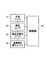
- a manufacturing system of a display panel A according to an embodiment of the present invention is a bonding unit in which the electro-optical panel 1 and the substrate 2 are superimposed in the Z direction so as to sandwich the liquid adhesive 3.
- a transport unit 20 for transporting the stacked electro-optical panel 1 and the substrate 2 into the atmosphere
- a bubble-free alignment unit 30 for aligning the electro-optical panel 1 and the substrate 2 in the XY ⁇ direction
- the aligned electro-optical panel 1 A curing unit 40 for curing the liquid adhesive 3 disposed between the substrates 2, and a control unit 50 for controlling the operation of the bonding unit 10, the transport unit 20, the bubble-free alignment unit 30, the curing unit 40 and the like. It is equipped as a main component.
- the electro-optical panel 1 includes an electro-optical material layer and means for applying a voltage to the electro-optical material layer, and changes the state of the electro-optical material layer by applying a voltage based on an electrical signal to extract desired light.
- the electro-optical panel 1 include, for example, a liquid crystal display (LCD), an organic EL display (OLED), a plasma display (PDP), and a flexible display, which are used for touch panels, 3D (three-dimensional) displays, electronic books, etc.
- LCD liquid crystal display
- OLED organic EL display
- PDP plasma display
- FPD Flat panel display
- the electro-optical panel 1 is formed in a rectangular shape or the like, and that an alignment mark (not shown) used for alignment with the substrate 2 described later is provided on the periphery thereof. Moreover, as the electro-optical panel 1, it is also possible to use one sheet before separation in which a plurality of the electro-optical panels 1 are juxtaposed in the manufacturing stage.
- the substrate 2 is made of a translucent material such as glass, quartz, or plastic, and transmits light emitted from the electro-optical panel 1 and emits the light to the Z direction side (viewing side). Have functions according to their application.
- Specific examples of the substrate 2 include cover glass and barrier glass used in touch panels, 3D (three-dimensional) displays, electronic books, etc.
- cover glass and barrier glass used in touch panels, 3D (three-dimensional) displays, electronic books, etc.
- patterns such as patterns and symbols are It is printed on the surface which is the adhesive surface.
- the size and the planar shape of the substrate 2 are formed in the same rectangular shape as that of the electro-optical panel 1, and it is preferable to provide an alignment mark (not shown) used for alignment with the electro-optical panel 1 .
- the substrate 2 it is also possible to use one substrate before separation in which a plurality of substrates 2 are juxtaposed in the manufacturing stage.
- the liquid adhesive 3 is made of a photo-curable adhesive, a thermosetting adhesive, a two-component mixture-curable adhesive, or the like, which absorbs light energy and hardens as polymerization proceeds to develop adhesiveness.
- degree of polymerization hardening degree
- the degree of polymerization hardening degree
- the liquid adhesive 3 is partially applied to the opposing surfaces (surfaces) 1a and 2a of the electro-optical panel 1 and the substrate 2, and the opposing surfaces of the electro-optical panel 1 and the substrate 2 are combined in a bonding unit 10 described later.
- the liquid adhesive 3 is extended along the facing surfaces 1a and 2a, and finally, substantially the entire facing surfaces 1a and 2a are filled.
- an ultraviolet curing adhesive or the like is used.
- the dots are drawn on the opposing surfaces 1 a and 2 a in a line or a line,
- the point-like or linear liquid adhesive 3 is extended so that the interfaces are in contact and mutually connected. It is preferable to distribute them.
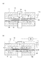
- the bonding unit 10 is entirely or partially shown in the Z direction in the vacuum chamber 11 and the vacuum chamber 11 formed in the Z direction (FIGS. 2A and 2B).
- a pair of holding plates 12 and 13 are provided facing each other in the vertical direction and detachably hold the electro-optical panel 1 and the substrate 2, and one or both of the holding plates 12 and 13
- An elevation drive unit 14 is provided to move the electro-optical panel 1 and the substrate 2 in close proximity to each other in the Z direction.
- the pair of holding plates 12 and 13 is formed of, for example, a rigid body such as metal or ceramic in a flat plate shape having a thickness that is not distorted (flexed), and the electro-optical panel 1 or the substrate 2
- As holding means (not shown) for detachably holding the adhesive for example, an adhesive chuck or a combination with an electrostatic chuck or a suction chuck, etc. are provided, and either or both of the holding surfaces 12a and 13a with respect to the vacuum chamber 11 Are reciprocally supported so as to approach or separate from each other in a parallel state in the Z direction.
- the electro-optical panel 1 is held by the holding surface 12a of the holding plate 12 disposed below, and the substrate 2 is held by the holding surface 13a of the holding plate 13 disposed above.
- the upper holding plate 13 with respect to the lower holding plate 12 is moved up and down by the raising and lowering drive unit 14.
- the lower holding plate 12 holds the substrate 2
- the upper holding plate 13 holds the electro-optical panel 1 or the lower holding plate 12 with respect to the upper holding plate 13. It is also possible to move up and down only by the lifting drive unit 14 or to move up and down by the lifting drive unit 14 both the lower holding plate 12 and the upper holding plate 13.
- a closed space S capable of adjusting the air pressure is formed around the holding plates 12 and 13 inside the vacuum chamber 11, and the closed space S is maintained under an environment of vacuum or a pressure reduced to a state close thereto. It is preferable to move the surfaces 12 a and 13 a close to each other to overlap the electro-optical panel 1 and the substrate 2.
- the transport unit 20 is, for example, a transport robot having a suction pad as a means for detachably holding the electro-optical panel 1 and the substrate 2, and at least the vacuum chamber 11 of the bonding unit 10 and the bubble-free alignment unit described later
- the electro-optical panel 1 and the substrate 2 stacked in the bonding unit 10 are conveyed to the bubble-free alignment unit 30 and delivered.
- the transfer unit 20 the electric elements stacked in the vacuum chamber 11 by operating in cooperation with liftable lift pins (not shown) provided on the holding plates 12 and 13 of the bonding unit 10, etc.
- the optical panel 1 and the substrate 2 are received from the holding surfaces 12a and 13a, taken out from the inside of the vacuum chamber 11 to the outside atmosphere, and a bubble-free alignment unit 30 described later while maintaining the overlapping state of the electro-optical panel 1 and the substrate 2. It is conveyed toward the center and set at a predetermined position on the holding chuck 31. Furthermore, if necessary, the electro-optical panel 1 and the substrate 2 are directed into the vacuum chamber 11 of the bonding unit 10 from the external area where the coating unit comprising a liquid metering dispenser such as a dispenser is disposed by the transport unit 20.
- the electro-optical panel 1 and the substrate 2 are unloaded from the bubble-free alignment unit 30 It is preferable to control the movement as follows.
- the transport unit 20 in order to promote the natural extension of the liquid adhesive 3 sandwiched in the opposing surfaces 1a and 2a with respect to the electro-optical panel 1 and the substrate 2 during transport, It is also possible to provide means for giving a proper vibration including fine vibration, or to provide buffer means for holding and holding the electro-optical panel 1 and the substrate 2 during transport for a certain period of time.
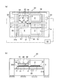
- the bubble-free alignment unit 30 is disposed in the atmosphere, and holds a pair of holding chucks 31 and 32 for detachably holding the electro-optical panel 1 and the substrate 2 conveyed by the conveyance unit 20, and the holding chucks 31 and 32.
- Horizontal drive unit 33 which aligns the electro-optical panel 1 and the substrate 2 by moving one of them in the XY.theta. Direction (up and down, left and right and diagonal direction in the example shown in FIG. 3A) with respect to the other;
- the optical panel 1 and a position detection unit 34 for detecting alignment marks and the like arranged on the peripheral edge of the substrate 2 are provided.
- the pair of holding chucks 31 and 32 are formed of, for example, a rigid body such as metal or ceramic and formed in a flat plate shape having a thickness that is not distorted (flexible), and the electro-optical panel 1 or the substrate 2
- a suction chuck, an electrostatic chuck, an adhesive chuck, a friction chuck, or a combination thereof is provided as holding means (not shown) for detachably holding the holding surface 31a and 32a.
- One of the surfaces 12a and 13a is supported movably in the XY ⁇ direction while maintaining a parallel state with respect to the other. In the example shown in FIGS.
- a camera as the position detection unit 34 is provided at the peripheral edge portion of the upper holding chuck 32 on which the substrate 2 is held. Furthermore, the lower holding chuck 31 holding the electro-optical panel 1 is supported movably in the XY ⁇ direction with respect to the upper holding chuck 32 holding the substrate 2. Further, although not shown as another example, the upper holding chuck 32 holding the substrate 2 can be supported movably in the XY ⁇ direction with respect to the lower holding chuck 31 holding the electro-optical panel 1 It is.
- the curing unit 40 irradiates light energy to increase the degree of polymerization (degree of curing) of the liquid adhesive 3, and immediately after the alignment of the electro-optical panel 1 and the substrate 2 by the non-bubble alignment unit 30, Increase the degree of polymerization (degree of curing) of the liquid adhesive 3 without moving it.
- the curing unit 40 when the liquid adhesive 3 is an ultraviolet-curable adhesive or the like, it becomes a UV irradiation unit that irradiates ultraviolet light, between the opposing surfaces 1a and 2a of the electro-optical panel 1 and the substrate 2. Ultraviolet rays are directed to a part or all of the liquid adhesive 3 extended along the same. In the example shown in FIGS.
- a UV irradiation head is disposed as a curing unit 40 at the periphery of the upper holding chuck 32 where the substrate 2 is held, and the electro-optical panel 1 and the substrate 2 are By partially curing several parts of the peripheral portion of the liquid adhesive 3 extended along the space between the facing surfaces 1a and 2a, temporary minimum curing is performed, and from the bubble-free alignment unit 30 to the electro-optical panel After the substrate 1 and the substrate 2 are carried out, the main curing is performed.
- a thermosetting adhesive, a two-component mixed curing adhesive, or the like instead of the ultraviolet curing adhesive, or to fully cure the entire liquid adhesive 3 is there.
- the control unit 50 is electrically connected to the opening / closing drive unit 11a, the lift drive unit 14, the transport unit 20, the horizontal drive unit 33, the position detection unit 34, the curing unit 40, etc. It is a controller that connects in sequence and is controlled to operate sequentially according to a preset program. In particular, the control unit 50 adjusts the operating speed of the transfer unit 20, etc., from the time when the superposition of the electro-optical panel 1 and the substrate 2 in the vacuum chamber 11 is completed by the bonding unit 10, The time until the alignment of the electro-optical panel 1 with the substrate 2 is started can be arbitrarily set.
- the time when the alignment by the bubble-free alignment unit 30 is started can be arbitrarily set. ing. That is, the liquid adhesive 3 partially applied to the opposing surfaces 1a and 2a of the electro-optical panel 1 and the substrate 2 is naturally extended along the opposing surfaces 1a and 2a of the electro-optical panel 1 and the substrate 2, While filling substantially the entire facing surfaces 1a and 2a, the local vacuum in the liquid adhesive 3 disappears and the liquid adhesive 3 becomes substantially stationary and the layer thickness of the liquid adhesive 3 is opposed After the surfaces 1a and 2a are substantially uniform in the Z direction, alignment of the electro-optical panel 1 and the substrate 2 by the bubble-free alignment unit 30 is started.
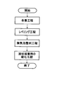
- a bonding step for overlapping the electro-optical panel 1 and the substrate 2 includes a leveling step for naturally extending 3, a bubble-free alignment step for aligning the electro-optical panel 1 and the substrate 2, and a curing step for curing the liquid adhesive 3.
- the facing surfaces 1a and 2a of the electro-optical panel 1 and the substrate 2 are in the Z direction so that the liquid adhesive 3 is sandwiched therebetween. Superimpose and temporarily bond.
- the electro-optical panel 1 and the substrate 2 which have been completely stacked are taken out from the vacuum chamber 11 by the transfer unit 20 or the like, and they are stacked in the bonding step for a predetermined time before setting in the bubbleless alignment unit 30.
- the liquid adhesive 3 is naturally stretched along the facing surfaces 1a and 2a of the electro-optical panel 1 and the substrate 2 for a predetermined time to fill substantially the entire facing surfaces 1a and 2a, and a layer of the liquid adhesive 3
- the thickness is made substantially uniform in the Z direction across the opposing surfaces 1 a and 2 a of the electro-optical panel 1 and the substrate 2.
- either the electro-optical panel 1 or the substrate 2 is slid relative to the other in the atmosphere in the XY ⁇ direction and aligned by the bubble-free alignment unit 30 with respect to the other.
- the facing surfaces of the electro-optical panel 1 and the substrate 2 in the vacuum chamber 11 by the bonding unit 10 1a and 2a are superimposed on each other in the Z direction with the liquid adhesive 3 interposed therebetween.
- the liquid adhesive 3 is forcibly extended along the facing surfaces 1a and 2a, and the liquid adhesive 3 fills the majority of the facing surfaces 1a and 2a.
- the transport unit 20 transports the electro-optical panel 1 and the substrate 2 completed in the vacuum chamber 11 from the inside of the vacuum chamber 11 to the bubble-free alignment unit 30 in the atmosphere for a predetermined time.
- the liquid adhesive 3 is naturally stretched between the electro-optical panel 1 and the substrate 2.
- the local vacuum or the like in the liquid adhesive 3 disappears, and the liquid adhesive 3 is in a substantially stationary stable state, and the layer thickness of the liquid adhesive 3 becomes the opposing surface of the electro-optical panel 1 and the substrate 2
- the whole of 1a and 2a becomes substantially uniform in proportion to the volume of the liquid adhesive 3 applied in the Z direction.
- the opposing surfaces 1a and 2a of the electro-optical panel 1 and the substrate 2 become parallel to each other, and no further gap adjustment is necessary.
- the bubble-free alignment unit 3 aligns one of the electro-optical panel 1 and the substrate 2 in the atmosphere with respect to the other in the XY ⁇ direction.
- the liquid adhesive 3 does not deform and flow, it does not involve air.
- a pattern such as a pattern or a symbol is printed on the adhesive surface like the cover glass of a touch panel, for example, and the substrate 2 has slight unevenness between the printed portion and the non-printed portion, slight unevenness is generated.
- the liquid adhesive 3 bites in a non-bubble state and the interface between the solid and the liquid conforms, the liquid adhesive 3 moves smoothly as the fluid operation of the liquid adhesive 3 itself. Therefore, the electro-optical panel 1 and the substrate 2 can be bonded in a perfect non-bubble state and at a uniform gap.
- the bonding unit 10 and the bubble-free alignment unit 30 are separately provided, and a plurality of sets of the electro-optical panel 1 and the substrate 2 are simultaneously provided in the vacuum chamber 11. These are stacked and transported by the transport unit 20, and the plurality of sets of the electro-optical panel 1 and the substrate 2 are sequentially aligned. That is, the bonding unit 10 holds the plurality of sets of the electro-optical panel 1 and the substrate 2 so as to face each other by the holding plates 12 and 13 in the vacuum chamber 11 and moves them close to each other at the same time.
- a plurality of sets of electro-optical panels 1 and substrates 2 are detachably held and sequentially aligned.
- the vacuum chamber 11 of the bonding unit 10 is configured to be entirely divisible in the Z direction, and the closed space S formed therein is a predetermined vacuum. After reaching the predetermined temperature, the plurality of electro-optical panels 1 and the substrate 2 are stacked, and thereafter the closed space S is an open-type vacuum chamber in which the open space S is open to the atmosphere.
- the vacuum chamber 11 is inseparable and an entrance is opened in a part of the side wall, and a door is supported so as to cover the entrance so as to cover the entrance.
- the electro-optical panel 1 and the substrate 2 can be moved in and out by the transport unit 20 when the door is opened.
- the plurality of electro-optical panels 1 one sheet before the separation in which the plurality of electro-optical panels 1 are juxtaposed in the manufacturing stage is held on the lower holding plate 12;
- the plurality of separated substrates 2 are held on the upper holding plate 13 so as to face the panel 1 respectively.
- a plurality of substrates 2 are held one by one before separation in which a plurality of substrates 2 are juxtaposed in the manufacturing stage. It is also possible to hold a plurality of separated electro-optical panels 1 facing each other.
- the upper holding chuck 32 for holding the substrate 2 with respect to the lower holding chuck 31 for holding the electro-optical panel 1 corresponds to each electro-optical panel 1 and
- the horizontal drive unit 33 movably supports the respective substrates 2 in the XY ⁇ directions (upper and lower, left and right directions and oblique directions in the example shown in FIG. 3A) such that the respective substrates 2 face each other.
- the plurality of sets of the electro-optical panel 1 and the respective substrates 2 can be stacked only once with respect to the bonding unit 10. Alignment and alignment are performed. Thereby, there is an advantage that the plurality of sets of electro-optical panels 1 and the substrate 2 can be efficiently bonded. As a result, the productivity of the display panel A can be improved and the cost can be reduced, as compared with the conventional manufacturing system and method in which the electro-optical panel and the substrate are superposed and aligned one by one.
- the bonding unit 10 and the bubble-free alignment unit 30 are separately disposed, and are transported by the transport unit 20 between the two, but the present invention is not limited thereto.
- the bubble alignment unit 30 may be integrally disposed, and may be transported by the transport unit 20 therein.
Priority Applications (6)
| Application Number | Priority Date | Filing Date | Title |
|---|---|---|---|
| PCT/JP2010/064734 WO2012029110A1 (ja) | 2010-08-30 | 2010-08-30 | 表示パネルの製造方法及びその製造システム |
| CN201080003057.7A CN102598091B (zh) | 2010-08-30 | 2010-08-30 | 显示面板的制造方法及其制造系统 |
| KR1020137017175A KR101614591B1 (ko) | 2010-08-30 | 2010-08-30 | 표시 패널의 제조 방법 및 그 제조 시스템 |
| JP2010541632A JP4657387B1 (ja) | 2010-08-30 | 2010-08-30 | 表示パネルの製造方法及びその製造システム |
| KR1020117006811A KR101471705B1 (ko) | 2010-08-30 | 2010-08-30 | 표시 패널의 제조 방법 및 그 제조 시스템 |
| TW099135508A TW201209780A (en) | 2010-08-30 | 2010-10-18 | Display panel production method and production system thereof |
Applications Claiming Priority (1)
| Application Number | Priority Date | Filing Date | Title |
|---|---|---|---|
| PCT/JP2010/064734 WO2012029110A1 (ja) | 2010-08-30 | 2010-08-30 | 表示パネルの製造方法及びその製造システム |
Publications (1)
| Publication Number | Publication Date |
|---|---|
| WO2012029110A1 true WO2012029110A1 (ja) | 2012-03-08 |
Family
ID=43952780
Family Applications (1)
| Application Number | Title | Priority Date | Filing Date |
|---|---|---|---|
| PCT/JP2010/064734 WO2012029110A1 (ja) | 2010-08-30 | 2010-08-30 | 表示パネルの製造方法及びその製造システム |
Country Status (5)
| Country | Link |
|---|---|
| JP (1) | JP4657387B1 (zh) |
| KR (2) | KR101614591B1 (zh) |
| CN (1) | CN102598091B (zh) |
| TW (1) | TW201209780A (zh) |
| WO (1) | WO2012029110A1 (zh) |
Cited By (4)
| Publication number | Priority date | Publication date | Assignee | Title |
|---|---|---|---|---|
| JP2013218198A (ja) * | 2012-04-11 | 2013-10-24 | Hitachi High-Technologies Corp | 基板貼り合わせ装置 |
| JP5512061B1 (ja) * | 2013-06-27 | 2014-06-04 | 信越エンジニアリング株式会社 | 貼合デバイスの製造方法 |
| JP2014214165A (ja) * | 2013-04-22 | 2014-11-17 | 富士通株式会社 | 接着剤による接着方法 |
| DE102018205983A1 (de) | 2017-04-27 | 2018-10-31 | Faurecia Interieur Industrie | Verfahren zum Herstellen eines Anzeigemoduls für einen Fahrgastraum eines Motorfahrzeugs |
Families Citing this family (14)
| Publication number | Priority date | Publication date | Assignee | Title |
|---|---|---|---|---|
| CN102598091B (zh) | 2010-08-30 | 2014-09-10 | 信越工程株式会社 | 显示面板的制造方法及其制造系统 |
| CN103009776B (zh) * | 2011-09-24 | 2017-09-22 | 宸鸿科技(厦门)有限公司 | 基板的贴合方法 |
| JP2013167712A (ja) * | 2012-02-15 | 2013-08-29 | Hitachi High-Technologies Corp | 基板の貼り合せ装置及び基板の貼り合せ方法 |
| KR101439876B1 (ko) * | 2012-12-13 | 2014-09-16 | 주식회사 성우하이텍 | 패널 접합방법 |
| JP5346116B1 (ja) * | 2012-12-19 | 2013-11-20 | 信越エンジニアリング株式会社 | ワーク貼合方法及びワーク貼合装置 |
| ITTV20120241A1 (it) * | 2012-12-21 | 2014-06-22 | Dario Toncelli | Metodo ed impianto per realizzare pannelli formati con lastre incollate |
| CN104022057A (zh) * | 2013-02-28 | 2014-09-03 | 株式会社日立高新技术 | 基板贴合装置以及基板贴合用具 |
| JP5422767B1 (ja) * | 2013-05-09 | 2014-02-19 | 信越エンジニアリング株式会社 | 貼り合わせ分離方法及び分離装置 |
| JP5395306B1 (ja) * | 2013-08-13 | 2014-01-22 | 信越エンジニアリング株式会社 | 貼合デバイスの製造装置及び貼合デバイスの製造方法 |
| JP2015158603A (ja) * | 2014-02-24 | 2015-09-03 | 株式会社Sat | 基板の貼り合せ装置 |
| TWI532588B (zh) * | 2014-02-24 | 2016-05-11 | To prevent the bubble generated by the adhesive tape and electronic components of the method | |
| CN104635369A (zh) * | 2015-03-13 | 2015-05-20 | 信利光电股份有限公司 | 液晶模组的制作方法及液晶模组 |
| TWI596070B (zh) * | 2016-05-11 | 2017-08-21 | 登峰製造股份有限公司 | 顯示面板之貼合裝置及貼合方法 |
| CN112147803A (zh) * | 2019-06-26 | 2020-12-29 | 夏普株式会社 | 贴合基板的制造方法以及基板贴合装置 |
Citations (6)
| Publication number | Priority date | Publication date | Assignee | Title |
|---|---|---|---|---|
| JPH07114010A (ja) * | 1993-10-14 | 1995-05-02 | Matsushita Electric Ind Co Ltd | 液晶表示装置 |
| JPH08190099A (ja) * | 1995-01-11 | 1996-07-23 | Fujitsu Ltd | 液晶表示装置の製造方法及び液晶表示装置の製造装置 |
| JP2002229044A (ja) * | 2000-11-30 | 2002-08-14 | Fujitsu Ltd | 貼合せ基板製造装置 |
| JP2006189861A (ja) * | 2004-12-28 | 2006-07-20 | Chi Mei Optoelectronics Corp | 液晶表示パネルの製造方法と基板組立装置 |
| JP2007079374A (ja) * | 2005-09-16 | 2007-03-29 | Seiko Epson Corp | 電気光学装置の製造方法 |
| JP2009103833A (ja) * | 2007-10-22 | 2009-05-14 | Sharp Corp | 表示装置 |
Family Cites Families (4)
| Publication number | Priority date | Publication date | Assignee | Title |
|---|---|---|---|---|
| CN100456088C (zh) * | 2002-02-05 | 2009-01-28 | 乐金显示有限公司 | Lcd粘接机和用这种粘接机制造lcd的方法 |
| JP2006071766A (ja) * | 2004-08-31 | 2006-03-16 | Makushisu Wan:Kk | 光学部品の製造装置及び製造方法 |
| KR20070051422A (ko) * | 2005-11-15 | 2007-05-18 | 삼성전자주식회사 | 액정 표시 패널의 편광판 부착 장치와 방법 및 이를 이용한액정 표시 패널의 제조 방법 |
| CN102598091B (zh) | 2010-08-30 | 2014-09-10 | 信越工程株式会社 | 显示面板的制造方法及其制造系统 |
-
2010
- 2010-08-30 CN CN201080003057.7A patent/CN102598091B/zh active Active
- 2010-08-30 JP JP2010541632A patent/JP4657387B1/ja not_active Expired - Fee Related
- 2010-08-30 KR KR1020137017175A patent/KR101614591B1/ko active IP Right Grant
- 2010-08-30 WO PCT/JP2010/064734 patent/WO2012029110A1/ja active Application Filing
- 2010-08-30 KR KR1020117006811A patent/KR101471705B1/ko active IP Right Grant
- 2010-10-18 TW TW099135508A patent/TW201209780A/zh not_active IP Right Cessation
Patent Citations (6)
| Publication number | Priority date | Publication date | Assignee | Title |
|---|---|---|---|---|
| JPH07114010A (ja) * | 1993-10-14 | 1995-05-02 | Matsushita Electric Ind Co Ltd | 液晶表示装置 |
| JPH08190099A (ja) * | 1995-01-11 | 1996-07-23 | Fujitsu Ltd | 液晶表示装置の製造方法及び液晶表示装置の製造装置 |
| JP2002229044A (ja) * | 2000-11-30 | 2002-08-14 | Fujitsu Ltd | 貼合せ基板製造装置 |
| JP2006189861A (ja) * | 2004-12-28 | 2006-07-20 | Chi Mei Optoelectronics Corp | 液晶表示パネルの製造方法と基板組立装置 |
| JP2007079374A (ja) * | 2005-09-16 | 2007-03-29 | Seiko Epson Corp | 電気光学装置の製造方法 |
| JP2009103833A (ja) * | 2007-10-22 | 2009-05-14 | Sharp Corp | 表示装置 |
Cited By (6)
| Publication number | Priority date | Publication date | Assignee | Title |
|---|---|---|---|---|
| JP2013218198A (ja) * | 2012-04-11 | 2013-10-24 | Hitachi High-Technologies Corp | 基板貼り合わせ装置 |
| CN103376586A (zh) * | 2012-04-11 | 2013-10-30 | 株式会社日立高新技术 | 基板粘合装置 |
| JP2014214165A (ja) * | 2013-04-22 | 2014-11-17 | 富士通株式会社 | 接着剤による接着方法 |
| JP5512061B1 (ja) * | 2013-06-27 | 2014-06-04 | 信越エンジニアリング株式会社 | 貼合デバイスの製造方法 |
| WO2014207867A1 (ja) * | 2013-06-27 | 2014-12-31 | 信越エンジニアリング株式会社 | 貼合デバイスの製造方法 |
| DE102018205983A1 (de) | 2017-04-27 | 2018-10-31 | Faurecia Interieur Industrie | Verfahren zum Herstellen eines Anzeigemoduls für einen Fahrgastraum eines Motorfahrzeugs |
Also Published As
| Publication number | Publication date |
|---|---|
| TW201209780A (en) | 2012-03-01 |
| KR20130086654A (ko) | 2013-08-02 |
| JP4657387B1 (ja) | 2011-03-23 |
| JPWO2012029110A1 (ja) | 2013-10-28 |
| CN102598091B (zh) | 2014-09-10 |
| KR101471705B1 (ko) | 2014-12-10 |
| CN102598091A (zh) | 2012-07-18 |
| KR101614591B1 (ko) | 2016-04-21 |
| TWI356359B (zh) | 2012-01-11 |
| KR20120033297A (ko) | 2012-04-06 |
Similar Documents
| Publication | Publication Date | Title |
|---|---|---|
| WO2012029110A1 (ja) | 表示パネルの製造方法及びその製造システム | |
| JP5456657B2 (ja) | 平面表示装置の製造方法及びこのための貼り合わせ圧締装置 | |
| KR101877600B1 (ko) | 기판 반송 장치 및 기판 조립 라인 | |
| JP5456656B2 (ja) | 平面表示装置の製造方法及びこのための接着剤樹脂の塗布装置 | |
| JP5654155B1 (ja) | ワーク貼り合わせ装置 | |
| TWI592720B (zh) | Method for manufacturing the bonding device and manufacturing device for the bonding device | |
| JP5346116B1 (ja) | ワーク貼合方法及びワーク貼合装置 | |
| KR20150020310A (ko) | 접합 디바이스의 제조 장치 및 접합 디바이스의 제조 방법 | |
| TWI699582B (zh) | 貼合器件的製造裝置及製造方法 | |
| CN108602342B (zh) | 贴合器件的真空贴合装置 | |
| WO2010095215A1 (ja) | ワーク搬送装置及び真空貼り合わせ方法 | |
| JP6049820B1 (ja) | 貼合デバイスの製造装置及び製造方法 | |
| JP4576420B2 (ja) | 接着剤塗布装置、液晶表示パネル、液晶表示パネルの製造装置及び製造方法、並びに基板貼り合わせ装置 | |
| JP2012133098A (ja) | 基板組立装置 | |
| JP2017013370A (ja) | 貼合デバイスの製造装置及び製造方法 | |
| JP2015187648A (ja) | 貼合方法および貼合装置 | |
| JP2009244690A (ja) | 基板貼合せ方法および基板貼合せ装置 | |
| JP2001174835A (ja) | 液晶表示装置用ガラス基板の組立装置及び液晶表示装置製造方法 | |
| JP2013097282A (ja) | 基板組立装置 | |
| JP2017181932A (ja) | 表示装置用部材の製造装置および表示装置用部材の製造方法 | |
| JP2002365645A (ja) | 液晶表示装置の製造方法 | |
| JP2010122394A (ja) | 基板の貼合わせ方法及び基板貼合わせ装置 |
Legal Events
| Date | Code | Title | Description |
|---|---|---|---|
| WWE | Wipo information: entry into national phase |
Ref document number: 201080003057.7 Country of ref document: CN |
|
| WWE | Wipo information: entry into national phase |
Ref document number: 2010541632 Country of ref document: JP |
|
| ENP | Entry into the national phase |
Ref document number: 20117006811 Country of ref document: KR Kind code of ref document: A |
|
| 121 | Ep: the epo has been informed by wipo that ep was designated in this application |
Ref document number: 10856663 Country of ref document: EP Kind code of ref document: A1 |
|
| NENP | Non-entry into the national phase |
Ref country code: DE |
|
| 122 | Ep: pct application non-entry in european phase |
Ref document number: 10856663 Country of ref document: EP Kind code of ref document: A1 |