WO2012002240A1 - サファイア基板とその製造方法及び窒化物半導体発光素子 - Google Patents
サファイア基板とその製造方法及び窒化物半導体発光素子 Download PDFInfo
- Publication number
- WO2012002240A1 WO2012002240A1 PCT/JP2011/064355 JP2011064355W WO2012002240A1 WO 2012002240 A1 WO2012002240 A1 WO 2012002240A1 JP 2011064355 W JP2011064355 W JP 2011064355W WO 2012002240 A1 WO2012002240 A1 WO 2012002240A1
- Authority
- WO
- WIPO (PCT)
- Prior art keywords
- sapphire substrate
- nitride semiconductor
- convex portion
- mask
- etching
- Prior art date
Links
- 239000004065 semiconductor Substances 0.000 title claims abstract description 72
- 239000000758 substrate Substances 0.000 title claims abstract description 69
- 150000004767 nitrides Chemical class 0.000 title claims abstract description 57
- 229910052594 sapphire Inorganic materials 0.000 title claims abstract description 42
- 239000010980 sapphire Substances 0.000 title claims abstract description 42
- 238000004519 manufacturing process Methods 0.000 title claims description 12
- 238000005530 etching Methods 0.000 claims description 56
- 238000000034 method Methods 0.000 claims description 16
- 239000013078 crystal Substances 0.000 abstract description 24
- 238000000605 extraction Methods 0.000 abstract description 6
- 206010053759 Growth retardation Diseases 0.000 abstract description 5
- 229910002601 GaN Inorganic materials 0.000 description 12
- NBIIXXVUZAFLBC-UHFFFAOYSA-N Phosphoric acid Chemical compound OP(O)(O)=O NBIIXXVUZAFLBC-UHFFFAOYSA-N 0.000 description 6
- QAOWNCQODCNURD-UHFFFAOYSA-N Sulfuric acid Chemical compound OS(O)(=O)=O QAOWNCQODCNURD-UHFFFAOYSA-N 0.000 description 6
- 230000007547 defect Effects 0.000 description 5
- 239000000463 material Substances 0.000 description 5
- 238000001312 dry etching Methods 0.000 description 4
- 239000007789 gas Substances 0.000 description 4
- 238000001039 wet etching Methods 0.000 description 4
- KWYUFKZDYYNOTN-UHFFFAOYSA-M Potassium hydroxide Chemical compound [OH-].[K+] KWYUFKZDYYNOTN-UHFFFAOYSA-M 0.000 description 3
- -1 SiO2 Chemical compound 0.000 description 3
- VYPSYNLAJGMNEJ-UHFFFAOYSA-N Silicium dioxide Chemical compound O=[Si]=O VYPSYNLAJGMNEJ-UHFFFAOYSA-N 0.000 description 3
- 239000002253 acid Substances 0.000 description 3
- 229910000147 aluminium phosphate Inorganic materials 0.000 description 3
- 229910052782 aluminium Inorganic materials 0.000 description 2
- 230000004888 barrier function Effects 0.000 description 2
- 238000001020 plasma etching Methods 0.000 description 2
- 230000001902 propagating effect Effects 0.000 description 2
- 229910002704 AlGaN Inorganic materials 0.000 description 1
- 229910000980 Aluminium gallium arsenide Inorganic materials 0.000 description 1
- 229910015844 BCl3 Inorganic materials 0.000 description 1
- KZBUYRJDOAKODT-UHFFFAOYSA-N Chlorine Chemical compound ClCl KZBUYRJDOAKODT-UHFFFAOYSA-N 0.000 description 1
- XPDWGBQVDMORPB-UHFFFAOYSA-N Fluoroform Chemical compound FC(F)F XPDWGBQVDMORPB-UHFFFAOYSA-N 0.000 description 1
- 229910001218 Gallium arsenide Inorganic materials 0.000 description 1
- CPELXLSAUQHCOX-UHFFFAOYSA-N Hydrogen bromide Chemical compound Br CPELXLSAUQHCOX-UHFFFAOYSA-N 0.000 description 1
- 229910018503 SF6 Inorganic materials 0.000 description 1
- 229910003910 SiCl4 Inorganic materials 0.000 description 1
- 229910004298 SiO 2 Inorganic materials 0.000 description 1
- 229910052681 coesite Inorganic materials 0.000 description 1
- 150000001875 compounds Chemical class 0.000 description 1
- 229910052906 cristobalite Inorganic materials 0.000 description 1
- 230000007423 decrease Effects 0.000 description 1
- 230000006866 deterioration Effects 0.000 description 1
- 238000009792 diffusion process Methods 0.000 description 1
- XPPKVPWEQAFLFU-UHFFFAOYSA-N diphosphoric acid Chemical compound OP(O)(=O)OP(O)(O)=O XPPKVPWEQAFLFU-UHFFFAOYSA-N 0.000 description 1
- 229910052735 hafnium Inorganic materials 0.000 description 1
- 229910000042 hydrogen bromide Inorganic materials 0.000 description 1
- 239000011261 inert gas Substances 0.000 description 1
- 238000002488 metal-organic chemical vapour deposition Methods 0.000 description 1
- 229910052758 niobium Inorganic materials 0.000 description 1
- 238000000059 patterning Methods 0.000 description 1
- 230000000737 periodic effect Effects 0.000 description 1
- 230000001737 promoting effect Effects 0.000 description 1
- 229940005657 pyrophosphoric acid Drugs 0.000 description 1
- 229910052710 silicon Inorganic materials 0.000 description 1
- 239000000377 silicon dioxide Substances 0.000 description 1
- 235000012239 silicon dioxide Nutrition 0.000 description 1
- 229910052814 silicon oxide Inorganic materials 0.000 description 1
- FDNAPBUWERUEDA-UHFFFAOYSA-N silicon tetrachloride Chemical compound Cl[Si](Cl)(Cl)Cl FDNAPBUWERUEDA-UHFFFAOYSA-N 0.000 description 1
- 229910052682 stishovite Inorganic materials 0.000 description 1
- SFZCNBIFKDRMGX-UHFFFAOYSA-N sulfur hexafluoride Chemical compound FS(F)(F)(F)(F)F SFZCNBIFKDRMGX-UHFFFAOYSA-N 0.000 description 1
- 229910052715 tantalum Inorganic materials 0.000 description 1
- 229910052719 titanium Inorganic materials 0.000 description 1
- FAQYAMRNWDIXMY-UHFFFAOYSA-N trichloroborane Chemical compound ClB(Cl)Cl FAQYAMRNWDIXMY-UHFFFAOYSA-N 0.000 description 1
- 229910052905 tridymite Inorganic materials 0.000 description 1
- 229910052720 vanadium Inorganic materials 0.000 description 1
- 229910052726 zirconium Inorganic materials 0.000 description 1
Images


Classifications
-
- H—ELECTRICITY
- H01—ELECTRIC ELEMENTS
- H01L—SEMICONDUCTOR DEVICES NOT COVERED BY CLASS H10
- H01L21/00—Processes or apparatus adapted for the manufacture or treatment of semiconductor or solid state devices or of parts thereof
- H01L21/02—Manufacture or treatment of semiconductor devices or of parts thereof
- H01L21/02104—Forming layers
- H01L21/02365—Forming inorganic semiconducting materials on a substrate
- H01L21/02367—Substrates
- H01L21/02428—Structure
- H01L21/0243—Surface structure
-
- C—CHEMISTRY; METALLURGY
- C30—CRYSTAL GROWTH
- C30B—SINGLE-CRYSTAL GROWTH; UNIDIRECTIONAL SOLIDIFICATION OF EUTECTIC MATERIAL OR UNIDIRECTIONAL DEMIXING OF EUTECTOID MATERIAL; REFINING BY ZONE-MELTING OF MATERIAL; PRODUCTION OF A HOMOGENEOUS POLYCRYSTALLINE MATERIAL WITH DEFINED STRUCTURE; SINGLE CRYSTALS OR HOMOGENEOUS POLYCRYSTALLINE MATERIAL WITH DEFINED STRUCTURE; AFTER-TREATMENT OF SINGLE CRYSTALS OR A HOMOGENEOUS POLYCRYSTALLINE MATERIAL WITH DEFINED STRUCTURE; APPARATUS THEREFOR
- C30B25/00—Single-crystal growth by chemical reaction of reactive gases, e.g. chemical vapour-deposition growth
- C30B25/02—Epitaxial-layer growth
- C30B25/18—Epitaxial-layer growth characterised by the substrate
- C30B25/183—Epitaxial-layer growth characterised by the substrate being provided with a buffer layer, e.g. a lattice matching layer
-
- C—CHEMISTRY; METALLURGY
- C30—CRYSTAL GROWTH
- C30B—SINGLE-CRYSTAL GROWTH; UNIDIRECTIONAL SOLIDIFICATION OF EUTECTIC MATERIAL OR UNIDIRECTIONAL DEMIXING OF EUTECTOID MATERIAL; REFINING BY ZONE-MELTING OF MATERIAL; PRODUCTION OF A HOMOGENEOUS POLYCRYSTALLINE MATERIAL WITH DEFINED STRUCTURE; SINGLE CRYSTALS OR HOMOGENEOUS POLYCRYSTALLINE MATERIAL WITH DEFINED STRUCTURE; AFTER-TREATMENT OF SINGLE CRYSTALS OR A HOMOGENEOUS POLYCRYSTALLINE MATERIAL WITH DEFINED STRUCTURE; APPARATUS THEREFOR
- C30B25/00—Single-crystal growth by chemical reaction of reactive gases, e.g. chemical vapour-deposition growth
- C30B25/02—Epitaxial-layer growth
- C30B25/18—Epitaxial-layer growth characterised by the substrate
- C30B25/186—Epitaxial-layer growth characterised by the substrate being specially pre-treated by, e.g. chemical or physical means
-
- C—CHEMISTRY; METALLURGY
- C30—CRYSTAL GROWTH
- C30B—SINGLE-CRYSTAL GROWTH; UNIDIRECTIONAL SOLIDIFICATION OF EUTECTIC MATERIAL OR UNIDIRECTIONAL DEMIXING OF EUTECTOID MATERIAL; REFINING BY ZONE-MELTING OF MATERIAL; PRODUCTION OF A HOMOGENEOUS POLYCRYSTALLINE MATERIAL WITH DEFINED STRUCTURE; SINGLE CRYSTALS OR HOMOGENEOUS POLYCRYSTALLINE MATERIAL WITH DEFINED STRUCTURE; AFTER-TREATMENT OF SINGLE CRYSTALS OR A HOMOGENEOUS POLYCRYSTALLINE MATERIAL WITH DEFINED STRUCTURE; APPARATUS THEREFOR
- C30B29/00—Single crystals or homogeneous polycrystalline material with defined structure characterised by the material or by their shape
- C30B29/10—Inorganic compounds or compositions
- C30B29/40—AIIIBV compounds wherein A is B, Al, Ga, In or Tl and B is N, P, As, Sb or Bi
- C30B29/403—AIII-nitrides
-
- H—ELECTRICITY
- H01—ELECTRIC ELEMENTS
- H01L—SEMICONDUCTOR DEVICES NOT COVERED BY CLASS H10
- H01L21/00—Processes or apparatus adapted for the manufacture or treatment of semiconductor or solid state devices or of parts thereof
- H01L21/02—Manufacture or treatment of semiconductor devices or of parts thereof
- H01L21/02104—Forming layers
- H01L21/02365—Forming inorganic semiconducting materials on a substrate
- H01L21/02367—Substrates
- H01L21/0237—Materials
- H01L21/0242—Crystalline insulating materials
-
- H—ELECTRICITY
- H01—ELECTRIC ELEMENTS
- H01L—SEMICONDUCTOR DEVICES NOT COVERED BY CLASS H10
- H01L21/00—Processes or apparatus adapted for the manufacture or treatment of semiconductor or solid state devices or of parts thereof
- H01L21/02—Manufacture or treatment of semiconductor devices or of parts thereof
- H01L21/02104—Forming layers
- H01L21/02365—Forming inorganic semiconducting materials on a substrate
- H01L21/02518—Deposited layers
- H01L21/02521—Materials
- H01L21/02538—Group 13/15 materials
- H01L21/0254—Nitrides
-
- H—ELECTRICITY
- H01—ELECTRIC ELEMENTS
- H01L—SEMICONDUCTOR DEVICES NOT COVERED BY CLASS H10
- H01L21/00—Processes or apparatus adapted for the manufacture or treatment of semiconductor or solid state devices or of parts thereof
- H01L21/02—Manufacture or treatment of semiconductor devices or of parts thereof
- H01L21/02104—Forming layers
- H01L21/02365—Forming inorganic semiconducting materials on a substrate
- H01L21/02656—Special treatments
- H01L21/02658—Pretreatments
-
- H—ELECTRICITY
- H01—ELECTRIC ELEMENTS
- H01L—SEMICONDUCTOR DEVICES NOT COVERED BY CLASS H10
- H01L33/00—Semiconductor devices with at least one potential-jump barrier or surface barrier specially adapted for light emission; Processes or apparatus specially adapted for the manufacture or treatment thereof or of parts thereof; Details thereof
- H01L33/02—Semiconductor devices with at least one potential-jump barrier or surface barrier specially adapted for light emission; Processes or apparatus specially adapted for the manufacture or treatment thereof or of parts thereof; Details thereof characterised by the semiconductor bodies
- H01L33/12—Semiconductor devices with at least one potential-jump barrier or surface barrier specially adapted for light emission; Processes or apparatus specially adapted for the manufacture or treatment thereof or of parts thereof; Details thereof characterised by the semiconductor bodies with a stress relaxation structure, e.g. buffer layer
-
- H—ELECTRICITY
- H01—ELECTRIC ELEMENTS
- H01L—SEMICONDUCTOR DEVICES NOT COVERED BY CLASS H10
- H01L33/00—Semiconductor devices with at least one potential-jump barrier or surface barrier specially adapted for light emission; Processes or apparatus specially adapted for the manufacture or treatment thereof or of parts thereof; Details thereof
- H01L33/02—Semiconductor devices with at least one potential-jump barrier or surface barrier specially adapted for light emission; Processes or apparatus specially adapted for the manufacture or treatment thereof or of parts thereof; Details thereof characterised by the semiconductor bodies
- H01L33/26—Materials of the light emitting region
- H01L33/30—Materials of the light emitting region containing only elements of group III and group V of the periodic system
- H01L33/32—Materials of the light emitting region containing only elements of group III and group V of the periodic system containing nitrogen
Definitions
- the present invention relates to a sapphire substrate for a nitride semiconductor light emitting device, a method for manufacturing the same, and a nitride semiconductor light emitting device.
- a light emitting diode (LED) made of a nitride semiconductor is usually configured by sequentially stacking an n-type semiconductor layer, an active layer, and a p-type semiconductor layer on a sapphire substrate.
- the emitted light is extracted from the side opposite to the sapphire substrate or the sapphire substrate side, but the light emitted from the active layer is also emitted in the direction opposite to the emission side. Therefore, it is necessary to improve the external quantum efficiency by effectively extracting light emitted in the direction opposite to the emission side from the emission side.
- Patent Document 1 discloses that a plurality of triangular pyramid-shaped convex portions are arranged on a sapphire substrate to improve external quantum efficiency.
- Japanese Patent Application Laid-Open No. H10-228561 describes that the generation of voids and deterioration of crystallinity can be suppressed by growing crystals on the surface on which the convex portions are formed by the triangular frustum-shaped convex portions.
- the present invention provides a sapphire substrate for a nitride semiconductor light emitting device capable of forming a nitride semiconductor light emitting device capable of growing a nitride semiconductor excellent in crystallinity and having excellent light extraction efficiency, and
- An object is to provide a manufacturing method. It is another object of the present invention to provide a nitride semiconductor light emitting device having a nitride semiconductor having excellent crystallinity and excellent light extraction efficiency.
- a sapphire substrate according to the present invention has a plurality of convex portions on one main surface, and a nitride semiconductor is grown on one main surface to form a nitride semiconductor light emitting device.
- the convex portion has a conical shape with a sharp tip, and the inclined surface of the convex portion is grown on the nitride semiconductor as compared to the substrate surface located between adjacent convex portions, respectively. It is characterized by having a tilt change line that consists of a crystal growth suppressing surface in which the tilt angle is suppressed and the tilt angle changes discontinuously.
- the bottom surface of the convex portion is a substantially polygonal shape having three or more sides of an arc shape that bulges outward, and the inclined surface includes both ends of the sides and the pointed tip. Can be configured such that the inclination angle changes discontinuously at the inclination change line.
- each of the inclined surfaces of the convex portions preferably has an inclination angle of an inclined surface above the inclination change line smaller than an inclination angle of an inclined surface below the inclination change line.
- the convex portions are provided separately from each other on the one main surface.
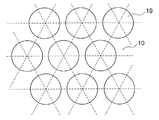
- the convex portions are periodically arranged on the one main surface, and as the periodic arrangement, at the apex of a triangular lattice, a quadrangular lattice, or a hexagonal lattice. It is mentioned to arrange periodically.
- a nitride semiconductor light emitting device includes the sapphire substrate according to the present invention, and a nitride semiconductor layer formed by growing a nitride semiconductor on one main surface of the sapphire substrate. It is characterized by that.
- a method for manufacturing a sapphire substrate for a nitride semiconductor light emitting device is a method for manufacturing a sapphire substrate for a nitride semiconductor light emitting device, in which a first mask is formed on the C surface of the sapphire substrate, and the first Etching a sapphire substrate using the mask as an etching mask to form a truncated convex truncated cone-shaped downward convex portion; Removing the first mask to expose the upper surface of the lower convex portion; and A second etching step of forming a cone-shaped upper convex portion having a sharp tip on the lower convex portion by further etching the lower convex portion exposing the upper surface; It is characterized by including.
- the sapphire substrate according to the present invention configured as described above has a plurality of convex portions formed on one main surface, each having a conical shape with pointed tips, and the inclined surfaces of the convex portions are adjacent to each other. Compared to the substrate surface located between the protrusions, it has a crystal growth suppression surface in which the growth of the nitride semiconductor is suppressed and has an inclination change line in which the inclination angle changes discontinuously. An excellent nitride semiconductor can be grown, and a nitride semiconductor light emitting device having excellent light extraction efficiency can be configured.
- FIG. 4 is a plan view illustrating an example of an array of protrusions 1 in the nitride semiconductor light emitting device of the embodiment.
- 6 is a plan view illustrating another example of the arrangement of the protrusions 1 in the nitride semiconductor light emitting device of the embodiment.
- the nitride semiconductor light emitting device In the method for manufacturing the nitride semiconductor light emitting device according to the embodiment, it is a plan view when the first mask 19 for the second etching step is formed. It is a top view of the substrate surface after the 1st etching process in the manufacturing method of the nitride semiconductor light emitting element concerning an embodiment. It is a top view of the substrate surface when the 2nd mask for the 2nd etching process in the manufacturing method of the nitride semiconductor light emitting element concerning an embodiment is formed.
- each element constituting the present invention may be configured such that a plurality of elements are constituted by the same member and the plurality of elements are shared by one member, and conversely, the function of one member is constituted by a plurality of members. It can also be realized by sharing.
- the nitride semiconductor light emitting device has a base layer 21, a first conductivity type layer (n-type layer) 22, and an active layer (light emitting layer) on a sapphire substrate 10. 23 and the second conductive type layer (p-type layer) 24 are sequentially stacked, and the surface of the substrate 10 on which the base layer 21 is grown has a cone-shaped shape with a pointed tip. A plurality of convex portions (dimples) 1 are provided.
- the nitride semiconductor light-emitting device of the embodiment configured as described above is nitrided on the surface of the substrate 10 provided with a plurality of cone-shaped convex portions (dimples) 1 with sharp tips, as will be described in detail later. Since the base layer 21 made of a semiconductor, the first conductivity type layer (n-type layer) 22, the active layer (light emitting layer) 23, and the second conductivity type layer (p-type layer) 24 are grown, the semiconductor layer is crystallized. It can grow well.
- the semiconductor light emitting device of the embodiment can efficiently reflect the light emitted from the light emitting layer 23 in the emission direction by the plurality of cone-shaped convex portions 1 having pointed tips, thereby improving the light extraction efficiency. Can be high. Specifically, the light propagating in the lateral direction can be reflected and diffracted by the convex portion 1, particularly the inclined surface of the convex portion 1.
- the convex portion (dimple) 1 is formed to have a substantially triangular pyramid shape as shown in FIGS.
- the bottom surface of the convex portion is substantially triangular (each side 11, 12, 13 is arcuately swelled outward in a substantially triangular shape),
- the three inclined surfaces 11k, 12k, and 13k of the convex portion 1 are substantially triangular shapes that swell outward, and have inclination change lines (etching switching lines) L11, L12, and L13 in the middle thereof, respectively. The slope changes discontinuously at the slope change line.
- the inclined surfaces 11k, 12k, and 13k are bent at the inclined change lines L11, L12, and L13, respectively, and above the inclined change lines L11, L12, and L13 (vertex) Side) slope is gentler than the bottom (bottom side) slope.
- the convex portion (dimple) 1 has a substantially triangular pyramid shape, and its apex t1 is sharp.
- the pointed apex means that the apex portion (upper surface) of the convex portion 1 is small enough that the nitride semiconductor does not grow from the apex of the convex portion (dimple) 1. .
- the light propagating in the surface direction of the substrate out of the light emitted from the light emitting layer 23 is the surface between the convex portions 1 on the substrate surface and the inclination of the convex portions 1. It is irregularly reflected or diffracted by the surfaces 11k, 12k, and 13k.
- the inclined surfaces 11k, 12k, and 13k of the convex portion 1 of the present embodiment are incident like a so-called convex mirror because the curved surfaces bulge outward as shown in FIGS. Since the light is diffused and reflected so as to spread, and the inclination changes discontinuously with the inclination change lines 11k, 12k, and 13k as boundaries, the incident light is diffused in a wider range.
- the substantially triangular pyramid-shaped convex portion 1 of the present embodiment is configured by setting the crystal form of the substrate, the surface orientation of the substrate surface on which the convex portion 1 is formed, the mask shape and dimensions, and the etching conditions according to the target shape. Can be formed.
- a lower convex portion 1a having a substantially triangular frustum shape is formed.
- the upper surface of the substantially triangular truncated pyramid-shaped lower convex portion 1a is etched in a substantially triangular shape and has an area smaller than that of the circular mask due to undercut.
- the bottom surface and the top surface of the lower convex portion 1a have a substantially triangular shape with an arc shape in which each side swells outward, and the area decreases as the etching progresses, and the radius of curvature of the arc on each side increases and becomes linear. become.
- the first mask is removed, and then the second mask is formed on the upper surface of the lower convex portion 1a, or etching is performed without forming the second mask.
- an upper convex portion 1b having a triangular pyramid shape is further formed on the lower convex portion 1a, and the inclined surfaces 11k, 12k, and 13k whose inclination changes discontinuously with the inclination change lines L11, L12, and L13 as boundaries are provided.
- a convex portion (dimple) 1 having a substantially triangular pyramid shape is formed.
- the sides 11, 12, and 13 of the bottom surface of the convex portion 1 are straightened by increasing the etching time.
- the inclined surfaces 11k, 12k, and 13k can be formed into a flat triangular pyramid shape, and the sides 11, 12, and 13 of the bottom surface of the convex portion 1 and the inclined surfaces 11k, 12k, and 13k are curved inward. It is also possible to form a substantially triangular pyramid shape.
- the convex portion 1 on the substrate improves the light output and light extraction efficiency, and the inclined surfaces 11k, 12k, and 13k of the convex portion 1 suppress the growth of the base layer 21 when the base layer 21 is grown.
- a base layer having a surface with few crystal defects by promoting lateral growth of the base layer grown from the surface between the convex portions 1 (hereinafter referred to as a crystal growth surface) as a surface (also referred to as a crystal growth suppression surface) 21 can be formed. Therefore, it is preferable that the convex portions constituting the crystal growth suppressing surface are uniformly distributed in the crystal growth surface, and as shown in FIGS. 3 to 4, they should be regularly separated from each other. preferable.
- FIG. 3 shows a triangular lattice point arrangement
- FIG. 4 shows a square lattice point arrangement.
- the convex portions 1 are preferably formed with high density.
- the convex portions 1 are arranged at a high density in this way, the area ratio of the crystal growth suppression surface to the crystal growth surface increases, so that the ratio of the laterally grown nitride semiconductor covering the crystal growth suppression surface increases and the growth is increased.
- the dislocations extending in the direction are confined in the underlayer 21 and the dislocations appearing on the surface can be reduced.
- the slopes above (vertex side) above the slope change lines L11, L12, L13 are gentler than the slopes below (bottom side) on the slopes 11k, 12k, 13k, respectively. Therefore, the lateral growth of the nitride semiconductor is further promoted with the inclination change lines L11, L12, and L13 as boundaries. Thereby, planarization of the surface of the grown nitride semiconductor is promoted at the same time as the nitride semiconductor having better crystallinity is formed.
- Examples of the regular and high-density arrangement of the convex portions 1 include a triangular lattice point arrangement and a square lattice point arrangement as shown in FIGS. 3 to 4, a parallelogram lattice point arrangement, a rectangular lattice point arrangement, and the like. Arrangement is mentioned.
- This regular structure may be arranged in the same rule throughout the substrate surface, or may be arranged in a different regular structure according to, for example, the electrode arrangement of the semiconductor element structure formed on the substrate. .
- the height of the convex portion 1 is in the range of 0.5 ⁇ m to 2 ⁇ m, preferably in the range of 0.7 ⁇ m to 1.2 ⁇ m.
- the interval (the interval between the narrowest portions) is preferably in the range of 0.5 ⁇ m or more and 2 ⁇ m or less, and preferably 1.5 ⁇ m or less.
- One side of the bottom surface of the convex portion 1 (a linear distance between the vertices of the bottom surface) is 0.5 ⁇ m or more and 3 ⁇ m or less, preferably 0.7 ⁇ m or more and 2 ⁇ m or less.
- the convex portion 1 can be formed by, for example, two-stage etching described below.
- etching step In this manufacturing method, first, as shown in FIG. 5, a circular first mask 19 is formed on the C-plane (0001) of the sapphire substrate 10, the substrate is etched, and then the first mask 19 is removed. As a result, the lower convex portion 1a having a substantially triangular frustum shape having a substantially triangular upper surface is formed (FIG. 6). Etching includes wet etching and dry etching, but any etching method may be used in the present invention.
- gas phase etching, plasma etching, and reactive ion etching can also be used as the dry etching, and the etching gas at that time is Cl-based, F-based gas, for example, Cl2, SiCl4, BCl3, HBr, SF6, In addition to CHF3, C4F8, CF4, etc., an inert gas such as Ar may be used.
- an etching solution for wet etching for example, in the case of the sapphire substrate of the embodiment, phosphoric acid, pyrophosphoric acid, a mixed acid obtained by adding sulfuric acid thereto, or potassium hydroxide can be used.
- the mask material is appropriately selected according to the substrate material and the etching solution in addition to the silicon oxide such as SiO2, for example, selected from the group consisting of V, Zr, Nb, Hf, Ti, Ta, and Al. And an oxide of at least one element selected from the group consisting of Si, B, and Al.
- etching step Next, as shown in FIG. 7, after removing the first mask 19, a circular second mask 20 is formed on the upper surface of the lower convex portion 1a, or the substrate 1 is further formed without forming the second mask 20. Etch. In this etching step, etching proceeds until at least an upper convex portion having a pointed tip is formed on the upper surface of the lower convex portion. This etching may be wet etching or dry etching, as in the first etching step. Moreover, the etching method can also employ
- the first etching process may be wet etching, and the second etching process may be dry etching, or vice versa. Further, the etching gas or the etchant may be changed between the first etching process and the second etching process.
- the inclined surfaces 11k and 12k made of the crystal growth suppressing surface having the sharp apex t1 on the substrate 10 and the inclination angle changing discontinuously above and below the inclination changing lines L11, L12, and L13. , 13k can be formed.
- the sapphire C surface in which a plurality of convex portions 1 having sharp edges having inclined surfaces 11k, 12k, and 13k whose inclination angles change discontinuously above and below the inclination change lines L11, L12, and L13 are formed (When a nitride semiconductor is grown on (0001), the growth of the nitride semiconductor from the inclined surfaces 11k, 12k, 13k of the convex portion 1 is suppressed (substantially does not grow).
- a nitride semiconductor grown from the surface of the sapphire C plane (0001) between the convex portions 1 grows laterally on the inclined surface of the convex portion 1 and covers the convex portion 1 as the growth proceeds, and there are few crystal defects.
- a flat GaN surface can be obtained, and a light emitting element structure in which a nitride semiconductor layer with few crystal defects is stacked on the flat GaN surface with few crystal defects can be formed.
- the light emitting element structure has a laminated structure 2 in which an active layer 23 is provided between first and second conductivity type layers 22 and 24 on a substrate.
- a first electrode and a second electrode are formed on the first conductivity type layer 22 and the second conductivity type layer 24 exposed by removing a part of the two conductivity type layer 24.
- the second electrode includes a translucent ohmic electrode formed on almost the entire surface of the second conductivity type layer 24, and a pad and a diffusion electrode formed on the translucent ohmic electrode.
- a gallium nitride compound represented by a general formula InxAlyGa1-xyN (0 ⁇ x ⁇ 1, 0 ⁇ y ⁇ 1, 0 ⁇ x + y ⁇ 1) is used as a semiconductor grown on a substrate in forming a light emitting element.
- a semiconductor material can be used.
- the binary / ternary mixed crystal can be suitably used as described later.
- the present invention can also be applied to other semiconductor materials such as GaAs, GaP compound semiconductors, AlGaAs, InAlGaP, and compound compound semiconductors.
- Example 1 A circular first mask 19 having a diameter of about 1.5 ⁇ m was periodically formed by forming and patterning an SiO 2 film on the C-plane (0001) of the sapphire substrate. Subsequently, the substrate was immersed in an etching bath using a mixed acid of phosphoric acid and sulfuric acid as an etching solution, and etched for about 5 minutes at a solution temperature of about 290 ° C. until the depth (projection height) became about 1 ⁇ m. Thereby, the downward convex part 1a was formed.
- the substrate is immersed in an etching bath using a mixed acid of phosphoric acid and sulfuric acid as an etching solution without the mask, and the tip of the convex portion is sharp at a solution temperature of about 290 ° C.
- the upper convex part 1b was formed by etching until about 1 minute.
- the substrate was transferred to an MOCVD apparatus, and a 20 nm GaN buffer layer grown at a low temperature (about 510 ° C.) on the surface of the substrate on which the convex portion 1 was formed, and GaN at a high temperature (about 1050 ° C.) thereon.
- the base layer 21 having a flat surface was formed by c-axis growth.
- an n-type layer 22 such as an n-type contact layer, an active layer 23, and a p-type layer 24 are formed on the substrate on which the base layer 21 thus obtained is formed.
- An element structure blue LED having an emission wavelength of 465 nm was produced.
- an n-side contact layer of Si (4.5 ⁇ 10 18 / cm 3) -doped GaN having a thickness of 5 ⁇ m is formed on the base layer 21 as the first conductivity type layer 22 (n-type layer), and 0 .3 ⁇ m undoped GaN layer, 0.03 ⁇ m Si (4.5 ⁇ 10 18 / cm 3) doped GaN layer, 5 nm undoped GaN layer, 4 nm undoped GaN layer, and 2 nm undoped In0.1Ga0.9N layer
- a multilayer film in which 10 layers were alternately laminated was formed.
- an undoped GaN barrier layer having a thickness of 25 nm and an In0.3Ga0.7N well layer having a thickness of 3 nm are alternately and alternately stacked, and finally the barrier layer is stacked.
- a multi-quantum well structure was formed by stacking layers.
- the second conductivity type layer (p-type layer) 24 on the active layer As the second conductivity type layer (p-type layer) 24 on the active layer, a 4 nm Mg (5 ⁇ 10 19 / cm 3) doped Al 0.15 Ga 0.85 N layer and a 2.5 nm Mg (5 ⁇ 10 19 / cm 3) doped 5 layers of In0.03Ga0.97N layers are alternately stacked, and finally, the p-side multilayer film in which the AlGaN layer is stacked, and the Mg (1 ⁇ 1020 / cm3) -doped GaN film having a thickness of 0.12 ⁇ m. A side contact layer was formed.
- ITO (about 170 nm) is formed as a translucent ohmic electrode on the surface of the p-type layer 24 which is the surface of the light emitting structure, and the ITO and the n-side contact layer are formed on the ITO.
- Rh (about 100 nm) / Pt (about 200 nm) / Au (about 500 nm) was laminated in this order.
Abstract
結晶性に優れた窒化物半導体の成長が可能で、かつ光取り出し効率に優れた窒化物半導体発光素子を構成することが可能な窒化物半導体発光素子用のサファイア基板を提供するために、そのサファイア基板は、一方の主面に複数の凸部を備え、その一方の主面に窒化物半導体が成長されて窒化物半導体発光素子が形成されるサファイア基板であって、凸部は錐形状を有し、その凸部の傾斜表面はそれぞれ、隣接する凸部間に位置する基板表面に比較して窒化物半導体の成長が抑制される結晶成長抑制表面からなり、かつ傾斜角が不連続に変化する傾斜変更線を有する。
Description
本発明は、窒化物半導体発光素子用のサファイア基板とその製造方法及び窒化物半導体発光素子に関する。
例えば、窒化物半導体からなる発光ダイオード(LED)は、通常、サファイア基板上にn型半導体層、活性層、p型半導体層を順に積層することにより構成される。この発光ダイオードでは、発光した光は、サファイア基板とは反対側、またはサファイア基板側から取り出されるが、活性層で発光した光は出射側とは逆の方向にも放射される。したがって、出射側とは逆の方向に放射された光を効果的に出射側から取り出せるようにして外部量子効率を向上させることが必要になる。
そこで、例えば、三角錐台形状の凸部をサファイア基板上に複数配置して、外部量子効率を向上させることが特許文献1に開示されている。また、特許文献1には、三角錐台形状の凸部によって、その凸部が形成された面上に結晶成長させることにより、空隙の発生や結晶性の悪化を抑制できる旨記載されている。
しかしながら、本願発明者等の鋭意研究の結果、三角錐台形状のディンプルを有する面上に成長された窒化物半導体の結晶性では必ずしも十分でないことがわかった。
すなわち、近年、発光ダイオードの高出力化が進むにつれ、従来の発光ダイオードでは顕在化しなかったような結晶欠陥による問題が顕在化するようになってきている。
すなわち、近年、発光ダイオードの高出力化が進むにつれ、従来の発光ダイオードでは顕在化しなかったような結晶欠陥による問題が顕在化するようになってきている。
そこで、本発明は、結晶性に優れた窒化物半導体の成長が可能で、かつ光取り出し効率に優れた窒化物半導体発光素子を構成することが可能な窒化物半導体発光素子用のサファイア基板とその製造方法を提供することを目的とする。
また、本発明は、結晶性に優れた窒化物半導体を有し、かつ光取り出し効率に優れた窒化物半導体発光素子を提供することを目的とする。
また、本発明は、結晶性に優れた窒化物半導体を有し、かつ光取り出し効率に優れた窒化物半導体発光素子を提供することを目的とする。
以上の目的を達成するために、本発明に係るサファイア基板は、一方の主面に複数の凸部を備え、その一方の主面に窒化物半導体が成長されて窒化物半導体発光素子が形成されるサファイア基板であって、前記凸部は先端が尖った錐形状を有し、その凸部の傾斜表面はそれぞれ、隣接する凸部間に位置する基板表面に比較して前記窒化物半導体の成長が抑制される結晶成長抑制表面からなり、かつ傾斜角が不連続に変化する傾斜変更線を有することを特徴とする。
本発明に係るサファイア基板において、前記凸部の底面は、それぞれ外側に膨らんだ円弧形状の3以上の辺を有する略多角形であり、前記傾斜表面は、前記各辺の両端と前記尖った先端を頂点とする略三角形の複数の傾斜面からなり、該傾斜面がそれぞれ前記傾斜変更線において傾斜角が不連続に変化するようにできる。
本発明に係るサファイア基板において、前記凸部の傾斜面はそれぞれ、前記傾斜変更線より上の傾斜面の傾斜角が前記傾斜変更線より下の傾斜面の傾斜角より小さくなっていることが好ましい。
本発明に係るサファイア基板においては、前記凸部が、前記一方の主面上において相互に分離して設けられていることが好ましい。
本発明に係るサファイア基板においては、前記凸部が、前記一方の主面上において周期的に配置されていることが好ましく、その周期的配置として、三角形格子、四角形格子又は六角形格子の頂点に周期的に配置することが挙げられる。
本発明に係る窒化物半導体発光素子は、前記本発明に係るサファイア基板と、該サファイア基板の一方の主面上に窒化物半導体を成長させることにより形成された窒化物半導体層と、を備えたことを特徴とする。
本発明に係る窒化物半導体発光素子用サファイア基板の製造方法は、窒化物半導体発光素子用サファイア基板の製造方法であって、サファイア基板のC面上に第1マスクを形成して、その第1マスクをエッチングマスクとしてサファイア基板をエッチングすることにより、裁頭錐台形状の下凸部を形成する第1エッチング工程と、
前記第1マスクを除去して下凸部の上面を露出させる前記第1マスク除去工程と、
前記上面を露出させた下凸部をさらにエッチングすることにより、下凸部の上に先端の尖った錐形状の上凸部を形成する第2エッチング工程と、
を含むことを特徴とする。
前記第1マスクを除去して下凸部の上面を露出させる前記第1マスク除去工程と、
前記上面を露出させた下凸部をさらにエッチングすることにより、下凸部の上に先端の尖った錐形状の上凸部を形成する第2エッチング工程と、
を含むことを特徴とする。
以上のように構成された本発明に係るサファイア基板は、一方の主面に形成された複数の凸部がそれぞれ先端が尖った錐形状を有し、その凸部の傾斜表面はそれぞれ、隣接する凸部間に位置する基板表面に比較して前記窒化物半導体の成長が抑制される結晶成長抑制表面からなりかつ傾斜角が不連続に変化する傾斜変更線を有しているので、結晶性に優れた窒化物半導体の成長が可能で、かつ光取り出し効率に優れた窒化物半導体発光素子を構成することが可能になる。
以下、発明の実施の形態について図面を参照しながら説明する。ただし、以下に説明する発光素子・装置は、本発明の技術思想を具体化するためのものであって、本発明を以下のものに特定しない。特に、以下に記載されている構成部品の寸法、材質、形状、その相対的配置等は特定的な記載がない限りは、本発明の範囲をそれのみに限定する趣旨ではなく、単なる説明例にすぎない。なお、各図面が示す部材の大きさや位置関係等は、説明を明確にするため誇張していることがある。さらに、本発明を構成する各要素は、複数の要素を同一の部材で構成して一の部材で複数の要素を兼用する態様としてもよいし、逆に一の部材の機能を複数の部材で分担して実現することもできる。
本発明に係る実施形態の窒化物半導体発光素子は、図1に示すように、サファイア基板10の上に、下地層21、第1導電型層(n型層)22、活性層(発光層)23、第2導電型層(p型層)24が順に積層された半導体積層構造2が設けられており、下地層21が成長される基板10の表面には、それぞれ先端が尖った錐形状の複数の凸部(ディンプル)1が設けられている。
以上のように構成された実施形態の窒化物半導体発光素子は、詳細後述するように、先端が尖った錐形状の複数の凸部(ディンプル)1が設けられた基板10の表面にそれぞれ窒化物半導体からなる下地層21、第1導電型層(n型層)22、活性層(発光層)23、第2導電型層(p型層)24が成長されているので、当該半導体層を結晶性良く成長させることができる。
また、実施形態の半導体発光素子は、さらに発光層23で発光した光を先端が尖った錐形状の複数の凸部1によって出射方向に効率よく反射させることが可能になり、光の取り出し効率を高くできる。
具体的には、横方向に伝播する光を凸部1、特に凸部1の傾斜した傾斜面で、反射・回折させることができる。
実施形態において、凸部(ディンプル)1は、図2(a)(b)に示すように、略三角錐形状になるように形成されており、
(i)凸部底面が略三角形状(各辺11,12,13が円弧状に外側に膨らんだ略三角形状)であり、
(ii)凸部1の3つの傾斜面11k,12k,13kはそれぞれ外側に膨らんだ略三角形状であり、かつその途中にそれぞれ傾斜変更線(エッチング切替線)L11,L12,L13を有しており、その傾斜変更線を境に傾斜が不連続に変化している。
より具体的には、各傾斜面11k,12k,13kにおいて、傾斜変更線L11,L12,L13でそれぞれ傾斜面11k,12k,13kが折れ曲がっており、傾斜変更線L11,L12,L13より上(頂点側)の傾斜が下(底面側)の傾斜より緩やかになっている。
また、凸部(ディンプル)1は略三角錐形状であって、その頂点t1は尖っている。
ここで、本明細書において、頂点が尖っているとは、凸部(ディンプル)1の頂点から窒化物半導体が成長しない程度に凸部1の頂点部分(上面)が小さくなっていることをいう。
以上のように構成された実施形態の半導体発光素子では、発光層23で発光された光のうちの基板の表面方向に伝播する光が基板表面の凸部1間の面及び凸部1の傾斜面11k,12k,13kにより乱反射又は回折される。
特に、本実施形態の凸部1の傾斜面11k,12k,13kは、図2(a)(b)に示すように、外側に膨らんだ曲面となっているので所謂凸面鏡のように入射された光が拡がるように拡散されて反射され、さらに傾斜変更線11k,12k,13kを境に傾斜が不連続に変化するので、入射された光はより広い範囲に拡散される。
特に、本実施形態の凸部1の傾斜面11k,12k,13kは、図2(a)(b)に示すように、外側に膨らんだ曲面となっているので所謂凸面鏡のように入射された光が拡がるように拡散されて反射され、さらに傾斜変更線11k,12k,13kを境に傾斜が不連続に変化するので、入射された光はより広い範囲に拡散される。
本実施形態の略三角錐形状の凸部1は、基板の結晶形態及び凸部1が形成される基板表面の面方位、マスク形状及び寸法、エッチング条件とを目的形状に応じて設定することにより形成することができる。
例えば、サファイア基板のC面からなる表面に円形の第1マスクを形成して、エッチングをすると、初期段階ではマスクが形成されていない部分がエッチングにより除去されてマスク形状がほぼそのまま反映された円形の凸部が形成されるが、エッチングが進むにつれて結晶形態に起因するエッチング速度の方向依存性(方向によるエッチングが進む速度が異なること)の影響を受けることになり、結晶形態が反映された形状になっていく。
具体的には、エッチングの進行方向によってエッチング速度が異なることから結晶形態が反映されてエッチングが進み、底部の3つの頂点と三角錐の稜線が徐々に明確になってきて、円形マスクの下に略三角錐台形状の下凸部1aが形成される。この略三角錐台形状の下凸部1aの上面は、略三角形状にエッチングされておりかつアンダーカットにより円形マスクより面積は小さくなる。また、下凸部1aの底面及び上面は、各辺が外側に膨らんだ円弧形状の略三角形状になり、エッチングが進むほど面積が小さくなるとともに各辺の円弧の曲率半径は大きくなって直線的になる。
本実施形態では、下凸部1aが形成された後、第1マスクを除去したあと、下凸部1aの上面に第2マスクを形成して、又は第2マスクを形成することなくエッチングすることによって、下凸部1aの上にさらに三角錐形状の上凸部1bが形成されて、傾斜変更線L11,L12,L13を境に傾斜が不連続に変化する傾斜面11k,12k,13kを有する略三角錐形状の凸部(ディンプル)1が形成される。
尚、本実施形態において、下凸部をエッチングにより形成する際及び上凸部をエッチングにより形成する際、エッチング時間を長くすることにより、凸部1の底面の各辺11,12,13が直線で傾斜面11k,12k,13kが平坦な三角錐形状に形成することもできるし、凸部1の底面の各辺11,12,13及び傾斜面11k,12k,13kが内側に湾曲した円弧形状の略三角錐形状に形成することも可能である。
また、基板上の凸部1は、光出力、光取り出し効率を向上させるとともに、下地層21が成長される際、凸部1の傾斜面11k,12k,13kが下地層21の成長を抑制する面(結晶成長抑制表面ともいう。)となって凸部1間の表面(以下、結晶成長表面という)から成長した下地層の横方向成長を促進して、結晶欠陥の少ない表面を有する下地層21の形成を可能にするものである。したがって、結晶成長抑制表面を構成する凸部は結晶成長表面の中に均一に分布していることが好ましく、図3~4に示すように、互いに分離されて規則的に配置されていることが好ましい。
図3は、三角格子点配置であり、図4は、正方格子点配置である。
図3は、三角格子点配置であり、図4は、正方格子点配置である。
また、結晶成長表面から縦方向に成長した窒化物半導体には、基板の格子定数と窒化物半導体の格子定数の差に起因する転位が成長方向に伸びて表面に現れる傾向があるので、基板上の凸部1は高密度に形成することが好ましい。このように凸部1を高密度に配置すると、結晶成長表面に対する結晶成長抑制表面の面積比率が高くなるので、結晶成長抑制表面を覆う横方向成長された窒化物半導体の比率が多くなり、成長方向に伸びる転位が下地層21の内部に閉じ込められて表面に現れる転位を減らすことができる。
さらに、本実施形態の凸部1は、各傾斜面11k,12k,13kにおいてそれぞれ、傾斜変更線L11,L12,L13より上(頂点側)の傾斜が下(底面側)の傾斜より緩やかになっているので、傾斜変更線L11,L12,L13を境に窒化物半導体の横方向成長がより促進される。これにより、より結晶性の良好な、窒化物半導体が形成されると同時に成長された窒化物半導体の表面の平坦化が促進される。
凸部1の規則的かつ高密度の配置としては、例えば、図3~4に示すような三角格子点配置、及び正方格子点配置の他、平行四辺形格子点配置、長方形格子点配置などの配置が挙げられる。
尚、この規則構造は、基板面内全体に同一の規則で配列してもよいし、基板上に形成する半導体素子構造の、例えば、電極配置に応じて、異なる規則構造に配置してもよい。
尚、この規則構造は、基板面内全体に同一の規則で配列してもよいし、基板上に形成する半導体素子構造の、例えば、電極配置に応じて、異なる規則構造に配置してもよい。
このように、良好な結晶性の窒化物半導体を成長させるためには、凸部1の高さは、0.5μm以上2μm以下の範囲、好ましくは0.7μm以上1.2μm以下の範囲、凸部1の間隔(最も狭い部分の間隔)は、0.5μm以上2μm以下の範囲、好ましくは1.5μm以下とすることが好ましい。
凸部1の底面の一辺(底面の頂点間の直線距離)は、0.5μm以上3μm以下、好ましくは0.7μm以上2μm以下とすることが好ましい。
凸部1の底面の一辺(底面の頂点間の直線距離)は、0.5μm以上3μm以下、好ましくは0.7μm以上2μm以下とすることが好ましい。
また、基板1上に、尖った頂点t1を有し、かつ傾斜変更線L11,L12,L13の上下で傾斜角が不連続に変化する結晶成長抑制表面からなる傾斜面11k,12k,13kを有する凸部1は、例えば、以下に説明する2段階エッチングにより形成することができる。
<第1エッチングステップ>
本製造方法では、まず、図5に示すように、サファイア基板10のC面(0001)上に円形の第1マスク19を形成して、基板をエッチングした後、第1マスク19を除去する。
これにより、略三角形状の上面を有する略三角錐台形状の下凸部1aが形成される(図6)。
エッチングには、ウェットエッチングと、ドライエッチングがあるが、本発明ではいずれのエッチング方法を用いてもよい。ドライエッチングとして具体的には気相エッチング、プラズマエッチング、反応性イオンエッチングを用いることもでき、その際のエッチングガスとしては、Cl系、F系ガス、例えばCl2、SiCl4、BCl3、HBr、SF6、CHF3、C4F8、CF4、などの他、不活性ガスのArなどが挙げられる。
ウェットエッチングのエッチング溶液としては、例えば実施例のサファイア基板の場合、リン酸、若しくはピロリン酸、又はそれに硫酸を加えた混酸、又は水酸化カリウムを用いることができる。この時、マスク材料としては、SiO2などのケイ素酸化物の他、基板材料、そのエッチング液に応じて適宜選択され、例えば、V,Zr,Nb,Hf,Ti,Ta,Alからなる群から選択される少なくとも一つの元素の酸化物、Si,B,Alからなる群から選択される少なくとも一つの元素の窒化物を挙げることができる。
<第2エッチングステップ>
次に、図7に示すように、第1マスク19を除去した後、下凸部1aの上面に円形の第2マスク20を形成して、又は第2マスク20を形成することなくさらに基板1をエッチングする。
このエッチングステップにおいては、少なくとも下凸部の上面に尖った先端を有する上凸部が形成されるまでエッチングを進める。
なお、このエッチングは、第1エッチング工程と同様、ウェットエッチングであってもよいしドライエッチングであってもよい。
また、エッチング方法は、第1エッチング工程と異なるエッチング方法を採用することもできる。すなわち、第1エッチング工程がウェットエッチングで、第2エッチング工程がドライエッチングであってもよいし、またその逆でもよい。
また、第1エッチング工程と第2エッチング工程とで、エッチングガス又はエッチング液を変更してもよい。
以上の2段階エッチングにより基板10上に、尖った頂点t1を有し、かつ傾斜変更線L11,L12,L13の上下で傾斜角が不連続に変化する結晶成長抑制表面からなる傾斜面11k,12k,13kを有する凸部1を形成することができる。
以上のようにして、傾斜変更線L11,L12,L13の上下で傾斜角が不連続に変化する傾斜面11k,12k,13kを有する先端が尖った凸部1が複数形成されたサファイアC面(0001)上に、窒化物半導体を成長させると、凸部1の傾斜面11k,12k,13kからの窒化物半導体の成長は抑制される(実質的に成長はしない)。
これにより、凸部1間のサファイアC面(0001)表面から成長した窒化物半導体が凸部1の傾斜面上を横方向に成長して、成長が進むにつれて凸部1を覆い結晶欠陥の少ない平坦なGaN表面が得られ、その結晶欠陥の少ない平坦なGaN表面上に、結晶欠陥の少ない窒化物半導体層が積層された発光素子構造を形成することが可能になる。
これにより、凸部1間のサファイアC面(0001)表面から成長した窒化物半導体が凸部1の傾斜面上を横方向に成長して、成長が進むにつれて凸部1を覆い結晶欠陥の少ない平坦なGaN表面が得られ、その結晶欠陥の少ない平坦なGaN表面上に、結晶欠陥の少ない窒化物半導体層が積層された発光素子構造を形成することが可能になる。
[発光素子]
発光素子構造は、例えば、図1に示すように、基板上に、第1,2導電型層22,24の間に活性層23が設けられた積層構造2を有し、活性層23及び第2導電型層24の一部を除去して露出させた第1導電型層22の上と第2導電型層24の上とに、第1電極と第2電極とが形成されてなる。また、第2電極は、第2導電型層24上のほぼ全面に形成された透光性オーミック電極とその透光性オーミック電極の上に形成されたパッド及び拡散電極とからなる。
発光素子構造は、例えば、図1に示すように、基板上に、第1,2導電型層22,24の間に活性層23が設けられた積層構造2を有し、活性層23及び第2導電型層24の一部を除去して露出させた第1導電型層22の上と第2導電型層24の上とに、第1電極と第2電極とが形成されてなる。また、第2電極は、第2導電型層24上のほぼ全面に形成された透光性オーミック電極とその透光性オーミック電極の上に形成されたパッド及び拡散電極とからなる。
発光素子を形成するにあたって、基板上に成長させる半導体としては、一般式InxAlyGa1-x-yN(0≦x≦1、0≦y≦1、0≦x+y≦1)で表される窒化ガリウム系化合物半導体材料を用いることができる。特に後述のようにその二元・三元混晶を好適に用いることができる。また、窒化物半導体以外に、GaAs、GaP系化合物半導体、AlGaAs、InAlGaP、系化合物半導体などの他の半導体材料にも適用することができる。
以下、本発明に係る実施例を説明する。
〔実施例1〕
サファイア基板のC面(0001)上にSiO2膜を成膜、パターンニングすることにより、直径約1.5μmの円形状の第1マスク19を周期的に形成した。
続いて、エッチング液としてリン酸と硫酸の混酸を用いたエッチング浴に基板を浸漬し、溶液の温度約290℃で深さ(凸部高さ)が約1μmとなるまで約5分エッチングした。
これにより、下凸部1aが形成された。
〔実施例1〕
サファイア基板のC面(0001)上にSiO2膜を成膜、パターンニングすることにより、直径約1.5μmの円形状の第1マスク19を周期的に形成した。
続いて、エッチング液としてリン酸と硫酸の混酸を用いたエッチング浴に基板を浸漬し、溶液の温度約290℃で深さ(凸部高さ)が約1μmとなるまで約5分エッチングした。
これにより、下凸部1aが形成された。
次に、第1マスク19を除去した後、マスク無い状態で、エッチング液としてリン酸と硫酸の混酸を用いたエッチング浴に基板を浸漬し、溶液の温度約290℃で凸部の先端が尖るまで約1分エッチングすることにより上凸部1bが形成した。
以上の工程により、高さ約1μm、テーパー角が2段階の凸部1が形成された。
以上の工程により、高さ約1μm、テーパー角が2段階の凸部1が形成された。
続いて、基板をMOCVD装置に移し、凸部1が形成された基板表面に、低温(約510℃)で成長させた20nmのGaNバッファ層と、その上に高温(約1050℃)でGaNを、c軸成長させ、表面が平坦な下地層21を形成した。
このようにして得られる下地層21が形成された基板上に、図1に示すように、n型コンタクト層などのn型層22と、活性層23と、p型層24を形成して半導体素子構造(発光波長465nmの青色LED)を作製した。
具体的には、上記下地層21の上に、第1導電型層22(n型層)として、膜厚5μmのSi(4.5×10¹⁸/cm3)ドープGaNのn側コンタクト層と、0.3μmのアンドープGaN層と、0.03μmのSi(4.5×1018/cm3)ドープGaN層と、5nmのアンドープGaN層と、4nmのアンドープGaN層と2nmのアンドープIn0.1Ga0.9N層とを繰り返し交互に10層ずつ積層された多層膜を形成した。n型層22の上の活性層23として、膜厚25nmのアンドープGaNの障壁層と、膜厚3nmのIn0.3Ga0.7Nの井戸層とを繰り返し交互に6層ずつ積層し、最後に障壁層を積層した多重量子井戸構造を形成した。活性層の上の第2導電型層(p型層)24として、4nmのMg(5×1019/cm3)ドープのAl0.15Ga0.85N層と2.5nmのMg(5×1019/cm3)ドープIn0.03Ga0.97N層とを繰り返し5層ずつ交互に積層し、最後に上記AlGaN層を積層したp側多層膜層と、膜厚0.12μmのMg(1×1020/cm3)ドープGaNのp側コンタクト層を形成した。
具体的には、上記下地層21の上に、第1導電型層22(n型層)として、膜厚5μmのSi(4.5×10¹⁸/cm3)ドープGaNのn側コンタクト層と、0.3μmのアンドープGaN層と、0.03μmのSi(4.5×1018/cm3)ドープGaN層と、5nmのアンドープGaN層と、4nmのアンドープGaN層と2nmのアンドープIn0.1Ga0.9N層とを繰り返し交互に10層ずつ積層された多層膜を形成した。n型層22の上の活性層23として、膜厚25nmのアンドープGaNの障壁層と、膜厚3nmのIn0.3Ga0.7Nの井戸層とを繰り返し交互に6層ずつ積層し、最後に障壁層を積層した多重量子井戸構造を形成した。活性層の上の第2導電型層(p型層)24として、4nmのMg(5×1019/cm3)ドープのAl0.15Ga0.85N層と2.5nmのMg(5×1019/cm3)ドープIn0.03Ga0.97N層とを繰り返し5層ずつ交互に積層し、最後に上記AlGaN層を積層したp側多層膜層と、膜厚0.12μmのMg(1×1020/cm3)ドープGaNのp側コンタクト層を形成した。
尚、半導体素子構造には、発光構造部の表面となるp型層24表面に透光性のオーミック電極として、ITO(約170nm)を形成し、そのITOの上とn側コンタクト層の上に、Rh(約100nm)/Pt(約200nm)/Au(約500nm)をこの順に積層した構造の電極を形成した。
1 凸部
1a 下凸部
1b 上凸部
2 半導体積層構造
10 基板
t1 頂点
L11,L12,L13 傾斜変更線
11k,12k,13k 傾斜面
19 第1マスク
20 第2マスク
21 下地層
22 n型層(第1導電型層)
23 活性層
24 p型層(第2導電型層)
1a 下凸部
1b 上凸部
2 半導体積層構造
10 基板
t1 頂点
L11,L12,L13 傾斜変更線
11k,12k,13k 傾斜面
19 第1マスク
20 第2マスク
21 下地層
22 n型層(第1導電型層)
23 活性層
24 p型層(第2導電型層)
Claims (9)
- 一方の主面に複数の凸部を備え、その一方の主面に窒化物半導体が成長されて窒化物半導体発光素子が形成されるサファイア基板であって、
前記凸部は先端が尖った錐形状を有し、その凸部の傾斜表面はそれぞれ、隣接する凸部間に位置する基板表面に比較して前記窒化物半導体の成長が抑制される結晶成長抑制表面からなり、かつ傾斜角が不連続に変化する傾斜変更線を有することを特徴とするサファイア基板。 - 前記凸部の底面は、それぞれ外側に膨らんだ円弧形状の3以上の辺を有する略多角形であり、前記傾斜表面は、前記各辺の両端と前記尖った先端を頂点とする略三角形の複数の傾斜面からなり、該傾斜面がそれぞれ前記傾斜変更線において傾斜角が不連続に変化する請求項1に記載のサファイア基板。
- 前記凸部の傾斜面はそれぞれ、前記傾斜変更線より上の傾斜面の傾斜角が前記傾斜変更線より下の傾斜面の傾斜角より小さくなっている請求項1又は2に記載のサファイア基板。
- 前記凸部が、前記一方の主面上において相互に分離して設けられた請求項1~3のうちのいずれか1つに記載のサファイア基板。
- 前記凸部が、前記一方の主面上において周期的に配置されている請求項1~4のうちのいずれか1つに記載のサファイア基板。
- 前記凸部が、三角形格子、四角形格子又は六角形格子の頂点に配置された請求項5記載のサファイア基板。
- 請求項1~6のうちのいずれか1つに記載のサファイア基板と、該サファイア基板の一方の主面上に窒化物半導体を成長させることにより形成された窒化物半導体層と、を備えた窒化物半導体発光素子。
- 窒化物半導体発光素子用サファイア基板の製造方法であって、
サファイア基板のC面上に第1マスクを形成して、その第1マスクをエッチングマスクとしてサファイア基板をエッチングすることにより、裁頭錐台形状の下凸部を形成する第1エッチング工程と、
前記第1マスクを除去して下凸部の上面を露出させる前記第1マスク除去工程と、
前記上面を露出させた下凸部をさらにエッチングすることにより、下凸部の上に先端の尖った錐形状の上凸部を形成する第2エッチング工程と、
を含むことを特徴とする窒化物半導体発光素子用サファイア基板の製造方法。 - 前記第1マスク除去工程と第2エッチング工程の間に、前記露出させた下凸部の上面に第2マスクを形成する第2マスク形成工程を含み、
第2エッチング工程において、前記第2マスクをエッチングマスクとして前記下凸部をさらにエッチングする請求項8記載の窒化物半導体発光素子用サファイア基板の製造方法。
Priority Applications (3)
| Application Number | Priority Date | Filing Date | Title |
|---|---|---|---|
| EP11800705.3A EP2587556B1 (en) | 2010-06-28 | 2011-06-23 | Method for manufacturing a sapphire substrate and growing a nitride semiconductor light emitting device |
| JP2012522581A JP5725023B2 (ja) | 2010-06-28 | 2011-06-23 | サファイア基板とその製造方法及び窒化物半導体発光素子 |
| EP18153527.9A EP3352229A1 (en) | 2010-06-28 | 2011-06-23 | Sapphire substrate and nitride semiconductor light emitting device |
Applications Claiming Priority (2)
| Application Number | Priority Date | Filing Date | Title |
|---|---|---|---|
| JP2010-146540 | 2010-06-28 | ||
| JP2010146540 | 2010-06-28 |
Publications (1)
| Publication Number | Publication Date |
|---|---|
| WO2012002240A1 true WO2012002240A1 (ja) | 2012-01-05 |
Family
ID=45351700
Family Applications (1)
| Application Number | Title | Priority Date | Filing Date |
|---|---|---|---|
| PCT/JP2011/064355 WO2012002240A1 (ja) | 2010-06-28 | 2011-06-23 | サファイア基板とその製造方法及び窒化物半導体発光素子 |
Country Status (5)
| Country | Link |
|---|---|
| US (1) | US8779463B2 (ja) |
| EP (2) | EP3352229A1 (ja) |
| JP (1) | JP5725023B2 (ja) |
| TW (1) | TWI608632B (ja) |
| WO (1) | WO2012002240A1 (ja) |
Cited By (13)
| Publication number | Priority date | Publication date | Assignee | Title |
|---|---|---|---|---|
| JPH0752060A (ja) * | 1993-08-13 | 1995-02-28 | Matsushita Electric Works Ltd | インパクトレンチ |
| JP2012244138A (ja) * | 2011-05-16 | 2012-12-10 | Sino-American Silicon Products Inc | Led基板及びled |
| JP2013229581A (ja) * | 2012-03-28 | 2013-11-07 | Nichia Chem Ind Ltd | サファイア基板及びその製造方法並びに窒化物半導体発光素子 |
| JP2014529195A (ja) * | 2011-09-30 | 2014-10-30 | ソウル バイオシス カンパニー リミテッドSeoul Viosys Co.,Ltd. | 凹凸パターンを有する基板、これを具備する発光ダイオード及び発光ダイオードの製造方法 |
| US20150311388A1 (en) * | 2014-04-25 | 2015-10-29 | Nichia Corporation | Nitride semiconductor element and method for manufacturing the same |
| JP2017504221A (ja) * | 2013-11-07 | 2017-02-02 | 上海芯元基半導体科技有限公司 | Iii−v族窒化物半導体エピタキシャルウエハ、当該エピタキシャルウエハを含むデバイス及びその製造方法 |
| WO2017099086A1 (ja) * | 2015-12-10 | 2017-06-15 | 王子ホールディングス株式会社 | 基板、光学素子、金型、有機発光素子、有機薄膜太陽電池、および、基板の製造方法 |
| US9773946B2 (en) | 2015-02-18 | 2017-09-26 | Nichia Corporation | Light-emitting element comprising a partitioned sapphire substrate |
| US9806232B2 (en) | 2014-05-30 | 2017-10-31 | Nichia Corporation | Nitride semiconductor element and method for manufacturing the same |
| JP2018067722A (ja) * | 2017-11-22 | 2018-04-26 | 日亜化学工業株式会社 | 窒化物半導体素子およびその製造方法 |
| JP2019220704A (ja) * | 2013-06-19 | 2019-12-26 | ルミレッズ ホールディング ベーフェー | 放射場パターンに基づくパターン形成表面特徴部を持つled |
| WO2020054792A1 (ja) * | 2018-09-14 | 2020-03-19 | 王子ホールディングス株式会社 | 突状構造体、基板、その製造方法、及び発光素子 |
| CN112236874A (zh) * | 2018-06-05 | 2021-01-15 | 株式会社小糸制作所 | 半导体生长用基板、半导体元件、半导体发光元件以及半导体元件制造方法 |
Families Citing this family (10)
| Publication number | Priority date | Publication date | Assignee | Title |
|---|---|---|---|---|
| TWI540756B (zh) * | 2010-08-06 | 2016-07-01 | Nichia Corp | 藍寶石基板及半導體發光元件 |
| JP2012124257A (ja) * | 2010-12-07 | 2012-06-28 | Toshiba Corp | 半導体発光素子及びその製造方法 |
| CN103199165A (zh) * | 2012-01-05 | 2013-07-10 | 昆山中辰矽晶有限公司 | 发光二极管基板及其加工方法与发光二级管 |
| US9269745B2 (en) | 2012-11-23 | 2016-02-23 | Seoul Viosys Co., Ltd. | Light emitting diode having a plurality of light emitting units |
| CN103325906B (zh) * | 2013-06-04 | 2016-04-27 | 江苏新广联科技股份有限公司 | 可调节led发光角度的图形衬底及其制备方法 |
| JP6183189B2 (ja) * | 2013-12-02 | 2017-08-23 | 日亜化学工業株式会社 | 発光素子の製造方法 |
| CN103871844B (zh) * | 2014-03-31 | 2017-04-05 | 海迪科(南通)光电科技有限公司 | 用于改善图形化蓝宝石衬底的底部刻蚀异常的方法 |
| JP6375890B2 (ja) * | 2014-11-18 | 2018-08-22 | 日亜化学工業株式会社 | 窒化物半導体素子及びその製造方法 |
| JP6135751B2 (ja) * | 2015-02-18 | 2017-05-31 | 日亜化学工業株式会社 | 発光素子 |
| CN114023851B (zh) * | 2021-09-09 | 2023-10-13 | 华灿光电(浙江)有限公司 | 深紫外发光二极管的外延片及其制备方法 |
Citations (2)
| Publication number | Priority date | Publication date | Assignee | Title |
|---|---|---|---|---|
| WO2005018008A1 (ja) * | 2003-08-19 | 2005-02-24 | Nichia Corporation | 半導体素子 |
| JP2008177528A (ja) | 2006-12-21 | 2008-07-31 | Nichia Chem Ind Ltd | 半導体発光素子用基板の製造方法及びそれを用いた半導体発光素子 |
Family Cites Families (1)
| Publication number | Priority date | Publication date | Assignee | Title |
|---|---|---|---|---|
| TWI413279B (zh) * | 2008-06-20 | 2013-10-21 | Toyoda Gosei Kk | Iii族氮化物半導體發光元件及其製造方法、以及燈 |
-
2011
- 2011-06-23 EP EP18153527.9A patent/EP3352229A1/en active Pending
- 2011-06-23 WO PCT/JP2011/064355 patent/WO2012002240A1/ja active Application Filing
- 2011-06-23 EP EP11800705.3A patent/EP2587556B1/en active Active
- 2011-06-23 JP JP2012522581A patent/JP5725023B2/ja active Active
- 2011-06-24 US US13/168,604 patent/US8779463B2/en active Active
- 2011-06-28 TW TW100122713A patent/TWI608632B/zh active
Patent Citations (2)
| Publication number | Priority date | Publication date | Assignee | Title |
|---|---|---|---|---|
| WO2005018008A1 (ja) * | 2003-08-19 | 2005-02-24 | Nichia Corporation | 半導体素子 |
| JP2008177528A (ja) | 2006-12-21 | 2008-07-31 | Nichia Chem Ind Ltd | 半導体発光素子用基板の製造方法及びそれを用いた半導体発光素子 |
Non-Patent Citations (3)
| Title |
|---|
| HAIYONG GAO ET AL.: "Enhancement of the light output power of InGaN/GaN light-emitting diodes grown on pyramidal patterned sapphire substrate in the micro- and nanoscale", JOURNAL OF APPLIED PHYSICS, vol. 103, 15 January 2008 (2008-01-15), pages 014314, XP012108649 * |
| JI-HAO CHENG ET AL.: "Improved crystal quality and performance of GaN-based light-emitting diodes by decreasing the slanted angle of patterned sapphire", APPLIED PHYSICS LETTERS, vol. 96, 2 February 2010 (2010-02-02), pages 051109, XP012131984 * |
| See also references of EP2587556A4 |
Cited By (28)
| Publication number | Priority date | Publication date | Assignee | Title |
|---|---|---|---|---|
| JPH0752060A (ja) * | 1993-08-13 | 1995-02-28 | Matsushita Electric Works Ltd | インパクトレンチ |
| JP2012244138A (ja) * | 2011-05-16 | 2012-12-10 | Sino-American Silicon Products Inc | Led基板及びled |
| JP2014529195A (ja) * | 2011-09-30 | 2014-10-30 | ソウル バイオシス カンパニー リミテッドSeoul Viosys Co.,Ltd. | 凹凸パターンを有する基板、これを具備する発光ダイオード及び発光ダイオードの製造方法 |
| US9337390B2 (en) | 2012-03-28 | 2016-05-10 | Nichia Corporation | Sapphire substrate and method for manufacturing the same and nitride semiconductor light emitting element |
| JP2013229581A (ja) * | 2012-03-28 | 2013-11-07 | Nichia Chem Ind Ltd | サファイア基板及びその製造方法並びに窒化物半導体発光素子 |
| US8957433B2 (en) | 2012-03-28 | 2015-02-17 | Nichia Corporation | Sapphire substrate and method for manufacturing the same and nitride semiconductor light emitting element |
| US9711685B2 (en) | 2012-03-28 | 2017-07-18 | Nichia Corporation | Sapphire substrate and method for manufacturing the same and nitride semiconductor light emitting element |
| JP2019220704A (ja) * | 2013-06-19 | 2019-12-26 | ルミレッズ ホールディング ベーフェー | 放射場パターンに基づくパターン形成表面特徴部を持つled |
| JP2017504221A (ja) * | 2013-11-07 | 2017-02-02 | 上海芯元基半導体科技有限公司 | Iii−v族窒化物半導体エピタキシャルウエハ、当該エピタキシャルウエハを含むデバイス及びその製造方法 |
| US9859465B2 (en) | 2014-04-25 | 2018-01-02 | Nichia Corporation | Nitride semiconductor element and method for manufacturing the same |
| US20150311388A1 (en) * | 2014-04-25 | 2015-10-29 | Nichia Corporation | Nitride semiconductor element and method for manufacturing the same |
| JP2015211136A (ja) * | 2014-04-25 | 2015-11-24 | 日亜化学工業株式会社 | 窒化物半導体素子およびその製造方法 |
| US9525105B2 (en) | 2014-04-25 | 2016-12-20 | Nichia Corporation | Nitride semiconductor element and method for manufacturing the same |
| US10263152B2 (en) | 2014-05-30 | 2019-04-16 | Nichia Corporation | Nitride semiconductor element and method for manufacturing the same |
| US9806232B2 (en) | 2014-05-30 | 2017-10-31 | Nichia Corporation | Nitride semiconductor element and method for manufacturing the same |
| US10461222B2 (en) | 2015-02-18 | 2019-10-29 | Nichia Corporation | Light-emitting element comprising sapphire substrate with convex portions |
| US9773946B2 (en) | 2015-02-18 | 2017-09-26 | Nichia Corporation | Light-emitting element comprising a partitioned sapphire substrate |
| JPWO2017099086A1 (ja) * | 2015-12-10 | 2018-10-04 | 王子ホールディングス株式会社 | 基板、光学素子、金型、有機発光素子、有機薄膜太陽電池、および、基板の製造方法 |
| CN108476562A (zh) * | 2015-12-10 | 2018-08-31 | 王子控股株式会社 | 基板、光学元件、模具、有机发光元件、有机薄膜太阳能电池、以及基板的制造方法 |
| US10446773B2 (en) | 2015-12-10 | 2019-10-15 | Oji Holdings Corporation | Substrate, optical element, mold, organic light-emitting element, organic thin-film solar cell, and method for producing substrate |
| WO2017099086A1 (ja) * | 2015-12-10 | 2017-06-15 | 王子ホールディングス株式会社 | 基板、光学素子、金型、有機発光素子、有機薄膜太陽電池、および、基板の製造方法 |
| CN108476562B (zh) * | 2015-12-10 | 2020-01-21 | 王子控股株式会社 | 基板、光学元件、模具、有机发光元件、有机薄膜太阳能电池、以及基板的制造方法 |
| JP2018067722A (ja) * | 2017-11-22 | 2018-04-26 | 日亜化学工業株式会社 | 窒化物半導体素子およびその製造方法 |
| CN112236874A (zh) * | 2018-06-05 | 2021-01-15 | 株式会社小糸制作所 | 半导体生长用基板、半导体元件、半导体发光元件以及半导体元件制造方法 |
| US20210257515A1 (en) * | 2018-06-05 | 2021-08-19 | Koito Manufacturing Co., Ltd. | Semiconductor growth substrate, semiconductor element, semiconductor light emitting element, and method for manufacturing semiconductor element |
| WO2020054792A1 (ja) * | 2018-09-14 | 2020-03-19 | 王子ホールディングス株式会社 | 突状構造体、基板、その製造方法、及び発光素子 |
| JPWO2020054792A1 (ja) * | 2018-09-14 | 2021-08-30 | 王子ホールディングス株式会社 | 突状構造体、基板、その製造方法、及び発光素子 |
| JP7238897B2 (ja) | 2018-09-14 | 2023-03-14 | 王子ホールディングス株式会社 | 突状構造体、発光素子用基板、その製造方法、及び発光素子 |
Also Published As
| Publication number | Publication date |
|---|---|
| EP2587556A1 (en) | 2013-05-01 |
| JP5725023B2 (ja) | 2015-05-27 |
| US8779463B2 (en) | 2014-07-15 |
| JPWO2012002240A1 (ja) | 2013-08-22 |
| EP2587556B1 (en) | 2018-05-02 |
| EP3352229A1 (en) | 2018-07-25 |
| US20110316041A1 (en) | 2011-12-29 |
| EP2587556A4 (en) | 2014-06-11 |
| TW201214766A (en) | 2012-04-01 |
| TWI608632B (zh) | 2017-12-11 |
Similar Documents
| Publication | Publication Date | Title |
|---|---|---|
| JP5725023B2 (ja) | サファイア基板とその製造方法及び窒化物半導体発光素子 | |
| JP6024533B2 (ja) | サファイア基板及びその製造方法並びに窒化物半導体発光素子 | |
| US7579205B2 (en) | Method of fabricating light emitting device and thus-fabricated light emitting device | |
| JP5707978B2 (ja) | 半導体発光素子用基板およびその製造方法、並びにその基板を用いた半導体発光素子 | |
| JP5082752B2 (ja) | 半導体発光素子用基板の製造方法及びそれを用いた半導体発光素子 | |
| JP5673581B2 (ja) | Iii族窒化物半導体発光素子の製造方法、iii族窒化物半導体発光素子、ランプ、並びに、レチクル | |
| JP6248786B2 (ja) | 窒化物半導体素子およびその製造方法 | |
| KR20060079196A (ko) | 반도체 소자 | |
| TW201306301A (zh) | 製造半導體發光二極體的方法 | |
| KR20110107618A (ko) | 질화물 반도체 발광소자 및 그 제조방법 | |
| JP2016006868A (ja) | 窒化物半導体素子およびその製造方法 | |
| JP6683237B2 (ja) | 窒化物半導体素子 | |
| US8441023B2 (en) | Semiconductor light emitting device | |
| JP2008028375A (ja) | 窒化物半導体レーザ素子 | |
| JP6443524B2 (ja) | 窒化物半導体素子およびその製造方法 | |
| JP4517770B2 (ja) | 窒化物半導体素子 | |
| JP2008263228A (ja) | 半導体発光素子およびその製造方法 | |
| JP2004304203A (ja) | 窒化物半導体基板 | |
| CN115621389A (zh) | 红光led外延结构及制备方法、红光发光二极管及制备方法 | |
| KR20100021243A (ko) | 발광 소자 및 이의 제조 방법 | |
| CN116583954A (zh) | 基板结构及其制备方法、发光器件及其制备方法 | |
| KR20120010351A (ko) | 반도체 발광소자의 제조방법 | |
| KR20120068306A (ko) | 반도체 발광소자 및 그 제조방법 |
Legal Events
| Date | Code | Title | Description |
|---|---|---|---|
| 121 | Ep: the epo has been informed by wipo that ep was designated in this application |
Ref document number: 11800705 Country of ref document: EP Kind code of ref document: A1 |
|
| WWE | Wipo information: entry into national phase |
Ref document number: 2012522581 Country of ref document: JP |
|
| WWE | Wipo information: entry into national phase |
Ref document number: 2011800705 Country of ref document: EP |
|
| NENP | Non-entry into the national phase |
Ref country code: DE |