WO2011125337A1 - 位相シフトマスクブランク及びその製造方法、並びに位相シフトマスク - Google Patents
位相シフトマスクブランク及びその製造方法、並びに位相シフトマスク Download PDFInfo
- Publication number
- WO2011125337A1 WO2011125337A1 PCT/JP2011/002090 JP2011002090W WO2011125337A1 WO 2011125337 A1 WO2011125337 A1 WO 2011125337A1 JP 2011002090 W JP2011002090 W JP 2011002090W WO 2011125337 A1 WO2011125337 A1 WO 2011125337A1
- Authority
- WO
- WIPO (PCT)
- Prior art keywords
- phase shift
- shift mask
- film
- light
- transition metal
- Prior art date
- Legal status (The legal status is an assumption and is not a legal conclusion. Google has not performed a legal analysis and makes no representation as to the accuracy of the status listed.)
- Ceased
Links
Images


Classifications
-
- G—PHYSICS
- G03—PHOTOGRAPHY; CINEMATOGRAPHY; ANALOGOUS TECHNIQUES USING WAVES OTHER THAN OPTICAL WAVES; ELECTROGRAPHY; HOLOGRAPHY
- G03F—PHOTOMECHANICAL PRODUCTION OF TEXTURED OR PATTERNED SURFACES, e.g. FOR PRINTING, FOR PROCESSING OF SEMICONDUCTOR DEVICES; MATERIALS THEREFOR; ORIGINALS THEREFOR; APPARATUS SPECIALLY ADAPTED THEREFOR
- G03F1/00—Originals for photomechanical production of textured or patterned surfaces, e.g., masks, photo-masks, reticles; Mask blanks or pellicles therefor; Containers specially adapted therefor; Preparation thereof
- G03F1/26—Phase shift masks [PSM]; PSM blanks; Preparation thereof
- G03F1/32—Attenuating PSM [att-PSM], e.g. halftone PSM or PSM having semi-transparent phase shift portion; Preparation thereof
-
- C—CHEMISTRY; METALLURGY
- C23—COATING METALLIC MATERIAL; COATING MATERIAL WITH METALLIC MATERIAL; CHEMICAL SURFACE TREATMENT; DIFFUSION TREATMENT OF METALLIC MATERIAL; COATING BY VACUUM EVAPORATION, BY SPUTTERING, BY ION IMPLANTATION OR BY CHEMICAL VAPOUR DEPOSITION, IN GENERAL; INHIBITING CORROSION OF METALLIC MATERIAL OR INCRUSTATION IN GENERAL
- C23C—COATING METALLIC MATERIAL; COATING MATERIAL WITH METALLIC MATERIAL; SURFACE TREATMENT OF METALLIC MATERIAL BY DIFFUSION INTO THE SURFACE, BY CHEMICAL CONVERSION OR SUBSTITUTION; COATING BY VACUUM EVAPORATION, BY SPUTTERING, BY ION IMPLANTATION OR BY CHEMICAL VAPOUR DEPOSITION, IN GENERAL
- C23C14/00—Coating by vacuum evaporation, by sputtering or by ion implantation of the coating forming material
- C23C14/0021—Reactive sputtering or evaporation
- C23C14/0036—Reactive sputtering
-
- C—CHEMISTRY; METALLURGY
- C23—COATING METALLIC MATERIAL; COATING MATERIAL WITH METALLIC MATERIAL; CHEMICAL SURFACE TREATMENT; DIFFUSION TREATMENT OF METALLIC MATERIAL; COATING BY VACUUM EVAPORATION, BY SPUTTERING, BY ION IMPLANTATION OR BY CHEMICAL VAPOUR DEPOSITION, IN GENERAL; INHIBITING CORROSION OF METALLIC MATERIAL OR INCRUSTATION IN GENERAL
- C23C—COATING METALLIC MATERIAL; COATING MATERIAL WITH METALLIC MATERIAL; SURFACE TREATMENT OF METALLIC MATERIAL BY DIFFUSION INTO THE SURFACE, BY CHEMICAL CONVERSION OR SUBSTITUTION; COATING BY VACUUM EVAPORATION, BY SPUTTERING, BY ION IMPLANTATION OR BY CHEMICAL VAPOUR DEPOSITION, IN GENERAL
- C23C14/00—Coating by vacuum evaporation, by sputtering or by ion implantation of the coating forming material
- C23C14/06—Coating by vacuum evaporation, by sputtering or by ion implantation of the coating forming material characterised by the coating material
-
- C—CHEMISTRY; METALLURGY
- C23—COATING METALLIC MATERIAL; COATING MATERIAL WITH METALLIC MATERIAL; CHEMICAL SURFACE TREATMENT; DIFFUSION TREATMENT OF METALLIC MATERIAL; COATING BY VACUUM EVAPORATION, BY SPUTTERING, BY ION IMPLANTATION OR BY CHEMICAL VAPOUR DEPOSITION, IN GENERAL; INHIBITING CORROSION OF METALLIC MATERIAL OR INCRUSTATION IN GENERAL
- C23C—COATING METALLIC MATERIAL; COATING MATERIAL WITH METALLIC MATERIAL; SURFACE TREATMENT OF METALLIC MATERIAL BY DIFFUSION INTO THE SURFACE, BY CHEMICAL CONVERSION OR SUBSTITUTION; COATING BY VACUUM EVAPORATION, BY SPUTTERING, BY ION IMPLANTATION OR BY CHEMICAL VAPOUR DEPOSITION, IN GENERAL
- C23C14/00—Coating by vacuum evaporation, by sputtering or by ion implantation of the coating forming material
- C23C14/06—Coating by vacuum evaporation, by sputtering or by ion implantation of the coating forming material characterised by the coating material
- C23C14/0641—Nitrides
-
- G—PHYSICS
- G03—PHOTOGRAPHY; CINEMATOGRAPHY; ANALOGOUS TECHNIQUES USING WAVES OTHER THAN OPTICAL WAVES; ELECTROGRAPHY; HOLOGRAPHY
- G03F—PHOTOMECHANICAL PRODUCTION OF TEXTURED OR PATTERNED SURFACES, e.g. FOR PRINTING, FOR PROCESSING OF SEMICONDUCTOR DEVICES; MATERIALS THEREFOR; ORIGINALS THEREFOR; APPARATUS SPECIALLY ADAPTED THEREFOR
- G03F1/00—Originals for photomechanical production of textured or patterned surfaces, e.g., masks, photo-masks, reticles; Mask blanks or pellicles therefor; Containers specially adapted therefor; Preparation thereof
- G03F1/26—Phase shift masks [PSM]; PSM blanks; Preparation thereof
-
- G—PHYSICS
- G03—PHOTOGRAPHY; CINEMATOGRAPHY; ANALOGOUS TECHNIQUES USING WAVES OTHER THAN OPTICAL WAVES; ELECTROGRAPHY; HOLOGRAPHY
- G03F—PHOTOMECHANICAL PRODUCTION OF TEXTURED OR PATTERNED SURFACES, e.g. FOR PRINTING, FOR PROCESSING OF SEMICONDUCTOR DEVICES; MATERIALS THEREFOR; ORIGINALS THEREFOR; APPARATUS SPECIALLY ADAPTED THEREFOR
- G03F1/00—Originals for photomechanical production of textured or patterned surfaces, e.g., masks, photo-masks, reticles; Mask blanks or pellicles therefor; Containers specially adapted therefor; Preparation thereof
- G03F1/54—Absorbers, e.g. of opaque materials
-
- G—PHYSICS
- G03—PHOTOGRAPHY; CINEMATOGRAPHY; ANALOGOUS TECHNIQUES USING WAVES OTHER THAN OPTICAL WAVES; ELECTROGRAPHY; HOLOGRAPHY
- G03F—PHOTOMECHANICAL PRODUCTION OF TEXTURED OR PATTERNED SURFACES, e.g. FOR PRINTING, FOR PROCESSING OF SEMICONDUCTOR DEVICES; MATERIALS THEREFOR; ORIGINALS THEREFOR; APPARATUS SPECIALLY ADAPTED THEREFOR
- G03F1/00—Originals for photomechanical production of textured or patterned surfaces, e.g., masks, photo-masks, reticles; Mask blanks or pellicles therefor; Containers specially adapted therefor; Preparation thereof
- G03F1/68—Preparation processes not covered by groups G03F1/20 - G03F1/50
-
- G—PHYSICS
- G03—PHOTOGRAPHY; CINEMATOGRAPHY; ANALOGOUS TECHNIQUES USING WAVES OTHER THAN OPTICAL WAVES; ELECTROGRAPHY; HOLOGRAPHY
- G03F—PHOTOMECHANICAL PRODUCTION OF TEXTURED OR PATTERNED SURFACES, e.g. FOR PRINTING, FOR PROCESSING OF SEMICONDUCTOR DEVICES; MATERIALS THEREFOR; ORIGINALS THEREFOR; APPARATUS SPECIALLY ADAPTED THEREFOR
- G03F7/00—Photomechanical, e.g. photolithographic, production of textured or patterned surfaces, e.g. printing surfaces; Materials therefor, e.g. comprising photoresists; Apparatus specially adapted therefor
- G03F7/20—Exposure; Apparatus therefor
- G03F7/2041—Exposure; Apparatus therefor in the presence of a fluid, e.g. immersion; using fluid cooling means
-
- H—ELECTRICITY
- H10—SEMICONDUCTOR DEVICES; ELECTRIC SOLID-STATE DEVICES NOT OTHERWISE PROVIDED FOR
- H10P—GENERIC PROCESSES OR APPARATUS FOR THE MANUFACTURE OR TREATMENT OF DEVICES COVERED BY CLASS H10
- H10P76/00—Manufacture or treatment of masks on semiconductor bodies, e.g. by lithography or photolithography
-
- B—PERFORMING OPERATIONS; TRANSPORTING
- B82—NANOTECHNOLOGY
- B82Y—SPECIFIC USES OR APPLICATIONS OF NANOSTRUCTURES; MEASUREMENT OR ANALYSIS OF NANOSTRUCTURES; MANUFACTURE OR TREATMENT OF NANOSTRUCTURES
- B82Y30/00—Nanotechnology for materials or surface science, e.g. nanocomposites
-
- Y—GENERAL TAGGING OF NEW TECHNOLOGICAL DEVELOPMENTS; GENERAL TAGGING OF CROSS-SECTIONAL TECHNOLOGIES SPANNING OVER SEVERAL SECTIONS OF THE IPC; TECHNICAL SUBJECTS COVERED BY FORMER USPC CROSS-REFERENCE ART COLLECTIONS [XRACs] AND DIGESTS
- Y10—TECHNICAL SUBJECTS COVERED BY FORMER USPC
- Y10S—TECHNICAL SUBJECTS COVERED BY FORMER USPC CROSS-REFERENCE ART COLLECTIONS [XRACs] AND DIGESTS
- Y10S977/00—Nanotechnology
- Y10S977/70—Nanostructure
- Y10S977/755—Nanosheet or quantum barrier/well, i.e. layer structure having one dimension or thickness of 100 nm or less
Definitions
- the present invention relates to a mask blank with improved light resistance, a method for manufacturing the same, and a phase shift mask.
- the present invention relates to a phase shift mask blank used for producing a phase shift mask suitable for use in an exposure apparatus that uses exposure light having a short wavelength of 200 nm or less as an exposure light source, a manufacturing method thereof, and a phase shift mask.
- a fine pattern is formed using a photolithography method. Further, a number of substrates called transfer masks are usually used for forming this fine pattern.
- This transfer mask is generally provided with a fine pattern made of a metal thin film or the like on a translucent glass substrate, and a photolithography method is also used in the production of this transfer mask.
- a mask blank having a thin film (for example, a light shielding film) for forming a transfer pattern (mask pattern) on a light-transmitting substrate such as a glass substrate is used.
- a transfer mask using this mask blank an exposure process for drawing a desired pattern on the resist film formed on the mask blank, and developing the resist film in accordance with the desired pattern drawing, the resist pattern is developed.
- the development process is formed, the etching process is to etch the thin film in accordance with the resist pattern, and the process is to remove the remaining resist pattern.
- a desired pattern is drawn on the resist film formed on the mask blank, and then a developing solution is supplied to dissolve a portion of the resist film that is soluble in the developing solution, thereby forming a resist pattern.
- a developing solution is supplied to dissolve a portion of the resist film that is soluble in the developing solution, thereby forming a resist pattern.
- the exposed portion of the thin film on which the resist pattern is not formed is dissolved by dry etching or wet etching, whereby the desired mask pattern is formed on the translucent substrate. Form.
- a transfer mask is completed.
- a halftone phase shift mask is known in addition to a binary mask having a light-shielding film pattern made of a chromium-based material on a conventional translucent substrate.
- This halftone type phase shift mask has a structure having a phase shift film made of a light semi-transmissive film on a translucent substrate, and the phase shift film made of the light semi-transmissive film does not substantially contribute to exposure. Intense light (for example, 1% to 20% with respect to the exposure wavelength) is transmitted and has a predetermined phase difference.
- This halftone type phase shift mask includes a phase shift unit patterned with a phase shift film, and a light transmission unit that does not have a phase shift film and transmits light having an intensity that substantially contributes to exposure.
- the phase of the light transmitted through the light transmission part is substantially inverted with respect to the phase of the light transmitted through the light transmission part, so that the light passes through the vicinity of the boundary between the phase shift part and the light transmission part and is diffractive.
- the lights that have entered each other's area cancel each other out, and the light intensity at the boundary is made almost zero, thereby improving the contrast, that is, the resolution of the boundary.
- a molybdenum silicide compound which is a material containing molybdenum and silicon is widely used.
- the background of the problem of mask deterioration due to repeated use of such a transfer mask is presumed as follows.
- Conventionally for example, when haze is generated, cleaning is performed to remove the haze, but film reduction (elution) due to cleaning is unavoidable, and the number of times of cleaning determines the mask life.
- the repeated use period of the mask has been extended, and the exposure time has also been extended accordingly, so that the problem of light resistance to short-wavelength light, such as ArF excimer lasers, has newly emerged. It was.
- a phase shift film containing metal and silicon as main components is 250 to 350 ° C. in the air or in an oxygen atmosphere.
- Heat treatment for 90 to 150 minutes for example, the above-mentioned Patent Document 1
- forming a cap layer mainly composed of metal and silicon on a phase shift film composed mainly of the metal and silicon for example, the above-mentioned Patent Document 2
- further improvement in the light resistance of the film against the exposure light is required as the wavelength of the exposure light source has been shortened in recent years.
- the present invention has been made to solve the conventional problems, and the object of the present invention is to provide a semi-translucent light made of a material mainly composed of transition metals, silicon and nitrogen with respect to exposure light having a wavelength of 200 nm or less. It is an object to provide a phase shift mask blank, a method for manufacturing the same, and a phase shift mask that can improve the light resistance of the film and improve the mask life.
- the inventor presumed the following factors that caused the deterioration of the transfer mask due to repeated use as the exposure light source wavelength became shorter.
- the present invention has been clarified from the results of experiments by the inventors of the present application that the effects of the present invention can be obtained by having the predetermined configuration of the present invention. It is not bound by the speculation described below.
- phase shift mask when the exposure light is accumulated, the oxidation and expansion of Si further progress, and the oxidized Mo diffuses in the altered layer and precipitates on the surface, for example, It is considered that MoO 3 is sublimated, and as a result, the thickness of the deteriorated layer gradually increases (the proportion of the deteriorated layer in the MoSi film increases).
- the phenomenon in which such an altered layer is generated and further expanded is that the energy required for the transition of the constituent atoms that trigger the oxidation reaction of Si and Mo constituting the phase shift film to occur. This is remarkably confirmed in the case of exposure light having a short wavelength such as an ArF excimer laser.
- Such a phenomenon is not limited to MoSi-based materials, and the same can be said for phase shift films made of materials containing other transition metals and silicon.
- the inventor continued further research based on the above elucidated facts and considerations.
- the transition metal (M) between the transition metal (M) and silicon is an incomplete nitride film having a transition metal (M) of less than 9%
- a complete nitride film having a transition metal (M) of less than 9% is obtained.
- the inventors have found that the change in film thickness based on the formation of the deteriorated layer can be suppressed to zero and the light resistance can be remarkably improved, and the present invention has been completed.
- the present invention has the following configuration.
- (Configuration 1) A phase shift mask blank used for producing a phase shift mask to which ArF excimer laser exposure light is applied, On the translucent substrate, provided with a light semi-transmissive film, The light semi-transmissive film is composed of an incomplete nitride film mainly composed of a transition metal, silicon and nitrogen, A phase shift mask blank, wherein the content ratio of the transition metal between the transition metal and silicon in the light-semitransmissive film is less than 9%.
- (Configuration 2) The phase shift mask blank according to Configuration 1, wherein the content ratio of the transition metal between the transition metal and silicon in the light-semitransmissive film is 2% or more.
- (Configuration 3) 3.
- phase shift mask blank according to Configuration 1 or 2 wherein the incomplete nitride film includes Mo—N bonds and Mo—Si bonds, and the Mo—Si bonds are relatively more contained than the Mo—N bonds. .
- (Configuration 4) 4.
- (Configuration 5) 4.
- the phase shift mask blank according to any one of configurations 1 to 3, wherein a transmittance of the light semi-transmissive film with respect to a wavelength of the exposure light is 4% or more and less than 9%.
- (Configuration 9) A phase shift mask used for producing a phase shift mask to which ArF excimer laser exposure light is applied, On the translucent substrate, provided with a light semi-transmissive film pattern, The light translucent film pattern is composed of an incomplete nitride film mainly composed of transition metal, silicon and nitrogen, The phase shift mask, wherein the transition metal content ratio between the transition metal and silicon in the light semi-transmissive film pattern is less than 9%. (Configuration 10) The phase shift mask according to Configuration 9, wherein the transition metal content ratio between the transition metal and silicon in the light-semitransmissive film pattern is 2% or more. (Configuration 11) 11.
- phase shift mask according to Configuration 9 or 10 wherein the incomplete nitride film includes Mo—N bonds and Mo—Si bonds, and the Mo—Si bonds are relatively more contained than the Mo—N bonds.
- Configuration 12 The phase shift mask according to any one of Structures 9 to 11, wherein the incomplete nitride film mainly includes Si—N bonds and Mo—Si bonds.
- Configuration 13 13. The phase shift mask according to claim 9, wherein the content of nitrogen in the light semitransmissive film pattern is 40 atomic% or more and 47 atomic% or less.
- Configuration 14 The phase shift mask according to any one of Structures 9 to 13, wherein the transition metal is molybdenum.
- (Configuration 15) The phase shift mask according to any one of Structures 9 to 14, wherein a film thickness of the light semitransmissive film pattern is 75 nm or less.
- (Configuration 16) A method for producing a phase shift mask blank used for producing a phase shift mask to which ArF excimer laser exposure light is applied, By performing sputtering in an atmosphere containing nitrogen gas, forming a light semi-transmissive film mainly composed of transition metal, silicon and nitrogen on the light-transmitting substrate; The method of manufacturing a phase shift mask blank, wherein a flow rate of nitrogen gas in the atmosphere is lower than a flow rate for completely nitriding the transition metal and silicon.
- (Configuration 17) The flow rate of the nitrogen gas in the atmosphere is more than 70% and less than 95% with respect to the flow rate for completely nitriding the transition metal and silicon.
- Production method. (Configuration 18) A circuit pattern is formed on a semiconductor wafer using a transfer mask manufactured using the phase shift mask blank described in Structure 1.
- a method for manufacturing a semiconductor device comprising: (Configuration 19) A method of manufacturing a semiconductor device, wherein a circuit pattern is formed on a semiconductor wafer using the phase shift mask according to Configuration 9.
- the present invention is a phase shift mask blank used to produce a phase shift mask to which ArF excimer laser exposure light is applied, as in Configuration 1.
- the light semi-transmissive film is composed of an incomplete nitride film mainly composed of a transition metal, silicon and nitrogen,
- the phase shift mask blank is characterized in that the content ratio of the transition metal between the transition metal and silicon in the light-semitransmissive film is less than 9%.
- the incomplete nitride is a compound having a low nitrogen content with respect to the stoichiometric composition corresponding to the valence that the transition metal element or silicon element can take. That is, there are few MN bonds and Si—N bonds.
- incomplete nitride is a compound that has fewer MN bonds and Si—N bonds than complete nitride. For example, by performing sputtering in an atmosphere containing nitrogen, the flow rate of nitrogen gas is increased when forming a light semi-transmissive film containing transition metal, silicon, and nitrogen as main components on a light-transmitting substrate.
- this state is called complete nitride.
- the state before reaching the state of complete nitride that is, the state in which there is room for increasing the nitrogen content in the film even if the flow rate of nitrogen gas is increased (there is room for increasing the transmittance). State), is referred to as incomplete nitride.
- Incomplete nitride is included in the above-described state in which the increase in transmittance with respect to an increase in the flow rate of nitrogen gas is gradually reduced.
- the incomplete nitride does not include a state before the above-described state in which the increase in transmittance with respect to the increase in the flow rate of nitrogen gas becomes gradually smaller.
- the bonding state with respect to the nitrogen gas flow rate when the transition metal is molybdenum is as follows. That is, when the nitrogen flow rate is zero (0 sccm) (in the case of MoSi film), as shown in FIG. 5, the main bonding states in the film are Si—Si bonds and Mo—Si bonds. Since many Si—Si bonds are contained, it is considered that the light resistance is affected by the oxidation of Si.
- the nitrogen flow rate is less than 35 sccm (N 2 ratio to the total amount of Ar and N 2 [N 2 / (Ar + N 2 )] is less than 77%) and the amount of nitriding is small, the main bonding state in the film is Si—Si.
- Bonds, Si—N bonds, and Mo—Si bonds are formed (see FIG. 5 and FIG. 6 described later). Since many Si—Si bonds are contained, it is considered that the light resistance is affected by the oxidation of Si.
- the nitrogen flow rate is 35 sccm or more and 50 sccm or less ([N 2 / (Ar + N 2 )] is 77% or more and 83% or less)
- the main bonding state in the film is Si—N bonding, as shown in FIG. Mo-Si bond is formed. Since there are almost no Si—Si bonds and Mo—N bonds, Si and Mo are hardly oxidized. Specifically, as shown in the diagram on the left side of FIG.
- Mo-Si bonds are relatively more contained than Mo-N bonds (see 1.50 min and 21.00 min)
- Mo is more than Mo-Si bonds.
- the Mo—N bonds are relatively small, so that it is considered that the influence of oxidation of Mo (that is, a decrease in light resistance) is small.
- the peak near the binding energy of 227.5 eV is relatively higher than the peak near the binding energy of 228 eV.
- “relatively high” includes those having a high peak when measured at a plurality of points (for example, 5 points) in the film thickness direction.
- the amount of Mo—N bonds is relatively large, so that the influence of Mo oxidation (that is, a decrease in light resistance) is considered to be large. More specifically, in FIG. 7, the peak near the binding energy of 227.5 eV is relatively lower than the peak near the binding energy of 228 eV.
- “relatively low” includes those having a low peak as a whole when a plurality of points (for example, 6 points) are measured in the film thickness direction.
- the content ratio [M / (M + Si)] of the transition metal M between the transition metal M and silicon Si of the light semi-transmissive film is less than 9%, the above-described effects can be obtained.
- the content ratio [M / (M + Si)] of the transition metal M increases, the above-described effects (particularly the relationship shown in FIGS. 6 and 7) may not be observed.
- the content ratio [M / (M + Si)] of the transition metal M between the transition metal M and the silicon Si in the light-semitransmissive film reduces the Mo content in the film and reduces the Mo—N bond.
- the change in film thickness is 4 nm or less. can do.
- the DRAM half-pitch (hp) 32 nm generation which is a semiconductor device design specification, CD variation on the wafer needs to be 2.6 nm or less.
- the CD variation required for the phase shift mask used in the hp 32 nm generation is required.
- the CD variation of the thin film pattern can be 5 nm or less.
- the light semi-transmissive film can contain 20 atomic% or less of oxygen for transmittance control.
- the transition metal M molybdenum, tantalum, tungsten, titanium, chromium, hafnium, nickel, vanadium, zirconium, ruthenium, rhodium, or the like is applicable.
- the content ratio of the transition metal between the transition metal and silicon in the light-semitransmissive film is 2% or more (Configuration 2). With such a configuration, it is possible to reduce the transmittance with respect to the wavelength (for example, 257 nm) of the inspection light of the defect inspection machine to 60% or less. In addition, the light semi-transmissive film can be thinned.
- the content ratio [M / (M + Si)] of the transition metal M between the transition metal M and silicon Si in the light-semitransmissive film is more preferably 3% or more.
- membrane is 4% or more and less than 9% (Structure 5).
- the transmittance is greater than 9%, it is difficult to obtain an incomplete nitridation state, and the above-described effects are difficult to obtain. Specifically, if the transmittance is greater than 9%, even if the nitrogen gas flow rate is reduced to near zero, a complete nitridation state is obtained (thus, an incomplete nitridation state cannot be obtained). A more preferable range of the transmittance is 8% or less.
- the transmittance is lower than 4%, the film thickness is increased.
- the transmittance here refers to that after film formation without annealing or the like. Therefore, when annealing is performed for stress reduction or the like, it is necessary to form a film in anticipation of transmittance variation due to annealing.
- the incomplete nitride film preferably includes Mo—N bonds and Mo—Si bonds, and the Mo—Si bonds are preferably included in a relatively larger amount than the Mo—N bonds (Configuration 3).
- the incomplete nitride film preferably contains mainly Si—N bonds and Mo—Si bonds (Configuration 4). As shown in FIG.
- the main bonding state in the film relates to a portion excluding a surface layer portion where an oxide layer or the like is formed by annealing or the like.
- the content of nitrogen in the light translucent film is preferably 40 atom% or more and 47 atom% or less (Configuration 6). Although it cannot be generally stated in relation to the Mo content, transmittance, etc. in the film, if the content of nitrogen in the light semi-transmissive film exceeds 47 atomic%, it becomes difficult to obtain an incomplete nitriding state. When the content of nitrogen in the light semi-transmissive film is less than 40 atomic%, Si-Si bonds increase and light resistance tends to deteriorate. In the present invention, it is preferable that the nitrogen content is 2% or more and 20% or less with respect to the nitrogen content in the completely nitride light semi-transmissive film.
- the nitrogen content of the light semi-transmissive film is less than 2% with respect to the nitrogen content of the complete nitride light semi-transmissive film, it is difficult to obtain an incomplete nitriding state.
- the transition metal is preferably molybdenum (Configuration 7). This is because the subject of the present application is particularly remarkable when the transition metal is molybdenum.
- the thickness of the light semi-transmissive film is preferably 75 nm or less (Configuration 8). More preferably, the thickness of the light semi-transmissive film is 70 nm or less.
- phase shift masks described in the configurations 9 to 15 correspond to the phase shift mask blanks described in the configurations 1 to 8, and the matters described in the configurations 1 to 8 are the same. The description is omitted because it is applied.
- the present invention is a method for producing a phase shift mask blank used for producing a phase shift mask to which ArF excimer laser exposure light is applied as described in Structure 16, wherein sputtering is performed in an atmosphere containing nitrogen gas.
- a step of forming a light semi-transmissive film mainly composed of a transition metal, silicon and nitrogen on a light-transmitting substrate by performing The flow rate of nitrogen gas in the atmosphere is lower than the flow rate for completely nitriding the transition metal and silicon. According to such a configuration, it is possible to form a light semi-transmissive film mainly containing transition metal, silicon, and nitrogen that are in an incompletely nitrided state.
- the flow rate of nitrogen gas in the atmosphere is preferably more than 70% and less than 95% with respect to the flow rate for completely nitriding the transition metal and silicon (Configuration 17).
- a light semi-transmissive film composed mainly of transition metals, silicon, and nitrogen in a state of incomplete nitridation with high reproducibility in a stable and reliable manner.
- a film thickness change ⁇ d before and after ArF excimer laser irradiation under the conditions described later is 4 nm or less, and a light semi-transmissive film having excellent light resistance is formed as compared with a light semi-transmissive film in a completely nitrided state. it can.
- a sputter film forming method is preferably exemplified, but the present invention is not limited to the sputter film forming method.
- a DC magnetron sputtering apparatus is preferably exemplified as the sputtering apparatus, but the present invention is not limited to this film forming apparatus.
- Other types of sputtering apparatus such as an RF magnetron sputtering apparatus may be used.
- the translucent substrate is not particularly limited as long as it has transparency with respect to the exposure wavelength to be used.
- a quartz substrate and other various glass substrates for example, soda lime glass, aluminosilicate glass, etc.
- the quartz substrate is highly transparent in the wavelength region of the ArF excimer laser. It is particularly suitable for the present invention.
- the phase shift mask includes a halftone phase shift mask.
- the phase shift mask blank includes a mask blank for a halftone phase shift mask.
- the material of the light semitransmissive film contains a transition metal silicide.
- the material of the light semitransmissive film can be composed of chromium having etching selectivity (etching resistance) or a chromium compound in which elements such as oxygen, nitrogen, and carbon are added to chromium.
- the light shielding film pattern can be formed on or below the light semi-transmissive film pattern.
- the chromium-containing material includes chromium (Cr), nitrogen (N), oxygen (O), carbon (C), hydrogen (H), helium (He), etc.
- Cr chromium
- N nitrogen
- O oxygen
- C carbon
- H hydrogen
- He helium
- a material containing one or more of these elements is included.
- Cr, CrN, CrO, CrNO, CrNC, CrCON, etc., and materials containing hydrogen (H) and helium (He) in addition to these are included.
- the present invention by using an incomplete nitride film with a transition metal (M) of less than 9%, MN compared to a complete nitride film with a transition metal (M) of less than 9 atomic%. Bonds can be relatively reduced, which makes it possible to suppress the transition metal from being oxidized and deposited on the surface layer of the light-semitransmissive film. It is possible to suppress the change in film thickness based on the formation of the light to zero, and the light resistance can be remarkably improved.
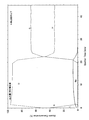
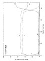
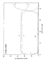
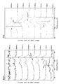
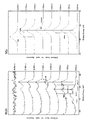
- FIG. 1 It is a depth profile which shows the result of having analyzed the depth direction about the light semipermeable membrane produced in Comparative Example 1 by XPS (X-ray photoelectron spectroscopic analysis: X-ray photoelectron spectroscopy). It is a depth profile which shows the result of having analyzed the depth direction by XPS about the light semipermeable membrane produced in Example 1.
- FIG. 1 X-ray photoelectron spectroscopic analysis: X-ray photoelectron spectroscopy
- Mo molybdenum
- Si silicon
- He argon
- nitrogen nitrogen
- He helium
- FIG. 3 shows the result of XPS (X-ray photoelectron spectroscopy) analysis of this MoSiN film. From FIG.
- the composition of this MoSiN film was Mo: 1.8 atomic%, Si: 53.1 atomic%, and N: 45.1 atomic%.
- the ArF excimer laser irradiation resistance of the light semitransmissive film (MoSiN film) produced in Example 1 was examined. Specifically, with respect to the light translucent film produced in Example 1, an ArF excimer laser (wavelength 193 nm) with a pulse frequency of 300 Hz and a pulse energy of 16 mJ / cm 2 / pulse was continuously applied so as to obtain an integrated dose of 30 kJ / cm 2. Irradiated.
- the irradiation amount of 30 kJ / cm 2 corresponds to the irradiation amount received when the transfer pattern is exposed and transferred to the resist film of 112,500 wafers using the transfer mask. Then, when the film thickness change amount ⁇ d (nm) before and after ArF irradiation was obtained by measurement, it was surprisingly found that the film thickness change amount ⁇ d was 0 nm, and extremely high ArF irradiation resistance was obtained. In addition, the light semi-transmissive film (MoSiN film) after ArF irradiation has a transmittance of 6.7% and a phase difference of 174.9 degrees at the wavelength of ArF excimer laser (193 nm). The change was small.
- Mo molybdenum
- Si silicon
- a mixed gas atmosphere gas flow rate Ar
- Ar argon
- He helium
- This MoSi film had a transmittance of 0% and a phase difference with a transmittance of 0% at the wavelength of ArF excimer laser (193 nm), and could not be measured.
- the results of XPS analysis of this MoSi film are shown in FIG. From FIG. 2, the composition of this MoSi film was Mo: 6.4 atomic% and Si: 93.6 atomic%.
- the ArF irradiation resistance of the light semitransmissive film (MoSi film) produced in Comparative Example 1 was examined in the same manner as in Example 1. As a result, the film thickness variation ⁇ d before and after ArF irradiation was 11.3 nm, far exceeding 4 nm of the pass line.
- Mo molybdenum
- Si silicon
- He helium
- FIG. 4 shows the result of XPS analysis of this MoSiN film. From FIG.
- the composition of this MoSiN film was Mo: 1.3 atomic%, Si: 50.2 atomic%, and N: 48.5 atomic%.
- the ArF irradiation resistance of the light semitransmissive film produced in Comparative Example 2 was examined in the same manner as in Example 1.
- the film thickness change amount ⁇ d before and after ArF irradiation was 4.7 nm, exceeding 4 nm of the pass line.
- the light semi-transmissive film (MoSiN film) after ArF irradiation has a transmittance of 11.0% and a phase difference of 169.4 degrees at the wavelength of ArF excimer laser (193 nm). There was considerable change.
- Example 1 and Comparative Example 2 are compared, the composition of the MoSiN film is approximate and the difference is small. Surprisingly, however, the film thickness change ⁇ d before and after ArF irradiation and the change in transmittance and phase difference before and after ArF irradiation are greatly different. This is presumably due to the difference between whether the MoSiN film is a complete nitride film or an incomplete nitride film. Further, details are considered as follows. In Example 1 and Comparative Example 2, both the contents of Si and N are basically similar, and therefore, the main bonding state in the film is considered to have a high proportion of Si—N bonds. .
- Example 1 and Comparative Example 2 when Example 1 and Comparative Example 2 are compared, in Example 1 and Comparative Example 2, the content of Mo is basically small, and therefore the content of Mo—Si bond and Mo—N bond is also low. small.
- the state of the complete nitride film shown in FIG. 7 is changed to the state of the incomplete nitride film shown in FIG. 6, as shown in the diagram on the left side of FIG. From the state where Mo—N bonds are relatively contained (see 9.00 min and 33.00 min), as shown in the left figure of FIG. 6, there are relatively more Mo—Si bonds than Mo—N bonds. Changes to the included state (see 1.50min, 21.00min).
- the Mo content is basically small as described above may cause a large difference in ArF irradiation resistance.
- the Mo—N bond is relatively larger than the Mo—Si bond shown in the left diagram of FIG. 7, the left diagram of FIG. Since there are relatively few Mo—N bonds, it is considered that the effect of oxidation of MoN (that is, a decrease in light resistance) may be reduced.
- the state of the complete nitride film shown in FIG. 4 is changed to the state of the incomplete nitride film shown in FIG. 3 under the basic state described above, the nitrogen content in the film is reduced by about 3 atomic%.
- the Si content increases by about 3 atomic%.
- the ratio of the nitrogen content in the film to the Si content in the film decreased from about 97% to about 85%.
- a large difference in ArF irradiation resistance is caused by these things and, for example, a difference in bonding state (for example, bonding strength) and film quality due to these factors.
- FIG. 1 shows the relationship between the N 2 gas flow rate (sccm) and the film thickness change ⁇ d (nm) before and after ArF irradiation for the light semi-transmissive films produced in Example 1, Comparative Example 1, and Comparative Example 2. It is a figure which shows a result. From FIG. 1, when performing sputtering in an atmosphere containing nitrogen, an incomplete nitride film is obtained by setting the flow rate of nitrogen in the atmosphere to a flow rate lower than the flow rate for completely nitriding the transition metal and silicon.
- the change amount ⁇ d in film thickness before and after ArF irradiation is 0 nm, and it can be seen that extremely high ArF irradiation resistance can be obtained as compared with the case of a complete nitride film.
- Gas atmosphere gas flow rate Ar: 12.5 sccm, N 2 : 50 sccm, He: 100 sccm), gas pressure 0.3 Pa, DC power supply power 3.0 kW, reactive sputtering (DC sputtering), molybdenum, silicon and A MoSiN film made of nitrogen was formed to a thickness of 67 nm.
- This MoSiN film had a transmittance of 4.8% and a phase difference of 173.9 degrees at the wavelength of ArF excimer laser (193 nm).
- the substrate was heated (annealed) at 500 ° C. for 30 minutes in the air.
- This MoSiN film had a transmittance of 6.1% and a phase difference of 177.3 degrees at the wavelength of ArF excimer laser (193 nm).
- the light transflective film (MoSiN film) produced in Example 2 was examined for ArF irradiation resistance in the same manner as in Example 1. As a result, the film thickness variation ⁇ d before and after ArF irradiation was 2 nm, and it was found that extremely high ArF irradiation resistance was obtained.
- the light transflective film (MoSiN film) after ArF irradiation has a transmittance of 6.8% and a phase difference of 172.1 degrees at the wavelength of ArF excimer laser (193 nm). The change was small.
- Example 3 (Comparative Example 3)
- the target ratio of molybdenum and silicon and the gas flow rate were changed, and the film thickness was 69 nm.
- This MoSiN film had a transmittance of 6.1% and a phase difference of 179.2 degrees at the wavelength of ArF excimer laser (193 nm).
- the light translucent film (MoSiN film) produced in Comparative Example 3 was examined for ArF irradiation resistance in the same manner as in Example 1. As a result, the film thickness variation ⁇ d before and after ArF irradiation was 10 nm, far exceeding 4 nm of the acceptable line.
- the light transflective film (MoSiN film) after ArF irradiation has a transmittance of 7.0% and a phase difference of 170.4 degrees at the wavelength of ArF excimer laser (193 nm). There was considerable change.
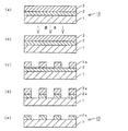
- FIG. 9 is a cross-sectional view showing a process of manufacturing a phase shift mask using a phase shift mask blank.
- a chemically amplified positive resist film for electron beam drawing PRL009 manufactured by Fuji Film Electronics Materials Co., Ltd.
- PRL009 manufactured by Fuji Film Electronics Materials Co., Ltd.
- the resist film 3 was formed by spin coating using a spinner (rotary coating apparatus).
- a desired pattern was drawn on the resist film 3 formed on the mask blank 10 using an electron beam drawing apparatus, and then developed with a predetermined developer to form a resist pattern 3a (see FIG. (See (b) and (c)).
- the resist pattern 3a was etched to form the light semi-transmissive film pattern 2a (see FIG. 4D).
- a mixed gas of SF 6 and He was used as the dry etching gas.
- the remaining resist pattern was peeled off to obtain the phase shift mask 20 (see FIG. 5E).
- the composition, transmittance, and phase difference of the light semi-transmissive film were almost the same as those at the time of manufacturing the mask blank.
- Example 1 when the ArF excimer laser irradiation resistance of the light semi-transmissive film (MoSiN film) pattern of the manufactured phase shift mask was examined, the film thickness change ⁇ d was 0 nm, and the ArF excimer laser was extremely high. It was found that irradiation resistance was obtained. Further, the light transflective film (MoSiN film) after ArF irradiation had a small change in transmittance and phase difference before and after ArF irradiation at the wavelength of ArF excimer laser (193 nm), as in Example 1.
- Example 4 A halftone having a light-shielding band is formed by forming a Cr-based light-shielding film on the light-semitransmissive film manufactured in the same procedure as in Example 1, and patterning each of the Cr-based light-shielding film and the light-semitransmissive film.
- a mold phase shift mask was fabricated.
- the halftone phase shift mask was irradiated with ArF excimer laser (wavelength 193 nm) under the same conditions as in Example 1. Using the prepared halftone phase shift mask, a step of exposing and transferring the transfer pattern to the resist film on the semiconductor wafer, which is a transfer target, was performed.
- an immersion type apparatus using annular illumination using an ArF excimer laser as a light source was used.
- a halftone phase shift mask was set on the mask stage of the exposure apparatus, and exposure transfer was performed on the resist film for ArF immersion exposure on the semiconductor wafer.
- the resist film after the exposure was subjected to a predetermined development process to form a resist pattern.
- a circuit pattern including a line & space (L & S) pattern having a DRAM half pitch (hp) of 32 nm was formed on the semiconductor wafer using the resist pattern.
Landscapes
- Chemical & Material Sciences (AREA)
- Physics & Mathematics (AREA)
- General Physics & Mathematics (AREA)
- Chemical Kinetics & Catalysis (AREA)
- Engineering & Computer Science (AREA)
- Materials Engineering (AREA)
- Mechanical Engineering (AREA)
- Metallurgy (AREA)
- Organic Chemistry (AREA)
- Preparing Plates And Mask In Photomechanical Process (AREA)
- Exposure And Positioning Against Photoresist Photosensitive Materials (AREA)
- Physical Vapour Deposition (AREA)
Abstract
Description
(構成1)
ArFエキシマレーザー露光光が適用される位相シフトマスクを作製するために用いられる位相シフトマスクブランクであって、
透光性基板上に、光半透過膜を備え、
前記光半透過膜は、遷移金属、ケイ素及び窒素を主成分とする不完全窒化物膜からなり、
前記光半透過膜の遷移金属とケイ素との間における遷移金属の含有比率が9%未満であることを特徴とする位相シフトマスクブランク。
(構成2)
前記光半透過膜の遷移金属とケイ素との間における遷移金属の含有比率が2%以上であることを特徴とする構成1記載の位相シフトマスクブランク。
(構成3)
前記不完全窒化膜は、Mo-N結合及びMo-Si結合を含み、Mo-Si結合がMo-N結合よりも相対的に多く含むことを特徴とする構成1又は2記載の位相シフトマスクブランク。
(構成4)
前記不完全窒化膜は、Si-N結合及びMo-Si結合を主として含むことを特徴とする構成1から3のいずれかに記載の位相シフトマスクブランク。
(構成5)
前記光半透過膜の前記露光光の波長に対する透過率が4%以上9%未満であることを特徴とする構成1から3のいずれかに記載の位相シフトマスクブランク。
(構成6)
前記光半透過膜の窒素の含有量は、40原子%以上47原子%以下であることを特徴とする構成1から5のいずれかに記載の位相シフトマスクブランク。
(構成7)
前記遷移金属は、モリブデンであることを特徴とする構成1から6のいずれかに記載の位相シフトマスクブランク。
(構成8)
前記光半透過膜の膜厚は、75nm以下であることを特徴とする構成1から7のいずれかに記載の位相シフトマスクブランク。
(構成9)
ArFエキシマレーザー露光光が適用される位相シフトマスクを作製するために用いられる位相シフトマスクであって、
透光性基板上に、光半透過膜パターンを備え、
前記光半透過膜パターンは、遷移金属、ケイ素及び窒素を主成分とする不完全窒化物膜からなり、
前記光半透過膜パターンにおける遷移金属とケイ素との間における遷移金属の含有比率が9%未満であることを特徴とする位相シフトマスク。
(構成10)
前記光半透過膜パターンにおける遷移金属とケイ素との間における遷移金属の含有比率が2%以上であることを特徴とする構成9記載の位相シフトマスク。
(構成11)
前記不完全窒化膜は、Mo-N結合及びMo-Si結合を含み、Mo-Si結合がMo-N結合よりも相対的に多く含むことを特徴とする構成9又は10記載の位相シフトマスク。
(構成12)
前記不完全窒化膜は、Si-N結合及びMo-Si結合を主として含むことを特徴とする構成9から11のいずれかに記載の位相シフトマスク。
(構成13)
前記光半透過膜パターンにおける窒素の含有量は、40原子%以上47原子%以下であることを特徴とする構成9から12のいずれかに記載の位相シフトマスク。
(構成14)
前記遷移金属は、モリブデンであることを特徴とする構成9から13のいずれかに記載の位相シフトマスク。
(構成15)
前記光半透過膜パターンの膜厚は、75nm以下であることを特徴とする構成9から14のいずれかに記載の位相シフトマスク。
(構成16)
ArFエキシマレーザー露光光が適用される位相シフトマスクを作製するために用いられる位相シフトマスクブランクの製造方法であって、
窒素ガスを含む雰囲気中でスパッタリングを行うことによって、透光性基板上に、遷移金属、ケイ素及び窒素を主成分とする光半透過膜を成膜する工程を備え、
前記雰囲気中の窒素ガスの流量は、前記遷移金属及びケイ素を完全に窒化する流量よりも少ない流量であることを特徴とする位相シフトマスクブランクの製造方法。
(構成17)
前記雰囲気中の窒素ガスの流量は、前記遷移金属及びケイ素を完全に窒化する流量に対して、70%を超え95%未満の流量であることを特徴とする構成16記載の位相シフトマスクブランクの製造方法。
(構成18)
構成1記載の位相シフトマスクブランクを用いて製造された転写用マスクを用い、半導体ウェハ上に回路パターンを形成することを特徴する半導体デバイスの製造方法。
(構成19)
構成9記載の位相シフトマスクを用い、半導体ウェハ上に回路パターンを形成することを特徴する半導体デバイスの製造方法。
透光性基板上に、光半透過膜を備え、
前記光半透過膜は、遷移金属、ケイ素及び窒素を主成分とする不完全窒化物膜からなり、
前記光半透過膜の遷移金属とケイ素との間における遷移金属の含有比率が9%未満であることを特徴とする位相シフトマスクブランクである。
本発明において、不完全窒化物は、完全窒化物に比べ、M-N結合及びSi-N結合が少ない状態にある化合物である、と言える。
例えば、窒素を含む雰囲気中でスパッタリングを行うことによって、透光性基板上に、遷移金属、ケイ素及び窒素を主成分とする光半透過膜を成膜する際に、窒素ガスの流量を増やしていくと、膜中の窒素含有量が増加していく(透過率が上昇していく)が、窒素ガスの流量増加量に対する透過率の上昇量は次第に小さくなっていき、窒素ガスの流量を増やしても、膜中の窒素含有量が増加しない(透過率が上昇しない)状態に至る。本発明においては、この状態を、完全窒化物と称す。また、この完全窒化物の状態に至る手前の状態、即ち、上述した、窒素ガスの流量を増やしても、膜中の窒素含有量が増加する余地のある状態(透過率が上昇する余地のある状態)、を不完全窒化物と称す。不完全窒化物は、上述した、窒素ガスの流量増加に対する透過率の上昇が次第に小さくなっていく状態に含まれる。不完全窒化物は、上述した、窒素ガスの流量増加に対する透過率の上昇が次第に小さくなっていく状態よりも手前の状態は含まない。
すなわち、窒素流量がゼロ(0sccm)の場合(MoSi膜の場合)には、図5に示すように、膜中の主たる結合状態は、Si-Si結合、Mo-Si結合となる。Si-Si結合が多く含まれているので、Siの酸化による耐光性への影響が生じると考えられる。
窒素流量が35sccm未満(ArとN2の合計量に対するN2比率[N2/(Ar+N2)]が77%未満)で窒化が少ない場合には、膜中の主たる結合状態は、Si-Si結合、Si-N結合、Mo-Si結合となる(図5、及び後述する図6参照)。Si-Si結合が多く含まれているので、Siの酸化による耐光性への影響が生じると考えられる。
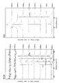
窒素流量が35sccm以上50sccm以下([N2/(Ar+N2)]が77%以上83%以下)の場合には、図6に示すように、膜中の主たる結合状態は、Si-N結合、Mo-Si結合となる。Si-Si結合及びMo-N結合がほとんどないため、Si及びMoが酸化されにくい。詳しくは、図6の左側の図に示すように、Mo-N結合よりもMo-Si結合が相対的に多く含まれているので(1.50min、21.00min参照)、Mo-Si結合よりもMo-N結合が相対的に多く含まれている場合に比べ、Mo-N結合が相対的に少ないため、Moの酸化による影響(即ち耐光性の低下)が小さいと考えられる。
より詳しくは、図6において、束縛エネルギー227.5eV付近のピークが束縛エネルギー228eV付近のピークよりも相対的に高くなっている。ここで、「相対的に高い」とは、膜厚方向に複数ポイント(例えば、5点)測定したときに総合的にみてピークが高いものを含む。
窒素流量が50sccm([N2/(Ar+N2)]が83%)より多い完全窒化膜の場合には、図7に示すように、膜中の主たる結合状態は、Si-N結合、Mo-N結合となる。Mo-N結合が含まれているので、Moが酸化されてしまう。詳しくは、図7の左側の図に示すように、Mo-Si結合よりもMo-N結合が相対的に多く含まれているので(9.00min、33.00min参照)、Mo-N結合よりもMo-Si結合が相対的に多く含まれている場合に比べ、Mo-N結合が相対的に多く含まれているため、Moの酸化による影響(即ち耐光性の低下)が大きいと考えられる。
より詳しくは、図7において、束縛エネルギー227.5eV付近のピークが束縛エネルギー228eV付近のピークよりも相対的に低くなっている。ここで、「相対的に低い」とは、膜厚方向に複数ポイント(例えば、6点)測定したときに総合的にみてピークが低いものを含む。
本発明において、前記光半透過膜の遷移金属Mとケイ素Siとの間における遷移金属Mの含有比率[M/(M+Si)]は、膜中のMo含有量をより少なくし、Mo-N結合をより少なくする観点(耐光性をより向上させる観点)から、7%未満、5%未満であることがより好ましい。
本発明においては、パルス周波数300Hz、パルスエネルギー16mJ/cm2/pulseのArFエキシマレーザー(波長193nm)を積算照射量30kJ/cm2となるように連続照射した場合の膜厚変化量を4nm以下とすることができる。
半導体デバイスの設計仕様でいうDRAM ハーフピッチ(hp)32nm世代ではウェハ上でCDバラツキを2.6nm以下とする必要があり、このためには、hp32nm世代で使用する位相シフトマスクに求められるCDバラツキは5nm以下に抑えることが好ましいが、本発明によれば、位相シフトマスクを作製したときに、薄膜パターンのCDバラツキを5nm以下とすることができる。
本発明においては、前記光半透過膜は、透過率制御のため、20原子%以下の酸素を入れることが可能である。
本発明において、遷移金属Mとしては、モリブデン、タンタル、タングステン、チタン、クロム、ハフニウム、ニッケル、バナジウム、ジルコニウム、ルテニウム、ロジウム等が適用可能である。
このような構成により、欠陥検査機の検査光の波長(例えば、257nm)に対する透過率を60%以下とすることが可能となる。また、光半透過膜の薄膜化が可能となる。
本発明において、前記光半透過膜の遷移金属Mとケイ素Siとの間における遷移金属Mの含有比率[M/(M+Si)]は、より好ましくは3%以上である。
前記透過率が9%より大きいと、不完全窒化の状態が得られ難くなり、上述した作用効果が得られ難くなる。詳しくは、前記透過率が9%より大きいと、窒素ガス流量をゼロ付近に小さくしても完全窒化の状態になってしまう(したがって不完全窒化の状態が得られない)。前記透過率のより好ましい範囲は8%以下である。前記透過率が4%より低いと膜厚が厚くなる。
ここでの透過率は、アニール等を行わない成膜後のものをいう。したがって、応力低減等でアニールする場合には、アニールによる透過率変動を見越して成膜することが必要である。
図6に示すように、膜中の結合状態において、Mo-Si結合がMo-N結合よりも相対的に多いため、Si及びMoが酸化されにくく、耐光性が高くなるので好ましいためである。
本発明において、前記不完全窒化膜は、Si-N結合及びMo-Si結合を主として含むことが好ましい(構成4)。
図6に示すように、膜中の主たる結合状態がSi-N結合、Mo-Si結合となる場合においては、Si-Si結合及びMo-N結合がほとんどないため、Si及びMoが酸化されにくく、耐光性が高くなるので好ましいためである。
なお、上記膜中の主たる結合状態は、アニール等で酸化層等が形成される表層部分は除く部分に関するものである。
膜中のMo含有量や透過率等との関係で一概に言えないが、前記光半透過膜の窒素の含有量が47原子%を超えると、不完全窒化の状態が得られ難くなる。前記光半透過膜の窒素の含有量が40原子%より少ないとSi-Si結合が多くなり耐光性が悪くなる傾向にある。
本発明において、完全窒化物の光半透過膜における窒素含有量に対して、2%以上20%以下窒素の含有量が少ないことが好ましい。光半透過膜の窒素の含有量が完全窒化物の光半透過膜における窒素含有量に対して2%未満の場合には、不完全窒化の状態が得られ難くなる。また、完全窒化物の光半透過膜における窒素含有量に対して、20%を超えて少ないと、Si-Si結合が多くなり耐光性が悪くなる傾向にある。
前記遷移金属がモリブデンである場合に、本願課題が特に顕著になるからである。
前記光半透過膜の膜厚は、70nm以下であることがさらに好ましい。
前記雰囲気中の窒素ガスの流量は、前記遷移金属及びケイ素を完全に窒化する流量よりも少ない流量であることを特徴とする。
このような構成によれば、不完全窒化の状態にある遷移金属、ケイ素及び窒素を主成分とする光半透過膜を成膜可能となる。
本発明において、前記雰囲気中の窒素ガスの流量は、前記遷移金属及びケイ素を完全に窒化する流量に対して、70%を超え95%未満の流量であることが好ましい(構成17)。
このような構成によれば、安定的に確実に再現性よく不完全窒化の状態にある遷移金属、ケイ素及び窒素を主成分とする光半透過膜を成膜できる。それにより、後述する条件におけるArFエキシマレーザー照射前後の膜厚変化量Δdが4nm以下であって、完全窒化の状態にある光半透過膜に比べ、耐光性に優れた光半透過膜を成膜できる。
スパッタ装置としてDCマグネトロンスパッタ装置が好ましく挙げられるが、本発明はこの成膜装置に限定されるわけではない。RFマグネトロンスパッタ装置等、他の方式のスパッタ装置を使用してもよい。
本発明において、位相シフトマスクブランクには、ハーフトーン型位相シフトマスク用のマスクブランクが含まれる。
例えば、前記光半透過膜の上又は下に遮光膜を有する形態の場合には、前記光半透過膜の材料が遷移金属シリサイドを含むので、遮光膜の材料は、前記光半透過膜に対してエッチング選択性を有する(エッチング耐性を有する)クロムや、クロムに酸素、窒素、炭素などの元素を添加したクロム化合物で構成することができる。これにより、光半透過膜パターンの上又は下に遮光膜パターンを形成できる。
本発明において、クロムを含有する材料としては、クロム単体(Cr)の他、クロム(Cr)に窒素(N)、酸素(O)、炭素(C)、水素(H)、ヘリウム(He)などの元素を一以上含有する材料が含まれる。例えば、Cr、CrN、CrO、CrNO、CrNC、CrCONなどや、これらに加え水素(H)、ヘリウム(He)をそれぞれ含有する材料が含まれる。
(実施例1)
図8に示すように、透光性基板1としてサイズ6インチ角、厚さ0.25インチの合成石英ガラス基板を用い、透光性基板1上に、窒化されたモリブデン及びシリコンからなる光半透過膜2を成膜した。
具体的には、モリブデン(Mo)とシリコン(Si)との混合ターゲット(Mo:Si=4mol%:96mol%)を用い、アルゴン(Ar)と窒素(N2)とヘリウム(He)との混合ガス雰囲気(ガス流量 Ar:10.5sccm、N2:48sccm、He:100sccm)、ガス圧0.3Pa、DC電源の電力を3.0kWとして、反応性スパッタリング(DCスパッタリング)により、モリブデン、シリコン及び窒素からなるMoSiN膜を67nmの膜厚で形成した。
このMoSiN膜は、ArFエキシマレーザーの波長(193nm)において、透過率は6.2%、位相差が180.0度となっていた。
以上のようにして、本実施例の位相シフトマスクブランク10を作製した。
このMoSiN膜について、XPS(X線光電子分光法)分析した結果を図3に示す。図3から、このMoSiN膜の組成は、Mo:1.8原子%,Si:53.1原子%,N:45.1原子%であった。
次に、実施例1で作製した光半透過膜(MoSiN膜)について、ArFエキシマレーザー照射耐性を調べた。具体的には、実施例1で作製した光半透過膜について、パルス周波数300Hz、パルスエネルギー16mJ/cm2/pulseのArFエキシマレーザー(波長193nm)を積算照射量30kJ/cm2となるように連続照射した。ここで、照射量30kJ/cm2というのは、転写用マスクを用いて、ウェハ112,500枚のレジスト膜に対して、転写パターンを露光転写したときに受ける照射量に相当する。
そして、ArF照射前後における膜厚変化量Δd(nm)を測定により求めたところ、驚くべきことに、膜厚変化量Δdは0nmであり、極めて高いArF照射耐性が得られることがわかった。
また、ArF照射後における光半透過膜(MoSiN膜)は、ArFエキシマレーザーの波長(193nm)において、透過率は6.7%、位相差が174.9度となっており、ArF照射前後で変化は小さかった。
実施例1において、窒素(N2)の流量を0sccmとし、膜厚を54nmとしたこと、を除き実施例1と同様とした。
具体的には、モリブデン(Mo)とシリコン(Si)との混合ターゲット(Mo:Si=4mol%:96mol%)を用い、アルゴン(Ar)とヘリウム(He)との混合ガス雰囲気(ガス流量 Ar:10.5sccm、He:100sccm)、ガス圧0.3Pa、DC電源の電力を3.0kWとして、スパッタリング(DCスパッタリング)により、モリブデン及びシリコンからなるMoSi膜を54nmの膜厚で透光性基板上に形成した。
このMoSi膜は、ArFエキシマレーザーの波長(193nm)において、透過率は0%、位相差は透過率が小さく測定不可能であった。
このMoSi膜について、XPS分析した結果を図2に示す。図2から、このMoSi膜の組成は、Mo:6.4原子%,Si:93.6原子%であった。
次に、比較例1で作製した光半透過膜(MoSi膜)について、実施例1と同様にしてArF照射耐性を調べた。その結果、ArF照射前後における膜厚変化量Δdは、11.3nmであり、合格ラインの4nmをはるかに超えていた。
実施例1において、窒素(N2)の流量を55sccmとしたこと、を除き実施例1と同様とした。
具体的には、モリブデン(Mo)とシリコン(Si)との混合ターゲット(Mo:Si=4mol%:96mol%)を用い、アルゴン(Ar)と窒素(N2)とヘリウム(He)との混合ガス雰囲気(ガス流量 Ar:10.5sccm、N2:55sccm、He:100sccm)、ガス圧0.3Pa、DC電源の電力を3.0kWとして、反応性スパッタリング(DCスパッタリング)により、モリブデン、シリコン及び窒素からなるMoSiN膜を67nmの膜厚で透光性基板上に形成した。
このMoSiN膜は、ArFエキシマレーザーの波長(193nm)において、透過率は9.6%、位相差が178.2度となっていた。
このMoSiN膜について、XPS分析した結果を図4に示す。図4から、このMoSiN膜の組成は、Mo:1.3原子%,Si:50.2原子%,N:48.5原子%であった。
次に、比較例2で作製した光半透過膜について、実施例1と同様にしてArF照射耐性を調べた。その結果、ArF照射前後における膜厚変化量Δdは、4.7nmであり、合格ラインの4nmを超えていた。
また、ArF照射後における光半透過膜(MoSiN膜)は、ArFエキシマレーザーの波長(193nm)において、透過率は11.0%、位相差が169.4度となっており、ArF照射前後で変化がかなりあった。
また、詳しくは、以下のように考えられる。
実施例1及び比較例2では、基本的に、共に、SiとNの含有量が近似しており、したがって、膜中の主たる結合状態は、Si-N結合の占める割合が高いものと考えられる。 また、実施例1と比較例2を対比すると、実施例1及び比較例2では、基本的に、共に、Moの含有量が小さく、したがって、Mo-Si結合、Mo-N結合の含有量も小さい。
以上の基本的な状態の下で、図7に示す完全窒化膜の状態から図6に示す不完全窒化膜の状態になると、図7の左側の図に示すように、Mo-Si結合よりもMo-N結合が相対的に多く含まれている(9.00min、33.00min参照)状態から、図6の左側の図に示すように、Mo-N結合よりもMo-Si結合が相対的に多く含まれている(1.50min、21.00min参照)状態へと変化する。これらのことと、上述したように基本的にMoの含有量が小さいこと、が相まって、ArF照射耐性に大きな違いが生ずるのではないかと考えられる。例えば、図7の左側の図に示すMo-Si結合よりもMo-N結合が相対的に多く含まれている場合に比べ、図6の左側の図では、Mo-Si結合が相対的に多くMo-N結合が相対的に少ないため、MoNの酸化による影響(即ち耐光性の低下)が小さくなるのではないかと考えられる。
また、上述した基本的な状態の下で、図4に示す完全窒化膜の状態から図3に示す不完全窒化膜の状態になると、膜中の窒素の含有量が約3原子%減り、膜中のSiの含有量が約3原子%増える。これに伴い、膜中のSiの含有量に対する膜中の窒素の含有量の割合(膜中の窒素の含有量/膜中のSiの含有量)は、約97%から約85%へと低下する。これらのことや、これらのことに起因して例えば結合の状態(例えば結合の強さ)や膜質などに違いが生じること、によってArF照射耐性に大きな違いが生ずるのではないかと考えられる。
図1から、窒素を含む雰囲気中でスパッタリングを行う際に、雰囲気中の窒素の流量は、遷移金属及びケイ素を完全に窒化する流量よりも少ない流量とすることによって、不完全窒化膜を得ることができ、この結果、ArF照射前後における膜厚変化量Δdは0nmであり、完全窒化膜の場合に比べ、極めて高いArF照射耐性が得られることがわかる。
実施例1において、モリブデンとシリコンのターゲット比率及びガス流量を変え、膜厚を67nmとした。
具体的には、モリブデン(Mo)とシリコン(Si)との混合ターゲット(Mo:Si=6mol%:94mol%)を用い、アルゴン(Ar)と窒素(N2)とヘリウム(He)との混合ガス雰囲気(ガス流量 Ar:12.5sccm、N2:50sccm、He:100sccm)、ガス圧0.3Pa、DC電源の電力を3.0kWとして、反応性スパッタリング(DCスパッタリング)により、モリブデン、シリコン及び窒素からなるMoSiN膜を67nmの膜厚で形成した。
このMoSiN膜は、ArFエキシマレーザーの波長(193nm)において、透過率は4.8%、位相差が173.9度となっていた。
次に、上記基板を大気中で500℃で30分間加熱処理(アニール処理)した。このMoSiN膜は、ArFエキシマレーザーの波長(193nm)において、透過率は6.1%、位相差が177.3度となっていた。
実施例2で作製した光半透過膜(MoSiN膜)について、実施例1と同様にしてArF照射耐性を調べた。その結果、ArF照射前後における膜厚変化量Δdは、2nmであり、極めて高いArF照射耐性が得られることがわかった。
また、ArF照射後における光半透過膜(MoSiN膜)は、ArFエキシマレーザーの波長(193nm)において、透過率は6.8%、位相差が172.1度となっており、ArF照射前後で変化は小さかった。
実施例1において、モリブデンとシリコンのターゲット比率及びガス流量を変え、膜厚を69nmとした。
具体的には、モリブデン(Mo)とシリコン(Si)との混合ターゲット(Mo:Si=10mol%:90mol%)を用い、アルゴン(Ar)と窒素(N2)とヘリウム(He)との混合ガス雰囲気(ガス流量 Ar:8sccm、N2:72sccm、He:100sccm)、ガス圧0.3Pa、DC電源の電力を3.0kWとして、反応性スパッタリング(DCスパッタリング)により、モリブデン、シリコン及び窒素からなるMoSiN膜を69nmの膜厚で形成した。
このMoSiN膜は、ArFエキシマレーザーの波長(193nm)において、透過率は4.9%、位相差が177.6度となっていた。
次に、上記基板を大気中で280℃で10分間加熱処理(アニール処理)した。このMoSiN膜は、ArFエキシマレーザーの波長(193nm)において、透過率は6.1%、位相差が179.2度となっていた。
比較例3で作製した光半透過膜(MoSiN膜)について、実施例1と同様にしてArF照射耐性を調べた。その結果、ArF照射前後における膜厚変化量Δdは、10nmであり、合格ラインの4nmをはるかに超えていた。
また、ArF照射後における光半透過膜(MoSiN膜)は、ArFエキシマレーザーの波長(193nm)において、透過率は7.0%、位相差が170.4度となっており、ArF照射前後で変化がかなりあった。
上記実施例1と同様の位相シフトマスクブランクを用いてハーフトーン型位相シフトマスクを作製した。図9は、位相シフトマスクブランクを用いて位相シフトマスクを製造する工程を示す断面図である。まず、マスクブランク10上に、レジスト膜3として、電子線描画用化学増幅型ポジレジスト膜(富士フィルムエレクトロニクスマテリアルズ社製 PRL009)を形成した(同図(a)参照)。レジスト膜3の形成は、スピンナー(回転塗布装置)を用いて、回転塗布した。
次に、上記レジストパターン3aをマスクとして、光半透過膜2(MoSiN膜)のエッチングを行って光半透過膜パターン2aを形成した(同図(d)参照)。ドライエッチングガスとして、SF6とHeの混合ガスを用いた。
次に、残存するレジストパターンを剥離して、位相シフトマスク20を得た(同図(e)参照)。なお、光半透過膜の組成、透過率、位相差はマスクブランク製造時と殆ど変化はなかった。
実施例1と同様に、作製された位相シフトマスクの光半透過膜(MoSiN膜)パターンについて、ArFエキシマレーザー照射耐性を調べたところ、膜厚変化量Δdは0nmであり、極めて高いArFエキシマレーザー照射耐性が得られることがわかった。
また、ArF照射後における光半透過膜(MoSiN膜)は、ArFエキシマレーザーの波長(193nm)において、実施例1と同様に、透過率及び位相差は、ArF照射前後で変化は小さかった。
実施例1と同様の手順で作製された光半透過膜上に、Cr系遮光膜を成膜し、該Cr系遮光膜及び光半透過膜を各々パターニングすることにより、遮光帯を有するハーフトーン型位相シフトマスクを作製した。このハーフトーン型位相シフトマスクに対し、ArFエキシマレーザー(波長193nm)の照射を実施例1と同じ条件で行った。この準備したハーフトーン型位相シフトマスクを用いて、転写対象物である半導体ウェハ上のレジスト膜に対して、転写パターンを露光転写する工程を行った。露光装置には、ArFエキシマレーザーを光源とする輪帯照明(Annular Illumination)が用いられた液浸方式のものが用いられた。具体的には、露光装置のマスクステージに、ハーフトーン型位相シフトマスクをセットし、半導体ウェハ上のArF液浸露光用のレジスト膜に対して、露光転写を行った。露光後のレジスト膜に対して、所定の現像処理を行い、レジストパターンを形成した。
さらに、レジストパターンを用いて、半導体ウェハ上に、DRAMハーフピッチ(hp)32nmのライン&スペース(L&S)パターンを含む回路パターンを形成した。
Claims (19)
- ArFエキシマレーザー露光光が適用される位相シフトマスクを作製するために用いられる位相シフトマスクブランクであって、
透光性基板上に、光半透過膜を備え、
前記光半透過膜は、遷移金属、ケイ素及び窒素を主成分とする不完全窒化物膜からなり、
前記光半透過膜の遷移金属とケイ素との間における遷移金属の含有比率が9%未満であることを特徴とする位相シフトマスクブランク。 - 前記光半透過膜の遷移金属とケイ素との間における遷移金属の含有比率が2%以上であることを特徴とする請求項1記載の位相シフトマスクブランク。
- 前記不完全窒化膜は、Mo-N結合及びMo-Si結合を含み、Mo-Si結合がMo-N結合よりも相対的に多く含むことを特徴とする請求項1又は2記載の位相シフトマスクブランク。
- 前記不完全窒化膜は、Si-N結合及びMo-Si結合を主として含むことを特徴とする請求項1から3のいずれかに記載の位相シフトマスクブランク。
- 前記光半透過膜の前記露光光の波長に対する透過率が4%以上9%未満であることを特徴とする請求項1から3のいずれかに記載の位相シフトマスクブランク。
- 前記光半透過膜の窒素の含有量は、40原子%以上47原子%以下であることを特徴とする請求項1から5のいずれかに記載の位相シフトマスクブランク。
- 前記遷移金属は、モリブデンであることを特徴とする請求項1から6のいずれかに記載の位相シフトマスクブランク。
- 前記光半透過膜の膜厚は、75nm以下であることを特徴とする請求項1から7のいずれかに記載の位相シフトマスクブランク。
- ArFエキシマレーザー露光光が適用される位相シフトマスクを作製するために用いられる位相シフトマスクであって、
透光性基板上に、光半透過膜パターンを備え、
前記光半透過膜パターンは、遷移金属、ケイ素及び窒素を主成分とする不完全窒化物膜からなり、
前記光半透過膜パターンにおける遷移金属とケイ素との間における遷移金属の含有比率が9%未満であることを特徴とする位相シフトマスク。 - 前記光半透過膜パターンにおける遷移金属とケイ素との間における遷移金属の含有比率が2%以上であることを特徴とする請求項9記載の位相シフトマスク。
- 前記不完全窒化膜は、Mo-N結合及びMo-Si結合を含み、Mo-Si結合がMo-N結合よりも相対的に多く含むことを特徴とする請求項9又は10記載の位相シフトマスク。
- 前記不完全窒化膜は、Si-N結合及びMo-Si結合を主として含むことを特徴とする請求項9から11のいずれかに記載の位相シフトマスク。
- 前記光半透過膜パターンにおける窒素の含有量は、40原子%以上47原子%以下であることを特徴とする請求項9から12のいずれかに記載の位相シフトマスク。
- 前記遷移金属は、モリブデンであることを特徴とする請求項9から13のいずれかに記載の位相シフトマスク。
- 前記光半透過膜パターンの膜厚は、75nm以下であることを特徴とする請求項9から14のいずれかに記載の位相シフトマスク。
- ArFエキシマレーザー露光光が適用される位相シフトマスクを作製するために用いられる位相シフトマスクブランクの製造方法であって、
窒素ガスを含む雰囲気中でスパッタリングを行うことによって、透光性基板上に、遷移金属、ケイ素及び窒素を主成分とする光半透過膜を成膜する工程を備え、
前記雰囲気中の窒素ガスの流量は、前記遷移金属及びケイ素を完全に窒化する流量よりも少ない流量であることを特徴とする位相シフトマスクブランクの製造方法。 - 前記雰囲気中の窒素ガスの流量は、前記遷移金属及びケイ素を完全に窒化する流量に対して、70%を超え95%未満の流量であることを特徴とする請求項16記載の位相シフトマスクブランクの製造方法。
- 請求項1記載の位相シフトマスクブランクを用いて製造された転写用マスクを用い、半導体ウェハ上に回路パターンを形成することを特徴する半導体デバイスの製造方法。
- 請求項9記載の位相シフトマスクを用い、半導体ウェハ上に回路パターンを形成することを特徴する半導体デバイスの製造方法。
Priority Applications (6)
| Application Number | Priority Date | Filing Date | Title |
|---|---|---|---|
| JP2012509319A JP5313401B2 (ja) | 2010-04-09 | 2011-04-08 | 位相シフトマスクブランク及びその製造方法、並びに位相シフトマスク |
| US13/639,686 US8999609B2 (en) | 2010-04-09 | 2011-04-08 | Phase shift mask blank, method of manufacturing the same, and phase shift mask |
| KR1020127029347A KR102071721B1 (ko) | 2010-04-09 | 2011-04-08 | 위상 시프트 마스크 블랭크 및 그 제조 방법, 및 위상 시프트 마스크 |
| CN201180018078.0A CN102834773B (zh) | 2010-04-09 | 2011-04-08 | 相移掩模坯料及其制造方法、以及相移掩模 |
| KR1020187010644A KR102008857B1 (ko) | 2010-04-09 | 2011-04-08 | 위상 시프트 마스크 블랭크 및 그 제조 방법, 및 위상 시프트 마스크 |
| US14/627,426 US9436079B2 (en) | 2010-04-09 | 2015-02-20 | Phase shift mask blank, method of manufacturing the same, and phase shift mask |
Applications Claiming Priority (2)
| Application Number | Priority Date | Filing Date | Title |
|---|---|---|---|
| JP2010090435 | 2010-04-09 | ||
| JP2010-090435 | 2010-04-09 |
Related Child Applications (2)
| Application Number | Title | Priority Date | Filing Date |
|---|---|---|---|
| US13/639,686 A-371-Of-International US8999609B2 (en) | 2010-04-09 | 2011-04-08 | Phase shift mask blank, method of manufacturing the same, and phase shift mask |
| US14/627,426 Division US9436079B2 (en) | 2010-04-09 | 2015-02-20 | Phase shift mask blank, method of manufacturing the same, and phase shift mask |
Publications (1)
| Publication Number | Publication Date |
|---|---|
| WO2011125337A1 true WO2011125337A1 (ja) | 2011-10-13 |
Family
ID=44762306
Family Applications (1)
| Application Number | Title | Priority Date | Filing Date |
|---|---|---|---|
| PCT/JP2011/002090 Ceased WO2011125337A1 (ja) | 2010-04-09 | 2011-04-08 | 位相シフトマスクブランク及びその製造方法、並びに位相シフトマスク |
Country Status (6)
| Country | Link |
|---|---|
| US (2) | US8999609B2 (ja) |
| JP (2) | JP5313401B2 (ja) |
| KR (2) | KR102071721B1 (ja) |
| CN (2) | CN102834773B (ja) |
| TW (2) | TWI519888B (ja) |
| WO (1) | WO2011125337A1 (ja) |
Cited By (11)
| Publication number | Priority date | Publication date | Assignee | Title |
|---|---|---|---|---|
| JP5630592B1 (ja) * | 2013-06-17 | 2014-11-26 | 大日本印刷株式会社 | フォトマスクの製造方法 |
| JP2016021075A (ja) * | 2014-03-18 | 2016-02-04 | Hoya株式会社 | マスクブランク、位相シフトマスクおよび半導体デバイスの製造方法 |
| JP2018017825A (ja) * | 2016-07-26 | 2018-02-01 | アルバック成膜株式会社 | 位相シフタ膜の製造方法、位相シフトマスクブランクの製造方法、及び、位相シフトマスクの製造方法 |
| JP2018054836A (ja) * | 2016-09-28 | 2018-04-05 | 信越化学工業株式会社 | ハーフトーン位相シフトマスクブランク及びハーフトーン位相シフトマスク |
| JP2018109792A (ja) * | 2013-03-19 | 2018-07-12 | Hoya株式会社 | 位相シフトマスクブランク及びその製造方法、位相シフトマスクの製造方法、並びに表示装置の製造方法 |
| JP2020021087A (ja) * | 2016-09-28 | 2020-02-06 | 信越化学工業株式会社 | ハーフトーン位相シフト型フォトマスクブランク及びハーフトーン位相シフト型フォトマスク |
| US20200285144A1 (en) * | 2017-09-21 | 2020-09-10 | Hoya Corporation | Mask blank, transfer mask, and method for manufacturing semiconductor device |
| JP2021170128A (ja) * | 2019-10-01 | 2021-10-28 | 信越化学工業株式会社 | ハーフトーン位相シフト型フォトマスクブランク及びハーフトーン位相シフト型フォトマスク |
| KR20220112182A (ko) | 2021-02-03 | 2022-08-10 | 알박 세이마쿠 가부시키가이샤 | 마스크 블랭크스 및 포토마스크 |
| KR20220112183A (ko) | 2021-02-03 | 2022-08-10 | 알박 세이마쿠 가부시키가이샤 | 마스크 블랭크스 및 포토마스크 |
| KR20220112184A (ko) | 2021-02-03 | 2022-08-10 | 알박 세이마쿠 가부시키가이샤 | 마스크 블랭크스 및 포토마스크 |
Families Citing this family (16)
| Publication number | Priority date | Publication date | Assignee | Title |
|---|---|---|---|---|
| PL2317511T3 (pl) * | 2009-11-03 | 2012-08-31 | Bayer Materialscience Ag | Formulacje fotopolimerowe z nastawialnym mechanicznym modułem Guv |
| KR101300791B1 (ko) * | 2011-12-15 | 2013-08-29 | 한국생산기술연구원 | 전자빔 조사를 이용한 몰리브덴 박막의 전도도 향상 방법 |
| JP5286455B1 (ja) * | 2012-03-23 | 2013-09-11 | Hoya株式会社 | マスクブランク、転写用マスクおよびこれらの製造方法 |
| WO2014073389A1 (ja) | 2012-11-08 | 2014-05-15 | Hoya株式会社 | マスクブランクの製造方法および転写用マスクの製造方法 |
| WO2014112457A1 (ja) * | 2013-01-15 | 2014-07-24 | Hoya株式会社 | マスクブランク、位相シフトマスクおよびこれらの製造方法 |
| JP6364813B2 (ja) * | 2014-02-27 | 2018-08-01 | 大日本印刷株式会社 | フォトマスクの製造方法 |
| US10365556B2 (en) | 2015-03-27 | 2019-07-30 | Hoya Corporation | Mask blank, phase shift mask, method for manufacturing phase shift mask, and method for manufacturing semiconductor device |
| US9897911B2 (en) * | 2015-08-31 | 2018-02-20 | Shin-Etsu Chemical Co., Ltd. | Halftone phase shift photomask blank, making method, and halftone phase shift photomask |
| JP6500791B2 (ja) * | 2016-01-22 | 2019-04-17 | 信越化学工業株式会社 | ハーフトーン位相シフト型フォトマスクブランク及びその製造方法 |
| KR101801101B1 (ko) * | 2016-03-16 | 2017-11-27 | 주식회사 에스앤에스텍 | 위상반전 블랭크 마스크 및 포토 마스크 |
| JP6740349B2 (ja) | 2016-07-19 | 2020-08-12 | Hoya株式会社 | マスクブランク、位相シフトマスク、及び半導体デバイスの製造方法 |
| US11112690B2 (en) * | 2016-08-26 | 2021-09-07 | Hoya Corporation | Mask blank, transfer mask, and method for manufacturing semiconductor device |
| JP6677139B2 (ja) * | 2016-09-28 | 2020-04-08 | 信越化学工業株式会社 | ハーフトーン位相シフト型フォトマスクブランクの製造方法 |
| JP6740107B2 (ja) * | 2016-11-30 | 2020-08-12 | Hoya株式会社 | マスクブランク、転写用マスク及び半導体デバイスの製造方法 |
| CN111512226B (zh) * | 2017-12-26 | 2023-09-26 | Hoya株式会社 | 掩模坯料、相移掩模及半导体器件的制造方法 |
| JP7297692B2 (ja) * | 2019-02-28 | 2023-06-26 | Hoya株式会社 | フォトマスクブランク、フォトマスクの製造方法、および表示装置の製造方法 |
Citations (3)
| Publication number | Priority date | Publication date | Assignee | Title |
|---|---|---|---|---|
| JPH1069064A (ja) * | 1997-07-07 | 1998-03-10 | Hoya Corp | ハーフトーン位相シフトマスクの製造方法 |
| JPH10148929A (ja) * | 1996-03-30 | 1998-06-02 | Hoya Corp | 位相シフトマスク、及び位相シフトマスクブランク |
| JP2002162726A (ja) * | 2000-09-12 | 2002-06-07 | Hoya Corp | 位相シフトマスクブランクの製造方法、及び位相シフトマスクの製造方法 |
Family Cites Families (18)
| Publication number | Priority date | Publication date | Assignee | Title |
|---|---|---|---|---|
| US5415953A (en) * | 1994-02-14 | 1995-05-16 | E. I. Du Pont De Nemours And Company | Photomask blanks comprising transmissive embedded phase shifter |
| JPH1048808A (ja) * | 1996-05-30 | 1998-02-20 | Hoya Corp | フォトマスクの製造方法 |
| JPH11184067A (ja) * | 1997-12-19 | 1999-07-09 | Hoya Corp | 位相シフトマスク及び位相シフトマスクブランク |
| JP2002156742A (ja) | 2000-11-20 | 2002-05-31 | Shin Etsu Chem Co Ltd | 位相シフトマスクブランク、位相シフトマスク及びこれらの製造方法 |
| JP2002258458A (ja) * | 2000-12-26 | 2002-09-11 | Hoya Corp | ハーフトーン型位相シフトマスク及びマスクブランク |
| JP4466805B2 (ja) | 2001-03-01 | 2010-05-26 | 信越化学工業株式会社 | 位相シフトマスクブランク及び位相シフトマスク |
| US20020182893A1 (en) * | 2001-06-05 | 2002-12-05 | International Business Machines Corporation | Oxidation of silicon nitride films in semiconductor devices |
| JP2003215778A (ja) | 2002-01-21 | 2003-07-30 | Shin Etsu Chem Co Ltd | スパッタターゲット、該スパッタターゲットを用いた位相シフトマスクブランク及び位相シフトマスクの製造方法 |
| US6875546B2 (en) * | 2003-03-03 | 2005-04-05 | Freescale Semiconductor, Inc. | Method of patterning photoresist on a wafer using an attenuated phase shift mask |
| JP4535241B2 (ja) * | 2004-03-31 | 2010-09-01 | 凸版印刷株式会社 | ハーフトーン型位相シフトマスク用ブランク、ハーフトーン型位相シフトマスク及びパターン転写方法 |
| JP2005284216A (ja) * | 2004-03-31 | 2005-10-13 | Shin Etsu Chem Co Ltd | 成膜用ターゲット及び位相シフトマスクブランクの製造方法 |
| JP4407815B2 (ja) * | 2004-09-10 | 2010-02-03 | 信越化学工業株式会社 | フォトマスクブランク及びフォトマスク |
| JP2007271661A (ja) * | 2006-03-30 | 2007-10-18 | Hoya Corp | マスクブランク及びハーフトーン型位相シフトマスク |
| JP4958149B2 (ja) * | 2006-11-01 | 2012-06-20 | Hoya株式会社 | 位相シフトマスクブランクの製造方法及び位相シフトマスクの製造方法 |
| JP5702920B2 (ja) * | 2008-06-25 | 2015-04-15 | Hoya株式会社 | 位相シフトマスクブランク、位相シフトマスクおよび位相シフトマスクブランクの製造方法 |
| WO2009157506A1 (ja) * | 2008-06-25 | 2009-12-30 | Hoya株式会社 | 位相シフトマスクブランクおよび位相シフトマスク |
| JP5497288B2 (ja) * | 2008-12-29 | 2014-05-21 | Hoya株式会社 | フォトマスクブランクの製造方法及びフォトマスクの製造方法 |
| US8663876B2 (en) * | 2009-02-13 | 2014-03-04 | Hoya Corporation | Photomask blank, method of manufacturing the same, photomask, and method of manufacturing the same |
-
2011
- 2011-04-08 WO PCT/JP2011/002090 patent/WO2011125337A1/ja not_active Ceased
- 2011-04-08 CN CN201180018078.0A patent/CN102834773B/zh active Active
- 2011-04-08 TW TW100112282A patent/TWI519888B/zh active
- 2011-04-08 US US13/639,686 patent/US8999609B2/en active Active
- 2011-04-08 KR KR1020127029347A patent/KR102071721B1/ko active Active
- 2011-04-08 KR KR1020187010644A patent/KR102008857B1/ko active Active
- 2011-04-08 JP JP2012509319A patent/JP5313401B2/ja active Active
- 2011-04-08 CN CN201610184327.8A patent/CN105739233B/zh active Active
- 2011-04-08 TW TW104141184A patent/TWI588593B/zh active
-
2013
- 2013-07-03 JP JP2013139879A patent/JP5758448B2/ja active Active
-
2015
- 2015-02-20 US US14/627,426 patent/US9436079B2/en active Active
Patent Citations (3)
| Publication number | Priority date | Publication date | Assignee | Title |
|---|---|---|---|---|
| JPH10148929A (ja) * | 1996-03-30 | 1998-06-02 | Hoya Corp | 位相シフトマスク、及び位相シフトマスクブランク |
| JPH1069064A (ja) * | 1997-07-07 | 1998-03-10 | Hoya Corp | ハーフトーン位相シフトマスクの製造方法 |
| JP2002162726A (ja) * | 2000-09-12 | 2002-06-07 | Hoya Corp | 位相シフトマスクブランクの製造方法、及び位相シフトマスクの製造方法 |
Cited By (12)
| Publication number | Priority date | Publication date | Assignee | Title |
|---|---|---|---|---|
| JP2018109792A (ja) * | 2013-03-19 | 2018-07-12 | Hoya株式会社 | 位相シフトマスクブランク及びその製造方法、位相シフトマスクの製造方法、並びに表示装置の製造方法 |
| JP5630592B1 (ja) * | 2013-06-17 | 2014-11-26 | 大日本印刷株式会社 | フォトマスクの製造方法 |
| JP2016021075A (ja) * | 2014-03-18 | 2016-02-04 | Hoya株式会社 | マスクブランク、位相シフトマスクおよび半導体デバイスの製造方法 |
| US10444620B2 (en) | 2014-03-18 | 2019-10-15 | Hoya Corporation | Mask blank, phase-shift mask and method for manufacturing semiconductor device |
| JP2018017825A (ja) * | 2016-07-26 | 2018-02-01 | アルバック成膜株式会社 | 位相シフタ膜の製造方法、位相シフトマスクブランクの製造方法、及び、位相シフトマスクの製造方法 |
| JP2018054836A (ja) * | 2016-09-28 | 2018-04-05 | 信越化学工業株式会社 | ハーフトーン位相シフトマスクブランク及びハーフトーン位相シフトマスク |
| JP2020021087A (ja) * | 2016-09-28 | 2020-02-06 | 信越化学工業株式会社 | ハーフトーン位相シフト型フォトマスクブランク及びハーフトーン位相シフト型フォトマスク |
| US20200285144A1 (en) * | 2017-09-21 | 2020-09-10 | Hoya Corporation | Mask blank, transfer mask, and method for manufacturing semiconductor device |
| JP2021170128A (ja) * | 2019-10-01 | 2021-10-28 | 信越化学工業株式会社 | ハーフトーン位相シフト型フォトマスクブランク及びハーフトーン位相シフト型フォトマスク |
| KR20220112182A (ko) | 2021-02-03 | 2022-08-10 | 알박 세이마쿠 가부시키가이샤 | 마스크 블랭크스 및 포토마스크 |
| KR20220112183A (ko) | 2021-02-03 | 2022-08-10 | 알박 세이마쿠 가부시키가이샤 | 마스크 블랭크스 및 포토마스크 |
| KR20220112184A (ko) | 2021-02-03 | 2022-08-10 | 알박 세이마쿠 가부시키가이샤 | 마스크 블랭크스 및 포토마스크 |
Also Published As
| Publication number | Publication date |
|---|---|
| KR102071721B1 (ko) | 2020-01-30 |
| US20150168823A1 (en) | 2015-06-18 |
| JP2013254206A (ja) | 2013-12-19 |
| CN102834773B (zh) | 2016-04-06 |
| JPWO2011125337A1 (ja) | 2013-07-08 |
| US8999609B2 (en) | 2015-04-07 |
| CN102834773A (zh) | 2012-12-19 |
| KR20130103314A (ko) | 2013-09-23 |
| US9436079B2 (en) | 2016-09-06 |
| KR102008857B1 (ko) | 2019-08-09 |
| TWI588593B (zh) | 2017-06-21 |
| JP5313401B2 (ja) | 2013-10-09 |
| TW201610559A (zh) | 2016-03-16 |
| CN105739233B (zh) | 2019-11-05 |
| TWI519888B (zh) | 2016-02-01 |
| CN105739233A (zh) | 2016-07-06 |
| TW201142486A (en) | 2011-12-01 |
| US20130071777A1 (en) | 2013-03-21 |
| KR20180041266A (ko) | 2018-04-23 |
| JP5758448B2 (ja) | 2015-08-05 |
Similar Documents
| Publication | Publication Date | Title |
|---|---|---|
| JP5313401B2 (ja) | 位相シフトマスクブランク及びその製造方法、並びに位相シフトマスク | |
| TWI463247B (zh) | 光罩基底之製造方法及光罩之製造方法 | |
| US9535320B2 (en) | Mask blank, method of manufacturing the same, transfer mask, and method of manufacturing the same | |
| TWI467316B (zh) | 光罩之製造方法 | |
| TWI538010B (zh) | 光罩基底之製造方法及轉印用光罩之製造方法與光罩基底及轉印用光罩 | |
| JP3722029B2 (ja) | 位相シフトマスクブランクの製造方法、及び位相シフトマスクの製造方法 | |
| WO2010113474A1 (ja) | マスクブランクおよび転写用マスク | |
| JP6927177B2 (ja) | 位相シフト型フォトマスクブランク及び位相シフト型フォトマスク | |
| TW201040660A (en) | Photomask blank and method of manufacturing the same, photomask and method of manufacturing the same | |
| KR20010088312A (ko) | 위상 시프트 마스크 블랭크, 위상 시프트 마스크 및이들의 제조 방법 | |
| JP2010122409A (ja) | フォトマスクブランク及びその製造方法並びにフォトマスクの製造方法 | |
| JP4026000B2 (ja) | フォトマスクブランクの製造方法、反りの低減方法及び膜の耐薬品性の向上方法、並びにフォトマスク | |
| JP6012984B2 (ja) | 転写用マスクの製造方法及びマスクブランクの製造方法 | |
| JP5802294B2 (ja) | フォトマスクブランクの製造方法及びフォトマスクの製造方法 |
Legal Events
| Date | Code | Title | Description |
|---|---|---|---|
| WWE | Wipo information: entry into national phase |
Ref document number: 201180018078.0 Country of ref document: CN |
|
| 121 | Ep: the epo has been informed by wipo that ep was designated in this application |
Ref document number: 11765239 Country of ref document: EP Kind code of ref document: A1 |
|
| WWE | Wipo information: entry into national phase |
Ref document number: 2012509319 Country of ref document: JP |
|
| NENP | Non-entry into the national phase |
Ref country code: DE |
|
| ENP | Entry into the national phase |
Ref document number: 20127029347 Country of ref document: KR Kind code of ref document: A |
|
| WWE | Wipo information: entry into national phase |
Ref document number: 13639686 Country of ref document: US |
|
| 122 | Ep: pct application non-entry in european phase |
Ref document number: 11765239 Country of ref document: EP Kind code of ref document: A1 |