WO2011111441A1 - 微細構造転写方法およびその装置 - Google Patents
微細構造転写方法およびその装置 Download PDFInfo
- Publication number
- WO2011111441A1 WO2011111441A1 PCT/JP2011/052052 JP2011052052W WO2011111441A1 WO 2011111441 A1 WO2011111441 A1 WO 2011111441A1 JP 2011052052 W JP2011052052 W JP 2011052052W WO 2011111441 A1 WO2011111441 A1 WO 2011111441A1
- Authority
- WO
- WIPO (PCT)
- Prior art keywords
- stamper
- pair
- substrate
- stampers
- resist
- Prior art date
- Legal status (The legal status is an assumption and is not a legal conclusion. Google has not performed a legal analysis and makes no representation as to the accuracy of the status listed.)
- Ceased
Links
Images









Classifications
-
- G—PHYSICS
- G03—PHOTOGRAPHY; CINEMATOGRAPHY; ANALOGOUS TECHNIQUES USING WAVES OTHER THAN OPTICAL WAVES; ELECTROGRAPHY; HOLOGRAPHY
- G03F—PHOTOMECHANICAL PRODUCTION OF TEXTURED OR PATTERNED SURFACES, e.g. FOR PRINTING, FOR PROCESSING OF SEMICONDUCTOR DEVICES; MATERIALS THEREFOR; ORIGINALS THEREFOR; APPARATUS SPECIALLY ADAPTED THEREFOR
- G03F7/00—Photomechanical, e.g. photolithographic, production of textured or patterned surfaces, e.g. printing surfaces; Materials therefor, e.g. comprising photoresists; Apparatus specially adapted therefor
- G03F7/0002—Lithographic processes using patterning methods other than those involving the exposure to radiation, e.g. by stamping
-
- B—PERFORMING OPERATIONS; TRANSPORTING
- B82—NANOTECHNOLOGY
- B82Y—SPECIFIC USES OR APPLICATIONS OF NANOSTRUCTURES; MEASUREMENT OR ANALYSIS OF NANOSTRUCTURES; MANUFACTURE OR TREATMENT OF NANOSTRUCTURES
- B82Y10/00—Nanotechnology for information processing, storage or transmission, e.g. quantum computing or single electron logic
-
- B—PERFORMING OPERATIONS; TRANSPORTING
- B82—NANOTECHNOLOGY
- B82Y—SPECIFIC USES OR APPLICATIONS OF NANOSTRUCTURES; MEASUREMENT OR ANALYSIS OF NANOSTRUCTURES; MANUFACTURE OR TREATMENT OF NANOSTRUCTURES
- B82Y40/00—Manufacture or treatment of nanostructures
Definitions
- the present invention relates to a method and apparatus for transferring a fine structure formed on a stamper onto the surface of a transfer target.
- pattern formation using an electron beam takes a method of drawing a mask pattern.
- the exposure (drawing) takes time and the pattern formation takes time.
- the degree of integration is dramatically increased to 256 mega, 1 giga, and 4 giga
- the pattern formation time is remarkably increased correspondingly, and there is a concern that the throughput is extremely inferior. Therefore, in order to increase the speed of the electron beam drawing apparatus, development of a collective figure irradiation method in which various shapes of masks are combined and irradiated with an electron beam collectively to form an electron beam with a complicated shape is underway. .
- the electron beam lithography apparatus must be enlarged and a mechanism for controlling the mask position with higher accuracy is required. was there.
- Patent Document 1 describes an invention relating to preventing bubbles from entering due to fine waviness on the surface by performing transfer while generating deflection in an original plate in a method of manufacturing an optical disc.
- Patent Documents 2 and 3 describe inventions relating to preventing bubbles from entering due to fine waviness on the surface by transferring a stamper while being pressurized and curved with a fluid.
- Patent Document 4 relates to a technique for transferring a fine pattern by nanoimprinting, which prevents a bubble from entering due to fine waviness on the surface by transferring in a vacuum or a liquefied gas, and performing a uniform pattern transfer. Is described.
- JP 2004-303385 A Japanese Patent Laid-Open No. 2008-230027 JP 2006-018975 A JP 2009-220559 A
- the object of the present invention is to solve the above-mentioned problems of the prior art, and to provide a fine structure transfer method and apparatus capable of realizing pattern transfer while preventing bubbles from entering with a relatively compact device and high throughput. There is to do.
- a pattern formed on a pair of stampers is applied to both sides of a substrate by pressing a pair of stampers on which both sides of a substrate coated with a resist are pressed.
- a pair of stampers is deformed into a convex shape, and the pair of stampers deformed into a convex shape is moved in a direction perpendicular to both surfaces of a substrate coated with resist on both surfaces.
- the pair of stampers are gradually pressed from the central part to the peripheral part toward the peripheral part, and the convex shape of the pair of stampers is released in a state where the pair of stampers are pressed by a predetermined amount.
- a pair of stampers are pressed against both sides of the substrate, and the resist applied on both sides of the substrate is irradiated with UV light while the convex deformation of the pair of stampers is released and pressed onto both sides of the substrate.
- the resist is exposed and exposed resist was made to peel from the sequential substrate a pair of stamper after curing.
- a resist is applied to both sides of a substrate, and a pair of stampers each having a fine pattern formed on both sides of the substrate coated with the resist are pressed and exposed.
- the resist to which the pattern is transferred is cured, and then the pair of stampers pressed on both sides of the substrate are peeled off from the substrate in order.
- the pair of stampers in the step of transferring the pattern of the pair of stampers to the resist applied on both sides of the substrate, the pair of stampers is pressed against the substrate in a state of being deformed in a convex shape, and the pair of stampers is The convex deformation of the stamper is released while being pressed against the substrate, and the UV light is pressed with a pair of stampers on which the convex deformation is released on both surfaces of the substrate. And so as to transfer the resist applied a pattern formed on a pair of stampers on both surfaces of the substrate by exposing the resist applied to both surfaces of the substrate by irradiating.
- a transfer exposure unit that transfers a pattern of a pair of stampers to a resist coated on both sides of the substrate by pressing a pair of stampers and exposing both sides, and 1 pressed against both sides of the substrate having the patterns transferred on both sides
- a substrate unloading unit that peels the substrate from one stamper of the pair of stampers and unloads the substrate together with the other stamper of the pair of stampers from the transfer exposure unit, and the substrate unloading unit from the transfer exposure unit.
- the transfer exposure unit has a pair of stamper deforming means for deforming each of the pair of stampers into a convex shape and releasing the convex deformation, and a resist is applied to both sides of the pair of stampers.
- a pair of stamper driving means for advancing or retreating in a direction perpendicular to both sides of the substrate, and a pair of stamper driving means pressing the pair of stampers against the substrate coated with resist on both sides.
- an exposure means for exposing the resist on both sides by irradiating light.
- a fine structure transfer method and apparatus capable of transferring patterns while preventing bubbles from entering due to fine waviness on the surface with a relatively compact apparatus and high throughput have been realized.
- Example 1 It is a block diagram explaining the whole structure of a fine structure transfer apparatus.
- Example 1 it is a flowchart which shows the flow of the whole process of the fine structure transfer apparatus.
- Example 1 it is a block diagram of the transfer part which shows the state which has apply
- Example 1 it is a block diagram of the transfer part which shows the state which conveyed the disk substrate coated with the resist to the transfer exposure unit.
- Example 1 it is the block diagram of the transfer part which shows the state which conveyed the disc substrate in which the pattern was transferred to the peeling unit.
- Example 1 it is a flowchart which shows the flow of the process which transfers and exposes the pattern of a stamper to the disc board
- Example 1 it is sectional drawing of the upper surface pressurization contact
- Example 1 in the transfer exposure unit, the upper surface showing a state in which the space on the back surface of the upper stamper is evacuated and the upper stamper is deformed into a convex shape in the transfer exposure unit in which the resist-coated disk substrate is set. It is sectional drawing of a pressurization contact
- Example 1 it is sectional drawing of the upper surface pressurization contact
- Example 1 it is sectional drawing of the upper surface pressurization contact
- Example 2 it is a flowchart which shows the flow of the operation
- Example 2 it is sectional drawing of the transcription
- Example 2 it is sectional drawing of the transfer exposure unit of the transfer part which shows the state which exhausted the back surface of the lower surface stamper to the vacuum after exposure, and changed the lower surface stamper into the convex shape.
- Example 2 shows a state in which the lower surface stamper is completely peeled from the disk substrate by raising the upper surface pressure contact unit in a state where the back surface of the lower surface stamper is evacuated to vacuum after the exposure and the lower surface stamper is deformed into a convex shape.
- It is sectional drawing of the transfer exposure unit of a transfer part.
- Example 2 it is a flowchart which shows the flow of the operation
- Example 2 it is sectional drawing of the peeling unit of the transcription
- Example 2 it is sectional drawing of the peeling unit of the transfer part which shows the state which raised the upper surface pressurization contact
- FIG. 1 shows the configuration of a fine structure transfer apparatus 100 according to the first embodiment of the present invention.
- the apparatus mainly includes a disk supply material handling 102 for moving the disk substrate 101 to be transferred, a transfer unit 103 for transferring the concave / convex pattern to the surface of the disk substrate 101, and a disk discharge for moving the disk substrate 101 after the transfer is completed.
- the material handling unit 109 includes a control unit 120 that performs overall control, an input device 130, and a monitor 131.
- the disk substrate 101 before transfer is moved from the disk standby field 111 before transfer to the disk standby stage 104 in the transfer unit 103 by the disk supply material handler 102 in order to transfer the uneven pattern on the surface (S201).
- the transfer unit 103 images the disk standby stage 104, the transfer material handling unit 105, the resist coating unit 106, the transfer exposure unit 107, the peeling unit 108, and the disk substrate 101 being transferred from the resist coating unit 106 to the transfer exposure unit 107.
- the imaging unit 110 is provided, and one or a plurality of units are arranged depending on the set production capacity of the apparatus.
- the disk substrate 101 transferred to the disk standby stage 104 is moved to the resist coating unit 106 by the transfer material handling unit 105 (S202), and the resist is coated on both sides of the disk substrate 101 (S203).
- spin coating or ink jet is used for this coating method.
- the disk substrate 101 is moved to the transfer exposure unit 107 on which the stamper and the exposure apparatus are mounted (S204).
- the disk substrate 101 is imaged by the imaging unit 110 (S205), the image is processed by the control unit 120 to acquire the position information of the disk substrate 101, and the stampers 207 and 210 (FIG. 3A) of the transfer exposure unit 107 are obtained.
- the position coordinates at which the disk substrate 101 is placed on the pressure exposure unit 107 are determined so that the reference is in contact with the desired position of the disk substrate 101 (S206).
- a fine pattern is formed on the surfaces of the stampers 207 and 210, which are brought into close contact with the disk substrate 101 coated with resist on both sides at a desired position, and in this state, the resist is irradiated with exposure light through the stampers 207 and 210. Then, exposure is performed (S207). By this exposure, the aforementioned resist is solidified, and the fine patterns on the surfaces of the stampers 207 and 210 are transferred to the resist on both sides of the disk substrate 101.
- the disk substrate 101 is separated from the lower stamper 210 while being in close contact with the upper stamper 207, and the upper stamper 207 and the disk substrate 101 are separated by the transfer material handling unit 105 while being in close contact with the upper stamper 207.
- the peeling unit 108 In the peeling unit 108, the upper stamper 207 and the disk substrate 101 are separated (S209).
- the disk substrate 101 on which the fine structure is formed on the resist layer on the surface separated from the upper stamper 207 is discharged from the transfer unit 103 by the discharge material handler 109 and stored in the transfer completion disk standby area 113 (S210). Further, the stampers 207 and 210 mounted on the transfer exposure unit 107 are appropriately replaced by the stamper stored in the stamper standby stage 112 and the discharge material handler 109.
- the control unit 120 includes a material handling control unit 121 that controls the supply material handle 102 and the unloading material handler 109 that move the disk substrate 101 between the units by the supply material handle 102 and the unloading material handle 109, and a resist that is applied to both surfaces of the disk substrate 101.
- An alignment control unit 123 that has image processing means for analyzing the image of the disk substrate 101 being conveyed by 105 and calculates the position of the disk substrate 101 and the pattern positions of the stampers 207 and 210; Number of processed cows Or a stamper control unit 124 for controlling the replacement of the stamper, and a signal processing means for detecting the contact state between the disk substrate 101 and the stampers 207 and 210 to control the pressure of the transfer exposure unit 107.
- a control unit 125, an exposure control unit 126 that controls the exposure time and exposure output, and a peeling control unit 127 that controls movement from the stamper to the disk substrate or from the transfer unit are provided.
- the input unit 130 and the monitor 131 are connected to the control unit 120.
- the input means 130 is used to input manufacturing conditions such as the number of transferred discs and items necessary for manufacturing.
- the monitor 131 can display the status and conditions of the apparatus, display the cumulative number of processed sheets processed by the same stamper, and display the support screen during input.
- the stamper 207 and 210 having a fine pattern formed on the surface are brought into close contact with the disk substrate 101 coated with the resist, thereby transferring the fine pattern on the surface of the stamper 207 and 210 to the resist on the disk substrate 101.
- a more detailed operation of the process 103 will be described with reference to FIG.
- the transfer unit 103 mainly includes a resist coating unit 106, a transfer exposure unit 107, and a peeling unit 108, and is installed on a common base plate 220.
- the disk substrate 101 is set on the spin coating spindle 203 in the resist coating unit 106 from the disk standby stage 104 by the transfer material handling unit 105 controlled by the stage control unit 121 of the control unit 120.
- the spindle 203 is surrounded by a protective wall 201 in order to prevent the resist from scattering.
- the resist 204 is applied to both surfaces of the disk substrate 101 from a dispenser (not shown) while rotating the spindle 203 under the control of the application control unit 122 of the control unit 120, and a resist thin film is formed on both surfaces of the disk substrate 101. (FIG. 3A).
- the disk substrate 101 on which the resist thin film is formed is moved to the transfer exposure unit 107 by the transfer material handling unit 105.
- the transfer exposure unit 107 includes an upper surface pressure contact unit 205, an upper surface backup glass 206, an upper surface UV exposure unit 214, an upper surface stamper 207 attached to the upper surface pressure contact unit 205, a lower surface pressure contact unit 208, a lower surface backup glass 209, and a lower surface.
- the lower surface stamper 210 attached to the UV exposure unit 215 and the lower surface pressure contact unit 208 is configured and installed on the base 211.
- the disk substrate 101 on which the resist thin film is formed is introduced between the upper surface stamper 207 and the lower surface stamper 210 (FIG. 3B).
- the upper surface pressure contact unit 205 is driven and lowered by the driving means (see FIG. 5), and the disk substrate 101 sandwiched between the upper surface stamper 207 and the lower surface stamper 210 is in close contact with the upper surface stamper 207 and the lower surface stamper 210.
- Fine patterns are formed on the surfaces of the upper surface stamper 207 and the lower surface stamper 210.
- UV light (ultra violet light) emitted from the upper surface UV exposure unit 214 and the lower surface UV exposure unit 215 is transmitted through the upper surface stamper 207 and the lower surface stamper 210 while being in close contact with the disk substrate 101 coated with resist on both sides. The resist is exposed by irradiating the resist.
- UV light is emitted using a plurality of LEDs (Light Emitting Diodes) 216 as light sources (FIG. 3C).
- the disk substrate 101 onto which the fine patterns formed on the upper surface stamper 207 and the lower surface stamper 210 are transferred is peeled off from the lower surface stamper 210 as will be described later when moved to the peeling unit 108 by the transfer material handling unit 105. It is in close contact with the stamper 207 side.
- the transferred disk substrate 101 is fixed using the disk fixing tool 213 installed on the base 212.
- the upper surface pressing contact unit 205 is raised by the driving means to separate the upper surface stamper 207 and the disk substrate 101 onto which the fine pattern has been transferred (FIG. 3D).
- the disk substrate 101 separated from the upper surface stamper 207 is taken out from the peeling unit 108 by the transfer material handling unit 105 and stored in the transfer completion disk standby area 113.
- step of S207 in FIG. 2 that is, the step of transferring and exposing the stamper pattern on both sides of the disk substrate 101, that is, the step of FIG. 3C will be described in detail with reference to the flowchart of FIG. Explained.
- the upper surface pressure contact unit 205 and the lower surface pressure contact unit 208 are basically the same mechanism, the upper surface pressure contact unit 205 will be described.
- the upper surface pressure contact unit 205 includes an upper surface stamper 207, a stamper holding portion 303 formed of an elastic body, a pressure base 304, a stamper backup elastic body 305, an upper surface backup glass 206, and an upper surface UV exposure unit 214.
- the surface of the stamper holding portion 303 on the upper surface stamper 207 side and the surface of the stamper backup elastic body 305 on the upper surface stamper 207 side have the same height, or the stamper backup elastic body 305 is in a slightly lower state.
- the stamper holding portion 303 is formed of a material softer (higher elastic modulus) than the stamper backup elastic body 305.
- the image of the disk substrate 101 obtained by imaging with the imaging unit 110 is processed by the alignment control unit 123 of the control unit 120, and the transfer material handling is performed by the control unit 120 based on the position information of the disk substrate 101 obtained as a result.
- the unit 105 is controlled to place the disk substrate 101 in the exposure transfer unit 107 so that the positional relationship between the disk substrate 101 coated with resist and the upper surface stamper 207 is in a predetermined state (S401).
- a vacuum exhaust means 320 comprising a vacuum exhaust pump 321 and a vacuum gauge 323 in which the space on the back surface (the surface on which the fine pattern is not formed) of the upper surface stamper 207 is connected by a vacuum pipe 322 is used.
- a slight negative pressure about -5 to -15 kPaG
- the upper surface stamper 207 is sucked by the pressure difference from the atmospheric pressure, and the stamper holding the outer periphery of the upper surface stamper 207 is formed of an elastic body
- the portion 303 is pressed and held (S402) (FIG. 5A).
- the evacuation means 320 is performed by the evacuation means 320 while monitoring the pressure with the vacuum gauge 323 to further reduce the pressure in the space 307 on the back surface of the upper surface stamper 207.
- the stamper holding portion 303 is formed of an elastic body, when the pressure in the space 307 on the back surface of the upper surface stamper 207 is reduced, the stamper holding portion 303 is formed on the upper surface stamper 207 according to the differential pressure from the atmospheric pressure. It is pressed and deformed by the peripheral part.
- the stamper holding portion 303 is made of a material softer (higher elastic modulus) than the stamper backup elastic body 305 or mechanically moves while holding a vacuum, so that it contacts the peripheral portion of the disk substrate 101.
- the amount of deformation of the stamper holding portion 303 is larger, and the upper surface stamper 207 is deformed in a convex shape toward the disk substrate 101 (S403).
- the pressure in the space 307 on the back surface of the upper surface stamper 207 is about ⁇ 10 kPa to ⁇ 90 kPa, and the optimum value is determined according to the pattern area and the stamper material.
- deformation was performed at ⁇ 20 kPa to ⁇ 60 kPa (FIG. 5B).
- FIG. 6 shows a graph 400 in which the surface height of the upper surface stamper 207 is plotted. 401 before deformation and 402 after deformation.
- the stamper 207 in the initial state described above is in the state 401 of the graph.
- the space 307 on the back surface of the upper surface stamper 207 is evacuated, the vicinity of the outer periphery of the upper surface stamper 207 is pressed against the stamper holding portion 303, and the vicinity of the center portion is pressed against the stamper backup elastic body 305 to be deformed into a convex shape.
- the upper surface stamper 207 is in the state 402.
- the pressure base 304 is driven by driving the upper surface pressure contact unit 205 by a drive mechanism 310 including a motor 311 connected via a drive shaft 312 and a torque sensor 313 for monitoring the output of the motor 311. Is moved in the direction of the disk substrate 101 to bring the convex stamper 207 into close contact with the disk substrate 101 (S404). Since the upper surface stamper 207 is convex, the upper surface stamper 207 sequentially contacts from the center of the disk 101 toward the outer periphery. After the contact, the pressure base 304 is further moved in the direction of the disk 101, whereby the pressure base 304 is further pressurized, and the contact area between the convex stamper 207 and the disk substrate 101 is increased.
- the evacuation of the space behind the upper surface stamper 207 by the evacuation means 320 is interrupted (S406), the space pressure on the back surface of the upper surface stamper 207 is increased, and the deformation of the upper surface stamper 207 deformed into a convex shape is released. To do. As a result, the upper surface stamper 207 returns to the original flat state and is completely adhered to the entire surface of the disk substrate 101 (S407). At this time, the pressure in the space 307 on the back surface of the upper surface stamper 207 is set to ⁇ 20 kPa to 100 kPa so as to make the contact more reliably.
- the pressure value in the space 307 on the back surface of the upper surface stamper 207 varies depending on the shape, material, and pattern area of the upper surface stamper 207.
- the contact was made at ⁇ 20 kPa to 0 kPa.
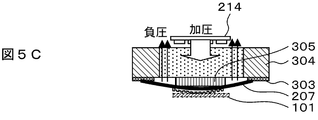
- the upper surface stamper 207 can be deformed by a small amount, and the contact surface can be enlarged from the central portion to the peripheral portion, and air bubbles can be prevented from entering between the disk substrate 101 and the upper surface stamper 207 as a transfer target. (FIG. 5C).
- the upper surface UV exposure unit 214 is used to irradiate the resist applied to the surface of the disk substrate 101 with UV light through the upper surface backup glass 206, the stamper backup elastic body 305, and the upper surface stamper 207, thereby exposing the resist. (S408) (FIG. 5D).
- the pressure in the space 307 on the back surface of the upper surface stamper 207 is lowered again while the lower surface stamper 210 is pressed against the lower surface pressing contact unit 208 by a pressing mechanism (not shown), and the disk substrate 101 is placed on the upper surface stamper 207.
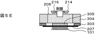
- the upper surface pressure contact unit 205 is lifted (retracted) by the drive mechanism 310 in a state in which the lower surface stamper 210 is adsorbed (S409), thereby peeling the lower surface stamper 210 from the disk substrate 101 (FIG. 5E).
- the disk substrate 101 is conveyed to the peeling unit 108 as shown in FIG.
- the disk substrate 101 is held by a disk fixture 213.
- the disk substrate 101 held by the disk fixture 213 is It completely peels from the upper surface stamper 207 (S209).
- Example 2 is almost the same as the process described in Example 1, but the process of retracting the upper surface pressure contact unit in S409 and the process of peeling the stamper from the disk substrate in S209 are different.
- the same configuration as that described in the first embodiment is used for a configuration that is not particularly described.
- the lower surface stamper 210 is not shown when the upper surface pressure contact unit 205 is retracted and the disk substrate 101 is peeled from the lower surface stamper 210 in S409.
- the pressure in the space 307 on the back surface of the upper surface stamper 207 is lowered while the pressure substrate is pressed to the lower surface pressure contact unit 208 side, the disk substrate 101 is attracted to the upper surface stamper 207, and the upper surface pressure contact unit 207 is raised.
- the space behind the lower surface stamper 210 is evacuated by the evacuation means to reduce the pressure without using the pressing mechanism.
- the disk substrate 101 is held by the disk fixture 213 of the separation unit 108 and the rear surface of the upper surface stamper 207 is removed.
- the space 307 on the back surface of the upper surface stamper 207 is evacuated by the evacuation means.
- the space 801 on the back surface of the lower stamper 210 is evacuated by a vacuum evacuation means 330 having a vacuum evacuation pump 331 and a vacuum gauge 331 connected by a vacuum pipe 332.
- a vacuum evacuation means 330 having a vacuum evacuation pump 331 and a vacuum gauge 331 connected by a vacuum pipe 332.
- the procedure for peeling the disk substrate 101 from the lower surface stamper 210 after exposing the resist corresponding to S409 is shown in FIG. 7, and the relationship between the disk substrate 101 and the upper and lower stampers 207 and 210 at that time is shown in FIGS. Shown in C.
- a procedure for peeling the disk substrate 101 from the lower surface stamper 210 first, as shown in FIG. 8A, the upper surface pressure contact unit 205 is slightly lifted by the drive mechanism 310 to the disk substrate 101 of the upper and lower stampers 207 and 210. Is released (S701), and the back surface space 308 of the lower stamper 210 is then evacuated by the exhaust means 330 (S702).
- the stamper holding portion 353 is formed of a softer material (having a higher elastic modulus) than the stamper backup elastic body 351. This deforms more greatly than the stamper backup elastic body 351. As a result, the lower surface stamper 210 is deformed more greatly in the peripheral portion in contact with the stamper holding portion 353 than in the central portion in contact with the stamper backup elastic body 351. The part is deformed into a raised shape.
- the peripheral portion is gradually peeled off from the disk substrate 101 (S703), and the space 307 on the rear surface of the upper surface stamper 207 is evacuated by an evacuation means to reduce the pressure so that the upper surface stamper 207 is removed.
- the upper surface pressing contact unit 205 is vacuum-adsorbed (S704), and the upper surface pressing contact unit 205 is lifted as shown in FIG. 101 is completely peeled from the lower surface stamper 210 (S705), and transported to the peeling unit 108 by using a transport means (not shown) (corresponding to S706: S210).
- the disk substrate 101 after exposing the resist can be peeled off from the lower surface stamper 210.
- the vacuum pump 341 and the vacuum gauge 343 connected to the peeling unit 108 by the vacuum pipe 342 are provided without using the disk fixture 213 that holds the disk substrate 101 described in the first embodiment.
- An evacuation unit 340 is provided and the back side of the disk substrate 101 is evacuated to a negative pressure to be adsorbed and held by the peeling unit 108.
- FIG. 9 shows the flow of processing in the second embodiment
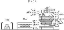
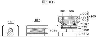
- FIG. 10 shows the relationship between the disk substrate 101, the peeling unit 108, and the upper surface stamper 207 in each processing step.
- the upper surface stamper 207 to which the disk substrate 101 peeled from the lower surface stamper 210 is closely attached is conveyed to the peeling unit 108 while being vacuum-adsorbed to the upper surface pressure contact unit 205, and is transferred to the peeling unit 108 as shown in FIG. 10A. It is mounted (S901).
- the space 309 between the disk substrate 101 and the peeling unit 108 is evacuated by the vacuum evacuation unit 340 to be in a negative pressure state, and the disk substrate 101 is adsorbed to the peeling unit 108 (S902).
- the vacuum evacuation means 320 on the upper surface pressurization and adhesion unit 205 side is operated to start exhausting the space 307 between the upper surface stamper 207 and the upper surface pressurization and adhesion unit 205 (S903), as shown in FIG. 10B.
- the upper surface stamper 207 is deformed into a convex shape and gradually peeled from the disk substrate 101 from the peripheral portion of the upper surface stamper 207 toward the center (S904), and the upper surface pressure contact unit 205 is raised by the drive mechanism 310.
- the disk substrate 101 is completely peeled from the upper surface stamper 207 (S905).
- the disk substrate 101 peeled off from the upper surface stamper 207 is stored in the disk standby area 113 after transfer by the disk discharge material handler 109 (corresponding to S906: S210).
- the back surfaces of the upper surface stamper 207 and the lower surface stamper 210 are evacuated to a negative pressure to be deformed into a convex shape, and the disk substrate 101 and the periphery from the periphery to the center portion for a very short time. Can be peeled off, and throughput can be improved.
- the upper surface stamper 207 and the lower surface stamper 210 are peeled off from the disk substrate 101 while the upper surface stamper 207 and the lower surface stamper 210 are kept in contact with the stamper holding portion 303 by evacuating the back surface, the upper surface stamper 207, the lower surface stamper 210 and the stamper are separated. Dust generation due to repeated negotiation and separation with the holding unit 303 can be prevented, and exposure can be performed in a cleaner environment.
- Example 1 and Example 2 By the method of Example 1 and Example 2 described above, it was possible to obtain a disk substrate 101 in which bubbles were prevented from entering due to fine waviness on the surface and a uniform uneven pattern was transferred to the surface.
- the stamper on which the fine pattern is formed is pressed against the magnetic disk coated with a resist on the surface. Is transferred to a resist to form a fine resist pattern on the surface of the magnetic disk.
- DESCRIPTION OF SYMBOLS 100 Microstructure transfer apparatus 101 ... Disc substrate 102 ... Disc supply material handling 103 ... Transfer part 104 ... Disc standby stage 105 ... Transfer material handling unit 106 ... Resist application unit 107 ... Transfer exposure unit 108 ... Peeling unit 109 ... Discharge material handling 110 ... Imaging unit 120 ... Control unit 130 ... Monitor 131 ... I / O device 205 ... Pressure tightness on the upper surface Adhering unit 206 ... Upper surface backup glass 207 ... Upper surface stamper 208 ... Lower surface pressure adhesion unit 209 ... Lower surface backup glass 210 ... Lower surface stamper 214 ... Upper surface UV exposure unit 2 5 ... Bottom UV exposure unit 216 ... LED 303, 353 ... Stamper holding part 304, 352 ... Pressure base 305, 351 ... Stamper backup elastic body 310 ... Drive mechanism 320, 330 340 ... Vacuum exhaust means.
Landscapes
- Engineering & Computer Science (AREA)
- Chemical & Material Sciences (AREA)
- Nanotechnology (AREA)
- Physics & Mathematics (AREA)
- Crystallography & Structural Chemistry (AREA)
- General Physics & Mathematics (AREA)
- Mathematical Physics (AREA)
- Theoretical Computer Science (AREA)
- Condensed Matter Physics & Semiconductors (AREA)
- Manufacturing & Machinery (AREA)
- Shaping Of Tube Ends By Bending Or Straightening (AREA)
- Exposure Of Semiconductors, Excluding Electron Or Ion Beam Exposure (AREA)
Abstract
微細構造転写方法およびその装置において、比較的コンパクトな装置でかつ高いスループットで泡の入り込みを防止しつつパターンの転写を実現可能にするために、微細構造を転写する方法において、表面にレジストがコーティングされた被転写体に裏面を真空吸引してスタンパを密着、加圧させる際に、スタンパを球面状に変形または湾曲させて密着面を中心部から周辺部に拡大させていくことで被転写体とスタンパとの間に気泡の入り込みを防止するようにした。
Description
本発明は、被転写体の表面にスタンパに形成された微細構造を転写する方法およびその装置に係る。
近年、半導体集積回路は微細化,集積化が進んでおり、その微細加工を実現するためのパターン転写技術としてフォトリソグラフィ装置の高精度化が進められてきた。しかし、加工方法が光露光の光源の波長に近づき、リソグラフィ技術も限界に近づいてきた。そのため、さらなる微細化,高精度化を進めるために、リソグラフィ技術に代わり、荷電粒子線装置の一種である電子線描画装置が用いられるようになった。
電子線を用いたパターン形成は、i線、エキシマレーザー等の光源を用いたパターン形成における一括露光方法とは異なり、マスクパターンを描画していく方法をとるため、描画するパターンが多ければ多いほど露光(描画)時間がかかり、パターン形成に時間がかかることが欠点とされている。そのため、256メガ、1ギガ、4ギガと、集積度が飛躍的に高まるにつれ、その分パターン形成時間も飛躍的に長くなることになり、スループットが著しく劣ることが懸念される。そこで、電子ビーム描画装置の高速化のために、各種形状のマスクを組み合わせそれらに一括して電子ビームを照射して複雑な形状の電子ビームを形成する一括図形照射法の開発が進められている。この結果、パターンの微細化が進められる一方で、電子線描画装置を大型化せざるを得ないほか、マスク位置をより高精度に制御する機構が必要になるなど、装置コストが高くなるという欠点があった。
これに対し、微細なパターン形成を低コストで行うためのインプリント技術がある。これは、基板上に形成したいパターンと同じパターンの凹凸を有するスタンパを、被転写基板表面に形成されたレジスト膜層に対して型押し、スタンパを剥離することで所定のパターンをレジスト上に転写する技術であり、シリコンウエハをスタンパとして用い、25ナノメートル以下の微細構造を転写により形成可能であるとしている。そして、インプリント技術は大容量記録媒体の記録ビット形成、半導体集積回路パターン形成等への応用が検討されてきている。
インプリント技術で、大容量記録媒体基板や半導体集積回路基板上に微細パターンを高精度に転写するには、表面に微小なうねりが発生している被転写基板表面上のパターン転写領域に均一に圧力が加わるよう、スタンパを押し付ける必要がある。
特許文献1には、光ディスクの製造方法において原版にたわみを発生させながら転写を行うことにより、表面の微細なうねりによる気泡の入り込みを防止することに関する発明が記載されている。
特許文献2および3には、スタンパを流体で加圧して湾曲させながら転写することにより表面の微細なうねりによる気泡の入り込みを防止することに関する発明が記載されている。
特許文献4には、ナノインプリントにより微細なパターンを転写する技術において、真空中または液化ガス中で転写することにより表面の微細なうねりによる気泡の入り込みを防止し、均一なパターン転写を行うことに関する発明が記載されている。
しかしながら、前記した特許文献1に記載されている転写方式は、機械固定であり、スタンパとの摺動部における発塵の影響が考慮されていない。また、微小量を連続的に変形させることが困難であることによるレジストの濡れ広がりムラが発生する点について、配慮されていない。
一方、特許文献2および3に記載されている転写方式では、スタンパ面を流体を用いて球面状にすることにより、表面の微細なうねりによる気泡の発生は抑えられるものの、流体の漏れにより発生する発塵により環境の清浄度を低下させてしまうこと、及び構造が複雑になるなどの問題があった。
さらに、特許文献4に記載された方法では、雰囲気を真空とすることにより、表面の微細なうねりによる気泡の入り込みを防止することができるが、全体を真空槽の中に入れなければならず装置が大型化してしまうとともに、真空槽への出し入れに時間がかかり、全体のスループットが低下してしまうという問題があった。
本発明の目的は、上記した従来技術の課題を解決して、比較的コンパクトな装置でかつ高いスループットで泡の入り込みを防止しつつパターンの転写を実現可能な微細構造転写方法およびその装置を提供することにある。
上記目的を達成するために、本発明では、微細構造を転写する方法において、表面にレジストがコーティングされた被転写体に裏面を真空吸引してスタンパを密着、加圧させる際に、スタンパを球面状に変形または湾曲させて密着面を中心部から周辺部に拡大させていくことで被転写体とスタンパとの間に気泡の入り込みを防止した。
すなわち、上記目的を達成するために本発明では、両面にレジストを塗布した基板の両面にパターンが形成された1対のスタンパを押し当てて1対のスタンパに形成されたパターンを基板の両面に塗布したレジストに転写する方法において、1対のスタンパをそれぞれ凸形状に変形させ、この凸形状に変形させた1対のスタンパを両面にレジストが塗布された基板の両面に垂直な方向に移動させて1対のスタンパの凸形状の中央部から周辺部に向かって徐々に基板の両面に押付け、1対のスタンパを所定の量押付けた状態で1対のスタンパの凸形状の変形を解除して1対のスタンパを基板の両面に押付け、1対のスタンパの凸形状の変形を解除して基板の両面に押付けた状態で基板の両面に塗布されたレジストにUV光を照射して基板の両面のレジストを露光し、露光したレジストが硬化した後に1対のスタンパを順次基板から剥離するようにした。
また、上記目的を達成するために本発明では、基板の両面にレジストを塗布し、この両面にレジストを塗布した基板の両面に微細なパターンが形成された1対のスタンパを押し付けて露光することにより1対のスタンパのパターンを基板の両面に塗布されたレジストに転写し、このパターンが転写されたレジストが硬化した後に基板の両面に押し付けた1対のスタンパを順次基板から剥離することにより微細構造を転写する方法において、1対のスタンパのパターンを基板の両面に塗布されたレジストに転写する工程において、1対のスタンパを凸状に変形させた状態で基板に押付け、1対のスタンパを基板に押付けた状態でスタンパの凸状の変形を解除し、この凸状の変形を解除した1対のスタンパを基板の両面に押付けた状態でUV光を照射して基板の両面に塗布されたレジストを露光することにより1対のスタンパに形成されたパターンを基板の両面に塗布されたレジストに転写するようにした。
更に、上記目的を達成するために本発明では、基板の両面にレジストを塗布するレジスト塗布ユニットと、このレジスト塗布手段により両面にレジストが塗布された基板の両面に微細なパターンが形成された1対のスタンパを押し付けて両面を露光することにより1対のスタンパのパターンを基板の両面に塗布されたレジストに転写する転写露光ユニットと、両面にパターンが転写された基板の両面に押し付けられた1対のスタンパのうち一方のスタンパから基板を剥離してこの基板を1対のスタンパのうちの他方のスタンパと一緒に転写露光ユニットから搬出する基板搬出ユニットと、この基板搬出ユニットで転写露光ユニットから搬出された基板を受けてこの基板を他方のスタンパから剥離する剥離ユニットとを備えた微細構造を転写する装置において、転写露光ユニットは、1対のスタンパをそれぞれ凸状に変形させてこの凸状の変形を解除する1対のスタンパ変形手段と、1対のスタンパをそれぞれ両面にレジストが塗布された基板の両面に対して垂直な方向に前進又は後退させる1対のスタンパ駆動手段と、1対のスタンパ駆動手段により1対のスタンパを両面にレジストが塗布された基板に押付けた状態で両面にUV光を照射して両面のレジストを露光する露光手段とを備えて構成した。
本発明によれば、比較的コンパクトな装置でかつ高いスループットで表面の微細なうねりによる気泡の入り込みを防止しつつパターンの転写を実現可能な微細構造転写方法およびその装置を実現した。
本発明に係る微細構造転写装置を実施するための形態を図を用いて説明する。
図1に本発明の第1の実施例における微細構造転写装置100の構成を示す。装置は主に、被転写物であるディスク基板101の移動を行うディスク供給マテハン102、ディスク基板101の表面に凹凸パターンを転写する転写部103、転写終了後にディスク基板101の移動を行うディスク排出用マテハン109、全体の制御を行う制御部120、入力装置130、モニタ131を備えて構成されている。
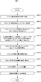
この微細構造転写装置100によりディスク基板101の両面に微細なパターンを形成する処理の流れを、図2を用いて説明する。
まず、転写前のディスク基板101は、表面に凹凸パターンを転写するためにディスク供給マテハン102により転写前ディスク待機場111から転写部103におけるディスク待機ステージ104に移動される(S201)。転写部103はディスク待機ステージ104、転写用マテハンユニット105、レジスト塗布ユニット106、転写露光ユニット107、剥離ユニット108及びレジスト塗布ユニット106から転写露光ユニット107へ搬送される途中のディスク基板101を撮像する撮像ユニット110を備えて構成され、装置の設定生産能力により、単独または複数配置される。
ディスク待機ステージ104に移送されたディスク基板101は転写用マテハンユニット105によりレジスト塗布ユニット106に移動し(S202)、ディスク基板101の両面にレジストの塗布が行われる(S203)。この塗布方式にはスピンコートまたはインクジェットなどが用いられる。塗布終了後ディスク基板101はスタンパおよび露光装置を実装された転写露光ユニット107に移動される(S204)。
移動の際、ディスク基板101は撮像ユニット110により撮像され(S205)、その画像が制御部120で処理されてディスク基板101の位置情報が取得され、転写露光ユニット107のスタンパ207および210(図3A参照)がディスク基板101の所望の位置と接触するようにディスク基板101を加圧露光ユニット107へ設置する位置座標を決定する(S206)。
スタンパ207および210の表面には微細パターンが形成されており、両面にレジスト塗布されたディスク基板101と所望の位置にて密着させ、この状態でスタンパ207及び210を介して露光光をレジストに照射して露光を行う(S207)。この露光により前述のレジストが固化し、スタンパ207及び210の表面の微細パターンがディスク基板101の両面のレジストに転写される。
次に、ディスク基板101を上側のスタンパ207に密着させた状態で下側のスタンパ210と分離し、上側のスタンパ207に密着させた状態で転写用マテハンユニット105により上側のスタンパ207とディスク基板101とを剥離ユニット108に移送される(S208)。剥離ユニット108では上側のスタンパ207とディスク基板101とを分離する(S209)。上側のスタンパ207から分離された表面のレジスト層に微細構造体が形成されたディスク基板101を、転写部103から排出用マテハン109により排出し、転写完了ディスク待機場113に格納する(S210)。また、転写露光ユニット107に装着されているスタンパ207及び210は、スタンパ待機ステージ112に格納されているスタンパと、排出用マテハン109により、適宜交換される。
制御部120は、供給マテハン102及び搬出用マテハン109によるディスク基板101のユニット間移動を行う供給マテハン102及び搬出用マテハン109を制御するマテハン制御ユニット121と、ディスク基板101の両面に塗布されるレジストを供給する図示していないレジスト供給ユニットのバルブ、モータ等を制御する制御手段を有し、レジスト膜厚、成分比の制御を行う塗布制御ユニット122と、撮像ユニット110で撮像した転写用マテハンユニット105により搬送される途中のディスク基板101の画像を解析する画像処理手段を有してディスク基板101の位置およびスタンパ207及び210のパターンの位置を算出するアライメント制御ユニット123と、スタンパ207および210の処理枚数のカウントまたは、スタンパの交換を制御するスタンパ制御ユニット124と、ディスク基板101とスタンパ207及び210のとの密着状態を検出する信号処理手段を有して転写露光ユニット107の加圧力を制御する加圧制御ユニット125と、露光時間や露光出力を制御する露光制御ユニット126と、スタンパからディスク基板を、または転写ユニットからの移動を制御する剥離制御ユニット127とを備えている。
制御部120には、入力手段130とモニタ131とが接続されている。入力手段130は、ディスク転写枚数などの製造条件や製造に必要な項目などを入力するものである。モニタ131は、装置の状態や条件などの表示、同一のスタンパで処理した累積処理枚数の表示、入力時の支援画面の表示が可能である。
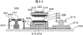
次に、表面に微細パターンが形成されたスタンパ207及び210をレジストが塗布されたディスク基板101に密着させることによりスタンパ207及び210の表面の微細パターンをディスク基板101上のレジストに転写する転写部103の処理のより詳細な動作を図3を用いて説明する。
図1でも説明したように、転写部103は主にレジスト塗布ユニット106、転写露光ユニット107、剥離ユニット108を備えて構成され、共通のベース板220上に設置されている。
まず、ディスク基板101は制御部120のステージ制御ユニット121で制御される転写用マテハンユニット105によりディスク待機ステージ104からレジスト塗布ユニット106における回転塗布用のスピンドル203上に設置される。スピンドル203は、レジストが飛散するのを防止するために防護壁201で周囲を囲われている。その後、制御部120の塗布制御ユニット122で制御してスピンドル203を回転させつつ、図示していないディスペンサからレジスト204をディスク基板101の両面に塗布し、ディスク基板101の両面にレジストの薄膜を形成させる(図3A)。
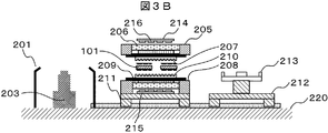
レジストの薄膜が形成されたディスク基板101を転写用マテハンユニット105により転写露光ユニット107に移動する。転写露光ユニット107は上面加圧密着ユニット205、上面バックアップガラス206、上面UV露光ユニット214、上面加圧密着ユニット205に取り付けられた上面スタンパ207、下面加圧密着ユニット208、下面バックアップガラス209、下面UV露光ユニット215、下面加圧密着ユニット208に取り付けられた下面スタンパ210を備えて構成され基台211の上に設置されている。レジストの薄膜が形成されたディスク基板101は上面スタンパ207と下面スタンパ210の間に導入される(図3B)。
その後、上面加圧密着ユニット205が駆動手段(図5参照)で駆動されて下降し、上面スタンパ207と下面スタンパ210に挟まれたディスク基板101は上面スタンパ207及び下面スタンパ210と密着する。上面スタンパ207及び下面スタンパ210の表面には微細パターンが形成されている。両面にレジストが塗布されたディスク基板101と密着した状態で上面UV露光ユニット214と下面UV露光ユニット215とから発射したUV光(Ultra Violet Light:紫外光)を上面スタンパ207及び下面スタンパ210を透過させてレジストに照射することによりレジストを露光する。この露光により前述のレジストが固化し、スタンパ表面の微細パターンがディスク基板の両面に転写される。このUV光は複数のLED(Light Emitting Diode:発光ダイオード)216を光源として発射される(図3C)。
上面スタンパ207及び下面スタンパ210に形成されている微細パターンが転写されたディスク基板101は、転写用マテハンユニット105により剥離ユニット108に移動する際に、後述するように下面スタンパ210から剥離され、上面スタンパ207側に密着された状態となる。剥離ユニット108への移動完了後、基台212上に設置されたディスク固定具213を用い、転写されたディスク基板101を固定する。その後、駆動手段で上面加圧密着ユニット205を上昇させることにより、上面スタンパ207と微細パターンが転写されたディスク基板101を分離する(図3D)。
上面スタンパ207から分離されたディスク基板101は、転写用マテハンユニット105により剥離ユニット108から取り出され、転写完了ディスク待機場113に格納される。
次に、図2におけるS207のステップ、すなわち、ディスク基板101の両面にスタンパのパターンを転写露光する工程、即ち、図3Cの工程について、図4のフロー図及び図5、図6を用いて詳細に説明する。ちなみに上面加圧密着ユニット205と下面加圧密着ユニット208は基本的には同一の機構であるので、上面加圧密着ユニット205を用いて説明する。
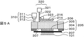
上面加圧密着ユニット205は上面スタンパ207、弾性体で形成されたスタンパ保持部303、加圧ベース304、スタンパバックアップ弾性体305、上面バックアップガラス206、上面UV露光ユニット214を備えている。ここで、スタンパ保持部303の上面スタンパ207の側の面と、スタンパバックアップ弾性体305の上面スタンパ207の側の面とは高さが同じか又はスタンパバックアップ弾性体305のほうが少し低い状態になっている。また、スタンパ保持部303は、スタンパバックアップ弾性体305よりも柔らかい(弾性率が高い)材料で形成されている。
まず、撮像ユニット110で撮像して得たディスク基板101の画像を制御部120のアライメント制御ユニット123で処理し、その結果得られたディスク基板101の位置情報に基づいて制御部120で転写用マテハンユニット105を制御して、レジストが塗布されたディスク基板101と上面スタンパ207との位置関係が所定の状態になるようにディスク基板101を露光転写ユニット107に配置する(S401)。
次に、上面スタンパ207の背面(微細パターンが形成されていない側の面)の空間を真空配管322で接続された真空排気ポンプ321と真空計323とを備えて構成される真空排気手段320により真空排気して微負圧(-5~-15kPaG程度)にすることにより、大気圧との差圧力で上面スタンパ207が吸い寄せられて上面スタンパ207の外周部付近が弾性体で形成されたスタンパ保持部303に押し付けて保持する(S402)(図5A)。
次に、真空計323で圧力を監視しながら真空排気手段320により真空排気して上面スタンパ207の背面の空間307の圧力を更に低下させる。ここでスタンパ保持部303は弾性体で形成されているため、上面スタンパ207の背面の空間307の圧力が低下するとそれによって生じる大気圧との差圧力に応じてスタンパ保持部303は上面スタンパ207の周辺部により押されて圧縮され変形する。
一方、上面スタンパ207の中心部付近はスタンパバックアップ弾性体305と接触し、大気圧との差圧力に応じてスタンパバックアップ弾性体305が上面スタンパ207の中心部付近により押し付けられて圧縮し変形する。このとき、スタンパ保持部303は、スタンパバックアップ弾性体305よりも柔らかい(弾性率が高い)材料で形成、または、真空を保持しつつ機械的に移動するため、ディスク基板101の周辺部と接触しているスタンパ保持部303の方が変形量が大きくなり、上面スタンパ207はディスク基板101の側に凸状に変形する(S403)。この上面スタンパ207の背面の空間307の圧力は-10kPa~-90kPa程度で、パターン面積およびスタンパ材質により最適値を決定する。本実施例では-20kPa~-60kPaにて変形させた(図5B)。 ここで、図6に上面スタンパ207の表面高さをプロットしたグラフ400を示す。変形前を401に、変形後を402に示す。上記にて説明した初期状態のスタンパ207はグラフの401の状態である。また、上面スタンパ207の背面の空間307が真空排気されて上面スタンパ207の外周部付近がスタンパ保持部303に押し当てられ、中心部付近がスタンパバックアップ弾性体305に押し当てられて凸形状に変形した上面スタンパ207は402の状態である。
次に、駆動軸312を介して接続されたモータ311とモータ311の出力を監視するトルクセンサ313とを備えて構成される駆動機構310により上面加圧密着ユニット205を駆動して加圧ベース304をディスク基板101方向へ移動させることにより、凸状態のスタンパ207をディスク基板101に密着させる(S404)。上面スタンパ207は凸状態のため、ディスク101の中心部から外周部に向かって順次接触していく。接触後、加圧ベース304をディスク101方向へ更に移動させることにより、加圧ベース304はさらに加圧し、凸状態のスタンパ207とディスク基板101との密着面積を増加させる。トルクセンサ313で検出されるモータ311の出力が所定の出力になり上面スタンパ207のディスク基板101への押付け力が設定加圧力に達した後、モータ311の出力を停止して駆動機構310による加圧ベース304のディスク101方向への移動を停止する(S405)。
次に、真空排気手段320による上面スタンパ207の背面の空間の真空排気を中断し(S406)、上面スタンパ207の背面の空間圧力を上昇させ、凸状に変形させた上面スタンパ207の変形を解除する。その結果、上面スタンパ207は元の平坦な状態に戻り、ディスク基板101の全面に完全に密着する(S407)。この際、上面スタンパ207の背面の空間307の圧力を -20kPa~100kPaに設定し、より確実に密着させる。上面スタンパ207の背面の空間307の圧力値は上面スタンパ207の形状および材質、パターン面積により変化する。本実施例では-20kPa~0kPaにて密着させた。これにより上面スタンパ207を微少量変形させ、密着面を中心部から周辺部に拡大させていくことが可能となり、被転写体であるディスク基板101と上面スタンパ207との間に気泡の入り込みを防止することができる(図5C)。
密着後、上面UV露光ユニット214を用い、上面バックアップガラス206、スタンパバックアップ弾性体305および上面スタンパ207を通して、ディスク基板101表面に塗布されたレジストにUV光を照射して露光し、レジストを硬化させる(S408)(図5D)。
レジスト硬化後、下面スタンパ210を図示していない押さえ機構で下面加圧密着ユニット208の側に押さえ込んだ状態で再度上面スタンパ207の背面の空間307の圧力を低下させ、上面スタンパ207にディスク基板101を吸着させた状態で駆動機構310により上面加圧密着ユニット205を上昇(後退)させる(S409)ことにより、ディスク基板101から下面スタンパ210を剥離する(図5E)。
その後、図2で説明したように、ディスク基板101を上面スタンパ207に吸着した状態で図示していないハンドリングユニットで図3Dに示すように剥離ユニット108へ搬送される。剥離ユニット108において、ディスク基板101はディスク固定具213により保持される。この状態で上面スタンパ207の背面の空間307の圧力を大気圧に戻し、駆動機構310により上面加圧密着ユニット205を保持して上昇させると、ディスク固定具213に保持されているディスク基板101は上面スタンパ207から完全に剥離する(S209)。
実施例2は実施例1で説明した工程とほとんど同じ工程であるが、S409における上面加圧密着ユニットを後退させる工程、及び、S209におけるスタンパをディスク基板から剥離する工程が異なる。また、実施例2では、特に説明していない構成については、実施例1で説明したものと同じ構成を用いる。
即ち、上記実施例1においては、S408でレジストを露光した後、S409において上面加圧密着ユニット205を後退させてディスク基板101を下面スタンパ210から剥離するときに、下面スタンパ210を図示していない押さえ機構で下面加圧密着ユニット208の側に押さえ込んだ状態で上面スタンパ207の背面の空間307の圧力を低下させて上面スタンパ207にディスク基板101を吸着させ、上面加圧密着ユニット207を上昇させることによりディスク基板101を下面スタンパ210から剥離させる方法を説明したが、実施例2においては、押さえ機構を用いずに、下面スタンパ210の背面の空間を排気手段で真空排気して圧力を低下させ、下面スタンパ210を凸状に変形させることにより、下面スタンパ210に密着しているディスク基板101を外周部から徐々に剥離させる方式を採用した。
また、S209で剥離ユニット108においてディスク基板101を上面スタンパ207から剥離する方法として、実施例1においては、ディスク基板101を剥離ユニット108のディスク固定具213で保持した状態で上面スタンパ207の背面の空間307の圧力を大気圧に戻して、上面加圧密着ユニット205を上昇させることにより剥離する方法について説明したが、実施例2においては、上面スタンパ207の背面の空間307を排気手段で真空排気して圧力を低下させ、上面スタンパ207を凸状に変形させることにより、上面スタンパ207に密着しているディスク基板101を外周部から徐々に剥離させる方式を採用した。
先ず、実施例2におけるレジストを露光した後にS409に相当するステップにおいて、ディスク基板101を下面スタンパ210から剥離する方式について説明する。本実施例においては、図8Aに示すように、下面スタンパ210の背面の空間801を真空配管332で接続された真空排気ポンプ331と真空計331とを備えた真空排気手段330で真空排気して圧力を低下させて下面スタンパ210を凸状に変形させることにより、下面スタンパ210に密着しているディスク基板101を外周部から徐々に剥離させる。本実施例を、図を用いて説明する。
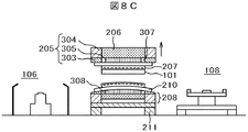
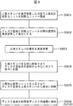
本実施例において、S409に相当するレジストを露光した後にディスク基板101を下面スタンパ210から剥離する手順を図7に、そのときのディスク基板101と上下のスタンパ207と210との関係を図8A~Cに示す。ディスク基板101を下面スタンパ210から剥離する手順としては、先ず、図8Aに示すように、駆動機構310により上面加圧密着ユニット205を少し上昇させて上下のスタンパ207と210とのディスク基板101への全面押し付けを解除し(S701)、次に下面スタンパ210の裏面空間308を排気手段330で真空排気する(S702)。
下面スタンパ210の裏面空間308を真空排気すると、大気圧との差により下面スタンパ210は下面加圧密着ユニット208のスタンパバックアップ弾性体351と加圧ベース352上のスタンパ保持部353とに押し付けられる。上面加圧密着ユニット205と同様に、下面加圧密着ユニット208においても、スタンパ保持部353はスタンパバックアップ弾性体351よりも柔らかい(弾性率が高い)材料で形成されているため、スタンパ保持部353の方がスタンパバックアップ弾性体351よりも大きく変形する。その結果、下面スタンパ210はスタンパ保持部353と接している周辺部のほうがスタンパバックアップ弾性体351と接している中央部と比べて大きく変形するため、下面スタンパ210は、図8Bに示すように中央部が盛り上がっている凸形状に変形する。
下面スタンパ210をこのように変形させることにより周辺部分から徐々にディスク基板101から剥離させ(S703),上面スタンパ207の背面の空間307を排気手段で真空排気し圧力を低下させて上面スタンパ207を上面加圧密着ユニット205に真空吸着させ(S704),図8Cに示すように上面加圧密着ユニット205を上昇させることで真空吸着された上面スタンパ207とこの上面スタンパ207に密着しているディスク基板101とを下面スタンパ210から完全に剥離し(S705)、図示していない搬送手段を用いて剥離ユニット108へ搬送する(S706:S210に相当)。
これにより、レジストを露光した後のディスク基板101を、下面スタンパ210から剥離させることができる。
なお、図8A乃至Cにおいては、図3A乃至Dで説明したLED216を用いた上面UV露光ユニット214と下面UV露光ユニット215の記載を省略しているが、図8A乃至Cに記載した本実施例においても実施例1の場合と同様にLED216を用いた上面UV露光ユニット214と下面UV露光ユニット215を備えている。
次に、剥離ユニット108において、実施例2における上面スタンパ207に密着しているディスク基板101を上面スタンパ207から剥離させる方式について説明する。
本実施例においては、実施例1で説明したディスク基板101を保持するディスク固定具213を用いずに、剥離ユニット108に真空配管342で接続された真空排気ポンプ341と真空計343とを備えた真空排気手段340を設けてディスク基板101の裏面側を真空排気して負圧にすることにより剥離ユニット108に吸着させて保持する構成とした。実施例2における処理の流れを図9に、また各処理工程におけるディスク基板101と剥離ユニット108及び上面スタンパ207との関係を図10に示す。
まず、下面スタンパ210から剥離されたディスク基板101を密着させた上面スタンパ207は上面加圧密着ユニット205に真空吸着された状態で剥離ユニット108に搬送され、図10Aに示すように剥離ユニット108に載置される(S901)。次に、真空排気手段340によりディスク基板101と剥離ユニット108との間の空間309を排気して負圧の状態にしてディスク基板101を剥離ユニット108に吸着させる(S902)。この状態で、上面加圧密着ユニット205の側の真空排気手段320を作動させて上面スタンパ207と上面加圧密着ユニット205との間の空間307の排気を開始し(S903),図10Bに示すように上面スタンパ207を凸形状に変形させて上面スタンパ207の周辺部分から中心に向けて徐々にディスク基板101から剥離させ(S904),駆動機構310により上面加圧密着ユニット205を上昇させることにより、図10Cに示すようにディスク基板101を上面スタンパ207から完全に剥離させる(S905)。上面スタンパ207から剥離されたディスク基板101は、ディスク排出用マテハン109により転写後ディスク待機場113に格納される(S906:S210に相当)。
本実施例によれば、上面スタンパ207及び下面スタンパ210の裏面を真空に排気して負圧の状態にすることにより凸状に変形させてディスク基板101と周辺から中央部に向かって極短時間で剥離させることが可能になり、スループットを向上させることが可能になる。
また、裏面を真空に排気することにより上面スタンパ207及び下面スタンパ210がそれぞれスタンパ保持部303と接触を維持した状態でディスク基板101との剥離が行われるので、上面スタンパ207及び下面スタンパ210とスタンパ保持部303との折衝区と分離を繰返すことによる発塵を防ぐことができ、よりクリーンな環境で露光を行うことが可能になる。
以上に説明した実施例1及び実施例2の方法により、表面の微細なうねりによる気泡入り込みを防止し、表面に均一な凹凸パターンが転写されているディスク基板101を得ることができた。
上記に説明したスタンパに形成された微細なパターンのディスク基板101への転写をディスク基板101の両面に同時に行うことにより、ディスク基板101の両面に均一な凹凸パターンを転写することができる。
本発明は、磁気ディスクの表面に磁気記録用の微細なパターンを形成するためのレジストパターン形成工程において、微細なパターンが形成されているスタンパを表面にレジストが塗布された磁気ディスクに押し付けてスタンパのパターンをレジストに転写することにより磁気ディスクの表面にレジストの微細なパターンを形成することに使用される。
100・・・微細構造転写装置 101・・・ディスク基板 102・・・ディスク供給マテハン 103・・・転写部 104・・・ディスク待機ステージ 105・・・転写用マテハンユニット 106・・・レジスト塗布ユニット 107・・・転写露光ユニット 108・・・剥離ユニット 109・・・排出用マテハン 110・・・撮像ユニット 120・・・制御ユニット 130・・・モニタ 131・・・入出力装置 205・・・上面加圧密着ユニット 206・・・上面バックアップガラス 207・・・上面スタンパ 208・・・下面加圧密着ユニット 209・・・下面バックアップガラス 210・・・下面スタンパ 214・・・上面UV露光ユニット 215・・・下面UV露光ユニット 216・・・LED 303,353・・・スタンパ保持部 304,352・・・加圧ベース 305,351・・・スタンパバックアップ弾性体 310・・・駆動機構 320,330,340・・・真空排気手段。
Claims (16)
- 両面にレジストを塗布した基板の前記両面にパターンが形成された1対のスタンパを押し当てて該1対のスタンパに形成されたパターンを前記基板の前記両面に塗布したレジストに転写する方法であって、
前記1対のスタンパをそれぞれ凸形状に変形させ、
該凸形状に変形させた1対のスタンパを前記両面にレジストが塗布された基板の前記両面に垂直な方向に移動させて前記1対のスタンパの凸形状の中央部から周辺部に向かって徐々に前記基板の両面に押付け、
前記1対のスタンパを所定の量押付けた状態で前記1対のスタンパの凸形状の変形を解除して前記1対のスタンパを前記基板の両面に押付け、
前記1対のスタンパの凸形状の変形を解除して前記基板の両面に押付けた状態で前記基板の両面に塗布されたレジストにUV光を照射して前記基板の両面のレジストを露光し、 前記露光したレジストが硬化した後に前記1対のスタンパを順次前記基板から剥離することを特徴とする微細構造転写方法。 - 前記1対のスタンパを順次前記基板から剥離することを、前記1対のスタンパの一方を凸状に変形させて前記基板の周辺部から前記一方のスタンパを剥離させ、次に前記1対のスタンパのうちの他方のスタンパを凸状に変形させて前記基板の周辺部から前記他方のスタンパを剥離させることを特徴とする請求項1に記載の微細構造転写方法。
- 前記1対のスタンパを順次前記基板から剥離するときに前記1対のスタンパをそれぞれ凸状に変形させることを、前記1対のスタンパのそれぞれと前記基板に対して反対側の面の側の空間を真空に排気することにより行うことを特徴とする請求項2に記載の微細構造転写方法。
- 基板の両面にレジストを塗布し、
該両面にレジストを塗布した基板の該両面に微細なパターンが形成された1対のスタンパを押し付けて露光することにより該1対のスタンパのパターンを前記基板の両面に塗布されたレジストに転写し、
該パターンが転写されたレジストが硬化した後に前記基板の両面に押し付けた1対のスタンパを順次前記基板から剥離する
ことにより微細構造を転写する方法であって、
前記1対のスタンパのパターンを前記基板の両面に塗布されたレジストに転写する工程において、
前記1対のスタンパを凸状に変形させた状態で前記基板に押付け、
前記1対のスタンパを前記基板に押付けた状態で前記スタンパの凸状の変形を解除し、 該凸状の変形を解除した1対のスタンパを前記基板の両面に押付けた状態でUV光を照射して前記基板の両面に塗布されたレジストを露光する
ことにより前記1対のスタンパに形成されたパターンを前記基板の両面に塗布されたレジストに転写することを特徴とする微細構造転写方法。 - 前記1対のスタンパのそれぞれ前記基板と向き合う面の反対側の面の側を真空に排気することにより前記1対のスタンパをそれぞれ凸形状に変形させることを特徴とする請求項1又は4に記載の微細構造転写方法。
- 前記1対のスタンパのそれぞれ前記基板と向き合う面の反対側の面の側を中央部と周辺部とで弾性率が異なる材料で支持して真空に排気することにより前記1対のスタンパをそれぞれ凸形状に変形させることを特徴とする請求項1又は4に記載の微細構造転写方法。
- 前記弾性率が異なる材料は、前記中心部よりも前記周辺部を支持する材料のほうが弾性率が大きいことを特徴とする請求項4に記載の微細構造転写方法。
- 基板の両面にレジストを塗布するレジスト塗布ユニットと、
該レジスト塗布手段により両面にレジストが塗布された基板の両面に微細なパターンが形成された1対のスタンパを押し付けて前記両面を露光することにより該1対のスタンパのパターンを前記基板の両面に塗布されたレジストに転写する転写露光ユニットと、
前記両面にパターンが転写された基板の前記両面に押し付けられた1対のスタンパのうち一方のスタンパから前記基板を剥離して該基板を前記1対のスタンパのうちの他方のスタンパと一緒に前記転写露光ユニットから搬出する基板搬出ユニットと、
該基板搬出ユニットで前記転写露光ユニットから搬出された基板を受けて該基板を前記他方のスタンパから剥離する剥離ユニットと
を備えた微細構造を転写する装置であって、前記転写露光ユニットは、
前記1対のスタンパをそれぞれ凸状に変形させて該凸状の変形を解除する1対のスタンパ変形手段と、
前記1対のスタンパをそれぞれ前記両面にレジストが塗布された基板の前記両面に対して垂直な方向に前進又は後退させる1対のスタンパ駆動手段と、
前記1対のスタンパ駆動手段により前記1対のスタンパを前記両面にレジストが塗布された基板に押付けた状態で前記両面にLEDを用いたUV光を照射して前記両面のレジストを露光する露光手段と
を有することを特徴とする微細構造転写装置。 - 前記1対のスタンパ変形手段はそれぞれ前記1対のスタンパの何れか一方と対応し、該何れか一方のスタンパに対応するスタンパ変形手段は、前記一方のスタンパの前記基板と向き合う面の反対側の面の側を真空に排気する真空排気部と、該真空排気部で真空に排気された状態で前記一方のスタンパの前記基板と向き合う面の反対側の面の外周部付近を支持する第1の弾性部材と、前記真空排気部で真空に排気された状態で前記一方のスタンパの前記基板と向き合う面の反対側の面の中央部付近を支持する第2の弾性部材とを有することを特徴とする請求項8記載の微細構造転写装置。
- 前記第1の弾性部材は、前記第2の弾性部材よりも弾性率が大きいことを特徴とする請求項9記載の微細構造転写装置。
- 前記1対のスタンパ駆動手段は、前記1対のスタンパ変形手段で凸状に変形させた前記1対のスタンパを前記両面にレジストが塗布された基板の両面に対して垂直な方向に前進させて前記凸状に変形させた1対のスタンパを前記両面にレジストが塗布された基板の該両面に押付けることを特徴とする請求項8記載の微細構造転写装置。
- 前記1対のスタンパ変形手段はそれぞれ、前記1対のスタンパ駆動手段のうちの一方のスタンパ駆動手段で前記凸状に変形させたスタンパを前記両面にレジストが塗布された基板の一方の面に一定量押付けた状態で前記スタンパの凸状の変形を解除することを特徴とする請求項8記載の微細構造転写装置。
- 前記転写露光ユニットは、該1対のスタンパ変形手段による前記1対のスタンパの凸状の変形を解除して前記1対のスタンパを前記1対のスタンパ駆動手段で前記基板の両面に押付けた状態で該基板の両面にLEDを用いたUV光を照射して前記基板の両面のレジストを露光することを特徴とする請求項8記載の微細構造転写装置。
- 前記転写露光ユニットは、前記1対のスタンパ変形手段による前記1対のスタンパの凸状の変形を解除して前記1対のスタンパを前記1対のスタンパ駆動手段で前記基板の両面に押付けた状態で、前記第2の弾性部材を支持するバックアップガラスおよび前記第2の弾性部材を通し該基板の両面にLEDから発射されたUV光を照射して前記基板の両面のレジストを露光することを特徴とする請求項8記載の微細構造転写装置。
- 前記1対のスタンパ変形手段は、前記露光手段で前記両面にレジストが塗布された基板の前記両面に前記1対のスタンパを押し付けて露光して前記レジストを硬化させた後に、前記露光転写ユニットにおいて、前記1対のスタンパ変形手段のうちの一方のスタンパ変形手段により前記1対のスタンパのうちの一方のスタンパを凸状に変形させて前記基板の周辺部から前記一方のスタンパと剥離させることにより前記一方のスタンパを前記基板の一方の面から剥離し、前記剥離ユニットにおいて、前記1対のスタンパ変形手段のうちの他方のスタンパ変形手段により前記1対のスタンパのうちの他方のスタンパを凸状に変形させて前記基板の周辺部から前記他方のスタンパと剥離させることにより前記他方のスタンパを前記基板の他方の面から剥離することを特徴とする請求項8記載の微細構造転写装置。
- 前記1対のスタンパ変形手段は、それぞれ、前記真空排気部で前記スタンパの前記基板と向き合う面の反対側の面の側を真空に排気することにより前記1対のスタンパをそれぞれ凸状に変形させて前記1対のスタンパをそれぞれ前記基板の両面から剥離することを特徴とする請求項15記載の微細構造転写装置。
Applications Claiming Priority (4)
| Application Number | Priority Date | Filing Date | Title |
|---|---|---|---|
| JP2010-050631 | 2010-03-08 | ||
| JP2010050631 | 2010-03-08 | ||
| JP2010-262320 | 2010-11-25 | ||
| JP2010262320A JP5469041B2 (ja) | 2010-03-08 | 2010-11-25 | 微細構造転写方法およびその装置 |
Publications (1)
| Publication Number | Publication Date |
|---|---|
| WO2011111441A1 true WO2011111441A1 (ja) | 2011-09-15 |
Family
ID=44531588
Family Applications (1)
| Application Number | Title | Priority Date | Filing Date |
|---|---|---|---|
| PCT/JP2011/052052 Ceased WO2011111441A1 (ja) | 2010-03-08 | 2011-02-01 | 微細構造転写方法およびその装置 |
Country Status (3)
| Country | Link |
|---|---|
| US (1) | US8764431B2 (ja) |
| JP (1) | JP5469041B2 (ja) |
| WO (1) | WO2011111441A1 (ja) |
Families Citing this family (17)
| Publication number | Priority date | Publication date | Assignee | Title |
|---|---|---|---|---|
| KR101304149B1 (ko) * | 2010-09-27 | 2013-09-05 | (주)엘지하우시스 | 3차원 패턴 형성용 성형 몰드 및 이를 이용한 가전제품 외장재 제조 방법 |
| JP5782784B2 (ja) * | 2011-03-31 | 2015-09-24 | 大日本印刷株式会社 | インプリント方法およびそれを実施するためのインプリント装置 |
| JP2013118233A (ja) * | 2011-12-02 | 2013-06-13 | Hitachi High-Technologies Corp | 微細構造転写装置 |
| JP5938218B2 (ja) | 2012-01-16 | 2016-06-22 | キヤノン株式会社 | インプリント装置、物品の製造方法およびインプリント方法 |
| JP6019685B2 (ja) * | 2012-04-10 | 2016-11-02 | 大日本印刷株式会社 | ナノインプリント方法及びナノインプリント装置 |
| US10343312B2 (en) | 2012-08-27 | 2019-07-09 | Scivax Corporation | Imprint device and imprint method |
| US9177790B2 (en) * | 2013-10-30 | 2015-11-03 | Infineon Technologies Austria Ag | Inkjet printing in a peripheral region of a substrate |
| SG11201608362TA (en) * | 2014-04-22 | 2016-11-29 | Ev Group E Thallner Gmbh | Method and device for embossing of a nanostructure |
| JP6375718B2 (ja) * | 2014-06-24 | 2018-08-22 | 大日本印刷株式会社 | インプリントモールド用基材、インプリントモールド及びそれらの製造方法、並びにインプリントモールド用基材の評価方法 |
| JP6406544B2 (ja) * | 2014-10-29 | 2018-10-17 | トヨタ自動車株式会社 | 非水電解液二次電池および該電池に用いられる電極体 |
| JP5867578B2 (ja) * | 2014-12-22 | 2016-02-24 | 大日本印刷株式会社 | インプリント用モールド複合体およびその製造方法 |
| JP6553926B2 (ja) * | 2015-04-09 | 2019-07-31 | キヤノン株式会社 | インプリント装置、インプリント方法、および物品の製造方法 |
| CN108475025B (zh) | 2015-11-20 | 2021-02-26 | Asml荷兰有限公司 | 光刻设备和操作光刻设备的方法 |
| TWI672212B (zh) * | 2016-08-25 | 2019-09-21 | 國立成功大學 | 奈米壓印組合體及其壓印方法 |
| KR20250153308A (ko) * | 2019-12-02 | 2025-10-24 | 에베 그룹 에. 탈너 게엠베하 | 스탬프를 분리하는 방법 및 장치 |
| CN115812179B (zh) * | 2020-07-06 | 2026-02-27 | Ev集团E·索尔纳有限责任公司 | 制造微结构及/或奈米结构之方法及装置 |
| KR102523787B1 (ko) * | 2022-02-03 | 2023-04-21 | 주식회사피에스디이 | 기포 문제를 해결하기 위한 임프린팅 장치 및 임프린팅 방법 |
Citations (6)
| Publication number | Priority date | Publication date | Assignee | Title |
|---|---|---|---|---|
| JP2001068411A (ja) * | 1999-07-28 | 2001-03-16 | Lucent Technol Inc | デバイス製作のためのリソグラフィ・プロセス |
| JP2004288845A (ja) * | 2003-03-20 | 2004-10-14 | Hitachi Ltd | ナノプリント用スタンパ、及び微細構造転写方法 |
| JP2008524854A (ja) * | 2004-12-16 | 2008-07-10 | エーエスエムエル ホールディング エヌ.ブイ. | インプリントリソグラフィに使用されるナノディスクを形成するためのシステムおよび方法ならびにそれによって形成されたナノディスクおよびメモリディスク |
| JP2009518863A (ja) * | 2005-12-08 | 2009-05-07 | モレキュラー・インプリンツ・インコーポレーテッド | 基板の両面パターニングする方法及びシステム |
| JP2009123318A (ja) * | 2007-10-23 | 2009-06-04 | Tdk Corp | インプリント方法、情報記録媒体製造方法およびインプリントシステム |
| JP2010507230A (ja) * | 2006-10-13 | 2010-03-04 | ヒューレット−パッカード デベロップメント カンパニー エル.ピー. | コンタクトリソグラフィ装置、システム及び方法 |
Family Cites Families (12)
| Publication number | Priority date | Publication date | Assignee | Title |
|---|---|---|---|---|
| JPS5829631A (ja) * | 1981-08-18 | 1983-02-21 | Matsushita Electric Ind Co Ltd | 平板状情報記録担体の複製装置 |
| JPH02126434A (ja) * | 1988-11-05 | 1990-05-15 | Mitsubishi Electric Corp | 光デイスク基板成形方法 |
| JP2005537656A (ja) * | 2002-08-27 | 2005-12-08 | オブデュキャット、アクチボラグ | 対象物にパターンを転写するための装置 |
| JP2004303385A (ja) | 2003-04-01 | 2004-10-28 | Sony Corp | 光ディスクのピット転写工程におけるディスクとスタンパーのセット方法及び装置 |
| JP2005043652A (ja) * | 2003-07-22 | 2005-02-17 | Fuji Xerox Co Ltd | 高分子光導波路の製造方法及びその製造装置 |
| JP4441675B2 (ja) | 2004-07-05 | 2010-03-31 | 株式会社日立製作所 | 転写印刷機及び転写印刷方法 |
| US8377361B2 (en) * | 2006-11-28 | 2013-02-19 | Wei Zhang | Imprint lithography with improved substrate/mold separation |
| JP4418476B2 (ja) * | 2007-03-20 | 2010-02-17 | 株式会社日立ハイテクノロジーズ | 微細構造転写装置および微細構造体の製造方法 |
| KR101289337B1 (ko) * | 2007-08-29 | 2013-07-29 | 시게이트 테크놀로지 엘엘씨 | 양면 임프린트 리소그래피 장치 |
| JP5433223B2 (ja) | 2008-02-20 | 2014-03-05 | 東芝機械株式会社 | 転写装置および転写方法 |
| JP2010093105A (ja) * | 2008-10-09 | 2010-04-22 | Toshiba Mach Co Ltd | 被成型品保持装置、型保持装置および転写装置 |
| JP5416420B2 (ja) * | 2009-01-22 | 2014-02-12 | 株式会社日立ハイテクノロジーズ | 微細構造転写装置 |
-
2010
- 2010-11-25 JP JP2010262320A patent/JP5469041B2/ja not_active Expired - Fee Related
-
2011
- 2011-02-01 WO PCT/JP2011/052052 patent/WO2011111441A1/ja not_active Ceased
- 2011-02-11 US US13/025,694 patent/US8764431B2/en not_active Expired - Fee Related
Patent Citations (6)
| Publication number | Priority date | Publication date | Assignee | Title |
|---|---|---|---|---|
| JP2001068411A (ja) * | 1999-07-28 | 2001-03-16 | Lucent Technol Inc | デバイス製作のためのリソグラフィ・プロセス |
| JP2004288845A (ja) * | 2003-03-20 | 2004-10-14 | Hitachi Ltd | ナノプリント用スタンパ、及び微細構造転写方法 |
| JP2008524854A (ja) * | 2004-12-16 | 2008-07-10 | エーエスエムエル ホールディング エヌ.ブイ. | インプリントリソグラフィに使用されるナノディスクを形成するためのシステムおよび方法ならびにそれによって形成されたナノディスクおよびメモリディスク |
| JP2009518863A (ja) * | 2005-12-08 | 2009-05-07 | モレキュラー・インプリンツ・インコーポレーテッド | 基板の両面パターニングする方法及びシステム |
| JP2010507230A (ja) * | 2006-10-13 | 2010-03-04 | ヒューレット−パッカード デベロップメント カンパニー エル.ピー. | コンタクトリソグラフィ装置、システム及び方法 |
| JP2009123318A (ja) * | 2007-10-23 | 2009-06-04 | Tdk Corp | インプリント方法、情報記録媒体製造方法およびインプリントシステム |
Also Published As
| Publication number | Publication date |
|---|---|
| US8764431B2 (en) | 2014-07-01 |
| JP2011211157A (ja) | 2011-10-20 |
| JP5469041B2 (ja) | 2014-04-09 |
| US20110217479A1 (en) | 2011-09-08 |
Similar Documents
| Publication | Publication Date | Title |
|---|---|---|
| JP5469041B2 (ja) | 微細構造転写方法およびその装置 | |
| JP4596981B2 (ja) | インプリント装置、及び微細構造転写方法 | |
| KR101622818B1 (ko) | 나노임프린팅 방법 및 나노임프린팅 방법을 실행하기 위한 나노임프린팅 장치 | |
| JP2010067796A (ja) | インプリント装置 | |
| JP2011150780A (ja) | 両面インプリント装置 | |
| JP2008221552A (ja) | 微細構造転写装置、スタンパおよび微細構造の製造方法 | |
| US9405193B2 (en) | Imprint apparatus, imprint method and article manufacturing method | |
| JP7033994B2 (ja) | 成形装置及び物品の製造方法 | |
| WO2011111792A1 (ja) | 微細構造転写装置及び微細構造転写方法 | |
| US20210129520A1 (en) | Method and device for embossing of a nanostructure | |
| JP2019041005A (ja) | リソグラフィ装置、および物品の製造方法 | |
| JP2007194304A (ja) | インプリント装置およびインプリント方法 | |
| TW201817569A (zh) | 壓印裝置、壓印方法及物品製造方法 | |
| JP2019186347A (ja) | 加工装置、インプリント装置、平坦化装置、および加工方法 | |
| JP2014069339A (ja) | スタンパ、スタンパ製造装置及びその製造方法並びに微細構造転写方法 | |
| JP2012099789A (ja) | インプリント装置、及び、物品の製造方法 | |
| JP2010283108A (ja) | インプリント装置及び物品の製造方法 | |
| JP2018006554A (ja) | パターン形成装置、インプリント装置および物品の製造方法 | |
| JP2013022807A (ja) | 微細構造転写装置及びスタンパ移送方法 | |
| US12339584B2 (en) | Substrate conveyance method, substrate conveyance apparatus, molding method, and article manufacturing method | |
| JP2019220526A (ja) | 型を用いて基板上の組成物を成形する成形装置、成形方法、および、物品の製造方法 | |
| JP2019149532A (ja) | インプリント方法及び製造方法 | |
| JP2012099197A (ja) | 光インプリント方法 | |
| JP2024055320A (ja) | インプリント装置及び物品の製造方法 | |
| JP2024082116A (ja) | インプリント方法、インプリント装置及び物品の製造方法 |
Legal Events
| Date | Code | Title | Description |
|---|---|---|---|
| 121 | Ep: the epo has been informed by wipo that ep was designated in this application |
Ref document number: 11753103 Country of ref document: EP Kind code of ref document: A1 |
|
| NENP | Non-entry into the national phase |
Ref country code: DE |
|
| 122 | Ep: pct application non-entry in european phase |
Ref document number: 11753103 Country of ref document: EP Kind code of ref document: A1 |